1
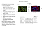
M501 Hardware Specifications
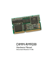
SoC: ATMEL AT91RM9200
CPU: ARM920T ARM Thumb Processor with Memory Management Unit (MMU)
Clock: 180MHz
SDRAM: 64MB
Flash: 16MB Intel StrataFlash or Equivalent
Ethernet: 10/100 Mbps with MAC/PHY and Transformer
PHY: DAVCOM DM9161
Transformer: 1.5 KV isolation
Signal: ETX0+, ETX0-, ERX0+, ERXUSB : USB 2.0 full speed (12Mbps) Host x2
Signal: UDataA+, UDataA-, UDataB+, UDataBUART: Four Universal Asynchronous Receiver and Transmitter
Data Bits: 5 to 9 bits
Parity: None, Even, Odd, Mark, Space
Stop: 1, 1.5, 2 bits
Baud Rate: Up to 921.6 Kbps
Flow Control: RTS/CTS, XON/XOFF, None
Multi-drop Mode with address generation and detection (COM1 only)
RS485 Driver Control Signal (COM1:RTS0)
Signal Level: CMOS/3.3V compatible
COM1: TXD0, RXD0, RTS0, CTS0 (RS485 Control: RTS0)
(Software configurable RS-232/422/485)
COM2: TXD1, RXD1, RTS1, CTS1, DCD1, DTR1, DSR1
( RS-232 with full modem control)
COM3: TXD2, RXD2, RTS2, CTS2
(RS-232 with hardware flow control)
COM4: TXD3, RXD3, RTS3, CTS3
(RS-232 with hardware flow control)
Inter-IC Bus: (I2C Bus)
Compatible with standard two-wire serial memory interface
Supported Devices: (Driver built-in)
Real Time Clock: Ricoh (RS5C372)
EEPROM: ATMEL AT24C16 and compatible
Signal: TWD, TWDK
I2S (internal IC Sound):
Transmitter: TSCK, TWS, TSD
Receiver: RSCK, RWS, RSD
Serial Peripheral Interface: (SPI)
Two chip Selects with external decoder
Three wires signals: MISO, MOSI and SPCK clock
Signal: MISO, MOSI, SPCK, CS1, CS2
Multimedia Card Interface
Compatible with SD memory card Specification 1.0
Signal: MCCDA, MCCK, MCDA0, MCDA1, MCDA2, MCDA3
Watchdog Timer: CPU built-in WDT and used by Linux Kernel
Programmable DIO
32 General Purpose IOs and can be programmable as digital input or output
Support interrupt function for digital inputs
Signal Level: CMOS/3.3V Compatible
Input:
Low level: -0.3V min
+0.8V max
High level: +2V min
+3.9V max
Output:
Low level: +0.4V max @0mA
+0.2V min @ 8mA
High level: +3.1V max @0mA
+2.9V min @ 8mA
Signal: PIO0 to PIO31
External Bus Interface:
8-bit data bus
Signal: D0~D7
8-bit address bus
Signal: A0~A7
4 Chip Selection
Signal: NCS3~NCS6
Signal Level: CMOS/3.3V
Predefine Pins:
Reset Button (CN2, pin#35, RST#1), input
Buzzer (CN2, pin#37, BUZR), output
System ready LED (CN2, pin#38, RDY_LED), output
LAN activity LED (CN3, pin#11, ACT_LED), output
Undefined Digital IO Pins (reserved)
CN1: pin#23, #24, #25, #26
CN3: pin#23, #24
Debug Port:
Serial Console: Tx/Rx
Signal: Tx share with RTS2
Rx share with CTS2
JTAG: For low level debug
Signal: NTRST, TDI, TMS, TCK, TDO
Power:
Input: 3.0 to 3.6VDC (3.3V nominal)
Consumption: 2.5W