1
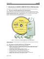
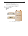
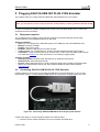
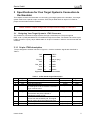
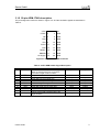
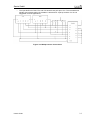
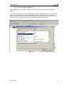
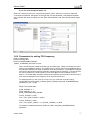
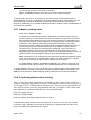
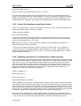
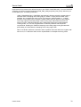
SAU510-USB ISO PLUS
JTAG Emulator
User’s Guide
Sauris GmbH
Rev. A. May 2009
IMPORTANT NOTICE
Sauris GmbH reserves the right to make changes to its products or to discontinue any product or service
without notice, and advises its customers to obtain the latest version of relevant information to verify, before
placing orders, that the information being relied on is current. Sauris GmbH warrants performance of its
products and related software to current specifications in accordance with our standard warranty. Testing
and other quality control techniques are utilized to the extent deemed necessary to support this warranty.
Please be aware that the products described herein are not intended for use in life-support appliances,
devices, or systems. Sauris GmbH assumes no liability for applications assistance, customer product
design, software performance, or infringement of patents or services described herein. Nor does
Sauris GmbH warrant or represent any license, either express or implied, is granted under any patent right,
copyright, or other intellectual property right of Sauris GmbH covering or relating to any combination,
machine, or process in which such Digital Signal Processing development products or services might be or
are used.
WARNING
This equipment is to be used in laboratory facilities only. It generates, uses, and can radiate
electromagnetic energy and has not been tested for compliance with the limits of computing devices
according to clause J, part 15, FCC rules, that are designed to specify the acceptable level of
electromagnetic interference. Operation of this equipment may cause radio interference.
TRADEMARKS
Windows 98, Windows 2000, Windows XP and Windows Vista are registered trademarks of Microsoft Corp.
Code Composer and Code Composer Studio are registered trademarks of Texas Instruments.
Copyright © 2009 Sauris GmbH.
Dear developers!
1. Sauris GmbH pleased to recommend you ask your technical questions on our forum.
You can find answers to your questions on the forum pages and add a new topic to discuss the problem
with our engineers.
2. We suggest you to read WiKi, where you can find the full description of the functionality of our products.
Please register and ask your question.
Please, don't forget to subscribe to new topics to keep track of the status of your question.
You will be informed by e-mail when our engineers respond to the message.
3. Dear Friends, you could join projects support program right now sending us RFQ, Technical
Questions or Samples Order. Also you can find warranty terms on our web.
User’s Guide
2
Sauris GmbH
Contents
1 Introduction to SAU510-USB ISO PLUS JTAG Emulator.......................................... 4
1.1
Overview of SAU510-USB ISO PLUS JTAG Emulator .................................. 4
1.2
Key Features of SAU510-USB PLUS JTAG Emulator .................................... 4
1.3
Key Items of SAU510-USB PLUS JTAG Emulator........................................ 5
2 Plugging SAU510-USB ISO PLUS JTAG Emulator................................................... 6
2.1
Equipment required .............................................. .......................................... 6
2.2
Connecting SAU510-USB ISO PLUS JTAG Emulator.................................... 6
2.3
SAU510-USB ISO PLUS LEDs ........................... .......................................... 7
3 Specifications for Your Target System’s Connection to the Emulator ......................... 8
3.1
Designing Your Target System’s JTAG Connector (14-pin Header) ................ 8
3.2
Bus Protocol......................................................... ........................................ 10
3.3
Emulator Cable Pod Logic.................................... ........................................ 11
3.4
Emulator Cable Pod Signal Timing....................... ........................................ 11
3.5
Buffering Signals Between the Emulator and the Target System.................... 12
3.6
JTAG-connection settings..................................... ........................................ 15
About This Manual
This manual describes SAU510-USB PLUS JTAG emulator that is designed to be used in combination
with digital signal processors (DSPs) and microcontrollers manufactured by Texas Instruments
Incorporated (TI). SAU510-USB PLUS JTAG Emulator is a portable table top device that is attached to
a personal computer or a laptop and allows to develop and debug applications based on DSPs and
microcontrollers from TI.
Related Documents
Code Composer Studio IDE v3.1 Getting Started Guide (SPRU509)
Code Composer Studio™ IDE v.3 White Paper (SPRAA08)
User’s Guide
3
Sauris GmbH
1 Introduction to SAU510-USB ISO PLUS JTAG Emulator
This chapter provides a description of SAU510-USB PLUS JTAG Emulator and its key features.
1.1
Overview of SAU510-USB ISO PLUS JTAG Emulator
SAU510-USB ISO PLUS JTAG Emulator was designed to be used with digital signal processors
(DSPs) and microprocessors that are connected through JTAG. The Emulator supports connection
through JTAG at the levels of +1.65 … +5 volt. The Emulator is connected to a PC using USBinterface and draws no power from the target system.
Figure 1-1 shows the delivery set of SAU510-USB ISO PLUS JTAG Emulator.
Figure 1-1. Delivery set of SAU510-USB ISO PLUS JTAG Emulator
SAU510-USB ISO PLUS was designed to be compatible with the existing debuggers provided by
Texas Instruments.
1.2
Key Features of SAU510-USB PLUS JTAG Emulator
SAU510-USB ISO PLUS JTAG Emulator has the following features:
• Supports Texas Instrument’s Digital Signal Processors (C2000, C5000, C6000, DaVinciTM,
OMAPTM) and TMS470R1x 16/32-bit RISC Microcontrollers with JTAG interface (IEEE
1149.1) from Texas Instruments
• Compatible with Texas Instrument’s XDS510 emulator
• Provides voltage isolation 2500VRMS between PC and target
• Advanced emulation controller enables high performance
• Compatible with USB 1.1 and USB 2.0 (high speed/full speed)
• Supports USB interface with host PC, requires no additional adapter card
• Supports from +1.65 volt up to +5 volt JTAG interfaces
User’s Guide
4
Sauris GmbH
•
•
•
•
•
1.3
Three Status Light Emitting Diodes (LEDs) show operational status
Power provided by host USB port or USB hub
Supports programming and configuring FPGA and CPLD through SVF player (SVF
Specification Rev.E + Lattice Semiconductor enhancements).
Compatible with Texas Instruments Code Composer Studio IDE
Compatible with Windows 2000, Windows XP and Window Vista (32-bit) Operating Systems
Key Items of SAU510-USB PLUS JTAG Emulator
Figure 1-2 shows SAU510-USB PLUS.
The key items are:
• Status LEDs
• 7x2 JTAG connector(IDC14, step 2.54 mm)
• Tail
• mini-USB connector to a host PC or a hub
Figure 1-2. SAU510-USB PLUS JTAG Emulator
User’s Guide
5
Sauris GmbH
2 Plugging SAU510-USB ISO PLUS JTAG Emulator
This chapter helps you to plug SAU510-USB PLUS JTAG Emulator into your system.
Note: you should have Code Composer Studio installed before installing SAU510-USB ISO PLUS.
In order to use specific software packages such as the Code Composer Studio from TI refer to the
manufacturer’s documentation.
2.1
Equipment required
The checklists below include the items that are presented in SAU510-USB ISO PLUS JTAG
emulator delivery set and additional items you will need.
Hardware checklist
o Host: any PC or laptop with a hard-disk system and a USB port and a CD-ROM disk drive
o Memory: minimum of 32MB
o Display: color VGA or LCD
o Emulator: SAU510-USB ISO PLUS JTAG emulator
o Target system: any TI DSP-based or TI Microcontroller-based board with power supply
o Connectors: 14-pin connector (two rows of seven pins), 20-pin connector ARM JTAG or 20-pin
CTI JTAG.See Section 3 for more information on connecting to target system
Software checklist
o Operating system: Windows 2000, Windows XP or Windows Vista (32-bit)
o Software tools: Code Composer Studio
o Drivers: Sauris GmbH drivers for TI Code Composer Studio (are included into SAU510-USB
ISO PLUS JTAG emulator delivery set and are also available at Sauris GmbH website –
www.sauris.de)
2.2
Connecting SAU510-USB ISO PLUS JTAG Emulator
Follow the steps in this section to plug SAU510-USB ISO PLUS JTAG Emulator in your PC and
target board. Figure 2-1 shows SAU510-USB ISO PLUS connected to a target system and a PC.
Figure 2-1. Connecting SAU510-USB ISO PLUS to target system and PC
Follow these steps to connect SAU510-USB PLUS JTAG emulator:
1 Insert the Sauris GmbH USB Driver CD in the computer CD-ROM drive
User’s Guide
6
Sauris GmbH
2
3
4
5
6
7
8
9
Turn off all antivirus software on your PC
Run sau510usb_install.exe from the driver CD and follow the instructions on the screen
Turn on the antivirus software if needed
Connect the USB cable to your SAU510-USB ISO PLUS JTAG emulator. After a while
Windows will detect a new hardware and prompt you with New Hardware Found screen. If you
want to verify the USB driver installation has been successful, right click Control Panel and
select PropertiesàHardwareàDevice Manager. You should see a new class JTAG Emulator
and one emulator (SAU510-USB v.2 (Iso) JTAG emulator) installed.
Detach the USB cable from SAU510-USB PLUS JTAG emulator.
Connect the emulator to the JTAG on your target board.
Apply power to the target board.
Connect the USB-cable to SAU510-USB PLUS JTAG emulator.
In future, after the drivers are installed, follow these steps to connect SAU510-USB ISO PLUS JTAG
emulator:
1 Turn off the power supply of your target board.
2 Connect the emulator to the JTAG on your target board
3 Apply power to the target board.
4 Connect the USB-cable to SAU510-USB ISO PLUS JTAG emulator.
Detach SAU510-USB PLUS JTAG emulator in the reverse order:
1 Detach the USB cable from SAU510-USB ISO PLUS JTAG emulator.
2 Turn off the power supply of your target board.
3 Detach the emulator from the JTAG on your target board
Note: Be very careful with the target cable connectors. Connect them gently; do not force them into
position, or you may damage the connectors.
2.3
SAU510-USB ISO PLUS LEDs
SAU510-USB ISO PLUS has three LEDs. The LEDs inform the user of the emulator status. The
meaning of the LEDs is described in the table below.
LED
PWR
ACT
STT
User’s Guide
Description
Indicates emulator power
Green – power from USB.
Red – power from target.
Blink red – there is no TCKR signal with power from target and turn
off without TCKR mode.
Activity through JTAG interface
Green – data between emulator and PC
Red – TRST signal active
State of JTAG
No light - TEST-LOGIC-RESET
Green – RUN-TEST/IDLE
Red – SHIFT-IR or PAUSE-IR
Green+Red - SHIFT-DR или PAUSE-DR
7
Sauris GmbH
3 Specifications for Your Target System’s Connection to
the Emulator
This chapter contains the information on connecting your target system to the emulator. Your target
system must have a special 14-pin connector JTAG, 20-pin ARM JTAG or 20-pin CTI JTAG for
proper communication with the emulator.
NOTE: emulator outputs voltage level correspond to PD voltage on 1.65 to 5 V
3.1
Designing Your Target System’s JTAG Connector
The emulator is connected to target systems through a dedicated port. The port supports
IEEE 1149.1 (JTAG) standard and is accessible through the emulator. The board is to have a 20-pin
header (2 rows of 7 pins), 20-pin ARM header or 20-pin CTI header in order to communicate with the
emulator.
3.1.1 14-pin JTAG description
The pin assignment scheme is shown in Figure 3-1. And the emulation signals are described in
Table 1.
TMS
1
2
TRST-
TDI
3
4
GND
PD(Vcc)
5
6
No pin (key)
TDO
7
8
GND
TCK_RET
9
10
GND
TCK
11
12
GND
EMU0
13
14
EMU1
Figure 3-1. 14-pin JTAG Connector
Table 1. 14-Pin Header Signal Description
Pin #
1
2
3
5
Signal
TMS
TRSTTDI
PD
7
9
TDO
TCK_RET
11
TCK
13
14
EMU0
EMU1
User’s Guide
Description
JTAG test mode selection
JTAG test reset
JTAG test data input.
Power detect. Indicates power and voltage levels
on JTAG signal circuits. It should be connected to
target JTAG I/O buffers.
JTAG test data output.
JTAG test clock return. Test clock input to
the emulator. May be a buffered or
unbuffered version of TCK.
JTAG test clock. TCK is a 12-MHz clock
source from the emulation pod. This signal
can be used to drive the system test clock.
Emulation pin 0.
Emulation pin 1.
Emulator State
Output
Output
Output
Input
Target State
Input
Input
Input
Output
Input
Input
Output
Output
Output
Input
Input/Output
Input/Output
Input/Output
Input/Output
8
Sauris GmbH
3.1.2 20-pin ARM JTAG description
The pin assignment scheme is shown in Figure 3-2. And the emulation signals are described in
Table 2.
VTref
1
2
NC
nTRST
3
4
GND
TDI
5
6
GND
TMS
7
8
GND
TCK
9
10
GND
RTCK
11
12
GND
TDO
13
14
GND
RESET
15
16
GND
DBGRQ
17
18
GND
5V-Supply
19
20
GND
Figure 3-2. 20-pin ARM JTAG Connector
Table 2. 20-Pin ARM Header Signal Description
Pin #
1
Signal
VTref
2
3
5
7
9
11
13
15
17
19
NC
nTRST
TDI
TMS
TCK
RTCK
TDO
RESET
DBGRQ
5V-Supply
User’s Guide
Description
Power detect. Indicates power and voltage
levels on JTAG signal circuits. It should be
connected to target JTAG I/O buffers.
This pin is not connected
JTAG Reset
JTAG data input of the target CPU
JTAG mode set input of the target CPU
JTAG clock signal to target CPU.
Return test clock signal from the target
JTAG data output from the target CPU.
Target CPU reset signal
This pin is not connected. Received
This pin can be used to supply power to the
target hardware
Emulator State
Input
Target State
Output
NC
Output
Output
Output
Output
Input
Input
Input/Output
NC
Output
NC
Input
Input
Input
Input
Output
Output
Input/Output
NC
Input
9
Sauris GmbH
3.1.3 20-pin CTI JTAG description
The pin assignment scheme is shown in Figure 3-3. And the emulation signals are described in
Table 3.
TMS
1
2
TRST-
TDI
3
4
GND
PD
5
6
No pin (key)
TDO
7
8
GND
TCK_RET
9
10
GND
TCK
11
12
GND
EMU0
13
14
EMU1
SRST
15
16
GND
EMU2
17
18
EMU3
EMU4
19
20
GND
Figure 3-3. 20-pin CTI JTAG Connector
Table 3. 20-Pin CTI Header Signal Description
Pin #
1
2
3
5
Signal
TMS
TRSTTDI
PD
7
9
TDO
TCK_RET
11
TCK
13
14
15
EMU0
EMU1
SRST
17
18
19
EMU2
EMU3
EMU4
3.2
Description
JTAG test mode selection
JTAG test reset
JTAG test data input.
Power detect. Indicates power and voltage levels
on JTAG signal circuits. It should be connected to
target JTAG I/O buffers.
JTAG test data output.
JTAG test clock return. Test clock input to
the emulator. May be a buffered or
unbuffered version of TCK.
JTAG test clock. TCK is a 12-MHz clock
source from the emulation pod. This signal
can be used to drive the system test clock.
Emulation pin 0.
Emulation pin 1.
This is the target reference voltage. It is used to
check if the target has power, to create
the logic-level reference for the input comparators
and to control the output logic levels
to the target. It is normally fed from Vdd of the
target board and must not have a series
resistor.
This pin is not connected
JTAG Reset
JTAG data input of the target CPU
Emulator State
Output
Output
Output
Input
Target State
Input
Input
Input
Output
Input
Input
Output
Output
Output
Input
Input/Output
Input/Output
Input/Output
Input/Output
Input/Output
Open drain
Input/Output
Input/Output
Input/Output
Input/Output
Input/Output
Input/Output
Bus Protocol
The IEEE 1149.1 specification covers the requirements for JTAG bus of the target devices (such as
the TMS320C6000 family) and provides certain rules summarized as follows:
User’s Guide
10
Sauris GmbH
§ The TMS/TDI inputs are sampled on the rising edge of the device TCK signal.
§ The TDO output is clocked from the falling edge of the device TCK signal.
When JTAG devices are daisy-chained together, the TDO from each of the devices in the chain has
a definite period in the TCK cycle. Such synchronization scheme allows to distinguish the data from
different target devices included into the same chain. The penalty for this timing scheme is a reduced
TCK frequency. The IEEE 1149.1 specification does not provide rules for JTAG bus master devices
(e.g. emulator).
3.3
Emulator Cable Pod Logic
Figure 3-4 shows the JTAG connector of the emulator cable. Here are the key features of
JTAG interface:
• TMS and TDI signals are generated from the rising edge of TCK_RET, on default (but the
standard can be adjusted in the configuration file).
• The edges of TMS, TDI, TCK and TRST signals do not coincide in order to reduce signal echo.
• TCK equals 25-MHz on default. You may also set another level of TCK.
Figure 3-4. Emulator Pod Connector
3.4
Emulator Cable Pod Signal Timing
Figure 3-5 shows the clock signal timings for the emulator. Table 4 defines the timing parameters for
the emulator. The timing parameters are for reference only, Sauris GmbH does not test them or
guarantee their coincidence with the given in the table. The emulator pod uses TCK_RET as its clock
source for internal synchronization. TCK can also be used as an optional test clock source for the
target system.
Figure 3-5. Signal Timings for the Emulator
Table 4. Emulator Pod Timing Parameters
User’s Guide
11
Sauris GmbH
*
No
1
Reference
tTCKmin
2
tTCKhighmin
3
tTCKlowmin
4
td(XTMX)
5
tsu(XTDOmin)
6
thd(XTDOmin)
Description
TCK_RET period
TCK_RET high pulse
duration
TCK_RET low pulse
duration
TMS/TDI setting time
after TCK_RET edge*
TDO setup time to
TCK_RET high
TDO hold time from
TCK_RET high
Min
30
Max
18.5
Units
ns
12
8
ns
12
8
ns
8
17.5
ns
1.9
ns
0.6
ns
from positive edge of TCK_RET (if POD_TDOONTCKFALL=NO) and from negative edge of TMS/TDI (if
POD_TDOONTCKFALL=YES). TMS/TDI delay sets by POD_TMS_OFS and POD_TDO_OFS parameters.
3.5
Buffering Signals Between the Emulator and the Target System
It is extremely important to provide high-quality signals between the emulator and the target system,
especially the processor TCK and the emulator TCK_RET signals. In some cases this may require
special PCB trace routing and using termination resistors to match the trace impedance. If the
distance between the emulation header and the target device is longer than 15 cm, the emulation
signals must be buffered. The need for signal buffering can be divided in two cases:
• No signal buffering. As shown in figure 3-6, the distance between the header and the
target device does not exceed 15 cm.
Figure 3-6. No Signal Buffering
•
Buffered emulation signals. Figure 3-7 shows that the distance between the emulation
header and the target device is longer than 15 cm. The target device signals TMS, TDI,
TDO, and TCK_RET are buffered through several additional units.
User’s Guide
12
Sauris GmbH
Figure 3-7. Buffered Emulation Signals
The EMU0 and EMU1 signals must have pull-ups to Vcc. The signal rise time of the pull-up resistors
should be less than 10 μS. A 4.7k Ω resistor is suggested for most applications. EMU0-1 are I/O pins
of the target device, however, they are inputs for the emulator only. These pins are used in
multiprocessor systems to provide run/stop operations.
The emulator pod enables sequential termination of the TMS, TCK, and TDI signals.
Figure 3-8 shows an application with the system test clock generated in the target system. The TCK
signal is left unconnected in this application.
There are two reasons for having the target system generating the test clock:
o The emulator provides a 25-MHz test clock on default (the actual value can be adjusted in
the configuration file). When using the target system test clock you can set the frequency to
match your system requirements.
o Sometimes the test clock is required when the Emulator is switched off.
Figure 3-8. Target System Generates Test Clock
Figure 3-9 shows a typical multiprocessor configuration. This is a daisy chained configuration (TDOTDI daisy-chained), that meets the minimum requirements of the IEEE 1149.1 specification. The
emulation signals in this example are buffered to isolate the processors from the emulator and
provide adequate control signal for the target system. One of JTAG test interface benefits is that you
can slow down the test clock to eliminate timing problems.
Multiprocessor systems should meet the following requirements:
o The processor TMS, TDI, TDO and TCK signals are to be buffered to control timing skew
better.
User’s Guide
13
Sauris GmbH
o
The input buffers for TMS, TDI, and TCK should have pull-ups to Vcc. This will hold these
signals at a required value if the emulator is switched off. A pull-up resistor of 4.7k Ω is
suggested for most applications.
Figure 3-9. Multiprocessor Connections
User’s Guide
14
Sauris GmbH
3.6 JTAG-connection settings
Here you will find the description of the parameters that are set in the configuration file. The template
of the configuration file will appear in the directory «<CCS_Install_Dir>/cc/bin/BrdDat» named
«sm510usb.cfg» after the drivers installation. It is a text file in which you can set different parameters
and modes for the correct device operating.
3.6.1 Parameters for connection several emulators to one PC
Parameters format:
[PARAMETER_NAME] value
PARAMETER_NAME – parameter name
value – parameter value
The parameter value may be either YES/NO or a number, or a line taken into
apostrophes (‘).
If you use Code Composer Studio v.2
Set the parameters in the configuration file which you are going to use in the connection.
[POD_SN] value
[POD_PORT] value
Value is the serial number of the Emulator that will use the current configuration file for the
connection. These parameters are commented on default – it means that the connection is
performed through the first Emulator found by the system. To activate the parameters,
please uncomment them (delete the symbol “;” before the parameter). Both of these
parameters are to have the same value (the serial number of the Emulator). The leading
zeros are allowed but are not required.
User’s Guide
15
Sauris GmbH
If you use Code Composer Studio v.3
If you create the connection using configuration file do all as described for the Code composer
Studio v.2.
If you create the connection through “Factory Board” based on SAU510USB Iso or through “Create
Board” using Sauris SAU510-USB Iso Plus Emulator, then you should select tab “Connections
Properties” and set YES in the “Use specified emulator only” parameter. After that you should enter
the values into the “Enter Serial Number” and “Enter Serial Number again” fields.
User’s Guide
16
Sauris GmbH
If you use Code Composer Studio v.4
Select the “Advanced” tab in the “Target Configuration” editor. Select the connection. After that
“Connections Properties” will appear on the right side. Set the parameter “Use specified emulator
only” and after that enter the values into the “Enter Serial Number” and “Enter Serial Number again”
fields.
3.6.2 Parameters for setting TCK frequency
[POD_TCKDIV] value
[POD_TCKEXP] value
[POD_TCKPREDIVENA] YES/NO
[UNIFY_CLKMODE] ‘slow’/’fast’/’normal’
There are two ways to enable the clocking of the JTAG-chain. These are clocking at a fixed
frequency and adaptive clocking. The fixed frequency can be used for most hardware where
the maximum allowed TCK does not depend on the CPU frequency. The adaptive clocking is
used for the devices that require dynamically changing TCK for operating – in these devices
the TCK is based on the clock frequency of the CPU. DaVinci is an example of such a
device – it includes ARM- and DSP-cores that have different clock frequency and the TCK in
each moment depends on the frequency of the currently active core.
To setting frequency in the CCS v.2 or CCS v.3 if you create the connection using
configuration file set the [POD_TCKDIV], [POD_TCKEXP] and [POD_TCKPREDIVENA]
parameters in the *.cfg file.
Range of the parameters:
[POD_TCKEXP] 0…7
[POD_TCKDIV] 0…15
[POD_TCKPREDIVENA] YES/NO
If POD_TCKEXP = 0 then
Ftck = 210 / (POD_TCKDIV + 4) MHz
If POD_TCKEXP > 0 then
Ftck = 210 / ((POD_TCKDIV + 1) * (2^POD_TCKEXP) + 4) MHz
To initiate the additional frequency divider set YES in the [POD_TCKPREDIVENA]
parameter.
User’s Guide
17
Sauris GmbH
You can use the frequency from 25 kHz to 52.5 MHz.
[UNIFY_CLKMODE] should be set as slow for the TCKs of 500 kHz and lower.
[UNIFY_CLKMODE] should be set as fast for the TCKs of 5 MHz and higher.
To set the TCK in the CCS v.3 by creating the connection through “Factory Board” based on
SAU510USB Iso or through “Create Board” using Sauris SAU510-USB Iso Plus Emulator, then you
should select tab “Connections Properties” and set TCK Frequency Divider range and ЕСЛ
Frequency. Additionally you can initiate the additional frequency divider by setting “Enable additional
4x TCK divider” parameter.
3.6.3 Adaptive clocking mode
[POD_ACLK_ENABLE] YES/NO
On default TCK is generates by emulator independently of TCKR from target. There is a
constant frequency on TCK. But some processors is needed in frequency limit, that should
be set inside and depended from its own clock frequency that can be considerably change
during the functioning, for example because of PLL reprogramming. This processors have
JTAG return clock frequency output gated required internal frequency. If this output
connected to emulator’s TCKR, then adaptive clocking mode allows emulator to function on
maximum frequency, that is allowed to processor. In the adaptive clocking mode it is
required not only TCK signal, but correspondence TCKR with current TCK value, for
generating TCK edge. Thus never be generated rising or falling edge before previous
rising/falling edge did not go through TCK->TCKR circuit. In this case maximum frequency is
limited by divider. As a rule adaptive clocking mode is used with ARM processors.
Note: It is dangerous to set TCK frequency limit higher than 20 MHz when adaptive clocking
mode. There can be bugs of emulator-target system if as a result of adaptation “tweaking
connection for functioning on high frequency” requirements is changed.
For enable adaptive clocking in the CCS v.2 or CCS v.3 if you create the connection using
configuration file set YES in the [POD_ACLK_ENABLE] parameter in the configuration file.
To enable adaptive clocking in CCS v.3 by creating the connection through “Factory Board” based
on SAU510USB Iso or through “Create Board” using Sauris SAU510-USB Iso Plus Emulator or in
CCS v.4 you should set the “Enable adaptive clocking” parameter in the connection properties.
3.6.4 Functioning without return clocking
There is some cases where system needs to functioning without return clocking signal, for
example, functioning with ARM JTAG where TCKR signal is optional. There is bypass way
for the signal TCK -> TCKR beside all outside circuits. This way provide approximately the
same delay as outside circuit by using standard cable and 5 cm length of TCK->TCKR. There
is an opportunity to increase this delay with the 4,8 ns (1/210 MHz) step.
[POD_TCK_BPAS_DLY] 0..3
[POD_NO_TCKR] YES/NO
[POD_TCK_BPAS_DLY] adjusts delay from zero to 3*4,8 ns.
To enable functioning without return clocking mode in CCS v.2 or CCS v.3 if you create the
connection using configuration file set YES in the [POD_NO_TCKR] parameter and value of the
[POD_TCK_BPAS_DLY] parameter in the *cfg file.
User’s Guide
18
Sauris GmbH
[POD_TCK_BPAS_DLY] 0..3
[POD_TCK_BPAS_DLY] adjusts delay from zero to 3*4,8 ns.
To enable functioning without return clocking mode in CCS v.3 by creating the connection
through “Factory Board” based on SAU510USB Iso or through “Create Board” using Sauris SAU510USB Iso Plus Emulator or in CCS v.4 you should set “Target doesn’t provides TCKR signal” in the
“TCKR signal mode” parameter. After that set the “Additional delay for internal TCKR bypass path”.
3.6.5 Control the impedance matching circuits
There is an opportunity to connect the impedance matching circuits to TCK_RET and TDI pins to
improve this signals quality. It connects on default.
[POD_TCKLOAD] YES/NO
[POD_TDILOAD] YES/NO
To connect the impedance matching circuits to TCK_RET and TDI in CCS v.2 or CCS v.3 if you
create the connection using configuration file set the appropriate value in the [POD_TCKLOAD] or
[POD_TDILOAD] parameters in the *cfg file.
Note: Signal for connection of both impedance matching circuits generates as logic function of
[POD_TCKLOAD] OR [POD_TDILOAD].
To connect the impedance matching circuits to TCK_RET and TDI in CCS v.3 by creating the
connection through “Factory Board” based on SAU510USB Iso or through “Create Board” using
Sauris SAU510-USB Iso Plus Emulator or in CCS v.4 you should set appropriate value in “TDI and
TCKR termination” parameter.
3.6.6 Tweaking connection for functioning on high frequency
There is a large internal generating TMS and TDO delay relative to TCKR edge in the SAU510-USB
ISO PLUS Emulator because of galvanic isolation. TMS and TDO change after 38 ns after the TCKR
edge. Thus if you do not change parameters of this chapter then high TCK frequency is 24 MHz.
There is an opportunity to function on higher frequencies. It is necessary when you use devices
which generate its own TCKR signal which do not depends from emulator TCK (for example, some
starter kits from Spectrum Digital which generates its own TCKR with 30 MHz frequency). For
tweaking connection there are following parameters.
[UNIFY_LINKDLY] 3..5
[POD_TMS_OFS] 0..7
[POD_TDO_OFS] 0..7
[POD_TDOONTCKFALL] YES/NO
[UNIFY_LINKDLY] (“Link delay”). This parameter set number of delay cycles of TMS and TDO after
its generate by JTAG-controller in the emulator and before its fall into processor pins. Minimus value
is 3 because of synchrosignal into the emulator. If the delay of generating TMS and TDO from rising
edge TCKR exceeds one period of TCKR you should increase parameter Link Delay on one item by
setting value 4. If the delay of generating TMS and TDO from rising edge TCKR exceeds two periods
of TCKR you should increase parameter Link Delay on two items by setting value 5.
[POD_TMS_OFS] and [POD_TDO_OFS] (“Additional delay for TMS output”, “Additional delay for
TDO output”). This parameters provide set additional delay in generating TMS and TDO form zero to
7 * 4,8 ns intervals. You should tuning this parameters if TMS and TDO disturb setup/hold
User’s Guide
19
Sauris GmbH
requirements for processor with defined frequency and TCKR->TMS/TDO delay. To move TMS/TDO
changing you should increase parameters [POD_TMS_OFS] and [POD_TDO_OFS]. After that you
should specify the “Link delay” parameter.
[POD_TDOONTCKFALL] (“TMS/TDO output timing”) allows to switch the output driver of
TMS and TDO to sampling at the falling edge of TCKR. It comply with the IEEE-1149.1
standard, but it enables less value of max TCK frequency (approximately 11..12 MHz)
because of 38 ns delay (due to galvanic isolation) starts not from previous rising edge to
next rising edge but from falling edge TCKR to rising edge. Remember that there is a
frequency limit in TMS/TDO sampling at the falling edge mode when enable adaptive
clocking mode. You can use this parameter to solve the problems with setup/hold
requirements. Enabling the TMS/TDO sampling at the falling edge mode generates half
period delay of TCKR relative to sampling at the rising edge mode.
Note: if the divide coefficient is odd then width of positive half-wave differ from negative halfwave on 4,8 ns. Half-wave width can be unpredictable in the adaptive clocking mode.
User’s Guide
20
Sauris GmbH
IMPORTANT NOTICE
Sauris GmbH and its subsidiaries (Sauris) reserve the right to make corrections,
modifications, enhancements, improvements, and other changes to its products and
services at any time and to discontinue any product or service without notice.
Customers should obtain the latest relevant information before placing orders and
should verify that such information is current and complete. All products are sold
subject to Sauris’s terms and conditions of sale provided at the time of order
acknowledgment.
Sauris warrants performance of its hardware products to the specifications
applicable at the time of sale in accordance with Sauris’s standard warranty. Testing
and other quality control techniques are used to the extent Sauris deems necessary
to support this warranty. Except where mandated by government requirements,
testing of all parameters of each product is not necessarily performed.
Sauris assumes no liability for applications assistance or customer product design.
Customers are responsible for their products and applications using Sauris devices.
To minimize the risks associated with customer products and applications,
customers should provide adequate design and operating safeguards.
Sauris does not warrant or represent that any license, either express or implied, is
granted under any Sauris patent right, copyright, or other Sauris intellectual property
right relating to any combination, machine, or process in which Sauris products or
services are used. Information published by Sauris regarding third–party products or
services does not constitute a license from Sauris to use such products or services
or a warranty or endorsement thereof. Use of such information may require a
license from a third party under the patents or other intellectual property of the third
party, or a license from Sauris under the patents or other intellectual property of
Sauris.
Reproduction of information in Sauris data books is permissible only if reproduction
is without alteration and is accompanied by all associated warranties, conditions,
limitations, and notices. Reproduction of this information with alteration is an unfair
and deceptive business practice. Sauris is not responsible or liable for such altered
documentation.
Resale of Sauris products or services with statements different from or beyond the
parameters stated by Sauris for that product or service voids all express and any
implied warranties for the associated Sauris product or service and is an unfair and
deceptive business practice. Sauris is not responsible or liable for any such
statements.
Mailing Address:
Sauris GmbH
Volkartstr. 75
80636 Munich, Deutschland
Copyright © 2002-2009 «Sauris GmbH»
User’s Guide
21