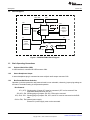
1
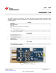
User's Guide
SLEU114 – May 2011
PCM270xEVM-U
This user's guide contains information on the setup, operation, and construction of the PCM270xEVM-U,
an evaluation module (EVM) for digital-to-analog converters (DACs) PCM2704 and PCM2705.
1
2
Contents
Description ...................................................................................................................
1.1
Related Documentation From Texas Instruments .............................................................
1.2
Block Diagram ......................................................................................................
1.3
Basic Operating Connections ....................................................................................
Schematic, BOM, and Printed-Circuit Board ............................................................................
2.1
PCM270xEVM-U Schematic ......................................................................................
2.2
PCM270xEVM-U Parts List (BOM) ..............................................................................
2.3
PCM270xEVM-U Printed-Circuit Board .........................................................................
1
1
2
2
4
4
5
6
List of Figures
1
PCM270xEVM-U Block Diagram.......................................................................................... 2
2
PCM270xEVM-U Circuit Diagram
3
PCM270xEVM-U Silkscreen ............................................................................................... 6
4
PCM270xEVM-U—Top View .............................................................................................. 6
5
PCM270xEVM-U—Bottom View .......................................................................................... 7
........................................................................................
4
List of Tables
1
1
Bill of Materials .............................................................................................................. 5
Description
The PCM270xEVM-U is an evaluation board for the USB interface DACs PCM2704 (DEM-PCM2704) and
PCM2705 (DEM-PCM2705).
A USB connector is mounted on the PCM270xEVM-U. This connector allows a customer to evaluate DAC
performance by connecting a USB interface to it.
By the use of jumper settings on the board, the PCM270xEVM-U can be operated either from USB bus
power or from an external 5-V power supply.
The PCM270xEVM-U outputs a stereo audio signal for headphones at stereo minijack CN2 (PD = 12 mW
at RL = 32 Ω), and an S/PDIF digital interface output at optical Toslink™ connector U4.
The PCM270xEVM-U is fully compliant with the USB 1.1 specification with full-speed transceiver format.
1.1
Related Documentation From Texas Instruments
PCM2704, PCM2705, PCM2706, PCM2707 Stereo Audio DAC With USB Interface, Single-Ended
Headphone Output and S/PDIF Output data sheet (SLES081)
Toslink is a trademark of Kabushiki Kaisha Toshiba DBA Toshiba Corporation.
All other trademarks are the property of their respective owners.
SLEU114 – May 2011
Submit Documentation Feedback
PCM270xEVM-U
Copyright © 2011, Texas Instruments Incorporated
1
Description
1.2
www.ti.com
Block Diagram
SW1–SW3
CN1
SPI(PCM2705)
HID
CN4
U3
CN2
EXT ROM
USB bus
interface
12-MHz
XTAL
Stereo
minijack
headphone
output
PCM2704
PCM2705
U4
U5
BUS/SELF power control
S/PDIF
output
TOTX141P
TM2
JP1–JP11
TM1
3.3-V reg
CN3
GND
+5 V
B0295-01
Figure 1. PCM270xEVM-U Block Diagram
1.3
1.3.1
Basic Operating Connections
Universal Serial Bus (USB)
A USB interface is connected to USB connector CN4.
1.3.2
Stereo Headphone Output
A stereo headphone plug is connected to stereo minijack audio output connector CN2.
1.3.3
Bus-Power/Self-Power Selection
Operation in the bus-powered or self-powered mode is user selectable, chosen by jumper plug settings on
the board. The default setting is self-powered operation.
Bus-Powered
JP1, (JP7): Shorting plug of jumper JP1 must be connected. (JP7 can be removed if the
application draws less than 100 mA.)
JP2–JP6, JP8: Shorting plugs of jumpers JP2–JP6, JP8 must be removed.
JP9, JP10, JP11: Shorting plugs of jumpers JP9, JP10, and JP11 must be connected on the BUS
side.
CN3 or TM1, TM2 external power supply:
External 5-V power supply must not be connected.
2
PCM270xEVM-U
Copyright © 2011, Texas Instruments Incorporated
SLEU114 – May 2011
Submit Documentation Feedback
Description
www.ti.com
Self-Powered (default setting)
JP1: Shorting plug of jumper JP1 must be removed.
JP2–JP8: Shorting plugs of jumpers JP2–JP8 must be connected.
JP9, JP10, JP11: Shorting plugs of jumpers JP9, JP10, and JP11 must be connected on the SELF
side.
CN3 or TM1, TM2 external power supply:
External power supply must be connected either to CN3 or to TM1 and TM2.
(VCC = 4.5 V to 10 V. ICC = 30 mA typical, 70 mA maximum.) A 3.3-V regulator IC is
mounted to provide a 3.3-V power supply for PCM2704/2705 and logic circuitry on
the board from the external power supply.
In the case of self-powered operation, device is enabled when the USB interface is
connected and HOST is set to High.
1.3.4
SPI Interface (PCM2705)
An SPI interface (MS, MC, MD) for operational control of the PCM2705 can be connected at CN1.
1.3.5
Suspend
Suspend status is indicated at the SSPND pin of CN1.
1.3.6
S/PDIF Output
USB audio data input to the PCM2704/2705 is output in S/PDIF format. This electrical output is sent to
U4, which converts the S/PDIF signal into light for optical transmission.
SLEU114 – May 2011
Submit Documentation Feedback
PCM270xEVM-U
Copyright © 2011, Texas Instruments Incorporated
3
4
GND
1uF
GND
C12
GND
Vdd
6
1
2
SHIELD
GND
VCC
U4
INPUT
0.01uF
C13
3
GND
AT24C64N-10SI-2.7TR
5
3
4
8
7
U3
1
2
0.01uF
C11
JP10
PCM270xEVM-U
Copyright © 2011, Texas Instruments Incorporated
Vdd
3
10Mohms
R18
2
GND GND
1uF
GND
1
JP11
1.5Kohms
R2
27ohms
SHIELD
SIGNAL
2
1
3
1
2
3
1.5Kohms
1
1
10ohms
1uF
GND
1Mohms
R15
GND
C1
10uF
1
2
23
6
1
VIN VOUT
GND
15
14
3
16
13
10uF
0.1uF
15pF
C2
1.5Kohms
0.022uF
10uF
16ohms
GND
GND
3
1
3
3
1
1
1.5Kohms
22Kohms
Vdd
1uF
C8
GND
GND
GND
GND
GND
C17
GND
+
GND
1Mohms
R16
17
18
19
20
21
12
11
10
9
8
22
24
5
7
26
2
28
27
25
U2
U1
1Mohms
R1
X1
3
1
4
2
C16
GND
+
15pF
GND
GND
R17
1uF
GND
JP9
Vdd
Vdd
SHUNT
CN3
27ohms
1.5Kohms
16ohms
2
GND
0.022uF
1uF
2
2
1.5Kohms
10Kohms
1.5Kohms
C15
100uF
C14
100uF
Vdd
GND GND
10Kohms
Vdd
1.5Kohms
1.5Kohms
6
5
4
3
2
1
CN1
GND
1
Left
Right
3
2
Case
CN2
2.1
+
2
+
1
2
3
Vdd
Schematic, BOM, and Printed-Circuit Board
www.ti.com
Schematic, BOM, and Printed-Circuit Board
This chapter presents the PCM270xEVM-U printed-circuit board and schematic.
PCM270xEVM-U Schematic
Figure 2. PCM270xEVM-U Circuit Diagram
SLEU114 – May 2011
Submit Documentation Feedback
Shield
Schematic, BOM, and Printed-Circuit Board
www.ti.com
2.2
PCM270xEVM-U Parts List (BOM)
Table 1. Bill of Materials
Item
QTY
MFG
MFG Part#
REF DES
Description
Value or Function
REF
–
PCM2704/2705 EVMA
–
ASSEMBLY
–
REF
–
PCM2704/2705 EVMA
–
SCHEMATIC
–
One Source
Group
PCM2704/2705 EVMA
–
FABRICATION
–
–
ARTWORK
–
1
PCM2704/2705 EVMA
–
1
4
2031
SO1, SO2, SO3, SO4
STANDOFF,4-40,1.0INx3/16IN,ALUM RND F-F
2
3
26630301RP2
JP9, JP10, JP11
HEADER 3 PIN, PCB 2.0MM ROHS
3
1
26630601RP2
CN1
HEADER 6 PIN, PCB 2.0MM ROHS
4
1
RAPC722X
CN3
JACK MINI-PWR THRU-RA 2,1ID/5.5OD 5A ROHS
5
1
STX-3000
CN2
JACK,MINI-STEREO,ROHS
6
1
TC7SZ08F
U5
2-Input AND Gate
7
1
TOTX141P
U4
TOSLINK TRANSMITTER 3.3V 15MB SHUTTER
ROHS
8
6
GRM185R61A105KE36D
C3, C4, C5, C6, C7, C12
603
CAP SMD0603 CERM 1.0UFD 10V 10% X5R
ROHS
9
1
GRM21BR71A106KE51LVSA
C8
805
CAP SMD0805 CERM 10UFD 10V10% X7R ROHS
10
1
3750-0
TM2
Black
BINDING POST, BLACK 60V/15A GOLD ROHS
11
1
PANASONIC
ECQ-B1H104JF
C18
CAP,RAD,POLY
CAP,THU,POLYES-FILM,0.1µF,50V,5%,85C
12
2
MURATA
GRM39X7R223K16V
C9, C10
CAP,SMT,0603
CAPACITOR,SMT,0603,CERAMIC,16V,10%,.022µ
F
13
2
MURATA
GRM40COG150J50V
C1, C2
CAP,SMT,0805
50V,±5%,15pF
14
2
MURATA
GRM40X7R103K50V
C11, C13
CAP,SMT,0805
50V,10%,.010µF
15
2
PANASONIC
EEVFC0J101P
C14, C15
CAPACITOR,SMT,ELEC
CAPACITOR,SMT,ELEC,100uF,6.3V,20%,
–40~105°C
16
1
ASSMANN
ELEC
A-USBS-B-R
CN4
CONNECTOR,THU,4P
CONNECTOR,THU,4P,USB RECEPTACLE,TYPE
B, PCB MOUNT
17
1
ECS
ECS-120-18-5P
X1
CRYSTAL,SMT,2P
XTL,SMT,12.000MHz,18pF,Fund,50ppm,-10~70°C
18
3
G12AP-RO
SW1, SW2, SW3
G12AP
SWITCH THRU SPDT STRAIGHT ULTRA
MINIATURE ROHS
19
8
SAMTEC
TSW-101-07-G-D
JP1, JP2, JP3, JP4, JP5, JP6,
JP7, JP8
HEADER,THU
HEADER,THU,2P,2X1,MALE,DUAL
ROW,100LS,100TL
20
1
ATMEL
AT24C64N-10SI-2.7TR
U3
IC,SMT,8P
2 WIRE SERIAL EEPROM
21
1
PANASONIC
ELJFA100KJ/F
L1
INDUCTOR,SMT
10.0µH
22
2
ECA1CM100
C16, C17
M
CAP ALUM ELEC M RADIAL 10UFD 16V 20%
ROHS
23
2
VISHAY
CRCW08051002F
R19, R20
RES,SMT,0805
RESISTOR,SMT,0805,THICK FILM,1%,1/8W,10.0K
24
3
VISHAY
CRCW08051004F
R1, R15, R16
RES,SMT,0805
RESISTER,SMT,0805,THICK FILM,1%,1/8W,1.00M
25
1
VISHAY
CRCW080510R0F
R17
RES,SMT,0805
RESISTER,SMT,0805,THICK FILM,1%,1/8W,10.0 Ω
26
9
VISHAY
CRCW08051501F
R2, R5, R6, R7, R10, R11, R12,
R13, R14
RES,SMT,0805
RESISTER,SMT,0805,THICK FILM,1%,1/8W,1.50K
27
1
PANASONIC
ERJ-6GEYJ106V
R18
RES,SMT,0805
RESISTOR,SMT,0805,THICK FILM,10M,5%,1/8W
28
2
PANASONIC
ERJ-6GEYJ160V
R8, R9
RES,SMT,0805
RESISTOR,SMT,0805,THICK FILM,5%,1/8W,16
29
2
PANASONIC
ERJ-6GEYJ270V
R3, R4
RES,SMT,0805
RESISTOR,SMT,0805,THICK FILM,5%,1/8W,27
30
1
PANASONIC
ERA-6YEB223V
R21
RES,SMT,2P
RESISTOR,SMT,0805,22K,0.1%,1/10W,25ppm
31
1
3750-2
TM1
Red
BINDING POST, RED 60V/15A GOLD ROHS
32
1
REG1117-3.3
U2
SOT223-DCY
VOLT REG 3.3V 800mA SOT223-DCY ROHS
33
1
PCM2705DB
U1
SSOP28-DB
STEREO AUDIO DAC W/USB SE
HEADPHONE/SPDIF OUT SSOP28-DB ROHS
REF
NOTE: ASTERISK(*) NEXT TO PART MANUFACTURER'S NAME DENOTES POSSIBLE LONG LEAD TIME ITEM.
SLEU114 – May 2011
Submit Documentation Feedback
PCM270xEVM-U
Copyright © 2011, Texas Instruments Incorporated
5
Schematic, BOM, and Printed-Circuit Board
2.3
www.ti.com
PCM270xEVM-U Printed-Circuit Board
SO3
R7
SW1
R6
SW2
R5
CN1
SW3
SO2
TM2
CN3
TM1
C16
+
U2
X1
C7
C14
CN2
R1
U1
C15
C9 R8
JP7
+
C1
R9 C10
U3
JP4
R16
C6
C3
C2
R10 R11
C18
R19
+
R20
R18
TPGND
JP1
U4
JP2
R15
JP8
C5
+
R3
C4
C8
R2
R13
R12
C11 C12
CN4
JP5
R14
L1
SO1
JP6
R21
+
C13
U5
R4
C17
+
JP11
JP10
PSEL
JP3
SO4
JP9
R17
Figure 3. PCM270xEVM-U Silkscreen
SO3
R7
SW1
R6
SW2
R5
CN1
SW3
SO2
TM2
C17
U2
C5
R21
X1
C7
C14
C15
CN2
C9 R8
U1
R1
R16
C1
R10 R11
R9 C10
JP7
C11 C12
C18
R19
C2
JP4
R20
R18
TPGND
JP1
U4
PSEL
JP2
R15
C3
JP8
C4
C6
R3
JP5
C8
R4
R13
R12
L1
CN4
JP6
R14
U3
C13
U5
R2
C16
JP11
JP10
SO1
CN3
TM1
JP3
JP9
SO4
R17
Figure 4. PCM270xEVM-U—Top View
6
PCM270xEVM-U
Copyright © 2011, Texas Instruments Incorporated
SLEU114 – May 2011
Submit Documentation Feedback
www.ti.com
Schematic, BOM, and Printed-Circuit Board
Figure 5. PCM270xEVM-U—Bottom View
SLEU114 – May 2011
Submit Documentation Feedback
PCM270xEVM-U
Copyright © 2011, Texas Instruments Incorporated
7
Evaluation Board/Kit Important Notice
Texas Instruments (TI) provides the enclosed product(s) under the following conditions:
This evaluation board/kit is intended for use for ENGINEERING DEVELOPMENT, DEMONSTRATION, OR EVALUATION
PURPOSES ONLY and is not considered by TI to be a finished end-product fit for general consumer use. Persons handling the
product(s) must have electronics training and observe good engineering practice standards. As such, the goods being provided are
not intended to be complete in terms of required design-, marketing-, and/or manufacturing-related protective considerations,
including product safety and environmental measures typically found in end products that incorporate such semiconductor
components or circuit boards. This evaluation board/kit does not fall within the scope of the European Union directives regarding
electromagnetic compatibility, restricted substances (RoHS), recycling (WEEE), FCC, CE or UL, and therefore may not meet the
technical requirements of these directives or other related directives.
Should this evaluation board/kit not meet the specifications indicated in the User’s Guide, the board/kit may be returned within 30
days from the date of delivery for a full refund. THE FOREGOING WARRANTY IS THE EXCLUSIVE WARRANTY MADE BY
SELLER TO BUYER AND IS IN LIEU OF ALL OTHER WARRANTIES, EXPRESSED, IMPLIED, OR STATUTORY, INCLUDING
ANY WARRANTY OF MERCHANTABILITY OR FITNESS FOR ANY PARTICULAR PURPOSE.
The user assumes all responsibility and liability for proper and safe handling of the goods. Further, the user indemnifies TI from all
claims arising from the handling or use of the goods. Due to the open construction of the product, it is the user’s responsibility to
take any and all appropriate precautions with regard to electrostatic discharge.
EXCEPT TO THE EXTENT OF THE INDEMNITY SET FORTH ABOVE, NEITHER PARTY SHALL BE LIABLE TO THE OTHER
FOR ANY INDIRECT, SPECIAL, INCIDENTAL, OR CONSEQUENTIAL DAMAGES.
TI currently deals with a variety of customers for products, and therefore our arrangement with the user is not exclusive.
TI assumes no liability for applications assistance, customer product design, software performance, or infringement of
patents or services described herein.
Please read the User’s Guide and, specifically, the Warnings and Restrictions notice in the User’s Guide prior to handling the
product. This notice contains important safety information about temperatures and voltages. For additional information on TI’s
environmental and/or safety programs, please contact the TI application engineer or visit www.ti.com/esh.
No license is granted under any patent right or other intellectual property right of TI covering or relating to any machine, process, or
combination in which such TI products or services might be or are used.
FCC Warning
This evaluation board/kit is intended for use for ENGINEERING DEVELOPMENT, DEMONSTRATION, OR EVALUATION
PURPOSES ONLY and is not considered by TI to be a finished end-product fit for general consumer use. It generates, uses, and
can radiate radio frequency energy and has not been tested for compliance with the limits of computing devices pursuant to part 15
of FCC rules, which are designed to provide reasonable protection against radio frequency interference. Operation of this
equipment in other environments may cause interference with radio communications, in which case the user at his own expense
will be required to take whatever measures may be required to correct this interference.
EVM Warnings and Restrictions
It is important to operate this EVM within the input voltage range of 5 V and the output voltage range of 5 V .
Exceeding the specified input range may cause unexpected operation and/or irreversible damage to the EVM. If there are
questions concerning the input range, please contact a TI field representative prior to connecting the input power.
Applying loads outside of the specified output range may result in unintended operation and/or possible permanent damage to the
EVM. Please consult the EVM User's Guide prior to connecting any load to the EVM output. If there is uncertainty as to the load
specification, please contact a TI field representative.
During normal operation, some circuit components may have case temperatures greater than 55°C. The EVM is designed to
operate properly with certain components above 55°C as long as the input and output ranges are maintained. These components
include but are not limited to linear regulators, switching transistors, pass transistors, and current sense resistors. These types of
devices can be identified using the EVM schematic located in the EVM User's Guide. When placing measurement probes near
these devices during operation, please be aware that these devices may be very warm to the touch.
Mailing Address: Texas Instruments, Post Office Box 655303, Dallas, Texas 75265
Copyright © 2011, Texas Instruments Incorporated
IMPORTANT NOTICE
Texas Instruments Incorporated and its subsidiaries (TI) reserve the right to make corrections, modifications, enhancements, improvements,
and other changes to its products and services at any time and to discontinue any product or service without notice. Customers should
obtain the latest relevant information before placing orders and should verify that such information is current and complete. All products are
sold subject to TI’s terms and conditions of sale supplied at the time of order acknowledgment.
TI warrants performance of its hardware products to the specifications applicable at the time of sale in accordance with TI’s standard
warranty. Testing and other quality control techniques are used to the extent TI deems necessary to support this warranty. Except where
mandated by government requirements, testing of all parameters of each product is not necessarily performed.
TI assumes no liability for applications assistance or customer product design. Customers are responsible for their products and
applications using TI components. To minimize the risks associated with customer products and applications, customers should provide
adequate design and operating safeguards.
TI does not warrant or represent that any license, either express or implied, is granted under any TI patent right, copyright, mask work right,
or other TI intellectual property right relating to any combination, machine, or process in which TI products or services are used. Information
published by TI regarding third-party products or services does not constitute a license from TI to use such products or services or a
warranty or endorsement thereof. Use of such information may require a license from a third party under the patents or other intellectual
property of the third party, or a license from TI under the patents or other intellectual property of TI.
Reproduction of TI information in TI data books or data sheets is permissible only if reproduction is without alteration and is accompanied
by all associated warranties, conditions, limitations, and notices. Reproduction of this information with alteration is an unfair and deceptive
business practice. TI is not responsible or liable for such altered documentation. Information of third parties may be subject to additional
restrictions.
Resale of TI products or services with statements different from or beyond the parameters stated by TI for that product or service voids all
express and any implied warranties for the associated TI product or service and is an unfair and deceptive business practice. TI is not
responsible or liable for any such statements.
TI products are not authorized for use in safety-critical applications (such as life support) where a failure of the TI product would reasonably
be expected to cause severe personal injury or death, unless officers of the parties have executed an agreement specifically governing
such use. Buyers represent that they have all necessary expertise in the safety and regulatory ramifications of their applications, and
acknowledge and agree that they are solely responsible for all legal, regulatory and safety-related requirements concerning their products
and any use of TI products in such safety-critical applications, notwithstanding any applications-related information or support that may be
provided by TI. Further, Buyers must fully indemnify TI and its representatives against any damages arising out of the use of TI products in
such safety-critical applications.
TI products are neither designed nor intended for use in military/aerospace applications or environments unless the TI products are
specifically designated by TI as military-grade or "enhanced plastic." Only products designated by TI as military-grade meet military
specifications. Buyers acknowledge and agree that any such use of TI products which TI has not designated as military-grade is solely at
the Buyer's risk, and that they are solely responsible for compliance with all legal and regulatory requirements in connection with such use.
TI products are neither designed nor intended for use in automotive applications or environments unless the specific TI products are
designated by TI as compliant with ISO/TS 16949 requirements. Buyers acknowledge and agree that, if they use any non-designated
products in automotive applications, TI will not be responsible for any failure to meet such requirements.
Following are URLs where you can obtain information on other Texas Instruments products and application solutions:
Products
Applications
Audio
www.ti.com/audio
Communications and Telecom www.ti.com/communications
Amplifiers
amplifier.ti.com
Computers and Peripherals
www.ti.com/computers
Data Converters
dataconverter.ti.com
Consumer Electronics
www.ti.com/consumer-apps
DLP® Products
www.dlp.com
Energy and Lighting
www.ti.com/energy
DSP
dsp.ti.com
Industrial
www.ti.com/industrial
Clocks and Timers
www.ti.com/clocks
Medical
www.ti.com/medical
Interface
interface.ti.com
Security
www.ti.com/security
Logic
logic.ti.com
Space, Avionics and Defense
www.ti.com/space-avionics-defense
Power Mgmt
power.ti.com
Transportation and
Automotive
www.ti.com/automotive
Microcontrollers
microcontroller.ti.com
Video and Imaging
www.ti.com/video
RFID
www.ti-rfid.com
Wireless
www.ti.com/wireless-apps
RF/IF and ZigBee® Solutions
www.ti.com/lprf
TI E2E Community Home Page
e2e.ti.com
Mailing Address: Texas Instruments, Post Office Box 655303, Dallas, Texas 75265
Copyright © 2011, Texas Instruments Incorporated