1
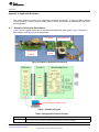
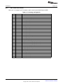
User's Guide
SLVU844 – February 2013
DRV3204-Q1 EVM
This document is a supplement to the DRV3204-Q1 data sheet (SLVSBT3). It details the hardware
implementation of DRV3204-Q1 evaluation module (EVM). This document does not cover the motor-driver
application and the software.
Section 1 and Section 2 list the hardware descriptions of the EVM. Appendix A details getting started with
the evaluation, and Appendix B describes the 3.3-V interface (I/F) board.
Contents
1
Overview .....................................................................................................................
2
Connectors and Switches ..................................................................................................
Appendix A
Application Evaluation .............................................................................................
Appendix B
I/F Board ............................................................................................................
1
4
7
9
List of Figures
1
DRV3204EVM Board Layout (Front Side) ............................................................................... 2
2
DRV3204EVM Board Layout (Back Side) ............................................................................... 2
3
DRV3204EVM Block Diagram............................................................................................. 3
4
Device Enable Switch ...................................................................................................... 5
5
Watchdog Disable Switch .................................................................................................. 5
6
Example of Evaluation Environment...................................................................................... 7
7
EVM Block Diagram ........................................................................................................ 7
8
TI Code Composer Studio Screen Capture ............................................................................. 8
9
Board Layout (Front Side) ................................................................................................. 9
10
Board Layout (Back Side).................................................................................................. 9
List of Tables
1
Power Connectors .......................................................................................................... 4
2
Motor Outputs ............................................................................................................... 4
3
Analog and Digital I/O ...................................................................................................... 4
4
Device Enable Switch ...................................................................................................... 5
5
Watchdog Disable Switch .................................................................................................. 6
6
Debugging Environment Example ........................................................................................ 7
7
VCC Output Connector ..................................................................................................... 9
8
3.3-V Analog and Digital I/O ............................................................................................. 10
1
Overview
1.1
Introduction
The DRV3204EVM is an application board to evaluate the DRV3204-Q1 device. The DRV3204-Q1 device
is a field effect transistor (FET) pre-driver designed for a 3-phase brushless DC motor control. The EVM
consists of the DRV3204-Q1 device, six N-channel MOSFETs, and passive devices. The DRV3204EVM
has a 5-V level interface to communicate with an external micro-controller unit (MCU). A 3.3-V I/F board is
also provided to support the 3.3-V MCU.
SLVU844 – February 2013
Submit Documentation Feedback
DRV3204-Q1 EVM
Copyright © 2013, Texas Instruments Incorporated
1
Overview
1.2
www.ti.com
Block Diagram
SW2 : Watchdog Disable Switch
SW1 : Device Enable Switch
LED : Power Status
CN1 : Power Connecter
CN2 : Motor Output
CN3 : Analog and Digital I/Os
Figure 1. DRV3204EVM Board Layout (Front Side)
PNP Transistor for VCC
FETs
Figure 2. DRV3204EVM Board Layout (Back Side)
2
DRV3204-Q1 EVM
SLVU844 – February 2013
Submit Documentation Feedback
Copyright © 2013, Texas Instruments Incorporated
Overview
www.ti.com
Test Pins
Switch
LED
Power
Connector
DRV3204
J1
Motor
Driver
Figure 3. DRV3204EVM Block Diagram
1.2.1
Power and Communication Connectors
The EVM offers terminal blocks for the application of power and motor outputs, as well as digital
input/output (I/O) and communication. This section briefly describes the functions. The pin assignments
are described in Section 2.
1.2.1.1
Power Connector
The VB power rail (typically 12 V) must be externally supplied. The power for the external MCU and other
analog and digital functions are supplied by the regulator implemented in the DRV3204-Q1 device.
1.2.1.2
Motor Outputs
A brushless DC Motor is connected to the EVM through the motor outputs.
1.2.1.3
Analog and Digital I/O
The analog and digital I/O and SPI communication of the DRV3204-Q1 can be used through the
connector.
1.2.2
LED
The LED turns on when the DRV3204EVM power is supplied.
1.2.3
Switch
Switch1 is connected to the enable input (ENABLE) pin of the DRV3204-Q1. DRV3204-Q1 is enabled by
turning this switch ON. Switch3 is for disabling the watchdog function. When you want to disable the
watchdog function, this switch must be set to the RES position.
1.2.4
FETs
Six N-channel MOSFETs are implemented on the board to drive the brushless DC motor. A 10-A
maximum brushless DC motor can be evaluated using this EVM board.
SLVU844 – February 2013
Submit Documentation Feedback
DRV3204-Q1 EVM
Copyright © 2013, Texas Instruments Incorporated
3
Connectors and Switches
1.2.5
www.ti.com
Test Pins
The DRV3204-Q1 pins are brought out to the test pin or test through-hole. For each test pin, a label on
the silkscreen identifies the signal. Access the signals by using 14 through-holes, marked as J1.
2
Connectors and Switches
This section describes the pin assignment of the connectors and switches.
2.1
2.1.1
Connectors
CN1 – B3P-VH-FB-B(LF)(SN) (JST)
Table 1. Power Connectors
Pin#
2.1.2
Name
Description
1
VB
External power supply (typ 12-V, max 10 A)
2
NC
No connection
3
GND
Base ground (B-GND)
CN2 – B5P-VH-FB-B(LF)(SN) (JST)
Table 2. Motor Outputs
2.1.3
Pin#
Name
Description
1
Motor1
Motor terminal 1
2
NC
3
Motor2
4
NC
5
Motor3
No Connection
Motor terminal 2
No Connection
Motor terminal 3
CN3 – FCN-365J032-AU (Fujitsu Component)
Table 3. Analog and Digital I/O
4
Pin#
Name
Description
A1
PMV1
Phase comparator output 1
B1
PMV2
Phase comparator output 2
A2
PMV3
Phase comparator output 3
B2
PSS1
Sample and hold control signal input 1 (not used)
A3
PSS2
Sample and hold control signal input 2 (not used)
B3
PSS3
Sample and hold control signal input 3 (not used)
A4
CS
B4
DOUT
SPI chip select signal input
SPI data signal output
A5
SCK
SPI clock signal input
B5
DIN
SPI data signal input
A6
CTLEN
Pre-driver parallel enable input (not used)
B6
CTLWL
Pre-driver parallel input
A7
CTLWH
Pre-driver parallel input
B7
CTLVL
Pre-driver parallel input
A8
CTLVH
Pre-driver parallel input
B8
CTLUL
Pre-driver parallel input
DRV3204-Q1 EVM
SLVU844 – February 2013
Submit Documentation Feedback
Copyright © 2013, Texas Instruments Incorporated
Connectors and Switches
www.ti.com
Table 3. Analog and Digital I/O (continued)
2.2
2.2.1
Pin#
Name
A9
CTLUH
Description
Pre-driver parallel input
B9
RES
Reset output
A10
PRN
Watchdog timer pulse input
B10
FAULT
Diagnosis output
A11
OVCR
Overcurrent reset input (not used)
B11
NC
A12
CANRX
No connection
CAN digital receive data output (not used)
B12
CANTX
CAN digital transmit data input (not used)
A13
NC
No Connection
B13
PTV1
Phase output 1
A14
PTV2
Phase output 2
B14
PTV3
Phase output 3
A15
GND
Ground
B15
ALV
Motor current sense amp output
A16
GND
Ground
B16
VCC
5-V VCC supply output
Switches
SW1
EVM
ON
SW
OFF
Figure 4. Device Enable Switch
Table 4. Device Enable Switch
2.2.2
Switch
Description
ON
DRV3204 ENABLE = VB
DRV3204-Q1 is enabled
OFF
DRV3204 ENABLE = OPEN
DRV3204-Q1 is disabled
SW2
EVM
SW2
RES
PRN
Figure 5. Watchdog Disable Switch
SLVU844 – February 2013
Submit Documentation Feedback
DRV3204-Q1 EVM
Copyright © 2013, Texas Instruments Incorporated
5
Connectors and Switches
www.ti.com
Table 5. Watchdog Disable Switch
6
Switch
Description
PRN
Watchdog function is enabled.
It is controlled through the CN3 by MCU.
RES
Watchdog function is disabled.
DRV3204-Q1 EVM
SLVU844 – February 2013
Submit Documentation Feedback
Copyright © 2013, Texas Instruments Incorporated
www.ti.com
Appendix A Application Evaluation
This section gives an overview of an application evaluation environment. It uses an F28035 (C2000)
Control Card and TI Code Composer Studio (CCS) to control and monitor the DRV3204-Q1 and motordriver application.
A.1
Example of Evaluation Environment
Figure 6 shows a typical environment to evaluate the brushless DC motor system, Figure 7 shows the
block diagram, and Table 6 lists the components.
I/F Board
DRV3204EVM
Control Card
Motor
(F28035)
Figure 6. Example of Evaluation Environment
TI Code Composer Studio (CCS)
Figure 7. EVM Block Diagram
Table 6. Debugging Environment Example
Component
Description
CCS
CCS is the integrated development environment (IDE) for TI’s micro-controllers. It provides a compiler of the
user’s code, a source code editor, a project build environment and real-time debugger.
SLVU844 – February 2013
Submit Documentation Feedback
Application Evaluation
Copyright © 2013, Texas Instruments Incorporated
7
Example of Evaluation Environment
www.ti.com
Table 6. Debugging Environment Example (continued)
Component
Description
Control CARD
The Piccolo F28035 Control CARD is a TI 32-bit CPU suitable for motor-driver or power management
applications.
I/F board
The I/F board converts the I/O voltage level between the Control CARD (3.3 V) and the DRV3204EVM (5 V).
MOTOR
A 3-phase brushless DC motor
Power supply
A 12-V power supply to EVM board
Real Time
Debug
Commutation
Pointer
AD Converted
Data
Figure 8. TI Code Composer Studio Screen Capture
The TI CCS offers real-time debugging with a C2000 MCU. It controls C2000 parameters or displays a
motor-control status.
8
Application Evaluation
SLVU844 – February 2013
Submit Documentation Feedback
Copyright © 2013, Texas Instruments Incorporated
www.ti.com
Appendix B I/F Board
B.1
I/F Board Overview
CN4 : 3.3-V Analog and Digital I/Os
Level Shifters : 3.3 V ó 5.0 V
CN5 : VCC Output Connector
CN3 : 5-V Analog and Digital I/Os
CN2 : VCC Output Connector
Figure 9. Board Layout (Front Side)
3.3-V Regulator
Figure 10. Board Layout (Back Side)
B.2
B.2.1
Connectors
CN1
Not used
B.2.2
CN2 and CN5 – B3B-XH-A(LF)(SN) (JST)
CN2 and CN5 are 5-V power supplies to components on the board or external devices.
Table 7. VCC Output Connector
B.2.3
Pin#
Name
Description
1
VCC
VCC power supply output
2
NC
No connection
3
GND
Ground
CN3 – FCN-365P032-AU (Fujitsu Component)
CN3 is a 5-V voltage level I/F connector, and It is connected on the DRV3204EVM.
Refer to Table 3.
SLVU844 – February 2013
Submit Documentation Feedback
I/F Board
Copyright © 2013, Texas Instruments Incorporated
9
Connectors
B.2.4
www.ti.com
CN4 – XG4C-3031 (omrom)
CN4 is a 3.3-V voltage level I/F connector, and it is used on the C2000 Control CARD.
Table 8. 3.3-V Analog and Digital I/O
10
Pin#
Name
Description
1
GND
Ground
2
ISCOMP
Current comparator output
3
ALV
Motor current sense amp output
4
PTV3
Phase amplifier output 3
5
PTV2
Phase amplifier output 2
6
PTV1
Phase amplifier output 1
7
NC
No connection
8
PRN
Pulse input
9
CTLUH
Pre-driver parallel input
10
CTLUL
Pre-driver parallel input
11
CTLVH
Pre-driver parallel input
12
CTLVL
Pre-driver parallel input
13
CTLWH
Pre-driver parallel input
14
CTLWL
Pre-driver parallel input
15
CTLEN
Pre-driver parallel enable input
16
DIN
SPI data signal input
17
SCK
SPI clock signal input
18
CS
SPI chip select signal input
19
PSS3
Sample and hold control signal input 3 (not used)
20
PSS2
Sample and hold control signal input 2 (not used)
21
PSS1
Sample and hold control signal input 1 (not used)
22
OVCR
Overcurrent reset input (not used)
23
CANTX
CAN digital input (not used)
24
CANRX
CAN digital output (not used)
25
FAULT
Diagnosis output
26
RES
Reset output
27
DOUT
SPI data signal output
28
PMV3
Phase comparator output 3
29
PMV2
Phase comparator output 2
30
PMV1
Phase comparator output 1
I/F Board
SLVU844 – February 2013
Submit Documentation Feedback
Copyright © 2013, Texas Instruments Incorporated
EVALUATION BOARD/KIT/MODULE (EVM) ADDITIONAL TERMS
Texas Instruments (TI) provides the enclosed Evaluation Board/Kit/Module (EVM) under the following conditions:
The user assumes all responsibility and liability for proper and safe handling of the goods. Further, the user indemnifies TI from all claims
arising from the handling or use of the goods.
Should this evaluation board/kit not meet the specifications indicated in the User’s Guide, the board/kit may be returned within 30 days from
the date of delivery for a full refund. THE FOREGOING LIMITED WARRANTY IS THE EXCLUSIVE WARRANTY MADE BY SELLER TO
BUYER AND IS IN LIEU OF ALL OTHER WARRANTIES, EXPRESSED, IMPLIED, OR STATUTORY, INCLUDING ANY WARRANTY OF
MERCHANTABILITY OR FITNESS FOR ANY PARTICULAR PURPOSE. EXCEPT TO THE EXTENT OF THE INDEMNITY SET FORTH
ABOVE, NEITHER PARTY SHALL BE LIABLE TO THE OTHER FOR ANY INDIRECT, SPECIAL, INCIDENTAL, OR CONSEQUENTIAL
DAMAGES.
Please read the User's Guide and, specifically, the Warnings and Restrictions notice in the User's Guide prior to handling the product. This
notice contains important safety information about temperatures and voltages. For additional information on TI's environmental and/or safety
programs, please visit www.ti.com/esh or contact TI.
No license is granted under any patent right or other intellectual property right of TI covering or relating to any machine, process, or
combination in which such TI products or services might be or are used. TI currently deals with a variety of customers for products, and
therefore our arrangement with the user is not exclusive. TI assumes no liability for applications assistance, customer product design,
software performance, or infringement of patents or services described herein.
REGULATORY COMPLIANCE INFORMATION
As noted in the EVM User’s Guide and/or EVM itself, this EVM and/or accompanying hardware may or may not be subject to the Federal
Communications Commission (FCC) and Industry Canada (IC) rules.
For EVMs not subject to the above rules, this evaluation board/kit/module is intended for use for ENGINEERING DEVELOPMENT,
DEMONSTRATION OR EVALUATION PURPOSES ONLY and is not considered by TI to be a finished end product fit for general consumer
use. It generates, uses, and can radiate radio frequency energy and has not been tested for compliance with the limits of computing
devices pursuant to part 15 of FCC or ICES-003 rules, which are designed to provide reasonable protection against radio frequency
interference. Operation of the equipment may cause interference with radio communications, in which case the user at his own expense will
be required to take whatever measures may be required to correct this interference.
General Statement for EVMs including a radio
User Power/Frequency Use Obligations: This radio is intended for development/professional use only in legally allocated frequency and
power limits. Any use of radio frequencies and/or power availability of this EVM and its development application(s) must comply with local
laws governing radio spectrum allocation and power limits for this evaluation module. It is the user’s sole responsibility to only operate this
radio in legally acceptable frequency space and within legally mandated power limitations. Any exceptions to this are strictly prohibited and
unauthorized by Texas Instruments unless user has obtained appropriate experimental/development licenses from local regulatory
authorities, which is responsibility of user including its acceptable authorization.
For EVMs annotated as FCC – FEDERAL COMMUNICATIONS COMMISSION Part 15 Compliant
Caution
This device complies with part 15 of the FCC Rules. Operation is subject to the following two conditions: (1) This device may not cause
harmful interference, and (2) this device must accept any interference received, including interference that may cause undesired operation.
Changes or modifications not expressly approved by the party responsible for compliance could void the user's authority to operate the
equipment.
FCC Interference Statement for Class A EVM devices
This equipment has been tested and found to comply with the limits for a Class A digital device, pursuant to part 15 of the FCC Rules.
These limits are designed to provide reasonable protection against harmful interference when the equipment is operated in a commercial
environment. This equipment generates, uses, and can radiate radio frequency energy and, if not installed and used in accordance with the
instruction manual, may cause harmful interference to radio communications. Operation of this equipment in a residential area is likely to
cause harmful interference in which case the user will be required to correct the interference at his own expense.
FCC Interference Statement for Class B EVM devices
This equipment has been tested and found to comply with the limits for a Class B digital device, pursuant to part 15 of the FCC Rules.
These limits are designed to provide reasonable protection against harmful interference in a residential installation. This equipment
generates, uses and can radiate radio frequency energy and, if not installed and used in accordance with the instructions, may cause
harmful interference to radio communications. However, there is no guarantee that interference will not occur in a particular installation. If
this equipment does cause harmful interference to radio or television reception, which can be determined by turning the equipment off and
on, the user is encouraged to try to correct the interference by one or more of the following measures:
• Reorient or relocate the receiving antenna.
• Increase the separation between the equipment and receiver.
• Connect the equipment into an outlet on a circuit different from that to which the receiver is connected.
• Consult the dealer or an experienced radio/TV technician for help.
For EVMs annotated as IC – INDUSTRY CANADA Compliant
This Class A or B digital apparatus complies with Canadian ICES-003.
Changes or modifications not expressly approved by the party responsible for compliance could void the user’s authority to operate the
equipment.
Concerning EVMs including radio transmitters
This device complies with Industry Canada licence-exempt RSS standard(s). Operation is subject to the following two conditions: (1) this
device may not cause interference, and (2) this device must accept any interference, including interference that may cause undesired
operation of the device.
Concerning EVMs including detachable antennas
Under Industry Canada regulations, this radio transmitter may only operate using an antenna of a type and maximum (or lesser) gain
approved for the transmitter by Industry Canada. To reduce potential radio interference to other users, the antenna type and its gain should
be so chosen that the equivalent isotropically radiated power (e.i.r.p.) is not more than that necessary for successful communication.
This radio transmitter has been approved by Industry Canada to operate with the antenna types listed in the user guide with the maximum
permissible gain and required antenna impedance for each antenna type indicated. Antenna types not included in this list, having a gain
greater than the maximum gain indicated for that type, are strictly prohibited for use with this device.
Cet appareil numérique de la classe A ou B est conforme à la norme NMB-003 du Canada.
Les changements ou les modifications pas expressément approuvés par la partie responsable de la conformité ont pu vider l’autorité de
l'utilisateur pour actionner l'équipement.
Concernant les EVMs avec appareils radio
Le présent appareil est conforme aux CNR d'Industrie Canada applicables aux appareils radio exempts de licence. L'exploitation est
autorisée aux deux conditions suivantes : (1) l'appareil ne doit pas produire de brouillage, et (2) l'utilisateur de l'appareil doit accepter tout
brouillage radioélectrique subi, même si le brouillage est susceptible d'en compromettre le fonctionnement.
Concernant les EVMs avec antennes détachables
Conformément à la réglementation d'Industrie Canada, le présent émetteur radio peut fonctionner avec une antenne d'un type et d'un gain
maximal (ou inférieur) approuvé pour l'émetteur par Industrie Canada. Dans le but de réduire les risques de brouillage radioélectrique à
l'intention des autres utilisateurs, il faut choisir le type d'antenne et son gain de sorte que la puissance isotrope rayonnée équivalente
(p.i.r.e.) ne dépasse pas l'intensité nécessaire à l'établissement d'une communication satisfaisante.
Le présent émetteur radio a été approuvé par Industrie Canada pour fonctionner avec les types d'antenne énumérés dans le manuel
d’usage et ayant un gain admissible maximal et l'impédance requise pour chaque type d'antenne. Les types d'antenne non inclus dans
cette liste, ou dont le gain est supérieur au gain maximal indiqué, sont strictement interdits pour l'exploitation de l'émetteur.
SPACER
SPACER
SPACER
SPACER
SPACER
SPACER
SPACER
SPACER
【Important Notice for Users of this Product in Japan】
】
This development kit is NOT certified as Confirming to Technical Regulations of Radio Law of Japan
If you use this product in Japan, you are required by Radio Law of Japan to follow the instructions below with respect to this product:
1.
2.
3.
Use this product in a shielded room or any other test facility as defined in the notification #173 issued by Ministry of Internal Affairs and
Communications on March 28, 2006, based on Sub-section 1.1 of Article 6 of the Ministry’s Rule for Enforcement of Radio Law of
Japan,
Use this product only after you obtained the license of Test Radio Station as provided in Radio Law of Japan with respect to this
product, or
Use of this product only after you obtained the Technical Regulations Conformity Certification as provided in Radio Law of Japan with
respect to this product. Also, please do not transfer this product, unless you give the same notice above to the transferee. Please note
that if you could not follow the instructions above, you will be subject to penalties of Radio Law of Japan.
Texas Instruments Japan Limited
(address) 24-1, Nishi-Shinjuku 6 chome, Shinjuku-ku, Tokyo, Japan
http://www.tij.co.jp
【ご使用にあたっての注】
本開発キットは技術基準適合証明を受けておりません。
本製品のご使用に際しては、電波法遵守のため、以下のいずれかの措置を取っていただく必要がありますのでご注意ください。
1.
2.
3.
電波法施行規則第6条第1項第1号に基づく平成18年3月28日総務省告示第173号で定められた電波暗室等の試験設備でご使用いただく。
実験局の免許を取得後ご使用いただく。
技術基準適合証明を取得後ご使用いただく。
なお、本製品は、上記の「ご使用にあたっての注意」を譲渡先、移転先に通知しない限り、譲渡、移転できないものとします。
上記を遵守頂けない場合は、電波法の罰則が適用される可能性があることをご留意ください。
日本テキサス・インスツルメンツ株式会社
東京都新宿区西新宿6丁目24番1号
西新宿三井ビル
http://www.tij.co.jp
SPACER
SPACER
SPACER
SPACER
SPACER
SPACER
SPACER
SPACER
SPACER
SPACER
SPACER
SPACER
SPACER
SPACER
SPACER
SPACER
EVALUATION BOARD/KIT/MODULE (EVM)
WARNINGS, RESTRICTIONS AND DISCLAIMERS
For Feasibility Evaluation Only, in Laboratory/Development Environments. Unless otherwise indicated, this EVM is not a finished
electrical equipment and not intended for consumer use. It is intended solely for use for preliminary feasibility evaluation in
laboratory/development environments by technically qualified electronics experts who are familiar with the dangers and application risks
associated with handling electrical mechanical components, systems and subsystems. It should not be used as all or part of a finished end
product.
Your Sole Responsibility and Risk. You acknowledge, represent and agree that:
1.
2.
3.
4.
You have unique knowledge concerning Federal, State and local regulatory requirements (including but not limited to Food and Drug
Administration regulations, if applicable) which relate to your products and which relate to your use (and/or that of your employees,
affiliates, contractors or designees) of the EVM for evaluation, testing and other purposes.
You have full and exclusive responsibility to assure the safety and compliance of your products with all such laws and other applicable
regulatory requirements, and also to assure the safety of any activities to be conducted by you and/or your employees, affiliates,
contractors or designees, using the EVM. Further, you are responsible to assure that any interfaces (electronic and/or mechanical)
between the EVM and any human body are designed with suitable isolation and means to safely limit accessible leakage currents to
minimize the risk of electrical shock hazard.
You will employ reasonable safeguards to ensure that your use of the EVM will not result in any property damage, injury or death, even
if the EVM should fail to perform as described or expected.
You will take care of proper disposal and recycling of the EVM’s electronic components and packing materials.
Certain Instructions. It is important to operate this EVM within TI’s recommended specifications and environmental considerations per the
user guidelines. Exceeding the specified EVM ratings (including but not limited to input and output voltage, current, power, and
environmental ranges) may cause property damage, personal injury or death. If there are questions concerning these ratings please contact
a TI field representative prior to connecting interface electronics including input power and intended loads. Any loads applied outside of the
specified output range may result in unintended and/or inaccurate operation and/or possible permanent damage to the EVM and/or
interface electronics. Please consult the EVM User's Guide prior to connecting any load to the EVM output. If there is uncertainty as to the
load specification, please contact a TI field representative. During normal operation, some circuit components may have case temperatures
greater than 60°C as long as the input and output are maintained at a normal ambient operating temperature. These components include
but are not limited to linear regulators, switching transistors, pass transistors, and current sense resistors which can be identified using the
EVM schematic located in the EVM User's Guide. When placing measurement probes near these devices during normal operation, please
be aware that these devices may be very warm to the touch. As with all electronic evaluation tools, only qualified personnel knowledgeable
in electronic measurement and diagnostics normally found in development environments should use these EVMs.
Agreement to Defend, Indemnify and Hold Harmless. You agree to defend, indemnify and hold TI, its licensors and their representatives
harmless from and against any and all claims, damages, losses, expenses, costs and liabilities (collectively, "Claims") arising out of or in
connection with any use of the EVM that is not in accordance with the terms of the agreement. This obligation shall apply whether Claims
arise under law of tort or contract or any other legal theory, and even if the EVM fails to perform as described or expected.
Safety-Critical or Life-Critical Applications. If you intend to evaluate the components for possible use in safety critical applications (such
as life support) where a failure of the TI product would reasonably be expected to cause severe personal injury or death, such as devices
which are classified as FDA Class III or similar classification, then you must specifically notify TI of such intent and enter into a separate
Assurance and Indemnity Agreement.
Mailing Address: Texas Instruments, Post Office Box 655303, Dallas, Texas 75265
Copyright © 2012, Texas Instruments Incorporated
IMPORTANT NOTICE
Texas Instruments Incorporated and its subsidiaries (TI) reserve the right to make corrections, enhancements, improvements and other
changes to its semiconductor products and services per JESD46, latest issue, and to discontinue any product or service per JESD48, latest
issue. Buyers should obtain the latest relevant information before placing orders and should verify that such information is current and
complete. All semiconductor products (also referred to herein as “components”) are sold subject to TI’s terms and conditions of sale
supplied at the time of order acknowledgment.
TI warrants performance of its components to the specifications applicable at the time of sale, in accordance with the warranty in TI’s terms
and conditions of sale of semiconductor products. Testing and other quality control techniques are used to the extent TI deems necessary
to support this warranty. Except where mandated by applicable law, testing of all parameters of each component is not necessarily
performed.
TI assumes no liability for applications assistance or the design of Buyers’ products. Buyers are responsible for their products and
applications using TI components. To minimize the risks associated with Buyers’ products and applications, Buyers should provide
adequate design and operating safeguards.
TI does not warrant or represent that any license, either express or implied, is granted under any patent right, copyright, mask work right, or
other intellectual property right relating to any combination, machine, or process in which TI components or services are used. Information
published by TI regarding third-party products or services does not constitute a license to use such products or services or a warranty or
endorsement thereof. Use of such information may require a license from a third party under the patents or other intellectual property of the
third party, or a license from TI under the patents or other intellectual property of TI.
Reproduction of significant portions of TI information in TI data books or data sheets is permissible only if reproduction is without alteration
and is accompanied by all associated warranties, conditions, limitations, and notices. TI is not responsible or liable for such altered
documentation. Information of third parties may be subject to additional restrictions.
Resale of TI components or services with statements different from or beyond the parameters stated by TI for that component or service
voids all express and any implied warranties for the associated TI component or service and is an unfair and deceptive business practice.
TI is not responsible or liable for any such statements.
Buyer acknowledges and agrees that it is solely responsible for compliance with all legal, regulatory and safety-related requirements
concerning its products, and any use of TI components in its applications, notwithstanding any applications-related information or support
that may be provided by TI. Buyer represents and agrees that it has all the necessary expertise to create and implement safeguards which
anticipate dangerous consequences of failures, monitor failures and their consequences, lessen the likelihood of failures that might cause
harm and take appropriate remedial actions. Buyer will fully indemnify TI and its representatives against any damages arising out of the use
of any TI components in safety-critical applications.
In some cases, TI components may be promoted specifically to facilitate safety-related applications. With such components, TI’s goal is to
help enable customers to design and create their own end-product solutions that meet applicable functional safety standards and
requirements. Nonetheless, such components are subject to these terms.
No TI components are authorized for use in FDA Class III (or similar life-critical medical equipment) unless authorized officers of the parties
have executed a special agreement specifically governing such use.
Only those TI components which TI has specifically designated as military grade or “enhanced plastic” are designed and intended for use in
military/aerospace applications or environments. Buyer acknowledges and agrees that any military or aerospace use of TI components
which have not been so designated is solely at the Buyer's risk, and that Buyer is solely responsible for compliance with all legal and
regulatory requirements in connection with such use.
TI has specifically designated certain components as meeting ISO/TS16949 requirements, mainly for automotive use. In any case of use of
non-designated products, TI will not be responsible for any failure to meet ISO/TS16949.
Products
Applications
Audio
www.ti.com/audio
Automotive and Transportation
www.ti.com/automotive
Amplifiers
amplifier.ti.com
Communications and Telecom
www.ti.com/communications
Data Converters
dataconverter.ti.com
Computers and Peripherals
www.ti.com/computers
DLP® Products
www.dlp.com
Consumer Electronics
www.ti.com/consumer-apps
DSP
dsp.ti.com
Energy and Lighting
www.ti.com/energy
Clocks and Timers
www.ti.com/clocks
Industrial
www.ti.com/industrial
Interface
interface.ti.com
Medical
www.ti.com/medical
Logic
logic.ti.com
Security
www.ti.com/security
Power Mgmt
power.ti.com
Space, Avionics and Defense
www.ti.com/space-avionics-defense
Microcontrollers
microcontroller.ti.com
Video and Imaging
www.ti.com/video
RFID
www.ti-rfid.com
OMAP Applications Processors
www.ti.com/omap
TI E2E Community
e2e.ti.com
Wireless Connectivity
www.ti.com/wirelessconnectivity
Mailing Address: Texas Instruments, Post Office Box 655303, Dallas, Texas 75265
Copyright © 2013, Texas Instruments Incorporated