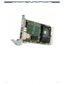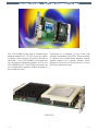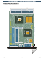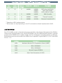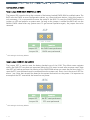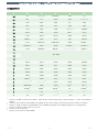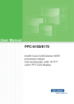
1
User Guide
CCG-RUMBA • CompactPCI ®
3U CoreTM 2 Duo CPU Board
Document No. 4733 • Edition 16 • 17 June 2011
User Guide CCG-RUMBA • CoreTM 2 Duo 3U CompactPCI® CPU Board
Contents
About this Manual . . . . . . . . . . . . . . . . . . . . . . . . . . . . . . . . . . . . . . . . . . . . . . . . . . . . . . . . . . .
Edition History . . . . . . . . . . . . . . . . . . . . . . . . . . . . . . . . . . . . . . . . . . . . . . . . . . . . . . . . .
Legal Disclaimer - Liability Exclusion . . . . . . . . . . . . . . . . . . . . . . . . . . . . . . . . . . . . . . . . .
Trade Marks . . . . . . . . . . . . . . . . . . . . . . . . . . . . . . . . . . . . . . . . . . . . . . . . . . . . . . . . . .
Related Documents . . . . . . . . . . . . . . . . . . . . . . . . . . . . . . . . . . . . . . . . . . . . . . . . . . . . .
4
4
4
4
5
CCG-RUMBA Features . . . . . . . . . . . . . . . . . . . . . . . . . . . . . . . . . . . . . . . . . . . . . . . . . . . . . . . . 6
Feature Summary . . . . . . . . . . . . . . . . . . . . . . . . . . . . . . . . . . . . . . . . . . . . . . . . . . . . . . 6
Short Description . . . . . . . . . . . . . . . . . . . . . . . . . . . . . . . . . . . . . . . . . . . . . . . . . . . . . . 11
Block Diagram . . . . . . . . . . . . . . . . . . . . . . . . . . . . . . . . . . . . . . . . . . . . . . . . . . . . . . . . 13
Top/Bottom View Component Assembly . . . . . . . . . . . . . . . . . . . . . . . . . . . . . . . . . . . . 14
Rear I/O Transition Module CCT-RIO . . . . . . . . . . . . . . . . . . . . . . . . . . . . . . . . . . . . . . . . 17
Strapping Headers . . . . . . . . . . . . . . . . . . . . . . . . . . . . . . . . . . . . . . . . . . . . . . . . . . . . . 20
Connectors & Sockets . . . . . . . . . . . . . . . . . . . . . . . . . . . . . . . . . . . . . . . . . . . . . . . . . . 20
Front Panel Elements . . . . . . . . . . . . . . . . . . . . . . . . . . . . . . . . . . . . . . . . . . . . . . . . . . . 20
Microprocessor . . . . . . . . . . . . . . . . . . . . . . . . . . . . . . . . . . . . . . . . . . . . . . . . . . . . . . . 21
Thermal Considerations . . . . . . . . . . . . . . . . . . . . . . . . . . . . . . . . . . . . . . . . . . . . . . . . . 21
Main Memory . . . . . . . . . . . . . . . . . . . . . . . . . . . . . . . . . . . . . . . . . . . . . . . . . . . . . . . . 23
LAN Subsystem . . . . . . . . . . . . . . . . . . . . . . . . . . . . . . . . . . . . . . . . . . . . . . . . . . . . . . . 23
Serial ATA Interface (SATA) . . . . . . . . . . . . . . . . . . . . . . . . . . . . . . . . . . . . . . . . . . . . . . 24
Enhanced IDE Interface . . . . . . . . . . . . . . . . . . . . . . . . . . . . . . . . . . . . . . . . . . . . . . . . . 24
Graphics Subsystem . . . . . . . . . . . . . . . . . . . . . . . . . . . . . . . . . . . . . . . . . . . . . . . . . . . 24
Real-Time Clock . . . . . . . . . . . . . . . . . . . . . . . . . . . . . . . . . . . . . . . . . . . . . . . . . . . . . . . 25
Universal Serial Bus (USB) . . . . . . . . . . . . . . . . . . . . . . . . . . . . . . . . . . . . . . . . . . . . . . . 26
LPC Super-I/O Interface . . . . . . . . . . . . . . . . . . . . . . . . . . . . . . . . . . . . . . . . . . . . . . . . . 26
SPI Flash . . . . . . . . . . . . . . . . . . . . . . . . . . . . . . . . . . . . . . . . . . . . . . . . . . . . . . . . . . . . 26
Reset . . . . . . . . . . . . . . . . . . . . . . . . . . . . . . . . . . . . . . . . . . . . . . . . . . . . . . . . . . . . . . . 27
Watchdog . . . . . . . . . . . . . . . . . . . . . . . . . . . . . . . . . . . . . . . . . . . . . . . . . . . . . . . . . . . 29
PG (Power Good) LED . . . . . . . . . . . . . . . . . . . . . . . . . . . . . . . . . . . . . . . . . . . . . . . . . . 30
HD (Hard Disk Activity) LED . . . . . . . . . . . . . . . . . . . . . . . . . . . . . . . . . . . . . . . . . . . . . . 30
GP (General Purpose) LED . . . . . . . . . . . . . . . . . . . . . . . . . . . . . . . . . . . . . . . . . . . . . . . 30
Hot Swap Detection . . . . . . . . . . . . . . . . . . . . . . . . . . . . . . . . . . . . . . . . . . . . . . . . . . . 31
Power Supply Status (DEG#, FAL#) . . . . . . . . . . . . . . . . . . . . . . . . . . . . . . . . . . . . . . . . 31
PXI Trigger Signals . . . . . . . . . . . . . . . . . . . . . . . . . . . . . . . . . . . . . . . . . . . . . . . . . . . . . 31
Rear I/O Options . . . . . . . . . . . . . . . . . . . . . . . . . . . . . . . . . . . . . . . . . . . . . . . . . . . . . . 32
Installing and Replacing Components . . . . . . . . . . . . . . . . . . . . . . . . . . . . . . . . . . . . . . . . . . . .
Before You Begin . . . . . . . . . . . . . . . . . . . . . . . . . . . . . . . . . . . . . . . . . . . . . . . . . . . . . .
Installing the Board . . . . . . . . . . . . . . . . . . . . . . . . . . . . . . . . . . . . . . . . . . . . . . . . . . . .
Removing the Board . . . . . . . . . . . . . . . . . . . . . . . . . . . . . . . . . . . . . . . . . . . . . . . . . . .
EMC Recommendations . . . . . . . . . . . . . . . . . . . . . . . . . . . . . . . . . . . . . . . . . . . . . . . . .
Installing or Replacing the Memory Modules . . . . . . . . . . . . . . . . . . . . . . . . . . . . . . . . .
Replacement of the Battery . . . . . . . . . . . . . . . . . . . . . . . . . . . . . . . . . . . . . . . . . . . . . .
33
33
34
35
36
37
37
Technical Reference . . . . . . . . . . . . . . . . . . . . . . . . . . . . . . . . . . . . . . . . . . . . . . . . . . . . . . . . .
Local PCI Devices . . . . . . . . . . . . . . . . . . . . . . . . . . . . . . . . . . . . . . . . . . . . . . . . . . . . . .
Local SMB Devices . . . . . . . . . . . . . . . . . . . . . . . . . . . . . . . . . . . . . . . . . . . . . . . . . . . . .
Hardware Monitor LM87 . . . . . . . . . . . . . . . . . . . . . . . . . . . . . . . . . . . . . . . . . . . . . . . .
GPIO Usage . . . . . . . . . . . . . . . . . . . . . . . . . . . . . . . . . . . . . . . . . . . . . . . . . . . . . . . . . .
GPIO Usage ICH8 . . . . . . . . . . . . . . . . . . . . . . . . . . . . . . . . . . . . . . . . . . . . . . . .
GPIO Usage SIO . . . . . . . . . . . . . . . . . . . . . . . . . . . . . . . . . . . . . . . . . . . . . . . . .
38
38
39
40
41
41
43
© EKF
-2-
ekf.com
User Guide CCG-RUMBA • CoreTM 2 Duo 3U CompactPCI® CPU Board
Configuration Jumpers . . . . . . . . . . . . . . . . . . . . . . . . . . . . . . . . . . . . . . . . . . . . . . . . .
Reset Jumper BIOS CMOS RAM Values (JGP) . . . . . . . . . . . . . . . . . . . . . . . . . . . .
Reset Jumper ICH8 RTC Core (JRTC) . . . . . . . . . . . . . . . . . . . . . . . . . . . . . . . . . . .
Connectors . . . . . . . . . . . . . . . . . . . . . . . . . . . . . . . . . . . . . . . . . . . . . . . . . . . . . . . . . .
Front Panel Connectors . . . . . . . . . . . . . . . . . . . . . . . . . . . . . . . . . . . . . . . . . . . .
Video Monitor Connector DVI-I . . . . . . . . . . . . . . . . . . . . . . . . . . . . . . . .
Video Monitor Connector VGA . . . . . . . . . . . . . . . . . . . . . . . . . . . . . . . . .
USB Connectors . . . . . . . . . . . . . . . . . . . . . . . . . . . . . . . . . . . . . . . . . . . .
Ethernet Connectors . . . . . . . . . . . . . . . . . . . . . . . . . . . . . . . . . . . . . . . .
Internal Connectors . . . . . . . . . . . . . . . . . . . . . . . . . . . . . . . . . . . . . . . . . . . . . .
Expansion Interface Header PEXP . . . . . . . . . . . . . . . . . . . . . . . . . . . . . . .
ATA/IDE Header PIDE . . . . . . . . . . . . . . . . . . . . . . . . . . . . . . . . . . . . . . . .
PCI Express Expansion Header PPCIE . . . . . . . . . . . . . . . . . . . . . . . . . . . . .
SDVO Expansion Header PSDVO . . . . . . . . . . . . . . . . . . . . . . . . . . . . . . . .
System Reset Header JRST . . . . . . . . . . . . . . . . . . . . . . . . . . . . . . . . . . . .
PLD Programming Header ISPCON . . . . . . . . . . . . . . . . . . . . . . . . . . . . . .
Processor Debug Header PITP . . . . . . . . . . . . . . . . . . . . . . . . . . . . . . . . . .
CompactPCI J1 . . . . . . . . . . . . . . . . . . . . . . . . . . . . . . . . . . . . . . . . . . . . .
CompactPCI J2 . . . . . . . . . . . . . . . . . . . . . . . . . . . . . . . . . . . . . . . . . . . . .
Literature . . . . . . . . . . . . . . . . . . . . . . . . . . . . . . . . . . . . . . . . . . . . . . . . . . . . . . . . . . .
44
44
44
45
45
46
47
47
48
49
58
59
60
61
61
62
62
63
64
66
Appendix . . . . . . . . . . . . . . . . . . . . . . . . . . . . . . . . . . . . . . . . . . . . . . . . . . . . . . . . . . . . . . . . .
Mechanical Drawings . . . . . . . . . . . . . . . . . . . . . . . . . . . . . . . . . . . . . . . . . . . . . . . . . .
Mass Storage Considerations . . . . . . . . . . . . . . . . . . . . . . . . . . . . . . . . . . . . . . . . . . . . .
Coating . . . . . . . . . . . . . . . . . . . . . . . . . . . . . . . . . . . . . . . . . . . . . . . . . . . . . . . . . . . . .
Sample Applications . . . . . . . . . . . . . . . . . . . . . . . . . . . . . . . . . . . . . . . . . . . . . . . . . . .
67
67
68
73
75
© EKF
-3-
ekf.com
User Guide CCG-RUMBA • CoreTM 2 Duo 3U CompactPCI® CPU Board
About this Manual
This manual describes the technical aspects of the CCG-RUMBA, required for installation and system
integration. It is intended for the experienced user only.
Edition History
Ed.
Contents/Changes
Author
Date
gn
2007-08-16
jj
2008-02-07
1
User Manual CCG-RUMBA, english, initial edition (Text #4733, File: ccg_uge.wpd)
2
Added Jumbo Frame support information to table 'Feature Summary'
3
Added Typical Power Requirements andPerformance Ratings to table 'Feature
Summary'
gn
2008-03-25
4
Split section 'Reset/Watchdog' in two separate sections. Added clarification of
function of front panel handle in section 'Reset'
gn
2008-10-21
5
Added images C10-CFA & C17-CFA, C13-RD
jj
25 November 2008
6
Added images section 'Internal Connectors' (several side boards)
jj
5 January 2009
7
Added figure to chapter 'Thermal Considerations'.
gn
2009-01-22
8
Corrected typo within CompactPCI J2 connection table.
gn
2009-03-17
9
Added photos of coated PCB, added photos of CCO-CONCERT, added photos C29RIO, established table with web-links to other documents and downloads
jj
11 September 2009
10
Added photos of CCT-99-RIO, removed photos of C29-RIO
jj
6 November 2009
11
Added photos CCG-RUMBA CCK-MARIMBA DE4-FOX/DX1-LYNX exploded view
jj
18 November 2009
12
Added description of unlocked front panel handle signalling
gn
2011-04-14
13
BIOS usage of GP LED - document link added
Power button illustration added
jj
18 May 2011
14
Blinking yellow GP LED described more clearly, highlighted 'S5 if handle not closed'
jj
31 May 2011
15
Typos corrected
jj
6 June 2011
16
Highlighted BIOS GP LED Usage Link
gn
2011-06-17
Legal Disclaimer - Liability Exclusion
This manual has been edited as carefully as possible. We apologize for any potential mistake. Information
provided herein is designated exclusively to the proficient user (system integrator, engineer). EKF can accept no
responsibility for any damage caused by the use of this manual.
Trade Marks
Some terms used herein are property of their respective owners, e.g.
<
<
<
<
Pentium, Pentium M, Celeron M, Core 2 Duo, Merom, Crestline GME965, Santa Rosa Platform, Nineveh,
Matanzas CRB, iAMT: ® Intel
CompactPCI : ® PICMG
Windows 2000, Windows XP, Windows Vista: ® Microsoft
EKF, ekf system: ® EKF
EKF does not claim this list to be complete.
© EKF
-4-
ekf.com
User Guide CCG-RUMBA • CoreTM 2 Duo 3U CompactPCI® CPU Board
Related Documents
Links to PDF Documents
CCG-RUMBA User Guide
This Document, Latest Edition
www.ekf.com/c/ccpu/ccg/ccg_uge.pdf
CCG-RUMBA Ordering Information (Excerpt)
Ordering Numbers at the End of Document
www.ekf.com/c/ccpu/ccg/ccg_pie.pdf
C10-C13-C17 CompactFlash™ Adapter Modules
www.ekf.com/c/ccpu/c13/c13_pie.pdf
C20-SATA Dual Drive Storage Module
www.ekf.com/c/ccpu/c20/c20_tie.pdf
C30-PATA 1.8-Inch IDE Drive Storage Module
www.ekf.com/c/ccpu/c30/c30_pie.pdf
C23-SATA Mezzanine Side Board
SATA, COM, AC'97 Audio
www.ekf.com/c/ccpu/c23/c23_tie.pdf
CCE-PUNK Mezzanine Side Board
COM, USB, FireWire
www.ekf.com/c/ccpu/cce/cce_tie.pdf
CCH-MARIACHI Mezzanine Side Board
HD Audio, DVI Video, COM, USB
www.ekf.com/c/ccpu/cch/cch_tie.pdf
CCI-RAP Mezzanine Side Board
Dual PCIe Mini Card, DVI Video
www.ekf.com/c/ccpu/cci/cci_tie.pdf
CCJ-RHYTHM Mezzanine Side Board
CompactPCI Express System Slot
www.ekf.com/c/ccpu/ccj/ccj_tie.pdf
CCK-MARIMBA Mezzanine Side Board
XMC/PMC Module Carrier
www.ekf.com/c/ccpu/cck/cck_tie.pdf
CCL-CAPELLA Mezzanine Side Board
Quad Gigabit Ethernet
www.ekf.com/c/ccpu/ccl/ccl_tie.pdf
CCO-CONCERT Mezzanine Side Board
HD Audio, DVI Video, SATA
www.ekf.com/c/ccpu/cco/cco_tie.pdf
CCT-RIO Rear I/O Transition Module
www.ekf.com/c/ccpu/cct/cct_tie.pdf
This table may be not complete. Please visit the CCG-RUMBA home for current information.
Links to BIOS and Driver Downloads
CCG-RUMBA Home (Drivers)
www.ekf.com/c/ccpu/ccg/ccg_e.html
CCG-RUMBA BIOS and Firmware
www.ekf.com/c/ccpu/ccg/firmware/
BIOS Update Notification Subscription
www.ekf.com/new/sub_e.html
© EKF
-5-
ekf.com
User Guide CCG-RUMBA • CoreTM 2 Duo 3U CompactPCI® CPU Board
CCG-RUMBA Features
Feature Summary
Feature Summary CCG-RUMBA
Form Factor
Single size CompactPCI style Eurocard (160x100mm2), front panel width 4HP
(20.3mm)
Processor
Designed for Intel® Core™ 2 Duo second generation dual core mobile processors
(codename Merom), dynamic FSB switching, 800/667/533MHz FSB, maximum
junction temperature 100°C, Intel® Core Multiprocessing (CMP), Intel® Virtualization
Technology (VT), Intel® 64 Architecture
<
<
<
<
Chipset
Intel® GME965 (Codename Crestline) chipset comprised of:
<
<
Memory (RAM)
<
<
<
© EKF
GME965 Graphics/Memory Controller Hub (GMCH) with Intel® Graphics
Media Accelerator (GMA), generation 4 graphics engine, DirectX 10 and
OpenGL 2.0 support, 1.5 x 945GM graphics performance, iAMT manageability
engine
ICH8M-E Enhanced I/O Controller Hub, integrated GbE MAC, dual USB EHCI
controllers (no shared bandwidth), 3 x SATA 3Gbps, MST & RAID, iAMT,
unified SPI Flash support
Dual 200-pin SO-DIMM socket, DDR2 667 SDRAM (PC5300), 4GB (2 x 2GB)
maximum, single or dual channel mode operation, configurations:
<
<
Non Volatile
Memory (NVM)
CCG-1-RUMBA: 1.06GHz U7500 Intel® Core™ 2 Duo ULV, 533MHz FSB, 2MB
L2 cache, TDP ~10W (low power applications)
CCG-2-RUMBA: 1.2GHz U7600 Intel® Core™ 2 Duo ULV, 533MHz FSB, 2MB
L2 cache, TDP ~10W (low power applications)
CCG-4-RUMBA: 1.6GHz L7500 Intel® Core™ 2 Duo LV, 800MHz FSB, 4MB L2
cache, TDP 17W (general purpose applications)
CCG-8-RUMBA: 2.2GHz T7500 Intel® Core™ 2 Duo, 800MHz FSB, 4MB L2
cache, TDP 35W (performance applications)
256Mb, 512Mb, 1Gb, 2Gb technologies for x8 and x16 devices
Dual channel symmetric – memory addresses interleaved for increased
performance
Intel® Flex Memory Technology (dual channel interleaved mode with unequal
memory population) - memory module sizes maybe unequal in both the
channels
Dual channel asymmetric – memory module sizes may differ, including no
memory in the second channel (single-channel)
Channel 0 must be populated first
Intel® Turbo Memory card (codename Robson) on CCI-RAP mezzanine side board
optionally available
<
PCI Express Mini Card 1G Byte Flash
<
Microsoft® ReadyDrive and ReadyBoost (Windows® Vista)
<
Intel® Turbo Memory driver
-6-
ekf.com
User Guide CCG-RUMBA • CoreTM 2 Duo 3U CompactPCI® CPU Board
Feature Summary CCG-RUMBA
Video
<
<
<
<
<
USB
<
<
<
<
<
<
Ethernet
<
<
<
<
PATA (IDE)
<
<
<
SATA
<
<
<
<
PCI Express
© EKF
Both analog monitor and digital flat-panel display support by DVI-I connector
(front panel), up to 2048x1536 pixel 16M colours @75Hz refresh rate
(analog), up to 1920 x 1200 pixel 16M colours @60Hz (digital), incorporates
PanelLink Digital technology (Silicon Image)
Dual screen capable up to 2 x 1920 x 1200 pixel (one display attached to the
front panel, the other to the back panel, or both to the front panel by means
of a DVI-I to DVI-D/VGA splitter cable, or secondary DVI-D connector on
mezzanine side board)
Front panel option: D-Sub (female HD15) VGA connector available, replaces
DVI-I connector
Rear I/O option: Analog video output configurable (BIOS) across J2/P2 CCT-RIO
rear I/O transition module
Mezzanine option: Secondary DVI-D connector at mezzanine card front panel
allows for dual digital flat panel operation, suitable mezzanine modules e.g.
CCH-MARIACHI, CCI-RAP or CCJ-RHYTHM
All ports over-current protected, data transfer rate of up to 480Mbps,
conforming to USB2.0
2 x USB type A connector (front panel)
3 x USB ports J2/P2 Rear I/O option (CCT-RIO rear I/O transition module)
up to 2 x USB ports expansion interface option (in use by several mezzanine
side boards)
USB Flash drive module C15-DON option (USB stick on-board module)
Dual EHCI / five UHCI controllers provided by ICH8M-E
Two 10/100/1000Mbps Gigabit Ethernet controllers, accessible via RJ45 jacks
from the front panel
ETH1 equipped with Intel® 82566 PHY (codename Nineveh), serves also as
AMT out of band communication path (MAC provided by ICH8M-E), no
Jumbo Frame support with 82566MM
ETH2 equipped with Intel® 82573 GbE controller connected to local PCIe
lane, Jumbo Frame support with 82573L up to 9kB
Option ETH1 Gigabit Ethernet configurable (BIOS setup) across J2/P2 with
attached CCT-RIO rear I/O transition module
Ultra ATA/100 connector, handover to CCH-MARIACHI/CCJ-RHYTHM
mezzanine expansion board with optional on-board 2.5-inch hard disk drive or
external device
CompactFlash socket C10-1D-CFA supplied for a CFA ATA memory card or
Microdrive®
Option 1.8-inch on board Flash disk (SSD) module C10-2D-CFA, replaces
CompactFlash facility
Triple-channel Serial ATA 3Gbps available for J2/P2 rear I/O option
Suitable rear I/O transition module CCT-RIO (2 x system internal SATA, 1 x
eSATA for attachment of external devices)
Intel® Matrix Storage Technology MST (Raid 1, 0, Matrix Raid)
Additional PCIe to SATA controller on mezzanine side boards CCI-RAP, CCKMARIMBA
4-Lane PCIe (1 Link) connector for CCJ-RHYTHM and other mezzanine expansion cards
(side boards)
-7-
ekf.com
User Guide CCG-RUMBA • CoreTM 2 Duo 3U CompactPCI® CPU Board
Feature Summary CCG-RUMBA
Mezzanine
Side Board
I/O
<
<
<
<
<
LPC/USB/Audio (Super-I/O, USB and Azalia HD Audio) expansion interface
connector
ATA/IDE expansion connector
PCI Express 4-lane (configurable as 1 link x 4) high speed expansion connector
SDVO secondary digital graphics port high speed expansion connector
Suitable mezzanine companion side boards available:
<
<
<
<
<
<
<
<
<
<
<
<
<
J2/P2 Rear I/O
<
<
<
<
<
<
<
C10-CFA: CompactFlash adapter module (CF Card internally)
C13-RD: CompactFlash adapter module (CF Card front panel slot,
resulting in a 6HP assembly)
C15-DON: On-board USB stick module (USB Flash disk)
C17-CFA: Bottom Mount CF Card Adapter
C23-SATA: PCIe to SATA controller, USB SSD, COM ports
C30-PATA: 1.8-inch HDD/SSD module
CCE-PUNK: Front panel 2 x COM, 2 x USB, 2 x 1394a FireWire, on
board hard disk
CCH-MARIACHI: Front panel options secondary DVI-D, COM, USB,
audio in (analog), audio out (analog), digital audio. Option on board
PATA hard disk drive 2.5-inch, option TPM 1.2
CCI-RAP: Front panel options secondary DVI-D, Wireless (Antenna),
IEEE 1394 (FireWire), COM. Two PCI Express Mini Card sockets (WLAN,
GSM, Wimax, Intel® Turbo Memory), on board socket for USB Flash
disk. Option on board mezzanine storage module C20 provides up to
2 SATA hard disk drives 2.5-inch (RAID capable), option TPM 1.2
CCJ-RHYTHM: Front panel options DVI-D, COM, USB, IEEE 1394
(FireWire). CompactPCI Express system slot controller function by on
board 6-port 24-lane PCIe switch. Option on board PATA hard disk
drive 2.5-inch, option TPM 1.2
CCK-MARIMBA: PMC/XMC module carrier. Option on board
mezzanine storage module C20-SATA
CCL-CAPELLA: 4 x Gigabit Ethernet, IEEE 1394 (FireWire), option on
board mezzanine storage module C20-SATA
CCO-CONCERT: HD Audio, 2-4 x RS-232, secondary DVI-I (option),
several on-board SATA drive options 1.8-inch and 2.5-inch (up to 2
drives), USB Flash Disk option, option TPM 1.2
3 x Serial ATA (SATA), 2 x system internal SATA connectors, 1 x external eSATA
connector
1 x Gbit Ethernet (switched by BIOS between front panel I/O and rear I/O)
3 x USB
VGA Analog Video (switched by BIOS between front panel I/O and rear I/O)
Keyboard, Mouse
COM port (TTL Level)
Suitable rear I/O transition module CCT-RIO available
CompactPCI®
ICH8M-E integrated 32-bit PCI bridge, 133MBps CPCI master, additional PCI arbiter in
PLD for fully figured 8-slot CompactPCI backplane
CompactPCI®
Express
<
<
<
© EKF
CCG-RUMBA works also as CompactPCI Express System Board (system slot
controller) by optionally available mezzanine expansion card (side board) CCJRHYTHM
CPCIe 4-Link configuration (4-lanes each), for up to 4 CPCIe peripheral slots
type 1 and/or type 2 on a passive CPCIe backplane
Suitable also for hybrid CPCI/CPCIe systems/backplanes (e.g. Schroff)
-8-
ekf.com
User Guide CCG-RUMBA • CoreTM 2 Duo 3U CompactPCI® CPU Board
Feature Summary CCG-RUMBA
Platform
Management
<
<
<
AMT 2.0 Intel® Active Management Technology (iAMT)
ARM core based Manageability Engine (ME) in the GMCH
Independent manageability firmware, stored in SPI Flash
Secure
Computing
<
<
Option Trusted Platform Module TPM 1.2 according to Trusted Computing
Group specifications, available on several mezzanine boards such as
CCH/CCI/CCJ
Crypto engine silicon brands Infineon or Atmel at users choice
BIOS
<
<
<
Phoenix BIOS with EKF enhancements for embedded systems
SPI Flash memory 2 x 16/32/64 Mb
Updates available from website ekf.com
Drivers
(All Major OS)
<
<
<
<
Intel® graphics driver
Intel® networking driver
Intel® Matrix Storage Manager software
Intel® Turbo Memory driver
Thermal
Conditions
Environmental
Conditions
<
<
<
<
<
<
Operating temperature: 0°C ... +70°C (CPU dependent)
Storage temperature: -40°C ... +85°C, max. gradient 5°C/min
Humidity 5% ... 95% RH non condensing
Altitude -300m ... +3000m
Shock 15g 0.33ms, 6g 6ms
Vibration 1g 5-2000Hz
EC Regulations
<
<
EN55022, EN55024, EN60950-1 (UL60950-1/IEC60950-1)
2002/95/EC (RoHS)
MTBF
tbd
Typical Power
Requirements
+3.3V +0.17V/-0.1V
Board
MaxPower
LFM/HFM 1)
WinXP Idle
LFM/HFM 1)
MaxPower
LFM/HFM 1)
WinXP Idle
LFM/HFM 1)
CCG-1-RUMBA
4.9/4.9A 2)
1.7/1.7A 2)
2.1/2.6A
1.0/1.1A
CCG-4-RUMBA
5.3/5.3A 2)
1.8/1.8A 2)
3.1/4.0A
1.2/1.5A
CCG-8-RUMBA
5.3/5.3A 2)
1.8/1.8A 2)
3.1/7.8A
1.4/2.2A
1)
Intel®
SpeedStep®
Frequency
Modes
LFM: Low
Frequency Mode,
HFM: High
Frequency Mode
2)
+5V +0.25V/-0.15V
Add 0.8A per Ethernet Port @1Gbps or 0.2A per Ethernet Port @100Mbps.
Performance
Rating
Measured with
PCMark2005
under Windows
XP, 2 x 1GB
DDR2 667
Board
Processor
CPU/MEM Score
CCG-1-RUMBA
U7500
2330
CCG-4-RUMBA
L7500
3090
CCG-8-RUMBA
T7500
3760
Table items are subject to technical changes
© EKF
-9-
ekf.com
User Guide CCG-RUMBA • CoreTM 2 Duo 3U CompactPCI® CPU Board
© EKF
-10-
ekf.com
User Guide CCG-RUMBA • CoreTM 2 Duo 3U CompactPCI® CPU Board
Short Description
The CCG-RUMBA is a versatile 4HP/3U (single
size Eurocard) CompactPCI® CPU board,
equipped with an Intel® Core™ 2 Duo
processor at 2.2GHz clock, and up to 4GB dual
channel capable DDR2 RAM. Three Serial ATA
channels are available for rear I/O. The
CCG-RUMBA has been designed especially for
systems which require very high performance at
moderate power consumption.
The CCG-RUMBA is provided with a high
performance mobile chipset (Intel® GME965)
which operates at up to 800MHz FSB and up to
667MHz DDR2 memory clock for optimum
system throughput. An on-board CF connector
can accommodate either a CompactFlash
memory card or a Microdrive®. As an alternate,
a 1.8-inch Flash disk module is available as onboard mass-storage device (option).
The chipset is based on PCI Express technology
and has a powerful dual-screen integrated
graphics accelerator. Two Gigabit Ethernet
controllers are provided for high speed
connectivity. As an option, a mezzanine card is
available that allows to use the CCG-RUMBA in
addition as CompactPCI® Express system slot
controller (especially suited for hybrid dual
backplane systems).
Local expansion interface connectors can be
optionally used to directly attach a mezzanine
companion sideboard, either for audio- and
legacy support, or equipped with PCI Express
based I/O circuitry. Mezzanine cards can carry in
addition a 2.5-inch hard disk drive. Also as an
option, a suitable rear I/O transition module is
available to the CCG-RUMBA, which e.g.
provides the Serial ATA connectors.
Benefits of the CCG-RUMBA
<
<
<
<
<
<
<
<
<
<
<
<
<
<
<
<
© EKF
CompactPCI System Slot Controller with or w/o Rear I/O
CompactPCI Express System Board Option (Mezzanine Expansion Card)
Hybrid Systems Option (Dual Backplane CompactPCI & CompactPCI Express)
Intel® Core™ 2 Duo Mobile Processor 2.2GHz (FSB 800MHz)
PCI Express Mobile Chipset Intel® GME965
2 x 2GB DDR2 Memory (Dual Channel Mode Capable)
Dual-Screen Graphics Controller
Dual Gigabit Ethernet Controllers
Triple SATA 3Gbps, Intel® Matrix Raid Storage Technology
Seven USB 2.0 channels
On-Board CompactFlash or on-Board 1.8-Inch Flash Disk
Mezzanine Expansion Boards Available with or w/o PCIe
TPM 1.2 Option (on Mezzanine Expansion Board)
Rear I/O Transition Module Option
Intel® AMT 2.0 Platform Management
RoHS compliant
-11-
ekf.com
User Guide CCG-RUMBA • CoreTM 2 Duo 3U CompactPCI® CPU Board
CCG-RUMBA w C10-CFA
The CCG-RUMBA comes with a CompactFlash
adapter module (C10-1D-CFA), which is suitable
to hold a silicon memory CF card or Microdrive
hard disk. If the CCG-RUMBA is accompanied
by a mezzanine expansion module such as the
CCH-MARIACHI or CCJ-RHYTHM, the position of
the CompactFlash adapter module changes to
the mezzanine card.
Optionally an on-board 1.8-inch Flash disk
module is available (C30-PATA). When ordered,
it replaces the CompactFlash adapter module
(please request for a special solution which
allows to use both the CF slot and the 1.8-inch
SSD drive simultaneously).
C30-PATA
© EKF
-12-
ekf.com
User Guide CCG-RUMBA • CoreTM 2 Duo 3U CompactPCI® CPU Board
Block Diagram
Core™2
Duo
Core™2 Duo T7500
2.2GHz FSB800 4MB L2
LV Core™2 Duo L7500
1.6GHz FSB800 4MB L2
Simplified Block Diagram
CCG-RUMBA
2.2GHz
ULV Core™2 Duo U7500
1.06GHz FSB533 2MB L2
533/667/800
Video
Panel
Link
SDVO1
VGA
GME965
RGB
GMCH
SDVO2
Crestline
iAMT
ME
DVI2
VGA
Opt. Mezz. Exp.
CCH-MARIACHI
CCJ-RHYTHM
top/
bottom
DMI x 4
SDVO2
D-SUB
DDR2 533/667
2GB/4GB
Dual Channel
C10-CFA
CompactFlash
ATA
IDE I/F
DVI1
SO-DIMM 200
SO-DIMM 200
MEROM FSB
IDE
Opt. Mezzanine
Expansion Board
CCH-MARIACHI
CCJ-RHYTHM
USB
VGA
ICH8M-E
SPI
USB
KB/MS
SIO
87
61
LPC
HD Audio
PCI
82566
MM
USB
COM
GPIO
iAMT Gb
Ethernet
Front Panel I/O
GbE
2
Gb ETH
J2
BIOS & FW
2 x 16/32Mb
82
573
SPI
FlashSPI
Flash
Gigabit
Ethernet
Glue Logic
PCI Arbiter
4 x PCI
isp
MACH
x 4 PCIe
PCIe
Expansion I/F
top/
bottom
7 x PCI
32bit/33MHz
CompactPCI
GbE
1
PCIe
iAMT
Opt. Rear I/O
CCT-RIO
SATA II
RAID
Rear I/O
Kumeran
GLCI
J1
Opt. Mezz.
Exp. Board
CCH-MARIACHI
CCJ-RHYTHM
© EKF
-13-
ekf.com
© EKF
-14-
GbE2
GbE1
AMT
USB2
USB1
VGA
DVI
-I
82
573
1
©EKF
1
PEXPT/B
1
PSDVO
CCG-RUMBA
GMCH
GME965
SODIMM1
SODIMM2
PIDET/B
1
ekf.com
ICH8M-E
CPU
Core™ 2 Duo
PPCIE
User Guide CCG-RUMBA • CoreTM 2 Duo 3U CompactPCI® CPU Board
Top/Bottom View Component Assembly
ekf.com
User Guide CCG-RUMBA • CoreTM 2 Duo 3U CompactPCI® CPU Board
© EKF
-15-
ekf.com
User Guide CCG-RUMBA • CoreTM 2 Duo 3U CompactPCI® CPU Board
Bottom View CCG-RUMBA
© EKF
-16-
ekf.com
User Guide CCG-RUMBA • CoreTM 2 Duo 3U CompactPCI® CPU Board
Rear I/O Transition Module CCT-RIO
Available as a rear I/O expansion board to the
CCG-RUMBA CPU card, the CCT-RIO is provided
with several I/O port connectors, to be used
either in addition to the CCG-RUMBA front
panel connectors or alternatively. Being mainly
a passive rear I/O transition module, groups of
signals from the CCG-RUMBA CPU board are
passed across the CompactPCI J2/P2 connector
to the CCT-RIO. Some of the data lines are
available locally on the CCT board for system
internal wiring only, while other connectors
such as VGA-Video and Gigabit Ethernet are
mounted into the back panel for external use.
USB and SATA (eSATA) channels are provided
both on-board and externally.
Typically the CCT-RIO ist equipped with a 4-HP
rear panel (20.3mm width). As a custom
specific option, an 8-HP panel is available with
additional connectors.
Utilization of the CCT-RIO transition module
adds a level of I/O functionality that is not
available with the CCG-RUMBA CPU board
alone. Further on, swapping the CPU card is
simplified by means of rear I/O, which is
important for efficient system maintenance
(MTTR). Be sure to have ordered a CCG-RUMBA
rear I/O capable version and also the CPCI
backplane suitable for rear I/O in order to use
the CCT-RIO transition module.
CCT-RIO (Shown with on-Board USB Stick)
© EKF
-17-
ekf.com
User Guide CCG-RUMBA • CoreTM 2 Duo 3U CompactPCI® CPU Board
VGA
Block Diagram
CCT-RIO
Video
ADM
211
COM
RS-232E
Ethernet
USB
ETH
LM
3526
USB
SATA
USB
Option 8HP
Rear Panel
I/O
CCD-CALYPSO
J2 Rear I/O
KB
MS
P-POW
SATA
KB/MS
4HP
Rear Panel
I/O
J2
COM
TTL
J-COM
COM
Rear I/O
GPIO
+5V
CCG-RUMBA with CCT-RIO
© EKF
-18-
ekf.com
User Guide CCG-RUMBA • CoreTM 2 Duo 3U CompactPCI® CPU Board
CCT-99-RIO Custom Specific for Internal I/O Usage
CCT-99-RIO Custom Specific for Internal I/O Usage
© EKF
-19-
ekf.com
User Guide CCG-RUMBA • CoreTM 2 Duo 3U CompactPCI® CPU Board
Strapping Headers
ISPCON
PLD Programming Connector, not stuffed
JGP
Jumper to Reset BIOS CMOS RAM Values
JRST
Jumper to Reset Board
JRTC
Jumper to Reset RTC Core of ICH8, not stuffed
Connectors & Sockets
J1/J2
CompactPCI Bus 32-bit, 33MHz, PXI, Rear I/O
PEXPT
PEXPB
Expansion Interface Connector (LPC Interface (2nd Super-I/O, 2nd
FWH), USB Interfaces, HD Audio Interface, SMBus), available either
from top (T) or bottom (B) of the board
PIDET
PIDEB
Ultra ATA/100 IDE Port (Interface to CompactFlash ATA Socket on
C10-CFA), available either from top (T) or bottom (B) of the board
PITP
CPU Debug Port
PPCIE
PCI Express Expansion Interface Connector
SODIMM1
SODIMM2
200-pin DDR2 Memory Module SDRAM PC2-4200/5300
(DDR533/667) Sockets
Front Panel Elements
© EKF
Ethernet
(GbE1/2)
Dual 1000Base-TX/100Base-TX/10Base-T, RJ-45 Receptacles with
integrated indicator LEDs
Graphics
(DVI-I)
DVI-I Integrated (digital & analog) Receptacle, suitable for DVI digital
flat panel displays and/or analog monitors
USB1/2
Universal Serial Bus 2.0 self powered root hub, type A receptacle
GP
General Purpose LED
HD
LED indicating any activity on IDE or SATA ports
PG
LED indicating Power Good/Board Healthy
-20-
ekf.com
User Guide CCG-RUMBA • CoreTM 2 Duo 3U CompactPCI® CPU Board
Microprocessor
The CCG-RUMBA is designed for use with CoreTM2 Duo processors manufactured in 65nm technology.
These includes also the Ultra Low-Voltage (ULV) and the Low-Voltage (LV) CoreTM2 Duo processors as
listed below. The processors are housed in a Micro FC-BGA package for direct soldering to the PCB,
i.e. the CPU chip cannot be removed or changed by the user.
The processors supported by the CCG-RUMBA are running at FSB clock speeds of 533MHz, 667MHz
and 800MHz. The internal CoreTM2 Duo processor speed is achieved by multiplying the host bus
frequency by a variable value. The multiplier is chosen by currently required performance and the
actual core temperature. To further lowering the power dissipation, the processor is able to halve its
FSB clock speed dynamically. This technology is called Enhanced Intel SpeedStep®.
Power is applied across the CompactPCI connectors J1 (3.3V, 5V). The processor core voltage is
generated by a switched voltage regulator, sourced from the 5V plane. The processor signals its
required core voltage by 7 dedicated pins according to Intels IMVP-6 voltage regulator specification.
65nm Processors Supported
1)
Processor
Number
of Cores
Speed
min/max
[GHz]
Host
Bus
[MHz]
L2
Cache
[MB]
TDP
[W]
Die Temp
[°C]
CPU ID
Stepping
sSpec
ULV Core 2 Duo
U7500
2
0.80/1.06
533
2
10
0-100
06FDh
M-0
SLV3X
ULV Core 2 Duo
U7600 1)
2
0.80/1.20
533
2
10
0-100
06FDh
M-0
SLV3W
LV Core 2 Duo
L7500
2
0.80/1.60
800
4
17
0-100
06FAh
E-1
SLA3R
SV Core 2 Duo
T7500
2
0.80/2.20
800
4
35
0-100
06FAh
E-1
SLA3N
Following the Intel Embedded Roadmap, this processor is not recommended for long time
availability.
Thermal Considerations
In order to avoid malfunctioning of the CCG-RUMBA, take care of appropriate cooling of the
processor, GMCH and system, e.g. by a cooling fan suitable to the maximum power consumption of
the CPU chip actually in use. Please note, that the processors die temperature is steadily measured by
a special controller (LM87), attached to the onboard SMBus® (System Management Bus). A second
temperature sensor internal to the LM87 allows for acquisition of the boards surface temperature.
Beside this the LM87 also monitors most of the supply voltages. A suitable software to display both,
the temperatures as well as the supply voltages, is MBM (Motherboard Monitor), which can be
downloaded from the web. After installation, both temperatures and voltages can be observed
permanently from the Windows taskbar.
© EKF
-21-
ekf.com
User Guide CCG-RUMBA • CoreTM 2 Duo 3U CompactPCI® CPU Board
The CCG-RUMBA is equipped with a passive heatsink. Its height takes into account the 4HP limitation
in mounting space of a CompactPCI board. In addition, a forced vertical airflow through the system
enclosure (e.g. bottom mount fan unit) is strongly recommended (>10m3/h or 300LFM around the
CPU slot). As an exception, the CCG-1-RUMBA (ULV CoreTM2 Duo 1.06GHz) can be operated with
natural convection only. Be sure to thoroughly discuss your actual cooling needs with EKF. Generally,
the faster the CPU speed the higher its power consumption. For higher ambient temperatures,
consider increasing the forced airflow to 500LFM or higher.
The table showing the supported processors above give also the maximum power consumption (TDP
= Thermal Design Power) of a particular processor. Fortunately, the power consumption is by far
lower when executing typical Windows or Linux tasks. The heat dissipation increases when e.g.
rendering software like the Acrobat Distiller is executed.
The CoreTM2 Duo processors support Intel's Enhanced SpeedStep® technology. This enables dynamic
switching between multiple core voltages and frequencies depending on core temperature and
currently required performance. The processors are able to reduce their core speed and core voltage
in multiple steps down to 800MHz. Furthermore they can reduce their FSB clock speed to half the
frequency. This leads to an obvious reduction of power consumption (max. 12W @800MHz) resulting
in less heating. This mode of lowering the processor core temperature is called TM2 (TM=Thermal
Monitor). The following figure shows the performance derating with increasing ambient temperature
caused by dynamic frequency changes.
Performance Derating
2.2GHz/800MHz FSB Core®2 Duo
Processor T7500
Airflow=2m/s [400lfm]
6000
5000
4000
CPU Score
3000
Memory Score
2000
Graphics Score
1000
0
40 45 50 55 60 65 70 75 80
Temp °C
Another way to reduce power consumption is to
modulate the processor clock. This mode (TM1) is
achieved by actuating the 'Stop Clock' input of the CPU. A
throttling of 50% e.g. means a duty cycle of 50% on the
stop clock input. However, while saving considerable
power consumption, the data throughput of the
processor is also reduced. The processor works at full
speed until the core temperature reaches a critical value.
Then the processor is throttled by 50%. As soon as the
high temperature situation disappears the throttling will
be disabled and the processors runs at full speed again.
A similar feature is embedded within the Graphics and
Memory Controller (GMCH) GME965. An on-die temperature sensor is used to protect the GMCH
from exceeding its maximum junction temperature (TJ,max=110°C) by reducing the memory
bandwidth. These features are controllable by BIOS menu entries. By default the BIOS of the CCGRUMBA enables mode TM2 which is the most efficient.
A very efficient power saving tool is RMClock (for more details please refer to the link below).
http://www.ekf.com/c/ccpu/firmware/rmclock_howto.pdf
© EKF
-22-
ekf.com
User Guide CCG-RUMBA • CoreTM 2 Duo 3U CompactPCI® CPU Board
Main Memory
The CCG-RUMBA is equipped with two sockets for installing 200-pin SO-DIMM modules (module
height = 1.25 inch). Supported are unbuffered DDR2 SO-DIMMs (VCC=1.8V) without ECC featuring
on-die termination (ODT), according the PC2-4200 or PC2-5300 specification. Minimum memory size
is 128MB; maximum memory size is 4GB. Due to the video requirements of the GME965 chipset, a
minimum of 2x512MB of memory is recommended for the operating systems Windows 2000,
Windows XP or Windows Vista (some of the system memory is dedicated to the graphics controller).
The contents of the SPD EEPROM on the SO-DIMMs is used by the BIOS at POST (Power-on Self Test)
to program the memory controller within the chipset.
The GME965 chipset supports symmetric and asymmetric memory organization. The maximum
memory performance can be obtained by using the symmetric mode. When in this mode, the GMCH
accesses the memory sockets in an interleaved way. Since the GME965 supports Intels Flex Memory
Technology, interleaved operation isn't limited to systems using two SO-DIMMs of equal capacity. In
the case of unequal memory population the smaller SO-DIMM dictates the address space of the
interleaved accessible memory region. The remainder of the memory is then accessed in noninterleaved mode.
In asymmetric mode the SO-DIMMs always will be accessed in a non-interleaved manner with the
drawback of less bandwidth. The only meaningful application of asymmetric mode is the special case
when only one SO-DIMM socket is populated (i.e. one socket may be left empty). In order to operate
AMT, SO-DIMM socket 1 should be stuffed then.
LAN Subsystem
The Ethernet LAN subsystem is composed of two Gigabit Ethernet ports: One Intel 82566 physical
layer Transceiver (PHY) using the ICH8 internal MAC and one Intel 82573 Gigabit Ethernet controller.
These devices provide also legacy 10Base-T and 100Base-TX connectivity. The Ethernet ports are fed
to two RJ45 jacks located in the front panel. Each port includes the following features:
C
C
C
C
C
C
One PCI Express lane per Ethernet port (250MB/s)
1000Base-Tx (Gigabit Ethernet), 100Base-TX (Fast Ethernet) and 10Base-T (Classic Ethernet)
capability.
Half- or full-duplex operation.
IEEE 802.3u Auto-Negotiation for the fastest available connection.
Jumperless configuration (complete software-configurable).
Two bicoloured LEDs integrated into the dedicated RJ-45 connector to signal the LAN link, the
LAN connection speed and activity status.
Each device is connected by a single PCI Express lane to the chipset (ICH8). Their MAC addresses
(unique hardware number) are stored in dedicated FLASH/EEPROM components. The Intel Ethernet
software and drivers for the 82566 and 82573 is available from Intel's World Wide Web site for
download.
When managing the board by Intel Active Management Technology (AMT), the dedicated network
port to do so is accessible by the RJ45 connector GbE1.
© EKF
-23-
ekf.com
User Guide CCG-RUMBA • CoreTM 2 Duo 3U CompactPCI® CPU Board
Serial ATA Interface (SATA)
The CCG-RUMBA provides three serial ATA (SATA) ports each capable of transferring 3Gbps
(300MByte/s). Integrated within the ICH8 the SATA controller features different modes to support also
legacy operating systems. The SATA channels are routed to the CompactPCI J2 connector, thus they
are accessible via the rear I/O transition module CCT-RIO.
A LED named HD located in the front panel, signals disk activity status of the SATA and IDE devices.
Available for download from Intel's web site are drivers for popular operating systems, e.g. Windows®
2000, Windows® XP, Windows® Vista and Linux.
Enhanced IDE Interface
The EIDE interface handles the exchange of information between the processor and peripheral devices
like hard disks, ATA CompactFlash cards and CD-ROM drives. The interface supports:
C
C
Up to two ATA devices
PIO Mode 3/4, Ultra ATA/33, Ultra ATA/66, Ultra ATA/100
The IDE interface is routed to the on-board connectors PIDET and PIDEB (T:top side, B:bottom side of
the board). PIDE is used to interface to the CompactFlash Card adapter C10-CFA or to expansion
boards like CCH-MARIACHI. Use the C10-CFA adapter to attach a CompactFlash ATA style silicon disk,
whenever a hard disk is not suitable for your system, or as an additional mass storage device. The
CCH-MARIACHI expansion board for example is capable to carry an on-board 1.8" or 2.5" hard disk
drive. When using the 1.8" option the concurrent operation of a CompactFlash device is possible.
The LED named HD located in the front panel, signals disk activity status of the IDE and SATA devices.
The IDE controller is integrated into the ICH8. Ultra ATA IDE drivers can be downloaded from the Intel
web site.
Graphics Subsystem
The graphics subsystem is part of the Intel GME965 Graphics/Memory Controller Hub (GMCH). The
CCG-RUMBA offers two digital (SDVO) and one analog (VGA) interface. One of the SDVO ports and
the VGA interface is provided by a DVI-I graphics connector. This is both a digital and analog
interface. Recent digital input flat-panel displays are widely available with this connector style. For
classic monitors, adapters or adapter cables can be used for converting from DVI-I to the 15-pin HD
D-SUB connector.
A special display transmitter chip is used to convert Intel's proprietary, PCI express based SDVO
interface to the differential DVI signals. The SiI1362 (Silicon Image) transmitter uses PanelLink® Digital
technology to support displays ranging from VGA to UXGA resolutions (25 - 165Mpps) in a single link
interface.
The 2nd SDVO port is fed to the on-board connector PSDVO. Expansion boards like CCH-MARIACHI
feature the display transmitter and provide a 2nd DVI channel via a pure digital DVI-D connector.
© EKF
-24-
ekf.com
User Guide CCG-RUMBA • CoreTM 2 Duo 3U CompactPCI® CPU Board
The GMCH supports several video resolutions and refresh rates. A partial list is contained in the table
below. Please note, that flat-panel displays should be operated with their maximum resolution at
60Hz refresh rate.
Partial List of GME965 GMCH Video Modes (analog / digital)
1)
Resolution
60Hz
70Hz
72Hz
75Hz
85Hz
640x480
T/T
T/T
T/T
T/T
T/T
800x600
T/T
T/T
T/T
T/T
T/T
1024x768
T / T1)
T/T
T/T
T/T
T/T
1280x1024
T / T1)
T/T
T/T
T/T
T/T
1600x1200
T / T1)
T/-
T/-
T/-
T/-
2048x1536
T/-
T/-
T/-
T/-
-/-
This video mode is suitable for popular flat-panel displays.
As an option, the CCG-RUMBA can be equipped with an ordinary HD D-Sub 15-lead connector (VGA
style). This connector is suitable for analog signals only, so the PanelLink transmitter is not stuffed
with this option. Nevertheless also flat-panel displays can be attached to the D-Sub connector but
with minor reduced image quality.
Independent from the video connector actually in use, DVI or VGA, the VESA DDC 2B standard is
supported. This is a two-wire serial bus (clock, data), which is controlled by the GMCH and allows to
read out important parameters, e.g. the maximum allowable resolution, from the attached monitor.
In addition, DDC Power (+5V) is delivered to either connector. A resettable fuse is stuffed to protect
the board from an external short-circuit condition (0.75A).
Graphics drivers for the GME965 can be downloaded from the Intel web site.
Real-Time Clock
The CCG-RUMBA has a time-of-day clock and 100-year calendar, integrated into the ICH8. A battery
on the board keeps the clock current when the computer is turned off. The CCG uses a BR2032
lithium battery soldered in the board, giving an autonomy of more than 5 years. Under normal
conditions, replacement should be superfluous during lifetime of the board.
© EKF
-25-
ekf.com
User Guide CCG-RUMBA • CoreTM 2 Duo 3U CompactPCI® CPU Board
Universal Serial Bus (USB)
The CCG-RUMBA is provided with seven USB ports, all of them are USB 2.0 capable. Two USB
interfaces are routed to front panel connectors, two ports are feed to the expansion board interface
connectors PEXP, and three ports are optionally available for rear I/O across the J2/P2 CompactPCI
connector.
The front panel USB connectors can source up to 0.5A/5V each, over-current protected by two
electronic switches. Protection for the USB ports on the expansion interface and on the rear I/O
connector is located on expansion boards like CCH-MARIACHI and the CCT-RIO respective. The USB
controllers are integrated into the ICH8.
LPC Super-I/O Interface
In a modern system, legacy ports as PS/2 keyboard/mouse, COM1/2 and LPT have been replaced by
USB and Ethernet connectivity. The 1.4MB floppy disk drive has been swapped against CD- or DVDRW drives, attached to a SATA connector, or USB memory sticks. Hence, the CCG-RUMBA is virtually
provided with all necessary I/O ports. However, for compatibility purposes the CCG is additionally
equipped with a simple Super-I/O chip, for optional rear I/O of PS/2 keyboard/mouse and COM1 (TTL
level only) across the J2/P2 CPCI connector. The Super-I/O controller resides on the local LPC bus (LPC
= Low Pin Count interface standard), which is a serialized ISA bus replacement.
As an alternative, EKF offers multiple expansion boards to the CCG-RUMBA, featuring all classic SuperI/O functionality. For example the CCH-MARIACHI is a 3U Eurocard with a 4HP (single) width front
panel. Access to the connectors PS/2 (mouse, keyboard), COM, USB and audio in/out is given directly
from the front panel. The CCH-MARIACHI connects to the CCG-RUMBA across the connector PEXPT
or PEXPB. The CCH can be attached either to the top or to the bottom of the CCG-RUMBA.
SPI Flash
The BIOS is stored in two flash devices with Serial Peripheral Interface (SPI). 4MByte of BIOS code,
AMT firmware and user data may be stored nonvolatile in these SPI flashs (up to 16MByte of flash
space is available on request).
The SPI flash contents can be reprogrammed (if suitable) by a DOS based tool. This program and the
latest CCG-RUMBA BIOS are available from the EKF website. Read carefully the enclosed instructions.
If the programming procedure fails e.g. caused by a power interruption, the CCG-RUMBA may no
more be operable. In this case you would have to send in the board, because the flash devices are
directly soldered to the PCB and cannot be changed by the user.
© EKF
-26-
ekf.com
User Guide CCG-RUMBA • CoreTM 2 Duo 3U CompactPCI® CPU Board
Reset
The CCG-RUMBA is provided with several supervisor circuits to monitor supply voltages like 1.8V,
3.3V, 5V, and to generate a clean power-on reset signal.
Due to lack of space within the front panel the CCG-RUMBA does not offer a classical push button to
force a manual board reset. Nevertheless it is possible to reset the board manually. The ejector within
the front panel contains a micro switch that is used to generate a board reset signal. This is done by
pushing the red button of the ejector until the handle unlocks without ejecting the board.
Immediately after that push up the ejector back to its original position (the red button jumps up as
well). Animated GIF: www.ekf.com/c/ccpu/img/reset_400.gif
The 2nd function of the red push button is to act as the board's power button. When pressing besides
the reset also a power button event is created.
NOTE: To prevent the board to cause a power button override, the handle should be closed
immediately after unlocking the front panel handle. A power button override is triggered by opening
the front panel handle for at least 4 seconds. It results in bringing the board to power state S5. In
case of entering this state, unlock and lock the front panel handle a 2nd time to reenter normal power
state S0 again. See also section 'PG (Power Good) LED' to see how the CCG-RUMBA indicates the
different power states.
WARNING: The CCG-RUMBA will enter the power state S5 (Soft Off) if the front panel handle is not
closed properly when the system powers up. An open handle is signalled by a yellow blinking ‘PG LED’
(the latter feature has been added to boards from revision 2.03.1x off, as of May 2011).
The manual reset and power button functionality of the front panel handle could be controlled by
BIOS Setup.
An alternative (and recommended) way to generate a system reset is to activate the signal PRST#
located on CompactPCI connector J2 pin C17. Pulling this signal to GND will have the same effect as
to push the handle's red push button.
The healthy state of the CCG-RUMBA is indicated by the LED PG (Power Good) located in the front
panel. This bicoloured LED signals different states of the board (see section below). As soon as this
LED begins to shine green all power voltages are within their specifications and the reset signal has
been deasserted.
© EKF
-27-
ekf.com
User Guide CCG-RUMBA • CoreTM 2 Duo 3U CompactPCI® CPU Board
<4s
5
2
© EKF
© EKF • ekf.com
1
6
3
7
4
8
-28-
ekf.com
User Guide CCG-RUMBA • CoreTM 2 Duo 3U CompactPCI® CPU Board
Watchdog
An important reliability feature is the watchdog function, which is programmable by software. The
behaviour of the watchdog is defined within the PLD, which activates/deactivates the watchdog and
controls its time-out period. The time-out delay is adjustable in the steps 2, 10, 50 and 255 seconds.
After alerting the WD and programming the time-out value, the related software (e.g. application
program) must trigger the watchdog periodically. To simplify watchdog programming all watchdog
related functions can be done by calling service requests (software SMI's).
The watchdog is in a passive state after a system reset. There is no need to trigger it at boot time. The
watchdog is activated on the first trigger request. If the duration between two trigger requests
exceeds the programmed period, the watchdog times out and a full system reset will be generated.
The watchdog remains in the active state until the next system reset. There is no way to disable it once
it has been put on alert, whereas it is possible to reprogram its time-out value at any time.
© EKF
-29-
ekf.com
User Guide CCG-RUMBA • CoreTM 2 Duo 3U CompactPCI® CPU Board
PG (Power Good) LED
The CCG-RUMBA offers a LED labelled PG located within the front panel. After system reset, this LED
defaults to signal different board states:
C
C
C
C
C
C
1)
Off
Red steady
Red blink
Yellow
Yellow blink
Green
Sleep state S3, S4 or S5
Hardware failure
Software failure
Management state S3/M1, S4/M1 or S5/M1
Front panel handle is unlocked 1)
Healthy
This feature is available from board revision 2.03.1x forward.
In the states Off or Yellow the LEDs GP and HD decode the kind of sleep state as follows:
State
Description
LED GP
LED HD
S3
Suspend to RAM
OFF
ON
S4
Suspend to Disk
ON
OFF
S5
Soft Off
ON
ON
To enter the PG LED state Software failure an appropriate BIOS request must be called. The PG LED
remains in this red blinking state until the next BIOS request is made. After that it falls back to its
default function.
HD (Hard Disk Activity) LED
The CCG-RUMBA offers a LED marked as HD placed within the front panel. This LED signals activity on
any device attached to the SATA or the IDE ports. As described above this LED may change its
function dependent on the state of the LED PG.
GP (General Purpose) LED
Another more programmable LED can be observed from the front panel. The status of the GP LED is
controlled by the GPO18 output of the ICH8. Setting this pin to "1" will switch on the LED. To turn on
or off the green LED an appropriate service request (software SMI) must be made.
While the CPU card is controlled by the BIOS firmware, the GP LED is used to signal board status
information. For details please refer to www.ekf.com/c/ccpu/ccg/firmware/biosinfo.txt.
After successful operating system boot, the GP LED is not dedicated to any particular hardware or
firmware function with exception of special states of the LED PG as described above. Hence it may be
freely used by customer software.
© EKF
-30-
ekf.com
User Guide CCG-RUMBA • CoreTM 2 Duo 3U CompactPCI® CPU Board
Hot Swap Detection
The CompactPCI specification added the signal ENUM# to the PCI bus to allow the board hot
swapping. This signal is routed to the GPI3 of the ICH8. A System Management Interrupt (SMI) can be
requested if ENUM# changes by insertion or removal of a board.
Note that the CCG-RUMBA itself is not a hot swap device, because it makes no sense to remove the
system controller from a CompactPCI system. However, it is capable to recognize the hot swap of
peripheral boards and to start software that is doing any necessary system reconfiguration.
Power Supply Status (DEG#, FAL#)
Power supply failures may be detected before the system crashes down by monitoring the signals
DEG# or FAL#. These active low lines are additions of the CompactPCI specification and may be
driven by the power supply. DEG# signals the degrading of the supply voltages, FAL# there possible
failure. On the CCG-RUMBA the signal FAL# is routed to the GPI4 and DEG# to the GPI5 of the ICH8.
PXI Trigger Signals
As an option, the CCG-RUMBA supports four of the eight trigger signals of the PXI standard, as
defined by National Instruments. The trigger signals are provided by the local SIO (Super-I/O) chip
IT8761E. GPIO20/21 are routed to TRIG0/1, and GPIO26/27 are used to control TRIG6/7. These signals
can also be used as GPIO lines in a non-PXI environment.
© EKF
-31-
ekf.com
User Guide CCG-RUMBA • CoreTM 2 Duo 3U CompactPCI® CPU Board
Rear I/O Options
Optionally, the CCG-RUMBA can be used for rear I/O with respect to the following functions:
•
•
•
•
•
•
Analog Graphics
1 Gigabit Ethernet Port
3 SATA Ports
3 USB Ports
Keyboard, Mouse
COM1 (TTL Level)
The pin assignment of the rear I/O connector J2 is chosen to be plugin compatible with EKFs CPU
board CCD-CALYPSO.
The analog graphics and the gigabit ethernet port 1 signals are routed to multiplexers on the CCGRUMBA. These switches, controlled by BIOS, select either the front panel or the rear I/O connection.
The COM1 port does not include the physical transceiver (TTL level only). This transceiver is located on
the rear I/O module CCT-RIO instead.
The CCG is also available in versions suitable for a 64-bit CompactPCI backplane. However, the J2/P2
pin assignments of a 64-bit CPCI backplane differ substantially from a CompactPCI rear I/O backplane.
To use the rear I/O feature the system in use must be equipped with a P2 CompactPCI rear I/O
backplane. If the system is provided with a P2 CompactPCI 64-bit backplane instead, several of the
CCG rear I/O signals will collide with the 64-bit address/data lines on the backplane, with
unpredictable results regarding the rear I/O signal integrity.
Single Slot Rear I/O Backplane EKF Part No. 932.4.01.080
© EKF
-32-
ekf.com
User Guide CCG-RUMBA • CoreTM 2 Duo 3U CompactPCI® CPU Board
Installing and Replacing Components
Before You Begin
Warnings
The procedures in this chapter assume familiarity with the general terminology associated with
industrial electronics and with safety practices and regulatory compliance required for using and
modifying electronic equipment. Disconnect
the system from its power source and from
any telecommunication links, networks or
modems before performing any of the
procedures described in this chapter. Failure
to disconnect power, or telecommunication
links before you open the system or perform
any procedures can result in personal injury
or equipment damage. Some parts of the
system can continue to operate even though
the power switch is in its off state.
Caution
Electrostatic discharge (ESD) can damage components. Perform the procedures described in this
chapter only at an ESD workstation. If such a
station is not available, you can provide
some ESD protection by wearing an
antistatic wrist strap and attaching it to a
metal part of the system chassis or board
front panel. Store the board only in its
original ESD protected packaging. Retain the
original packaging (antistatic bag and
antistatic box) in case of returning the board to EKF for rapair.
© EKF
-33-
ekf.com
User Guide CCG-RUMBA • CoreTM 2 Duo 3U CompactPCI® CPU Board
Installing the Board
Warning
This procedure should be done only by qualified technical personnel. Disconnect the system from its
power source before doing the procedures described here. Failure to disconnect power, or
telecommunication links before you open the system or perform any procedures can result in personal
injury or equipment damage.
Typically you will perform the following steps:
C
Switch off the system, remove the AC power cord
C
Attach your antistatic wrist strap to a metallic part of the system
C
Remove the board packaging, be sure to touch the board only at the front panel
C
Identify the related CompactPCI slot (peripheral slot for I/O boards, system slot for CPU boards,
with the system slot typically most right or most left to the backplane)
C
Insert card carefully (be sure not to damage components mounted on the bottom side of the
board by scratching neighboured front panels)
C
A card with onboard connectors requires attachment of associated cabling now
C
Lock the ejector lever, fix screws at the front panel (top/bottom)
C
Retain original packaging in case of return
© EKF
-34-
ekf.com
User Guide CCG-RUMBA • CoreTM 2 Duo 3U CompactPCI® CPU Board
Removing the Board
Warning
This procedure should be done only by qualified technical personnel. Disconnect the system from its
power source before doing the procedures described here. Failure to disconnect power, or
telecommunication links before you open the system or perform any procedures can result in personal
injury or equipment damage.
Typically you will perform the following steps:
C
Switch off the system, remove the AC power cord
C
Attach your antistatic wrist strap to a metallic part of the system
C
Identify the board, be sure to touch the board only at the front panel
C
unfasten both front panel screws (top/bottom), unlock the ejector lever
C
Remove any onboard cabling assembly
C
Activate the ejector lever
C
Remove the card carefully (be sure not to damage components mounted on the bottom side
of the board by scratching neighboured front panels)
C
Store board in the original packaging, do not touch any components, hold the board at the
front panel only
Warning
Do not expose the card to fire. Battery cells and other components could explode
and cause personal injury.
© EKF
-35-
ekf.com
User Guide CCG-RUMBA • CoreTM 2 Duo 3U CompactPCI® CPU Board
EMC Recommendations
In order to comply with the CE regulations for EMC, it is mandatory to observe the following rules:
C
The chassis or rack including other boards in use must comply entirely with CE
C
Close all board slots not in use with a blind front panel
C
Front panels must be fastened by built-in screws
C
Cover any unused front panel mounted connector with a shielding cap
C
External communications cable assemblies must be shielded (shield connected only at one end
of the cable)
C
Use ferrite beads for cabling wherever appropriate
C
Some connectors may require additional isolating parts
Reccomended Accessories
© EKF
Blind CPCI Front
Panels
EKF Elektronik
Widths currently available
(1HP=5.08mm):
with handle 4HP/8HP
without handle
2HP/4HP/8HP/10HP/12HP
Ferrit Bead Filters
ARP Datacom,
63115 Dietzenbach
Ordering No.
102 820 (cable diameter 6.5mm)
102 821 (cable diameter 10.0mm)
102 822 (cable diameter 13.0mm)
Metal Shielding
Caps
Conec-Polytronic,
59557 Lippstadt
Ordering No.
CDFA 09 165 X 13129 X (DB9)
CDSFA 15 165 X 12979 X (DB15)
CDSFA 25 165 X 12989 X (DB25)
-36-
ekf.com
User Guide CCG-RUMBA • CoreTM 2 Duo 3U CompactPCI® CPU Board
Installing or Replacing the Memory Modules
Note: If you decide to replace the memory, observe the precautions in 'Before You Begin'
By default, the CCG-RUMBA comes fully equipped and tested with two DDR2 SDRAM memory
modules. So normally there should be no need to install the memory modules.
The CCG-RUMBA requires at least one PC2-4200/5300 (533/667MHz) DDR2 SDRAM SO-DIMM
module in socket SODIMM1 (the lower socket). For better performance two SO-DIMMs of equal
capacity are recommended. Further it is necessary to use SO-DIMMs that provide Serial Presence
Detect (SPD) information, since this allows the chipset to accurately configure the memory settings for
optimum performance.
A replacement memory module must match the 200-pin SO-DIMM form factor (known from
Notebook PCs), DDR2, VCC=1.8V, PC2-4200/PC2-5300 (533/667MHz), on-die termination (ODT),
unbuffered, non-ECC style. Suitable modules are available up to 2GB. The GME965 supports modules
of up to a maximum of 15 address lines (A0...A14). Memory modules organized by more than 15
address lines are not suitable.
Replacement of the Battery
When your system is turned off, a battery maintains the voltage to run the time-of-day clock and to
keep the values in the CMOS RAM. The battery should last during the lifetime of the CCG-RUMBA. For
replacement, the old battery must be desoldered, and the new one soldered. We suggest that you
send back the board to EKF for battery replacement.
Warning
Danger of explosion if the battery is incorrectly replaced. Replace only with the same or
equivalent type. Do not expose a battery to fire.
© EKF
-37-
ekf.com
User Guide CCG-RUMBA • CoreTM 2 Duo 3U CompactPCI® CPU Board
Technical Reference
Local PCI Devices
The following table shows the on-board PCI devices and their location within the PCI configuration
space. These devices consist of the Ethernet controllers and several devices within the GME965 chip
set.
Bus
Number
Device
Number
Function
Number
Vendor ID
Device ID
Description
0
0
0
0x8086
0x2A10
Host Bridge
0
2
0
0x8086
0x2A12
Internal Graphics Device
0
2
1
0x8086
0x2A13
PCI Configuration Regs.
0
3
0
0x8086
0x2A14
Management Engine 1
0
3
1
0x8086
0x2A15
Management Engine 2
0
3
2
0x8086
0x2A16
AMT IDER
0
3
3
0x8086
0x2A17
KT Redirection
0
25
0
0x8086
0x1049
ICH8 Gigabit LAN NC1
0
26
0
0x8086
0x2834
USB UHCI Controller #4
0
26
1
0x8086
0x2835
USB UHCI Controller #5
0
26
7
0x8086
0x283A
USB 2.0 EHCI Controller #2
0
27
0
0x8086
0x284B
Intel High Definition Audio
0
28
0
0x8086
0x283F
PCI Express Port 1
0
28
1
0x8086
0x2841
PCI Express Port 2
0
28
2
0x8086
0x2843
PCI Express Port 3
0
28
3
0x8086
0x2845
PCI Express Port 4
0
28
4
0x8086
0x2847
PCI Express Port 5
0
28
5
0x8086
0x2849
PCI Express Port 6
0
29
0
0x8086
0x2830
USB UHCI Controller #1
0
29
1
0x8086
0x2831
USB UHCI Controller #2
0
29
2
0x8086
0x2832
USB UHCI Controller #3
0
29
7
0x8086
0x2836
USB 2.0 EHCI Controller #1
0
30
0
0x8086
0x2448
DMI-to-PCI Bridge
0
31
0
0x8086
0x2811
LPC Bridge
0
31
1
0x8086
0x2850
IDE Controller
© EKF
-38-
ekf.com
User Guide CCG-RUMBA • CoreTM 2 Duo 3U CompactPCI® CPU Board
1)
2)
Bus
Number
Device
Number
Function
Number
Vendor ID
Device ID
Description
0
31
2
0x8086
0x2828
0x2829
0x282A
SATA: Non-AHCI/RAID 1)
SATA: AHCI Mode 1)
SATA: RAID 0/1 Mode 1)
0
31
3
0x8086
0x283E
SMB Controller
0
31
6
0x8086
0x284F
Thermal Controller
3 2)
0
0
0x8086
0x109A
Ethernet Controller NC2
Depends on BIOS implementation.
Bus number can vary depending on the PCI enumeration schema implemented in BIOS.
Local SMB Devices
The CCG-RUMBA contains a few devices that are reachable via the System Management Bus (SMBus).
These are the clock generation chip, the SPD EEPROMs on the SO-DIMM memory modules, a general
purpose serial EEPROM and a supply voltage and CPU temperature controlling device in particular.
Other devices could be connected to the SMB via the CompactPCI signals IPMB SCL (J1 B17) and IPMB
SDA (J1 C17).
© EKF
Address
Description
0x58
Hardware Monitor/CPU Temperature Sensor (LM87)
0xA0
SPD of SODIMM1
0xA4
SPD of SODIMM2
0xAE
General Purpose EEPROM
0xD2
Main Clock Generation (CK-505)
-39-
ekf.com
User Guide CCG-RUMBA • CoreTM 2 Duo 3U CompactPCI® CPU Board
Hardware Monitor LM87
Located on the SMBus the CCG-RUMBA offers a hardware monitor of type LM87/NSC. This device is
capable to observe board and CPU temperatures as well as several supply voltages generated on the
board with a resolution of 8 bit. The following table shows the mapping of the voltage inputs of the
LM87 to the corresponding supply voltages of the CCG-RUMBA:
Input
Source
Resolution
[mV]
Register
AIN1
CPU Core Voltage
9.8
0x28
AIN2
+1.05V
9.8
0x29
VCCP1
+1.5V
14.1
0x21
VCCP2/D2-
+1.8V
14.1
0x25
+2.5V/D2+
+1.25V
13
0x20
+3.3V
+3.3V
17.2
0x22
+5V
+5V
26
0x23
+12V
+10V
62.5
0x24
Beside the continuous measuring of temperatures and voltages the LM87 may compare these values
against programmable upper and lower boundaries. As soon as a measurement violates the allowed
value, the LM87 may request an interrupt via the GPI[8] of the ICH8.
© EKF
-40-
ekf.com
User Guide CCG-RUMBA • CoreTM 2 Duo 3U CompactPCI® CPU Board
GPIO Usage
GPIO Usage ICH8
CCG-RUMBA GPIO Usage ICH8
GPIO
Type
Tol.
Function
Description
GPIO 0
I/O
3.3V
BM_BUSY#
Multiplexed with chipset internal function
GPIO 1
O
3.3V
CPCI_CLK_EN
Enable CompactPCI Clock Buffer
GPIO 2
I
5V
CPCI_INTP
CompactPCI Interrupt Request Line INTP
GPIO 3
I
5V
CPCI_ENUM#
CompactPCI System Enumeration Line ENUM#
GPIO 4
I
5V
CPCI_FAL#
CompactPCI Power Failure Line FAL#
GPIO 5
I
5V
CPCI_DEG#
CompactPCI Power Degeneration Line DEG#
GPIO 6
O
3.3V
CPCI_INTS_EN
Connect SERIRQ to CompactPCI Line INTS
LOW: SERIRQ disconnected from INTS
HIGH: SERIRQ connected to INTS
GPIO 7
I
3.3V
CPCI_SYSEN#
Sense CompactPCI System Slot Enable Line SYSEN#
GPIO 8
I
3.3V
HM_INT#
Hardware Monitor LM87 Interrupt Line
GPIO 9
I/O
3.3V
WOL_EN
Not used on CCG (fixed via resistor to GND)
GPIO 10
I
3.3V
WDOGRST
Last Hardware Reset caused by watchdog
GPIO 11
I
3.3V
HWREV0
PCB Revision Code Bit 0:
GPIO 26/12/11 000
001 010 ... 100 ...
Revision
0
1
2
4
111
7
GPIO 12
I
3.3V
HWREV1
PCB Revision Code Bit 1 (see GPIO 11)
GPIO 13
I
3.3V
EXP_SMI#
Expansion Interface SMI# Line
GPIO 14
I
3.3V
GP_JUMP#
BIOS CMOS Values Reset Jumper JGP
GPIO 15
O
3.3V
STP_PCI#
Fixed to chipset internal function
GPIO 16
O
3.3V
DPRSLPVR
Multiplexed with chipset internal function
GPIO 17
I/O
3.3V
N/A
Not used on CCG (fixed via resistor to GND)
GPIO 18
O
3.3V
GP_LED
General Purpose LED Control (via PLD)
GPIO 19
O
3.3V
PLD_SCL
Local Option Reg Interface (within PLD)
GPIO 20
O
3.3V
SE_SYS_WP
General Purpose Serial EEPROM Write Protection
GPIO 21
O
3.3V
PLD_SDA
Local Option Reg Interface (within PLD)
GPIO 22
I
3.3V
IDE_CBLID#
IDE 80pol. Cable Detection Line
GPIO 23
I
3.3V
LPC_DRQEXP#
Expansion Interface LPC DMA Request Line
GPIO 24
O
3.3V
CPCI_SMB_EN
Connect CPCI IPMB to local SMBus
LOW: IPMB disconnected from SMBus
HIGH: IPMB connected to SMBus
GPIO 25
O
3.3V
STP_CPU#
Fixed to chipset internal function
GPIO 26
I
3.3V
HWREV2
PCB Revision Code Bit 2 (see GPIO 11)
© EKF
-41-
ekf.com
User Guide CCG-RUMBA • CoreTM 2 Duo 3U CompactPCI® CPU Board
CCG-RUMBA GPIO Usage ICH8
GPIO
Type
Tol.
Function
Description
GPIO 27
O
3.3V
VGA_SWITCH
VGA Switching Line:
LOW: VGA via Rear I/O
HIGH: VGA via Front I/O
GPIO 28
O
3.3V
ETH_SWITCH
Ethernet Switching Line:
LOW: Ethernet Port #1 via Rear I/O
HIGH: Ethernet Port #1 via Front I/O
GPIO 29
I
3.3V
CPCI_12VOK
CompactPCI +12V Present
GPIO 30
I
3.3V
USB_OC6#
USB Port #6 Overcurrent Detect Line
GPIO 31
I
3.3V
USB_OC7#
USB Port #7 Overcurrent Detect Line
GPIO 32
I/O
3.3V
CLKRUN#
Fixed to chipset internal function
GPIO 33
O
3.3V
NC2_EN
Enable Ethernet Controller NC2
GPIO 34
I/O
3.3V
N/A
Not used on CCG
GPIO 35
OD
3.3V
SATACLKREQ#
Multiplexed to chipset internal function
GPIO 36
I/O
3.3V
N/A
Not used on CCG (fixed via resistor to GND)
GPIO 37-39
I
3.3V
BOARD_CFG
Board Configuration Jumpers
GPIO 40
I
3.3V
USB_OC1#
USB Port #1 Overcurrent Detect Line
GPIO 41
I
3.3V
USB_OC2#
USB Port #2 Overcurrent Detect Line
GPIO 42
I
3.3V
USB_OC3#
USB Port #3 Overcurrent Detect Line
GPIO 43
I
3.3V
USB_OC4#
USB Port #4 Overcurrent Detect Line
GPIO 44-47
N/A
N/A
N/A
Not implemented
GPIO 48
I/O
3.3V
N/A
Not used on CCG (fixed via resistor to GND)
GPIO 49
O
1.05V
CPU_PWRGD
CPU Power Good Line
GPIO 50
I
5V
CPCI_REQ1#
CompactPCI Bus Request Line CPCI_REQ1#
GPIO 51
O
3.3V
CPCI_GNT1#
CompactPCI Bus Grant Line CPCI_GNT1#
GPIO 52
I
5V
CPCI_REQ2#
CompactPCI Bus Request Line CPCI_REQ2#
GPIO 53
O
3.3V
CPCI_GNT2#
CompactPCI Bus Grant Line CPCI_GNT2#
GPIO 54
I
5V
CPCI_REQ3#
CompactPCI Bus Request Line CPCI_REQ3#
GPIO 55
O
3.3V
CPCI_GNT3#
CompactPCI Bus Grant Line CPCI_GNT3#
© EKF
-42-
ekf.com
User Guide CCG-RUMBA • CoreTM 2 Duo 3U CompactPCI® CPU Board
GPIO Usage SIO
CCG-RUMBA GPIO Usage SIO
1)
GPIO
Type
Tol.
Function
Description
GPIO 13
I
5V 1)
CPCI_64EN#
CompactPCI 64-Bit Backplane
GPIO 14/15
I/O
5V/8mA 1)
N/A
Not used on CCG
GPIO 16/17
I/O
5V/24mA 1)
N/A
Not used on CCG
GPIO 20
I/O
5V/8mA 1)
PXI_TRIG0
PXI Trigger 0 on CompactPCI J2 Pin B16
GPIO 21
I/O
5V/8mA 1)
PXI_TRIG1
PXI Trigger 1 on CompactPCI J2 Pin A16
GPIO 22-25
I/O
5V/24mA 1)
N/A
Not used on CCG
GPIO 26
I/O
5V/24mA 1)
PXI_TRIG6
PXI Trigger 6 on CompactPCI J2 Pin E18
GPIO 27
I/O
5V/24mA 1)
PXI_TRIG7
PXI Trigger 7 on CompactPCI J2 Pin E16
These GPIOs have pullup resistors of approx. 50kΩ within the SIO.
© EKF
-43-
ekf.com
User Guide CCG-RUMBA • CoreTM 2 Duo 3U CompactPCI® CPU Board
Configuration Jumpers
Reset Jumper BIOS CMOS RAM Values (JGP)
The jumper JGP is used to bring the contents of the battery backed CMOS RAM to a default state. The
BIOS uses the CMOS to store configuration values, e.g. the actual boot devices. Using this jumper is
only necessary, if it is not possible to enter the setup of the BIOS. To reset the CMOS RAM mount a
jumper on JGP and perform a system reset. As long as the jumper is stuffed the BIOS will use the
default CMOS values after any system reset. To get normal operation again, the jumper has to be
removed.
JGP
1
1=GPI 2=GND
1)
JGP
Function
Jumper OFF 1)
No CMOS reset performed
Jumper ON
CMOS reset performed
This setting is the factory default.
Reset Jumper ICH8 RTC Core (JRTC)
The jumper JRTC is used to reset the battery backed core of the ICH8. This effects some registers
within the ICH8 RTC core that are important before the CPU starts its work after a system reset. Note
that JRTC will neither perform the clearing of the CMOS RAM values nor resets the real time clock. To
reset the RTC core the board must be removed from the system rack. Short-circuit the pins of JRTC for
about 1 sec. After that reinstall the board to the system and switch on the power. It is important to
accomplish the RTC reset while the board has no power.
JRTC
1
1=RTCRST# 2=GND
1)
JRTC
Function
Jumper OFF 1)
No RTC reset performed
Jumper ON
RTC reset performed
This setting is the factory default.
© EKF
-44-
ekf.com
User Guide CCG-RUMBA • CoreTM 2 Duo 3U CompactPCI® CPU Board
Connectors
Caution
Some of the internal connectors provide operating voltage (3.3V and 5V) to devices inside the system
chassis, such as internal peripherals. Not all of these connectors are overcurrent protected. Do not use
these internal connectors for powering devices external to the computer chassis. A fault in the load
presented by the external devices could cause damage to the board, the interconnecting cable and
the external devices themselves.
Front Panel Connectors
CCH-
CCGRUMBA
MARIACHI
C
O
M
D
V
I
CCH-
CCGRUMBA
MARIACHI
C
O
M
D
V
I
I
P
G
L-IN
G-ETH
A
U
D
I
O
G
P
H
D
CCG-RUMBA
DVI
L-OUT
C
O
M
B
CCH-MARIACHI
2 x RS-232
USB
D
V
I
D
V
I
I
2
I
2
USB
P
G
L-IN
G-ETH
A
U
D
I
O
G
P
L-OUT
P
G
L-IN
G-ETH
A
U
D
I
O
CCG-RUMBA
DVI
H
D
CCH-MARIACHI
Digital Audio
A
U
D
I
O
G
P
D
I
G
H
D
CCHMARIACHI
D
V
I
U
S
B
© EKF • ekf.com
U
S
B
draft only - do not scale • © EKF • ekf.com
USB
CCGRUMBA
D
V
I
A
A
I
CCHMARIACHI
CCG-RUMBA
DVI
L-OUT
C
O
M
B
CCH-MARIACHI
DVI & RS-232
draft only - do not scale • © EKF • ekf.com
CCGRUMBA
USB
P
G
L-IN
G-ETH
A
U
D
I
O
G
P
L-OUT
D
I
G
H
D
CCG-RUMBA
DVI
A
U
D
I
O
CCH-MARIACHI
DVI & Digital Audio
Typical CCG-RUMBA Front Panel Elements
© EKF
-45-
ekf.com
User Guide CCG-RUMBA • CoreTM 2 Duo 3U CompactPCI® CPU Board
Video Monitor Connector DVI-I
DVI-I
17
1
9
24
16
8
c3
c1
c4
c2
c6
1)
2)
c5
17
TX0-
9
TX1-
1
TX2-
18
TX0+
10
TX1+
2
TX2+
19
GND
11
GND
3
GND
20
12
4
21
13
5
22
GND
14
DDC_POW 1)
6
DDC_SCL 2)
23
TXC+
15
GND
7
DDC_SDA 2)
24
TXC-
16
DVI_HP
8
VSYNC 2)
c3
BLUE 2)
c1
RED 2)
c6
GND
c5
GND
c4
HSYNC 2)
c2
GREEN 2)
+5V protoected by a PolySwitch Fuse 0.75A.
This signal may be switched either to the front connector or to the rear I/O adapter CCT-RIO.
For attachment of an ordinary analog RGB monitor to the DVI-I receptacle, there are both adapters
and also adapter cables available from DVI-I to the HD-SUB15 connector. Attachment of digital
monitors (flat panel displays) should be done by means of a DVI to DVI cable (single link style cable is
sufficient).
© EKF
-46-
ekf.com
User Guide CCG-RUMBA • CoreTM 2 Duo 3U CompactPCI® CPU Board
Video Monitor Connector VGA
As an option, the CCG-RUMBA can be equipped with a legacy VGA connector (High-Density D-Sub
15-position female connector). The VGA connector replaces the DVI-I receptacle, and the digital video
interface therefore is not available with this option.
VGA (Option)
10
5
15
11
1
6
1)
2)
1
RED 2)
2
GREEN 2)
3
BLUE 2)
4
NC
5
GND
6
GND
7
GND
8
GND
9
DDC_POW 1)
10
GND
11
NC
12
DDC_SDA 2)
13
HSYNC 2)
14
VSYNC 2)
15
DDC_SCL 2)
+5V protoected by a PolySwitch Fuse 0.75A
This signal may be switched either to the front connector or to the rear I/O adapter CCT-RIO.
USB Connectors
USB Ports 1/2
1
1)
© EKF
4
+5V protected by an Electronic Fuse 0.5A
-47-
1
POW 1)
2
USB DATA NEG
3
USB DATA POS
4
GND
ekf.com
User Guide CCG-RUMBA • CoreTM 2 Duo 3U CompactPCI® CPU Board
Ethernet Connectors
G-ETH1/2 (RJ45)
1
NC1_MDX0+ 1)
2
NC1_MDX0- 1)
3
NC1_MDX1+ 1)
4
NC1_MDX2+ 1)
5
NC1_MDX2- 1)
6
NC1_MDX1- 1)
7
NC1_MDX3+ 1)
8
NC1_MDX3- 1)
1
NC2_MDX0+
2
NC2_MDX0-
3
NC2_MDX1+
1
4
NC2_MDX2+
5
NC2_MDX2-
270.02.08.5
6
NC2_MDX1-
7
NC2_MDX3+
8
NC2_MDX3-
1
1)
This signal may be switched either to the front connector or to the rear I/O adapter CCT-RIO.
The upper green/yellow dual-LED signals 1Gbit/s when lit yellow, 100Mbit/s when lit green, and
10Mbit/s when off. The lower green LED indicates LINK established when continuously on, and data
transfer (activity) when blinking. If the lower green LED is permanently off, no LINK is established.
© EKF
-48-
ekf.com
User Guide CCG-RUMBA • CoreTM 2 Duo 3U CompactPCI® CPU Board
Internal Connectors
The CCG-RUMBA is provided with several stacking connectors for attachment of a mezzanine
expansion module (aka side board), suitable for a variety of readily available mezzanine cards (please
refer to www.ekf.com/c/ccpu/mezz_ovw.pdf for a more comprehensive overview). EKF furthermore
offers custom specific development of side boads (please contact [email protected]).
Legacy Expansion
IDE - PATA
C10-CFA
C17-CFA
C30-PATA
CCE-PUNK
and many more
LPC/USB/AUDIO
J-IDE
LPC, Audio, USB
PCI Express 1x4 / 4x1
C23-SATA
CCH-MARIACHI
CCI-RAP
CCJ-RHYTHM
CCK-MARIMBA
CCL-CAPELLA
C23-SATA
CCI-RAP
CCJ-RHYTHM
CCK-MARIMBA
CCL-CAPELLA
LPC/USB/AUDIO
J-EXP
J-PCIE
CCG-RUMBA
© EKF ekf.com
J-SDVO
CCG-RUMBA
SDVO Video Output
(DVI-D, HDMI, DisplayPort, VGA)
Mezzanine Module
CCH-MARIACHI
CCI-RAP
CCJ-RHYTHM
(Side Board)
Expansion Options
Most mezzanine expansion modules require an assembly height of 8HP in total, together with the
CPU carrier board (resulting from two cards at 4HP pitch each).
In addition, cropped mezzanine modules are available for mass storage, which maintain the 4HP
envelope, for extremely compact systems. Furthermore these small size modules may be combined
with the full-size expansion boards (that means an assembly comprised of 3 or even more PCBs).
© EKF
-49-
ekf.com
User Guide CCG-RUMBA • CoreTM 2 Duo 3U CompactPCI® CPU Board
The picture below illustrates a typical mezzanine stack, comprised of the CPU carrier board (shared
front panel from 4HP to 12HP, individually tailored to customers configuration), a mezzanine side
board with a variety of PCIe and legacy interface functions (front panel and/or rear I/O), and a SATA
storage module (either SSD or hard disk, 1.8-inch or 2.5-inch, dual or single drive, RAID option).
Sample Side Boards
© EKF
-50-
ekf.com
User Guide CCG-RUMBA • CoreTM 2 Duo 3U CompactPCI® CPU Board
CCG-RUMBA • CCK-MARIMBA PMC/XMC Carrier Side Card • DE1-FOX PMC Module
© EKF
-51-
ekf.com
User Guide CCG-RUMBA • CoreTM 2 Duo 3U CompactPCI® CPU Board
CCG-RUMBA • CCK-MARIMBA • DX1-LYNX XMC Module (Dual Drive)
© EKF
-52-
ekf.com
User Guide CCG-RUMBA • CoreTM 2 Duo 3U CompactPCI® CPU Board
CCG-RUMBA w. C23-SATA Side Board
CCG-RUMBA CPU Board with CCE-PUNK Side Board (Similar Picture)
© EKF
-53-
ekf.com
User Guide CCG-RUMBA • CoreTM 2 Duo 3U CompactPCI® CPU Board
CCG-RUMBA & CCH-MARIACHI with Hard Disk
CCG-RUMBA & CCH-MARIACHI with Secondary DVI and Digital Audio
© EKF
-54-
ekf.com
User Guide CCG-RUMBA • CoreTM 2 Duo 3U CompactPCI® CPU Board
CCG-RUMBA w. CCI-RAP
CCG-RUMBA & CCJ-RHYTHM on a Hybrid Backplane
© EKF
-55-
ekf.com
User Guide CCG-RUMBA • CoreTM 2 Duo 3U CompactPCI® CPU Board
CCG-RUMBA w. CCK-MARIMBA Side Board
CCG-RUMBA w. CCL-CAPELLA Side Board
© EKF
-56-
ekf.com
User Guide CCG-RUMBA • CoreTM 2 Duo 3U CompactPCI® CPU Board
CCG-RUMBA w. CCO-CONCERT (12HP FP)
CCG-RUMBA w. CCO-CONCERT
© EKF
-57-
ekf.com
User Guide CCG-RUMBA • CoreTM 2 Duo 3U CompactPCI® CPU Board
Expansion Interface Header PEXP
PEXPT/PEXPB
2
© EKF 276.53.040.01 ekf.com
1
40
1.27mm
Socket
1)
2)
3)
GND
1
2
+3.3V 1)
PCI_CLK
3
4
PLTRST#
LPC_AD0
5
6
LPC_AD1
LPC_AD2
7
8
LPC_AD3
LPC_FRM#
9
10
LPC_DRQ#
GND
11
12
+3.3V 1)
SERIRQ
13
14
EXP_PME#
EXP_SMI#
15
16
SIO_CLK14
FWH_ID0
17
18
FWH_INIT#
ICH_RCIN#
19
20
ICH_A20GATE
GND
21
22
+5V 1)
USB_EXP_P2-
23
24
USB_EXP_P1-
USB_EXP_P2+
25
26
USB_EXP_P1+
USB_EXP_OC#
27
28
H_DBRESET#
EXP_SCL 2)
29
30
EXP_SDA 2)
GND
31
32
+5V 1)
HDA_SDOUT
33
34
HDA_SDIN0
HDA_RST#
35
36
HDA_SYNC
HDA_BITCLK
37
38
HDA_SDIN1
SPEAKER
39
40
+12V 3)
Power rail switched on in state S0 only.
Connected to SMBus via switch, isolated after PCI reset.
Unswitched power rail (switched on always).
The expansion interface header is available on both sides of the board, top and bottom, in order to
provide attachment of the expansion board either to the left or to the right side of the CCG-RUMBA.
WARNING: Neither the +3.3V pin, nor the +5V pin, nor the +12V pin are protected against a short
circuit situation! This connector therefore should be used only for attachment of an expansion board.
The maximum current flowing across these pins should be limited to 2A per power rail.
© EKF
-58-
ekf.com
User Guide CCG-RUMBA • CoreTM 2 Duo 3U CompactPCI® CPU Board
ATA/IDE Header PIDE
PIDET/PIDEB
2
© EKF 276.53.040.01 ekf.com
1
40
1.27mm
Socket
1)
IDE_RST#
1
2
GND
IDE_D07
3
4
IDE_D08
IDE_D06
5
6
IDE_D09
IDE_D05
7
8
IDE_D10
IDE_D04
9
10
IDE_D11
IDE_D03
11
12
IDE_D12
IDE_D02
13
14
IDE_D13
IDE_D01
15
16
IDE_D14
IDE_D00
17
18
IDE_D15
GND
19
20
+3.3V 1)
IDE_DREQ
21
22
+3.3V 1)
IDE_IOW#
23
24
GND
IDE_IOR#
25
26
GND
IDE_IORDY
27
28
+5V 1)
IDE_DACK#
29
30
+5V 1)
IDE_IRQ (INT 15)
31
32
GND
IDE_A1
33
34
IDE_CBLID#
IDE_A0
35
36
IDE_A2
IDE_CS1#
37
38
IDE_CS3#
IDE_ACT#
39
40
GND
Power rail switched on in state S0 only.
Like the expansion interface header the IDE connector is also available on both sides of the board.
WARNING: Neither the +3.3V pin, nor the +5V pin are protected against a short circuit situation!
This connector therefore should be used only for attachment of the C10-CFA adapter or an expansion
board. The maximum current flowing across these pins should be limited to 2A per power rail.
© EKF
-59-
ekf.com
User Guide CCG-RUMBA • CoreTM 2 Duo 3U CompactPCI® CPU Board
PCI Express Expansion Header PPCIE
PPCIE
2
1
290.1.040.080
© EKF ekf.com
PCI Express x 4
Top View on CPU Carrier Board
High Speed Socket Connector
1)
GND
1
2
GND
+5V 1)
3
4
+3.3V 1)
+5V 1)
5
6
+3.3V 1)
GND
7
8
GND
PE_CLKP
9
10
PLTRST#
PE_CLKN
11
12
PE_WAKE#
GND
13
14
GND
PE_1TP
15
16
PE_1RP
PE_1TN
17
18
PE_1RN
GND
19
20
GND
GND
21
22
GND
PE_2TP
23
24
PE_2RP
PE_2TN
25
26
PE_2RN
GND
27
28
GND
PE_3TP
29
30
PE_3RP
PE_3TN
31
32
PE_3RN
GND
33
34
GND
PE_4TP
35
36
PE_4RP
PE_4TN
37
38
PE_4RN
GND
39
40
GND
Power rail switched on in state S0 only.
The PCI Express expansion interface header is available on the top side of the board.
WARNING: Neither the +3.3V pin, nor the +5V pin are protected against a short circuit situation!
The maximum current flowing across these pins should be limited to 2A per power rail.
© EKF
-60-
ekf.com
User Guide CCG-RUMBA • CoreTM 2 Duo 3U CompactPCI® CPU Board
SDVO Expansion Header PSDVO
PSDVO
290.1.020.080
2
1
PCI Express
High Speed Socket Connector
GND
1
2
GND
SDVO_RED+
3
4
SDVO_CLK+
SDVO_RED-
5
6
SDVO_CLK-
GND
7
8
GND
SDVO_GREEN+
9
10
SDVO_INT+
SDVO_GREEN-
11
12
SDVO_INT-
GND
13
14
GND
SDVO_BLUE+
15
16
SDVO_CTR_CLK
SDVO_BLUE-
17
18
SDVO_CTR_DATA
GND
19
20
GND
The SDVO expansion interface header is available on the top side of the board.
SDVO Connector (Left)
System Reset Header JRST
The jumper JRST is used to perform a manually system reset. By default JRST is connected with a short
cable to a micro switch located within the front panel handle. The switch performs a system reset by
short-circuiting the pins 1 and 3 of JRST.
JRST
1
© EKF 276.02.003.11 ekf.com
1=RESET# 2=NC 3=GND
© EKF
-61-
ekf.com
User Guide CCG-RUMBA • CoreTM 2 Duo 3U CompactPCI® CPU Board
PLD Programming Header ISPCON
ISPCON
240.1.08.I
© EKF
1
ekf.com
1=3.3V
5=KEY
2=TDO
6=TMS
3=TDI
7=GND
4=NC
8=Clock
Note: The ISPCON is not stuffed. Its footprint is situated at the bottom side of the board.
Processor Debug Header PITP
PITP
1
TDI
BPM4#
15
2
TMS
GND
16
3
TRST#
BPM3#
17
4
NC
GND
18
5
TCK
BPM2#
19
6
NC
GND
20
7
TDO
BPM1#
21
8
BCLKN
GND
22
9
BCLKP
BPM0#
23
10
GND
DBA# (NC)
24
11
FBO
DBR#
25
12
RST#
VTAP
26
13
BPM5#
VTT
27
14
GND
VTT
28
Note: The Debug Header is situated at the bottom side of the board.
© EKF
-62-
ekf.com
User Guide CCG-RUMBA • CoreTM 2 Duo 3U CompactPCI® CPU Board
CompactPCI J1
J1
A
B
C
D
E
25
5V
REQ64# 2)
ENUM# 1)
3.3V
5V
24
AD1
5V
V(I/O)
AD0
ACK64# 2)
23
3.3V
AD4
AD3
5V
AD2
22
AD7
GND
3.3V
AD6
AD5
21
3.3V
AD9
AD8
M66EN 3)
C/BE0#
20
AD12
GND
V(I/O)
AD11
AD10
19
3.3V
AD15
AD14
GND
AD13
18
SERR# 1)
GND
3.3V
PAR
C/BE1#
17
3.3V
IPMB SCL 4)
IPMB SDA 4)
GND
PERR# 1)
16
DEVSEL# 1)
GND
V(I/O)
STOP# 1)
LOCK# 1)
15
3.3V
FRAME# 1)
IRDY# 1)
GND/BD_SEL# 5)
TRDY# 1)
14
KEY AREA
13
12
1)
2)
3)
4)
5)
6)
11
AD18
AD17
AD16
GND
C/BE2#
10
AD21
GND
3.3V
AD20
AD19
9
C/BE3#
GND
AD23
GND
AD22
8
AD26
GND
V(I/O)
AD25
AD24
7
AD30
AD29
AD28
GND
AD27
6
REQ# 1)
GND
3.3V
CLK
AD31
5
BRSVP1A5 5)
BRSVP1B5 5)
RST#
GND
GNT#
4
IPMB PWR
GND
V(I/O)
INTP 1)
INTS 1)
3
INTA# 1)
INTB# 1)
INTC# 1)
5V
INTD# 1)
2
TCK 5)
5V
TMS 5)
TDO 5)
TDI 5)
1
5V
-12V 6)
TRST# 5)
+12V
5V
This pin is pulled up with 1kΩ to V(I/O). Other pull up resistor values (e.g. 2.7kΩ for V(I/O)=+3.3V) are available on
request.
This pin is not used on CCG-RUMBA, but pulled up with 1kΩ to V(I/O). Other pull up resistor values on request.
This pin is fixed to GND on CCG-RUMBA to force 33MHz operation since 66MHz operation is not supported.
This pin is pulled up with 3.0k to J1 pin A4.
This pin is not connected.
This pin is not used on CCG-RUMBA.
© EKF
-63-
ekf.com
User Guide CCG-RUMBA • CoreTM 2 Duo 3U CompactPCI® CPU Board
CompactPCI J2
J2
A
B
C
D
E
22
GA4 5)
GA3 5)
GA2 5)
GA1 5)
GA0 5)
21
CLK6
GND
RSV
NC1_MX2-
RSV
NC1_MX3-
RSV
NC1_MX3+
20
CLK5
GND
RSV
NC1_MX2+
GND
RSV
NC1_MX0+
19
GND
GND
RSV
NC1_MX1-
RSV
NC1_MX1+
RSV
NC1_MX0-
18
BRSVP2A18
VGA_RED
BRSVP2B18
VGA_GREEN
BRSVP2C18
VGA_HSYNC
GND
BRSVP2E18
PXI_TRIG6 3)
VGA_VSYNC
17
BRSVP2A17
VGA_BLUE
GND
PRST# 1)
REQ6# 1)
GNT6#
16
BRSVP2A16
PXI_TRIG1 3)
BRSVP2B16
PXI_TRIG0 3)
DDC_SCL 2)
DEG# 1)
GND
BRSVP2E16
PXI_TRIG7 3)
DDC_SDA 2)
15
BRSVP2A15
GND
FAL# 1)
REQ5# 1)
GNT5#
14
AD35 1)
SATA_2RN
AD34 1)
SATA_2RP
AD33 1)
SATA_ACT#
GND
AD32 1)
GND
13
AD38 1)
GND
GND
V(I/O)
AD37 1)
SATA_2TP
AD36 1)
SATA_2TN
12
AD42 1)
SATA_1RN
AD41 1)
SATA_1RP
AD40 1)
GND
AD39 1)
GND
11
AD45 1)
GND
GND
V(I/O)
AD44 1)
SATA_1TP
AD43 1)
SATA_1TN
10
AD49 1)
SATA_0RN
AD48 1)
SATA_0RP
AD47 1)
GND
AD46 1)
GND
9
AD52 1)
GND
GND
V(I/O)
AD51 1)
USB_P4P
AD50 1)
USB_P4N
8
AD56 1)
SATA_0TN
AD55 1)
SATA_0TP
AD54 1)
GND
GND
COM1_DSR#
AD53 1)
COM1_TXD
7
AD59 1)
COM1_DTR#
GND
COM1_CTS#
V(I/O)
COM1_RXD
AD58 1)
COM1_RTS#
AD57 1)
COM1_DCD#
6
AD63 1)
USB_P2P
AD62 1)
USB_P2N
AD61 1)
USB_P3P
GND
USB_OC34#
AD60 1)
USB_P3N
5
C/BE5# 1)
+5V/1.5A 4)
64EN# 1)
V(I/O)
C/BE4# 1)
MS_DATA
PAR64 1)
MS_CLK
4
V(I/O)
BRSVP2B4 6)
+5V/1.5A 4)
C/BE7# 1)
KB_DATA
GND
C/BE6# 1)
KB_CLK
3
CLK4
GND
GNT3#
REQ4# 1)
GNT4#
2
CLK2
CLK3
SYSEN# 7)
GNT2#
REQ3# 1)
1
CLK1
GND
REQ1# 1)
GNT1#
REQ2# 1)
© EKF
-64-
ekf.com
User Guide CCG-RUMBA • CoreTM 2 Duo 3U CompactPCI® CPU Board
1)
2)
3)
4)
5)
6)
7)
8)
This pin is pulled up with 1kΩ to V(I/O). Other pull up resistor values (e.g. 2.7kΩ for V(I/O)=+3.3V) are available on
request.
This pin is pulled up via a QuickSwitch with 2.2kΩ to +3.3V.
This pin is pulled up with 10kΩ to +5V.
This pin is protected by a resettable PolySwitch fuse.
This pin is not connected.
This pin is connected only in the rear I/O configuration.
This pin is pulled up with 10kΩ to +3.3V.
Pin positions printed blue: Rear I/O options.
f e
d c b a
25
f e
d c b a
1
© EKF
© EKF 250.0522.10.01 ekf.com
J2 2mm Metric Connector
© EKF 250.0525.10.01 ekf.com
J1 2mm Hard Metric Connector
22
1
-65-
ekf.com
User Guide CCG-RUMBA • CoreTM 2 Duo 3U CompactPCI® CPU Board
Literature
Theme
Document Title
Origin
CompactPCI
CompactPCI Specification, PICMG 2.0 R3.0, Oct. 1,
1999
www.picmg.org
PCI Express
PCI Express® Base Specification 1.1
www.pcisig.com
PCI Local Bus
PCI 2.2/2.3/3.0 Standards PCI SIG
www.pcisig.com
Ethernet
IEEE Std 802.3, 2000 Edition
standards.ieee.org
USB
Universal Serial Bus Specification
www.usb.org
CompactFlash
CF+ and CompactFlash Specification Revision 3.0
www.compactflash.org
© EKF
-66-
ekf.com
User Guide CCG-RUMBA • CoreTM 2 Duo 3U CompactPCI® CPU Board
Appendix
Mechanical Drawings
The following drawing shows the positions of mounting holes and expansion connectors on the
CCG-RUMBA.
100.00
94.50
93.50
7.00
28.07
64.07
PIDE
ATA/IDE Module
57.50
1
94.10
140.07
160.00
PEXP
Expansion Module
113.40
1
PCIe
PSDVO
1
1
PCIe
PPCIE
5.50
© EKF
-67-
ekf.com
User Guide CCG-RUMBA • CoreTM 2 Duo 3U CompactPCI® CPU Board
Mass Storage Considerations
CCG-RUMBA with CompactFlash Adapter Module
The CompactFlash can be replaced optionally by either an 1.8-inch PATA hard disk drive, or 1.8-inch
PATA SSD, both maintaining the 4HP front panel width of the CCG-RUMBA. Other storage solutions,
be it a 2.5-inch PATA hard disk or 2.5-inch SATA drive(s) or USB Flash disk module(s) require a
mezzanine side board in addition to the CCG-RUMBA, resulting in a total front panel width of at least
8HP. A variety of suitable expansion boards is available. Furthermore, EKF can provide you with a
custom specific design.
© EKF
-68-
ekf.com
User Guide CCG-RUMBA • CoreTM 2 Duo 3U CompactPCI® CPU Board
C10-CFA (Top Mount)
C17-CFA (Bottom Mount)
C30-PATA 1.8-Inch SSD (Top Mount)
© EKF
-69-
ekf.com
User Guide CCG-RUMBA • CoreTM 2 Duo 3U CompactPCI® CPU Board
CCG-RUMBA with C30-PATA
CCG-RUMBA with C13-RD Front Panel CF Card Adapter
© EKF
-70-
ekf.com
User Guide CCG-RUMBA • CoreTM 2 Duo 3U CompactPCI® CPU Board
C20-SATA 2.5-Inch Drive for Usage on Side Cards (Dual Drive Option)
C20-SATA Top View
© EKF
-71-
ekf.com
User Guide CCG-RUMBA • CoreTM 2 Duo 3U CompactPCI® CPU Board
C20-SATA Bottom View
© EKF
-72-
ekf.com
User Guide CCG-RUMBA • CoreTM 2 Duo 3U CompactPCI® CPU Board
Coating
For extremely rugged environments, the CCG-RUMBA is available also coated/sealed/underfilled, on
customers request (see photos below).
CCG-RUMBA Sealed
CCG-RUMBA Sealed
© EKF
-73-
ekf.com
User Guide CCG-RUMBA • CoreTM 2 Duo 3U CompactPCI® CPU Board
CCG-RUMBA Sealed (Top View)
CCG-RUMBA Sealed (Bottom View)
© EKF
-74-
ekf.com
User Guide CCG-RUMBA • CoreTM 2 Duo 3U CompactPCI® CPU Board
Sample Applications
© EKF
-75-
ekf.com
User Guide CCG-RUMBA • CoreTM 2 Duo 3U CompactPCI® CPU Board
© EKF
-76-
ekf.com
User Guide CCG-RUMBA • CoreTM 2 Duo 3U CompactPCI® CPU Board
© EKF
-77-
ekf.com
User Guide CCG-RUMBA • CoreTM 2 Duo 3U CompactPCI® CPU Board
There Is No System Like EKF System® ...
© EKF
-78-
ekf.com
User Guide CCG-RUMBA • CoreTM 2 Duo 3U CompactPCI® CPU Board
Rugged Industrial Systems
Rugged Industrial Systems
© EKF
-79-
ekf.com
User Guide CCG-RUMBA • CoreTM 2 Duo 3U CompactPCI® CPU Board
Industrial Computers Made in Germany
boards.
EKF Elektronik GmbH
Philipp-Reis-Str. 4
59065 Hamm
Germany
systems.
solutions.
Phone +49 (0)2381/6890-0
Fax +49 (0)2381/6890-90
Internet www.ekf.com
E-Mail [email protected]