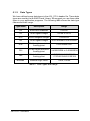
1
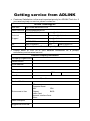
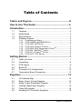
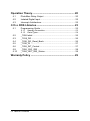
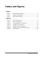
NuDAQ PCI-7258 PhotoMos Relay Cards User’s Guide Recycled Paper ©Copyright 2002 ADLINK Technology Inc. All Rights Reserved. Manual Rev: 1.04: October 18, 2002 Part NO: 50-11132-100 The information in this document is subject to change without prior notice in order to improve reliability, design and function and does not represent a commitment on the part of the manufacturer. In no event will the manufacturer be liable for direct, indirect, special, incidental, or consequential damages arising out of the use or inability to use the product or documentation, even if advised of the possibility of such damages. This document contains proprietary information protected by copyright. All rights are reserved. No part of this manual may be reproduced by any mechanical, electronic, or other means in any form without prior written permission of the manufacturer. Trademarks NuDAQ is registered trademarks of ADLINK Technology Inc. Other product names mentioned herein are used for identification purposes only and may be trademarks and/or registered trademarks of their respective companies. Getting service from ADLINK • Customer Satisfaction is the most important priority for ADLINK Tech Inc. If you need any help or service, please contact us. ADLINK Technology Inc. Web Site http://www.adlinktech.com Sales & Service [email protected] NuDAQ + USBDAQ [email protected] Technical Automation [email protected] Support NuIPC [email protected] NuPRO / EBC [email protected] TEL +886-2-82265877 FAX Address 9F, No. 166, Jian Yi Road, Chungho City, Taipei, 235 Taiwan. +886-2-82265717 • Please email or FAX us of your detailed information for a prompt, satisfactory and constant service. Detailed Company Information Company/Organization Contact Person E-mail Address Address Country TEL FAX Web Site Questions Product Model Environment to Use Detail Description Suggestions to ADLINK OS: Computer Brand: M/B: CPU: Chipset: BIOS: Video Card: Network Interface Card: Other: Table of Contents Tables and Figures................................................................iii How to Use This Guide.........................................................iv Introduction ..............................................................................1 1.1 1.2 1.3 1.4 Features ......................................................................... 2 Applications .................................................................... 2 Specifications ................................................................. 2 Software Support ............................................................ 4 1.4.1 1.4.2 1.4.3 1.4.4 1.4.5 1.4.6 1.4.7 1.4.8 Programming Library................................................................4 PCIS-LVIEW: LabVIEW® Driver............................................4 PCIS-VEE: VEE Driver............................................................5 PCIS-OCX: ActiveX Controls..................................................5 PCIS-DDE: DDE Server and InTouchTM...............................5 PCIS-ISG: ISaGRAFTM driver.................................................5 PCIS-ICL: InControlTM Driver..................................................6 PCIS-OPC: OPC Server..........................................................6 Getting Started ........................................................................7 2.1 2.2 2.3 2.4 2.6 2.7 What you have................................................................ 7 Unpacking ...................................................................... 8 PCB Layout .................................................................... 9 Board ID....................................................................... 11 Connector Pin Assignments........................................... 12 Termination Board Connection....................................... 13 Registers ................................................................................ 15 3.1 3.2 3.3 3.4 3.5 3.6 I/O Address Map ........................................................... 15 Relay Output Control Register ....................................... 16 Relay Output Read Back Register .................................. 17 Isolated Digital Input Register ........................................ 18 Clear IRQ register ......................................................... 18 Handling PCI Controller Registers .................................. 19 Table of Contents • i Operation Theory ................................................................. 20 4.1 4.2 4.3 PhotoMos Relay Output ................................................ 20 Isolated Digital Input ...................................................... 22 Interrupt Architecture..................................................... 22 C/C++ DOS Libraries ........................................................... 23 5.1 Programming Guide ...................................................... 23 5.1.1 5.1.2 5.2 5.3 5.4 5.5 5.6 5.9 5.10 Naming Convention................................................................23 Data Types...............................................................................24 _7258 Initial .................................................................. 25 _7258_DO.................................................................... 26 _7258_DO_Read_Back................................................. 26 _7258_DI ..................................................................... 27 _7258_INT_Control ....................................................... 27 _7258_CLR_IRQ .......................................................... 28 _7258_GET_IRQ_Status ............................................... 28 Warranty Policy .................................................................... 29 ii • Table of Contents Tables and Figures Tables Table 1. Board ID Setting Conditions ........................................................11 Table 2. Registers Address Map................................................................15 Table 3. Data Types and Range ................................................................24 Figures Figure 1: PCI-7258 PCB Layout....................................................................9 Figure 2: Board ID Dipswitch.......................................................................11 Figure 3: Pin Assignment of PCI-7258 CN1..............................................12 Figure 4: PhotoMos relay schematic..........................................................20 Figure 5: PhotoMos relay wiring diagram ..................................................21 Figure 6: Protection circuit for an Inductive load.......................................21 Figure 7: Photo-Coupler................................................................................22 Tables and Figures • iii How to Use This Guide This manual is intended to assist users to configure the PCI-7258 PhotoMos Relay Card. It is divided into 5 chapters. Chapter 1, “Introduction”, gives an overview of the product features, applications, and specifications. Chapter 2, “Getting Started”, describes how to install the PCI-7258. The Board ID switch and connectors’ pin assignments are also described. Chapter3, “Registers”, describes the registers that are available to the PCI-7258. The information is important for programmers who want to control the hardware with low level programming languages. Chapter 4, “Operation Theory”, describes how to operate the PCI7258. The PhotoMos relay and isolated digital input are introduced. Some programming concepts are also described. Chapter 5, “C/C++ libraries”, describes the software utility and the software libraries of the PCI-7258. This chapter also outlines basic requirements for programming your own software application. iv • How to Use This Guide 1 Introduction The PCI-7258 PhotoMos relay card is a basic Digital I/O card for PCI bus computers used in industrial applications. This PCI-7258 provides 32 PhotoMos relay actuators and 2 opto-isolated digital inputs. All relays are of Form A type and is very suited for constant ON/OFF control devices. Other useful feature includes the Board ID. It is convenient for board identification when two or more PCI-7258 cards are in a system. All I/O signals are routed via a 68-pin SCSI connector. Introduction • 1 1.1 Features The PCI-7258 PhotoMos relay actuator and D/I Card provides the following advanced features: • 32-bit PCI-Bus, Plug and Play • 32 PhotoMos relay actuator outputs • 2 opto-isolated digital inputs • On-board relay driving circuits • Digital input channel 0 & 1 interrupt • Board ID 1.2 Applications • Industrial ON/OFF control • Energy management • Laboratory automation • Industrial automation • Switch contact status sensing, limit switch monitoring, • Integrate with A/D and D/A cards to implement a data acquisition & control system 1.3 Specifications ♦ Digital input • Input channels: 2 • Photo-coupler: PC-3H4 • Input current: P 10 mA rated P 50 mA max. for isolated input 2 • Introduction • Input Voltage: P Up-to 24 VDC or 24V AC P Logic Low: 0~2V P Logic High 5~24V • Input impedance: 2.4 KΩ / 0.5W • Isolated voltage: 2,500 Vrms channel-to-system ♦ Relay Output • Output channels: 32 • Relay type: 32 SPST (Form A) • Load voltage (peak AC): 350V • Continuous load current (peak AC): 0.12A • Peak load current: 0.3A • I/O isolation voltage: 1,500 V AC • Output turn on resistance (typical): 17O • Output off state leakage current (Maximum): 1µ A • Turn on time (typical): 0.23 ms • Turn off time (typical): 0.04 ms ♦ General Specifications • Bus: 32-bit PCI bus • Dimension: 174 mm x 106 mm, standard PCI half size • Operating temperature: 0 ~ 60 °C • Storage temperature: -20 °C ~ 80 °C • Humidity: 5 to 95% non-condensing ♦ Power Consumption • +5V @ 380 mA (All relays energized) Introduction • 3 1.4 Software Support ADLINK provides versatile software drivers and packages for users’ different approach to building a system. ADLINK not only provides programming libraries such as DLL for most Windows based systems, but also provide ® TM TM drivers for other software packages such as LabVIEW , VEE , InTouch , TM TM InControl , ISaGRAF , and so on. All software options are included in the ADLINK CD. Non-free software drivers are protected with licensing codes. Without the software code, you can install and run the demo version for two hours for trial/demonstration purposes. Please contact ADLINK dealers to purchase the formal license. 1.4.1 Programming Library For customers who are writing their own programs, we provide function libraries for many different operating systems, including: • DOS Library: Borland C/C++ and Microsoft C++. Functional descriptions are included in this user’s guide • PCIS-DASK: Include device drivers and DLL for Windows 98, Windows NT and Windows 2000. DLL is binary compatible across Windows 98, Windows NT and Windows 2000. That means all applications developed with PCIS-DASK are compatible across Windows 98, Windows NT and Windows 2000. The developing environment can be VB, VC++, Delphi, BC5, or any Windows programming language that allows calls to a DLL. The user’s guide and function reference manual of PCIS-DASK are in the CD. Please refer the PDF manual files under \\Manual_PDF\Software\PCISDASK The above software drivers are shipped with the board. Please refer to the “Software Installation Guide” for installation procedures. 1.4.2 PCIS-LVIEW: LabVIEW® Driver ® PCIS-LVIEW contains the VIs, which is used to interface with NI’s LabVIEW software package. The PCIS-LVIEW supports Windows 95/98/NT/2000. The ® LabVIEW drivers is shipped free with the board. You can install and use them without a license. For more information about PCIS-LVIEW, please refer to the user’s guide in the CD. (\\Manual_PDF\Software\PCIS-LVIEW). 4 • Introduction 1.4.3 PCIS-VEE: VEE Driver The PCIS-VEE includes user objects, which are used to interface with the VEE software package. PCIS-VEE supports Windows 95/98/NT. The VEE drivers are shipped free with the board. You can install and use them without a license. For more information about PCIS-VEE, please refer to the user’s guide in the CD. (\\Manual_PDF\Software\PCIS-VEE). 1.4.4 PCIS-OCX: ActiveX Controls We suggest users who are familiar with ActiveX controls and VB/VC++ programming use the PCIS-OCX ActiveX control components library to develop their applications. PCIS-OCX is designed for Windows 98/NT/2000. For more information about PCIS-OCX, please refer to the user's guide in the CD. (\Manual_PDF\Software\PCIS-OCX\PCIS-OCX.PDF). The above software drivers are shipped with the board. Please refer to the “Software Installation Guide” for installation procedures. ADLINK also supply an ActiveX control software called DAQBench. DAQBench is a collection of ActiveX controls for measurement and automation applications. With DAQBench, you can develop custom user interfaces to display and analyze data you acquired or received from other sources, or integrate with popular applications or data sources. For more information about DAQBench, please refer to the user's guide in the CD. (\Manual_PDF\Software\DAQBench\DAQBenchManual.PDF). There is a free 4-hour evaluation version of DAQBench available in the CD. DAQBench is not free. Please contact ADLINK dealers or ADLINK to purchase the software license. 1.4.5 TM PCIS-DDE: DDE Server and InTouch DDE stands for Dynamic Data Exchange. The PCIS-DDE includes the PCI cards’ DDE server. The PCIS-DDE server is free and is included in the ADLINK CD. The DDE server can be used in conjunction with any DDE client under Windows 98/NT/2000. 1.4.6 PCIS-ISG: ISaGRAF TM driver The ISaGRAF Workbench is an IEC1131-3 SoftPLC control development environment. The PCIS-ISG includes ADLINK product drivers for ISaGRAF under Windows NT environment. The PCIS-ISG is included in the ADLINK CD. It is not free. Please contact ADLINK dealers or ADLINK to purchase the license. Introduction • 5 1.4.7 TM PCIS-ICL: InControl Driver PCIS-ICL is the InControl driver, which supports Windows NT. The PCIS-ICL is included in the ADLINK CD. It is not free and requires a license. Please contact ADLINK dealers or ADLINK to purchase the license. 1.4.8 PCIS-OPC: OPC Server PCIS-OPC is an OPC server, which can be used to link with other OPC clients. There are many software packages on the market that can provide the OPC clients. The PCIS-OPC supports Windows 98, NT, and 2000. It is not free. Please contact ADLINK dealers or ADLINK to purchase the license. 6 • Introduction 2 Getting Started This chapter describes how to install and setup the PCI-7258. The contents in the package and unpacking information that you should be aware of are outlined first. 2.1 What you have In addition to the User’s Manual, the package should include the following items: • PCI-7258 PhotoMos relay cards • ADLINK Software CD • Software Installation Guide If any of these items are missing or damaged, contact ADLINK or the dealer from whom you purchased the product. Save the shipping materials and carton in case you want to ship or store the product in the future. Getting Started • 7 2.2 Unpacking The card contains electro-static sensitive components that can be easily be damaged by static electricity. Therefore, the card should be handled on a grounded anti-static mat. The operator should be wearing an anti-static wristband, grounded at the same point as the anti-static mat. Inspect the card module carton for obvious damages. Shipping and handling may cause damage to your module. Be sure there are no shipping and handling damages on the modules carton before continuing. After opening the card module carton, extract the system module and place it only on a grounded anti-static surface with component side up. Again, inspect the module for damages. Press down on all the socketed IC's to make sure that they are properly seated. Do this only with the module place on a firm flat surface. Note: DO NOT ATTEMPT TO INSTALL A DAMAGED BOARD IN THE COMPUTER. You are now ready to install your card. 8 • Getting Started 2.3 PCB Layout The location of the connectors and switches on the PCI-7258 are shown in figure 1 below. Descriptions are o utline in the proceeding sections. Figure 1: PCI-7258 PCB Layout Getting Started • 9 2.4 External LED A K JP1 A K JP2 LED16 LED32 LED10 LED26 LED1 LED17 Figure 2: PCI-7258 External LED connector The PCI-7258 card is designed with 32 LEDs, each indicating the operation status of the 32 relays. In addition, there are also 32 external LED connectors available for users’ to use as so pleases. Utilizing the external LEDs connecting to JP1 or JP2, users can have a visual status of each relay displayed on a chassis, panel or on any apparatus. Only LED’s with a forward voltage (Vf) lower than 2V will operate. Each external LED connector has a current limiting resistor (330O ) connected to the +5V supply, therefore external current limiting circuitry for external LED’s are not necessary. The direction of the external LED’s connection is shown in Figure 2. Before connecting a LED to a connector, make sure the LED’s orientation is correct. 10 • Getting Started 2.5 Board ID When two or more data acquisition cards are installed in a system, it can be tedious trying to identify a specific card. For easier identification, the PCI7258 implemented a Board ID function. By setting the Dipswitch located at S1, users can assign an ID address to a specific card and access the card through software programming. For more details about the Board ID in programming, please refer to chapter 5. Table 1 below shows all dipswitch setting conditions. ON 1 Figure 3: 2 3 4 Board ID Dipswitch Switch No. Board ID 1 1 0 1 0 1 0 1 0 1 0 1 0 1 0 1 0 0 (default) 1 2 3 4 5 6 7 8 9 10 11 12 13 14 15 2 1 1 0 0 1 1 0 0 1 1 0 0 1 1 0 0 3 1 1 1 1 0 0 0 0 1 1 1 1 0 0 0 0 4 1 1 1 1 1 1 1 1 0 0 0 0 0 0 0 0 Table 1. Board ID Setting Conditions Note: 1=on, 0=off Getting Started • 11 2.6 Connector Pin Assignments The PCI-7258 card is equipped with a 68-pin SCSI connector (CN1). Figure 3 defines the pin assignment for the connector. NO1 COM1 NO2 COM2 NO3 COM3 NO4 COM4 NO5 COM5 NO6 COM6 NO7 COM7 NO8 COM8 NO9 COM9 NO10 COM10 NO11 COM11 NO12 COM12 NO13 COM13 NO14 COM14 NO15 COM15 NO16 COM16 NO17 COM17 Figure 4: 1 2 3 4 5 6 7 8 9 10 11 12 13 14 15 16 17 18 19 20 21 22 23 24 25 26 27 28 29 30 31 32 33 34 NO18 COM18 NO19 COM19 NO20 COM20 NO21 COM21 NO22 COM22 NO23 COM23 NO24 COM24 NO25 COM25 NO26 COM26 NO27 COM27 NO28 COM28 NO29 COM29 NO30 COM30 NO31 COM31 NO32 COM32 DIO DI1 DIGND0 DIGND1 Pin Assignment of PCI-7258 CN1 Legend: NO x: Relay normal open pin x, x = 1~32 COM x: Relay common pin x, x = 1~32 DI x: Digital input pin x, x = 0~1 DIGND x: Digital input ground pin x, x = 0~1 12 • Getting Started 35 36 37 38 39 40 41 42 43 44 45 46 47 48 49 50 51 52 53 54 55 56 57 58 59 60 61 62 63 64 65 66 67 68 2.7 Termination Board Connection The available termination board for the 68-pin SCSI connector is the DIN68S/1S. The DIN-68S/1S is a general-purpose 68-pin screw terminal with a DIN socket. It is also equipped with a 68-pin SCSI cable that allows for easy installation of the PCI-7258. Getting Started • 13 3 Registers Detailed descriptions of the registers are specified in this chapter. This information is useful for programmers who wish to handle the card with lowlevel programming. However, we suggest users to have an understanding of the PCI interface before starting any low-level programming. 3.1 I/O Address Map The PCI-7258 registers are all 16-bits long. Users can access these registers by 16-bit I/O instructions only. The controls for the relays and status of the isolated inputs are by means of accessing these registers. The following table shows the registers mapping addresses; the addresses are offset relative to the base address. Offset Write Read 0x00h Relay Output CH. 1~16 Relay Output Read back CH.1~16 0x02h Relay Output CH. 17~32 Relay Output Read back CH.17~32 0x04h --- Isolated Input CH. 0, 1 0x08h Clear IRQ --- Table 2. Registers Address Map Registers • 15 3.2 Relay Output Control Register There are 32 PhotoMos relays on the PCI-7258; each bit of the register corresponds to a relay channel. Writing “1” to the register will cause the relay to close and “0” will cause it to open. Address: BASE + 0x00 Attribute: Write 7 6 5 4 3 2 1 0 RLY8 RLY7 RLY6 RLY5 RLY4 RLY3 RLY2 RLY1 15 14 13 12 11 10 9 8 RLY16 RLY15 RLY14 RLY13 RLY12 RLY11 RLY10 RLY9 Address: BASE + 0x02 Attribute: Write 7 6 5 4 3 2 1 0 RLY24 RLY23 RLY22 RLY21 RLY20 RLY19 RLY18 RLY17 15 14 13 12 11 10 9 8 RLY32 RLY31 RLY30 RLY29 RLY28 RLY27 RLY26 RLY25 RLYx: relay output channel x, x=1~32 16 • Registers 3.3 Relay Output Read Back Register The status of the PhotoMos relay can be read back from the readback register. If the relay is in the close position, the corresponding bit value is ‘1’. If the relay is open, then the bit value is ‘0’. Address: BASE + 0x00 Attribute: Read 7 6 5 4 3 2 1 0 RBK8 RBK7 RBK6 RBK5 RBK4 RBK3 RBK2 RBK1 15 14 13 12 11 10 9 8 RBK16 RBK15 RBK14 RBK13 RBK12 RBK11 RBK10 RBK9 Address: BASE + 0x02 Attribute: Read 7 6 5 4 3 2 1 0 RBK24 RBK23 RBK22 RBK21 RBK20 RBK19 RBK18 RBK17 15 14 13 12 11 10 9 8 RBK32 RBK31 RBK30 RBK29 RBK28 RBK27 RBK26 RBK25 RBKx: Read back data of relay x, x=1~32 Registers • 17 3.4 Isolated Digital Input Register There are 2 isolated input channels on PCI-7258 card. The status of the 2 channels can be read from the isolated input register. Each bit corresponds to each channel. A “1” means the input logic is high and “0” means the input logic is low. Address: BASE + 0x04 Attribute: Read 7 6 5 4 3 2 1 0 --- --- --- --- --- --- DI1 DI0 15 14 13 12 11 10 9 8 --- --- --- --- --- --- --- --- DIx: isolated digital input channel x, x=0, 1 3.5 Clear IRQ register The PCI-7258 has two interrupt sources for the digital input channels 0 and 1. Writing anything to this register will clear the interrupt request. Address: BASE + 0x08 Attribute: Write 7 6 5 4 3 2 1 0 --- --- --- --- --- --- --- --- 15 14 13 12 11 10 9 8 --- --- --- --- --- --- --- --- 18 • Registers 3.6 Handling PCI Controller Registers The PCI bus controller adopted in PCI-7258 is the PCI-9030, which is provided by PLX technology Inc. When users attempt to handle low-level programming, some registers in the PCI-9030 should be noticed. The interrupt control register (INTCSR; 0x4Ch) of the PCI-9030 takes charge of all interrupt information from the local bus to PCI bus. When users want to develop their own interrupt function driver, both interrupt registers in the PCI9030 and in PCI-7258 have to work together. For more information about the interrupt control register in the PCI-9030, refer to the PCI-9030 data book. With the PCI-7258 software function library, ADLINK has provided simple and easy-to-use functions to handle the procedures of interrupts. Using these functions, users are not required to know about the interrupt register in the PCI controller. Hence, we recommend users use these functions instead of developing your own interrupt functions. For more information about the PCI7258 function library, refer to Chapter 5. Registers • 19 4 Operation Theory 4.1 PhotoMos Relay Output The PhotoMos relay has LED inputs and MOSFET outputs that provide inputoutput isolation. When a signal current flows into the LED input pin, the emitted light from the LED is detected by the photoelectric element (solar cell), which is mounted opposite to the LED. The photoelectric element then converts the received light to a voltage, which charges the MOSFET gate on the output side. When the voltage reaches a preset voltage value, the MOSFET begins to conduct and turns on the load. The simplified circuit of PhotoMos relay is shown in figure 4 below. Figure 5: 20 • Operation Theory PhotoMos relay schematic The PhotoMos relay incorporates the advantages of both a semiconductor and an electro-mechanical relay. The PhotoMos relay utilizes the MOSFET as a switch instead of the mechanical contact. Thus the contact resistance remains stable through the life of the relay. Furthermore, dithering problems is eliminated. The PCI-7258 is equipped with 32 PhotoMos relays, which are all form A type. The load voltage can either be AC or DC. The basic wiring diagram is shown in figure 5 below. Figure 6: PhotoMos relay wiring diagram If an inductive load is connected, the spike voltage may exceed the relay’s maximum rating. To protect the components, user should add a diode in the circuit. A typical protection circuit is shown below. Figure 7: Protection circuit for an Inductive load Operation Theory • 21 4.2 Isolated Digital Input The PCI-7258 contains 2 opto-isolated digital input channels. The circuit diagram of the isolated input channel is shown below. 2.4 KO DI DIGND Figure 8: Photo-Coupler The digital input is routed through a photo-coupler (PC3H4), so that the connections are not polarity sensitive whether using positive or negative voltages. The PCI-7258 digital input has an inline 2.4kO resistor and the input voltage can ranges from 0 to 24V. 4.3 Interrupt Architecture PCI-7258 has a powerful dual interrupt routing scheme and the interrupt sources are on the digital input channels 0 and 1. Using these interrupts will make handling complicated digital information much easier and relief your computer from the heavy burden of dealing with digital input data. Note that dual interrupts does not mean the card occupies two IRQ levels. The interrupt will occur only when digital input level changes from 0 to 1. In other words, the interrupt condition occurs on the rising edge, triggered on the DI channel. Be sure to clear the interrupt request after handling the ISR or the next interrupt request will not be received normally. For more information about the interrupt operation, refer to section 5.6. 22 • Operation Theory 5 C/C++ DOS Libraries This chapter describes the software libraries for operating this card. The function prototypes and useful constants are defined in the header files located in the LIB and INCLUDE directory. 5.1 Programming Guide 5.1.1 Naming Convention The functions of the NuDAQ PCI or NuIPC CompactPCI card software drivers uses full-names to represent the functions' real meaning. The naming convention rules are: _{hardware_model}_{action_name}. e.g. _7258_Initial(). All functions in the PCI-7258 drivers are with 7258 as {hardware_model}. C/C++ Libraries • 23 5.1.2 Data Types We have defined some data types in the ACL_PCI.h header file. These data types are used by the NuDAQ Cards’ library. We suggest you use these data types in your application programs. The following table shows the data type names and their range. Type Name Description Range U8 8-bit ASCII character 0 to 255 I16 16-bit signed integer -32768 to 32767 U16 16-bit unsigned integer 0 to 65535 I32 32-bit signed integer -2147483648 to 2147483647 U32 32-bit single-precision floating-point 0 to 4294967295 F32 32-bit single-precision floating-point -3.402823E38 to 3.402823E38 F64 64-bit double-precision floating-point -1.797683134862315E308 to 1.797683134862315E309 Boolean Boolean logic value TRUE, FALSE Table 3. Data Types and Range 24 • C/C++ Libraries 5.2 _7258 Initial @ Description The PCI-7258 cards are initialized according to the card number. Because the PCI-7258 is designed with the PCI bus architecture and meets the plug and play specifications, the IRQ and base_address (pass-through address) are assigned by system BIOS directly. Every PCI-7258 card has to be initialized by this function before using any other functions. @ Syntax U16 _7258_Initial (U16 *existCards, PCI_INFO *pciInfo) @ Argument existCards: The number of installed PCI-7258 cards. The returned value shows how many PCI-7258 cards are installed in the system. pciInfo: This structure stores the PCI bus plug and play initialization information which is determined by PnP BIOS. The PCI_INFO structure is defined in the ACL_PCI.H header file. The base I/O addresses and the interrupt channel number are stored in the pciinfo, which is used for reference. @ Return Code ERR_NoError, ERR_PCIBiosNotExist, ERR_BoardNoInit, ERR_InvalidBoardNumber C/C++ Libraries • 25 5.3 _7258_DO @ Description @ Syntax U16 _7258_DO (U16 boardID, U16 Group, U16 doData) @ Argument boardID: Board ID for the specific board. Group: group 0 represents DO channel 1~16, group 1 represents DO channel 17~32. doData: value which will be written to digital output port. @ Return Code ERR_NoError, ERR_BoardNoInit, ERR_InvalidDOChannel 5.4 _7258_DO_Read_Back @ Description This function is used to read data back from the digital output port controlled by the 7258_DO function. You can read back all relay status (close or open) by using this function. @ Syntax U16 _7258_DO_Read_Back (U16 boardID, U16 Group, U16 *doReadBackData) @ Argument boardID : Board ID for the specific board. Group: group 0 represents DO channel 1~16, group 1 represents DO channel 17~32. diReadBackData : Value read back from digital output port. ‘0’ represents the PhotoMos relay is under open condition and ‘1’ represents the PhotoMos relay is under close condition. @ Return Code ERR_NoError, ERR_BoardNoInit, ERR_InvalidDOChannel 26 • C/C++ Libraries 5.5 _7258_DI @ Description This function is used to read data from the digital input port. There are 2 bits in the Isolated Digital Input Register for digital inputs purposes. You can read the input data by using this function. @ Syntax U16 _7258_DI (U16 boardID, U16 *diData) @ Argument boardID : Board ID for the specific board. diData : return 16-bit value from digital input port. Only last 2 bit data are valid. @ Return Code ERR_NoError, ERR_BoardNoInit 5.6 _7258_INT_Control @ Description This function is used to control the interrupt source of the PCI-7258. The interrupt source can be the digital input of channel 0, 1 or both. @ Syntax U16 _7258_INT_Control (U16 boardID, U16 int1Flag, U16 int2Flag) @ Argument boardID: Board ID for the specific board. Int1Flag: Digital input channel 0 interrupt control, “1” enable and “0” disable. Int2Flag: Digital input channel 1 interrupt control, “1” enable and “0” disable. @ Return Code ERR_NoError, ERR_BoardNoInit C/C++ Libraries • 27 5.9 _7258_CLR_IRQ @ Description This function is used to clear the interrupt request. @ Syntax U16 _7258_CLR_IRQ (U16 boardID) @ Argument boardID: Board ID for the specific board. @ Return Code ERR_NoError, ERR_BoardNoInit 5.10 _7258_GET_IRQ_Status @ Description This function is used to obtain the interrupt status. @ Syntax U16 _7258_GET_IRQ_Status (U16 boardID, U16 *int1Status, U16 *int2Status) @ Argument boardID: Board ID for the specific board. Int1Status: interrupt source 0 status, “1” represents interrupt request assert and “0” represents interrupt request de-assert. Int2Status: interrupt source 1 status, “1” represents interrupt request assert and “0” represents interrupt request de-assert. @ Return Code ERR_NoError, ERR_BoardNoInit 28 • C/C++ Libraries Warranty Policy Thank you for choosing ADLINK. To understand your rights and enjoy all the after-sales services we offer, please read the following carefully. 1. Before using ADLINK’s products, please read the user manual and follow the instructions carefully. When sending in damaged products for repair, please attach an RMA application form. 2. All ADLINK products come with a two-year guarantee, free of repair charge. 3. 4. • The warranty period starts from the product’s shipment date from ADLINK’s factory • Peripherals and third-party products not manufactured by ADLINK will be covered by the original manufacturers’ warranty • End users requiring maintenance services should contact their local dealers. Local warranty conditions will depend on the local dealers Our repair service does not cover the two-year guarantee while damages are caused by the following: a. Damage caused by not following instructions in the u ser menus. b. Damage caused by carelessness on the users’ part during product transportation. c. Damage caused by fire, earthquakes, floods, lightening, pollution and incorrect usage of voltage transformers. d. Damage caused by unsuitable storage environments with high temperatures, high humidity or volatile chemicals. e. Damage caused by leakage of battery fluid when changing batteries. f. Damages from improper repair by unauthorized technicians. g. Products with altered and damaged serial numbers are not entitled to our service. h. Other categories not protected under our guarantees. Customers are responsible for the fees regarding transportation of damaged products to our company or to the sales office. Warranty Policy • 29 5. To ensure the speed and quality of product repair, please download an RMA application form from our company website www.adlinktech.com . Damaged products with RMA forms attached receive priority. For further questions, please contact our FAE staff. ADLINK: [email protected] Test & Measurement Product Segment: [email protected] Automation Product Segment: [email protected] Computer & Communication Product Segment: [email protected]; [email protected] 30 • Warranty Policy