1
USER’S GUIDE
Date
: 25 October 2006
Doc. no. : Bridge_UG
Iss./Rev : 1.1
Page
:1
User’s Guide
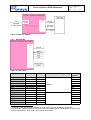
Parallel Bus to IEEE1394 Bridge
(using the UC1394a-1 MCM with Generic Streaming BSP)
Orsys Orth System GmbH, Am Stadtgraben 25, 88677 Markdorf, Germany
http://www.orsys.de
USER’S GUIDE
PARALLEL BUS TO IEEE1394 BRIDGE
Date
: 25 October 2006
Doc. no. : Bridge_UG
Iss./Rev : 1.1
Page
:2
Contents
1 PREFACE...................................................................................................................... 8
1.1
Document Organization ......................................................................................................... 8
1.2
Documentation Overview ...................................................................................................... 8
1.3
Notational Conventions ......................................................................................................... 8
1.4
Trademarks ............................................................................................................................. 9
1.5
Revision History ................................................................................................................... 10
2 SYSTEM OVERVIEW .................................................................................................. 11
2.1
Virtual Connection Protocol ................................................................................................ 12
2.2
Streaming Port...................................................................................................................... 13
2.3
UART Interface ..................................................................................................................... 13
2.4
Host Port Interface (HPI)...................................................................................................... 13
2.5
I/O Pins .................................................................................................................................. 13
2.6
IEEE1394 Interface ............................................................................................................... 13
2.7
Power Supply........................................................................................................................ 14
2.8
Configuration........................................................................................................................ 14
2.9
LEDs ...................................................................................................................................... 14
2.10
Diagnostic Interface ........................................................................................................... 14
2.11
Configuration Interface...................................................................................................... 14
2.12
Registration Interface ........................................................................................................ 14
3 DETAILED INTERFACE DESCRIPTION .................................................................... 15
3.1 Streaming Port...................................................................................................................... 15
3.1.1 Streaming Port Signals........................................................................................................ 15
3.1.2 Streaming Port Operation.................................................................................................... 19
3.1.3 Controlling Streaming Port Operation over VCP ................................................................. 20
3.1.4 Streaming Port Configuration .............................................................................................. 21
3.2 UART ..................................................................................................................................... 24
3.2.1 UART Signals...................................................................................................................... 25
3.2.2 UART Configuration ............................................................................................................ 26
3.3
Host Port Interface (HPI)...................................................................................................... 28
USER’S GUIDE
PARALLEL BUS TO IEEE1394 BRIDGE
3.3.1
3.3.2
3.3.3
Date
: 25 October 2006
Doc. no. : Bridge_UG
Iss./Rev : 1.1
Page
:3
HPI Signals.......................................................................................................................... 29
HPI Configuration ................................................................................................................ 31
HPI Registers (Host Side) ................................................................................................... 34
3.4 I/O Pins .................................................................................................................................. 39
3.4.1 I/O Pin Signals..................................................................................................................... 41
3.4.2 I/O Pin Alternative Functions ............................................................................................... 41
3.4.3 I/O Pin Startup State Options .............................................................................................. 42
3.4.4 I/O Pin Configuration ........................................................................................................... 43
3.5 Diagnostic Interface ............................................................................................................. 44
3.5.1 Diagnostic Interface over IEEE1394 ................................................................................... 45
3.5.2 Diagnostic Interface over Dedicated I/O Pins...................................................................... 45
3.5.3 Diagnostic Interface over the HPI........................................................................................ 46
3.5.4 Diagnostic Interface over the LED....................................................................................... 46
3.5.5 Description of Available Error Codes .................................................................................. 47
3.5.6 Description of Available Detailed Error Codes .................................................................... 48
3.5.7 Diagnostic Interface Configuration ...................................................................................... 49
3.6 Configuration Interface........................................................................................................ 50
3.6.1 Configuration Interface Configuration.................................................................................. 51
3.6.2 Configuration Interface Usage............................................................................................. 51
3.7 Registration Interface .......................................................................................................... 51
3.7.1 Registration Interface Configuration .................................................................................... 51
3.8 IEEE1394 Interface ............................................................................................................... 51
3.8.1 IEEE1394 Data Transfer Methods ...................................................................................... 51
3.8.2 IEEE1394 Cable Power Option ........................................................................................... 53
4 CONFIGURATION....................................................................................................... 53
4.1 Configuration Mode ............................................................................................................. 53
4.1.1 Customized Configuration ................................................................................................... 54
4.2
Configuration Tool ............................................................................................................... 55
4.3 Common Device Parameters............................................................................................... 55
4.3.1 Device ID (dev_id)............................................................................................................... 56
4.3.2 Default Partner Device (partner_dev).................................................................................. 56
4.3.3 FPGA Version (fpga_ver) .................................................................................................... 56
4.3.4 FPGA Revision (fpga_rev) .................................................................................................. 56
4.3.5 Software Version (sw_ver) .................................................................................................. 56
4.3.6 Software Revision (sw_rev)................................................................................................. 57
4.3.7 VCP Version (vcp_ver)........................................................................................................ 57
5 VIRTUAL CONNECTION PROTOCOL ....................................................................... 57
5.1
Accessing the UC1394a-1 MCM Using the VCP SDK........................................................ 58
5.2
Using VCP Without the SDK................................................................................................ 60
6 HARDWARE IMPLEMENTATION GUIDELINES........................................................ 61
USER’S GUIDE
PARALLEL BUS TO IEEE1394 BRIDGE
Date
: 25 October 2006
Doc. no. : Bridge_UG
Iss./Rev : 1.1
Page
:4
6.1
Power Supply........................................................................................................................ 61
6.2
IEEE1394 Interface ............................................................................................................... 61
6.3
Configuration Mode ............................................................................................................. 63
6.4
Device and Partner ID from I/O Pins ................................................................................... 64
6.5
RS-232 Level-Converter....................................................................................................... 65
6.6
JTAG Interface...................................................................................................................... 65
6.7
Unused Signals .................................................................................................................... 66
6.8
Minimal Connection Example ............................................................................................. 66
7 TECHNICAL DATA ..................................................................................................... 68
7.1
Connector Pinout Tables ..................................................................................................... 68
7.2 Individual Signal Description .............................................................................................. 71
7.2.1 Power Supply and Reset Signals ........................................................................................ 71
7.2.2 Streaming Port Signals........................................................................................................ 71
7.2.3 I/O Pins, Host Port and Diagnostic Interface ....................................................................... 72
7.2.4 UART Signals...................................................................................................................... 72
7.2.5 IEEE1394 Signals ............................................................................................................... 73
7.2.6 McBSP Signals.................................................................................................................... 73
7.2.7 JTAG Signals ...................................................................................................................... 73
7.2.8 External Flag ....................................................................................................................... 75
7.2.9 Analog Inputs ...................................................................................................................... 75
7.2.10 USB Signals ...................................................................................................................... 75
7.2.11 I2C Signals......................................................................................................................... 75
7.3
Dimensions of the UC1394a-1............................................................................................. 76
7.4 Environmental Conditions................................................................................................... 76
7.4.1 Storage................................................................................................................................ 76
7.4.2 Ambient Humidity ................................................................................................................ 76
7.4.3 Ambient Temperature.......................................................................................................... 77
7.5
Soldering Process................................................................................................................ 77
7.6
Power Requirements............................................................................................................ 77
7.7 Signal Levels and Loads ..................................................................................................... 78
7.7.1 I/O Pin Signals..................................................................................................................... 78
7.7.2 Streaming Port Signals........................................................................................................ 78
7.7.3 UART Signals...................................................................................................................... 79
7.7.4 Reset Signals ...................................................................................................................... 79
7.7.5 Other Signals....................................................................................................................... 80
7.8 Signal Timings...................................................................................................................... 80
7.8.1 Streaming Port Timings ....................................................................................................... 80
7.8.2 HPI Timings ......................................................................................................................... 83
7.8.3 I/O Pin Timings .................................................................................................................... 84
USER’S GUIDE
PARALLEL BUS TO IEEE1394 BRIDGE
7.8.4
Date
: 25 October 2006
Doc. no. : Bridge_UG
Iss./Rev : 1.1
Page
:5
Reset Timing ....................................................................................................................... 85
7.9 Predefined Configuration Tables ........................................................................................ 85
7.9.1 Configuration Mode 0 (31 KBps Predefined Configuration) ................................................ 86
7.9.2 Configuration Mode 1 (313 KBps Predefined Configuration) .............................................. 88
7.9.3 Configuration Mode 2 (3 MBps Predefined Configuration).................................................. 90
7.9.4 Configuration Mode 3 (15 MBps Predefined Configuration)................................................ 92
7.9.5 Configuration Mode 4 (31 MBps Predefined Configuration)................................................ 94
7.9.6 Configuration Mode 5 (31 KBps Predefined Configuration) ................................................ 96
7.9.7 Configuration Mode 6 (313 kBps Predefined Configuration) ............................................... 98
7.9.8 Configuration Mode 7 (3 MBps Predefined Configuration)................................................ 100
7.9.9 Configuration Mode 8 (15 MBps Predefined Configuration).............................................. 102
7.9.10 Configuration Mode 9 (31 MBps Predefined Configuration)............................................ 104
7.9.11 Configuration Mode 10 .. 13 (Reserved) and 14 .. 15 (Factory Default).......................... 106
8 LIST OF ABBREVIATIONS AND ACRONYMS USED IN THIS DOCUMENT.......... 108
9 LITERATURE REFERENCES................................................................................... 108
USER’S GUIDE
PARALLEL BUS TO IEEE1394 BRIDGE
Date
: 25 October 2006
Doc. no. : Bridge_UG
Iss./Rev : 1.1
Page
:6
List of Tables
Table 1: Streaming port connector pin assignments ....................................................................... 16
Table 2: streaming port parameter overview................................................................................... 22
Table 3: streaming port transfer bandwidth examples .................................................................... 22
Table 4: UART connector pin assignments..................................................................................... 25
Table 5: UART parameter overview ................................................................................................ 26
Table 6: HPI connector pin assignments......................................................................................... 30
Table 7: Available functions for /HRDY_/HRRDY ........................................................................... 31
Table 8: HPI parameter overview.................................................................................................... 32
Table 9: HPI address map in 16-bit configuration ........................................................................... 34
Table 10: HPI address map in 8-bit configuration ........................................................................... 35
Table 11: HPI register layout in 16-bit configuration ....................................................................... 35
Table 12: HPI register layout in 8-bit configuration ......................................................................... 35
Table 13: I/O pin assignments......................................................................................................... 41
Table 14: I/O pin parameter overview ............................................................................................. 43
Table 15: Diagnostics interface pin assignments ............................................................................ 46
Table 16: Available error codes....................................................................................................... 47
Table 17: Available detailed error codes ......................................................................................... 49
Table 18: Diagnostic interface parameter overview ........................................................................ 50
Table 19: Available configuration modes ........................................................................................ 54
Table 20: Common device parameters overview ............................................................................ 55
Table 21: Pinning of the IEEE1394 connectors............................................................................... 61
Table 22: IEEE1394 connector part numbers ................................................................................. 61
Table 23: Required cable connection to a host PC ......................................................................... 65
Table 24: Pinout sorted by pins....................................................................................................... 68
Table 25: Power supply and reset signals....................................................................................... 69
Table 26: Streaming port signals..................................................................................................... 69
Table 27: I/O pin signals.................................................................................................................. 69
Table 28: UART interface signals.................................................................................................... 69
Table 29: DSP JTAG signals........................................................................................................... 69
Table 30: HPI signals ...................................................................................................................... 70
Table 31: Diagnostic signals ........................................................................................................... 70
Table 32: IEEE1394 signals ............................................................................................................ 70
Table 33: power requirements......................................................................................................... 77
Table 34: Signal levels and loads for I/O pins I/O[11:0] and I/O[26:15] .......................................... 78
Table 35: Signal levels and loads for I/O pins I/O[14:12] ................................................................ 78
Table 36: Signal levels and loads for the streaming port signals (STR_xxx) .................................. 79
Table 37: Signal levels and loads for the UART interface signals (UART_xxx) .............................. 79
Table 38: /RESET_IN signal levels ................................................................................................. 79
Table 39: /RESET_OUT signal levels ............................................................................................. 79
Table 40: Streaming port transmit timing parameters ..................................................................... 80
Table 41: Streaming port receive timing parameters ...................................................................... 81
Table 42: Maximum achievable streaming bandwidths................................................................... 82
Table 43: Streaming port transmit timing parameters (imaging mode) ........................................... 83
Table 44: HPI write timing parameters ............................................................................................ 83
Table 45: HPI read timing parameters ............................................................................................ 84
Table 46: I/O pin timings for single I/O pin virtual connection ......................................................... 85
Table 47: I/O pin timings for virtual connection with 8 I/O pins ...................................................... 85
Table 48: Reset timing .................................................................................................................... 85
Table 49: Differences between the predefined & passive parameter sets ...................................... 85
Table 50: Predefined configuration mode 0 .................................................................................... 87
Table 51: Predefined configuration mode 1 .................................................................................... 89
Table 52: Predefined configuration mode 2 .................................................................................... 91
Table 53: Predefined configuration mode 3 .................................................................................... 93
USER’S GUIDE
PARALLEL BUS TO IEEE1394 BRIDGE
Date
: 25 October 2006
Doc. no. : Bridge_UG
Iss./Rev : 1.1
Page
:7
Table 54: Predefined configuration mode 4 .................................................................................... 95
Table 55: Predefined configuration mode 5 .................................................................................... 97
Table 56: Predefined configuration mode 6 .................................................................................... 99
Table 57: Predefined configuration mode 7 .................................................................................. 101
Table 58: Predefined configuration mode 8 .................................................................................. 103
Table 59: Predefined configuration mode 9 .................................................................................. 105
Table 60: Passive configuration .................................................................................................... 107
List of Figures
Figure 1: Parallel bus to IEEE1394 Bridge overview....................................................................... 11
Figure 2: Bridge block diagram ....................................................................................................... 12
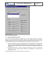
Figure 3 VCP demo application....................................................................................................... 13
Figure 4: Streaming port block diagram .......................................................................................... 15
Figure 5: Streaming port signals in generic mode........................................................................... 16
Figure 6: Streaming port signals in imaging mode .......................................................................... 16
Figure 7: UART interface block diagram ......................................................................................... 25
Figure 8: UART signals ................................................................................................................... 25
Figure 9: HPI block diagram............................................................................................................ 29
Figure 10: HPI signals ..................................................................................................................... 29
Figure 11: I/O pin block diagram ..................................................................................................... 39
Figure 12: I/O pin configurations ..................................................................................................... 40
Figure 13: Example for a virtual connection between two I/O pins ................................................. 40
Figure 14: Diagnostic interface block diagram ................................................................................ 45
Figure 15: Diagnostic interface over I/O pins .................................................................................. 46
Figure 16: Isochronous data, recorded from the IEEE1394 bus with an analyzer .......................... 52
Figure 17: Isochronous packet assembly, sampling at 100kHz, 16bit, packet size = 40 bytes....... 52
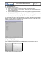
Figure 18: Configuration tool ........................................................................................................... 55
Figure 19: Virtual connection between two hardware interfaces..................................................... 57
Figure 20: Virtual connection between a host PC and a hardware interface .................................. 58
Figure 21: VCP SDK structure ........................................................................................................ 59
Figure 22: VCP demo application.................................................................................................... 60
Figure 23: 6-pin IEEE1394 connectors ........................................................................................... 62
Figure 24: 4-pin IEEE1394a connector ........................................................................................... 62
Figure 25: Pin numbering for 6-pin and 4-pin IEEE1394 connectors (top view) ............................. 62
Figure 26: Supplying the MCM from IEEE1394 .............................................................................. 62
Figure 27: Supplying power to the IEEE1394 cable........................................................................ 63
Figure 28: Minimum required wiring for customized configuration .................................................. 63
Figure 29: Alternative wiring for customized configuration.............................................................. 64
Figure 30: Setting device and partner ID over I/O pins ................................................................... 64
Figure 31: Wiring of UART interface ............................................................................................... 65
Figure 32: Wiring of the DSP JTAG interface.................................................................................. 66
Figure 33: Required connections .................................................................................................... 67
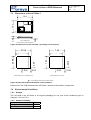
Figure 34: Dimensions of the UC1394a-1 (including connector pins) ............................................. 76
Figure 35: Recommended PCB footprint of the UC1394a-1 ........................................................... 76
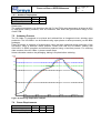
Figure 36: Soldering temperature example ..................................................................................... 77
Figure 37: Streaming port transmit timing ....................................................................................... 80
Figure 38: Streaming port receive timing ........................................................................................ 81
Figure 39: Streaming port transmit timing (imaging mode) ............................................................. 82
Figure 40: HPI write timing .............................................................................................................. 83
Figure 41: HPI read timing .............................................................................................................. 84
USER’S GUIDE
PARALLEL BUS TO IEEE1394 BRIDGE
Date
: 25 October 2006
Doc. no. : Bridge_UG
Iss./Rev : 1.1
Page
:8
1 Preface
This document describes the Parallel Bus to IEEE1394 Bridge that is implemented on the
UC1394a-1 multi-chip-module. It is intended for first-time users as well as for users that want to
migrate from the Parallel Bus to IEEE1394 Bridging Kit to a customized solution.
1.1
Document Organization
This document is organized as follows:
• Chapter 2 gives a brief overview of the module and its interfaces.
• Chapter 3 describes each interface in detail.
• Chapter 4 describes how to configure the module.
• Chapter 5 describes the protocol that is used for communication between modules.
• Chapter 6 shows how to integrate the module in custom hardware.
• Chapter 7 lists the technical data of the module.
• Chapter 8 explains the abbreviations used in this document
• Chapter 9 contains a list of reference documents that contain further information.
1.2
Documentation Overview
This chapter lists the documentation from Orsys that is shipped together with the Parallel Bus to
IEEE1394 Bridge. Further documents from other vendors are listed in chapter 9 and are
referenced throughout the document in square brackets.
Parallel Bus to IEEE1394 Bridge User's Guide (Bridge_UG.pdf):
(= this document) Describes the function of the UC1394a-1 MCM when equipped with the
streaming board support package (BSP). This is the recommended starting point for reading.
Parallel Bus to IEEE1394 Bridging Kit User's Guide [1] (Bridging_Kit_UG.pdf):
Describes the Bridging Kit (Complete system for quick and easy start with the UC1394a-1 mounted
on a Carrier board). Listed here for reference only.
Protocol specification Virtual Connection Protocol [3] (vcp_spec.pdf)
Describes the protocol that is used for communication over IEEE1394. Required for advanced
programming with the VCP SDK or for own VCP implementations on embedded systems or
non-Windows® environments.
Virtual Connection Protocol API [7] (VCPrefman.pdf):
Describes how to use the Windows®-based VCP SDK. Required for software development on a
Windows-based PC.
1.3
Notational Conventions
Names of registers, bit fields and single bits are written in capital letters.
Example: LLC_VERSION
Names of signals are also given in capital letters, active low signals are marked with a '/' at the
beginning of the name.
Example: /RESETIN
Configuration parameters and function names are written in italic typeface.
Example: dev_id
source code examples are given in a small, fixed-width typeface.
Example: int a = 10;
Date
: 25 October 2006
Doc. no. : Bridge_UG
Iss./Rev : 1.1
Page
:9
USER’S GUIDE
PARALLEL BUS TO IEEE1394 BRIDGE
The members of a bit field or a group of signals are numbered starting at zero, which is the least
significant bit.
Example: CFG[4:0] identifies a group of five signals, where CFG0 is the least significant bit and
CFG4 is the most significant bit.
If necessary, numbers are represented with a suffix that specifies their base.
Example: 12AB16 is a hexadecimal number (base 16 = hexadecimal) and is equal to 477910.
The bit fields of a register are displayed with the most significant bit to the left. Below each bit field
is a description of its read / write accessibility and its default value:
bit name
bit number
15
14
13
12
11
10
6
5
4
3
2
1
0
A
B
C
D
E
F
9
G
8
7
H
I
J
K
L
N
O
r,w,0
r,w,0
r,w,0
r,w,0
r,w,0
r,w,0
r,w,0102
r,0
r,wc,0
w
r,w,0
rc,0
r,w,0
r,w,0
accessibility and default value
legend:
r = bit is readable
w = bit is writeable
(r),(W) = bit is readable and writeable, but has different meanings for read and write (can't be read
back).
rc = this bit is cleared after a read
wc = writing a '1' to this bit clears it
0 = default value
1.4
Trademarks
TI, Code Composer, DSP/BIOS and TMS320C5000 are registered trademarks
of Texas Instruments.
Microsoft® and Windows® are either registered trademarks or
trademarks of Microsoft Corporation in the United States and/or other
countries.
All other brand or product names are trademarks or registered trademarks of
the respective companies or organizations.
USER’S GUIDE
PARALLEL BUS TO IEEE1394 BRIDGE
1.5
Revision History
Revision
1.0
1.1
Date
: 25 October 2006
Doc. no. : Bridge_UG
Iss./Rev : 1.1
Page
: 10
Changes
First issue. Replaces Generic_Streaming_Kit_PnP.pdf and GS_BSP_PnP.pdf
Required FPGA Version: V4.08 or higher
Required firmware version / revision: V2.01 or higher
Required VCP version: 1.4
Table I/O pin states for configuration mode corrected.
Minor typos corrected.
UART & HPI Tx packet size: suggested value and description revised.
UART & HPI Tx timeout: suggested value reduced to 100ms, max. value added.
str_ch=receive all: also not allowed for VCP usage.
Module and footprint dimensions revised.
New error code added (supported in firmware V2.6 or higher).
Cross-referenced footnotes reformatted (were missing in the PDF version).
Updated to RoHS compliant production.
Documentation overview: exchanged document names corrected.
Implementation guidelines for IEEE1394 connectors revised.
Minimum pulse width specification for MCM-internal reset on /RESETIN removed.
Configuration mode overview: auto start vs. manual start corrected (was exchanged).
UART interface: Rx/Tx FIFO mentioned.
USER’S GUIDE
PARALLEL BUS TO IEEE1394 BRIDGE
Date
: 25 October 2006
Doc. no. : Bridge_UG
Iss./Rev : 1.1
Page
: 11
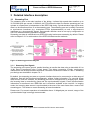
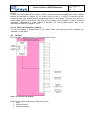
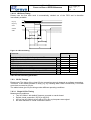
2 System Overview
The Parallel bus to IEEE1394 Bridge is a ready-to-use solution for interfacing an 8 bit or 16 bit
parallel port (called streaming port throughout this document) to the IEEE1394 bus. The bridge
also provides some auxiliary interfaces:
•
•
•
up to 27 general purpose I/O pins
an UART interface
a 8/16 bit host port interface
The bridge is implemented on a UC1394a-1 Multi Chip Module (MCM) that is equipped with the
generic streaming Board Support Package (BSP). High level access to the hardware interfaces
over IEEE1394 is provided by the Orsys Virtual Connection Protocol (VCP). A VCP SDK for
Windows® based PCs provides easy development of application software. Interface configuration
and communication parameters can be adjusted and permanently stored in the MCM's Flash
memory using a configuration tool.
The UC1394a-1 MCM is designed for end application use. It can be directly integrated into
customer hardware, allowing mass production with small form factor and low cost. For easy system
integration, a bridging kit is available as a separate product, providing quick and easy start by
using a carrier board that provides all necessary connectors and power supply [1].
For applications that require a customized version of the bridge, various development kits for
software and FPGA development are available.
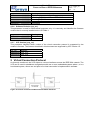
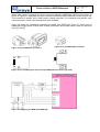
Figure 1: Parallel bus to IEEE1394 Bridge overview
USER’S GUIDE
PARALLEL BUS TO IEEE1394 BRIDGE
Date
: 25 October 2006
Doc. no. : Bridge_UG
Iss./Rev : 1.1
Page
: 12
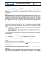
Figure 2: Bridge block diagram
2.1
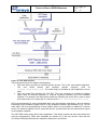
Virtual Connection Protocol
The Virtual Connection Protocol (VCP) is an interface based protocol for connecting two or more
devices over the IEEE1394 bus. Each of the device's interfaces can be connected to an interface
of the same type on a remote device using a virtual connection over IEEE1394. On a Windows®
based host PC, the VCP SDK provides access to these interfaces on API level. For the first steps a
VCP demo application is included in the SDK. This demo application uses a graphical user
interface for accessing the interfaces of remote devices.
USER’S GUIDE
PARALLEL BUS TO IEEE1394 BRIDGE
Date
: 25 October 2006
Doc. no. : Bridge_UG
Iss./Rev : 1.1
Page
: 13
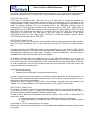
Figure 3 VCP demo application
The VCP defines device IDs and interface instances for addressing. The interface instance
enumerates interfaces of the same type, such as I/O pins. A virtual connection can be made
between any two interfaces of the same type on any two devices on the IEEE1394 network. For
example, I/O pin 5 on device 0 can use I/O pin 3 on device1 as a 'partner interface' and vice versa.
This defines a virtual connection between the two I/O pins.
2.2
Streaming Port
The streaming port is the main interface of the bridge. It allows unidirectional high speed data
transfers of up to 32,768,000 bytes per second. The interface is built as a 8 or 16 bit parallel
interface that can be accessed by external hardware using either synchronous or asynchronous
access timings. Streaming data is FIFO-buffered, so that external hardware can operate
independent of the IEEE1394 bus. A detailed description of the streaming port can be found in
chapter 3.1.
2.3
UART Interface
The UART interface is used for two purposes. It can be used for device configuration using a host
PC running the configuration tool, or it can be used as a general purpose UART interface, e.g. for
command and status exchange between the bridge and external hardware. A detailed description
of the UART interface can be found in chapter 3.2.
2.4
Host Port Interface (HPI)
The Host port interface is a parallel 8 or 16 bit interface, intended for low to medium speed control
and status exchange with an external host. Transfer bandwidths strongly depend on IEEE1394 bus
traffic and allow up to around 500KBps. The HPI supports dynamic addressing, so that different
devices can be addressed by the host without reconfiguration. A detailed description of the HPI
can be found in chapter 3.3.
2.5
I/O Pins
The UC1394a-1 MCM has up to 27 general purpose I/O pins available. They can be configured
and used individually and are intended for low speed, bit level I/O. Maximum switching speed
strongly depends on IEEE1394 bus traffic and is around 1kHz. A detailed description of the I/O
pins can be found in chapter 3.4.
2.6
IEEE1394 Interface
The UC1394a-1 MCM has two 400Mbps IEEE1394 ports. The IEEE1394 interface connects the
bridge to other devices, such as other bridges or host PCs. During IEEE1394 bus enumeration, the
bridge identifies itself as a device running the Virtual Connection Protocol (VCP). This guarantees
USER’S GUIDE
PARALLEL BUS TO IEEE1394 BRIDGE
Date
: 25 October 2006
Doc. no. : Bridge_UG
Iss./Rev : 1.1
Page
: 14
interoperability with other IEEE1394 devices and allows a Windows® based host PC to recognize
the bridge. The host PC will then automatically load the appropriate high-level driver which is
included in the VCP SDK.
2.7
Power Supply
The UC1394a-1 MCM requires a single, regulated 3.3 V power supply. See chapter 7.6 for details.
2.8
Configuration
Operation of the UC1394a-1 MCM can be adjusted by a set of parameters, one for each interface
plus one set of common device parameters. Adjusting the parameters is done by a configuration
tool using the UART interface. The UC1394a-1 MCM also has some predefined parameter sets,
that can be selected by the startup state of certain I/O pins. Device configuration is described in
chapter 4.
A second method for configuration exists over the configuration interface. See chapter 3.6.
2.9
LEDs
The red LED of the UC1394a-1 MCM is used as a part of the diagnostic interface to indicate error
conditions by a blink code. The blink codes are described in chapter 3.5.5.
2.10 Diagnostic Interface
The diagnostic interface is not an interface for data transfer. Instead, it is used for troubleshooting
when things don't work as expected. In end application environment the diagnostic interface can
be used to collect long-term statistics. Errors and warnings that appear during operation are stored
in an error FIFO, together with the interface they're related to and some classification flags. The
error FIFO can be read out by a virtual connection from anywhere in the IEEE1394 network.
Severe error conditions can be signaled to local hardware through dedicated I/O pins or through
the host port interface. Local hardware can use these mechanisms to detect potential problems
and take the appropriate action. A third mechanism for signaling error conditions is the red LED. It
signals errors through a blink code. The diagnostic interface is described in chapter 3.5.
2.11 Configuration Interface
The configuration interface is a software-only interface that allows to configure the bridge over
IEEE1394. It is intended for situations where operating parameters must be adjusted at runtime,
e.g. when two bursts of streaming data have to be transferred using different bandwidths (packet
sizes). How to use the configuration interface is described in chapter 3.6.
2.12 Registration Interface
The registration interface is a software-only interface that allows non-VCP devices to access the
interfaces of a VCP device. The registration interface is described in chapter 3.7.
USER’S GUIDE
PARALLEL BUS TO IEEE1394 BRIDGE
Date
: 25 October 2006
Doc. no. : Bridge_UG
Iss./Rev : 1.1
Page
: 15
3 Detailed Interface description
3.1
Streaming Port
The streaming port is the main interface of the bridge. It allows high speed data transfers up to
32,768,000 bytes per second. A 2048x161 bit FIFO buffers the data, so that the streaming port can
operate at a speed that is independent of the IEEE1394 timing. Synchronization flags signal when
data is to be transferred from or to the streaming port. The streaming port can be easily connected
to synchronous interfaces (e.g. customized FPGA implementations) as well a asynchronous
interfaces (e.g. microcontroller buses). Data transfer direction must be set up by configuration or
over VCP before streaming operation is started.
Streaming port data is transferred over IEEE1394 using isochronous streaming by default. Please
refer to chapter 3.8.1 for a discussion of the IEEE1394 data transfer methods.
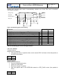
Figure 4: Streaming port block diagram
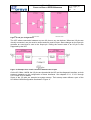
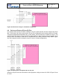
3.1.1 Streaming Port Signals
The streaming port uses a generic, parallel interface to transfer the data using a data width of 8 or
16 bit. Data is transferred using a clock signal. This allows connection of both, synchronous
interfaces as well as asynchronous interfaces. Connector locations are listed in Table 1. Streaming
port timings are described in chapter 7.8.1.
By default, the streaming port acts as a generic interface that can be connected to a wide range of
interfaces. Data will be transferred transparently, without further information. For use with image
data sources, such as cameras, the streaming port can be configured as an imaging input, where
the incoming data is controlled by frame and line synchronization signals. Frame synchronization
information is transferred over IEEE1394 and is therefore available at the receiver. In imaging
mode, the incoming data stream is synchronized to the start of the next frame after a reset of the
streaming port. This allows to restart streaming at frame boundaries.
Please note: For transmit operation at bandwidths above 10 Megabytes per second, usage of the
synchronization flags is strongly recommended.
1
The FIFO has an output register which increases the FIFO size to 2049 words.
USER’S GUIDE
PARALLEL BUS TO IEEE1394 BRIDGE
Figure 5: Streaming port signals in generic
mode
Signal
Generic
Imaging
STR_D0
CAM_D0
STR_D1
CAM_D1
STR_D2
CAM_D2
STR_D3
CAM_D3
STR_D4
CAM_D4
STR_D5
CAM_D5
STR_D6
CAM_D6
STR_D7
CAM_D7
STR_D8
CAM_D8
STR_D9
CAM_D9
STR_D10
CAM_D10
STR_D11
CAM_D11
STR_D12
CAM_D12
STR_D13
CAM_D13
STR_D14
CAM_D14
STR_D15
CAM_D15
STR_CLK
CAM_PCLK
/STR_WE
CAM_FEN
/STR_RE
CAM_LEN
/STR_FLAG0 /CAM_FLAG0
/STR_FLAG1 /CAM_FLAG1
Date
: 25 October 2006
Doc. no. : Bridge_UG
Iss./Rev : 1.1
Page
: 16
Figure 6: Streaming port signals in imaging mode
MCM connector pin
B3
B4
B5
B6
B7
B8
B9
B10
B12
B13
B14
B15
B16
B17
B18
B19
B23
B21
B22
B24
B25
Table 1: Streaming port connector pin assignments
STR_D[15:0], CAM_D[15:0]
These are the data lines of the streaming port. They carry 8 or 16 bit of streaming data between
user hardware and the IEEE1394 network. If the streaming port is configured for receiving data
from the IEEE1394 network, STR_D[15:0] are tri-state outputs, controlled by /STR_RE. Image
mode is not allowed for receive direction. When configured for 8-bit receive operation,
STR_D[15:8] are always driven low. In transmit direction, STR_D[15:0] or CAM_D[15:0] are inputs.
USER’S GUIDE
PARALLEL BUS TO IEEE1394 BRIDGE
Date
: 25 October 2006
Doc. no. : Bridge_UG
Iss./Rev : 1.1
Page
: 17
/STR_WE
When the streaming port is configured for generic interface mode and transmit direction (from the
streaming port to the IEEE1394 network), /STR_WE is used to write data into the transmit FIFO of
the streaming port. Data on STR_D[15:0] is clocked in with each rising edge of STR_CLK. If the
FIFO can no longer accept data (indicated by a high level on /STR_FLAG0), because it is full, any
data written to it will be ignored. /STR_WE is ignored when the streaming port is configured for
receive operation.
/STR_RE
When the streaming port is configured for generic interface mode and receive direction (from
IEEE1394 network to the streaming port), /STR_RE is used to read data from the receive FIFO of
the streaming port. Data on STR_D[15:0] is driven while /STR_RE is active (low). If the receive
FIFO is empty (no data has yet been received), the data on STR_D[15:0] is invalid. The first data
received from the IEEE1394 network will be automatically read out of the FIFO and its availability
will be indicated by /STR_FLAG0. This means the first read operation already reads out the first
data word, without any clock required. This feature is similar to the 'first word fall through' mode of
discrete FIFO components.
CAM_FEN
When the streaming port is configured for imaging interface mode and transmit direction (from the
streaming port to the IEEE1394 network), CAM_FEN is the (high-active) frame enable signal that
indicates that a picture frame is currently being transferred. An active CAM_FEN signal has two
effects:
• A rising edge of CAM_FEN causes that the current data is transferred with the
synchronization information.
• CAM_FEN works as a clock enable, thus data can only be written to the streaming port,
when CAM_FEN is active (high). Together with CAM_LEN, CAM FEN works as a clock
enable for CAM_PCLK.
For correct transmission of synchronization information, CAM_FEN must be inactive (low) between
two picture frames
•
•
for at least 1 period of STR_PCLK if str_tx_pktsize is set to 4096 bytes
4096
for at least int⎛ str_packet_size ⎞ * 125 µs for other settings of str_tx_pktsize
⎝
⎠
See chapter 3.1.4.1 for a description of configuration parameter str_tx_pktsize
Example:
str_tx_pktsize is set to 520 bytes (= 4,160,000MBps).
4096
Required idle time between two picture frames: = int⎛ 520 ⎞ * 125 µs = int( 7.877 ) * 125 µs =
⎝
⎠
7 * 125 µs = 875 µs
When the streaming port is configured for imaging interface mode and receive direction,
CAM_FEN will be ignored and no streaming operation is possible.
CAM_LEN
When the streaming port is configured for imaging interface mode and transmit direction (from the
streaming port to the IEEE1394 network), CAM_LEN is the (high-active) line enable signal that
indicates that one line of a picture frame is currently being transferred. Together with CAM_FEN it
enables that data is clocked into the streaming port. Data can only be clocked into the streaming
USER’S GUIDE
PARALLEL BUS TO IEEE1394 BRIDGE
Date
: 25 October 2006
Doc. no. : Bridge_UG
Iss./Rev : 1.1
Page
: 18
port when CAM_LEN is active (high). When the streaming port is configured for imaging interface
mode and receive direction, CAM_FEN will be ignored and no streaming operation is possible.
STR_CLK, CAM_PCLK
Clock input for streaming data. With each clock, one data word is transferred between the
streaming port interface and external hardware. When the streaming port is configured as an
imaging interface, CAM_PCLK is the pixel clock. All timings of the streaming port are related to this
clock. In transmit direction (from the streaming port to the IEEE1394 network), data on
STR_D[15:0] or CAM_D[15:0] is clocked in with each rising edge of STR_CLK / CAM_PCLK. In
receive direction (from IEEE1394 network to the streaming port), a falling edge on STR_CLK while
/STR_RE is low causes the next data to be clocked out of the FIFO, while the current data at
STR_D[15:0] is being held. The new data of the FIFO output is transferred to the output
(STR_D[15:0]) after the next rising edge of STR_CLK. Connected hardware should sample
STR_D[15:0] at the rising edge of STR_CLK.
/STR_FLAG0, /CAM_FLAG0
This signal is active low. It works as a synchronization flag for word-synchronized data transfers.
Data can only be transferred from / to the streaming port while /STR_FLAG0 or /CAM_FLAG0 is
low.
In receive direction (from IEEE1394 network to the streaming port), a low level on /STR_FLAG0
indicates that at least one 16-bit data word is available at the streaming port. This is independent of
the configured streaming port data width. Therefore, in 16-bit configuration, one data word is
available and in 8-bit mode two data words are available.
In transmit direction (from the streaming port to the IEEE1394 network), a low level on
/STR_FLAG0 or /CAM_FLAG0 indicates that the streaming port's FIFO can accept at least one
more 16-bit data word. This is independent of the configured streaming port data width. Therefore,
in 16-bit configuration, the FIFO can accept at least one more data word and in 8-bit mode it can
accept at least two more data words.
This signal can be used as
• synchronization flag
• underrun/overrun indicator for unsynchronized transfers
In case of isochronous transfers (which is the default transfer method for the streaming port), the
FIFO gets filled or emptied with each isochronous cycle (every 125µs). See also chapter 3.8.1 for a
description of isochronous packetizing.
Please note: Due to timing of /STR_FLAG0, only transfers of limited speed are possible (see
chapter 7.8.1 for timing details). For full speed transfers, /STR_FLAG1 must be used.
/STR_FLAG1, /CAM_FLAG1
This signal is active low. It works as a synchronization flag for block-synchronized data transfers.
A low level on /STR_FLAG1 or /CAM_FLAG1 indicates that one more block of data can be
transferred between external hardware and the streaming port.
A block of data is defined by configuration parameter str_blksize. /STR_FLAG1 or /CAM_FLAG1 is
active (low), when
a) streaming direction is receive and the FIFO holds at least str_blksize data.
b) streaming direction is transmit and the FIFO has free space for at least str_blksize
data.
See chapter 3.1.4.10 for a description of str_blksize.
Please note: The behavior of this signal is not affected by the configured streaming port data width
(str_width).
USER’S GUIDE
PARALLEL BUS TO IEEE1394 BRIDGE
Date
: 25 October 2006
Doc. no. : Bridge_UG
Iss./Rev : 1.1
Page
: 19
A typical use of /STR_FLAG1 is to set the block size to 4 bytes and to check /STR_FLAG1 after
every second access (in 16 bit configuration). This provides a quadlet based synchronization which
can be used for transfers at full speed.
3.1.2
Streaming Port Operation
3.1.2.1 Streaming Port Word / Byte Order
On the IEEE1394 interface, streaming port data is transferred in units of quadlets (32-bit words).
Most significant parts of a quadlet are transferred first. Therefore, when receiving a quadlet of data
from the IEEE1394 bus, Bit[31:16] (16-bit interface width) or Bit[31:24] (8-bit interface width) are
the first data that can be read at the streaming port.
3.1.2.2 Streaming Port Packetizing
It is important to know, that streaming port data is transferred in packets of fixed sizes. The packet
size is always defined by the transmitter and affects streaming port transmit operation as follows:
Data only gets sent if enough data for one packet is available. If exactly one 16-bit word is written
to the streaming port (configured for transmit direction), no data is sent on the IEEE1394 interface,
since the amount of data is less that the minimum packet size of 4 bytes. The transmitted data
must be a multiple of the configured transmit packet size (see configuration parameter
str_tx_pktsize in chapter 3.1.4.1). Otherwise, the reaming data stays in the streaming port's
transmit FIFO forever.
For isochronous streaming, which is the default transfer method, transmit operation is further
limited to one packet each 125µs.
See also chapter 3.8.1 for further information.
3.1.2.3 Streaming Port Synchronization
Streaming port data transfers can be synchronized by using /STR_FLAG0 and /STR_FLAG1.
Synchronization is required
• for receive operation in general
• for transmit operation at high bandwidths
3.1.2.4 Streaming Port Synchronization in Receive Direction
In receive direction, /STR_FLAG0 or /STR_FLAG1 must be checked to be active before data is
read out of the streaming port. Otherwise a FIFO underrun error will occur. The code example
below shows how to check for receive data, assuming that the UC1394a-1 MCM is connected to a
micro-line C6x11CPU module as follows:.
• /STR_FLAG0 connected to interrupt /INT0
• /STR_FLAG1 connected to interrupt /INT1
• /STR_RE connected to /CS1
• /STR_CLK connected to /IOSTRB
/* single word-synchronized transfers */
#define STR_RX_DATA_AVAIL ((C6X11CPU_INT_STAT & C6X11CPU_ISR_INT0) != 0)
#define STR_READ
(*(volatile INT32U *)(C6X11CPU_CS1_BASE)))
/* wait for data */
while(!STR_RX_DATA_AVAIL);
/* read data from streaming port */
pBuffer++ = STR_READ;
/* block-synchronized transfers */
#define STR_RX_BLOCK_AVAIL ((C6X11CPU_INT_STAT & C6X11CPU_ISR_INT1) != 0)
#define STR_READ
(*(volatile INT32U *)(C6X11CPU_CS1_BASE)))
#define STR_BLKSIZE 10 /* 10 bytes = 5 16-bit words. Note: MCM must be configured accordingly! */
/* wait for next data block */
while(!STR_RX_BLOCK_AVAIL);
/* read one block of data from the streaming port */
USER’S GUIDE
PARALLEL BUS TO IEEE1394 BRIDGE
Date
: 25 October 2006
Doc. no. : Bridge_UG
Iss./Rev : 1.1
Page
: 20
for (i = 0; i < STR_BLKSIZE; i++)
pBuffer++ = STR_READ;
Please note: Due to the flag timing, data transfer bandwidth is limited when /STR_FLAG0 is
checked before each access. Therefore, for operation with STR_CLK frequencies above 10 MHz,
block based synchronization with /STR_FLAG1 is required.
When using /STR_FLAG1 for synchronization, streaming port operation should follow these
guidelines:
• Starting and stopping transfer on the externally connected hardware must be done at block
boundaries only.
• Before resetting the streaming port over VCP, the external hardware must be stopped.
3.1.2.5 Streaming Port Synchronization in Transmit Direction
In transmit direction, data written to the streaming port is buffered in the streaming port's FIFO until
at least str_tx_pktsize bytes are available. Only then, the IEEE1394 chipset start arbitrating for
transmission. For isochronous streaming, transmission starts at the next isochronous cycle.
Therefore, the FIFO must be able to buffer one packet plus a little bit more than 125 µs, provided
that data is written to the streaming port without synchronization. The resulting bandwidths and
packet size limits are listed in chapter 7.8.1.1.5.
In order to use higher bandwidths, data may only be written to the streaming port if the FIFO has
free space. The code example below shows how to implement this on a micro-line C6x11CPU
module with the following connections:
• /STR_FLAG1 connected to interrupt /INT1
• /STR_WE connected to /CS2
• /STR_CLK connected to /IOSTRB
/* block-synchronized transmit transfer */
#define STR_TX_BLOCK_FREE ((C6X11CPU_INT_STAT & C6X11CPU_ISR_INT1) != 0)
#define STR_WRITE(data)
*(volatile INT32U *)(C6X11CPU_CS2_BASE)) = data
#define STR_BLKSIZE 1024 /* 1024bytes=512 16-bit words. Note: MCM must be configured accordingly! */
/* wait for >= 1 block of free space in FIFO */
while(!STR_TX_BLOCK_FREE);
/* write one block of data to the streaming port */
for (i = 0; i < STR_BLKSIZE; i++)
STR_WRITE(*pBuffer++);
Please note: Due to the flag timing, data transfer bandwidth is limited when /STR_FLAG0 is
checked before each access. Therefore, for operation with STR_CLK frequencies above 10 MHz,
block based synchronization with /STR_FLAG1 is required.
When using /STR_FLAG1 for synchronization, streaming port operation should follow these
guidelines:
• Starting and stopping transfer on the externally connected hardware must be done at block
boundaries only.
• Before resetting the streaming port over VCP, the external hardware must be stopped.
3.1.3 Controlling Streaming Port Operation over VCP
Streaming operation can be controlled over VCP. The configured partner interface can control the
following aspects of streaming operation:
• start and stop of streaming operation
• reset of the streaming port
• direction of the streaming transfer
3.1.3.1 Start and Stop of Streaming Operation
Starting and stopping streaming transfers controls the data transfer between the FIFO and the
IEEE1394 chipset. In transmit direction, operation is started and stopped at packet boundaries in
order to prevent invalid packets on the IEEE1394 interface. Receive operation is started and
stopped immediately.
USER’S GUIDE
PARALLEL BUS TO IEEE1394 BRIDGE
Date
: 25 October 2006
Doc. no. : Bridge_UG
Iss./Rev : 1.1
Page
: 21
Controlling streaming port operation in this way allows to implement a simple flow control
mechanism.
When streaming operation is stopped, data is still transferred between external hardware and the
streaming port FIFO. In transmit direction, external hardware will fill the FIFO until it is stopped by a
high level on /STR_FLAG0 or /STR_FLAG1. If no handshake is used, the FIFO will overflow.
In receive direction, external hardware can read out the remaining data from the FIFO. If the
hardware is not synchronized by /STR_FLAG0 or /STR_FLAG1, an underflow condition will be
generated.
Depending on the application and the connected hardware, it may be necessary to reset the
streaming port prior to restarting streaming operation. This clears the FIFO from previous data.
When the streaming port is operated in imaging mode, especially when /STR_FLG[1:0] are not
used, a reset must be performed before restarting after a stop. This triggers synchronization to the
next start of a picture frame.
With the VCP SDK, start and stop of streaming can be done by the functions
VCP_StartStreaming() / VCP_StopStreaming().
3.1.3.2 Resetting the Streaming Port
Resetting the streaming port causes the following actions
• The streaming port's FIFO is cleared
• Transmission is stopped at the next packet boundary
• error flags are cleared
• the streaming port is set up with the current operation parameters
• 8-bit operation: 8/16 bit conversion is reset to start with the MSB
• imaging mode: synchronization to the next picture frame is triggered
3.1.3.3 Changing Transfer Direction of the Streaming Port
This feature allows to implement time-multiplexed bi-directional transfers. For changing the
direction, the following sequence is necessary:
•
•
•
•
•
•
stop streaming operation
stop the external hardware
change transfer direction of the external hardware
change transfer direction at the streaming port
reset the streaming port
start streaming operation at the connected hardware
Controlling the external hardware (enable/disable, direction) can be implemented, for example, by
using I/O pins.
3.1.4 Streaming Port Configuration
Operation of the streaming port is affected by a number of configuration parameters. These
parameters can be adjusted using the UART interface and the configuration tool or over VCP.
Table 2 lists all parameters for the streaming port, sorted by importance. The subsequent sections
describe the streaming port parameters. The configuration process is described in chapter 4.
Parameter name
str_tx_pktsize
str_dir
str_ch
str_xfertype
str_partner_dev
str_partner_inst
str_width
Meaning
bandwidth / packet size
transfer direction for streaming data
channel number
transfer method
partner device for streaming
partner instance (interface number) on the partner device
data width
USER’S GUIDE
PARALLEL BUS TO IEEE1394 BRIDGE
Parameter name
str_iftype
str_auto
str_blksize
str_frmsync
Date
: 25 October 2006
Doc. no. : Bridge_UG
Iss./Rev : 1.1
Page
: 22
Meaning
identifies the type of hardware interface on the streaming port
auto-start feature
transfer block size on streaming port interface
synchronization bit pattern for frame start (imaging interface only)
Table 2: streaming port parameter overview
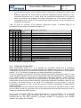
3.1.4.1 Streaming Port Transmit Bandwidth / Packet Size (str_tx_pktsize)
This parameter defines the amount of data that can be transmitted in one second. Since data is
transferred in packets, the packet size defines the transmit bandwidth. For receive operation, the
bandwidth can't be adjusted since it is defined by the transmitter. The packet size is expressed in
terms of bytes, however, only multiples of 4 bytes are allowed. Table 3 shows the relationship
between packet size and bandwidth. The bandwidth must be set so that it is never exceeded. A
good choice is to set the bandwidth 20% higher than the maximum data rate at the streaming port.
str_tx_pktsize
(bytes)
4
8
12
16
32
64
128
256
512
1024
2048
4096
Bandwidth
(bytes per second)
32,000
64,000
96,000
128,000
256,000
512,000
1,024,000
2,048,000
4,096,000
8,192,000
16,384,000
32,768,000
Table 3: streaming port transfer bandwidth examples
3.1.4.2 Streaming Port Direction (str_dir)
This parameter defines the transfer direction of the streaming port. The direction must be
configured, since the streaming port can transfer data in one direction only. str_dir can be set to
• Receive (from IEEE1394 to streaming port).
• Transmit (from streaming port to IEEE1394).
• Direction determined by the startup state of I/O26.
The UC1394a-1 MCM allows to define the streaming port direction by the startup state of one of its
I/O pins (I/O26). When I/O26 is high at system startup, streaming direction will be set to transmit.
Otherwise, direction will be set to receive.
Please note that the streaming port direction can also be controlled over VCP at runtime (see
chapter 3.1.3.3).
3.1.4.3 Streaming Port Channel (str_ch)
This parameter identifies the data stream within the IEEE1394 network. str_ch identifies the
outgoing data stream or is used to filter out incoming data streams. For isochronous streaming
(which is the default transfer method for the streaming port), str_ch determines the isochronous
channel number. It can be set to
USER’S GUIDE
PARALLEL BUS TO IEEE1394 BRIDGE
•
•
•
Date
: 25 October 2006
Doc. no. : Bridge_UG
Iss./Rev : 1.1
Page
: 23
a value of 0 .. 632
receive all channels (not allowed for transmit or for use with the VCP SDK)
derive the channel number ID from other configuration parameters as follows:
transmit direction:
channel number is equal to configuration parameter dev_id
receive direction:
channel number is equal to configuration parameter str_partner_dev
Configuration parameters dev_id and str_partner_dev are described in chapters 4.3.1 and 3.1.4.5
respectively.
Suggested default value for str_ch is to derive the channel number automatically from other
configuration parameters.
Please note: the configuration tool displays str_ch as "stream Id".
3.1.4.4 Streaming Port Transfer Method
This parameter defines, how streaming port data is transferred over IEEE1394. Currently
implemented are
•
•
isochronous streaming
asynchronous streaming (affects transmit operation only).
Please note that asynchronous streaming is different from asynchronous transactions.
Asynchronous transactions are currently not implemented for the streaming port. A description of
the transfer methods can be found in chapter 3.8.1.
3.1.4.5 Streaming Port Partner Device (str_partner_dev)
This parameter defines the device that is used as partner for the streaming port. The partner
device is allowed to control streaming operation of the local device by writing to the STR_CTL
software register (see [3] for details). This allows to control streaming operation as described in
chapter 3.1.3.
str_partner_dev can be set to:
• The device ID of a remote device (0 .. 6210).
• Accept any device as partner.
• Use configuration parameter partner_dev from the device-global parameters (see chapter
4.3.2).
Suggested default value for this parameter is to use configuration parameter partner_dev from the
device-global parameters.
3.1.4.6 Streaming Port Partner Interface Instance (str_partner_inst)
This parameter is used when multiple streaming ports exist on a device. It defines which streaming
port of the partner device is used as partner for the streaming port. Together with str_partner_dev,
str_partner_inst acts as a filter for incoming streaming start / streaming stop events over VCP.
For isochronous streaming (which is the default transfer method for the streaming port), no other
function is associated with this parameter. str_partner_inst can be set to:
• A interface instance (number of the streaming port) between 0 and 255.
• Accept any streaming port of the partner device.
Suggested default value for this parameter is interface instance 0, since there is usually only one
streaming port per device.
2
A stream ID of 3110 is reserved by the IEEE1394 standard and should not be used
USER’S GUIDE
PARALLEL BUS TO IEEE1394 BRIDGE
Date
: 25 October 2006
Doc. no. : Bridge_UG
Iss./Rev : 1.1
Page
: 24
3.1.4.7 Streaming Port Data Width (str_width)
This parameter controls the number of data bits of the streaming port (number of supported
STR_Dx lines. The data width is given in bits. It can be set to
• 8-bit interface: one byte per clock is transferred on the streaming port, STR_D[7:0] are
used, STR_D[15:8] are ignored for transmit operation and set to 0016 for receive operation.
• 16-bit interface: one 16-bit word per clock is transferred on the streaming port. All data lines
(STR_D[15:0]) are used.
Please note that when 8-bit operation is configured, the maximum data rate is limited. See chapter
7.8.1.1.5 for details.
3.1.4.8 Streaming Port Interface Type(str_iftype)
This parameter controls the function of the streaming port signals. It can be set to
• generic interface: external hardware accesses the streaming port word-by word using
asynchronous or synchronous timing.
• imaging interface: external hardware writes data to the streaming port using a pixel clock
and frame / line enable signals. Only valid for transmit operation.
Please refer to chapter 3.1.1 for a description of the interface types.
3.1.4.9 Streaming Port Startup Behavior (str_auto)
This parameter decides, whether streaming operation is automatically started after system startup
(set to auto-start), or if streaming must be enabled by the partner device (manual start). Streaming
control by the partner device is always possible, independent of str_auto. The suggested default
value for this parameter is to use manual start, especially when a PC with the VCP SDK is used as
partner device.
3.1.4.10 Streaming Port Block Size (str_blksize)
This parameter defines the block size for transfers between the streaming port and external
hardware (independent of the packet size on the IEEE1394 network). str_blksize is specified in
bytes. However, only multiples of two bytes are allowed. Minimum block size is two bytes,
maximum block size is 4096 bytes (equal to the FIFO size). In receive direction, a low level on
/STR_FLAG1 or /CAM_FLAG1 signals the availability of (at least) one block of data. In transmit
direction, a low level on /STR_FLAG1 or /CAM_FLAG1 signals that the streaming port can accept
(at least) one more block of data from external hardware. Block based data transfers are faster
than single-word transfers, since the availability of data (or space for data) needs only the be
checked once per block. See also chapters 3.1.1 and 3.1.2.3 for details on /STR_FLAG1 behavior.
3.1.4.11 Streaming Port Frame Synchronization Pattern (str_frmsync)
This parameter is used when the streaming port is configured as an imaging interface (see
str_iftype). The first packet of a frame contains the str_frmsync bit pattern in its header (sy field;
see [4]). All other packets have the synchronization bits cleared. When the streaming port is
configured as a generic interface, all packets will have the sync pattern defined by this parameter
in their header. Frame synchronization requires a minimum inactive time for the CAM_FEN signal
(see description of the CAM_FEN signal above). Allowed values for the sync pattern are 0 .. F16.
Application software on the receiver side can use this feature to synchronize to an already running
data stream.
3.2
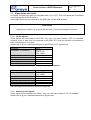
UART
The UC1394a-1 MCM has an UART interface that can be used for standard asynchronous
communication. Different baud rates are supported as well as RTS/CTS handshake. The signals of
the UART interface operate with LVTTL logic levels, therefore a level converter is required for
usage as an RS-232 interface (see chapter 6.5 for details). Incoming and outgoing characters are
buffered by a 16-character FIFO. The virtual connections use a software buffer and event-based
flow control.
USER’S GUIDE
PARALLEL BUS TO IEEE1394 BRIDGE
Date
: 25 October 2006
Doc. no. : Bridge_UG
Iss./Rev : 1.1
Page
: 25
The UART interface is also used for device configuration. To enable UART configuration, the
UC1394a-1 MCM must have UART configuration enabled. This is done by selecting configuration
mode 1510 of the MCM. The configuration mode is determined by the startup state of I/O pins
IO[25:22] as shown in chapter 6.3. Please refer to chapter 4 for information about device
configuration. Please note that the UART interface is not available for virtual connections when it is
used for configuration. Incoming UART data is then interpreted for configuration commands.
However, incoming VCP character events are still forwarded to the UART interface.
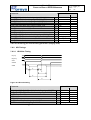
Figure 7: UART interface block diagram
3.2.1 UART Signals
The UART interface uses 2 data lines and 2 handshake lines.
Figure 8: UART signals
Signal
UART_TxD
UART_RxD
/UART_RTS
/UART_CTS
MCM connector pin
A17
A18
A19
A20
Table 4: UART connector pin assignments
UART_TxD
Transmit data output of the UART interface. For RS-232 usage, this signal must be connected to a
level converter. An example is shown in Figure 33.This signal is high when no data is transmitted.
USER’S GUIDE
PARALLEL BUS TO IEEE1394 BRIDGE
Date
: 25 October 2006
Doc. no. : Bridge_UG
Iss./Rev : 1.1
Page
: 26
UART_RxD
Receive data input of the UART interface. For RS-232 usage, this signal must be connected to a
level converter. An example is shown in Figure 33.This input must be high when idle.
/UART_RTS
Handshake output of the UART interface. For RS-232 usage, this signal must be connected to a
level converter. An example is shown in Figure 33. If RTS/CTS handshake is enabled (see chapter
3.2.2.2), a logic low level on this signal indicates that the UART interface can accept more data. If
RTS/CTS handshake is disabled, RTS is always active.
/UART_CTS
Handshake input of the UART interface. For RS-232 usage, this signal must be connected to a
level converter. An example is shown in Figure 33. If RTS/CTS handshake is enabled (see chapter
3.2.2.2), a logic low level on this input indicates that the MCM may transmit further data to the
connected hardware. If RTS/CTS handshake is disabled, this input is ignored.
3.2.2 UART Configuration
UART configuration can be divided into two sections: Parameters uart_baud and uart_handshake
configure the behavior of the UART interface itself. The remaining parameters deal with the virtual
connection. Table 5 lists the available configuration parameters.
Parameter name
uart_baud
uart_handshake
uart_connect
uart_partner_dev
uart_partner_inst
uart_tx_pktsize
uart_tx_timeout
uart_ev_bufsize
uart_rx_bufsize
uart_flowctl
uart_suspend
uart_resume
uart_rx_fifo_size
uart_tx_fifo_size
Meaning
baud rate configuration
enable/disable hardware handshake
connect UART interface of local device with partner node
partner node for virtual UART connection
partner instance (interface number) on the partner device
size of the event packets that are transmitted to the partner
maximum time in ms until pending data is sent
size of the buffer for incoming data events
number of data words that can be buffered by software
enable/disable virtual connection flow control
buffer fill level for suspending virtual connection transfer
buffer fill level for resuming virtual connection transfer
number of bytes that can be buffered in the receiver hardware
number of bytes that can be buffered in the transmitter hardware
Table 5: UART parameter overview
3.2.2.1 UART Baud Rate (uart_baud)
This parameter defines the baud rate of the UART interface. It can be set to
• 19200 baud
• 38400 baud
• 115200 baud
3.2.2.2 UART Handshake (uart_handshake)
This parameter controls the handshake type on the UART interface. It can be set to
• none (no handshake used)
• RTS / CTS handshake
Please refer to the signal description in chapter 3.2.1 to see how this parameter affects operation
of /UART_RTS and /UART_CTS.
USER’S GUIDE
PARALLEL BUS TO IEEE1394 BRIDGE
Date
: 25 October 2006
Doc. no. : Bridge_UG
Iss./Rev : 1.1
Page
: 27
3.2.2.3 UART Virtual Connection Control (uart_connect)
This parameter is used to establish a virtual connection of the local UART interface to a UART
interface on a remote device. If virtual connections are enabled, incoming UART data will be sent
over IEEE1394 to the configured partner device (see uart_partner_dev, uart_partner_inst). On the
partner device, this data will be output on its UART interface (if the partner device also has virtual
connections enabled). For receive direction, if virtual connections are enabled, UART character
events from the partner device will be transmitted on the local UART interface. The suggested
default setting for this parameter is to enable virtual connections.
3.2.2.4 UART Virtual Connection Control Partner Device(uart_partner_dev)
This parameter defines the partner device for virtual UART connections. It defines the device to
which the characters received on the UART interface are sent. Further, it defines, from which
device events are accepted (and therefore, from which device characters are transmitted on the
UART interface). Allowed values for this parameter are::
• The device ID of a remote device (0 .. 6210).
• "Broadcast / Accept any device" Incoming UART data will be sent to all devices in the
network via a IEEE1394 broadcast transaction. Incoming data (over IEEE1394) will be
accepted from all devices.
• "Use common partner device": the partner ID for the virtual UART connection will be taken
from the common parameter partner_dev ( see chapter 4.3.2).
The suggested default for this value is to use the common partner device.
3.2.2.5 UART Virtual Connection Partner Interface Instance (uart_partner_inst)
This parameter defines the interface instance (interface number) within the partner device for
virtual UART connections. This parameter is used for
• addressing the partner interface within the partner device (outgoing character events, flow
control events).
• filtering out the allowed partner for incoming character events
The instance of an interface is a simple number, starting at 0. The first UART interface of a device
has an instance of 0, the second of 1, etc.. Together with uart_partner_dev, this parameter defines
the virtual connection of this UART interface.
One special value is available for this parameter:
• "Accept any UART": The UART interface accepts character and flow control events from
any UART of the configured partner device and sends character and flow control events
using the local interface instance.
The suggested default for this value is 0, since typically there is only one UART interface per
device.
3.2.2.6 UART Transmit Packet Size (uart_tx_pktsize)
This parameters defines how many UART characters are transferred to the partner device in one
VCP character event. Allowed values are 1 to 2040 characters per event. Further, a special value
for this parameter exists: When uart_tx_pktsize is set to "variable packet size", as many characters
as possible are transferred (dynamic packet size).
The suggested default value for this parameter is "variable packet size" when another MCM is
used as partner device.
When a PC is used as partner device, uart_tx_pktsize should be set to its maximum value of 2040,
together with a timeout (see chapter 3.2.2.7). This limits the maximum event rate and is required
because flow control can't be used (due to the limited real-time behavior of Windows).
Alternatively, smaller packet sizes or less timeout can be used if a modified event FIFO setting on
the PC is used. Please refer to the description of the function VCP_EnableEventFifo() in [7].
USER’S GUIDE
PARALLEL BUS TO IEEE1394 BRIDGE
Date
: 25 October 2006
Doc. no. : Bridge_UG
Iss./Rev : 1.1
Page
: 28
3.2.2.7 UART Transmit Timeout (uart_tx_timeout)
This parameter works in conjunction with fixed transmit packet sizes greater than 1. If
uart_tx_pktsize is set to 0 (dynamic packet size) or 1, this parameter has no effect (see also
uart_tx_pktsize, chapter 3.2.2.6). uart_tx_timeout defines the maximum time in milliseconds for
waiting until a packet is complete. If this time expires, a character event is sent to the partner
device/interface using a smaller packet size than adjusted by uart_tx_pktsize. If no data at all is
present, no packet is sent. The timeout starts to expire with the first available data. When the
timeout is set to 0, the timeout feature is disabled and character events to the partner are only sent
if enough data is available. The maximum value for this parameter is 60,000 (1 minute). The
suggested default for this parameter is 100 ms for a PC as partner device and 0 (disabled) for a
MCM as partner device.
3.2.2.8 UART Virtual Connection Event Buffer Size (uart_ev_bufsize)
This parameter is read-only and is used for informational purposes only. It specifies the maximum
size in bytes for incoming character events. This information is useful for situations where the VCP
SDK is not available.
3.2.2.9 UART Virtual Connection Receive Buffer Size (uart_rx_bufsize)
This parameter is read-only and is used for informational purposes only. It specifies the number of
characters that can be buffered by software. This information is useful for situations where the VCP
SDK is not available.
3.2.2.10 UART Virtual Connection Flow Control (uart_rx_flowctl)
This parameter controls flow control for virtual UART connections. If enabled, the receiving device
sends a stop-event to the transmitting device, when the receive buffer gets filled over a specific
level (defined by uart_suspend). When the UART receive buffer fill level drops below a specific
level (defined by uart_resume), the receiving device sends a start-request to the transmitting
device to re-enable data transfer. In order to use this feature, the partner device must be real-time
capable so that it can disable transmission within a reasonable time.
The suggested default value for this parameter is to disable flow control when a PC is used as
partner and to enable flow control when another MCM is used as partner. Flow control is not
available with the VCP SDK due to the limited real-time behavior of Windows.
3.2.2.11 UART Buffer Fill Levels for Flow Control (uart_rx_suspend, uart_rx_resume)
These parameters define at which fill levels the receiver suspends and resumes transmission for a
virtual connection. uart_rx_suspend defines the fill level which generates a stop event for the
transmitting device, so that the transfer is suspended. uart_rx_resume defines the fill level which
generates a start event for the transmitting device, so that the transfer is resumed.
To use this feature, uart_rx_flowctl must be set to "enabled". The suggested default values are
uart_rx_bufsize – uart_tx_pktsize for uart_rx_suspend and uart_tx_pktsize for uart_rx_resume.
3.2.2.12 UART Hardware FIFO Sizes (uart_rx_fifo_size, uart_tx_fifo_size)
These parameters are read only. They define how many characters can be buffered by the UART
hardware and are used for informational purposes only.
3.3
Host Port Interface (HPI)
The host port interface is a 8 or 16 bit bi-directional parallel interface for easy connection to an
external host, such as a microcontroller. In contrast to the I/O pins or the UART interface, HPI data
transfers are always initiated by the (external) host. The HPI shares its signals with those of the I/O
pins. Depending on the HPI configuration, a different number of I/O pins are available (see chapter
3.4.1). Virtual HPI connections use either a fixed connection as defined by the configuration
parameters, or a dynamic addressing, where the host specifies the destination device. HPI data is
buffered by 16-word deep FIFOs in either direction.
USER’S GUIDE
PARALLEL BUS TO IEEE1394 BRIDGE
Date
: 25 October 2006
Doc. no. : Bridge_UG
Iss./Rev : 1.1
Page
: 29
Figure 9: HPI block diagram
3.3.1
HPI Signals
Figure 10: HPI signals3
HPI signal
Direction
Connector Available when HPI is
HD0
HD1
HD2
HD3
HD4
HD5
HD6
HD7
HD8_HA0
HD9
HD10
HD11
HD12
HD13
bi-directional
bi-directional
bi-directional
bi-directional
bi-directional
bi-directional
bi-directional
bi-directional
bi-directional
bi-directional
bi-directional
bi-directional
bi-directional
bi-directional
D6
D7
D8
D9
D10
D11
D12
D13
D14
D15
D16
D17
D19
D20
3
Alternative
function4
I/O0
I/O1
I/O2
I/O3
enabled
I/O4
I/O5
I/O6
I/O7
enabled and configured as 16 bit I/O85
I/O9
I/O10
I/O11
I/O12
I/O13
All signals shown; HD[15:8] only available in 16 bit mode, HA0 only available in 8 bit mode.
The alternative functions reside on a different connector! Please refer to the description of the I/O Pins.
5
I/O8 is used as HA0 in 8-bit mode and as HD8 in 16-bit mode.
4
USER’S GUIDE
PARALLEL BUS TO IEEE1394 BRIDGE
HPI signal
Direction
Connector Available when HPI is
HD14
HD15
/HCS
/HRD
/HWR
HD8_HA0
HA1
/HRRDY_HRDY
/HTRDY
bi-directional
bi-directional
input
input
input
input
input
output
output
D21
D22
D23
D24
D25
D14
D26
D27
C27
Date
: 25 October 2006
Doc. no. : Bridge_UG
Iss./Rev : 1.1
Page
: 30
Alternative
function4
I/O14
I/O15
I/O16
enabled
I/O17
I/O18
enabled and configured as 8 bit I/O85
enabled
I/O19
enabled with any handshake
I/O206
enabled
with
separate I/O217
handshake lines
Table 6: HPI connector pin assignments
HD[15:0]
HPI data bus. When the HPI is configured for 8-bit operation (hpi_width set to 8), HD[15:8] are not
available. The respective pins are used as HA0 and I/O[15:9].
Please note that the first data word is immediately available at HD[15:0]. A falling edge on /HRD
causes the current data to be placed on HD[15:0] as well as reading out the next data from the HPI
FIFO. However, the next data is transferred to HD[15:0] only after the next falling edge on /HRD.
/HCS
Active low chip select input. The host must activate this signal before it can perform a read or write
cycle.
/HRD
Active low read strobe. When /HCS is low, data is read out of the host port when /HRD is low.
Reading from an empty FIFO causes a FIFO underflow condition.
/HWR
Active low write strobe. When /HCS is low, data is written to the host port on a rising edge of
/HWR. Writing to a full FIFO causes a FIFO overflow condition.
HA[1:0]
These signals select which HPI register is accessed by the host (see chapter 3.3.3). HA0 is only
available when the host port is configured for 8-bit operation. Otherwise, this pin is used as HD8.
HA[1:0] must be stable during a HPI access.
/HRDY_/HRRDY
The function of this signal depends on HPI configuration parameter hpi_handshake. See chapter
3.3.2.3 for details. When hpi_handshake is set to "none", /HRDY_/HRRDY is not available and the
respective pin is used as I/O20.
When hpi_handshake is set to "separate handshake", this signal is used as a receive data
indicator (/HRRDY function) and can indicate two conditions:
• receive data available: at least one data word is available in the HPI FIFO to be read by the
host.
• error occurred: An error code is present in the HPI control register 2 an can be read by the
host
Additionally, if hpi_handshake is set to "common handshake", this signal is used as a host transfer
request indicator (/HRDY function) and can indicate the above described conditions plus
6
If HPI handshake is disabled, this pin can be used as general purpose output on BB26.
If HPI handshake is disabled or common handshake used, this pin can be used as general purpose output
on BB25.
7
USER’S GUIDE
PARALLEL BUS TO IEEE1394 BRIDGE
•
Date
: 25 October 2006
Doc. no. : Bridge_UG
Iss./Rev : 1.1
Page
: 31
transmit data request: The FIFO has one or more data words of free space that can be
written by the host.
The above listed conditions are only signaled if the respective bit in the HPIC1 register is enabled
by the host (see chapter 3.3.3.2, description of HPICA for details).
hpi_handshake
none
separate
common
HPIC1[7]
(ER_EN)
X
1
X
X
HPIC1[6]
(RRDY_EN)
HPIC[5]
(TRDY_EN)
/HRDY_/HRRDY function
X
X
X
1
I/O20
error indicator
receive data indicator
Transmit ready indicator
X
X
1
X
Table 7: Available functions for /HRDY_/HRRDY
/HRDY_/HRRDY is an active low output. When the above listed condition(s) are no longer true,
/HRDY_HRRDY is driven high for a short time and then left floating. This minimizes signal
contention when this signal is used as an interrupt output that is connected together with other
interrupt signals. See chapter 7.8.2 for details. When all signaling on this pin is disabled, this pin is
not driven (stays in high impedance).
/HTRDY
The function of this signal depends on HPI configuration parameter hpi_handshake. See chapter
3.3.2.3 for details. When hpi_handshake is set to "none" or "common handshake", /HTRDY is not
available and the respective pin is used as I/O21.
When hpi_handshake is set to "separate handshake", this signal is used as a host transfer request
indicator and can indicate the following condition:
• Transmit data request: The FIFO has one or more data words of free space that can be
written by the host.
This condition is only signaled if the respective bit in the HPIC1 register (Bit 5, TRDY_EN) is
enabled by the host (see chapter 3.3.3.2 for details).
/HTRDY is an active low output. When the above listed condition is no longer true, /HTRDY is
driven high for a short time and then left floating. This minimizes signal contention when this signal
is used as an interrupt output that is connected together with other interrupt signals. See chapter
7.8.2 for details. When signaling on this pin is disabled, this pin is not driven (stays in high
impedance).
3.3.2 HPI Configuration
From a hardware point of view the HPI can be configured to use 8 or 16 data bits (hpi_width) and
one to of three handshake types (hpi_handshake):
• none
• common handshake signal (/HRDY)
• separate handshake signals for each direction (/HRRDY, /HTRDY)
Further, the HPI can be totally disabled (parameter hpi_en).
Other parameters of the HPI configure virtual connection operation.
Table 8 lists all available configuration parameters.
USER’S GUIDE
PARALLEL BUS TO IEEE1394 BRIDGE
Parameter name
hpi_en
hpi_width
hpi_handshake
hpi_connect
hpi_partner_dev
hpi_partner_inst
hpi_tx_pktsize
hpi_tx_timeout
hpi_ev_bufsize
hpi_rx_bufsize
hpi_flowctl
hpi_suspend
hpi_resume
hpi_rx_fifo_size
hpi_tx_fifo_size
Date
: 25 October 2006
Doc. no. : Bridge_UG
Iss./Rev : 1.1
Page
: 32
Meaning
switches between I/O pin and HPI usage
number of bits
handshake type signals
connect HPI of local device with partner node
partner node for virtual HPI connection
partner instance (interface number) on the partner device
size of the event packets that are transmitted to the partner
maximum time in ms until pending data is sent
size of the buffer for incoming data events
size of the software buffer for incoming HPI data
enable/disable virtual connection flow control
used for HPI flow control
used for HPI flow control
number of data words that can be buffered in the HPI
number of data words that can be buffered in the HPI
Table 8: HPI parameter overview
3.3.2.1 HPI Enable (hpi_en)
This parameter enables the HPI. It has two possible values
• enabled (shared pins are used as host port interface)
• disabled (shared pins are used as I/O pins)
3.3.2.2 HPI Bus Width (hpi_width)
This parameter controls, whether the HPI is an 8 bit or a 16 bit interface. In 8-bit mode, data
transfers use only 8 data bits (HD[7:0]), the HPI registers are split into two 8 bit registers and HPI
addressing uses an additional address line (HA0).
3.3.2.3 HPI Handshake Type (hpi_handshake)
This parameter defines how the signals /HRRDY_HRDY and /HTRDY are used. Possible settings
are
• No handshake: /HRRDY_HRDY and /HTRDY are used as general purpose I/O pins (I/O
pins 20 and 21).
• Common handshake: /HRRDY_/HRDY is used as common handshake line (/HRDY
function selected), /HTRDY is used as general purpose I/O (I/O pin 21).
• Separate handshake: /HRRDY_/HRDY is used as receive ready (/HRRDY function
selected), /HTRDY is used as transmit ready.
3.3.2.4 HPI Virtual Connection Control (hpi_connect)
This parameter is used to establish a virtual connection of the local HPI to a HPI interface on a
remote device. If virtual connections are enabled, incoming HPI data from the host will be sent over
IEEE1394 to the configured partner device (see hpi_partner_dev, hpi_partner_inst). On the partner
device, this data will be output on its HPI interface (if the partner device also has virtual
connections enabled). In receive direction, if virtual connections are enabled, HPI data events from
the partner device will be transmitted to the local HPI interface. The suggested default setting for
this parameter is to enable virtual connections.
3.3.2.5 HPI Virtual Connection Partner Device (hpi_partner_dev)
This parameter defines the partner device for virtual HPI connections. It defines the device to
which the data received from the host is sent. Further, it defines, from device data and flow control
events are accepted. Allowed values for this parameter are:
USER’S GUIDE
PARALLEL BUS TO IEEE1394 BRIDGE
Date
: 25 October 2006
Doc. no. : Bridge_UG
Iss./Rev : 1.1
Page
: 33
•
•
The device ID of a remote device (0 .. 6210).
"Accept any device": Incoming data will be sent to all devices in the network via a
IEEE1394 broadcast transaction. Incoming data (from IEEE1394) will be accepted from all
devices.
• "Use common partner device": the partner ID for the virtual HPI connection will be taken
from the common parameter partner_dev ( see chapter 4.3.2).
• "Use dynamic addressing": The host defines the partner device for outgoing HPI data
events. See description of the ID bit field in chapter 3.3.3.2 for details.
The suggested default for this value is to use the common partner device.
3.3.2.6 HPI Virtual Connection Partner Interface Instance (hpi_partner_inst)
This parameter defines the interface instance (interface number) within the partner device for
virtual HPI connections. This parameter is used for
• addressing the partner interface within the partner device (outgoing data events, flow
control events).
• filtering out the allowed partner for incoming events
The instance of an interface is a simple number, starting at 0. The first HPI interface of a device
has an instance of 0, the second of 1, etc.. Together with hpi_partner_dev, this parameter defines
the virtual connection of this HPI.
One special value is available for this parameter:
• "Accept any HPI": The HPI interface accepts data and flow control events from any HPI of
the configured partner device and sends data and flow control events using the local
interface instance.
The suggested default for this value is 0, since typically there is only one HPI per device.
3.3.2.7 HPI Transmit Packet Size (hpi_tx_pktsize)
This parameters defines how many bytes are transferred to the partner device in one data event.
Allowed value range for this parameter is 1 to 2040, however, when the HPI is operated in 16-bit
configuration (hpi_width = 16), only multiples of 2 should be used. A special value for this
parameter also exists: When hpi_tx_pktsize is set to "variable packet size", as many characters as
possible are transferred (dynamic packet size).
The suggested default value for this parameter is "variable packet size" when another MCM is
used as partner device.
When a PC is used as partner device, hpi_tx_pktsize should be set to its maximum value of 2040,
together with a timeout (see chapter 3.3.2.8). This limits the maximum event rate and is required
because flow control can't be used (due to the limited real-time behavior of Windows).
Alternatively, smaller packet sizes or less timeout can be used if a modified event FIFO setting on
the PC is used. Please refer to the description of the function VCP_EnableEventFifo() in [7].
3.3.2.8 HPI Transmit Timeout (hpi_tx_timeout)
This parameter works in conjunction with fixed transmit packet sizes greater than 1. If
hpi_tx_pktsize is set to 0 (dynamic packet size) or 1, this parameter has no effect (see also
hpi_tx_pktsize, chapter 3.3.2.7). hpi_tx_timeout defines the maximum time in milliseconds for
waiting until a packet is complete. If this time expires, a data event is sent to the partner
device/interface using a smaller packet size than adjusted by hpi_tx_pktsize. If no data at all is
present, no packet is sent. The timeout starts to expire with the first available data. When the
timeout is set to 0, the timeout feature is disabled and character events to the partner are only sent
if enough data is available. The maximum value for this parameter is 60,000 (1 minute). The
suggested default for this parameter is 100 ms for a PC as partner device and 0 (disabled) for a
MCM as partner device.
USER’S GUIDE
PARALLEL BUS TO IEEE1394 BRIDGE
Date
: 25 October 2006
Doc. no. : Bridge_UG
Iss./Rev : 1.1
Page
: 34
3.3.2.9 HPI Virtual Connection Event Buffer Size (hpi_ev_buffer_size)
This parameter is read-only and is used for informational purposes only. It specifies the maximum
size in bytes for incoming data events. This information is useful for situations where the VCP SDK
is not available.
3.3.2.10 HPI Virtual Connection Receive Buffer Size (hpi_rx_bufsize)
This parameter is read-only and is used for informational purposes only. It specifies the number of
bytes that can be buffered by software. This information is useful for situations where the VCP
SDK is not available.
3.3.2.11 HPI Virtual Connection Flow Control (hpi_flowctl)
This parameter controls flow control for virtual HPI connections. If enabled, the receiving device
sends a stop-event to the transmitting device, when the receive buffer gets filled over a specific
level (defined by hpi_suspend). When the HPI receive buffer fill level drops below a specific level
(defined by hpi_resume), the receiving device sends a start-request to the transmitting device to
re-enable data transfer. In order to use this feature, the partner device must be real-time capable
so that it can disable transmission within a reasonable time.
The suggested default value for this parameter is to disable flow control when a PC is used as
partner and to enable flow control when another MCM is used as partner. Flow control is not
available with the VCP SDK due to the limited real-time behavior of Windows.
3.3.2.12 HPI Buffer Fill Levels for Flow Control (hpi_rx_suspend, hpi_rx_resume)
These parameters define at which fill levels the receiver suspends and resumes transmission for a
virtual connection. hpi_rx_suspend defines the fill level (in bytes) which generates a stop event for
the transmitting device, so that the transfer is suspended. hpi_rx_resume defines the fill level (in
bytes) which generates a start event for the transmitting device, so that the transfer is resumed.
To use this feature, hpi_rx_flowctl must be set to "enabled". The suggested default values are
hpi_rx_bufsize – hpi_tx_pktsize for hpi_rx_suspend and hpi_tx_pktsize for hpi_rx_resume.
3.3.2.13 HPI Hardware FIFO Sizes (hpi_rx_fifo_size, hpi_tx_fifo_size)
These parameters are read only. They define how many data words can be buffered by the HPI
hardware and are used for informational purposes only.
3.3.3 HPI Registers (Host Side)
An external host has access to one HPI data register (HPID) and two HPI control registers (HPIC1,
HPIC2). In 8-bit configuration, the HPI registers are split into two 8-bit halves and HA0 switches
between these register halves. Addressing of the two HPI control registers is done by the HPICA
bit which is present in both HPIC registers.
HPICA
0
0
1
1
HA1
0
1
0
1
HA0
0
0
0
0
Register
HPID
HPIC1
n/a
HPIC2
Table 9: HPI address map in 16-bit configuration
Date
: 25 October 2006
Doc. no. : Bridge_UG
Iss./Rev : 1.1
Page
: 35
USER’S GUIDE
PARALLEL BUS TO IEEE1394 BRIDGE
HPICA
0
0
0
0
1
1
1
1
HA1
0
0
1
1
0
0
1
1
HA0
0
1
0
1
0
1
0
1
Register
HPID[7:0]
reserved
HPIC1[7:0]
HPIC1[15:8]
n/a
n/a
HPIC2[7:0]
HPIC2[15:8]
Table 10: HPI address map in 8-bit configuration
The layout of the HPI registers is shown in Table 11 and Table 12.
Bit
HPID
HPIC1
HPIC2
15
14
13
HPICA RSV
HPICA
8
DST_ID
7
6
5
HPI_DATA
ERR_EN RRDY_EN TRDY_EN
RESERVED
4
3
2
UN
OV
ERRCLR
TEMPTY
1
0
RRDY TRDY
ERR
Table 11: HPI register layout in 16-bit configuration
Bit
HPID[7:0]
HPIC1[7:0]
HPIC1[15:8]
HPIC2[7:0]
HPIC2[15:8]
7
6
5
4
3
2
1
HPI_DATA[7:0]
ERR_EN RRDY_EN TRDY_EN
UN
OV
TEMPTY RRDY
HPICA
RSV
DST_ID
RESERVED
ERRCLR
ERR
HPICA
RSV
0
TRDY
Table 12: HPI register layout in 8-bit configuration
3.3.3.1 HPI Data Register
The HPI data register allows to access the HPI FIFOs. Any read of the HPI data register reads out
one 8-bit or one 16-bit word from the HPI FIFO. A read from an empty FIFO yields the last read
value. Writes to HPID transfer one data word (8 bit or 16 bit) the HPI FIFO. Writes to a full FIFO
are ignored, so that the FIFO contents isn't changed. When using dynamic addressing
(hpi_partner_dev set to dynamic addressing), the HPI data register works in conjunction with the ID
bit field in HPIC1.
3.3.3.2 HPI Control Register 1 (HPIC1)
This register is used to control communication between host and the MCM. The host accesses this
register for:
• determining the state of the HPI FIFOs (TRDY, RRDY, TEMPTY, OV, UN)
• control handshake or error signaling over dedicated HPI signals (TRDY_EN, RRDY_EN,
ERR_EN)
• control the destination ID for outgoing data if dynamic addressing is selected
(hpi_partner_dev = "use dynamic addressing")
• retrieve the source of incoming HPI data if dynamic addressing is selected
(hpi_partner_dev = "use dynamic addressing")
• switch to HPIC2 (by setting HPICA)
15
14
HPICA RSV
r,w,0
r,0
13
8
ID
(r),(w),000000
7
6
5
4
ERR_EN RRDY_EN TRDY_EN UN
r,w,0
r,w,0
r,w,0
r,wc,0
3
2
1
0
OV TEMPTY RRDY TRDY
r,wc,0
r,1
r,0
r,1
USER’S GUIDE
PARALLEL BUS TO IEEE1394 BRIDGE
Date
: 25 October 2006
Doc. no. : Bridge_UG
Iss./Rev : 1.1
Page
: 36
TRDY
This bit indicates that the HPI FIFO can accept at least two more data words from the host (TRDY
= 1). TRDY is inactive when there is space for less than two data words in the FIFO. TRDY is readonly. The host should check the TRDY bit before writing to the HPID register.
RRDY
This bit indicates that the HPI FIFO has at least one more data word to be read by the host (RRDY
= 1). RRDY goes inactive after the host has read the last data from the HPI and no new data has
arrived at the HPI. RRDY is read-only. The host should check RRDY before reading the HPID
register.
TEMPTY
This bit indicates that all data from the host has been processed by the UC1394a-1. The host can
use this bit to initiate a block write to the HPI data register. When TEMPTY is active (1), as many
data words as defined by hpi_tx_fifosize can be written to the HPID register without checking for
the TRDY bit.
OV
This bit indicates that the host has written to the HPID register while the HPI FIFO was full.
Therefore, OV indicates that data got lost. The host can clear the OV bit by writing a '1' to it. The
host should check the OV bit periodically to detect handshaking errors.
UN
This bit indicates that the host has read from the HPID register while the RRDY was inactive.
Therefore, UN indicates that invalid data was read from HPID. The host can clear the UN bit by
writing a '1' to it. The host should check the UN bit periodically to detect handshaking errors.
TRDY_EN
This bit controls whether the "transmitter ready" condition is signaled on one of the HPI handshake
signals. Please note that configuration parameter hpi_handshake controls the behavior of the
handshake signals:
•
•
•
hpi_handshake set to "separate handshake": TRDY output on /HTRDY
hpi_handshake set to "common handshake": TRDY output on /HRRDY_HTRDY, together
with the RRDY condition
hpi_handshake set to "no handshake": no TRDY signaling
To enable "transmitter ready" signaling, the host must set the TRDY_EN bit. Then, /HTRDY or
/HRRDY_HTRDY is active (low) when the HPID register can accept at least two more data words.
RRDY_EN
This bit controls whether the "receiver ready" condition is signaled on /HRDY_HRRDY. Please
note that
• the /HRDY_HRRDY pin is disabled when hpi_handshake is set to "no handshake"
• the /HRDY_HRRDY pin is shared with the '"transmitter ready" condition when
hpi_handshake is set to "common handshake" and with error signaling when ERR_EN is
set to 1 (see description or ERR_EN for details).
To enable "receiver ready" signaling, the host must set the RRDY_EN bit. Then, /HRDY_HRRDY
is active (low) when the HPID register holds valid data.
ERR_EN
This bit controls whether error conditions are signaled over the HPI signal /HRDY_HRRDY. Please
note that this signaling is disabled, when the configuration parameter hpi_handshake is set to "no
USER’S GUIDE
PARALLEL BUS TO IEEE1394 BRIDGE
Date
: 25 October 2006
Doc. no. : Bridge_UG
Iss./Rev : 1.1
Page
: 37
handshake". The host must set ERR_EN to enable error signaling. When error signaling is
enabled, /HRDY_HRRDY will get active (low) whenever an error occurs. The host can enable this
feature to get informed about errors. Alternatively, the host can poll the ERRDTCT bit in the HPIC2
register. Please note that the /HRDY_HRRDY signal can be shared with the receiver ready
condition (see description of RRDY_EN) and the transmitter ready condition (see description of
TRDY_EN).
ID
This bit field has a different meaning for each access direction:
• When reading HPIC1, ID holds the device ID of that device that supplied the current data in
the HPID register. The ID bit field is updated when the associated data is read. Therefore,
the ID must be read before the data is read. The ID field is used when both, the partner
device and the local device are configured for dynamic addressing by configuration
parameter hpi_partner_dev.
• When writing to HPIC1, ID determines the destination ID for the next data that is written to
HPID. When the configuration parameter hpi_partner_dev is set to "dynamic addressing",
this ID will be used to address the partner device for this data. The host must set this bit
field to the ID of the device that should receive the next data before the data itself is written
to the HPID register. ID needs to be set only when the destination ID changes. Subsequent
writes to HPID will use the same ID.
The ID bit field is FIFO-buffered, such as the HPI data register (HPID), for both directions.
HPICA
This bit is the HPIC address bit. If set to 0, HPIC1 is selected and the remaining bits of this register
behave as described above. When HPICA is set to 1, HPIC2 is selected and the remaining bits
behave as described in the following chapter. The host uses HPICA to switch between HPIC1 and
HPIC2. The HPICA bit is present in both registers, so that it is always accessible, independent of
which register is selected. When writing to HPIC1, the HPICA bit is modified after the access.
Therefore, the current write access is not affected by a change of the HPICA bit.
Code example:
#define HPID (HPI_BASE_ADDRESS + 0) /* HPI data register */
#define HPIC1 (HPI_BASE_ADDRESS + 1) /* HPI control register 1 */
#define HPIC2 (HPI_BASE_ADDRESS + 1) /* HPI control register 2 */
#define HPIC3 (HPI_BASE_ADDRESS + 2) /* HPI control register 3 (carrier board) */
/* HPI register bit definitions */
#define HPICX_HPICA
0x8000 /* HPICA bit */
#define HPICX_HPIC1
0x0000 /* HPICA setting for HPIC1 (HPICA is present in HPIC1 and HPIC2) */
#define HPICX_HPIC2
0x8000 /* HPICA setting for HPIC2 (HPICA is present in HPIC1 and HPIC2) */
#define HPIC1_RRDY_EN 0x0040 /* Receiver ready handshake enable */
#define HPIC2_ERRDTCT 0x0008 /* error detect / error acknowledge */
#define HPI_READ(reg)
(*(volatile unsigned int *)reg)
#define HPI_WRITE(reg, val) (*(volatile unsigned int *)reg) = val;
/* get currently addressed HPIC register */
unsigned int uiReg = HPI_READ(HPIC1);
/* if current state of HPICA is not known, use this to determine which register is selected */
if (uiReg & HPICX_HPICA) == HPICX_HPIC2)
{
/* ERRDTCT is cleared by setting it, so clear this bit to leave it untouched */
uiReg&= ~HPIC2_ERRDTCT;
/* clear HPICA bit */
uiReg&= ~HPICX_HPICA;
/* switch to HPIC1 */
HPI_REG(HPIC2) = ulReg;
}
#if 0 /* slow, but more readable version */
/* get HPIC1 */
uiReg = HPI_READ(HPIC1);
/* enable RRDY handshake in HPIC1 (and stay in HPIC1)*/
uiReg|= HPIC1_RRDY_EN;
HPI_WRITE(HPIC1, ulReg);
/* switch to HPIC2 (set HPICA bit) */
uiReg|= HPICX_HPIC2;
HPI_WRITE(HPIC1, ulReg);
#else /* fast version */
/* enable RRDY handshake in HPIC1 and switch to HPIC2)*/
uiReg|= HPIC1_RRDY_EN | HPICX_HPIC2;
HPI_WRITE(HPIC1, ulReg);
Date
: 25 October 2006
Doc. no. : Bridge_UG
Iss./Rev : 1.1
Page
: 38
USER’S GUIDE
PARALLEL BUS TO IEEE1394 BRIDGE
#endif
/* clear ERRDTCT in HPIC2 (acknowledge the last error) */
uiReg = HPI_READ(HPIC2);
uiReg|= HPIC2_ERRCLR;
HPI_WRITE(uiReg);
3.3.3.3 HPI Control Register 2 (HPIC2)
This register is used for diagnostic purposes. It provides an alternative access to the 3-bit error
code (see Table 16). The host uses this register to
•
•
•
check for errors
determine the error type
acknowledge an error
See also chapter 3.5 for using the diagnostic interface.
15
14
13
12
11
10
9
8
7
6
5
4
3
2
1
HPICA
RESERVED
ERRDTCT
ERR
r,w,0
r,00000000000
r,wc,0
r,000
0
ERR
This bit field contains the current error code as defined by Table 16.
ERRDTCT
This bit indicates that an error is present and ERR[2:0] define the type of the error. The host can
read this bit to check if an error has occurred (ERRDTCT = 1). When an error has occurred, the
host should examine ERR[2:0] for the cause of the error and then take the appropriate action. After
that, the host should acknowledge the error by writing a '1' to the ERRDTCT bit. The UC1394a-1
immediately clears ERRDTCT. If more errors are present, the next error code is read from the error
FIFO, the error code is written to ERR[2:0] and ERRDTCT is set again. Please note that this error
interface is connected to the same error FIFO as the hardware diagnostic interface. When an error
is acknowledged on either interface, the next error code is written to both interfaces. Therefore,
only one of both interfaces (diagnostic interface over dedicated I/O pins (chapter 3.5.2) or HPI)
should be used.
Code example:
/* HPI registers address map */
#define HPID (HPI_BASE_ADDRESS + 0) /* HPI data register */
#define HPIC1 (HPI_BASE_ADDRESS + 1) /* HPI control register 1 */
#define HPIC2 (HPI_BASE_ADDRESS + 1) /* HPI control register 2 */
#define HPIC3 (HPI_BASE_ADDRESS + 2) /* HPI control register 3 (carrier board) */
/* HPI register bit definitions */
#define HPICX_HPIC1
0x0000 /* HPICA setting for HPIC1 (HPICA is present in HPIC1 and HPIC2) */
#define HPICX_HPIC2
0x8000 /* HPICA setting for HPIC2 (HPICA is present in HPIC1 and HPIC2) */
#define HPIC2_ERRDTCT 0x0008 /* error detedct / error acknowledge */
#define HPIC2_ERR_MASK 0x0007 /* error detedct / error acknowledge */
#define HPI_REG(reg) (*(volatile unsigned int *)reg)
/* get current HPIC configuration and switch to HPIC2 if HPIC1 is currently selected */
prev_hpic = HPI_REG(HPIC1);
if ((prev_hpic & HPICX_HPIC2) == 0)
HPI_REG(HPIC2) = HPICX_HPIC2;
/* check for errors */
if HPI_REG(reg) (*(volatile unsigned int *)reg)
{
/* get the error code */
error = HPI_REG(HPIC2) & HPIC2_ERR_MASK;
/* error handling */
...
/* acknowledge error */
HPI_REG(HPIC2) = HPIC2_ERRDTCT;
}
/* switch back to HPIC1 if neccessary */
if ((prev_hpic & HPICX_HPIC2) == 0)
HPI_REG(HPIC2) = prev_hpic;
USER’S GUIDE
PARALLEL BUS TO IEEE1394 BRIDGE
Date
: 25 October 2006
Doc. no. : Bridge_UG
Iss./Rev : 1.1
Page
: 39
HPICA
This bit is the HPIC address bit. If set to 0, HPIC1 is selected and the remaining bits of this register
behave as described in chapter 3.3.3.2. When HPICA is set to 1, HPIC2 is selected and the
remaining bits of this register behave as described above in this chapter. The host uses HPICA to
switch between HPIC1 and HPIC2. The HPICA bit is present in both registers, so that it is always
accessible, independent of which register is selected. For further details please refer to the
description of HPICA in chapter 3.3.3.2.
3.3.3.4 HPI Control Register 3 (HPIC3)
The HPIC3 register is implemented on the carrier board and therefore neither available nor
necessary on the MCM.
3.4
I/O Pins
The UC1394a-1 MCM has up to 27 general purpose I/O pins.
Figure 11: I/O pin block diagram
Each I/O pin can be individually configured to be an
• input
• push-pull output
• open drain output
USER’S GUIDE
PARALLEL BUS TO IEEE1394 BRIDGE
Date
: 25 October 2006
Doc. no. : Bridge_UG
Iss./Rev : 1.1
Page
: 40
Figure 12: I/O pin configurations
The VCP allows connection between any two I/O pins on any two devices. When two I/O pins are
virtually connected, one pin must be output and one must be input. State changes on the input pin
generate an event that is sent to the output pin. Polling the current state of an I/O pin is also
supported by the VCP.
Figure 13: Example for a virtual connection between two I/O pins
On the UC1394a-1 MCM, the I/O pins are shared with the HPI and the diagnostic interface, so their
presence depends on the configuration of these interfaces. See chapters 3.3.1, 3.3.2.1 through
3.3.2.3 and 3.5.2 for details.
Some of the I/O pins are sampled at system startup. Their startup state defines a part of the
UC1394a-1 MCM configuration as shown in Figure 11.
USER’S GUIDE
PARALLEL BUS TO IEEE1394 BRIDGE
3.4.1
Date
: 25 October 2006
Doc. no. : Bridge_UG
Iss./Rev : 1.1
Page
: 41
I/O Pin Signals
I/O Pin MCM connector pin Startup state Alternative functions8
defines
HPI 8-bit
HPI 16-bit
0
D6
HD0
HD0
1
D7
HD1
HD1
2
D8
HD2
HD2
3
D9
HD3
HD3
4
D10
HD4
HD4
5
D11
HD5
HD5
6
D12
HD6
HD6
7
D13
HD7
HD7
8
D14
HA0
HD8
9
D15
HD9
10
D16
HD10
11
D17
HD11
12
D19
HD12
13
D20
HD13
14
D21
HD14
15
D22
HD15
16
D23
/HCS
/HCS
device ID9
17
D24
/HRD
/HRD
18
D25
/HWR
/HWR
partner ID10
19
D26
HA1
HA1
20
D27
/HRRDY /HRDY /HRRDY /HRDY
21
C27
/HTRDY
/HTRDY
22
A12
configuration
mode
23
A13
24
A14
25
A15
26
A16
streaming11
direction
Diagnostics
/ERRDTCT
/ERRCLR
ERR0
ERR1
ERR2
Table 13: I/O pin assignments
3.4.2 I/O Pin Alternative Functions
If the host port is enabled (configuration parameter hpi_enable), I/O[8:0] and I/O[21:16] are
disabled, independent of the HPI configuration. The availability of /O [15:9] depends on the HPI
configuration (parameter hpi_width): In 8-bit mode, I/O[15:9] are still available, whereas in 16-bit
mode I/O[15:9] are also disabled.
A similar situation exists for the usage of IO[26:22]: If the diagnostic interface is enabled
(parameter diag_iftype set to "Error signal only" or "Error code output"), I/O[23:22] are always used
for diagnostics and are no longer available as I/O pins. Further, if the diagnostic interface is
configured for error code output (diag_iftype set to "Error code output"), I/O[26:24] are also used
for diagnostics.
8
If one of the alternative functions is enabled, the respective I/O pin is no longer available
Only used if dev_id is set to "read from I/O pin"
10
Only used if partner_dev is set to "read from I/O pin"
11
Only used if str_dir is set to "read from I/O26"
9
USER’S GUIDE
PARALLEL BUS TO IEEE1394 BRIDGE
Date
: 25 October 2006
Doc. no. : Bridge_UG
Iss./Rev : 1.1
Page
: 42
3.4.3 I/O Pin Startup State Options
Some of the I/O Pins are sampled at system startup. Their state can be used to configure
operation of the MCM. After system startup, the I/O pins can be used for other purposes. In order
to avoid conflicts with later usage, the startup state should be defined by pull-up/pull-down resistors
or by a driver that is disabled after system startup (see wiring examples in chapters 6.3 and 6.4.
3.4.3.1 Setting the Device ID over I/O Pins
This feature is useful if the end-user must be able to change the device ID, e.g. when the end-user
builds a system that consists of several MCMs. When using this option, the device ID is restricted
to values of 0 .. 7. To use this option, configuration parameter dev_id must be set to "read from I/O
pin". Please note that this feature is still available even when the HPI is used instead of the I/O
pins, since the I/O pins are sampled before the HPI is enabled. The device ID is encoded as
follows:
Pin
I/O16
I/O17
I/O18
-
Function
device ID Bit 0
device ID Bit 1
device ID Bit 2
(device ID Bit 3..5 are set to 0)
3.4.3.2 Setting the Partner Device ID over I/O Pins
This feature is useful if the end-user must be able to change the partner ID, e.g. when the end-user
builds a pure embedded system that consists of several MCMs. When using this option, the
partner ID is restricted to values of 0 .. 7. To use this option, configuration parameter partner_dev
must be set to "read from I/O pin". Please note that this feature is still available even when the HPI
is used instead of the I/O pins, since the I/O pins are sampled before the HPI is enabled. The
partner device ID is encoded as follows:
Pin
I/O19
I/O20
I/O21
-
Function
partner device ID Bit 0
partner device ID Bit 1
partner device ID Bit 2
(partner device ID Bit 3..5 are set to 0)
3.4.3.3 Setting the Configuration Mode over I/O Pins
The configuration mode is a basic setting that is always used, independent of the configuration.
Therefore, setting up the configuration mode must be done in any implementation. See also
chapter 6.3 for wiring examples. The available configuration modes are described in chapter 4.1.
The configuration mode is read from I/O[25:22] as follows:
Pin
I/O22
I/O23
I/O24
I/O25
Function
configuration mode Bit 0
configuration mode Bit 1
configuration mode Bit 2
configuration mode Bit 3
3.4.3.4 Setting the Streaming Direction over I/O Pins
This feature is used by the bridging kit [1] to allow quick start examples without configuration
required.
It can also used for systems where the streaming direction is not known during production, but later
on at system startup. A jumper or some programmable logic can define the startup state of I/O26 to
define the direction of str4eaming transfers. To use this feature, configuration parameter str_dir
USER’S GUIDE
PARALLEL BUS TO IEEE1394 BRIDGE
Date
: 25 October 2006
Doc. no. : Bridge_UG
Iss./Rev : 1.1
Page
: 43
must be set to "read from I/O pin". Please note: For applications that require to change streaming
direction during runtime, the method described in chapter 3.1.3.3 is preferred. The streaming
direction is encoded as follows:
Startup state of I/O26
high
low
Streaming direction
transmit
receive
3.4.4 I/O Pin Configuration
I/O pin configuration can be divided into two sections: Parameters io_dir and io_otype are used to
configure the behavior of the physical pin. The remaining parameters deal with the virtual
connection. Table 14 lists the available configuration parameters.
Parameter name
io_dir
io_otype
io_state
io_connect
io_partner_dev
io_partner_inst
io_enable
Meaning
pin direction
output type (applies only if configured as output)
default state after startup (applies only if configured as output)
enables virtual connection to partner pin
partner device for this I/O pin
partner instance (partner pin) on the partner device associated with this pin
tells if the I/O pin is available or used by an alternative interface
Table 14: I/O pin parameter overview
3.4.4.1 I/O Pin Direction (io_dir)
This parameter determines, whether the associated I/O pin is an input or an output.
3.4.4.2 I/O Pin Output Type (io_otype)
This parameter affects I/O pin behavior when it is configured as an output. It can be set to
•
•
Push-pull output.
Open-drain output.
Figure 12 illustrates the output types. Selecting a push-pull output causes the output to be pulled
low or high by low impedance, according to the state of the I/O pin. An open drain output pulls
down the I/O pin with low impedance when the state is low (logic 0). When the state is set high
(logic 1), the I/O pin is pulled high with high impedance (pull-up resistor). Using open-drain outputs
allows to connect several outputs together without signal contention. On the other hand, a push–
pull output allows more switching speed and faster low to high transitions, especially at high
capacitive loads.
3.4.4.3 I/O Pin Startup Output State (io_state)
This parameter selects the startup state of an I/O pin when it is configured as an output. This state
is overwritten by the first incoming VCP event from the partner pin. Allowed values for this
parameter are
• low (pulled to 0 V)
• high (pulled to 3.3 V)
3.4.4.4 I/O Pin Virtual Connection Control (io_connect)
This parameter defines, if an I/O pin generates pin state events (configured as input) or whether
the I/O pin accepts incoming pin state events (configured as output). The suggested default for this
parameter is to enable the virtual connection.
USER’S GUIDE
PARALLEL BUS TO IEEE1394 BRIDGE
Date
: 25 October 2006
Doc. no. : Bridge_UG
Iss./Rev : 1.1
Page
: 44
3.4.4.5 I/O Pin Partner Device for Virtual Connections (io_partner_dev)
This parameter defines the partner device for this I/O pin. Together with io_partner_inst, this
parameter defines the virtual connection of this pin. Allowed values for this parameter are:
• The device ID of a remote device (0 .. 6210).
• "Accept any device": The I/O pin accepts pin state events from any device (configured as
input) and sends pin state events as broadcasts (configured as output).
• "Use common partner ID": The partner device ID is taken from the device parameter
partner_dev (see chapter 4.3.2).
The suggested default for this parameter is to use the common partner ID.
3.4.4.6 I/O Pin Partner Pin for Virtual Connections (io_partner_inst)
This parameter defines the interface instance that is used as partner for this I/O pin. The interface
instance is the number of the I/O pin. For example, I/O pin 0 has an interface instance of 0, etc..
Together with io_partner_dev, this parameter defines the virtual connection of this pin.
One special value is available for this parameter:
• "Accept any Pin": The I/O pin accepts pin state events from any I/O pin of the configured
partner device (if configured as output) or sends pin state events to the same I/O pin (if
configured as input).
The suggested default for this parameter is to set it to the own pin number, thus io_partner_inst of
I/O0 is set to, io_partner_inst of I/O1 is set to 1 and so on.
3.4.4.7 I/O Pin Presence Control (io_enable)
This parameter is not writeable. Instead, it is controlled by the alternative functions of the I/O pin.
For example, if the HPI is enabled, I/O pin 0 is no longer available and io_enable of I/O0 is set to
"disabled".
3.5
Diagnostic Interface
The diagnostic interface stores every error or abnormal condition in two error FIFOs. One error
FIFO contains detailed information about an abnormal condition, including the interface that the
error is related to and a timestamp when the error happened. This FIFO is connected to the
IEEE1394 interface for diagnosis at a central point in the IEEE1394 network.
The other error FIFO contains an error code that is forwarded to the following interfaces
•
•
•
UC1394a-1 MCM LED (output as a blink code)
dedicated I/O pins
HPI
This error FIFO can be used by local hardware for error handling and simple error statistics, e.g.
counting the errors.
USER’S GUIDE
PARALLEL BUS TO IEEE1394 BRIDGE
Date
: 25 October 2006
Doc. no. : Bridge_UG
Iss./Rev : 1.1
Page
: 45
Figure 14: Diagnostic interface block diagram
3.5.1 Diagnostic Interface over IEEE1394
When an abnormal condition occurs, it is stored in the detailed error FIFO. If the FIFO is full,
further errors won't be written to the FIFO. This ensures that the FIFO contains the very first error
and not subsequent errors that resulted from the first errors. Optionally, an error notification event
can be sent to a remote device.
The error FIFO can be read out by any remote device. The user has to ensure, that only one
device reads diagnostic information. Details about the diagnostic FIFO can be found in [3]. The
detailed error codes, supported by the detailed error FIFO are listed in Table 17.
The error FIFO can also be completely cleared by a diagnostic host. This allows to restart error
statistics after an error condition has been removed, without resetting the whole system. This clear
command not only clears the detailed error FIFO, but also the error code FIFO, so that error
statistics can be restarted on all interfaces.
Diagnostics over IEEE1394 are intended for
• central diagnosis and error statistics in a distributed system
• detailed error investigation during development
Diagnostics over IEEE1394 are supported by the VCP SDK. VCPDEMO allows to reading out and
clearing the detailed error FIFO.
3.5.2 Diagnostic Interface over Dedicated I/O Pins
The output of the error code FIFO can be routed to I/O pins 22 to 26 of the UC1394a-1 MCM by
configuration. /ERRDTCT signals that an error is present. External hardware can acknowledge the
error by activating /ERRCLR. This clears the current error and reads the next error code from the
FIFO.
USER’S GUIDE
PARALLEL BUS TO IEEE1394 BRIDGE
Date
: 25 October 2006
Doc. no. : Bridge_UG
Iss./Rev : 1.1
Page
: 46
Figure 15: Diagnostic interface over I/O pins
Please note, that an error can also be acknowledged over the HPI. This will read out the next error
code, so that the error code displayed by the I/O pins also changes. Therefore, acknowledging an
error should be done exclusively by either the host or by I/O pins.
Diagnostics over I/O pins are intended for
• error statistics by local hardware, e.g. counting errors
• displaying the error condition on a front panel LED (error presence or error code)
• control of local hardware, e.g. aborting operation on error
Diagnostic signal MCM connector pin
/ERRDTCT
/ERRCLR
ERR0
ERR1
ERR2
A12
A13
A14
A15
A16
Table 15: Diagnostics interface pin assignments
Encoding of ERR[2:0] is shown in Table 16
3.5.3 Diagnostic Interface over the HPI
The output of the error code FIFO is routed to the error bits in the HPI control register 2 (see
chapter 3.3.3.3). The host can poll for an error by checking the ERRDTCT bit. If an error is present,
ERR[2:0] contain the error code. The host must acknowledge the error by writing a '1' to
ERRDTCT. This clears ERRDTCT immediately and reads out the next error code from the FIFO.
After that, the host can poll ERRDTCT for further errors. Please note, that an error can also be
acknowledged over the I/O pins. This will also read out the next error code, so that the ERR[2:0] in
HPIC2 also changes. Therefore, acknowledging an error should be done exclusively by either the
host or by I/O pins.
The host can enable error notification over the HPI receiver ready condition by setting the ERR_EN
bit. If this notification is enabled and the HPI signals a receiver ready condition, there is either new
data in the HPI data register, or an error has occurred and can be read from ERR[2:0].
Diagnostics over HPI are intended for error statistics by a local microcontroller.
3.5.4 Diagnostic Interface over the LED
The LED of the UC1394a-1 MCM is also connected to the output error code FIFO. When an error
is present in the FIFO, the LED displays this error by blinking 1 to 7 times, according to the error
code defined in Table 16. After that, the LED stays off for some time and then the sequence is
repeated. When an error is acknowledged by either the HPI or over the I/O pins, the next error
code is read from the FIFO and the LED displays this error code.
USER’S GUIDE
PARALLEL BUS TO IEEE1394 BRIDGE
Date
: 25 October 2006
Doc. no. : Bridge_UG
Iss./Rev : 1.1
Page
: 47
Diagnostics over LED blink codes are provided for a fast, visual error detection without additional
hardware required.
3.5.5 Description of Available Error Codes
Table 16 lists the error codes that are used for all local diagnostic interfaces (I/O pins, HPI and
LED blink code). Further error information is provided by the diagnostic interface over IEEE1394;
see Table 17 for a list of detailed error codes.
ERR[2:0]
0002
0012
0102
0112
1002
1012
1102
1112
Meaning
No error present
Configuration setup error
Initialization of IEEE1394 subsystem failed
IEEE1394 error
Missing partner interface
Interface error
IEEE1394 transmission failed
reserved
Table 16: Available error codes
3.5.5.1.1 Configuration Setup Error
This error happens if the MCM is set to configuration mode 1410 or 1510 (customized
configurations) and
• there is no configuration present in the MCM's flash memory
• the configuration data stored in flash memory is corrupted
• the configuration data stored in flash memory is not compatible with this firmware version
(probably generated by an older firmware version).
• The FPGA version (of the FPGA code in stored flash memory) is not supported by this
firmware version. This happens for example, if an old firmware version that uses FPGA
version 1.x is updated by a newer version that requires a V4.x FPGA.
• Change of streaming port direction from receive to transmit via the streaming control
register has failed because str_ch is set to "receive all channels", which is not allowed for
transmit.
3.5.5.1.2 Initialization of IEEE1394 Subsystem Failed
An error occurred during initialization of the IEEE1394 API or while the address ranges for the VCP
are mapped into the IEEE1394 address range.
3.5.5.1.3 IEEE1394 Error
The IEEE1394 API signaled an error. Possible reasons are IEEE1394 transmission errors, cable
problems, trouble with the remote device operation.
3.5.5.1.4 Missing Partner Interface
The configured partner interface is not reachable, because
• The partner device does not exist.
• The partner device is a PC which hasn't registered yet (see note below).
• There is an error when reading the parameters of the remote device.
• The partner interface defined by xxx_partner_inst does not exist on the partner device.
• The configuration of the partner interface does not allow a virtual connection for one of the
following reasons:
o Parameter xxx_partner_dev of the partner interface is set to a device other than the
local device.
USER’S GUIDE
PARALLEL BUS TO IEEE1394 BRIDGE
o
o
o
o
o
Date
: 25 October 2006
Doc. no. : Bridge_UG
Iss./Rev : 1.1
Page
: 48
Parameter xxx_partner_dev of the partner interface set to "use common partner
device" and partner_dev is set to a device other than the local device.
Parameter xxx_partner_inst of the partner interface set to an instance other than the
local interface
Parameter xxx_enable of the partner interface set to "disabled", probably due to
configuration.
Parameter xxx_connect of the partner interface set to "disabled"
Parameter io_dir of the partner interface is set to the wrong direction (input
connected to input).
Please note that this error is very likely to occur when a PC is used as a partner. The PC must
register at the VCP device before it is accepted as a partner. At startup of the MCM, the PC most
likely hasn't registered yet and the related virtual connections can't be established. Therefore, PC
users should implement the following start up sequence:
• open the device
• open the required interfaces
• read out the error FIFO
• ignore any errors about missing partner interfaces where the PC is the partner device
• clear the error FIFOs to achieve a clean startup state (e.g. no LED blinking).
3.5.6 Description of Available Detailed Error Codes
Diagnostics over IEEE1394 provide a more detailed error code. Each of the detailed error codes is
associated with an error code of the local diagnostic interfaces from Table 16.
USER’S GUIDE
PARALLEL BUS TO IEEE1394 BRIDGE
Detailed
error code
0000
0001
0002
0003
0004
0005
0006 ..
000F16
001016
001116
001216
001316
001416
001516
001616
001716
001816 ..
001F16
002016
002116
002216
002316
002416
002516
002616
002716
002816 ..
00FF16
010016 ..
0FFF16
ERR[2:0]
0
1
4
5
2, 3, 4,6
Date
: 25 October 2006
Doc. no. : Bridge_UG
Iss./Rev : 1.1
Page
: 49
Meaning
No error.
No or invalid valid user defined configuration.
FPGA version stored in flash not supported by this firmware.
Error during configuration.
User defined configuration was created with other VCP version.
Receive all is not allowed for transmit operation.
reserved
Partner device not found.
Partner device exists, but partner interface instance not found.
Partner interface configured to use another device as partner.
Parameter not found on remote device
Partner interface configured to use another instance as partner.
Remote interface disabled (xxx_enable = disabled).
Remote interface disabled (VCP) (xxx_connect = disabled).
Remote interface configured to wrong direction (io_dir).
reserved
Streaming port FIFO overflow.
Streaming port FIFO underflow (read from empty FIFO)
IEEE1394 chipset signals an error (streaming port only)
UART event buffer overflow
UART receiver FIFO overflow
HPI event buffer overflow
HPI transmit FIFO overflow (HPI to host)
HPI receive FIFO underflow (host to HPI)
reserved
IEEE1394 subsystem signals an error.
Table 17: Available detailed error codes
3.5.7 Diagnostic Interface Configuration
Configuration allows
• if and how diagnostic information is output over some dedicated I/O pins
• to enable error notification events to a diagnostic host
• to set up which device is the diagnostic host
Table 18 lists all available configuration parameters.
USER’S GUIDE
PARALLEL BUS TO IEEE1394 BRIDGE
Parameter name
diag_iftype
diag_connect
diag_partner_dev
diag_partner_inst
Date
: 25 October 2006
Doc. no. : Bridge_UG
Iss./Rev : 1.1
Page
: 50
Meaning
controls diagnostic output on IO[26:22]
controls whether error notification events are sent
partner device for virtual connections (diagnostic host)
partner instance (interface number) on the diagnostic host
Table 18: Diagnostic interface parameter overview
3.5.7.1 Diagnostics interface Type (diag_iftype)
This parameter controls if and how diagnostic information is output on dedicated I/O pins. It can be
set to
• disabled (no diagnostic information, I/O[26:22] used as I/O pins)
• error presence signaling (using the signals /ERRDTCT and /ERRCLR)
• error code output (using the signals /ERRDTCT and /ERRCLR and ERR[2:0])
3.5.7.2 Diagnostics Error Event Enable (diag_connect)
When set to enabled, this parameter causes error notification events sent to the diagnostic host.
The diagnostic host is determined by configuration parameter diag_partner_dev.
3.5.7.3 Diagnostic Virtual Connection Partner Device (diag_partner_dev)
This parameter defines the device ID of the partner device for virtual connections, called diagnostic
host. The diagnostic host
• receives error notification events if diag_connect is set to "enabled"
• can clear the error FIFOs
This parameter can be set to
• The device ID of a remote device (0 .. 6210).
• "accept any / transmit broadcast": error notifications are sent as broadcasts, any device
may clear the error FIFOs.
• "use common partner device": the ID that is commonly used as a partner for virtual
connections (parameter partner_dev, see 4.3.2).
3.5.7.4 Diagnostic Virtual Connection Partner Interface Instance (diag_partner_inst)
This parameter defines the interface instance (interface number) within the partner device for
virtual connections of the diagnostic interface. Since there is only one diagnostic interfaces, this
parameter is read-only and set to "accept any instance". It is implemented for compatibility reasons
only.
3.6
Configuration Interface
The configuration interface is not a hardware interface. Instead, it provides support for changing
configuration parameters over IEEE1394. It is intended for situations where configuration
parameters must be changed during device operation. An example for this is a data acquisition
system, that transfers the acquired data to a host PC using the UC1394a-1's streaming port. The
acquisition speed is not known when the system is built, but only later at runtime. There are two
solutions for such a system:
1. Use the maximum bandwidth / packet size
• accommodates any data rate up to the maximum
• causes high latency at low data rates due to packet assembly at the streaming port
(see Figure 17).
2. Configure the streaming bandwidth before acquisition is started
• allows to adapt the transfer bandwidth to the actual system requirements
• data is transferred with low latency
USER’S GUIDE
PARALLEL BUS TO IEEE1394 BRIDGE
Date
: 25 October 2006
Doc. no. : Bridge_UG
Iss./Rev : 1.1
Page
: 51
3.6.1 Configuration Interface Configuration
The configuration interface is not configurable. It has a minimal set of parameters that is required
for VCP operation.
3.6.2 Configuration Interface Usage
The configuration interface can be accessed over its software registers. The layout of the software
registers is defined in [3]. With the VCP SDK, the function VCP_WriteRemoteRegisters () can be used
to access the software registers. The distribution media contains an example that changes
configuration parameter str_tx_pktsize from user input.
3.7
Registration Interface
The Registration interface is not a hardware interface. Instead, it allows non-VCP devices (such as
a host PC) to establish a VCP connection to a specific interface on a specific device. The VCP
SDK automatically serves this interface, so here no user action is required.
When a non-VCP device is added to the system, it must use the registration interface in order to
connect to the desired interfaces of the remote device. The registration interface is accessed over
its software registers. The layout and usage of the software registers is described in [3].
3.7.1 Registration Interface Configuration
The registration interface is not configurable. It has a minimal set of parameters that is required for
VCP operation.
3.8
IEEE1394 Interface
The UC1394a-1 MCM has two 400 Mbps IEEE1394 ports. These ports can be connected to either
a 4-pin or a 6-pin IEEE1394 connector. Using these two ports, the UC1394a-1 MCM can be
inserted anywhere in an existing IEEE1394 network. Since the IEEE1394 physical layer acts as a
repeater, no processing power is required for transferring data from one port to the other.
For transferring data between the MCM and the IEEE1394 network, three transfer methods are
available which are described in the following chapter.
3.8.1 IEEE1394 Data Transfer Methods
IEEE1394 provides three different methods for transferring data:
• isochronous streaming
• asynchronous streaming
• asynchronous transactions
Asynchronous transactions are used for all virtual connections, except the streaming port. The
streaming port uses isochronous streaming by default.
3.8.1.1 Isochronous Streaming
In isochronous streaming, data is transferred in regular intervals, called cycles. In each cycle, one
data packet can be transferred. The size of these data packets determines the maximum data
bandwidth (see Table 3).
The cycle clock is 8kHz, therefore, packets get sent every 125 µs. Before transmission is started,
the transmitter reserves the necessary amount of bus bandwidth at a central location on the bus,
the isochronous resource manager. This and the fact that isochronous packets have precedence
over asynchronous packets guarantees, that the bus provides enough capacity for the transfer.
Isochronous streaming is an excellent solution for transferring image data from a camera.
Isochronous transfers are multicast transfers which are identified by a channel, so there is always
one talker but there may be one or more listeners. The transfer is typically done without any
software overhead and is therefore quite fast. Error detection is done at the receiver side.
Isochronous streaming is well suited for
• large amounts of data
USER’S GUIDE
PARALLEL BUS TO IEEE1394 BRIDGE
•
•
Date
: 25 October 2006
Doc. no. : Bridge_UG
Iss./Rev : 1.1
Page
: 52
data distribution to several devices
data that occurs in regular intervals
Figure 16 shows a part of an isochronous stream, recorded with an analyzer. The large blocks are
isochronous packets with maximum size (4096 bytes). The isochronous packets are preceded by a
cycle start packet, which indicates the start of a new cycle. On the UC1394a-1 MCM, packets are
only transmitted, when enough data is present in the FIFO. Otherwise, the corresponding cycle will
be empty, thus, no packet is transmitted. Figure 17 shows an example for this.
Figure 16: Isochronous data, recorded from the IEEE1394 bus with an analyzer
Figure 17: Isochronous packet assembly, sampling at 100kHz, 16bit, packet size = 40 bytes
USER’S GUIDE
PARALLEL BUS TO IEEE1394 BRIDGE
Date
: 25 October 2006
Doc. no. : Bridge_UG
Iss./Rev : 1.1
Page
: 53
3.8.1.2 Asynchronous Streaming
Asynchronous streaming is similar to isochronous transfers. Asynchronous streaming uses the
same data packets as an isochronous transfer. At the receiver side it makes no difference whether
isochronous or asynchronous streaming is used. Packets may be sent anytime, provided that the
bus is free. Bus bandwidth is not guaranteed here, so the transmission of a packet may be blocked
by other transfers on the bus. Asynchronous streaming should be used, when latency
requirements don't allow isochronous streaming and bus bandwidth can be guaranteed by system
design.
3.8.1.3 Asynchronous Transactions
Asynchronous transactions are handled by transaction layer software. Each data packet that is
sent, receives a response from the addressed device. Asynchronous transfers can occur at any
time (provided that the bus is free). They are point to point transfers, so the originator of the
transfer must know who to talk to. An asynchronous transfer consists of a request that is sent to
the destination device, and a response that the destination device sends back. This enables error
checking at the sender. Asynchronous transfers are well suited for
• data that occurs randomly (e.g. control and status information)
• transfers where the originator of the transfer must be informed about the status of each
single transfer
3.8.2 IEEE1394 Cable Power Option
The 6-pin IEEE1394 connectors allow to distribute power over the IEEE1394 network. This option
can be used to supply remote devices from the local device and vice versa. Please refer to chapter
6.2 for wiring examples.
4 Configuration
Configuration is necessary to set up the required virtual connections and interface parameters. In
contrast to the bridging kit [1], the UC1394a-1 MCM is delivered without a predefined customized
configuration. Customers can use one of the predefined configurations (configuration mode 0 .. 9,
see chapter 4.1) or must set up their own customized configuration during system production. Preconfigured MCMs are also available on request.
Configuration is usually done over the UART interface using a graphical front-end, called
configuration tool. Therefore a Windows®-based host PC with a RS-232 interface is required.
Further, a level converter from 3.3V LVTTL to RS-232 is required (see Figure 33 for wiring
examples).
An alternative way for configuration is to use the configuration interface over IEEE1394. The
configuration interface allows to set single configuration parameters over the VCP API. However,
for this method no graphical user interface is available.
4.1
Configuration Mode
The UC1394a-1 MCM provides a number of predefined configurations as well as a customized
configuration that can be permanently stored in flash memory. These configurations can be
selected by a hardware setting called configuration mode. On the UC1394a-1 MCM, configuration
mode is selected by the startup state of I/O pins[25:22] (see 6.3 for wiring examples). Table 19 lists
the available configuration modes. They are grouped into four sections:
•
•
Predefined parameter sets for using the UC1394a-1 MCM standalone with other UC1394a1 MCMs (configuration mode 0 to 4).
Predefined parameter sets for usage with the bridging kit [1] and a PC as partner device,
running VCPDEMO (configuration mode 5 .. 8).
USER’S GUIDE
PARALLEL BUS TO IEEE1394 BRIDGE
•
•
Date
: 25 October 2006
Doc. no. : Bridge_UG
Iss./Rev : 1.1
Page
: 54
A customized parameter set for individual system configuration (configuration mode 14 and
15).
A passive parameter set, that is used if a reserved configuration mode is selected or if the
customized parameter set is invalid. Since the customized configuration is not present
when the modules are shipped, the passive parameter set is the factory default for
configuration mode 14 and 15. This also prevents signal contention at the first startup in a
customized environment.
Table 19 gives an overview of the available configuration modes. A detailed listing of all
parameters for each mode is contained in chapter 7.9.
I/O Pin
25 24
0
0
0
0
0
0
0
0
0
1
0
1
0
1
0
1
1
0
1
0
1
0
1
0
1
1
1
1
1
1
1
1
23
0
0
1
1
0
0
1
1
0
0
1
1
0
0
1
1
22
0
1
0
1
0
1
0
1
0
1
0
1
0
1
0
1
Configuration
mode
0
1
2
3
4
5
6
7
8
9
10
11
12
13
14
15
Selected configuration
UC1394a-1 MCM standalone, 32,000 byte/s bandwidth
UC1394a-1 MCM standalone, 320,000 byte/s bandwidth
UC1394a-1 MCM standalone, 3,200,000 byte/s bandwidth
UC1394a-1 MCM standalone, 16,384,000 byte/s bandwidth
UC1394a-1 MCM standalone, 32,768,000 byte/s bandwidth
MCM + carrier board, 32,000 byte/s bandwidth
MCM + carrier board, 320,000 byte/s bandwidth
MCM + carrier board, 3,200,000 byte/s bandwidth
MCM + carrier board, 32,768,000 byte/s bandwidth
reserved
reserved
reserved
reserved
reserved
customized parameter set
customized parameter set with UART configuration option
Table 19: Available configuration modes
4.1.1 Customized Configuration
When configuration mode 14 or 15 is selected, the UC1394a-1 MCM uses a customized
configuration set that is stored in a dedicated area of the MCM's flash memory. In factory default
configuration, this memory is cleared and the MCM uses a passive configuration as documented in
chapter 7.9.11. This allows for integration into arbitrary hardware environments.
To set up customized configuration, the module must be started with configuration mode 15. In this
mode, the UART interface is reserved for communication with the configuration tool. Incoming data
on the UART interface is interpreted as configuration commands. However, UART character
events from VCP are still output on the UART interface. All parameters can be set up by the
configuration tool and can be tested. When the configuration has been successfully verified, it can
be saved to the flash memory of the MCM. The configuration tool also allows to save the
configuration parameters to a file, so that this file can be used for configuration of further MCMs
during production.
After configuration has been saved to flash memory, the module can be switched to mode 14. After
the next reset or power-up, the module will use the parameters stored in flash memory for all of its
interfaces, including the UART interface.
For use of the UC1394a-1 MCM in customized hardware it is recommended to use customized
configuration to avoid signal contentions after the first power-up. Further, it is strongly
recommended that the UART interface is externally available for configuration and firmware
updates. See chapter 6.5 for details.
USER’S GUIDE
PARALLEL BUS TO IEEE1394 BRIDGE
4.2
Date
: 25 October 2006
Doc. no. : Bridge_UG
Iss./Rev : 1.1
Page
: 55
Configuration Tool
The configuration tool can be used to
• retrieve the current settings of the UC1394a-1 MCM (using the Query button)
• modify common settings of the UC1394a-1 MCM (using the control elements of the
"Common Parameters" tab)
• modify the settings of each interface (using the control elements of the appropriate interface
tab, such as "streaming port).
• store the parameters permanently to the UC1394a-1 MCM's flash memory
("Save To Flash" button)
• save the parameters to a file (using the "Save File..." command from the "File" menu)
• load a configuration file (using the "Save File..." command from the "File" menu)
The configuration tool starts up with COM1 selected as a default. This setting must be changed
when the UC1394a-1 MCM is connected to a different COM port, using the "COM" menu. Figure
18 shows the appearance of the configuration tool.
Figure 18: Configuration tool
4.3
Common Device Parameters
Some configuration parameters affect device operation globally. They are listed in Table 20.
Parameter name
dev_id
partner_dev
fpga_ver
fpga_rev
sw_ver
sw_rev
vcp_ver
Meaning
Device ID
Default partner device
FPGA version
FPGA revision
Firmware version
Firmware revision
Supported VCP version
Table 20: Common device parameters overview
USER’S GUIDE
PARALLEL BUS TO IEEE1394 BRIDGE
Date
: 25 October 2006
Doc. no. : Bridge_UG
Iss./Rev : 1.1
Page
: 56
4.3.1 Device ID (dev_id)
This parameter defines the ID of the UC1394a-1. The device ID is used by the VCP for addressing.
It can be set to
• a value from 0 to 6210
• "read from I/O pin": The upper 3 bits of the device ID are set to zero and the lower 3 bits
are read from IO[18:16] (see chapter 6.4 for wiring examples).
In systems where one single UC1394a-1 MCM and one PC running the VCP SDK is used, dev_id
should be set to 1. In systems with up to 7 MCMs, dev_id should be set to "read from I/O pin" and
jumpers or switches should be implemented to set the ID.
4.3.2 Default Partner Device (partner_dev)
This parameter defines the default partner device for virtual connections of the local device. In
order to use this parameter, the respective interface must have its xxx_partner_dev parameter set
to "use common partner". Allowed values for partner_dev are:
• The device ID of a remote device (0 .. 6210).
• "read from I/O pin: The upper 3 bits of the device ID are set to zero and the lower 3 bits are
read from IO[21:19] (see chapter 6.4 for wiring examples).
In systems where one single UC1394a-1 MCM and one PC running the VCP SDK is used,
partner_dev should be set to 0, since this is the default setting for the PC's device ID.
4.3.3 FPGA Version (fpga_ver)
This parameter is used for informational purposes only. It is read-only and identifies the version of
the currently loaded FPGA. For the UC1394a-1 MCM equipped with the streaming BSP, version 4
is required.
fpga_ver
0000000016
0000000116
0000000216 .. 0000000316
0000000416
0000000516 .. 000000FF16
0000010016 .. FFFFFFFF16
Meaning
experimental or user-defined FPGA
streaming BSP V1 (no HPI, no IEEE1394 flow control)
other BSPs
streaming BSP V2
reserved for future use
not allowed
4.3.4 FPGA Revision (fpga_rev)
This parameter is used for informational purposes only. It is read-only and identifies the revision of
the currently loaded FPGA. Newer revisions have higher numbers. The features described
throughout this document require FPGA revision 8 or higher.
Meaning
fpga_rev
0000000016 .. 000000FF16 allowed
0000010016 .. FFFFFFFF16 not allowed
4.3.5 Software Version (sw_ver)
This parameter is used for informational purposes only. It is read-only and identifies the firmware
that is currently installed on the UC1394a-1. The features described in this manual require sw_ver
2 or higher.
USER’S GUIDE
PARALLEL BUS TO IEEE1394 BRIDGE
sw_ver
0000000016
0000000116
0000000216
0000000316 .. 000000FF16
0000010016 .. FFFFFFFF16
Date
: 25 October 2006
Doc. no. : Bridge_UG
Iss./Rev : 1.1
Page
: 57
Meaning
experimental or user-defined firmware
streaming BSP V1 (no HPI, no IEEE1394 flow control)
streaming BSP V2
reserved for future use
not allowed
4.3.6 Software Revision (sw_rev)
This parameter is used for informational purposes only. It is read-only and identifies the firmware
revision that is currently installed on the UC1394a-1.
Meaning
sw_rev
0000000016 .. 000000FF16 allowed
0000010016 .. FFFFFFFF16 not allowed
4.3.7 VCP Version (vcp_ver)
This parameter identifies which version of the virtual connection protocol is supported by the
module's firmware. The features described in this document are supported by VCP Version 1.4.
vcp_ver
0001000316
0001000416
others
Meaning
VCP V1.3
VCP V1.4
reserved
5 Virtual Connection Protocol
As formerly mentioned, the VCP allows to connect interfaces across the IEEE1394 network. The
VCP can be used in standalone configurations with two or more embedded systems where , or in a
host based system, where one end point of a virtual connection is implemented in software.
Figure 19: Virtual connection between two hardware interfaces
USER’S GUIDE
PARALLEL BUS TO IEEE1394 BRIDGE
Date
: 25 October 2006
Doc. no. : Bridge_UG
Iss./Rev : 1.1
Page
: 58
Figure 20: Virtual connection between a host PC and a hardware interface
When using the VCP with the UC1394a-1 MCM and/or the VCP SDK, no special knowledge of the
VCP is required. However, below is a short overview of how the VCP is implemented:
VCP devices have an entry in the device's configuration ROM, that tells that this device has the
VCP implemented. Further, the configuration ROM of these devices has an entry that points to the
base address of the VCP specific register space. The register space of a VCP device usually
consists of:
• A device descriptor list, that contains all interfaces that are available on this device.
• Several parameter descriptor lists, one for each interface, that reflect the current settings of
this interface.
• A set of software registers. These software registers are specific to each interface and are
used during operation to exchange information between interfaces. In most cases, an event
register or event buffer exists, that receives data events from the partner interface.
5.1
Accessing the UC1394a-1 MCM Using the VCP SDK
The VCP SDK provides API level access to the VCP. It consists of
• A device driver for the VCP.
• A user mode DLL that provides generic access to any interface.
• A class library that contains a class specific to each known interface.
• A demo application with graphical user interface that uses the class library.
USER’S GUIDE
PARALLEL BUS TO IEEE1394 BRIDGE
Date
: 25 October 2006
Doc. no. : Bridge_UG
Iss./Rev : 1.1
Page
: 59
Figure 21: VCP SDK structure
Two entry points exists for software development:
• The class library provides a interface-specific access. This is the most easiest approach.
The
user
works
directly
with
interface
specific
functions,
such
as
m_IoPin[0].SetState(PinState_High). The class library is provided as self explanatory source
code.
• The user mode DLL provides the VCP API. The user accesses an interface's address
space (thus its software registers) or receives incoming accesses to its own software
registers. For example, the class library makes the following call to the API in order to send
a pin state event to an output pin of a remote device: stat = WriteRemoteRegisters(0,1,®);.
API level programming is more complicated than using the interface class library, since it requires
knowledge of the software register layout of the accessed interface (documented in [3]). On the
other hand, API level programming is more flexible. When a new interface is added on a remote
device, its software registers can be used with the API, provided that the user knows about layout
of the software registers.
The VCP SDK comes along with a demo application. This allows a quick and easy start without the
need for programming. Quick start examples are shown in [1] and can also be used with the
UC1394a-1 MCM provided that the respective hardware is connected.
USER’S GUIDE
PARALLEL BUS TO IEEE1394 BRIDGE
Date
: 25 October 2006
Doc. no. : Bridge_UG
Iss./Rev : 1.1
Page
: 60
Figure 22: VCP demo application
5.2
Using VCP Without the SDK
The VCP SDK allows accessing the bridging kit [1] or the UC1394a-1 MCM from a Windows®
based PC, using the Microsoft® driver stack. However, when a different driver stack, another
operating system or even a non-PC hardware is used, the VCP SDK can't be used and the VCP
must be implemented on the host system according to [3]. This can be done in two ways:
1) Partial implementation: The host only implements the software registers of the interfaces it
wants to use. No Configuration ROM entries and no descriptor lists are required. The
software registers must be located at the same address as those of the accessed device.
and the host must connect to the remote device using the Registration interface (see
chapter 3.7).
2) Full VCP implementation, including configuration ROM entries, device and parameter
descriptor lists. This method doesn't require host registration, but requires more
implementation effort.
A detailed description of how to implement the VCP is given in [3].
USER’S GUIDE
PARALLEL BUS TO IEEE1394 BRIDGE
Date
: 25 October 2006
Doc. no. : Bridge_UG
Iss./Rev : 1.1
Page
: 61
6 Hardware Implementation Guidelines
This chapter shows how the necessary connections for integrating the UC1394a-1 into a
customized hardware environment. A complete wiring example is shown in chapter 6.8.
6.1
Power Supply
The UC1394-1 requires a stabilized 3.3 V supply. All of the supply and ground pins must be
connected. The carrier PCB must have a ground plane with short connections to the MCM's
ground pins. Decoupling capacitors of 100nF are recommended at each of the supply pins.
Additional decoupling capacitors can be placed between the VCC and ground planes near the
GND pins of the MCM. If the carrier PCB uses a voltage regulator to generate the +3.3 V, follow
the instructions of the regulator's manufacturer for the type and value of the regulator's output
capacitor(s).
If the carrier PCB is directly supplied with 3.3 V from a cable, a 10 .. 100µF capacitor in parallel
with a 100nF capacitor is recommended at the point where the cable is connected.
6.2
IEEE1394 Interface
For connection to the IEEE1394 network, the 4-pin and 6-pin connectors defined in the IEEE
standards [4], [5] should be used. The PCB traces to the connector (TPA and TPB signal pairs)
• must be kept as short as possible
• must be routed as a differential pair
• must have a differential impedance of 110±6Ω
Please note that the cable shield usage differs between the 4-pin and the 6-pin connector. See
Figure 26 or Figure 27 and Figure 33 for connection details of the 6-pin and 4-pin connectors.
Signal
TPBTPB+
TPATPA+
signal ground
cable power
chassis ground12
Pin
4-pin connector 6-pin connector
1
3
2
4
3
5
4
6
connector shield 2
n/a
1
n/a
connector shield
Table 21: Pinning of the IEEE1394 connectors
Table 22 shows part number examples for both connector types.
Connector type
6-pin (IEEE1394-1995)
6-pin with latch
4-pin (IEEE1394a-2000)
Molex part No.
53462-xxx
55395-xxx
54515-xxx
Table 22: IEEE1394 connector part numbers
12
IEEE1394-1995 requires an isolation circuit such as shown in Figure 26 between cable shield and chassis
ground, whereas IEEE1394a removed the requirement for an isolated cable shield connection.
USER’S GUIDE
PARALLEL BUS TO IEEE1394 BRIDGE
Date
: 25 October 2006
Doc. no. : Bridge_UG
Iss./Rev : 1.1
Page
: 62
When cable power is required, the 6-pin connector defined by IEEE1394-1995 must be used, as
shown in Figure 23. Otherwise the 4-pin connector defined by IEEE1394a can be used (Figure 24).
This connector is smaller and is often used in laptop computers. For industrial environment, 6-pin
connectors with a robust case and latch are also available.
Figure 26 shows an example for supplying the MCM from IEEE1394, Figure 27 shows how to
additionally supply power to IEEE1394. Further information about cable power usage can be found
in [4]; [5] and [6].
Figure 24: 4-pin IEEE1394a connector
Figure 23: 6-pin IEEE1394 connectors
1
Figure 25: Pin numbering for 6-pin and 4-pin IEEE1394 connectors (top view)
Figure 26: Supplying the MCM from IEEE1394
USER’S GUIDE
PARALLEL BUS TO IEEE1394 BRIDGE
Date
: 25 October 2006
Doc. no. : Bridge_UG
Iss./Rev : 1.1
Page
: 63
Figure 27: Supplying power to the IEEE1394 cable
6.3
Configuration Mode
Configuration mode setting necessary for the UC1394a-1 MCM to start with the correct
configuration. Further, it is strongly recommended that for service purposes configuration mode 15
is selectable. Figure 28 shows the minimum required wiring for customized configuration when
IO[25:22] are not used for other purposes: normal operation uses configuration mode 14, whereas
service (configuration and / or firmware update) is done in mode 15. In both cases, the module
starts up using the customized configuration set from flash memory. The 330Ω resistor prevents
excessive current in case of a faulty configuration (IO22 configured as push-pull output with default
state high).
Figure 28: Minimum required wiring for customized configuration
When the IO[25:22] are also used for other purposes, the wiring has to be modified as follows:
USER’S GUIDE
PARALLEL BUS TO IEEE1394 BRIDGE
Date
: 25 October 2006
Doc. no. : Bridge_UG
Iss./Rev : 1.1
Page
: 64
Figure 29: Alternative wiring for customized configuration
6.4
Device and Partner ID from I/O Pins
For systems with several UC1394a-1 MCM's, it may be useful that the end-user assigns the device
IDs. In this case, the device and partner ID must be configurable by the startup state of I/O pins.
Therefore configuration parameters dev_id and partner_dev must be set to "read from I/O pin". The
required wiring is shown in Figure 30 for the case where no other function of these signals (I/O or
HPI) is used. The jumpers could also be implemented as a binary encoded rotary switch. Again,
the 330Ω resistors prevent excessive current in case of a faulty configuration (
Figure 30: Setting device and partner ID over I/O pins
When the I/O pins must also be used for other purposes, wiring as shown for IO22 in Figure 29 can
be used.
USER’S GUIDE
PARALLEL BUS TO IEEE1394 BRIDGE
6.5
Date
: 25 October 2006
Doc. no. : Bridge_UG
Iss./Rev : 1.1
Page
: 65
RS-232 Level-Converter
Even when the UART interface is not used, it is strongly recommended to implement it, preferably
with a RS-232 level converter. This allows for configuration as well as for firmware updates. If the
UART interface is used in the end application, it should be externally accessible, e.g. by using
connectors or jumpers. Figure 31 shows a wiring example and Table 23 shows the required cable
wiring . A detailed schematic example is shown in Figure 33. Using a 3.3V type is recommended.
Figure 31: Wiring of UART interface
Signal
RxD
TxD
RTS
CTS
GND
Level converter
Sub-D 9 pin Sub-D 25 pin
2
3
3
2
7
4
8
5
5
7
Host PC
Sub-D 9 pin
3
2
8
7
5
Sub-D 25 pin
2
3
5
4
7
Table 23: Required cable connection to a host PC
6.6
JTAG Interface
The JTAG Interface is not needed during operation or configuration. However, it provides a
possibility for debugging or for firmware updates in situations where the firmware loader doesn't
work. If the application permits, the JTAG signals of the DSP should be available for service
purposes. The FPGA JTAG signals are not required. Figure 32 shows the wiring of the JTAG
connector that can be used with the standard development tools.
USER’S GUIDE
PARALLEL BUS TO IEEE1394 BRIDGE
Date
: 25 October 2006
Doc. no. : Bridge_UG
Iss./Rev : 1.1
Page
: 66
Figure 32: Wiring of the DSP JTAG interface
6.7
Unused Signals
Signals that are not used can be left unconnected. Most inputs have pull-up resistors or keeper
circuits (see chapter 7.2 for details). For the McBSP signals, external pull-up resistors can be
added to avoid unnecessary power consumption caused by floating inputs. The same applies to
the USB interface, here a pull-up can be added to DP and a pull-down to DN.
6.8
Minimal Connection Example
Figure 33 shows the minimum required connections for basic operation of the UC1394a-1 MCM.
The configuration mode is set by the module's pull-up resistors and an external jumper to 1410 or
1510.
Date
: 25 October 2006
Doc. no. : Bridge_UG
Iss./Rev : 1.1
Page
: 67
USER’S GUIDE
PARALLEL BUS TO IEEE1394 BRIDGE
100nF 100nF 100nF 100nF
B3
B4
B5
B6
B7
B8
B9
B10
B12
B13
B14
B15
B16
B17
B18
B19
RS-232 interface
recommended for configuration and service
19
3
7
+3.3V
100nF 100nF 100nF
10
11
5
9
4
8
3
7
2
6
1
18
GND
SUB_D_9 connector
17
8
16
9
+3_5V C1+
(+5,5V)
(-5,5V)
C1C2+
GND
C2TXO1 TXI1
TXO2 TXI2
RXI1 RXO1
RXI2 RXO2
READY
INVALID
FORCEON
FORCEOFF
2
100nF
4
5
100nF
6
13
12
A17
A18
A19
A20
15
10
1
11
14
20
MAX3225CAP
B21
B22
B23
B24
B25
+3.3V
A3
A4
A5
A6
A7
A8
C1
C2
C3
C4
C5
C6
C8
C9
C10
C11
C12
C13
D6
D7
D8
D9
D10
D11
D12
D13
D14
D15
D16
D17
D19
D20
D21
D22
D23
D24
D25
D26
D27
C27
C26
D31
D32
C29
C30
C31
C32
STR_D0
STR_D1
STR_D2
STR_D3
STR_D4
STR_D5
STR_D6
STR_D7
STR_D8
STR_D9
STR_D10
STR_D11
STR_D12
STR_D13
STR_D14
STR_D15
STR_WE_CAM_FEN
STR_RE_CAM_LEN
STR_CLK_CAM_CLK
STR_FLAG0
STR_FLAG1
UART_TxD
UART_RxD
UART_RTS
UART_CTS
McBSP0_DR
McBSP0_DX
McBSP0_CLKR
McBSP0_CLKX
McBSP0_FSR
McBSP0_FSX
McBSP1_DR
McBSP1_DX
McBSP1_CLKR
McBSP1_CLKX
McBSP1_FSR
McBSP1_FSX
McBSP2_DR
McBSP2_DX
McBSP2_CLKR
McBSP2_CLKX
McBSP2_FSR
McBSP2_FSX
I/O0
I/O1
I/O2
I/O3
I/O4
I/O5
I/O6
I/O7
I/O8
I/O9
I/O10
I/O11
I/O12_RTC
I/O13_RTC
I/O14_RTC
I/O15
I/O16
I/O17
I/O18
I/O19
I/O20
I/O21
DSP_XF1
I2C_SDA
I2C_SCL
AIN_0
AIN_1
AIN_2
AIN_3
UC1394a-1_BSP01
Figure 33: Required connections
+3.3V
+3.3V
+3.3V
+3.3V
GND
GND
GND
GND
GND
GND
GND
GND
GND
GND
GND
GND
RESET_OUT
RESET_IN
I/O22
IO/23
I/O24
I/O25
I/O26
1394_TPA0+
1394_TPA01394_TPB0+
1394_TPB01394_TPA1+
1394_TPA11394_TPB1+
1394_TPB1USB_DP
USB_DN
JTAG_DSP_EMU1
JTAG_DSP_EMU0
JTAG_DSP_TRST
JTAG_DSP_TCK
JTAG_DSP_TDO
JTAG_DSP_TDI
JTAG_DSP_TMS
JTAG_FPGA_TCK
JTAG_FPGA_TDO
JTAG_FPGA_TDI
JTAG_FPGA_TMS
A1
A26
B1
B26
A2
A11
A21
B2
B11
B20
C7
C14
C28
D5
D18
D28
+3.3V
+3.3V
+3.3V
+3.3V
GND GND
GND
GND
configuration mode
+3.3V
GND
A9
A10
10k
330R
A12
A13
A14
A15
A16
open:
configuration / service
closed:
normal operation
A22
A23
A24
A25
GND
IEEE1394
4-pin connector
as defined in
1394a-2000
D4
D3
D2
D1
D29
D30
C15
C16
C17
C18
C19
C20
C21
C22
C23
C24
C25
GND
4
TPA+
3
TPA2
TPB+
1
TPBshield
DSP JTAG connector
recommended for service
13
11
9
7
5
+3.3V
3
1
EMU0
TCK
TCK_RET
TDO
+3.3_5V
TDI
TMS
EMU1
GND
GND
GND
GND
/TRST
Emulator connector
2x7 pin
0.1'' spacing
pin 6 removed
14
12
GND
10
GND
8
GND
4
2
GND
USER’S GUIDE
PARALLEL BUS TO IEEE1394 BRIDGE
Date
: 25 October 2006
Doc. no. : Bridge_UG
Iss./Rev : 1.1
Page
: 68
7 Technical Data
7.1
Connector Pinout Tables
The tables below show the complete MCM
each supported interface.
Pin
A-connector
B-connector
1
+3.3V
+3.3V
2
GND
GND
3
McBSP0_DR
STR_D013
4
McBSP0_DX
STR_D113
5
McBSP0_CLKR
STR_D213
6
McBSP0_CLKX
STR_D313
7
McBSP0_FSR
STR_D413
8
McBSP0_FSX
STR_D513
9
/RESET_OUT
STR_D613
10 /RESET_IN
STR_D713
11 GND
GND
12 I/O22 /ERRDTCT STR_D813
13 I/O23 /ERRCLR STR_D913
14 I/O24 ERR0
STR_D1013
15 I/O25 ERR1
STR_D1113
16 I/O26 ERR2
STR_D1213
17 UART_TxD
STR_D1313
18 UART_RxD
STR_D1413
19 /UART_RTS
STR_D1513
20 /UART_CTS
GND
21 GND
/STR_WE13
22 TPA0+
/STR_RE13
23 TPA0STR_CLK13
24 TPB0+
/STR_FLAG013
25 TPB0/STR_FLAG113
26 +3.3V
+3.3V
27
28
29
30
31
32
pinout sorted by pin number, as well as the pinout for
C-connector
McBSP1_DR
McBSP1_DX
McBSP1_CLKR
McBSP1_CLKX
McBSP1_FSR
McBSP1_FSX
GND
McBSP2_DR
McBSP2_DX
McBSP2_CLKR
McBSP2_CLKX
McBSP2_FSR
McBSP2_FSX
GND
JTAG_DSP_EMU1
JTAG_DSP_EMU0
/JTAG_DSP_TRST
JTAG_DSP_TCK
JTAG_DSP_TDO
JTAG_DSP_TDI
JTAG_DSP_TMS
JTAG_FPGA_TCK
JTAG_FPGA_TDO
JTAG_FPGA_TDI
JTAG_FPGA_TMS
DSP_XF1
I/O21 /HTRDY
GND
AIN0
AIN1
AIN2
AIN3
Table 24: Pinout sorted by pins
= BSP-independent or not used with this BSP
13
imaging mode signals not shown here
D-connector
TPB1TPB1+
TPA1TPA1+
GND
I/O0 HD0
I/O1 HD1
I/O2 HD2
I/O3 HD3
I/O4 HD4
I/O5 HD5
I/O6 HD6
I/O7 HD7
I/O8 HD8
HA0
I/O9 HD9
I/O10 HD10
I/O11 HD11
GND
I/O12 HD12
I/O13 HD13
I/O14 HD14
I/O15 HD15
I/O16 /HCS
I/O17 /HRD
I/O18 /HWR
I/O19 HA1
I/O20 /HRDY /HRRDY
GND
USB_DP
USB_DN
I2C_SDA
I2C_SCL
Pin
1
2
3
4
5
6
7
8
9
10
11
12
13
14
15
16
17
18
19
20
21
22
23
24
25
26
27
28
29
30
31
32
USER’S GUIDE
PARALLEL BUS TO IEEE1394 BRIDGE
Signal
+3.3V
GND
/RESET_IN
/RESET_OUT
Pin number
A1
A26
B1
B26
A2
A11
A21
B2
B11
B20
C7
C14
C28
D5
D18
D28
A1 0
A9
Table 25: Power supply and reset signals
Signal
Generic
STR_D0
STR_D1
STR_D2
STR_D3
STR_D4
STR_D5
STR_D6
STR_D7
STR_D8
STR_D9
STR_D10
STR_D11
STR_D12
STR_D13
STR_D14
STR_D15
STR_CLK
/STR_WE
/STR_RE
/STR_FLAG0
/STR_FLAG1
Imaging
CAM_D0
CAM_D1
CAM_D2
CAM_D3
CAM_D4
CAM_D5
CAM_D6
CAM_D7
CAM_D8
CAM_D9
CAM_D10
CAM_D11
CAM_D12
CAM_D13
CAM_D14
CAM_D15
CAM_PCLK
CAM_FEN
CAM_LEN
/CAM_FLAG0
/CAM_FLAG1
Pin number
Table 26: Streaming port signals
B3
B4
B5
B6
B7
B8
B9
B10
B12
B13
B14
B15
B16
B17
B18
B19
B23
B21
B22
B24
B25
Signal
I/O0
I/O1
I/O2
I/O3
I/O4
I/O5
I/O6
I/O7
I/O8
I/O9
I/O10
I/O11
I/O12
I/O13
I/O14
I/O15
I/O16
I/O17
I/O18
I/O19
I/O20
I/O21
I/O22
I/O23
I/O24
I/O25
I/O26
Date
: 25 October 2006
Doc. no. : Bridge_UG
Iss./Rev : 1.1
Page
: 69
Pin number
D6
D7
D8
D9
D10
D11
D12
D13
D14
D15
D16
D17
D19
D20
D21
D22
D23
D24
D25
D26
D27
C27
A12
A13
A14
A15
A16
Table 27: I/O pin signals
Signal
UART_TxD
UART_RxD
/UART_RTS
/UART_CTS
Pin number
A17
A18
A19
A20
Table 28: UART interface signals
Signal
JTAG_DSP_EMU1
JTAG_DSP_EMU0
/JTAG_DSP_TRST
JTAG_DSP_TCK
JTAG_DSP_TDO
JTAG_DSP_TDI
JTAG_DSP_TMS
Pin number
C15
C16
C17
C18
C19
C20
C21
Table 29: DSP JTAG signals
USER’S GUIDE
PARALLEL BUS TO IEEE1394 BRIDGE
Signal
HD0
HD1
HD2
HD3
HD4
HD5
HD6
HD7
HD8
HD9
HD10
HD11
HD12
HD13
HD14
HD15
/HCS
/HRD
/HWR
HA1
/HRDY
HTRDY
HA0
/HRRDY
Pin number
D6
D7
D8
D9
D10
D11
D12
D13
D14
D15
D16
D17
D19
D20
D21
D22
D23
D24
D25
D26
D27
C27
Table 30: HPI signals
Signal
/ERRDTCT
/ERRCLR
ERR0
ERR1
ERR2
Pin number
A12
A13
A14
A15
A16
Table 31: Diagnostic signals
Signal
TPA0+
TPA0TPB0+
TPB0TPA1+
TPA1TPB1+
TPB1-
Pin number
A22
A23
A24
A25
D4
D3
D2
D1
Table 32: IEEE1394 signals
Date
: 25 October 2006
Doc. no. : Bridge_UG
Iss./Rev : 1.1
Page
: 70
USER’S GUIDE
PARALLEL BUS TO IEEE1394 BRIDGE
7.2
Date
: 25 October 2006
Doc. no. : Bridge_UG
Iss./Rev : 1.1
Page
: 71
Individual Signal Description
This chapter briefly describes the individual signals of the MCM for each signal group / interface
and lists their electrical properties. Most of the signals are described in the respective sections of
chapter 3. Timings and allowed voltage levels are shown in chapters 7.7 and 7.8.
7.2.1 Power Supply and Reset Signals
+3.3V
Power supply for the UC1394a-1.
These pins provide the power supply for the UC1394a-1. All necessary internal voltages are
generated from this voltage. Please refer to chapter 7.6 for voltage limits and recommended
operating conditions.
Direction
Polarity
Built-in termination Handling when not used
n/a (power)
GND
These pins are the power supply and signal ground pins of the UC1394a-1. They should be directly
connected to the ground plane of the system.
Direction
Polarity
Built-in termination Handling when not used
n/a (power)
/RESET_IN
Reset input and software reset output. If this pin is set to logic low level, the UC1394a-1 is reset.
An internal 4.7 kΩ resistor to +3.3V is provided on the MCM. This pin should only be driven by an
open-drain output or a pushbutton connected to ground. When software or the watchdog timer of
the UC1394a-1 trigger a reset, /RESET_IN is pulled low by the MCM for a short time. Externally
applied resets must have a minimum pulse width of 1µs and must be driven by an open-collector
source. An active /RESETIN input immediately activates /RESET_OUT. /RESET_IN can be left
open if not used.
Direction
Polarity
Built-in termination Handling when not used
bi-directional active-low 4.7 kΩ pull-up
leave open
/RESET_OUT
This output is pulled low whenever a system reset is active, thus
• after power-on
• when /RESET_IN is externally pulled low
• when the firmware of the UC1394a-1 performs a software reset
• when the watchdog timer of the UC1394a-1 triggers a reset
/RESET_OUT will stay low for 140ms .. 300ms after the reset condition is removed. After that time,
the output is pulled high. It can be used to reset external hardware.
Direction
Polarity
Built-in termination Handling when not used
output
active-low n/a (always driven) leave open
7.2.2 Streaming Port Signals
STR_D[15:0] / CAM_D[15:0]
Bi-directional streaming port data lines for both, generic interface or imaging mode. When not
driven, a keeper (bus-holder) circuit holds each signal in its previous state. Can be left
unconnected if unused. See chapter 3.1.1 for more details.
Direction
Polarity
Built-in termination Handling when not used
bi-directional active-high keeper (FPGA)
leave open
USER’S GUIDE
PARALLEL BUS TO IEEE1394 BRIDGE
Date
: 25 October 2006
Doc. no. : Bridge_UG
Iss./Rev : 1.1
Page
: 72
/STR_WE / CAM_FEN
Streaming port write enable or camera frame enable input.
Direction
Polarity
Built-in termination Handling when not used
input
configuration pull-up (FPGA)
leave open
/STR_RE / CAM_LEN
Streaming port read enable or camera line enable input.
Direction
Polarity
Built-in termination Handling when not used
input
configuration pull-up (FPGA)
leave open
STR_CLK / CAM_PCLK
Streaming port clock for bot, generic and imaging mode.
Direction
Polarity
Built-in termination Handling when not used
input
configuration pull-up (FPGA)
leave open
/STR_FLAG[1:0]
Streaming port flags related to FIFO fill level.
Direction
Polarity
Built-in termination
output
active-low n/a (always driven)
Handling when not used
leave open
7.2.3 I/O Pins, Host Port and Diagnostic Interface
I/O[26:0] / HD[15:0], HA[1:0], /HCS, /HRD, /HWR, HRDY, HRRDY, HTRDY /
/ERRDTCT, /ERRCLR, ERR[2:0]
General purpose I/O or alternative function as specified in chapter 3.4, 3.3 or 3.5.2.
Direction
Polarity
Built-in termination Handling when not used
bi-directional configuration pull-up (FPGA)
leave open
7.2.4 UART Signals
For RS-232 usage, the UART signals must be converted to the appropriate level. An example is
shown in Figure 33.
UART_TxD
Transmit data output of the UART interface.
Direction
Polarity
Built-in termination
output
active-high n/a (always driven)
Handling when not used
leave open
UART_RxD
Receive data input of the UART interface.
Direction
Polarity
Built-in termination
input
active-high pull-up (FPGA)
Handling when not used
leave open
/UART_RTS
Handshake output of the UART interface (ready-to-send). See chapter 3.2.1 for a functional
description.
Direction
Polarity
Built-in termination Handling when not used
output
active-low n/a (always driven) leave open
USER’S GUIDE
PARALLEL BUS TO IEEE1394 BRIDGE
Date
: 25 October 2006
Doc. no. : Bridge_UG
Iss./Rev : 1.1
Page
: 73
/UART_CTS
Handshake input of the UART interface (clear-to-send). See chapter 3.2.1 for a functional
description.
Direction
Polarity
Built-in termination Handling when not used
input
active-low pull-up (FPGA)
leave open
7.2.5 IEEE1394 Signals
TPA[1:0]+, TPA[1:0]-, TPB[1:0]+, TPB[1:0]Signals for the IEEE1394 cable twisted-pairs A and B.
Direction
Polarity
Built-in termination Handling when not used
leave open
input
active-low 110Ω differential
7.2.6 McBSP Signals
Please note: the McBSP Signals are currently not used with the Parallel bus to IEEE1394 Bridge.
McBSP[2:0]_DR
Receive data or general purpose input.
Direction
Polarity
Built-in termination Handling when not used
input
programmable
none
10k pull-up to +3.3V recommended
McBSP[2:0]_DX
Transmit data or general purpose output.
Direction
Polarity
Built-in termination Handling when not used
output
programmable
none
leave open
McBSP[2:0]_CLKR
Receive clock or general purpose I/O.
Direction
Polarity
Built-in termination Handling when not used
bi-directional programmable
none
10k pull-up to +3.3V recommended
McBSP[2:0]_CLKX
Transmit clock or general purpose I/O.
Direction
Polarity
Built-in termination Handling when not used
bi-directional programmable
none
10k pull-up to +3.3V recommended
McBSP[2:0]_FSR
Receive frame synchronization or general purpose I/O.
Direction
Polarity
Built-in termination Handling when not used
bi-directional programmable
none
10k pull-up to +3.3V recommended
McBSP[2:0]_FSX
Transmit frame synchronization or general purpose I/O.
Direction
Polarity
Built-in termination Handling when not used
bi-directional programmable
none
10k pull-up to +3.3V recommended
7.2.7 JTAG Signals
Please note: although not used with the Parallel bus to IEEE1394 Bridge, the DSP JTAG pins
should be available for service purposes (see Figure 33). The FPGA JTAG signals are not
required.
USER’S GUIDE
PARALLEL BUS TO IEEE1394 BRIDGE
Date
: 25 October 2006
Doc. no. : Bridge_UG
Iss./Rev : 1.1
Page
: 74
JTAG_DSP_EMU[1:0]
Emulator control.
Direction
Polarity
bi-directional active-high
Built-in termination Handling when not used
leave open
4.7 kΩ pull-up
/JTAG_DSP_TRST
Test reset input.
Direction
Polarity
input
active-low
Built-in termination Handling when not used
pull-down (DSP)
leave open
JTAG_DSP_TCK
Test clock.
Direction
Polarity
input
active-high
Built-in termination Handling when not used
pull-up (DSP)
leave open
JTAG_DSP_TDO
Test data output.
Direction
Polarity
O/Z
active-high
Built-in termination Handling when not used
none
leave open
JTAG_DSP_TDI
Test data input.
Direction
Polarity
input
active-high
Built-in termination Handling when not used
pull-up (DSP)
leave open
JTAG_DSP_TMS
Test mode select.
Direction
Polarity
input
active-high
Built-in termination Handling when not used
pull-up (DSP)
leave open
JTAG_FPGA_TCK
Test clock.
Direction
Polarity
input
n/a
Built-in termination Handling when not used
none
10k pull-up to +3.3V recommended
JTAG_FPGA_TDO
Test data output.
Direction
Polarity
output
active-high
Built-in termination Handling when not used
none
10k pull-up to +3.3V recommended
JTAG_FPGA_TDI
Test data input.
Direction
Polarity
input
active-high
Built-in termination Handling when not used
pull-up (FPGA)
leave open
JTAG_FPGA_TMS
Test mode select.
Direction
Polarity
input
active-high
Built-in termination Handling when not used
pull-up (FPGA)
leave open
USER’S GUIDE
PARALLEL BUS TO IEEE1394 BRIDGE
Date
: 25 October 2006
Doc. no. : Bridge_UG
Iss./Rev : 1.1
Page
: 75
7.2.8 External Flag
The external flag pin of the DSP is currently not used by the Parallel bus to IEEE1394 Bridge.
DSP_XF1
External Flag output.
Direction
Polarity
output
active-high
Built-in termination
n/a (always driven)
Handling when not used
leave open
7.2.9 Analog Inputs
The analog inputs of the DSP are currently not used by the Parallel bus to IEEE1394 Bridge.
AIN[3:0]
ADC inputs.
Direction
input
Polarity
n/a
Built-in termination
n/a
Handling when not used
leave open
7.2.10 USB Signals
The analog inputs of the DSP are currently not used by the Parallel bus to IEEE1394 Bridge.
USB_DP
Positive USB data line.
Direction
Polarity
bi-directional high active
Built-in termination
none
Handling when not used
10kΩ pull-up recommended
USB_DN
Negative USB data line.
Direction
Polarity
bi-directional low active
Built-in termination
none
Handling when not used
10kΩ pull-down recommended
7.2.11 I2C Signals
The I2C interface is currently not used by the Parallel bus to IEEE1394 Bridge.
I2C_SDA
Serial Data.
Direction
Polarity
bi-directional high active
Built-in termination
4.7kΩ pull-up
Handling when not used
leave open
I2C_SCL
Serial Clock.
Direction
Polarity
bi-directional n/a
Built-in termination
4.7kΩ pull-up
Handling when not used
leave open
USER’S GUIDE
PARALLEL BUS TO IEEE1394 BRIDGE
7.3
Date
: 25 October 2006
Doc. no. : Bridge_UG
Iss./Rev : 1.1
Page
: 76
Dimensions of the UC1394a-1
36.6
C32
C1
A1
30.5
B1
A26
B26
5,94
top and side view
all dimensions in millimeters (mm)
0,60
D32
D1
Figure 34: Dimensions of the UC1394a-1 (including connector pins)
C1
37.08
30.99
C1
0.018
0.46
1.22
A1
30.99
A1
1.46
1.22
2.03
1.016
a ll dimensions are in milimeters (mm)
0.04
0.08
all dimensions are in inches
= compatible square layout for future versions
Figure 35: Recommended PCB footprint of the UC1394a-1
Please note: The PCB area below the UC1394a-1 should not be used for components.
7.4
Environmental Conditions
7.4.1 Storage
The UC1394a-1 can be stored in its original packaging for one year at the conditions given in
chapters 7.4.2 and 7.4.3.
7.4.2
Ambient Humidity
Parameter
storage, non condensing
operating, non condensing
Max
90%
85%
USER’S GUIDE
PARALLEL BUS TO IEEE1394 BRIDGE
7.4.3
Date
: 25 October 2006
Doc. no. : Bridge_UG
Iss./Rev : 1.1
Page
: 77
Ambient Temperature
Parameter
Min
storage temperature
-25°C
operating temperature 0°C
Max
+85°C
60°C
Please note:
The ambient temperature can be higher than 60°C if the FPGA case temperature is limited to 80°C
by appropriate cooling methods, such as ventilation, heat sinks and good thermal design of the
carrier PCB.
7.5
Soldering Process
The UC1394a-1 is designed to be placed and soldered like an integrated circuit, allowing mass
production. The UC1394a-1 can be soldered using vapor phase or reflow processes, just like BGA
packages.
Figure 36 shows an example of a temperature curve that was measured during production of the
UC1394a-1 using a lead-free reflow process. Please note that the UC1394a-1 starting with
S/N 012231 is RoHS compliant and therefore produced using a lead-free process. For mounting
older versions of the UC1394a-1, please contact Orsys.
Unless otherwise noted on the packaging, baking is required before soldering.
°C 249
245
217
200
172
95
18
00:00
02:00
01:00
Figure 36: Soldering temperature example
7.6
Power Requirements
Parameter
supply voltage
current consumption
Min
3.2 V
Table 33: power requirements
Typ
Max
3.6 V
3.3 V
450 mA
03:00
04:00 m in
USER’S GUIDE
PARALLEL BUS TO IEEE1394 BRIDGE
7.7
Date
: 25 October 2006
Doc. no. : Bridge_UG
Iss./Rev : 1.1
Page
: 78
Signal Levels and Loads
In general, all digital logic pins are compatible with 3.3 V LVTTL. This is the preferred I/O standard
for all logic signals of the UC1394a-1.
Other signal levels are only required by the IEEE1394 and the USB interface
CAUTION:
Applying more than 3.6 V to inputs that are not 5 V tolerant will damage the device!
7.7.1 I/O Pin Signals
These signals are connected to the FPGA. They use a 5V input tolerant LVTTL I/O standard.
However, three of them can be connected to the DSP's RTC and are therefore not allowed for
being connected to a 5V system.
Please refer to [2] for a detailed description of the FPGA's LVTTL signal levels.
Parameter
Compatible I/O standards
High input level
Low input level
High output level
Low output level
maximum DC load
Value
5V TTL
3.3V LVTTL
2.5V CMOS
2.0 V .. 5.5 V
-0.5 V .. 0.8 V
min. 2.4 V
max. 0.4 V
2 mA
Table 34: Signal levels and loads for I/O pins I/O[11:0] and I/O[26:15]
Parameter
Compatible I/O standards
High input level
Low input level
High output level
Low output level
maximum DC load
Value
3.3V LVTTL
2.5V CMOS
2.0 V .. 3.6 V
-0.5 V .. 0.8 V
min. 2.4 V
max. 0.4 V
2 mA
Table 35: Signal levels and loads for I/O pins I/O[14:12]
7.7.2 Streaming Port Signals
These signals are connected to the FPGA. They use a 5V input tolerant LVTTL I/O standard.
Please refer to [2] for a detailed description of signal levels.
USER’S GUIDE
PARALLEL BUS TO IEEE1394 BRIDGE
Parameter
Compatible I/O standards
High input level
Low input level
High output level
Low output level
maximum DC load
Date
: 25 October 2006
Doc. no. : Bridge_UG
Iss./Rev : 1.1
Page
: 79
Value
5V TTL
3.3V LVTTL
2.5V CMOS
2.0 V .. 5.5 V
-0.5 V .. 0.8 V
min. 2.4 V
max. 0.4 V
2 mA
Table 36: Signal levels and loads for the streaming port signals (STR_xxx)
7.7.3 UART Signals
These signals are connected to the FPGA. They use a 5V input tolerant LVTTL I/O standard.
Please refer to [2] for a detailed description of signal levels.
Parameter
Compatible I/O standards
High input level
Low input level
High output level
Low output level
maximum DC load
Value
5V TTL
3.3V LVTTL
2.5V CMOS
2.0 V .. 5.5 V
-0.5 V .. 0.8 V
min. 2.4 V
max. 0.4 V
2 mA
Table 37: Signal levels and loads for the UART interface signals (UART_xxx)
7.7.4 Reset Signals
/RESET_IN is an open-drain signal that is used as an input and that is driven low for about 1µs in
case of a software reset.
Parameter
Compatible I/O standards
High input level
Low input level
Value
3.3V LVTTL
min. 2.31 V
max. 0.99 V
Table 38: /RESET_IN signal levels
/RESET_OUT is a push-pull output which is directly driven from the onboard reset generator.
Parameter
Compatible I/O standards
High output level
Low output level
maximum DC load
maximum DC load
low
high
Value
3.3V LVTTL
2.5V CMOS
min. 2.64 V
max. 0.3 V
1.2 mA
-0.5 mA
Table 39: /RESET_OUT signal levels
USER’S GUIDE
PARALLEL BUS TO IEEE1394 BRIDGE
Date
: 25 October 2006
Doc. no. : Bridge_UG
Iss./Rev : 1.1
Page
: 80
7.7.5 Other Signals
The remaining signals are intended to be used with the appropriate interfaces only. For example,
the FPGA JTAG signals should only be used with programming equipment from XILINX, so that
correct signal levels and loads are guaranteed.
The interfaces for use with dedicated equipment are:
• IEEE1394 signals
• USB
• I2C signals
• JTAG signals for the DSP
• JTAG signals for the FPGA
7.8
7.8.1
Signal Timings
Streaming Port Timings
7.8.1.1 Generic Interface, Isochronous Transfer
Measured with FPGA version 4, Revision 7.
7.8.1.1.1 Configuration Settings:
str_iftype = 0
str_xfertype = 0
7.8.1.1.2 Transmit Timing
STR_D[15:0]
/STR_WE
/STR_FLAG[1:0]
STR_CLK
tp1
tsu1
tsu2
tp3
th1
th2
tp2
td1
Figure 37: Streaming port transmit timing
Parameter
/STR_WE active before rising edge of STR_CLK
STR_D[15:0] valid before rising edge of STR_CLK
STR_D[15:0] valid after rising edge of STR_CLK
/STR_WE active after rising edge of STR_CLK
STR_CLK low pulse width
STR_CLK high pulse width
STR_CLK frequency
/STR_FLAG[1:0] inactive after rising edge of STR_CLK
/STR_FLAG[1:0] active after rising edge of STR_CLK
Table 40: Streaming port transmit timing parameters
7.8.1.1.3 Receive Timing
Min
5 ns
5 ns
5 ns
5 ns
12 ns
12 ns
Value
Max
tsu1
tsu2
th1
th2
tp1
tp2
1/tp3
32 MHz
td1
60 ns
80 ns
n/a n/a (asynchronous)
USER’S GUIDE
PARALLEL BUS TO IEEE1394 BRIDGE
Date
: 25 October 2006
Doc. no. : Bridge_UG
Iss./Rev : 1.1
Page
: 81
Please note the first data word is automatically clocked out of the FIFO and is therefore
immediately available.
data0
STR_D[15:0]
data1
data2
data2
/STR_RE
/STR_FLAG[1:0]
STR_CLK
td1
tsu1
tp1
th1
td2
tp2
td3
td4
tp3
Figure 38: Streaming port receive timing
Parameter
/STR_RE active before falling edge of STR_CLK
STR_D[15:0] valid after /STR_RE low
STR_D[15:0] new data valid after rising edge of STR_CLK
STR_CLK low pulse width
STR_CLK high pulse width
STR_CLK frequency
/STR_RE active after rising edge of STR_CLK
STR_D[15:0] floating after /STR_RE high
/STR_FLAG[1:0] inactive after rising edge of STR_CLK
/STR_FLAG[1:0] active after rising edge of STR_CLK
tsu1
td1
td2
tp1
tp2
1/tp3
th1
td3
td4
n/a
Min
5 ns
Value
Max
12 ns
20 ns
12 ns
12 ns
32 MHz
0 ns
12 ns
60 ns
80 ns
n/a (asynchronous)
Table 41: Streaming port receive timing parameters
7.8.1.1.4 Latency
Transmit latency:
Measurement conditions:
• time from last word of a packet written to the transmit FIFO until start of the data packet on
the IEEE1394 network
Min
6µs
Max
126µs
Receive latency:
Measurement conditions:
• Carrier board data sink active
• packet size 4096 bytes
• block size 4 bytes (1 quadlet)
• time from packet start on the IEEE1394 network to /STR_FLAG1 active (first quadlet in
FIFO)
Min
1.2µs
Max
1.5 µs
USER’S GUIDE
PARALLEL BUS TO IEEE1394 BRIDGE
Date
: 25 October 2006
Doc. no. : Bridge_UG
Iss./Rev : 1.1
Page
: 82
7.8.1.1.5 Maximum Bandwidth
The table below gives the maximum achievable bandwidths. Please note, that for transmit
operation the packet size does not include any margin (see chapter 3.1.4.1).
Condition
receive
operation
transmit
operation
synchronized with STR_FLAG1
unsynchronized
synchronized with STR_FLAG1
unsynchronized
other channels active
no other channels active
Table 42: Maximum achievable streaming bandwidths
7.8.1.2 Imaging Interface, Isochronous Transfer
Measured with FPGA version 4, Revision 0.
7.8.1.2.1 Configuration Settings:
str_iftype = 1
str_xfertype = 0
7.8.1.2.2 Transmit Timing
CAM_D[15:0]
CAM_FEN
CAM_LEN
/CAM_FLAG[1:0]
CAM_CLK
tp1
tp2
tp3
th1
tp4
td1
tsu1
Figure 39: Streaming port transmit timing (imaging mode)
Packet size
in bytes
4096
not allowed
4096
1500
1900
Max bandwidth
in byte / s
32,768,000
32,768,000
12,000,000
15,200,000
USER’S GUIDE
PARALLEL BUS TO IEEE1394 BRIDGE
Parameter
Date
: 25 October 2006
Doc. no. : Bridge_UG
Iss./Rev : 1.1
Page
: 83
Value
CAM_D[15:0] valid before rising edge of CAM_CLK
CAM_FEN valid before rising edge of CAM_CLK
CAM_LEN valid before rising edge of CAM_CLK
CAM_D[15:0] valid after rising edge of CAM_CLK
CAM_FEN valid after rising edge of CAM_CLK
CAM_LEN valid after rising edge of CAM_CLK
CAM_CLK low pulse width
CAM_CLK high pulse width
CAM_CLK frequency
/CAM_FLAG[1:0] inactive after rising edge of CAM_CLK
/CAM_FLAG[1:0] active after rising edge of CAM_CLK
CAM_FEN inactive between two frames
CAM_LEN inactive between two lines
Min
3 ns
3 ns
3 ns
3 ns
3 ns
3 ns
10 ns
10 ns
Max
tsu1a
tsu1b
tsu1c
th1a
th1b
th1c
tp1
tp2
1/tp3
32 MHz
td1
60 ns
80 ns
n/a
n/a (asynchronous)
tp4
20 ns
0
Table 43: Streaming port transmit timing parameters (imaging mode)
7.8.2
HPI Timings
7.8.2.1 HPI Write Timing
HA[1:0]
HD[15:0]
/HCS
/HxRDY
/HWR
tsu1
tp1
th1
tp2
tp3
td1
Figure 40: HPI write timing
Parameter
/HA[1:0], HD[15:0], /HCS valid before falling edge of /HWR
/HA[1:0], HD[15:0], /HCS valid after rising edge of /HWR
/HWR low pulse width
/HRD high pulse width
/HRD frequency
/HxRDY inactive after rising edge of /HWR
/HxRDY active after rising edge of /HWR
Table 44: HPI write timing parameters
tsu1
th1
tp1
tp2
1/tp3
td1
n/a
Min
10 ns
10 ns
20 ns
20 ns
Value
Max
20 MHz
60 ns
80 ns
n/a (asynchronous)
USER’S GUIDE
PARALLEL BUS TO IEEE1394 BRIDGE
Date
: 25 October 2006
Doc. no. : Bridge_UG
Iss./Rev : 1.1
Page
: 84
7.8.2.2 HPI Read Timing
Please note the first data word is automatically clocked out of the FIFO and is therefore
immediately available.
HA[1:0]
HD[15:0]
/HCS
/HxRDY
/HRD
td1
tsu1
td2
th1
tp1
tp2
tp3
td3
Figure 41: HPI read timing
Parameter
HA[1:0], /HCS valid before falling edge of /HRD
HD[15:0] valid after /HRD low
/HRD low pulse width
/HRD high pulse width
/HRD frequency
HA[1:0], /HCS valid after /HRD high
HD[15:0] floating after /HRD high
/HRDY_/HRRD inactive after falling edge of /HRD
/HRDY_/HRRD active
tsu1
td1
tp1
tp2
1/tp3
th1
td2
td3
n/a
Min
10 ns
Value
Max
20 ns
20 ns
20 ns
20 MHz
10 ns
15 ns
50 ns
70 ns
n/a (asynchronous)
Table 45: HPI read timing parameters
7.8.3 I/O Pin Timings
Please note: The timing of the virtual I/O pin connections strongly depends on software processing.
Therefore, if the default firmware is busy (e.g. by handling other virtual connections), it will take
more time to control an I/O pin.
The tables below give I/O pin timings under different operating conditions.
7.8.3.1 Single I/O Pin Timing
Measurement conditions:
• Two UC1394a-1 with default firmware, mounted on carrier board.
• Default virtual connection: IO[7:0] to IO[15:8].
• IO0 on first UC1394a is driven with a 50% duty cycle square wave signal.
• No other transfers or virtual connections active.
Date
: 25 October 2006
Doc. no. : Bridge_UG
Iss./Rev : 1.1
Page
: 85
USER’S GUIDE
PARALLEL BUS TO IEEE1394 BRIDGE
Parameter
Value
Min
Max
48 µs 70 µs
0 Hz
5 kHz
total delay (pin to pin)
maximum frequency for a virtual I/O pin connection
Table 46: I/O pin timings for single I/O pin virtual connection
7.8.3.2 I/O Pin Timing with 8 Pins
• Two UC1394a-1 with default firmware, mounted on carrier board.
• Default virtual connection: IO[7:0] to IO[15:8].
• IO0 on first UC1394a is driven with a 50% duty cycle square wave signal.
• No other transfers or virtual connections active.
Parameter
Min
48 µs
0 Hz
total delay (pin to pin)
maximum frequency for a virtual I/O pin connection
Value
Max
560 µs
800 Hz
Table 47: I/O pin timings for virtual connection with 8 I/O pins
7.8.4
Reset Timing
Parameter
/RESETIN input pulse width
/RESETOUT pulse width
Value
Min
Max
1µs
140ms
280ms
Table 48: Reset timing
7.9
Predefined Configuration Tables
This chapter lists the predefined parameter sets for configuration mode 0 .. 9 and the passive,
parameter set, which is used in the reserved configuration modes (10 .. 13) and as a factory
default for configuration modes 14 .. 15. Table 49 lists the main differences between these
parameter sets. A complete listing of each parameter set is given in the subsequent tables. Modes
0 to 4 are intended for standalone operation, that is MCM-to-MCM virtual connections, whereas
Modes 5 to 9 are intended for usage with the VCP SDK and MCM-to-PC virtual connections.
Mode
0
Parameter
dev_id
partner_dev
str_auto
str_tx_pktsize
str_blksize
diag_connect
1
2
3
4
read from I/O[18:16]
read from I/O[21:19]
auto-start
4096
4 40 400 2000
2048
disabled
5
6
7
8
9
1
0
manual start
4
40 400 2000
read from I/O[18:16]
read from I/O[21:19]
manual-start
4096
2048
enabled
4
disabled
Table 49: Differences between the predefined & passive parameter sets
14
14 .. 1514
10 .. 13
The values given here are factory defaults only. user configuration overwrites these values.
USER’S GUIDE
PARALLEL BUS TO IEEE1394 BRIDGE
Date
: 25 October 2006
Doc. no. : Bridge_UG
Iss./Rev : 1.1
Page
: 86
7.9.1 Configuration Mode 0 (31 KBps Predefined Configuration)
This configuration can be used for standalone UC1394a-1 configurations with low bandwidth
requirements.
Parameter name
dev_id
partner_dev
fpga_ver
fpga_rev
sw_ver
sw_rev
vcp_ver
str_tx_pktsize
str_dir
str_ch
str_xfertype
str_partner_dev
str_partner_inst
str_width
str_iftype
str_auto
str_blksize
str_frmsync
io_dir
io_otype
io_state
io_connect
io_partner_dev
io_partner_inst
io_enable
io_dir
io_otype
io_state
io_connect
io_partner_dev
io_partner_inst
io_enable
io_dir
io_otype
io_state
io_connect
io_partner_dev
io_partner_inst
io_en
Setting
Device (common parameters)
own ID is read from pins I/O[18:16]
partner ID is read from pins I/O[21:19]
4
(indicates current FPGA revision)
(indicates current firmware version)
(indicates current firmware revision)
0001000416 VCP V1.4
Streaming port
4 bytes = 1 quadlet
str_id is read from pin I/O26
use device_id / partner_dev
isochronous streaming
use common device parameter partner_dev
0
16 bit
generic interface
auto-start enabled
4 bytes = 1 quadlet
0 (no sync pattern)
I/O pins 0..7
input
open-drain output
high
virtual connection to partner pin enabled
use common device parameter partner_dev
8 .. 15 respectively
enabled
I/O pins 8..15
output
open-drain output
high
virtual connection to partner pin enabled
use common device parameter partner_dev
0 .. 7 respectively
enabled
I/O pins 16..26
input
open-drain output
high
virtual connection to partner pin disabled
use common device parameter partner_dev
0
enabled
UART
USER’S GUIDE
PARALLEL BUS TO IEEE1394 BRIDGE
Parameter name
uart_baud
uart_handshake
uart_connect
uart_partner_dev
uart_partner_inst
uart_tx_pktsize
uart_tx_timeout
uart_ev_bufsize
uart_rx_bufsize
uart_flowctl
uart_suspend
uart_resume
uart_rx_fifo_size
uart_tx_fifo_size
hpi_en
hpi_width
hpi_handshake
hpi_connect
hpi_partner_dev
hpi_partner_inst
hpi_tx_pktsize
hpi_tx_timeout
hpi_ev_bufsize
hpi_rx_bufsize
hpi_flowctl
hpi_suspend
hpi_resume
hpi_rx_fifo_size
hpi_tx_fifo_size
diag_iftype
diag_connect
diag_partner_dev
diag_partner_inst
cfg_partner_dev
cfg_partner_inst
cfg_ev_bufsize
reg_partner_dev
reg_partner_inst
Setting
115200 baud
RTS / CTS handshake enabled
virtual connection to partner device enabled
use common device parameter partner_dev
0
use dynamic packet size
0 ms
2048
4096
disabled
4096
0
16
1
HPI
disabled
8 bit
none (I/O[21:20] enabled)
virtual connection to partner device disabled
use common device parameter partner_dev
0
use dynamic packet size
0 ms
2048
4096
disabled
4096
0
15
15
Diagnostic interface
no hardware signaling
disabled
use common device parameter partner_dev
accept any instance
Configuration interface
accept any device
accept any instance
5
Registration interface
accept any device
accept any instance
Table 50: Predefined configuration mode 0
Date
: 25 October 2006
Doc. no. : Bridge_UG
Iss./Rev : 1.1
Page
: 87
USER’S GUIDE
PARALLEL BUS TO IEEE1394 BRIDGE
Date
: 25 October 2006
Doc. no. : Bridge_UG
Iss./Rev : 1.1
Page
: 88
7.9.2 Configuration Mode 1 (313 KBps Predefined Configuration)
This configuration can be used for standalone UC1394a-1 configurations with low to medium
bandwidth requirements.
Parameter name
dev_id
partner_dev
fpga_ver
fpga_rev
sw_ver
sw_rev
vcp_ver
str_tx_pktsize
str_dir
str_ch
str_xfertype
str_partner_dev
str_partner_inst
str_width
str_iftype
str_auto
str_blksize
str_frmsync
io_dir
io_otype
io_state
io_connect
io_partner_dev
io_partner_inst
io_enable
io_dir
io_otype
io_state
io_connect
io_partner_dev
io_partner_inst
io_enable
io_dir
io_otype
io_state
io_connect
io_partner_dev
io_partner_inst
io_en
Setting
Device (common parameters)
own ID is read from pins I/O[18:16]
partner ID is read from pins I/O[21:19]
4
(indicates current FPGA revision)
(indicates current firmware version)
(indicates current firmware revision)
0001000416 VCP V1.4
Streaming port
40 bytes = 10 quadlets
str_id is read from pin I/O26
use device_id / partner_dev
isochronous streaming
use common device parameter partner_dev
0
16 bit
generic interface
auto-start enabled
40 bytes = 10 quadlets
0 (no sync pattern)
I/O pins 0..7
input
open-drain output
high
virtual connection to partner pin enabled
use common device parameter partner_dev
8 .. 15 respectively
enabled
I/O pins 8..15
output
open-drain output
high
virtual connection to partner pin enabled
use common device parameter partner_dev
0 .. 7 respectively
enabled
I/O pins 16..26
input
open-drain output
high
virtual connection to partner pin disabled
use common device parameter partner_dev
0
enabled
UART
USER’S GUIDE
PARALLEL BUS TO IEEE1394 BRIDGE
Parameter name
uart_baud
uart_handshake
uart_connect
uart_partner_dev
uart_partner_inst
uart_tx_pktsize
uart_tx_timeout
uart_ev_bufsize
uart_rx_bufsize
uart_flowctl
uart_suspend
uart_resume
uart_rx_fifo_size
uart_tx_fifo_size
hpi_en
hpi_width
hpi_handshake
hpi_connect
hpi_partner_dev
hpi_partner_inst
hpi_tx_pktsize
hpi_tx_timeout
hpi_ev_bufsize
hpi_rx_bufsize
hpi_flowctl
hpi_suspend
hpi_resume
hpi_rx_fifo_size
hpi_tx_fifo_size
diag_iftype
diag_connect
diag_partner_dev
diag_partner_inst
cfg_partner_dev
cfg_partner_inst
cfg_ev_bufsize
reg_partner_dev
reg_partner_inst
Setting
115200 baud
RTS / CTS handshake enabled
virtual connection to partner device enabled
use common device parameter partner_dev
0
use dynamic packet size
0 ms
2048
4096
disabled
4096
0
16
1
HPI
disabled
8 bit
none (I/O[21:20] enabled)
virtual connection to partner device disabled
use common device parameter partner_dev
0
use dynamic packet size
0 ms
2048
4096
disabled
4096
0
15
15
Diagnostic interface
no hardware signaling
disabled
use common device parameter partner_dev
accept any instance
Configuration interface
accept any device
accept any instance
5
Registration interface
accept any device
accept any instance
Table 51: Predefined configuration mode 1
Date
: 25 October 2006
Doc. no. : Bridge_UG
Iss./Rev : 1.1
Page
: 89
USER’S GUIDE
PARALLEL BUS TO IEEE1394 BRIDGE
Date
: 25 October 2006
Doc. no. : Bridge_UG
Iss./Rev : 1.1
Page
: 90
7.9.3 Configuration Mode 2 (3 MBps Predefined Configuration)
This configuration can be used for standalone UC1394a-1 configurations with medium to high
bandwidth requirements.
Parameter name
dev_id
partner_dev
fpga_ver
fpga_rev
sw_ver
sw_rev
vcp_ver
str_tx_pktsize
str_dir
str_ch
str_xfertype
str_partner_dev
str_partner_inst
str_width
str_iftype
str_auto
str_blksize
str_frmsync
io_dir
io_otype
io_state
io_connect
io_partner_dev
io_partner_inst
io_enable
io_dir
io_otype
io_state
io_connect
io_partner_dev
io_partner_inst
io_enable
io_dir
io_otype
io_state
io_connect
io_partner_dev
io_partner_inst
io_en
Setting
Device (common parameters)
own ID is read from pins I/O[18:16]
partner ID is read from pins I/O[21:19]
4
(indicates current FPGA revision)
(indicates current firmware version)
(indicates current firmware revision)
0001000416 VCP V1.4
Streaming port
400 bytes = 100 quadlets
str_id is read from pin I/O26
use device_id / partner_dev
isochronous streaming
use common device parameter partner_dev
0
16 bit
generic interface
auto-start enabled
400 bytes = 100 quadlets
0 (no sync pattern)
I/O pins 0..7
input
open-drain output
high
virtual connection to partner pin enabled
use common device parameter partner_dev
8 .. 15 respectively
enabled
I/O pins 8..15
output
open-drain output
high
virtual connection to partner pin enabled
use common device parameter partner_dev
0 .. 7 respectively
enabled
I/O pins 16..26
input
open-drain output
high
virtual connection to partner pin disabled
use common device parameter partner_dev
0
enabled
UART
USER’S GUIDE
PARALLEL BUS TO IEEE1394 BRIDGE
Parameter name
uart_baud
uart_handshake
uart_connect
uart_partner_dev
uart_partner_inst
uart_tx_pktsize
uart_tx_timeout
uart_ev_bufsize
uart_rx_bufsize
uart_flowctl
uart_suspend
uart_resume
uart_rx_fifo_size
uart_tx_fifo_size
hpi_en
hpi_width
hpi_handshake
hpi_connect
hpi_partner_dev
hpi_partner_inst
hpi_tx_pktsize
hpi_tx_timeout
hpi_ev_bufsize
hpi_rx_bufsize
hpi_flowctl
hpi_suspend
hpi_resume
hpi_rx_fifo_size
hpi_tx_fifo_size
diag_iftype
diag_connect
diag_partner_dev
diag_partner_inst
cfg_partner_dev
cfg_partner_inst
cfg_ev_bufsize
reg_partner_dev
reg_partner_inst
Setting
115200 baud
RTS / CTS handshake enabled
virtual connection to partner device enabled
use common device parameter partner_dev
0
use dynamic packet size
0 ms
2048
4096
disabled
4096
0
16
1
HPI
disabled
8 bit
none (I/O[21:20] enabled)
virtual connection to partner device disabled
use common device parameter partner_dev
0
use dynamic packet size
0 ms
2048
4096
disabled
4096
0
15
15
Diagnostic interface
no hardware signaling
disabled
use common device parameter partner_dev
accept any instance
Configuration interface
accept any device
accept any instance
5
Registration interface
accept any device
accept any instance
Table 52: Predefined configuration mode 2
Date
: 25 October 2006
Doc. no. : Bridge_UG
Iss./Rev : 1.1
Page
: 91
USER’S GUIDE
PARALLEL BUS TO IEEE1394 BRIDGE
Date
: 25 October 2006
Doc. no. : Bridge_UG
Iss./Rev : 1.1
Page
: 92
7.9.4 Configuration Mode 3 (15 MBps Predefined Configuration)
This is a high bandwidth configuration with up to 50% of the maximum bandwidth. This is the
highest bandwidth that can be transmitted without synchronization by /STR_FLAG0 /
/STR_FLAG1.
Parameter name
dev_id
partner_dev
fpga_ver
fpga_rev
sw_ver
sw_rev
vcp_ver
str_tx_pktsize
str_dir
str_ch
str_xfertype
str_partner_dev
str_partner_inst
str_width
str_iftype
str_auto
str_blksize
str_frmsync
io_dir
io_otype
io_state
io_connect
io_partner_dev
io_partner_inst
io_enable
io_dir
io_otype
io_state
io_connect
io_partner_dev
io_partner_inst
io_enable
io_dir
io_otype
io_state
io_connect
io_partner_dev
io_partner_inst
io_en
Setting
Device (common parameters)
own ID is read from pins I/O[18:16]
partner ID is read from pins I/O[21:19]
4
(indicates current FPGA revision)
(indicates current firmware version)
(indicates current firmware revision)
0001000416 VCP V1.4
Streaming port
2000 bytes = 500 quadlets
str_id is read from pin I/O26
use device_id / partner_dev
isochronous streaming
use common device parameter partner_dev
0
16 bit
generic interface
auto-start enabled
2000 bytes = 500 quadlets
0 (no sync pattern)
I/O pins 0..7
input
open-drain output
high
virtual connection to partner pin enabled
use common device parameter partner_dev
8 .. 15 respectively
enabled
I/O pins 8..15
output
open-drain output
high
virtual connection to partner pin enabled
use common device parameter partner_dev
0 .. 7 respectively
enabled
I/O pins 16..26
input
open-drain output
high
virtual connection to partner pin disabled
use common device parameter partner_dev
0
enabled
USER’S GUIDE
PARALLEL BUS TO IEEE1394 BRIDGE
Parameter name
uart_baud
uart_handshake
uart_connect
uart_partner_dev
uart_partner_inst
uart_tx_pktsize
uart_tx_timeout
uart_ev_bufsize
uart_rx_bufsize
uart_flowctl
uart_suspend
uart_resume
uart_rx_fifo_size
uart_tx_fifo_size
hpi_en
hpi_width
hpi_handshake
hpi_connect
hpi_partner_dev
hpi_partner_inst
hpi_tx_pktsize
hpi_tx_timeout
hpi_ev_bufsize
hpi_rx_bufsize
hpi_flowctl
hpi_suspend
hpi_resume
hpi_rx_fifo_size
hpi_tx_fifo_size
diag_iftype
diag_connect
diag_partner_dev
diag_partner_inst
cfg_partner_dev
cfg_partner_inst
cfg_ev_bufsize
reg_partner_dev
reg_partner_inst
Setting
UART
115200 baud
RTS / CTS handshake enabled
virtual connection to partner device enabled
use common device parameter partner_dev
0
use dynamic packet size
0 ms
2048
4096
disabled
4096
0
16
1
HPI
disabled
8 bit
none (I/O[21:20] enabled)
virtual connection to partner device disabled
use common device parameter partner_dev
0
use dynamic packet size
0 ms
2048
4096
disabled
4096
0
15
15
Diagnostic interface
no hardware signaling
disabled
use common device parameter partner_dev
accept any instance
Configuration interface
accept any device
accept any instance
5
Registration interface
accept any device
accept any instance
Table 53: Predefined configuration mode 3
Date
: 25 October 2006
Doc. no. : Bridge_UG
Iss./Rev : 1.1
Page
: 93
USER’S GUIDE
PARALLEL BUS TO IEEE1394 BRIDGE
Date
: 25 October 2006
Doc. no. : Bridge_UG
Iss./Rev : 1.1
Page
: 94
7.9.5 Configuration Mode 4 (31 MBps Predefined Configuration)
This is the maximum bandwidth configuration. Please note that in this mode it is strongly
recommended that data transfers are synchronized by means of the streaming port flags
/STR_FLAG0 and / or /STR_FLAG1.
Parameter name
dev_id
partner_dev
fpga_ver
fpga_rev
sw_ver
sw_rev
vcp_ver
str_tx_pktsize
str_dir
str_ch
str_xfertype
str_partner_dev
str_partner_inst
str_width
str_iftype
str_auto
str_blksize
str_frmsync
io_dir
io_otype
io_state
io_connect
io_partner_dev
io_partner_inst
io_enable
io_dir
io_otype
io_state
io_connect
io_partner_dev
io_partner_inst
io_enable
io_dir
io_otype
io_state
io_connect
io_partner_dev
15
Setting
Device (common parameters)
own ID is read from pins I/O[18:16]
partner ID is read from pins I/O[21:19]
4
(indicates current FPGA revision)
(indicates current firmware version)
(indicates current firmware revision)
0001000416 VCP V1.4
Streaming port
4096 bytes = 1024 quadlets
str_id is read from pin I/O26
use device_id / partner_dev
isochronous streaming
use common device parameter partner_dev
0
16 bit
generic interface
auto-start enabled
2048 bytes = 512 quadlets15
0 (no sync pattern)
I/O pins 0..7
input
open-drain output
high
virtual connection to partner pin enabled
use common device parameter partner_dev
8 .. 15 respectively
enabled
I/O pins 8..15
output
open-drain output
high
virtual connection to partner pin enabled
use common device parameter partner_dev
0 .. 7 respectively
enabled
I/O pins 16..26
input
open-drain output
high
virtual connection to partner pin disabled
use common device parameter partner_dev
Block size limited in order to still have FIFO space after one block has been written to the FIFO from either
side.
USER’S GUIDE
PARALLEL BUS TO IEEE1394 BRIDGE
Parameter name
io_partner_inst
io_en
uart_baud
uart_handshake
uart_connect
uart_partner_dev
uart_partner_inst
uart_tx_pktsize
uart_tx_timeout
uart_ev_bufsize
uart_rx_bufsize
uart_flowctl
uart_suspend
uart_resume
uart_rx_fifo_size
uart_tx_fifo_size
hpi_en
hpi_width
hpi_handshake
hpi_connect
hpi_partner_dev
hpi_partner_inst
hpi_tx_pktsize
hpi_tx_timeout
hpi_ev_bufsize
hpi_rx_bufsize
hpi_flowctl
hpi_suspend
hpi_resume
hpi_rx_fifo_size
hpi_tx_fifo_size
diag_iftype
diag_connect
diag_partner_dev
diag_partner_inst
cfg_partner_dev
cfg_partner_inst
cfg_ev_bufsize
reg_partner_dev
reg_partner_inst
Setting
0
enabled
UART
115200 baud
RTS / CTS handshake enabled
virtual connection to partner device enabled
use common device parameter partner_dev
0
use dynamic packet size
0 ms
2048
4096
disabled
4096
0
16
1
HPI
disabled
8 bit
none (I/O[21:20] enabled)
virtual connection to partner device disabled
use common device parameter partner_dev
0
use dynamic packet size
0 ms
2048
4096
disabled
4096
0
15
15
Diagnostic interface
no hardware signaling
disabled
use common device parameter partner_dev
accept any instance
Configuration interface
accept any device
accept any instance
5
Registration interface
accept any device
accept any instance
Table 54: Predefined configuration mode 4
Date
: 25 October 2006
Doc. no. : Bridge_UG
Iss./Rev : 1.1
Page
: 95
USER’S GUIDE
PARALLEL BUS TO IEEE1394 BRIDGE
Date
: 25 October 2006
Doc. no. : Bridge_UG
Iss./Rev : 1.1
Page
: 96
7.9.6 Configuration Mode 5 (31 KBps Predefined Configuration)
This configuration is used by the bridging kit [1] for low bandwidth requirements.
Parameter name
dev_id
partner_dev
fpga_ver
fpga_rev
sw_ver
sw_rev
vcp_ver
str_tx_pktsize
str_dir
str_ch
str_xfertype
str_partner_dev
str_partner_inst
str_width
str_iftype
str_auto
str_blksize
str_frmsync
io_dir
io_otype
io_state
io_connect
io_partner_dev
io_partner_inst
io_enable
io_dir
io_otype
io_state
io_connect
io_partner_dev
io_partner_inst
io_enable
io_dir
io_otype
io_state
io_connect
io_partner_dev
io_partner_inst
io_en
uart_baud
uart_handshake
Setting
Device (common parameters)
1
0
4
(indicates current FPGA revision)
(indicates current firmware version)
(indicates current firmware revision)
0001000416 VCP V1.4
Streaming port
4 bytes = 1 quadlet
str_id is read from pin I/O26
use device_id / partner_dev
isochronous streaming
use common device parameter partner_dev
0
16 bit
generic interface
manual start (by VCP API)
4 bytes = 1 quadlet
0 (no sync pattern)
I/O pins 0..7
input
open-drain output
high
virtual connection to partner pin enabled
use common device parameter partner_dev
0..7 respectively
enabled
I/O pins 8..15
output
open-drain output
high
virtual connection to partner pin enabled
use common device parameter partner_dev
8 .. 15 respectively
enabled
I/O pins 16..26
input
open-drain output
high
virtual connection to partner pin enabled
use common device parameter partner_dev
16 .. 26 respectively
enabled
UART
115200 baud
RTS / CTS handshake enabled
USER’S GUIDE
PARALLEL BUS TO IEEE1394 BRIDGE
Parameter name
uart_connect
uart_partner_dev
uart_partner_inst
uart_tx_pktsize
uart_tx_timeout
uart_ev_bufsize
uart_rx_bufsize
uart_flowctl
uart_suspend
uart_resume
uart_rx_fifo_size
uart_tx_fifo_size
hpi_en
hpi_width
hpi_handshake
hpi_connect
hpi_partner_dev
hpi_partner_inst
hpi_tx_pktsize
hpi_tx_timeout
hpi_ev_bufsize
hpi_rx_bufsize
hpi_flowctl
hpi_suspend
hpi_resume
hpi_rx_fifo_size
hpi_tx_fifo_size
diag_iftype
diag_connect
diag_partner_dev
diag_partner_inst
cfg_partner_dev
cfg_partner_inst
cfg_ev_bufsize
reg_partner_dev
reg_partner_inst
Setting
virtual connection to partner device enabled
use common device parameter partner_dev
0
use dynamic packet size
0 ms
2048
4096
disabled
4096
0
16
1
HPI
disabled
8 bit
none (I/O[21:20] enabled)
virtual connection to partner device disabled
use common device parameter partner_dev
0
use dynamic packet size
0 ms
2048
4096
disabled
4096
0
15
15
Diagnostic interface
no hardware signaling
enabled
use common device parameter partner_dev
accept any instance
Configuration interface
accept any device
accept any instance
5
Registration interface
accept any device
accept any instance
Table 55: Predefined configuration mode 5
Date
: 25 October 2006
Doc. no. : Bridge_UG
Iss./Rev : 1.1
Page
: 97
USER’S GUIDE
PARALLEL BUS TO IEEE1394 BRIDGE
Date
: 25 October 2006
Doc. no. : Bridge_UG
Iss./Rev : 1.1
Page
: 98
7.9.7 Configuration Mode 6 (313 kBps Predefined Configuration)
This configuration is used by the bridging kit [1] for low to medium bandwidth requirements.
Parameter name
dev_id
partner_dev
fpga_ver
fpga_rev
sw_ver
sw_rev
vcp_ver
str_tx_pktsize
str_dir
str_ch
str_xfertype
str_partner_dev
str_partner_inst
str_width
str_iftype
str_auto
str_blksize
str_frmsync
io_dir
io_otype
io_state
io_connect
io_partner_dev
io_partner_inst
io_enable
io_dir
io_otype
io_state
io_connect
io_partner_dev
io_partner_inst
io_enable
io_dir
io_otype
io_state
io_connect
io_partner_dev
io_partner_inst
io_en
uart_baud
Setting
Device (common parameters)
1
0
4
(indicates current FPGA revision)
(indicates current firmware version)
(indicates current firmware revision)
0001000416 VCP V1.4
Streaming port
40 bytes = 10 quadlets
str_id is read from pin I/O26
use device_id / partner_dev
isochronous streaming
use common device parameter partner_dev
0
16 bit
generic interface
manual start (by VCP API)
40 bytes = 10 quadlets
0 (no sync pattern)
I/O pins 0..7
input
open-drain output
high
virtual connection to partner pin enabled
use common device parameter partner_dev
0 .. 7 respectively
enabled
I/O pins 8..15
output
open-drain output
high
virtual connection to partner pin enabled
use common device parameter partner_dev
8 .. 15 respectively
enabled
I/O pins 16..26
input
open-drain output
high
virtual connection to partner pin enabled
use common device parameter partner_dev
16 .. 26 respectively
enabled
UART
115200 baud
USER’S GUIDE
PARALLEL BUS TO IEEE1394 BRIDGE
Parameter name
uart_handshake
uart_connect
uart_partner_dev
uart_partner_inst
uart_tx_pktsize
uart_tx_timeout
uart_ev_bufsize
uart_rx_bufsize
uart_flowctl
uart_suspend
uart_resume
uart_rx_fifo_size
uart_tx_fifo_size
hpi_en
hpi_width
hpi_handshake
hpi_connect
hpi_partner_dev
hpi_partner_inst
hpi_tx_pktsize
hpi_tx_timeout
hpi_ev_bufsize
hpi_rx_bufsize
hpi_flowctl
hpi_suspend
hpi_resume
hpi_rx_fifo_size
hpi_tx_fifo_size
diag_iftype
diag_connect
diag_partner_dev
diag_partner_inst
cfg_partner_dev
cfg_partner_inst
cfg_ev_bufsize
reg_partner_dev
reg_partner_inst
Setting
RTS / CTS handshake enabled
virtual connection to partner device enabled
use common device parameter partner_dev
0
use dynamic packet size
0 ms
2048
4096
disabled
4096
0
16
1
HPI
disabled
8 bit
none (I/O[21:20] enabled)
virtual connection to partner device disabled
use common device parameter partner_dev
0
use dynamic packet size
0 ms
2048
4096
disabled
4096
0
15
15
Diagnostic interface
no hardware signaling
enabled
use common device parameter partner_dev
accept any instance
Configuration interface
accept any device
accept any instance
5
Registration interface
accept any device
accept any instance
Table 56: Predefined configuration mode 6
Date
: 25 October 2006
Doc. no. : Bridge_UG
Iss./Rev : 1.1
Page
: 99
USER’S GUIDE
PARALLEL BUS TO IEEE1394 BRIDGE
Date
: 25 October 2006
Doc. no. : Bridge_UG
Iss./Rev : 1.1
Page
: 100
7.9.8 Configuration Mode 7 (3 MBps Predefined Configuration)
This configuration is used by the bridging kit [1] for medium to high bandwidth requirements.
Parameter name
dev_id
partner_dev
fpga_ver
fpga_rev
sw_ver
sw_rev
vcp_ver
str_tx_pktsize
str_dir
str_ch
str_xfertype
str_partner_dev
str_partner_inst
str_width
str_iftype
str_auto
str_blksize
str_frmsync
io_dir
io_otype
io_state
io_connect
io_partner_dev
io_partner_inst
io_enable
io_dir
io_otype
io_state
io_connect
io_partner_dev
io_partner_inst
io_enable
io_dir
io_otype
io_state
io_connect
io_partner_dev
io_partner_inst
io_en
uart_baud
Setting
Device (common parameters)
1
0
4
(indicates current FPGA revision)
(indicates current firmware version)
(indicates current firmware revision)
0001000416 VCP V1.4
Streaming port
400 bytes = 100 quadlets
str_id is read from pin I/O26
use device_id / partner_dev
isochronous streaming
use common device parameter partner_dev
0
16 bit
generic interface
manual start (by VCP API)
400 bytes = 100 quadlets
0 (no sync pattern)
I/O pins 0..7
input
open-drain output
high
virtual connection to partner pin enabled
use common device parameter partner_dev
0 .. 7 respectively
enabled
I/O pins 8..15
output
open-drain output
high
virtual connection to partner pin enabled
use common device parameter partner_dev
8 .. 15 respectively
enabled
I/O pins 16..26
input
open-drain output
high
virtual connection to partner pin enabled
use common device parameter partner_dev
16 .. 26 respectively
enabled
UART
115200 baud
USER’S GUIDE
PARALLEL BUS TO IEEE1394 BRIDGE
Parameter name
uart_handshake
uart_connect
uart_partner_dev
uart_partner_inst
uart_tx_pktsize
uart_tx_timeout
uart_ev_bufsize
uart_rx_bufsize
uart_flowctl
uart_suspend
uart_resume
uart_rx_fifo_size
uart_tx_fifo_size
hpi_en
hpi_width
hpi_handshake
hpi_connect
hpi_partner_dev
hpi_partner_inst
hpi_tx_pktsize
hpi_tx_timeout
hpi_ev_bufsize
hpi_rx_bufsize
hpi_flowctl
hpi_suspend
hpi_resume
hpi_rx_fifo_size
hpi_tx_fifo_size
diag_iftype
diag_connect
diag_partner_dev
diag_partner_inst
cfg_partner_dev
cfg_partner_inst
cfg_ev_bufsize
reg_partner_dev
reg_partner_inst
Setting
RTS / CTS handshake enabled
virtual connection to partner device enabled
use common device parameter partner_dev
0
use dynamic packet size
0 ms
2048
4096
disabled
4096
0
16
1
HPI
disabled
8 bit
none (I/O[21:20] enabled)
virtual connection to partner device disabled
use common device parameter partner_dev
0
use dynamic packet size
0 ms
2048
4096
disabled
4096
0
15
15
Diagnostic interface
no hardware signaling
enabled
use common device parameter partner_dev
accept any instance
Configuration interface
accept any device
accept any instance
5
Registration interface
accept any device
accept any instance
Table 57: Predefined configuration mode 7
Date
: 25 October 2006
Doc. no. : Bridge_UG
Iss./Rev : 1.1
Page
: 101
USER’S GUIDE
PARALLEL BUS TO IEEE1394 BRIDGE
Date
: 25 October 2006
Doc. no. : Bridge_UG
Iss./Rev : 1.1
Page
: 102
7.9.9 Configuration Mode 8 (15 MBps Predefined Configuration)
This configuration is used by the bridging kit [1] for up to 50% of the maximum bandwidth. This is
the highest bandwidth that can be transmitted without synchronization by /STR_FLAG0 /
/STR_FLAG1.
Parameter name
dev_id
partner_dev
fpga_ver
fpga_rev
sw_ver
sw_rev
vcp_ver
str_tx_pktsize
str_dir
str_ch
str_xfertype
str_partner_dev
str_partner_inst
str_width
str_iftype
str_auto
str_blksize
str_frmsync
io_dir
io_otype
io_state
io_connect
io_partner_dev
io_partner_inst
io_enable
io_dir
io_otype
io_state
io_connect
io_partner_dev
io_partner_inst
io_enable
io_dir
io_otype
io_state
io_connect
io_partner_dev
io_partner_inst
io_en
Setting
Device (common parameters)
1
0
4
(indicates current FPGA revision)
(indicates current firmware version)
(indicates current firmware revision)
0001000416 VCP V1.4
Streaming port
2000 bytes = 500 quadlets
str_id is read from pin I/O26
use device_id / partner_dev
isochronous streaming
use common device parameter partner_dev
0
16 bit
generic interface
manual start (by VCP API)
2000 bytes = 500 quadlets
0 (no sync pattern)
I/O pins 0..7
input
open-drain output
high
virtual connection to partner pin enabled
use common device parameter partner_dev
0 .. 7 respectively
enabled
I/O pins 8..15
output
open-drain output
high
virtual connection to partner pin enabled
use common device parameter partner_dev
8 .. 15 respectively
enabled
I/O pins 16..26
input
open-drain output
high
virtual connection to partner pin enabled
use common device parameter partner_dev
16 .. 26 respectively
enabled
USER’S GUIDE
PARALLEL BUS TO IEEE1394 BRIDGE
Parameter name
uart_baud
uart_handshake
uart_connect
uart_partner_dev
uart_partner_inst
uart_tx_pktsize
uart_tx_timeout
uart_ev_bufsize
uart_rx_bufsize
uart_flowctl
uart_suspend
uart_resume
uart_rx_fifo_size
uart_tx_fifo_size
hpi_en
hpi_width
hpi_handshake
hpi_connect
hpi_partner_dev
hpi_partner_inst
hpi_tx_pktsize
hpi_tx_timeout
hpi_ev_bufsize
hpi_rx_bufsize
hpi_flowctl
hpi_suspend
hpi_resume
hpi_rx_fifo_size
hpi_tx_fifo_size
diag_iftype
diag_connect
diag_partner_dev
diag_partner_inst
cfg_partner_dev
cfg_partner_inst
cfg_ev_bufsize
reg_partner_dev
reg_partner_inst
Setting
UART
115200 baud
RTS / CTS handshake enabled
virtual connection to partner device enabled
use common device parameter partner_dev
0
use dynamic packet size
0 ms
2048
4096
disabled
4096
0
16
1
HPI
disabled
8 bit
none (I/O[21:20] enabled)
virtual connection to partner device disabled
use common device parameter partner_dev
0
use dynamic packet size
0 ms
2048
4096
disabled
4096
0
15
15
Diagnostic interface
no hardware signaling
enabled
use common device parameter partner_dev
accept any instance
Configuration interface
accept any device
accept any instance
5
Registration interface
accept any device
accept any instance
Table 58: Predefined configuration mode 8
Date
: 25 October 2006
Doc. no. : Bridge_UG
Iss./Rev : 1.1
Page
: 103
USER’S GUIDE
PARALLEL BUS TO IEEE1394 BRIDGE
Date
: 25 October 2006
Doc. no. : Bridge_UG
Iss./Rev : 1.1
Page
: 104
7.9.10 Configuration Mode 9 (31 MBps Predefined Configuration)
This configuration is used by the bridging kit [1] for maximum bandwidth requirements. Please note
that in this mode it is strongly recommended that data transfers are synchronized by means of the
streaming port flags /STR_FLAG0 and / or /STR_FLAG1.
Parameter name
dev_id
partner_dev
fpga_ver
fpga_rev
sw_ver
sw_rev
vcp_ver
str_tx_pktsize
str_dir
str_ch
str_xfertype
str_partner_dev
str_partner_inst
str_width
str_iftype
str_auto
str_blksize
str_frmsync
io_dir
io_otype
io_state
io_connect
io_partner_dev
io_partner_inst
io_enable
io_dir
io_otype
io_state
io_connect
io_partner_dev
io_partner_inst
io_enable
io_dir
io_otype
io_state
io_connect
io_partner_dev
TP
16
Setting
Device (common parameters)
1
0
4
(indicates current FPGA revision)
(indicates current firmware version)
(indicates current firmware revision)
0001000416 VCP V1.4
Streaming port
4096 bytes = 1024 quadlets
str_id is read from pin I/O26
use device_id / partner_dev
isochronous streaming
use common device parameter partner_dev
0
16 bit
generic interface
manual start (by VCP API)
2048 bytes = 512 quadlets16
0 (no sync pattern)
I/O pins 0..7
input
open-drain output
high
virtual connection to partner pin enabled
use common device parameter partner_dev
0 .. 7 respectively
enabled
I/O pins 8..15
output
open-drain output
high
virtual connection to partner pin enabled
use common device parameter partner_dev
8 .. 15 respectively
enabled
I/O pins 16..26
input
open-drain output
high
virtual connection to partner pin enabled
use common device parameter partner_dev
B
B
TP
PT
Block size limited in order to still have FIFO space after one block has been written to the FIFO from either
side.
PT
USER’S GUIDE
PARALLEL BUS TO IEEE1394 BRIDGE
Parameter name
io_partner_inst
io_en
uart_baud
uart_handshake
uart_connect
uart_partner_dev
uart_partner_inst
uart_tx_pktsize
uart_tx_timeout
uart_ev_bufsize
uart_rx_bufsize
uart_flowctl
uart_suspend
uart_resume
uart_rx_fifo_size
uart_tx_fifo_size
hpi_en
hpi_width
hpi_handshake
hpi_connect
hpi_partner_dev
hpi_partner_inst
hpi_tx_pktsize
hpi_tx_timeout
hpi_ev_bufsize
hpi_rx_bufsize
hpi_flowctl
hpi_suspend
hpi_resume
hpi_rx_fifo_size
hpi_tx_fifo_size
diag_iftype
diag_connect
diag_partner_dev
diag_partner_inst
cfg_partner_dev
cfg_partner_inst
cfg_ev_bufsize
reg_partner_dev
reg_partner_inst
Setting
16 .. 26 respectively
enabled
UART
115200 baud
RTS / CTS handshake enabled
virtual connection to partner device enabled
use common device parameter partner_dev
0
use dynamic packet size
0 ms
2048
4096
disabled
4096
0
16
1
HPI
disabled
8 bit
none (I/O[21:20] enabled)
virtual connection to partner device disabled
use common device parameter partner_dev
0
use dynamic packet size
0 ms
2048
4096
disabled
4096
0
15
15
Diagnostic interface
no hardware signaling
enabled
use common device parameter partner_dev
accept any instance
Configuration interface
accept any device
accept any instance
5
Registration interface
accept any device
accept any instance
Table 59: Predefined configuration mode 9
Date
: 25 October 2006
Doc. no. : Bridge_UG
Iss./Rev : 1.1
Page
: 105
USER’S GUIDE
PARALLEL BUS TO IEEE1394 BRIDGE
Date
: 25 October 2006
Doc. no. : Bridge_UG
Iss./Rev : 1.1
Page
: 106
7.9.11 Configuration Mode 10 .. 13 (Reserved) and 14 .. 15 (Factory Default)
These configuration modes use a passive parameter set that minimizes signal contention when a
module is operated in a customized hardware environment for the first time. Please note, that in
configuration mode 15 the UART interface is used for configuration and firmware update and is
therefore not available.
The passive configuration for mode 14 and 15 can be overridden by configuration.
Parameter name
dev_id
partner_dev
fpga_ver
fpga_rev
sw_ver
sw_rev
vcp_ver
str_tx_pktsize
str_dir
str_ch
str_xfertype
str_partner_dev
str_partner_inst
str_width
str_iftype
str_auto
str_blksize
str_frmsync
io_dir
io_otype
io_state
io_connect
io_partner_dev
io_partner_inst
io_enable
uart_baud
uart_handshake
uart_connect
uart_partner_dev
uart_partner_inst
uart_tx_pktsize
uart_tx_timeout
uart_ev_bufsize
uart_rx_bufsize
uart_flowctl
uart_suspend
uart_resume
uart_rx_fifo_size
uart_tx_fifo_size
Setting
Device (common parameters)
own ID is read from pins I/O[18:16]
partner ID is read from pins I/O[21:19]
4
(indicates current FPGA revision)
(indicates current firmware version)
(indicates current firmware revision)
0001000416 VCP V1.4
Streaming port
4 bytes = 1 quadlet
str_id is read from pin I/O26
use device_id / partner_dev
isochronous streaming
use common device parameter partner_dev
0
16 bit
generic interface
manual start
4 bytes = 1 quadlet
0 (no sync pattern)
I/O pins 0..26
input
open-drain output
high
virtual connection to partner pin disabled
use common device parameter partner_dev
0 .. 26 respectively
enabled
UART
115200 baud
RTS / CTS handshake enabled
virtual connection to partner device disabled
use common device parameter partner_dev
0
use dynamic packet size
0 ms
2048
4096
disabled
4096
0
16
1
B
B
USER’S GUIDE
PARALLEL BUS TO IEEE1394 BRIDGE
Parameter name
Setting
HPI
hpi_en
hpi_width
hpi_handshake
hpi_connect
hpi_partner_dev
hpi_partner_inst
hpi_tx_pktsize
hpi_tx_timeout
hpi_ev_bufsize
hpi_rx_bufsize
hpi_flowctl
hpi_suspend
hpi_resume
hpi_rx_fifo_size
hpi_tx_fifo_size
diag_iftype
diag_connect
diag_partner_dev
diag_partner_inst
cfg_partner_dev
cfg_partner_inst
cfg_ev_bufsize
reg_partner_dev
reg_partner_inst
disabled
8 bit
none (I/O[21:20] enabled)
virtual connection to partner device disabled
use common device parameter partner_dev
0
use dynamic packet size
0 ms
2048
4096
disabled
4096
0
15
15
Diagnostic interface
no hardware signaling
disabled
use common device parameter partner_dev
accept any instance
Configuration interface
accept any device
accept any instance
5
Registration interface
accept any device
accept any instance
Table 60: Passive configuration
Date
: 25 October 2006
Doc. no. : Bridge_UG
Iss./Rev : 1.1
Page
: 107
Date
: 25 October 2006
Doc. no. : Bridge_UG
Iss./Rev : 1.1
Page
: 108
USER’S GUIDE
PARALLEL BUS TO IEEE1394 BRIDGE
8 List of Abbreviations and Acronyms Used in This Document
API
BSP
CPU
DSP
FIFO
firmware
FPGA
HPI
I2C
KB
KBps
LED
LLC
LSB
MCM
MB
MBps
Mbps
McBSP
MSB
n/a
quadlet
ROM
SDK
TI
UART
VCP
P
P
application programming interface
board support package: a combination of software and FPGA design that provides a
dedicated functionality to the UC1394a-1
Central Processing Unit = processor
Digital Signal Processor
first in first out; a special type of memory
software installed on the UC1394a-1 MCM (firmly installed software)
field programmable gate array
host port interface
inter integrated circuit – a low speed interface between integrated circuits
kilobyte = 1024 byte
KB per second
light emitting diode
IEEE1394 link layer controller
least significant bit or byte
multi chip module
megabyte = 1204 KB = 1048576 byte
MB per second
Megabits per second = 106 bits per second
multi-channel buffered serial port – a peripheral of the TMS320VC5509 DSP
most significant bit or byte
not available / not applicable
a data word that consists of 32 bits (4 bytes)
read only memory
software development kit
Texas Instruments
universal asynchronous receiver transmitter
Virtual Connection Protocol
U
U
U
U
U
U
U
U
U
U
U
U
U
U
U
U
U
U
U
U
U
U
U
U
U
U
U
U
U
U
U
U
U
U
U
U
U
U
U
U
U
U
U
U
U
U
U
U
U
U
U
U
U
U
U
U
U
U
U
U
U
U
U
U
U
U
U
U
U
U
U
U
U
P
U
U
U
U
U
U
U
U
U
U
P
U
U
U
U
U
U
U
U
U
U
U
U
U
U
U
U
U
U
U
U
U
U
U
U
U
U
U
U
U
U
U
U
U
U
U
U
U
U
U
U
U
U
U
9 Literature References
Further information that is not covered in this user's guide can be found in the documents listed
below. References to this list are given in square brackets throughout this document. The
documents are listed by title, author and literature number or file name
[1]
[2]
[3]
[4]
[5]
[6]
[7]
Parallel Bus to IEEE1394 Bridging Kit User's Guide, Orsys, Bridging_Kit_UG.pdf
Spartan-II FPGA Family Product Specification, Xilinx, DS001
Protocol specification Virtual Connection Protocol, Orsys, vcp_spec.pdf
IEEE Standard for a High PerformanceSerial Bus , IEEE, Std 1394-1995
IEEE Standard for a High Performance Serial Bus—Amendment 1, IEEE, Std 1394a-2000
FireWire System architecture by Don Anderson, Mind Share Inc., ISBN 0-201-48535-x
Virtual Connection Protocol API, Thesycon, VCPrefman.pdf
T
T
T
T
T
T
T
T
T
T
T
T
T
T