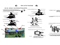
1
AP4040
WEB: www.yorkville.com
WORLD HEADQUARTERS
CANADA
U.S.A.
Yorkville Sound
Yorkville Sound Inc.
550 Granite Court
Pickering, Ontario
L1W-3Y8 CANADA
4625 Witmer Industrial Estate
Niagara Falls, New York
14305 USA
Voice: (905) 837-8481
Fax: (905) 837-8746
Voice: (716) 297-2920
Fax: (716) 297-3689
MODEL TYPE: YS4040
SERVICE MANUAL
Quality and Innovation Since 1963
Printed in Canada
Manual-Service-ap4040-00-4v0.pdf
IMPORTANT SAFETY INSTRUCTIONS
This lightning flash with arrowhead symbol, within
an equilateral triangle, is intended to alert the user to
the presence of uninsulated “dangerous voltage”
within the product’s enclosure that may be of sufficient
magnitude to constitute a risk of electric shock to persons.
The exclamation point within an equilatereal triangle is
intended to alert the user to the presence of important
operating and maintenance (servicing) instructions in
the literature accompanying the appliance.
Le point d’exclamation à l’intérieur d’un triangle équilatéral
est prévu pour alerter l’utilisateur de la présence
d’instructions importantes dans la littérature accompagnant l’appareil en ce qui concerne l’opération et la
maintenance de cet appareil.
Ce symbole d’éclair avec tête de flèche dans un triangle
équilatéral est prévu pour alerter l’utilisateur de la présence d’un
« voltage dangereux » non-isolé à proximité de l’enceinte du
produit qui pourrait être d’ampleur suffisante pour présenter
un risque de choque électrique.
S2125A
FOLLOW ALL INSTRUCTIONS
Instructions pertaining to a risk of fire,
electric shock, or injury to a person
SUIVEZ TOUTES LES INSTRUCTIONS
Instructions relatives au risque de feu,
choc électrique, ou blessures aux personnes
CAUTION: TO REDUCE THE RISK OF ELECTRIC
SHOCK, DO NOT REMOVE COVER (OR BACK).
AVIS: AFIN DE REDUIRE LES RISQUE DE CHOC
ELECTRIQUE, N’ENLEVEZ PAS LE COUVERT (OU LE
PANNEAU ARRIERE) NE CONTIENT AUCUNE PIECE
NO USER SERVICEABLE PARTS INSIDE.
REPARABLE PAR L’UTILISATEUR.
REFER SERVICING TO QUALIFIED
SERVICE PERSONNEL.
CONSULTEZ UN TECHNICIEN QUALIFIE
POUR L’ENTRETIENT
Read Instructions: The Owner’s Manual should be read and understood before operation
of your unit. Please, save these instructions for future reference and heed all warnings.
Clean only with dry cloth.
Packaging: Keep the box and packaging materials, in case the unit needs to be
returned for service.
Veuillez Lire le Manuel: Il contient des informations qui devraient êtres comprises avant
l’opération de votre appareil. Conservez. Gardez S.V.P. ces instructions pour consultations
ultérieures et observez tous les avertissements.
Nettoyez seulement avec le tissu sec.
Emballage: Conservez la boite au cas ou l’appareil devait être retourner pour réparation.
Warning: To reduce the risk or fire or electric shock, do not expose this apparatus to rain or
moisture. Do not use this apparatus near water!
Avertissement: Pour réduire le risque de feu ou la décharge électrique, n'exposez pas
cet appareil à la pluie ou à l'humidité. N’utilisez pas cet appareil près de l’eau!
Warning: When using electric products, basic precautions should always be followed,
including the following:
Attention: Lors de l’utilisation de produits électrique, assurez-vous d’adhérer à des
précautions de bases incluant celle qui suivent:
Power Sources
Your unit should be connected to a power source only of the voltage specified in the
owners manual or as marked on the unit. This unit has a polarized plug. Do not use
with an extension cord or receptacle unless the plug can be fully inserted. Precautions should be taken so that the grounding scheme on the unit is not defeated. An
apparatus with CLASS I construction shall be connected to a Mains socket outlet with
a protective earthing ground. Where the MAINS plug or an appliance coupler is used
as the disconnect device, the disconnect device shall remain readily operable.
Hazards
Do not place this product on an unstable cart, stand, tripod, bracket or table. The
product may fall, causing serious personal injury and serious damage to the product.
Use only with cart, stand, tripod, bracket, or table recommended by the manufacturer
or sold with the product. Follow the manufacturer’s instructions when installing the
product and use mounting accessories recommended by the manufacturer. Only use
attachments/accessories specified by the manufacturer
Note: Prolonged use of headphones at a high volume may cause
health damage on your ears.
The apparatus should not be exposed to dripping or splashing water; no objects
filled with liquids should be placed on the apparatus.
Terminals marked with the “lightning bolt” are hazardous live; the external wiring
connected to these terminals require installation by an instructed person or the use of
ready made leads or cords.
Ensure that proper ventilation is provided around the appliance. Do not install near
any heat sources such as radiators, heat registers, stoves, or other apparatus
(including amplifiers) that produce heat.
No naked flame sources, such as lighted candles, should be placed on the apparatus.
Power Cord
Do not defeat the safety purpose of the polarized or grounding-type plug. A polarized plug
has two blades with one wider than the other. A grounding type plug has two blades and a
third grounding prong. The wide blade or the third prong are provided for your safety. If the
provided plug does not fit into your outlet, consult an electrician for replacement of the
obsolete outlet. The AC supply cord should be routed so that it is unlikely that it will be
damaged. Protect the power cord from being walked on or pinched particularly at plugs. If
the AC supply cord is damaged DO NOT OPERATE THE UNIT. To completely disconnect
this apparatus from the AC Mains, disconnect the power supply cord plug from the AC
receptacle. The mains plug of the power supply cord shall remain readily operable.
Unplug this apparatus during lightning storms or when unused for long periods of time.
Service
The unit should be serviced only by qualified service personnel. Servicing is required
when the apparatus has been damaged in any way, such as power-supply cord or plug is
damaged, liquid has been spilled or objects have fallen into the apparatus, the apparatus
has been exposed to rain or moisture, does not operate normally, or has been dropped.
Alimentation
L’appareil ne doit être branché qu’à une source d’alimentation correspondant au
voltage spécifié dans le manuel ou tel qu’indiqué sur l’appareil. Cet appareil est équipé
d’une prise d’alimentation polarisée. Ne pas utiliser cet appareil avec un cordon de
raccordement à moins qu’il soit possible d’insérer complètement les trois lames. Des
précautions doivent êtres prises afin d’eviter que le système de mise à la terre de
l’appareil ne soit désengagé. Un appareil construit selon les normes de CLASS I
devrait être raccordé à une prise murale d’alimentation avec connexion intacte de mise
à la masse. Lorsqu’une prise de branchement ou un coupleur d'appareils est utilisée
comme dispositif de débranchement, ce dispositif de débranchement devra demeurer
pleinement fonctionnel avec raccordement à la masse.
Risque
Ne pas placer cet appareil sur un chariot, un support, un trépied ou une table instables.
L’appareil pourrait tomber et blesser quelqu’un ou subir des dommages importants.
Utiliser seulement un chariot, un support, un trépied ou une table recommandés par le
fabricant ou vendus avec le produit. Suivre les instructions du fabricant pour installer
l’appareil et utiliser les accessoires recommandés par le fabricant. Utilisez seulement
les attachements/accessoires indiqués par le fabricant
Note: L'utilisation prolongée des écouteurs à un volume élevé peut
avoir des conséquences néfastes sur la santé sur vos oreilles. .
Il convient de ne pas placer sur l’appareil de sources de flammes nues, telles que
des bougies allumées.
L’appeil ne doit pas être exposé à des égouttements d’eau ou des éclaboussures
et qu’aucun objet rempli de liquide tel que des vases ne doit être placé sur l’appareil.
Assurez que lappareil est fourni de la propre ventilation. Ne procédez pas à
l’installation près de source de chaleur tels que radiateurs, registre de chaleur, fours
ou autres appareils (incluant les amplificateurs) qui produisent de la chaleur.
Les dispositifs marqués d’une symbole “d’éclair” sont des parties dangereuses
au toucher et que les câblages extérieurs connectés à ces dispositifs de
connection extérieure doivent être effectivés par un opérateur formé ou en utilisant
des cordons déjà préparés.
Cordon d’Alimentation
Ne pas enlever le dispositif de sécurité sur la prise polarisée ou la prise avec tige de
mise à la masse du cordon d’alimentation. Une prise polarisée dispose de deux lames
dont une plus large que l’autre. Une prise avec tige de mise à la masse dispose de
deux lames en plus d’une troisième tige qui connecte à la masse. La lame plus large ou
la tige de mise à la masse est prévu pour votre sécurité. La prise murale est désuète si
elle n’est pas conçue pour accepter ce type de prise avec dispositif de sécurité. Dans
ce cas, contactez un électricien pour faire remplacer la prise murale. Évitez
d’endommager le cordon d’alimentation. Protégez le cordon d’alimentation. Assurezvous qu’on ne marche pas dessus et qu’on ne le pince pas en particulier aux prises.
N’UTILISEZ PAS L’APPAREIL si le cordon d’alimentation est endommagé. Pour
débrancher complètement cet appareil de l’alimentation CA principale, déconnectez le
cordon d’alimentation de la prise d’alimentation murale. Le cordon d’alimentation du
bloc d’alimentation de l’appareil doit demeurer pleinement fonctionnel.
Débranchez cet appareil durant les orages ou si inutilisé pendant de longues périodes.
Service
Consultez un technicien qualifié pour l’entretien de votre appareil. L'entretien est
nécessaire quand l'appareil a été endommagé de quelque façon que se soit. Par exemple
si le cordon d’alimentation ou la prise du cordon sont endommagés, si il y a eu du liquide
qui a été renversé à l’intérieur ou des objets sont tombés dans l'appareil, si l'appareil a été
exposé à la pluie ou à l'humidité, si il ne fonctionne pas normalement, ou a été échappé.
safety-4v7 • May 7/2008
AP4040 Parts List 3/17/2010
YS #
5906
5908
6419
6425
6438
6825
6934
6429
6432
6433
6439
6440
6450
6461
6463
6465
6822
6824
5101
5102
5103
5105
5106
5108
5113
5114
6854
6752
6814
6815
6873
6874
6925
6909
6910
7004
7005
6745
6840
5190
6478
6489
6517
6880
5401
5197
5203
5410
5412
5201
5208
5273
5416
5422
5209
5210
5834
6435
6451
5212
5226
5228
5229
5231
5234
5314
5882
5255
5258
5259
5269
5260
5282
5629
5945
5961
5267
5619
5621
5630
Description
RED 3MM LED 1V9 20MA.4SPCER T&R
GRN 3MM LED 1V9 20MA.4SPCER T&R
BRIDGE 35A 400V WIRE LEAD GI3504
BAV21 200V 0A25 DIODE
T&R
1N4007 1000V 1A0 DIODE
T&R
1N4148 75V 0A45 DIODE
T&R
MR854 400V 3A0 DIODE FASREC
1N4747A 20V0 1W0 ZENER 5% T&R
1N5248B 18V0 0W5 ZENER 5% T&R
1N5257B 33V0 0W5 ZENER 5% T&R
1N5225B 3V0 0W5 ZENER 5% T&R
1N750ARL 4V7 0W5 ZENER 5% T&R
1N5242B 12V0 0W5 ZENER 5% T&R
1N5240BRL 10V0 0W5 ZENER 5% T&R
1N5251BRL 22V0 0W5 ZENER 5% T&R
1N5250B 20V0 0W5 ZENER 5% T&R
1N4745A 16V0 1W0 ZENER 5% T&R
1N5246B 16V0 0W5 ZENER 5% T&R
BC550C
TO92 NPN TRAN T&R TB
BC560C
TO92 PNP TRAN T&R TB
MPSA06
TO92 NPN TRAN T&R TA
MPSA13
TO92 NPN DARL T&R TA
MPSA63
TO92 PNP DARL T&R TA
2N5401
TO92 PNP TRAN T&R TA
MPSA42
TO92 NPN TRAN T&R TA
MPSA92
TO92 PNP TRAN T&R TA
2N6517
TO92 NPN TRAN
TA
MTP10N15L TO220 NCH MFET
TN
MJF6668
T221D PNP TRAN DARL TJ
MJF6388
T221D NPN TRAN DARL TJ
MJE340
TO126 NPN TRAN
TG
MJE350
TO126 PNP TRAN
TG
MTP8P20
TO220 PCH MFET
TN
MJ21196
TO3 NPN TRAN
TH
MJ21195 TO3 PNP TRANSISTOR
TH
2SA2121-0 TO3P PNP TRAN
TK
2SC5949-0 TO3 NPN TRANSISTOR TK
LM13600N IC XCONDUCTANCE AMP
MC33078P IC DUAL OP AMP
MBS4992
TO92 8V5 DIAC T&R
AS35FN-TO92 TEMPERATURE SENSOR
__5R 20%
THERMISTOR-SURGR NTC
STM-BTB-600BRG TO220 ??A TRIAC 600V
4N35
OPTO-COUPLER
_10P 500V 5%CAP T&R RAD CER.2NPO
220P 100V 2%CAP T&R RAD CER.2NPO
_47P 100V 2%CAP T&R RAD CER.2NPO
100P 100V 10%CAP T&R BEAD
NPO
220P 100V 10%CAP T&R BEAD
NPO
470P 100V 5%CAP T&R RAD CER.2NPO
__2N2 400V 5%CAP T&R RAD .2FLM
__1N5 200V 5%CAP T&R RAD CER.2NPO
470P 50V 10%CAP T&R BEAD
NPO
__1N 50V 10%CAP T&R BEAD
NPO
__4N7 250V 5%CAP T&R RAD .2FLM
_22N 100V 10%CAP T&R RAD .2FLM
_10N 250V 20%CAP BLK RAD POLY FLM
_22N 275V 20%CAP BLK 'X2' 15MM AC
__4N7 250V 20%CAP BLK 'Y' 10MM AC
100N 63V 5%CAP T&R RAD .2FLM
_68N 100V 5%CAP T&R RAD .2FLM
100N 100V 5%CAP T&R RAD .2FLM
150N 63V 10%CAP T&R RAD .2FLM
220N 63V 10%CAP T&R RAD .2FLM
470N 63V 10%CAP T&R RAD .2FLM
100N 50V 10%CAP T&R BEAD
X7R
220N 250VDC 10%CAP BLK RAD PLY FLM
__1U 63V 20%CAP T&R RAD .2EL
__4U7 63V 20%CAP T&R 8X7MM .2EL
__4U7 63V 20%CAP T&R RAD .2
__4U7 100V 20%CAP T&R RAD LESR2
_22U 50V 20%CAP T&R RAD .2EL
_10U 16V 20%CAP T&R 5X7MM .2NP
_10U 160V 20%CAP BLK 10X13MM EL
_10U 63V 20%CAP T&R RAD .2EL
_33U 16V 20%CAP T&R RAD .2
100U 25V 20%CAP T&R RAD .2EL
330U 100V 20%CAP BLK 12X25MM EL
470U 63V 20%CAP BLK 12X25MM EL
330U 25V 20%CAP BLK 10X13MM EL
Qty.
3
3
2
4
15
52
20
1
2
4
2
9
4
1
1
1
4
2
14
14
3
2
1
2
2
2
3
2
1
2
6
6
2
16
16
2
2
2
5
2
2
2
2
4
4
3
2
2
13
2
12
2
2
2
2
11
2
2
1
4
4
3
4
2
4
2
4
3
2
4
2
8
2
4
2
12
3
4
1
6
YS #
5896
4390
4520
2448
3820
3485
3486
3489
3490
3601
3410
3415
3918
3628
3417
3657
3451
9198
7584
8432
8434
3894
3501
3803
3810
3827
3852
2328
2329
4056
8433
8661
8437
3468
3821
8261
8701
8793
8760
8800
8854
8720
8797
3797
3846
3916
4060
8432P
4597
4599
5299
4745
4749
2005
2006
4677
4688
4911
4748
4733
2009
2037
4605
4875
4930
2039
2014
2016
2041
4899
2042
4811
4984
2045
2021
2023
4857
4977
2024
4867
Description
4700U 80V 20%CAP BLK 25X50MM ELS
_10K
AUD 16MM DETENT
P22
_10K
TRIM POT
15.00 AMP CIRCUIT BREAKER
___4UH COIL 14AWG ZOBEL HORIZONTAL
CLIP 250X032 18-22AWG RIGHT ANGL
CLIP 250X032 22-18AWG DISCO-LOK
CLIP 250X032 18-22AWG DISCO/INSL
CLIP 250X032 14-16AWG DISCO/INSL
RING TERMINAL 16AWG WIRE & #8 SCREW
RED:LEFT/BLACK:RIGHT BIND POST TPP5
RED:RIGHT/BLACK:LEFT BIND POST TPP5
1/4" JCK PCB MT HORZ SLIM W/SCREW
SPKON 4C PCB MT VERT 250TAB GRY #4
6-32 SCREW TERMINAL PC MNT SNAP-IN
XLR FEML PCB MT HORZ NO SHELL
EYELET SMALL 0.089 OD PLATED
FAN 80MM X 80MM 40CFM 12VDC
SQUARE-CUT O RING FOR AP AIR FILTER
AP SERIES AIR GRILL BLACK PLASTIC
AP SERIES PLASTIC HANDLE PAIR
AAVID 5972-B H/S W/TAB B.O.
B52200F006 COMP WASH #4 SMALL
NYLON SECUR-A-TACH MINI PLASTIC TIE
4" NYLON CABLE TIE
SQUARE BUMPER BUTTON BLACK
STICK ON CABLE WRAP ANCHOR
8 CIR XH-HEADER 0.098IN
12 CIR XH-HEADER 0.098IN
2 CIR XH-HEADER 0.098IN
KNOB AP SERIES PLASTIC
KNOB BUTTON
FLAT GREY
FAN FILTER LABEL
8' 3/16 SJT AC LINE CORD STRIP 17"
STRAIN RELIEF HEYCO #1200
GE VELVET/MATTE LEXAN .007"X12"X24"
4-40 KEPS NUT ZINC
4-40 HEX NUT ZINC
6-32 KEPS NUT TIN PLATED
6-32 KEPS NUT ZINC
6-32 X 1/4" 0.D. HEX NUT ZINC CLEAR
#8 SPRING NUT
5/16-18 KEPS NUT JS500
TO-247 THERMO CONDUCTIVE PAD
TO220 THERMO PAD LARGE HOLE 56359B
TO3 SIL-PAD REPLACES MICA
SILPAD 1500ST 0.900 X 0.725BERQUIST
LOGO HOT STAMPED ON PLASTIC GRILL
22AWG STRAN TC WIR
JMP
22AWG SOLID SC WIR
T&R JMP
24AWG SOLID SC WIR
RAD JMP
5.0W 0R1 5%
BLK RES
5.0W 0R15 5%
BLK RES
1.0W 0R47 5%FLAME PROOF T&R RES
1.0W 1R 5%FLAME PROOF T&R RES
1/2W 1R 5%
T&R RES
1/2W 2R2 5%
T&R RES
1/4W 2R2 5%
T&R RES
2.0W 3R9 5%
T&R
5.0W 5R6 5%
BLK RES
1/4W 10R 2%FLAME PROOF T&R RES
1/4W 10R FUSIBLE
T&R RES
1/8W 10R 5%
T&R RES
1/4W 10R 5%
T&R RES
1/4W 10R 5% .2"U
T&R RES
1/4W 22R0 FUSIBLE
T&R RES
1/8W 33R 2%FLAME PROOF T&R RES
1/8W 39R 2%FLAME PROOF T&R RES
1/4W 39R0 FUSIBLE
T&R RES
1/4W 39R 5%
T&R RES
1/4W 47R0 FUSIBLE
T&R RES
1/4W 68R 5%
T&R RES
1/4W 150R 5%MINI
T&R RES
1/4W 150R FUSIBLE
T&R RES
1/4W 200R0 1%FLAME PROOF T&R RES
1/8W 220R0 1%FLAME PROOF T&R RES
1/4W 220R 5%
T&R RES
1/4W 220R 5%MINI
T&R RES
1/8W 249R 2%FLAME PROOF T&R RES
1/4W 270R 5%
T&R RES
Qty.
16
2
2
1
2
4
14
3
4
2
1
1
2
2
1
2
68
1
1
1
1
8
23
1
12
11
1
4
2
1
2
3
1
1
1
0.348
20
3
64
5
4
2
1
4
8
32
4
1
23
120
10
12
4
2
4
4
3
8
4
2
2
6
1
2
1
2
4
2
10
6
4
2
4
8
6
4
2
7
12
2
YS #
4986
4855
4821
4980
4891
5019
4873
4934
4981
4854
4988
4791
4808
6113
4847
6124
4826
6136
4744
4681
4943
4982
4887
4990
4762
4800
4829
4983
6116
4856
5008
4630
4830
4771
6125
6123
4777
4632
6118
4833
4840
6122
4878
6119
4835
6139
5007
4586
4898
4838
6120
4851
4886
4668
6126
6127
4844
4948
4951
6132
4751
3618
3604
3699
3735
8870
8865
8729
8742
8861
8741
8871
8902
8799
8832
8801
8829
8761
8796
8830
Description
1/4W 270R 5%MINI
T&R RES
1/4W 330R 5%
T&R RES
1/4W 470R 5%
T&R RES
1/4W 470R 5%MINI
T&R RES
1/4W 620R 5%
T&R RES
1/4W 620R 5%MINI
T&R RES
1/4W 680R 5%
T&R RES
1/4W 1K 5% .2"U
T&R RES
1/4W 1K 5%MINI
T&R RES
1/4W 1K2 5%
T&R RES
1/4W 1K5 5%MINI
T&R RES
1/4W 1K54 1%
T&T RES
1/4W 2K 5%
T&R RES
1/4W 2K 5%MINI
T&R RES
1/4W 2K2 5%
T&R RES
1/4W 3K 5%MINI
T&R RES
1/4W 3K3 5%
T&R RES
1/4W 3K3 5%MINI
T&R RES
5.0W 3K6 5%
BLK RES
1.0W 4K7 5%
T&R RES
1/4W 4K7 5% .2"U
T&R RES
1/4W 4K7 5%MINI
T&R RES
1/4W 7K5 5%
T&R RES
1/4W 8K2 5%MINI
T&R RES
1/4W 9K760 0.1% *** T&R RES
1/4W 10K0 1%
T&R RES
1/4W 10K 5%
T&R RES
1/4W 10K 5%MINI
T&R RES
1/4W 10K0 1%MINI MF
T&R RES
1/4W 12K 5%
T&R RES
1/4W 14K7 1%
T&R RES
1/2W 15K 5%
T&R RES
1/4W 15K 5%
T&R RES
1/4W 17K8 1%
T&R RES
1/4W 18K 5%MINI
T&R RES
1/4W 20K0 1%MINI MF
T&R RES
1/4W 21K5 1%
T&R RES
1/2W 22K 5%
T&R RES
1/4W 22K 5%MINI
T&R RES
1/4W 27K 5%
T&R RES
1/4W 33K 5%
T&R RES
1/4W 33K 5%MINI
T&R RES
1/4W 43K 5%
T&R RES
1/4W 47K 5%MINI
T&R RES
1/4W 56K 5%
T&R RES
1/4W 62K 5%MINI
T&R RES
1/4W 78K7 1%
T&R RES
1/4W 82K 5%MINI
T&R RES
1/4W 91K 5%
T&R RES
1/4W 100K 5%
T&R RES
1/4W 100K 5%MINI
T&R RES
1/4W 120K 5%
T&R RES
1/4W 200K 5%
T&R RES
2.0W 220K 5%10MM BODY T&R RES
1/4W 220K 5%MINI
T&R RES
1/4W 470K 5%MINI
T&R RES
1/4W 1M 5%
T&R RES
1/4W 1M 5% .2"U
T&R RES
1/4W 4M7 5% .2"U
T&R RES
1/4W 8M2 5%MINI
T&R RES
1/4W 22M 5%
T&R RES
STAR RING TERMINAL14-16AWG #10SCREW
21" 14C-28AWG DIP HDR CABLE .05"
RELAY 1C 02AMP DC48 006MA PC-S
RELAY 1A 16AMP DC48 011MA PC-C
#4 X 1/4 PAN PH TYPE A ZINC
4-40 X 5/16 PAN PH MS JS500
#4 X 3/8 FLAT QUAD TYPE A JS500 BLK
4-40 X 3/8 PAN PH TAPTITE JS500
4-40 X 3/8 PAN PH MS JS500
4-40 X 1/2 PAN PH MS JS500
4-40 X 5/8 PAN PH MS JS500
4-40 X 3/4 PAN PHIL MS B/O & WAX
#6 X 1/4 PAN PH TYPE B JS500
6-32 X 1/4 PAN PH TAPTITE JS500
6-32 X 3/8 PAN PH TAPTITE JS500
6-32 X 3/8 FLAT PH TAPTITE BO#C HEA
6-32 X 1/2 PAN PHIL MS ZINC CLEAR
6-32 X 5/8 PAN PH TAPTITE ZINC
6-32 X 7/8 PAN PH MS JS500
Qty.
2
2
2
9
2
2
1
1
15
1
6
4
4
2
2
6
2
2
8
2
1
17
5
2
8
2
2
9
12
4
2
2
12
2
2
4
2
8
1
6
3
1
2
9
8
2
2
2
4
2
2
2
1
2
10
2
1
1
2
2
4
4
1
1
1
2
2
4
2
8
3
12
4
2
4
4
24
64
2
2
YS #
8869
8999
8719
8815
8809
8749
8731
8740
3570
8663
8629
3751
3743
3851
3859
8657
8921
8667
3517
8818
3511
8485
8850
3502
3436
3587
3705
3682
3035
3036
3037
CH1197
8379
Description
8-18 X 1/2 THRD CUTTING FOR PLASTIC
8-32 X 5/8 PAN PH TAPTITE JS500
8-32 X 3/4 FILLISTER PHIL MS JS500
8-32 X 3/4 PAN PH TAPTITE JS500
10-32 X 1/4 PAN PH TAPTITE JS500
10-32 X 1/2 QDX PH TAPTITE JS500
10-16 X 5/8 TYPE B HEX W/SLOT JS500
5/16-18 X 3 GRD 5 HEX BOLT JS500
14 PIN SCKT CLOSED FRAME DIP ONLY
11/64 NYLON SPACER (MICRO PLASTIC)
10-32 X 1/4 SPACER PHENOLIC
SNAP IN 5/16 SPACER RICHCO
SNAP ON 0.5" SPACER RICHCO
1/2 PCB PLASTIC SPACER
1/2 PLASTIC HEX SPACER #4
6-32 X 3/8" HEX SPACER ALUMINUM
#3MM ID3.2MM OD7.0MM THICK 5MM
SHOULDER WASHER SWS-229 LENGTH 1/8
NYLON WASHER #8 0.062
3/4 OD X 3/8 ID X .080 THICK WASHER
#6 FLAT WASHER NYLON
#6 SPLIT WASHER ZINC
#10 INT TOOTH LOCKWASHER BO
NYLON FLAT WASHER OD.158ID.110H.070
DPDT PUSH SW PCMT H BREAK B4 MAKE
DPDT ROKR SW QUIK 250"AC/PWR ON-OFF
4P3T SLID SW PCMT H
250 MALE PCB TAB REEL
PATCH 08 22AWG 05.0 XH
PATCH 08 22AWG 09.0 XH
PATCH 12 22AWG 15.0 XH
AP4040 117VAC-IMPORT
T'RD
1/4 X 6 X 2.3 10PP1 FILTER FOAM
Qty.
4
17
2
5
5
13
12
1
1
66
16
3
5
4
2
2
4
4
4
2
2
4
4
2
3
1
1
36
1
1
1
1
1
Yorkville Sound • http://www.yorkville.com
SERVICE MANUAL
Yorkville AP4040 Power Amplifier
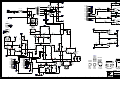
M1129 “THE INPUT BOARD”
The input board processes the audio signal from the input jacks to the volume control
board, (M1128).
Each channel consists of a balanced gain stage, switchable subsonic filter, and a
stereo / mono / bridge switch.
Looking at the left channel, the balanced input, (XLR Jack) and unbalanced input
(phone jack) are wired in parallel to the input of a balanced operational amplifier, (U4).
The gain of this stage is 0.82 (-1.3dB) balanced and 1.6 (4.0dB) unbalanced. Resistors
R25, R27 along with capacitors C11 and C12 form a radio interference elimination filter.
Switch S1 selects the cutoff frequency of the hi-pass subsonic filter. The subsonic
filter provides a 20Hz or 40 Hz high pass filter. The filter consists of a tee network on
the input of U3 along with R10, R28, C29 and C30, C33 and C34. The gain is 1 (0dB)
in the passband, (above 100Hz).
The audio signals from the input board M1129 pass through the 14 conductor cable
to board M1128.
M1128 “VOLUME CONTROL BOARD”
This board contains:
• the front panel audio gain controls
• the front panel indicating LED’s (power, protect, activity and clip).
• the audio limiters
Circuit Explanation:
• The left channel of the circuit is explained.
(Refer to the schematic of M1128 as the sections of the circuit are explained.)
The audio signal out of M1129 passes through volume control P2 and the desired
level enters U2 through pin 6. U2 is set for a gain of 5 (14dB) when the volume control
is in the fully clockwise position.
The AP4040’s defeatable limiter is built around LD8. LD8 is an opto-resistive cell
comprising of an LED that shines on a photocell. As the LED in the LD8 becomes
brighter, the resistance of the photocell decreases, placing more of the audio signal on
pin 5 (non-inverting input) of U2. This audio voltage gets subtracted from the signal on
the inverting input and less signal appears on the output of U2. Transistors Q5 and Q6
along with the surrounding passive parts provide the attack and release time constants
of the limiting function along with the drive currents for the clip LED and the LED
inside LD8. When an audio signal on the output of the power amplifier section (on
board M1146) enters clipping, pulses representing the duration of the clipped portion
appear at LCLIP. These pulses turn on transistor Q6, and Q6 provides current pulses
to turn on clip LED LD6. The pulses also pass through R7 and D6 to charge C3 and
C36. When the voltage across C3 reaches 0.5 volts then Q5 turns on providing a current into the LED of the LD8 limiting the audio signal at U2. The charging (attack) and
discharging (release) times of the limiter are 80mS and 3.5 seconds respectively.
Resistors R50 and R7 provide the charging path, and resistor R51 provides the discharge path. The limiter can be defeated by placing the limiter switch (S2) in the in
position which disconnects Q5 and the charging / discharging circuitry from V+.
1
Yorkville Sound • http://www.yorkville.com
SERVICE MANUAL
The activity LED circuit consists of Q1 and the surrounding circuitry. The audio signal enters the activity LED circuit through R2. R2 and C21 form a differentiator that
turns Q1 on illuminating the activity LED whenever the audio signal increases in amplitude. A constant current flows through R55A, R55B and when Q1 is off, the collector
current then flows through D1.
From M1128 the audio signal passes through a 12-conductor ribbon cable to circuit
board M1147.
On M1127 an operational amplifier U201 re-references the ground for the audio signal from LREF or RREF to the corresponding LOG (left output ground) or ROG (right
output ground). U201 also provides DC correction for DC offsets appearing on the output binding posts. Feedback from the output binding posts appears on LFNB or RFNB.
Through R203A or R203B the DC offset achieves a gain of -1 from U201. The DC offset of opposite polarity on the output of U201 will compensate for the DC offset in the
amplifier section on M1146 resulting in 0 volts DC on the output binding posts.
• The audio signal continues to M1146 via an 8-conductor ribbon cable.
M1126 “THE VOLTAGE AMPLIFIER AND
CURRENT AMPLIFIER”
This board contains:
• a voltage amplifier section
• a current amplifier section
• amplifier current limit section
• DC output protection
• heatsink temperature sensing
Voltage Amplifier Section
The voltage amplifier amplifies the audio signal’s voltage from 6.8 volts peak (at the
output of U201) to approximately 98v peak, which is required to drive the current
amplifier section. The current amplifier provides the current required for the 98v peak
signal to drive 1200 watts into 4 ohms out of the binding posts.
Before the circuit is described in detail here is a quick rundown on the signal’s path
through the voltage amplifier stage. Refer to the schematic of M1146. Let’s consider
that a positive going AC signal is present at the SIG input. The positive going signal
will turn on the positive side of the voltage amplifier. The signal at the SIG input turns
on Q12A (through R40A, D14A and D13A). The collector of Q12A pulls down on the
base of Q14A turns this transistor on further and allows a greater current to flow out of
Q14A’s collector. This increase in current passes through Q15A and it’s collector to
emitter voltage decreases. The collector of Q15A now being more positive in voltage
turns the base of Q18A on causing an increase in Q18A’s collector current resulting in
test point 1 going positive.
As the positive side of the amplifier was turning on the negative side would have
been turning off. This is how test point 1 was able to move positive following the input
signal. The reverse would hold true if a negative going signal were present on the input
of the voltage amplifier.
550 Granite Court, Pickering, Ontartio CANADA L1W-3Y8
550 Granite Court, Pickering, Ontartio CANADA L1W-3Y8
4625 Witmer Industrial Estate, Niagara Falls, New York USA 14305
4625 Witmer Industrial Estate, Niagara Falls, New York USA 14305
1
Yorkville Sound • http://www.yorkville.com
SERVICE MANUAL
Yorkville Sound • http://www.yorkville.com
SERVICE MANUAL
CIRCUIT DESCRIPTION:
The voltage amplifier is a mirrored image with circuitry connected to the positive power
supply rail being identical (but opposite polarity) to the circuitry connected to the negative power supply rail.
For this reason we will look in detail at the positive side of the amplifier.
The audio signal enters the voltage amplifier at the SIG input. The signal passes
through R40A, D14A and D13A to the base of Q12A. Diodes D13A and D14A set up
the DC bias on Q12A to approximately 0.6 mA.
The first voltage gain stage consists of Q12A along with the resistor chain on its collector and the emitter resistor (R44A).
Transistor Q12A drives the base of Q14A through the resistor chain. A DC current of
approximately 4 mA should flow through the collector of Q14A. The voltage drop
across Q14A remains constant and is derived from the voltage drop across the voltage
reference Q20A, resistor R58A, and the base/emitter junction of Q15A. This total voltage should equal approximately 3 VDC. Transistor Q14A is the second gain stage and
its output current flows through Q15A. Transistor Q15A is a common base stage with
the collector driving the base of output buffer Q18A.
Diode D17A is a clamping diode that prevents the maximum peak of the audio signal from coming within 4V of the 144 VDC rail. This is to prevent the output current
amplifier from going into saturation during clipping and therefore having storage delay
problems.
Transistor Q18A buffers the high impedance present on the collector of Q15A. The
output of the buffer provides a low output impedance at the junction of R61A and
R62A and is current limited to 30mA through the clamping action of D19A, D20A and
D23A. The signal at the junction of R61A and R62A drives the succeeding current
amplifier.
Current Amplifier Section
The current amplifier receives a high voltage audio signal from the voltage amplifier
and provides the current drive necessary to drive speaker cabinets.
The current amplifier is a two-tier complimentary output driver design controlled by a
complimentary darlington stage.
[CIRCUIT DESCRIPTION - REFER TO THE SIMPLIFIED SCHEMATIC #1 ON THE
FOLLOWING PAGE]
QUIESCENT CONDITION:
This design is class A/B and therefore the output driver transistors must be forward
biased to provide low crossover distortion. In most class A/B designs, a diode chain or
VBE multiplier is used to control the bias voltage and provide a means of adjusting the
bias. This design is different, as there isn’t a diode chain or VBE multiplier. For simplicity lets consider only the positive side of the current amplifier, that is all parts between
the positive power supply rails and the audio signal output/input terminals. The negative side is the same as the positive, except for polarity changes.
To bias Q14, greater than 0.5V is needed from base to emitter, (or for simplicity from
base to amplifier output). Points A and B are at the same potential, so consider them
to be connected. If this is true then 0.5V from test point 2 to the amplifier output must
appear across R12. There must be some way of developing this voltage across R12,
and there is using the darington (Q5 and Q40) driver along with local feedback.
Simplified schematic #1 shows the biasing circuit. The current needed to develop 0.5V
across R12 comes from the emitter of Q5. When the amplifier is first turned on the current
source (Q3) turns on Q5 and Q40) and current flows through R12 developing a voltage.
When this voltage approaches 0.5V Q1 turns on and robs current from the base of Q40.
2
550 Granite Court, Pickering, Ontartio CANADA L1W-3Y8
550 Granite Court, Pickering, Ontartio CANADA L1W-3Y8
4625 Witmer Industrial Estate, Niagara Falls, New York USA 14305
4625 Witmer Industrial Estate, Niagara Falls, New York USA 14305
2
Yorkville Sound • http://www.yorkville.com
SERVICE MANUAL
This causes Q40 to turn off until the reduced current flowing through Q5 maintains
0.5V across R12. Q1 will turn off slightly causing Q5 and Q40 to increase their collector
currents. The circuit reaches a point of equilibrium with approximately 0.5V across R12.
Because all output devices are not identical and base emitter voltages vary, some
adjustment must be available to slightly adjust the 0.5V across R12. This is accomplished with RT1. RT1 causes Q1 to turn on slightly more or less resulting in Q5 and
Q40 turning on slightly more or less and therefore R12’ s voltage will be slightly more
or less than 0.5v. The proper quiescent current voltage is 4mV (to be measured
between test points 8 and 9).
The Second Tier and Tier Switching
Refer to the simplified schematic Fig. #1 while reading the following text. One way of
making an amplifier more efficient is to vary the Power Supply Voltage on the collectors of the output transistors (Q14 & Q22). The lower the voltage from collector to emitter, the lower the device dissipation. During quiescent conditions, there is 55VDC on
the collectors of output transistors Q14 and Q22. The peak AC voltage that can appear
on the amplifier’s output is approximately 139V peak. How can an output transistor
deliver a 139V peak when its collector is only at 78VDC? It can if its collector is pulled
up to 144VDC as the output signal’s peak rises above 78VDC. Refer to Fig. #2. The
second tier voltage must remain above the amplifier’s output voltage by amount Vm.
Therefore the circuitry controlling the second tier voltage must increase the tier voltage
before the amplifier’s output voltage reaches 78VDC. This leading voltage is necessary
to compensate for time lag of the second tier circuit during fast rising amplifier output
signals.
The voltage between the amplifier’s output
and test point 4 is approximately 12VDC
derived from the voltage drop across ZD4. We
call this voltage the “floating battery” because it
floats on top of the output audio signal with test
point 4 always being 12VDC greater than the
peak of the output signal. Test point 4 drives the
gate of mos-fet Q11. Q11 controls the transistors of the upper tier. As Q11 turns on its source
forward biases the base of Q13 and Q13 pulls
the collector of Q14 towards the 100 volt rail.
The gate to source voltage needed to turn on
Q11 is approximately 3.5 volts. When the peak
output signal is about 69.5vp (78v-(12v-3.5v))
then Q11 will start to turn on the second tier.
The second tier voltage will remain about 13
volts (Vm) above the peak of the output signal
to the point of clipping where this voltage is reduced to about 6 volts (measured driving an 8 ohm load). Zener ZD8 protects the gate source junction of Q11 and also provides a supply current path through R29 for the “floating battery”.
Yorkville Sound • http://www.yorkville.com
SERVICE MANUAL
amount of time was spent on the current limit circuitry so that it may simulate the safe
operating area of the output transistors (SOAR curve). No matter how reactive the load
may be the phase shift that it presents, along with it’s resistive component is used to
set the output current limit of the output transistor stage.
Refer to the schematic of board M1146 while reading the following text. The current
limit circuitry is a mirrored image with circuitry connected to the positive power supply
rail being identical (but opposite polarity) to the circuitry connected to the negative
power supply rail. For this reason we will look at the positive side of the circuitry.
Transistor Q9 measures the peak current flowing through resistor R53. The voltage
across R53 (as a result of the current flowing through it) is scaled down by R55, R35,
R35A, R36, R37, D7 and D11 these parts make up the safe operating area along with
the time constants of C30, R34, C12 and R26. Fig. #3 shows a waveform of the current
that passes through R52 and R53 when the output of the amplifier is shorted to ground.
This can only be seen by using an oscilloscope to measure differentially across R52
and R53. The conditions of the measurement are contained on the diagram. During current limit when Q9 turns on it reduces the voltage across R42. R42 is in series with a
16 volt zener (ZD7) and is also in parallel with the junction of Q8. The current that flows
through R20, ZD7, R42, and R22 normally saturates Q8. When Q9 reduces the voltage
across ZD9 and R42 to below 16.6 volts, Q8 turns off allowing a charge to build up on
C8 through resistors R24 and R25. If current limiting occurs for a long enough duration
to allow C8 to charge to 1.2 volts then Q7 will turn on tripping the relay circuit on board
M1147. As soon as the relay is tripped the audio signal will be turned off at the output
of the voltage amplifiers and will remain off for about 5 seconds before the relay turns
on and allows the audio signal to pass through the amplifier. If a current limit condition
is still present then the whole cycle will occur again and repeat until the load conditions
on the amplifier’s output are safe for the amplifier. When a safe load appears the amplifier will automatically reset and drive that load (the speaker cabinet).
DC Protection
If a DC voltage greater than 8 volts appears on the output of the amplifier for more
than 200 milliseconds then triac Q30 will turn on holding the output at ground potential. MBS4992 is a device that turns on at either + or - 8 volts DC.
NOTE: The Power supply voltages given are those when the amplifier is not driving a
speaker load. This will allow yo to check the tier switching with the cover of the amplifier off and the amplifier, therefore, running cool.
Current Limit Protection Circuitry
To have an amplifier drive 3000 watts into practically any combination of speaker cabinets and know what is a safe load and what is not is a very difficult task. An extensive
3
550 Granite Court, Pickering, Ontartio CANADA L1W-3Y8
550 Granite Court, Pickering, Ontartio CANADA L1W-3Y8
4625 Witmer Industrial Estate, Niagara Falls, New York USA 14305
4625 Witmer Industrial Estate, Niagara Falls, New York USA 14305
3
Yorkville Sound • http://www.yorkville.com
SERVICE MANUAL
NOTE: Every time you replace blown output transistors on a
M1146 board test the DC protection triac with the following circuit.
Conditions of test:
A) Pass a 100Hz 25v peak signal through the M1126 board under test with no load
connected to the amplifier output.
B) Connect points 1 and 2 as shown in the diagram. The amplifier should go into protect mode as the triac (if working) shorted the output of the amplifier to ground, and
the amplifier goes into current limit.
C) Disconnect the triac test circuit and allow the amplifier to complete it’s protect cycle.
D) Reverse connections 1 to 2 and 2 to 1 and test again. The same results as in B)
should be observed if the triac is working.
Only test the triac for one protect cycle as
prolonged testing will heat the triac to a high temperature.
Yorkville Sound • http://www.yorkville.com
SERVICE MANUAL
If prolonged current limiting occurs on the amplifier’s output transistors then D204 or
D205 (depending on which channel is current limiting) will be forward biased turning on
Q202 (from its off state). Now +144VDC appears on the collector of Q202 and through
R210 and R211 turn on Q203 therefore turning off Q201 by shorting its base emitter
junction. Q201 turning off will turn the relay off and the normally closed contacts (off
state) will short the outputs of the voltage amplifiers to ground so as not to continuously
stress the amplifier’s output transistors. A cycle now occurs. With the voltage amplifiers
now disabled there is no signal driving the output transistors (Q13 to Q28).
The current limit circuit protecting the output transistors (Q13 to Q28) turns off and
D204 and/or D205 are not forward biased and Q202 turns off. Through Q203 and
Q201 the relay is turned back on and the voltage amplifiers are now active again, driving the output transistors. If current limiting still occurs, then the same cycle will occur.
If the cause of current limiting (low impedance or short on the speaker output terminals) has been removed, then the amplifier will continue to operate normally.
The third operation that the relay provides is “overheat shutdown”. If for some reason the fan cannot keep the heatsinks in a safe operating temperature area then the
fan control circuit (on board M1147) will deliver through D207 a positive current to turn
Q203 on and turn Q201 off to turn off the relay and disable the voltage amplifiers.
When the fan has cooled down the temperature of the amplifier, then the signal
through D207 will disappear and the relay circuit will turn on the relay to resume normal operation. Anytime the relay is in the “protect” mode (due to the abnormal states)
then contact pin 4 of the relay will illuminate LD3 (the protect LED on the front panel).
Soft Turn On Circuit
To reduce the “inrush” current that flows through the line cord from the 120 VAC power
source (typical with large linear power supplies), a circuit provides a soft turn on function. When the power switch is turned on, the current that initially flows through the primary of the transformer must flow through SG201 and SG202. These are surgestors
that reduce the peak inrush current flow. After about 500 milliseconds a relay’s contacts short across the surgestors so that they are not stressed by the current flowing
through them under normal operation. A circuit consisting of Q240, Q241, C215, and
the associated resistors provides the time delay for the turn on cycle of the relay. The
circuit is very similar to the shutdown time delay circuit. Refer to the section on the
shutdown circuit for a circuit description.
M1147 SHUTDOWN CIRCUIT, FAN CONTROL CIRCUIT,
and SOFT TURN ON CIRCUIT:
4
• The shutdown relay and its associated drive circuitry have two possible
operating states.
• Amplifier on under normal operating conditions.
• Amplifier power switch has just been turned OFF/ON, or the amplifier is in current
limit protecting the amplifier’s output transistors, or the amplifier has overheated.
Shutdown Circuit
Here is how the circuit accomplishes these functions. The relay’s normally closed contacts short the output of the voltage amplifiers to ground when the power switch is off.
When the power switch is turned on, the relay remains off (normally closed) for about
6 seconds. C203 charges to 35V and results in Q203 turning off allowing Q201 to turn
on. As Q201 turns on, it connects the negative terminal of the relay’s coil (Pin 16) to
ground energizing the relay and opening the normally closed contacts.
Fan Circuit
Looking at the schematic to board M1147, here is a
quick explanation of the fan control circuit. There is
a temperature sensor (AS35) on each M1146
board. When the amplifier is first turned on, Q207
and Q208 are off. The AS35 temperature sensors
are configured as temperature controlled current
sources. As either temperature sensor begins to
heat up, more current flows through D212 or D218
increasing the voltage drop across R235 or R236.
The hotter temperature sensor will provide more
current than the cooler sensor and therefore develop a higher voltage across it’s associated 8K2
resistor. The higher voltage will forward bias D212
or D218 reverse biasing the cooler temperature
sensor’s diode so that the hotter sensor will control the fan speed. At 40 degrees C there
550 Granite Court, Pickering, Ontartio CANADA L1W-3Y8
550 Granite Court, Pickering, Ontartio CANADA L1W-3Y8
4625 Witmer Industrial Estate, Niagara Falls, New York USA 14305
4625 Witmer Industrial Estate, Niagara Falls, New York USA 14305
4
Yorkville Sound • http://www.yorkville.com
SERVICE MANUAL
Yorkville Sound • http://www.yorkville.com
SERVICE MANUAL
is 10 volts across R235 or R236 which is enough to turn on Q210, Q208, and Q207 providing 7 DC volts to the fan. Further heating the temperature sensors results in a larger
DC voltage across the fan. To lower the dissipation of Q207, D215, D216, ZD205, ZD206
and R226 turn off Q207 and Q208 when the full wave rectified voltage present of the collector of Q207 reaches approximately 58V by robbing current from the base of Q208.
The maximum fan voltage is 20.5 VDC. ZD207 and R228, R229 and R230 provide a current limiting function. Figure #4 shows the current through these resistors when there is
12VDC across the fan.
Thermal Shutdown Circuit
The emitter of Q210 in the fan circuit is the measuring point for the shutdown voltage.
As the temperature sensing devices (AS35) that control the fan circuit heat up the voltage on the emitter of Q210 rises until at 85 degrees Celsius on the M1146 heatsinks.
The voltage on the emitter of Q210 reaches 18 (85 degrees C) VDC and the amplifier
must be shutdown to protect the output power transistors. ZD202 and D207 become
forward biased and Q203 turns on turning the relay off and muting the audio signal.
After the amplifier cools down the voltage will decrease until Q37 turns off turning the
relay back on enabling the amplifier.
Identifying Defective Boards in the AP4040
STEP 1: VISUAL INSPECTION OF FRONT PANEL AND FAN
• Check to see whether the green power LED is lit. If not, the amplifier has a
power supply (M1147 board), transformer, A.C. switch or line cord problem.
• If the red protect LED stays on or samples off and on, this usually indicates a
problem with the voltage amplifier or current amplifier sections on one or both of
the M1126 boards. Check for misaligned pin connections or see if the ribbon
cables have been cut or pinched through their insulation.
• If the fan is running at full speed at power up this usually indicates a problem
with the fan circuitry on the M1147 board, but it can also be caused by M1146 circuit problems. A damaged AS35 temperature sensor located under the M1146
heatsinks can cause erratic fan behavior.
• No output on either or both channels could be caused by intermittent push
switches on the input board.
STEP 2: VISUAL INSPECTION OF INTERNAL CHASSIS AND INITIAL TESTING
After removing the lid, look for any signs of smoke, charring or burnt components.
Before powering up replace the burnt components, and check the associated circuitry
for damaged parts. Disconnect one M1127 board and test one board at a time to
reduce the possibility of further damage. Use a variac to slowly increase the 120 VAC
up from 0 volts while monitoring the quiescent current with a meter and the speaker
output with an oscilloscope. Watch the speaker output for large DC offsets, or oscillation. Watch the meter for large collector currents flowing. Remember under quiescent
conditions, there should only be 3 to 5 millivolts across test points 8 and 9 on the output stage of the amplifier.
5
SPECIFICATIONS
Frequency Response:
Hum and Noise:
THD (1 khz, 4–Ohms):
THD(20Hz – 20kHz, 4–Ohms):
High Pass Filter:
Slew Rate:
Damping Factor:
Crosstalk:
Input Impedance:
Input Sensitivity:
Rejection:
Controls:
Displays:
Input Connectors:
Output Connectors:
Turn On/Off transients:
Power Consumption:
Transformer:
Protection:
Cooling:
Size:
Weight:
+/- 1dB, 20 Hz to 20 KHz
-103 dB below max output RMS voltage, unweighted
<0.01%
<0.1%
40Hz, 12 dB/octave
Power amp section: 25 V/uS, 50 V/uS in bridged mode
> 600, 20 Hz - 20 KHz, into 8 ohms
-75 dB below full output at 1khz, -60 dB below full output
(20 Hz - 20 KHz)
20 KOhms balanced, 10 KOhms unbalanced
1.4 VRMS sine wave
(AP4020: 36 dB, AP4040: 39 dB gain)
CMRR@60Hz: minimum 48dB, typical 56dB
Rotary GAIN controls, MONO/STEREO/BRIDGE,
FILTER and LIMITER switches
2x CLIP, 2x ACTIVITY, PROTECT, POWER ON (LEDS)
2x XLR, 2x 1/4” phone (TRS)
2x Binding Post, 3x Speakon™ SP-4
< 15 milliwatt / seconds, 0.5 Wpk. (1s on delay)
Typ 1130, Max 1800 Watts
Toroidal
Fully protected: DC, LOAD and THERMAL
Aluminum Heatsinks with DC servo–controlled fan (in front, out rear)
(DWH) 44 cm x 48 cm x 9 cm (front panel to binding posts)
(DWH) 17.5 in x 19 in x 3.5 in
Two rack spaces
43.5 pounds, 19.8 Kilograms
550 Granite Court, Pickering, Ontartio CANADA L1W-3Y8
550 Granite Court, Pickering, Ontartio CANADA L1W-3Y8
4625 Witmer Industrial Estate, Niagara Falls, New York USA 14305
4625 Witmer Industrial Estate, Niagara Falls, New York USA 14305
5
SERVICE BULLETIN
SERVICE BULLETIN
AP4020 &
AP4040
AP4020 &
AP4040
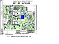
Quick Fix for M1146 & M1126
To speed up the servicing of the AP4020 or AP4040 on your bench, Yorkville
Sound’s service department has developed a method to replace the components most likely to fail when a M1146 amplifier board requires service.
This Quick Fix kit contains the procedure, assembly drawings, and components to perform the Quick Fix to a M1146 or M1126 board.
It should be understood that the person using this procedure knows how to
test resistors, diodes, and transistors to determine if they are defective. This procedure is not intended to be a substitute for one’s lack of electronic capability.
Before starting, look at the board for repair and locate the version number.
It is very important that you follow the procedure for the appropriate circuit
board version number.
A complimentary service manual for the AP4020 power amplifier is supplied with this M1146KIT.
STEP 1. Locate the assembly drawing for the version number printed
on the M1146 or M1126 circuit board to be serviced.
STEP 2. Remove all of the transistors coloured RED on the assembly drawing.
STEP 3. Measure and remove any of the diodes coloured BLUE on the
assembly drawing that may be damaged. Replace a 1N4732A 1W
4V7 zener (#6459) ZD12 along with a series 0.5 ohm R85 resistor.
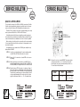
STEP 4. Rotate the trim pot RT1 fully counter - clockwise as in figure 1.
Inspect and replace any resistors that look burnt. Measure all of
the resistor values coloured YELLOW on the assembly drawing.
The value that you measure may not be exactly what is shown
on the assembly drawing but if the resistor doesn’t look damaged it should measure within + or – 5% of the printed value.
REAL Gear.
REAL People.
U.S.A.
Canada
Voice: (905) 837-8481
Fax: (905) 837-8746
Voice: (716) 297-2920
Fax: (716) 297-3689
Figure 1
STEP 5. Measure the resistor coloured GREEN. The measured value
should measure within + or – 5% value listed in the table
below. Replace any resistor that measured beyond the + or –
5% value listed in the table below.
RESISTOR
NUMBER
PRINTED
VALUE
R10
4K7
REAL Gear.
REAL People.
550 Granite Court
Pickering, Ontario
L1W-3Y8 CANADA
1
Yorkville Sound Inc.
4625 Witmer Industrial Estate
Niagara Falls, New York
14305 USA
-5%
3K08
3K25
+5%
3K41
U.S.A.
Canada
Voice: (905) 837-8481
Fax: (905) 837-8746
www.yorkville.com
Yorkville Sound
CORRECT
MEASURED VALUE
Voice: (716) 297-2920
Fax: (716) 297-3689
www.yorkville.com
Yorkville Sound
550 Granite Court
Pickering, Ontario
L1W-3Y8 CANADA
1
Yorkville Sound Inc.
4625 Witmer Industrial Estate
Niagara Falls, New York
14305 USA
SERVICE BULLETIN
SERVICE BULLETIN
AP4020 &
AP4040
AP4020 &
AP4040
STEP 6. Measure across the pair of test points shown in the component
layout listed in the table below. If the measured value is not
within + or – 10% of the value listed in the table then replace
the resistors shown in the table below.
TEST
POINTS
LAYOUT
REFERENCE
CORRECT
MEASURED VALUE
LAYOUT
REFERENCE
R10
4K7
-10%
+10%
15ohm 17ohm 19ohm
R11, R12, R14
STEP 7. Measure the resistors coloured ORANGE. Since the value of
these resistors is 0.1 ohm, your ohmmeter will measure the
higher series resistance of the test leads if the resistor is OK. If
the resistor is damaged your ohmmeter will read a very high
resistance (an open circuit). Replace any damaged resistors.
STEP 8. Measure the output TO–3 transistors (Q13 to Q28) to determine if any are damaged. Mark any damaged transistors with
a marking pen.
STEP 9. Replace any output transistors that you have marked as being
damaged. Replace any diodes that you have found to be damaged. Replace all of the red transistors that were removed.
STEP 10. Inspect the traces on the circuit board for any that have ‘fused’
open or looklike they got very hot. Bridge and solder a piece of
wire over any damaged traces.
AFTER YOU HAVE REPLACED ALL OF THE NECESSARY COMPONENTS INSPECT
THE REPAIRED BOARD FOR ANY MISSING PARTS, CORRECT VALUES IN THE CORRECT POSITION AND THAT ALL COMPONENTS ARE SOLDERED.
Testing Repaired Circuit Boards
Now that you have rebuilt the M1146 or M1126 circuit board. It is just as
important to properly power up the board. If the sinewave doesn’t look right
check the signal at test point (1) to ensure that the voltage amplifier isn’t distorting the signal. If there is still a damaged part on the board instantly turning it on could blow up the board and you would be back where you started.
Connect the power wires and ground to the power supply. Connect a digital multimeter to test pins 8 and 9 to measure the bias quiescent current
and place a scope probe on the speaker output. Be sure to turn the quiescent current trimpot RT1 fully counter clockwise.
Now using a variac slowly turn up the AC main voltage while monitoring
the quiescent voltage and the speaker output trace on the scope. Watching
these two test points is a good indicator of the health of the board. If you
have a second multimeter connect it up from the speaker output to test
point 4 or 5. As you variac up also check these DC battery voltages to
ensure that they both increase in voltage to approximately +12 or –12 vdc.
If the board looks OK after variacing up to 120vac then slowly turn up the
bias (RT1 trimpot) to obtain 3 to 5 millivolts of bias voltage on test points 8
and 9. Check the speaker output with a 1KHZ sinewave with no load. If this
looks good place the minimum rated load (4 Ohm for M1126, 2 Ohm for
M1146) on the speaker output and increase the sinewave amplitude to the
point of clipping. If the signal looks free of oscillation, place a short across
the speaker posts. The amplifier should go into protect mode after 1/10 of a
second. Remove the short and the sinewave will appear 6 seconds later.
Reassemble the complete amplifier and run just clipping music or pink
noise into the minimum rated speaker load for that model of amplifier. Let
the amplifier heat up for 20 minutes. This will check the thermal mounting of
the transistors and for any weak parts not caught during troubleshooting.
If the amplifier passes this test the product is ready to
return to the customer.
REAL Gear.
REAL People.
U.S.A.
Canada
Voice: (905) 837-8481
Fax: (905) 837-8746
Voice: (716) 297-2920
Fax: (716) 297-3689
REAL Gear.
REAL People.
Voice: (905) 837-8481
Fax: (905) 837-8746
www.yorkville.com
Yorkville Sound
550 Granite Court
Pickering, Ontario
L1W-3Y8 CANADA
2
Yorkville Sound Inc.
4625 Witmer Industrial Estate
Niagara Falls, New York
14305 USA
U.S.A.
Canada
Voice: (716) 297-2920
Fax: (716) 297-3689
www.yorkville.com
Yorkville Sound
550 Granite Court
Pickering, Ontario
L1W-3Y8 CANADA
2
Yorkville Sound Inc.
4625 Witmer Industrial Estate
Niagara Falls, New York
14305 USA
A
B
C
D
E
F
G
I
J
K
L
M
N
O
P
Q
1
D3
3V0
MINI
R36
1/4W
8M2
MINI
47K
1/4W
R27
FLMP
249R
1/8W
R21
LM13600N
U4:B
.
15K
1/4W
R26
5908
GRN
FLMP
3
LD2
{Function}
.
249R
1/8W
R22
0W5
1N5225B
MINI
C2
220P
TO92
.
1
100V
2
3
4
MINI
10K
AUD
4390
R45
1/4W
14K7
16V
R35
1/4W
78K7
.
6
.
C26
33U
P2
M Function
R136
1/4W
1K2
5
7
.
MC33078P
8
9
R44
1/4W
1K
U2:B
C38
220P
MINI
5
10
11
100V
12 W1:B
12 W1:C
12 W1:D
4
12 W1:E
12 W1:F
12 W1:G
12 W1:H
12 W1:I
12 W1:J
5
12 W1:K
12 W1:L
5908
GRN
EBC
TO-92
MINI
LD5
{Function}
4K7
1/4W
R63
.
15K
1/4W
R38
C40
100P
100V
C18
47P
FLMP
249R
1/8W
R37
LM13600N
U3:B
R65
22M
249R
1/8W
R60
LM13600N
U3:A
.
15K
1/4W
R55
8
(VCC)
100V
10K
AUD
4390
U2:C
P1
M Function
16V
R42
1/4W
78K7
.
V-
C25
33U
R40
1/4W
14K7
.
R41
1/4W
1K
100N
C5
63V
(VCC)
MC33078P
C37
220P
100N
C6
63V
U2:A
100V
LM13600N
U4:C
6745
Dual VCA
{Function}
LM13600N
U4:D
6745
Dual VCA
{Function}
100N
C8
63V
10
Product
6745_PC
AP-VX-VTC POT PCB
PCB# X8011
POT PCB
11
Sheet 1 of 1
Rev:8V00
Date: Fri May 29, 2009
Filename: X8011V800sch.sch2002
A
B
C
D
E
F
9
(VCC)
LM13600N
U3:C
6745
Dual VCA
{Function}
MINI
10
100N
C7
63V
(VCC)
LM13600N
U3:D
6745
Dual VCA
{Function}
4
6840_PC
V+
MINI
9
7
MINI
47K
1/4W
R64
FLMP
FLMP
D1
3V0
TO92
.
15K
1/4W
R62
.
249R
1/8W
R61
0W5
1N5225B
249R
1/8W
R58
Q1
5105
63V
U4:E
R46
1/4W
82K
FLMP
C21
220N
8
5906
RED
8
.
100K
1/4W
R2
MINI
*
47K
1/4W
R56
.
R3
1/4W
470K
R34
1/4W
7
C B E
TO-92
4K7
1/4W
R54
.
15K
1/4W
R59
TO92
MPSA13
MINI
R57
22M
100V
4148
MINI
U3:E
MINI
Q4
5102
C1
220P
.
BC560C
D9
1/4W
R8
1/4W
4K7
1/4W
R39
1/4W
15K
MINI
MINI
R30
1/4W
1K
.
63V
6
R5
1/4W
8M2
C4
470N
.
C10
470N
LD1
{Function}
MINI
R29
1/4W
620R
63V
BC560C
TO92
Q3
5102
R33
1/4W
10K
BC550C
BC560C
2N5401
2N5551
MPSA06
MPSA13
MPSA43
MPSA56
MPSA63
R32
1/4W
15K
6
C35
4U7
MINI
R31
1/4W
62K
63V
.
12
12 W1:A
.
100V
249R
1/8W
R23
LM13600N
U4:A
R15
22M
R1
1/4W
100K
.
15K
1/4W
R25
R55A
1/4W
220R
C17
47P
FLMP
2
R55B
1/4W
220R
4
C41
100P
FLMP
249R
1/8W
R24
Q2
5106
220N
C22
LD3
{Function}
W2
MPSA63
63V
LD4
{Function}
5906
RED
MINI
4K7
1/4W
R17
.
15K
1/4W
R20
47K
1/4W
R28
.
R4
1/4W
470K
100V
4K7
1/4W
R18
.
15K
1/4W
R19
*
MINI
R16
22M
5906
RED
TO92
R43
1/4W
82K
1/4W
MINI
5908
GRN
R47
1/4W
3604
Q5
5102
4148
MINI
1/4W
R50
1/4W
15K
.
3
D6
R7
1/4W
4K7
LD6
{Function}
2
MINI
BC560C
.
* NOTE:
M1128 - FOR R34 NAD R47 USE #4821 470R
M1133 - FOR R34 AND R47 USE #4808 2K
R53
1/4W
620R
C36
4U7
MINI
63V
R48
1/4W
10K
.
C9
470N
R52
1/4W
1K
R49
1/4W
15K
Q6
5102
C3
470N
MINI
0W5 D2
4V7
1N750ARL
R51
1/4W
62K
BC560C
TO92
63V
63V
1
H
G
H
I
J
K
L
M
N
O
P
Q
11
R42
78K7
14K7
C25
R58
R46
R40
16V
33U
LM13600N
249R
R38
22M
R65
100N
15K
249R
R61
C7
C8
100N
R60
47K
R64
X20
R59
R54
4K7
22M
249R
47K
249R
AUD
10K
BlankSize - 14000x11000
P1
LD2
R62
M1133-VTC
X8011
V800
M1128-AP-VX
X22
Channel B
15K
82K
X19
RSIG
LIMABLE
RSPOST
LSPRE
8M2
R56 R36
R37
R57
X21
GRN
C37
100P
C40
VV+
LSPOST
RREF
LREF
R63 5908
R Clip
R Activity
MC33078P
C18
47P
+
15K
U3
47K
X18
15K
U4
100P
C41 Q4
R44 BC560C
1K
220P
C38
U2
-
RED
MPSA63
620R
C4
220R
R55A
C35
14K7
R45
82K
R55B R43
78K7
R35
47P
C17
X16
RSPRE
W2
5906
62K
C2
X23
Q2 LD5 C22
R29R31 D3
3V0
220P
4K7
AUD
R33
R34
220N
Q3
R8
4K7
470N
BC560C
470K
220P
1K
R41
R55
15K
220R
10K
R19
R23
249R
R24
249R
R4
63V
4U7
P2
LM13600N
4148
D2
R32
10K
X6
470K
R3
C26
22M
R18
22M
R16
BRPRTCT
Channel A
R25
4K7
D9
15K
470R
470N
220N
C21
5906
5908
L Clip
L Activity
BC560C
X11
R28
SHORT AXIS
C5
4K7
100N
100N
C3
470N
R17
MPSA13
5906
GRN
-
C6
62K
15K
Protect
Power
+
C36
1K
R51
-
-
63V
4U7
X10
D1
R22
LD1
249R
R21
249R
R52
R26
R27
47K
15K
R20
15K
R15
620R
R53
LD6
GRN
+
+
5908
Q5
4148
-
R136
1K2
D6
Q1
+
LD4
RED
8M2
R5
C10
R30
1K
4V7
3V0
X8
REDLD3
100K
220P
R47
470R
X15
R2
C1
R39
X14
21in 14C
3604
X13
X1
15K
R50
100K
X9
To Power Supply Pcb
X4
16V
33U
R7
R1
12
2329
15K
4K7
470N
C9
6
R48
10K
X12
V+
1
15K
Q6
BC560C
V-
LREF
RREF
RSIG
ACT
PRTCT
W1
R49
LCLP
X24
-
RCLP LVGND
AP-VX
VTC
X17
+
M1128
M1133
LSPOST
M1128 AP-VX
CLINCH
ORIGIN
INSERT
VCD
ORIGIN
LONG AXIS
StepAndRepeat - [email protected]@3.300
SEE LAYOUT DOCUMENTATION
SEE LAYOUT DIAGRAM
X8011 PRODUCTION NOTES - M1128 AP/VX
1.
P22
POT
PCB 3511
WASHER 8870
SCREW
0.4"
2.
LED
SPACER
PT#3739
SEE LAYOUT DIAGRAM
X8011 DRILL HISTORY
X8011 PCB_DATABASE_HISTORY
MODEL(S):-
AP4020 AND AP4040/VX2400 AND VX2402/V42 AND V44
# DATE
VER# DESCRIPTION OF CHANGE
1 OCT/97
1.00
FIRST PRODUCTION
2 APR/17/98
2.00
#5664 RIBBON CABLE CONNECTIONS CHANGED FOR
3 .
.
PROTECT CIRCUIT
4 DEC/09/98
3.00
PC#5736 TRACES CHANGED POT SUPPORT SCREWS
5 .
.
ADDED
6 NOV/20/01
3.10
PC#6466 LD7,LD8 NSL28AA->NSL32SR2
7 JUL/09/02
4.00
PC#6401 PARTS MOVED NEAR P2
8 OCT/25/02
4.10
PC#6568 R44/R41 10K->1K
9 APR/15/05
5.00
PC#6873 REDO SOLDERMASK
10 JUN/05/06
6.00
PC#7138:GT:CONVERT TO PCAD2002. CHANGE OPTO
11 .
.
LIMITER TO 13600 #6745 LIMITERS FOR ROHS
12 .
.
REPLACE C3,C4,C9 AND C10 WITH #5234 470N 63V
13 .
.
REPLACE R31 AND R51 WITH #6139 62K 1/4W
1 .
.
REPLACE R4 WITH #6127 470K 1/4W
7.00
Removed shear, solder update, std board size
2 JUN/23/08
CREATE X8011, M1128 FOR AP, VX AND M1133 FOR VTC
3 28-MAY-2009 8.00
.
PC#7717, 7718 - M1133,V42 AND V44 CHANGE R34
4 .
.
AND R47 FROM 470R TO 2K #4808
5 .
6 D
V
N
7 D
V
N
8 D
V
N
9 D
V
N
10 D
V
N
11 D
V
N
12 D
V
N
13 D
V
N
MODEL(S):#
1
2
3
4
5
6
DATE
D
D
D
D
D
D
MODEL(S):#
1
2
3
4
5
6
PC#
PC
PC
PC
PC
PC
PC
AP4020 AND AP4040/VX2400 AND VX2402/V42 AND V44
VER# DESCRIPTION OF CHANGE
V
N
V
N
N
V
N
V
V
N
N
V
X8011 PENDING CHANGES
AP4020 AND AP4040/VX2400 AND VX2402/V42 AND V44
PENDING CHANGE
X
X
X
X
X
X
LEAD/PIN REFERENCE
BC550C
BC560C
2N5401
2N5551
MPSA06
MPSA13
MPSA43
MPSA56
MPSA63
*PLACE IMPLEMENTED CHANGES INTO BOARD HISTORY
C B E
TO-92
EBC
TO-92
A
B
C
D
E
F
G
H
I
J
K
L
M
N
O
P
Q
R
S
T
U
V
1
1
2
D7
4148
2
C23
33U
U3:A
16V
MC33078P
R
T
-
-
-
C29
150N 63V
S1:B
4
MC33078P
0.1%
LIMITER
0.1%
5
S2:A
MONO-STEREO-BRIDGED
S3:A
S3:B
3705
L
3705 MONO-STEREO-BRIDGED
M
COM
3570
C10
220P 100V
R24
1/4W
9K76
R26
1/4W
9K76
W1
R20
1/4W
120K
.
R6
1/4W
33K
.
S
FILTER SW
S2:B
J3
C30
150N 63V
U4:A
R25
1/4W
1K54
.
5
3
C33
68N 100V
3436
LIMITER
4
C34
68N 100V
0.1%
R109B
1/4W
4M7
LINE XLR
R23
1/4W
9K76
0.1%
R10
1/4W
56K
.
J1
R22
1/4W
9K76
C12
C11
220P 100V 220P 100V
R27
1/4W
1K54
.
R28
1/4W
56K
.
C9
220P 100V
3
L
R
M
COM
R
6
6
S3:C
S3:D
3705 MONO-STEREO-BRIDGED
L
COM
M
R111
1/4W
10R
RAD
R112
1/8W
10R
.
3705 MONO-STEREO-BRIDGED
L
R
COM
M
MC33078P
R
U1:B
7
7
R37
R38
10K0
.
10K0
.
1/4W
1/4W
8
10
R16
1/4W
9K76
0.1%
0.1%
Copper
Tie Here
FILTER SW
U4:B
C28
150N 63V
S1:A
MC33078P
11
R18
1/4W
120K
.
12
GND LIFT
C1
22N 275V
M1129 Database History
C14
100N 100V
Copper
Tie Here
C27
150N 63V
0.1%
S4:A
Tie-net Name
10
C32
68N 100V
R14
1/4W
9K76
0.1%
C13
100N 100V
12
100V 220P
C7
R12
1/4W
9K76
R11
1/4W
1K54
.
11
C31
68N 100V
U1:A
C5
220P 100V
J2
U3:B
MC33078P
3657_OBS
9
16V
MC33078P
D4
R13
1/4W
1K54
.
C24
33U
100V 220P
C8
R15
1/4W
9K76
4148
T
R109A
1/4W
4M7
R
R9
1/4W
56K
.
S
R19
1/4W
56K
.
J4
S4:B
9
C6
220P 100V
8
13
8
V+
8
V+
U3:C
4
V-
V-
U4:C
MODEL(S):-
C16
100N 50V
15
AP2020 AP4020 AP4040 AM1CE
VER# DESCRIPTION OF CHANGE
# DATE
1.00
FIRST PRODUCTION
1 OCT/97
2.00
SWITCH NETS RREF WITH LREF AND RSPRE WITH
2 NOV/97
.
LSPRE AT 14 PIN CONNECTOR. INPUT TO NONINVERTING
3 .
CHANGE C27, C29, C28, C30 TO 150N
.
4 DEC/02/97
PC#5694 PINS 10-12 OF MC2 CONNECTED TO BRG SWT
3.00
5 APR/16/98
ISOLATE PIN OF S3
4.00
6 JUL/01/98
4.10
PC#6436 REPLACE R119 (10K0) WITH JUMPER X119
7 SEP/06/01
5.00
PC#6873 REDO SOLDERMASK
8 APR/15/05
CONVERT TO PCAD2002, PC#6944:ROUTE GAUGE,
6.00
9 JUL/2005
PC#6914:ADD TARGETS
10 AUG-15-2005 .
V
N
11 D
V
N
12 D
V
N
13 D
#
1
2
3
4
5
6
7
8
9
10
11
12
13
16
AP4020 / AP4040 / AP2020 / AM1CE
VER# DESCRIPTION OF CHANGE
1.00
FIRST PRODUCTION
2.00
REVERSED INPUT POLARITY. MODIFIED FOR AP2020
.
C27, C28, C29, C30 TO 150n
2.10
PC#5694 ADD NETS BRPRTCT, LVGND-28 TO BRG SW
2.20
DELETE R119
3.00
CONVERT TO PCAD2002
V
N
V
N
V
N
V
N
V
N
V
N
V
N
DATE
OCT/1997
NOV/12/97
DEC/02/97
APR/22/98
SEP/06/01
JUL/2005
D
D
D
D
D
D
D
Product
PCB# M1129
Date: Tue May 02, 2006
Filename: M1129-6v00.sch2002
B
C
D
E
F
G
H
I
J
K
L
M
N
O
P
Q
R
S
15
16
{Drawing Number}
{Title}
17
A
14
M1129.sch_schematic-DATABASE_HISTORY
C15
100N 50V
4
V-
U1:C
4
V+
14
C39
100N 100V
MODEL(S):-
8
13
T
U
Sheet 1 of 2
Rev: v6.00
V
17
3705
S2
S1
W2
3417
X50
S3
X43
AC AM AR BL
AL
CC CM CR DL
CL
3436
RT
V
X42
9K76
220P
100N
220P
220P
X33
TIP-SW
TIP-SW
-
J3
TIP
TIP
BEC
RING-SW
-
7
RING-SW
-
3657
3657
LONG AXIS
SL-SW
VCD
ORIGIN
-
INSERT
SLEEVE
7
RING
SHORT AXIS
RING
SL-SW
SLEEVE
CLINCH
LOC
X18
LINE_IN
X34
J4
ORIGIN
V6.00
M1129
R23
C9
C16
C12
C11
R25
1K54
1K54
R27
LEFT
X17
1K54
R13
LINE XLR J1
9K76
9K76
X16
J2
X19
X37
R24
X119
C15
100N
C39
220P
220P
C6
56K
120K
R20
MC33078P
X23
X24
X25
10K0
R37
MC33078P
9K76
220P
C10
X32
X15
R22
R16
9K76
220P
100N
X22
RREF
X26
LREF
X27
X28
220P
C7
9K76
C5 C8
R12
9K76
R15
U4
TP1
TP4
U1
C34 C30
X36
R26
LSPOST
V-
X13
10K0
TP3
R11
1K54
4148
D7
X35
R38
R14
9K76
MC33078P
68N
7
X29
14
T P2
V+
13
X20
6
X38
X30
12
56K
5
11
R28
4
10
X11
X12
X40
R10
3
U3
9
C33
D4
RSPRE
14 PIN SCKT
8
C29
150N
68N
R19
4148
X41
LSPRE
R109B
4M7
R18
16V
33U
33U
2
RSPOST
LIMABLE
RSIG
X39
C23
16V
1
W1
FROM POTS
C31
68N
C24
TP5
100N
C14
56K
56K
R9
X10
C13
100N
RIGHT
68N
C32
150N
R111
10R
R109A
4M7
C27
X9
W3
X31
R6
FILTER SW
33K
3436
LINE_IN
150N
120K
W4
C28
R112
LIMITER
275V
22N 6435
GND LIFT
10R
150N
BC BM BR
DC DM DR
3436
BRIDGED - STEREO - MONO
C1
AP2020 / AP4020 /
AP4040
S4
M1129.sch_schematic-DATABASE_HISTORY
MODEL(S):#
1
2
3
4
5
6
7
8
9
10
11
12
13
DATE
OCT/1997
NOV/12/97
DEC/02/97
APR/22/98
SEP/06/01
JUL/2005
D
D
D
D
D
D
D
AP4020 / AP4040 / AP2020 / AM1CE
VER# DESCRIPTION OF CHANGE
FIRST PRODUCTION
1.00
REVERSED INPUT POLARITY. MODIFIED FOR AP2020
2.00
.
C27, C28, C29, C30 TO 150n
PC#5694 ADD NETS BRPRTCT, LVGND-28 TO BRG SW
2.10
DELETE R119
2.20
3.00
CONVERT TO PCAD2002
N
V
N
V
V
N
V
N
V
N
V
N
V
N
M1129 Database History
MODEL(S):-
AP2020 AP4020 AP4040 AM1CE
VER# DESCRIPTION OF CHANGE
# DATE
1 OCT/97
1.00
FIRST PRODUCTION
2 NOV/97
2.00
SWITCH NETS RREF WITH LREF AND RSPRE WITH
3 .
.
LSPRE AT 14 PIN CONNECTOR. INPUT TO NONINVERTING
4 DEC/02/97
.
CHANGE C27, C29, C28, C30 TO 150N
5 APR/16/98
3.00
PC#5694 PINS 10-12 OF MC2 CONNECTED TO BRG SWT
6 JUL/01/98
4.00
ISOLATE PIN OF S3
7 SEP/06/01
4.10
PC#6436 REPLACE R119 (10K0) WITH JUMPER X119
8 APR/15/05
5.00
PC#6873 REDO SOLDERMASK
9 JUL/2005
6.00
CONVERT TO PCAD2002, PC#6944:ROUTE GAUGE,
10 AUG-15-2005 .
PC#6914:ADD TARGETS
V
11 D
N
12 D
V
N
13 D
V
N
M1129 PENDING CHANGES
MODEL(S):#
1
2
3
4
5
6
PC#
PC
PC
PC
PC
PC
PC
AP2020/AP4020/AP4040/AM1CE
PENDING CHANGE
X
X
X
X
X
X
*PLACE IMPLEMENTED CHANGES INTO BOARD HISTORY
M1129 DRILL HISTORY
MODEL(S):-
AP2020/AP4020/AP4040/AM1CE
# DATE
VER# DESCRIPTION OF CHANGE
1 APR-03-2003 V06
N
2 AUG-15-2005 V07
CONVERT TO PCAD2002
3 D
V
N
4 D
V
N
5 D
V
N
6 D
V
N
M1129 PRODUCTION NOTES
1 FOR XLR #3657 USE SCREW PT#8829
UP THROUGH THE BOTTOM
2 FOR M1129B VX1200/2400/J/2402
DO NOT STUFF X40 AND X41
ADD WIRES IN BOARD ASSEMBLY
A
B
C
D
E
F
G
H
I
J
K
L
M
N
O
P
Q
R
S
T
U
V
1
1
6880
4N35
6880
4N35
6
1
MINI
R89
1/4W
220K
U1:B
U1:A
5
R80
1/4W
220R
2
4
ZD10
4V7
0W5
1N750ARL
R30
1/4W
620R
C9
4N7
R31
1/4W
39R
250V
.
R59A
1/4W
10R
R60
5.0W
0R1
.
.
R58
5.0W
0R1
.
.
R56
5.0W
0R1
R53
5.0W
0R15
.
R62
2.0W
3R9
250V
.
.
.
R61
5.0W
0R1
R59
5.0W
0R1
R57
5.0W
0R1
R52
5.0W
0R15
C19
10N
.
MJ21195
Q22
6910
TO3
{Function}
MJ21195
Q24
6910
TO3
{Function}
MJ21195
Q26
6910
TO3
{Function}
MJ21195
Q28
6910
TO3
{Function}
D17
D18
D19
MR854
MR854
MR854
D16
.
9
R48
1/4W
39R0
FUSIBLE
MR854
MJ21195
Q25
6910
TO3
{Function}
MJ21195
Q27
6910
TO3
{Function}
10
R64
1/4W
33K
.
.
MINI
R88
1/4W
220K
C16
470P
100V
R81
0W5
1/4W
1N750ARL
220R
1
U2:A
C21
10U
6880
4N35
5
D31
6880
4N35
U2:B
4007
.
MBS4992
R47
1/4W
39R
400V
MR854
16V
D
C15
2N2
MTP8P20
Q12
6925
TO220
Function
ZD11
4V7
MINI
2
4
Q29:A
5190
{Voltage}
TO92
S
P
G
.
R45
5.0W
3K6
D20
MT2
MJ21195
Q23
6910
TO3
{Function}
Q30
R86
1/4W
470R
MJ21195
Q21
6910
TO3
{Function}
ZD9
16V0
MT1
STM-BTB-600BRG
1W0
1N4745A
R54
5.0W
3K6
Function 6517
G
TO220
200V
220P
C17
50V
C5
22U
MINI
R18
1/4W
10K0
R17
1/4W
151R
.
D10
MINI
R40
1/4W
1K
8
100V
Q4
5101
FUSIBLE
7
R50
1/4W
270R
R44
1/2W
1R
250V
6
L1
FLMP
C31
22N
MINI
R68
1/2W
22K
.
D11
D7
D9
4148
.
MINI
R42
1/4W
4K7
.
FLMP
C14
220N
3820
R51
1/8W
220R0
R43
1/4W
470R
100V
BAV21
4148
.
R27
1/4W
2R2
0W5
1N5246B
R41
1/4W
2R2
63V
.
R39
1/4W
91K
.
11
R65
1/4W
10R
.
.
.
R67
1/2W
22K
12
R66
1/2W
22K
80V
C24
4700U
80V
C25
4700U
5
.
R49
1.0W
1R
C23
4700U
C28
4700U
3628
SPEAKON 4C
Function
J2:B
MINI
MINI
ZD7
16V0
.
C8
1U
MINI
R23
1/4W
4K7
D5
4148
C13
22N
6
80V
2_
2+
R63
5.0W
5R6
R38
1/4W
27K
TO92
R46
1/4W
1K
C27
4700U
80V
C26
4700U
1+
1_
4UH
Q10
5102
MINI
12
MR854
MJ21196
Q20
6909
TO3
{Function}
R35
1/4W
1K
R25
1/4W
220K
R21
1/4W
2K2
0W5
1N5242B
ZD5
12V0
TO92
BC560C
80V
80V
11
MJ21196
Q18
6909
TO3
{Function}
.
MINI
MINI
.
R37
1/4W
27K
20K0
1/4W
R40B
Q8
5101
R22
1/4W
3K
R13
1/4W
43K
.
.
MINI
4148
50V
C4
470P
R36
1/4W
91K
R35A
1/4W
20K0
BC550C
MINI
0W5
1N5242B
C7
330U
0W5
1N750ARL
.
R14
1/4W
39R
ZD4
12V0
25V
C6
330U
25V
FLMP
R85
1.0W
0R47
ZD12
4V7
FLMP
FLMP
R83
1/4W
200R0
FLMP
R12
1/8W
39R
R11
1/4W
22R
MINI
MINI
R16
1/4W
12K
R15
1/4W
150R
BC550C
80V
R69
1/2W
22K
D30
R32
1/4W
39R0
MINI
R20
1/4W
3K
.
MINI
R8
1/4W
12K
R7
1/4W
150R
R10
1/4W
4K7
.
R4
1/4W
2R2
R70
1/4W
18K
2SA2121-0
Q6
7004
TO3P
{Function}
MJE350
Q41
6874
TO126
MJ21196
Q16
6909
TO3
{Function}
4
J2:A
Function
SPEAKON 4C
3628
D15
FLMP
BAV21
470R
1/4W
R87
MINI
50V
C2
1N
.
R3
1/4W
2R2
FUSIBLE
.
200V
C1
1N5
R65A
1/4W
10R
FUSIBLE
63V
FUSIBLE
50V
C3
22U
MINI
R6
1/4W
10K0
R5
1/4W
151R
FUSIBLE
330U
C29A
25V
R66A
1/4W
10R
160V
R61A
1/4W
47R0
R62A
1/4W
47R0
FUSIBLE
R64A
1/4W
151R
FUSIBLE
C25A
4U7
MINI
R70A
1/4W
10K
16V
FLMP
R71A
1/8W
33R
MINI
TO92
4148
FLMP
D22
MR854
R55
1/8W
220R0
MINI
C22
4700U
80V
C29
4700U
.
R24
1/4W
220K
Q7
6854
D4
R84
1/4W
200R0
D13
MR854
MINI
TO92
D3
TO92
R74
1/4W
330R
.
.
R19
1/8W
249R
TO92
Q31
R73
1/4W
2K
R72
1.0W
4K7
63V
TO-92
6478 {Watts}
VCC {Function}
AS35FNOUT
GND
Q21A
5102
TO92
R34
1/4W
270R
100V
Q9
5101
2N6517
FLMP
BC560C
TO92
C31A
33U
MINI
R53A
1/4W
2K
Q17A
5101
C30
22N
MINI
10K
Lin
4520
BC560C
MR854
MJ21196
Q14
6909
TO3
{Function}
MR854
MJ21196
Q19
6909
TO3
{Function}
MJ21196
Q17
6909
TO3
{Function}
BC550C
R9
1/8W
249R
Q2
5102
C28A
10U
.
R69A
1/4W
3K3
MINI
R51A
1/4W
1K5
500V
.
C23A
10P
BC550C
R26
1/4W
470R
100V
D1
FLMP
160V
R63A
1/4W
39R0
FUSIBLE
MINI
R50A
1/4W
4K7
.
R42A
1/4W
56K
D18A
C12
22N
MJ21196
Q15
6909
TO3
{Function}
D14
FLMP
4148
D2
RT1
M BIAS TRIM
R28
1/2W
1R
.
R82
1/4W
200R0
TO92
1W0
1N4745A
250V
3628
SPEAKON 4C
Function
J1:B
D21
MJ21196
Q13
6909
TO3
{Function}
R33
1.0W
1R
2SC5949-0
Q5
7005
TO3P
4148
R2
1/4W
68R
4148
D21A
MINI
4148
D15A
1K
1/4W
R45A
.
MJE340
Q16A
6873
TO126
TO92
R41A
1/4W
7K5
4148
Q13A
5114
9
BC550C
.
MJE350
Q19A
6874
TO126
MPSA92
C11
220N
Q1
5101
FUSIBLE
10MM
R60A
2.0W
220K
D23A
ZD8
16V0
R29A
5.0W
3K6
{Function}
MJE340
Q40
6873
TO126
4148
4148
8
ZD13
33V0
63V
MINI
FUSIBLE
R58A
1/4W
39R0
4148
4148
MINI
R43A
1/4W
3K
MINI
D16A
50V
MINI
400V
S
.
BC560C
4148
D20A
C20A
2N2
MINI
C19A
22U
R44A
1/4W
1K
4148
D14A
R40A
1/4W
220R
R71
1/4W
100K
D19A
TO92
.
3
2+
IRF630NPBF
Q11
6752
TO220
Function
N
G
FLMP
.
MJE340
Q18A
6873
TO126
Q12A
5113
R56A
1/4W
17K8
220P
C18
TO92
R1
1/4W
39R0
MPSA42
D13A
C18A
22U
4148
50V
.
R39A
1/4W
7K5
MINI
R46A
1/4W
4K7
.
MJE350
Q15A
6874
TO126
D17A
D22A
6
7
R68A
1/4W
3K3
TO92
4148
5
200V
Q3
5102
C27A
10U
500V
.
R38A
1/4W
56K
.
C22A
10P
MINI
R47A
1/4W
1K5
R55A
1/4W
21K5
W1:A 8
TO92
Q14A
5102
MINI
W1:B 8
0W5
1N5257B
1+
2_
.
FUSIBLE
BC560C
R205
1/4W
47K
W1:C 8
C32
10U
FUSIBLE
MINI
R57A
1/4W
151R
FUSIBLE
Q20A
5101
.
4
10
400V
.
R29
5.0W
3K6
C26A
4U7
R49A
1/4W
2K
FLMP
W1:E 8
W1:D 8
BC550C
R72A
1/8W
33R
W1:F 8
.
1_
C30A
33U
W1:G
8
.
D
R67A
1/4W
10K
W1:H 8
2
.
RED EY2
J1:A
Function
SPEAKON 4C
3628
C10
2N2
16V
3
.
BLK EY1
MINI
4007
2
13
BC550C
BC560C
2N5401
2N5551
2N6517
MPSA13
MPSA43
MPSA56
MPSA63
YS6909
13
AS35
MBS4942
M1146 Database History
EBC
TO-92
#
1
2
3
4
5
6
7
8
9
10
11
12
13
1
2
3
4
5
6
7
8
9
10
11
12
13
BOTTOM
VIEW
IN
OUT
REF
MT2
N/C
MT1
C B E
TO-92
MODEL(S):-
E
B
14
MJL21194
MJL1302A
MJL3281A
MJL21193
2SA2121-0
2SC5949-0
15
STM-BTB-600BRG
G D S
B
C
E
MT1
MT2
G
16
E CB
AP4040
DATE
VER# DESCRIPTION OF CHANGE
FEB/12/98
DERIVED FROM M1126
1.00
JUN/19/98
1.10
PC#5767 C10,C15,C20A 2N2 TO PT#5427
JUL/4/98
1.20
PC#5798 R72 4K7 1/2W TO 4K7 1W
SEP/10/98
2.00
PC#5806 ADD 33R, 33u/16V ACROSS R57A,R64A,C30A,
.
.
-R72A,C31A,R71A
JAN/27/99
3.00
PC#5908 U1,U2 4N35 TO TLP621
JUL/08/99
4.00
SPKON JACKS RE-CONFIGURED
AUG/12/99
5.00
CORRECT ERROR IN SPKONS
OCT/12/00
6.00
PC#6278 ADD R86,C17 AT Q41. PC#6083 REDO GND TRA
AUG/28/01
7.00
PC#6429 ADD R87,C18 AT Q40
SEP/18/01
8.00
PC#6438 ADD R88,R89 AT U1, U2
MAY/03/02
8.10
PC#6517 Q13->20 #6900->#6909. Q21-Q28 #6927->#6910
.
.
R13 27K-<43K,C18 1N->220P,R87 100R->470R
PC#6607 C10,C15, C20A #5427->#5208
MAY/16/03
8.20
FEB/09/04NOV8.30
PC#6658 CHANGE BREAKAWAY AND ROUTE
SEP/2004
9.00
CONVERT TO PCAD2002
PC#7007 MAC-224-4 TO STM-BTB-600BRG
APR/25/06
9.10
MAY/02/06
9.20
PC#7083 MTP10N15L TO IRF630NPBF
APR/03/07
9.30
HA, PC#7076, REPLACE Q5 #6989 WITH #7004
Q6 #6990 WITH #7005
.
.
10.00 Solder Updates
NOV-19-08
D
V
N
N
V
D
D
V
N
D
V
N
N
V
D
14
15
16
Product
BCE
POWER AMP
AP4040
17
PCB# M1146
Sheet 1 of 1
Date: Thu Sep 25, 2008
Rev:v1000
Filename: M1146v1000p0sch.sch2002
A
B
C
D
E
F
G
H
I
J
K
L
M
N
O
P
Q
R
S
T
U
V
17
INSERT
SOCKET
ETCH
GUIDE
SOCKET WITH DIRECTION
TAB
CLINCH
SOCKET UPSIDE DOWN
MPSA42
Q12A
R57A
R72A
2K
151R
33R
C26A
Q20A
R49A
33U
16V
C30A
ORIGIN
VCD
LONG AXIS
AP4040 / V44 LAYOUT
SEE LAYOUT DOCUMENTATION
C29A
SIG
GND
CLIM
C8
Q7
2N6517
RED 2.5"
NFB
TSENSE
RED 13"
PRTCT
BLK 4"
BLK 14"
BLK
RED
EY2
RED 1BLK
3628 NL4MP-1
GND
SPEAKON 4C
1+
1+
J2
1-
2+
22-
2+
EY7
YEL
2.5"
ETCH
GUIDE
BLK
EY3
22N
AP4040/V44
Q10
EY8 J1
M1146
v10.00
YEL YEL
EY4
YEL
19"
DO NOT STUFF WIRES OR SPEAKON
JACKS FOR SERVICE BOARDS.
AP4040/V44
220R0
12+
3628
NL4MP-1
2+
22N
C30
2R2
R4
R3
R10
X21
39R0
4K7
MR854
TP9
R1
68R
R33
R39
X17
R85
D18
X8
R12
39R
0R47
1.0W
2R2
R14
R9
Body
C31 ZD12
R2
220R0
270R
4V7
39R
X16
91K
BAV21
249R
19
MJ21
R51
4148
Q40
470R
Q25
R55
D4
1R
1.0W
1R
1.0W
5
R43
BC560C
R49
7005
2SC5949-0
22R
D10
1K
27K
TO3P
R27 C13 R40
R41
22N R11
4148
R52
5
BC560C
5.0W
0R15
MJ
21
19
Q1
BC550C
R53
6
5.0W
0R15
Bo
dy
Q1
4
Body
196
MJ21
ETCH
GUIDE
MR854
Q13
X24
Q2
Q21
D16
5
Body
BLK
SPEAKON 4C
1+
11+
22-
BlankSize - 15000x11000
StepAndRepeat - [email protected]@0.000
ClinchRepeats - [email protected]@0.000
Q2
2
Bo
dy
MJ
21
19
Q19
1N5
D9
R60
196
MJ21
C1
50V
22U
R38
220P
X7
R59
5.0W
0R1
Bo
dy
D14
2R2
C12
20K0
C18
4148
B
0R1
5
5.0W
MJ
21
19
Q2
0
Body
TP8
C7
2R2
R40B
D1
E
Q2
6
Bo
dy
MJ
21
19
6
MR854
X32
R13
22N
470R
Q5
470R
R87
BC550C
12V0
C
TO3P
Q9
ZD5
1K
C3
C6
R26
43K
200R0
R82
X26
.
TO126
R35
C5
22U
50V
Q3
X37
R5
151R
R6
10K0
R8
12K
X15
150R
R7
1N
C2
D2
4148
7004
2SA2121-0
3K
25V
330U
Q6
200R0
R83
BC550C BC560C
12V0
TO220
Q4
B
.
TO126
X38
E
Q41
R84
200R0
C
6874
MJE350
R20
63V
1U
18K
6925
MTP8P20
330U
25V
470P
C17 220P
X22
39R0
X36
Q31
AS35FN
TO-92
MR854
R24
C4
20K0
R48
R37
D7
470R
R86
R15
Q8
150R
BC550C
12K
4K7
R16
249R
D5 R19
4K7
4148
D3
4148
R18
R22
3K
X23
10K0
ZD7 16V0
151R
R17
220K
220K
R25
R42
R35A
X30
27K
4148
ZD11
C16
X20
470P
16V0
39R
R74
330R
19
MJ21
R23
R70
4V7
R36
ZD9
R44 R47
1R
1/2W
ZD10
4007
X2
R73
2K
X10
BEC
X12
ZD4
X13
2K2
X14
R89
91K
BAV21
220K
4V7
R80
220R
C15
R58
Q17
EY5
W1
47K
R205
R21
X11
4N35
6880
1
6874
4007
220R
2328
D23A
D30
R81
X19
21K5
Q19A
MJE350
U1
47R0
4148
R63A
ZD13
R62A
6873
MJE340
Q18A
D19A
U2
39R0
4N35
6880
4148
33V0
R67A
R61A
47R0
D22A
4148
D20A
4148
D21A
4148
3K6
5.0W
2N2
BLU
5.0W
0R1
Bo
dy
196
MJ21
EY1
4U7
63V
Q12
8
C25A
R54
5.0W
W11
6
D15
CLIP
63V
4U7
C32
1K
YEL
220K
10U
63V
X1
R46
R45
Q11
R88
1.0W
4K7
5
10K
R72
R32 IRF630NPBF
R31
R68A
3K3
X4
.
R60A
THIS CAP IS
USED AS A
6873 SPACER
XC38
3K6
R61
5.0W
0R1
MJ
21
19
5
Q1
8
R56
5.0W
0R1
Bo
dy
Body
EY6
R71A
220N
250V
Q2
8
Bo
dy
MJ
21
19
6
MR854
R66A
10R
R55A
Q16A
MJE340
10P
C23A
22N
5882
Body
330U
25V
R58A
39R0
5882
LOC
BC550C
Q15A
MJE350
10P
C22A
C11
W9
C14
C25
220K
2.0W
6874 .
D19
Q21A
W10
R70A
R69A
BLU 6in
-145V
33R
10K
3K3
WC7
39R0
TO220
33U
16V
1R
1/2W
Q27
BC560C
R28
6752
220N
250V
C26
X9
R62
R53A
16V0
C10
2K
C20A
ZD8
C9
39R
19
MJ21
5.0W
4N7
Body
3K6
2N2
5.0W
3K6
D21
MR854
151R
C31A
10R
620R
D17
R64A
D14A
R29A
R29
R30
R57
5.0W
0R1
MJ
21
19
5
Q1
6
Q15
R65A
-78V
RT
V
RT
V
C27
R40A
WHT 7in
RT
V 4700U
80V
5896
D20
MR854
Q23
220R
R71
MR854
5
2N2
100K
D15A
50V
22U
C19A
D16A
4148
D13A
4148
4148
4148
R44A
1K
17K8
1K
R56A 10U
R45A
MPSA92
160V
Q13A R50A
4K7
C28A
4K7
R46A
D17A
4148
BC560C
Q14A
1K5
R47A
D18A
4148
BC550C
Q17A
1K5
R51A
NORMAL LARGE
R38A
R64
R65
Q2
4
Bo
dy
MJ
21
19
D22
160V
10U
3K
56K
W4
BLK 8in
R43A
NORMAL
C24
50V
22U
GND
EY10
3R9
2.0W
7K5
10N
5834
C19
BLU
33K
10R
TO220
6517
MR854
R39A
C28
4700U
80V
T
5896 R V
RT
V
MBS4992
Q29
C27A
YEL 10in
10U C21
16V
R42A
56K
C23
C18A
+78V
RT
V
+145V
RT
V
W8
TO92
4700U
80V
5896
RT
V
C22
4700U
80V
5896
+
W5
7K5
Pcb Mech M1146 v10.00
Top Assy M1146 v10.00
_
R59A
W7
X6
X5
C29
5896
1/2W
22K
1/2W
22K
RT
V
R67
RT
V 589
6
RT
V
R66
R41A
10R
X3
ORIGIN
1/2W
22K
1/2W
22K
4700U
RT
V 80V
RED 12in
470
0
80V U
STM-BTB-600BRG Q30
0W
5.
6
5R
W6
RT
V
19
MJ21
H
4U
58
96
63
R68
RT
V
MR854
L1
SHORT AXIS
Body
.
196
MJ21
.
D13
20
R69
4700U
80V
RT
V 5896
R
38
47
0
RT
V 80 0U
V
ETCH
GUIDE
INTO WAVE
YEL
EY9
6873
MJE340
X18
BIAS TRIM
RT1
10K
270R
R34
M1146
v10.00
BLK 3.5"
BLK 18"
ETCH
GUIDE
SEE LAYOUT DIAGRAM
M1146 - AP4040 / V44 PRODUCTION NOTES
4. MOUNTING HARDWARE FOR Q11,Q12
1. MOUNTING DETAILS FOR 5W ADD #8629 SPACERS ONLY ON
5 WATT RESISTORS R29 AND R45. ENSURE SPACERS ARE UNDER
RESISTOR BODY ENOUGH TO RAISE IT OFF THE BOARD SURFACE.
#8741 4-40X 1/2" BOLT
8. TAB WIRE COLOURS:
#3501 BELL WASHER
2. MOUNTING HARDWARE FOR Q5 AND Q6.
#8667 SHOULDER WASHER
T-220 DEVICE
TAB 1 RED 16AWG TAB 2 YEL 16AWG
TAB 3 BLK 16AWG TAB 4 WHT 16AWG
TAB 5 BLU 16AWG TAB 6 OUTPUT +
TAB 7 OUTPUT -
#3846 MICA
#8902 - 4-40 X 3/4 PAN PHIL
HEATSPREADER
#8485 ZINC #6 WASHER
PCB
#8701 4-40 KEPS NUT
Z234 CLAMP
T264 DEVICE
5. MOUNTING HARDWARE FOR TO3 OUTPUTS
#3797 THERMO PAD
HEATSPREADER
9. Q31 IS HAND INSERTED AND BENT OVER WITH FLAT SIDE
UP AS SHOWN.
TORQUE 4 INCH/LB
PCB
#8701 4-40 KEPS NUT
#8835 BOLT
TORQUE 4 INCH/LB
TO-3 TRANSISTOR
3. MOUNTING HARDWARE FOR Q40 AND Q41.
#3916 THERMAL PAD
Z234 CLAMP
#3517 #8 NYLON WASHER
HEATSPREADER
#3851 1/2 PCB PLASTIC SPACER
T126 TYPE DEVICE
#8663 SPACER
#4060 SIL THERMO PAD
10. MOUNTING HARDWARE FOR Q15A AND Q16A.
#8800 6-32 KEPS NUT
HEATSPREADER
PCB
#3851
SPCR
#8701 4-40 HEX NUT
Z234
CLAMP
#8485
WASHER
#8902
440- SCREW
INITIAL TORQUE FOR TO-3'S IS 8 INCH/LB
#3896 HEATSINK
FINAL TORQUE AFTER HEATSINK HAS
COOLED FROM WAVE SOLDER IS 6 INCH/LB
#3501
6. USE #2006 SMALL BODY 1R 1W FOR R33 AND R49.
#4060
SIL-PAD
WASHER
7. MOUNTING DETAILS FOR Q30 TRIAC
USE #8799 TO MOUNT TRIAC Q30
1
PLACE CLAMP PIC HERE
#8865 4-40 SCREW
2
3
#3517
WASHER
1/4"
BEND DOWN 1/4" FROM BODY OF THE TRANSISTOR
IMPORTANT:
CLAMP DETAIL - SEE NOTES 2 AND 3.
AFTER MOUNTING DEVICE DO NOT CUT LEGS
BEND LEGS IN DIRECTION SHOWN
IT IS IMPRATIVE THAT LEG ARKED 2 AND 3 ARE
BENT FLAT AGAINST THE COPPER SURFACE.
11. CHECK THE TRANSISTORS FOR ANY SHORT.
12.. FOR CONNECTOR W1 USE YSPART 2328.
TO PLACE THE CONNECTOR BEND RESISTOR R55A TO THE LEFT
SO THAT THE CONNECTOR SITS FLUSH AGAINST THE BOARD.
SEE LAYOUT DIAGRAM
2N5401
2N5551
2N6517
MPSA13
MPSA43
MPSA56
MPSA63
M1146 Database History
AS35
MBS4942
IRF830
MTP12P10
MTP10N15L
IRL2910
IRF5210
MTP2P50E
MTP8P20
IRF720
MTP23P06
IRF822
IRF4905
BD139
BD237
BD238
MJE340
MJE350
MJE271
MJE270
BD140
N/C
BF872
BF871
2N6556
2N6553
MT1
OUT
MT2
DATE
FEB/12/98
JUN/19/98
JUL/4/98
SEP/10/98
.
JAN/27/99
JUL/08/99
AUG/12/99
OCT/12/00
AUG/28/01
SEP/18/01
MAY/03/02
.
MAY/16/03
FEB/09/04
SEP/2004
APR/25/06
MAY/02/06
APR/03/07
.
NOV/18/08
D
D
D
D
D
REF
#
1
2
3
4
5
6
7
8
9
10
11
12
13
1
2
3
4
5
6
7
8
9
10
11
12
13
AP4040 / V44
VER# DESCRIPTION OF CHANGE
1.00
DERIVED FROM M1126
1.10
PC#5767 C10,C15,C20A 2N2 TO PT#5427
1.20
PC#5798 R72 4K7 1/2W TO 4K7 1W
2.00
PC#5806 ADD 33R, 33u/16V ACROSS R57A,R64A,C30A,
.
-R72A,C31A,R71A
3.00
PC#5908 U1,U2 4N35 TO TLP621
4.00
SPKON JACKS RE-CONFIGURED
5.00
CORRECT ERROR IN SPKONS
PC#6278 ADD R86,C17 AT Q41. PC#6083 REDO GND TRA
6.00
PC#6429 ADD R87,C18 AT Q40
7.00
PC#6438 ADD R88,R89 AT U1, U2
8.00
PC#6517 Q13->20 #6900->#6909. Q21-Q28 #6927->#6910
8.10
R13 27K-<43K,C18 1N->220P,R87 100R->470R
.
8.20
PC#6607 C10,C15, C20A #5427->#5208
8.30
PC#6658 CHANGE BREAKAWAY AND ROUTE
9.00
CONVERT TO PCAD2002
9.10
PC#7007 MAC-224-4 TO STM-BTB-600BRG
9.20
PC#7083 MTP10N15L TO IRF630NPBF
9.30
HA, PC#7076, REPLACE Q5 #6989 WITH #7004
.
Q6 #6990 WITH #7005
10.00 Solder Updates
V
N
V
N
V
N
V
N
V
N
IN
MODEL(S):-
BC550C
BC560C
C B E
TO-92
MAC224
MJL21194
MJL1302A
MJL3281A
MJL21193
2SA2121-0
2SC5949-0
MJ21196
E
BOTTOM
VIEW
G D S
E CB
BCE
MT1
B C E
MT2
DATE
D
D
D
D
D
D
D
D
D
D
D
D
D
MJ21195
B
G
#
1
2
3
4
5
6
7
8
9
10
11
12
13
{MODEL}
VER# DESCRIPTION OF CHANGE
N
V
N
V
N
V
N
V
N
V
V
N
V
N
V
N
N
V
N
V
N
V
N
V
N
V
#
1
2
3
4
5
6
7
8
9
10
11
12
13
EBC
TO-92
Mnnnn Drilling History
MODEL(S):-
M1146.SCH_DATABASE_HISTORY
MODEL(S):-
B
C
E
DATE
APR/25/06
MAY/02/06
D
D
D
D
D
D
D
D
D
D
D
AP4040
VER# DESCRIPTION OF CHANGE
PC#7007 MAC-224-4 TO STM-BTB-600BRG
V
PC#7083 MTP10N15L TO IRF630NPBF
2.20
N
V
N
V
N
V
N
V
N
V
N
V
V
N
V
N
V
N
V
N
V
N
K
L
M
N
C214A
220P
2
WHITE
W35:C 12
GENERIC_XF_2S_1P
W35:D 12
3
Thermal Breaker
W35:E 12
W35:F 12
W35:G 12
C209
330U
1
C1
22N
C2
4N7
7
6419
Flat
D2
BRIDGE
2
275V
250V
S2
S1
100V
BLACK
W35:H 12
100V
W35:I 12
W35:J 12
W35:K 12
R1
NTC
5R0
6489
C210
330U
3
W35:L 12
1
R203A
1/4W
10K0
1
2
C201A
33U
3
16V
4
5
R201A
1/4W
16K5
MC33078P
R202A
1/4W
16K5
U201:A
16V
MINI
2
R204A
1/4W
10K0
6
MINI
7
C214B
220P
8
10
C201B
33U
R201B
1/4W
16K5
16V
11
100V
R203B
1/4W
10K0
9
MINI
12
MC33078P
R202B
1/4W
16K5
6489
5R0
NTC
R2
3700
K2:A
Q
100V
4148
W35:B 12
C208
330U
DPDT Switch
100V
4
T1
W35:A 12
P
4148
BRIDGE
D1
Flat
6419
5
6
C207
330U
1
O
C202A
33U
J
16V
I
3
C202B
33U
H
4148
G
4148
F
D202A
E
D202B
D
D201A
C
100V
B
D201B
A
U201:B
R204B
1/4W
10K0
3721
4
4
MINI
3721
7
W37:G 8
8
W37:H 8
D220
6
4007
7
D221
8
4007
ZD208
18V0
C B E
TO-92
EBC
TO-92
.
.
BC550C
BC560C
2N6517
2N5401
2N5551
MPSA06
MPSA13
MPSA43
MPSA56
MPSA63
R230
1/2W
2R2
R229
1/2W
2R2
R228
1/2W
2R2
0W5
1N750ARL
.
Q211
6854
.
TO92
MPSA13
Q212
5105
MINI
MINI
R254
1/4W
10K
TO92
R252
1/4W
47K
W38:B 2
2N6517
R253
1/4W
680R
4007
63V
W39:B 4
W39:C 4
2 W38:A
2
3
1
FAN
4
4 W39:D
{C_Type}
FAN
10
FAN1
B C E
TO-221D
3700_DRW
B
C
D
E
AP4040/V44
Sheet1
4007
6840_PC
3721_DRW
Product
PCB# -
Date: Wed Feb 03, 2010 Rev:12V00
Filename: X8012V1200sch.sch2002
D222
A
V4
9
D223
11
V+
25V
C205
100U
25V
MJF6388
MJF6668
4 W39:A
MINI
W37:F 8
5
ZD213
10V0
6
27K
1/4W
R250
4
FLMP
8
R256
1/4W
10K
W36:H 8
W37:E 8
C213
470U
.
0W5
1N5240BRL
W36:G 8
10
W37:D 8
5
3
MINI
R218
1/4W
10R
.
MJF6388
Q207
6815
T221D
ZD207
4V7
100V
C204
22N
4148
D210
R227
1/4W
220R
MINI
2
MINI
W36:F 8
W37:C 8
4
R216
1/4W
1K
.
MJF6668
Q205
6814
T221D
MINI
TO92
4148
R255
1/4W
10K
W36:E 8
3
6
R226
1/4W
22K
MINI
Q208
5103
.
R238
1/4W
200K
MINI
R236
1/4W
8K2
MINI
W36:D 8
W37:B 8
8
4007
D216
4007
D215
D214
4007
33V0
ZD206
C212
1U
TO92
ZD210
4V7
R234
1/4W
4K7
D218
4148
D212
.
4148
R235
1/4W
8K2
W36:C 8
2
1
MINI
W36:B 8
W37:A 8
R251
1/4W
47K
9
1
U201:C
MPSA06
R225
1/4W
470R
D211
W36:A 8
FLMP
7
MINI
D219
4148
D204
D205
4007
4148
8
D206
RAD
R237
1/4W
1M
RAD
TO92
MINI
.
0W5
1N750ARL
R211
1/4W
220K
Q203
5101
R207
1/4W
4K7
D207
4148
ZD202
22V0
R219
0W5
1/4W
7K5 1N5251BRL
4148
BC550C
TO92
R214
1/2W
15K
63V
Q210
5108
2N5401
MINI
MINI
R210
1/4W
10K
MINI
Q201
5103
5
R217
1/4W
10R
C206
100U
.
R245
1/4W
1M
TO92
RAD
.
MJF6388
Q204
6815
T221D
ZD209
0W5
18V0 1N5248B
MINI
C216
100U
TO92
R206
1/4W
10K
MPSA06
25V
2N5401
Q202
5108
4U7
C203
7
TO92
1K5
1/4W
R209
4007
R244
1/4W
220K
Q241
5101
1N5257B33V0
0W5 ZD205
MINI
R208
1/4W
1K5
ZD201
20V0
0W5
1N5250B
D203
BC550C
Q240
5103
R215
1/4W
1K
0W5
1N5248B
.
MPSA06
6
100V
R243
1/4W
27K
C215
4U7
1N5257B
0W5
100V
K1:C
R213
1/2W
15K
.
4007
3700
4007
D213
MINI
D240
K1:A
MINI
R240
1W0
1/4W
33K1N4747A
K2:B
5
R242
1/4W
47K
ZD211
20V0
K1:B
3700
F
G
H
I
J
K
L
M
N
O
P
Sheet 1 of 1
YsType:YS
Q
11
StepAndRepeat - [email protected]@0.000
W28 W27
DUMMY DUMMY
ACT
C205
2329
6
.
1
RCLIP
PRTCT
100U
25V
4007
D223
4007
10V0
ZD213
X13
ZD209
18V0
18V0
ZD208
R253
15K
1/2W
R255
R254
10K
X31
6815
Q204
X30
4007
D222
X32
10R
R217
1K
4007
D221
Q212
MPSA13
680R
R213
X33
1K
R216
6814
Q205
MJF6668
R215
MPSA06
10K
R206
R218
10R
X12
Pcb Mech X8012 12V0
Top Assy X8012 12V0
LCLIP
10K
20V0
ZD201
Q201
-18
Q211
X35
Q203
LVGND
10K
R256
C206
27K
D203
X11
4K7 R207
1M
220K
+18
16V
33U
47K
47K
2N6517 D220
X34
R214
2N5401
X6
4007
D206 BC550C
RREF
LSIG
R201A
100U
25V
NO
NC
X15
X14
RSIG
LREF
33U
16V
C202A
C201A
W35
MC33078P
X10
C
X16
BRPRTCT
16V
33U
X18
4007
4U7
100V
LOG
LNFB
LOSIG
LTSENS
LOG
LCLIM
C201B
10K0
X25
12
R202B
R204B
10K0
10K0
X19
220P C214A
R203A
10K0
15K
1/2W
Q202
X7
R210
LDRV
LCLIP
ROG
ROSIG
RNFB
RTSENS
ROG
RCLIP
D201B
4148
D202B 4148
10K0
R203B
C214B
220P
33U
16V
X21
R209
1K5
R208
1K5
4007
4007
4148
X36
X37
RCLIM
RDRV
330U
100V
100V
330U
X8
D2
D215
D214
W17
6815
.
{Watts}
MJF6388
Q207
X40
X17
C203
R237
R211
8
X22
10K0
R252
K1 R251
3700
D219
4148
R250
W36
4148
D201A
4148
U201 D202A
R202A
10K0
R204A
10K0
W2
W1
TO
TOP AMP
2328
R201B
WHT
D207
X38
Q208
MPSA06
220R
4V7
ZD207
ON
SHORT AXIS
M1134-V44
W
14
.
.
W13
D216
4007
D212
470U
63V
C213
R228
BRIDGE W18
BRIDGE
R227
4148
R238
200K
2N5401 ZD210
4V7
470R
4K7
22K
33V0
33V0
ZD205
R229
D218
C216
R2
W39
RED
W16
XF_SEC_HI
.
1
RELAY 2C
X9
WHT
C204
4148
R1
0
5R
9
648
0
5R
4148
BRIDGE MOUNTED
BY WIRING 6419
4007
D213
9
648
NO2
D211
R230
X8012
12V0
M1147-AP4040
D1
X42
W19
C2
8K2
BEC
10K
K2
NO1
-
1/2W
2R2
RT
V
C202B
X24
8
2328
X5
.
R235
BLK
W26
.
XFMR CT
W25
. W22
250V
C2
4N7
R240
33K
4007
D240
R225
R244
220K
R234
R245
1M
63V
27K
1U
BC550C
R243
20V0
ZD211
47K
MPSA06
R242
C1
22N
W15
RED
.
1
XF_SEC_HI
7K5
R219
W5
LOC
ZD206
ZD202
22V0
D210
4148
BLU
C212
Q210
2
1/2W
2R2
W3
YEL
100U
25V
1/2W
2R2
YEL
100V
330U
TO BOTTOM
AMP W37
W6
Y 1
GR W2
BRIDGE
BRIDGE
W4
XF_SEC_MIDW20
BRIDGE BRIDGE
RT
V
D205 4148
D204 4148
BLU
.
V44
C209
100V
330U
Q240
Q241
.
8K2
6419
4U7
100V
R B FAN
R236
BRIDGE MOUNTED
BY WIRING
C215
X23
W38 4056
W24
BRIDGE
SEE
NOT
E 1.
6435
.
W33
WHT/AC
XFMR_PRI
BLK
BLK/AC
T 22N
RV
275
C1 V
W34
RELAY 1A
X26
N
C208
PC-C
M1147 AP4040
3538
W23
BRIDGE
RT
V
C207
GRN GRN
M1134
RT
V
RT
V
R226
1
W8
W10
C210
.
TP9
TP10
RT
V
W7
W9
XF SEC MID
GRY
.
6451
YEL
RED RED
.
W30
BLK BLK
.
W29
BLK
XFMR
PRI
.
W32
W31
.
.
.
KEEP COPPER FILLS AND ROUTING OF AC NETS AWAY FROM THIS AREA
TO COMPLY WITH EUROPEAN SAFETY STANDARD EN60065.
M1147 AP4040
MJF6388
CLINCH
ORIGIN
INSERT
VCD
LONG AXIS
BlankSize - 14000 x 8000
ORIGIN
SEE LAYOUT DOCUMENTATION
Cl
SEE LAYOUT DIAGRAM
X8012 PRODUCTION NOTES: M1147 AP4040
1. FOR C1 USE 22N FOR NORTH AMERICAN AND 680N FOR EURO.
2. ADD RTV UNDER RELAY AND BEND LEADS FLAT TO PCB.
RELAY
RTV
PCB
SEE LAYOUT DIAGRAM
PIN CONFIGURATION
X8012 Database History
MODEL(S):#
1
2
3
4
5
6
7
8
9
10
11
12
13
1
2
3
4
5
6
7
8
9
10
11
12
13
DATE
FEB/12/98
MAR/30/98
APR/07/98
JUL/15/98
OCT/27/99
APR/03/00
DEC/04/01
JAN/15/02
SEP/2004
9-MAY-2006
23 Nov, 2006
08 Feb, 2007
.
23-JAN-2008
17-FEB-2009
.
20-MAY-2009
OCT/21/09
03-FEB-2010
D
D
D
D
D
D
D
X8012 PCB_DATABASE_HISTORY
MODEL(S):AP4040 AND V44
AP4040 AND V44
# DATE
VER# DESCRIPTION OF CHANGE
VER# DESCRIPTION OF CHANGE
N
V
DERIVED FROM M1127
1.00
1 D
N
V
REPLACE R233&THERMISTOR WITH SURGISTORS
2.00
2 D
N
V
PC#5664 ADD EXTRA PROTECT CIRCUIT
3 D
.
N
V
PC#5798 REPLACE ZD212 WITH JUMPER
2.10
4 D
N
V
PC#5695 ADD TP9,10 . ENLARGE AC TRACES
3.00
5 D
N
PC#6218 UPDATE REL2 SYMBOL (HOLE LOCATIONS)
6 D
V
4.00
N
REPLACE JUMPERS FOR BRIDGE WITH TABS AND WIRES7 D
V
5.00
N
NEW SOLDERMASK FOR TABS
V
8 D
6.00
9 D
N
7.00
CONVERT TO PCAD2002
V
8.00
REDO AC FOR CE COMPLIANCE
10 D
N
V
.
Imported test node locations from MD database.
11 D
N
V
9.00
CHANGED ROUTE FILE, FIX SPACING SNAPIN CLOSE W36
N
12 D
V
.
CHANGE C213 FROM 470U 25V #5618 TO 470U 63V #5621 13 D
N
V
10.00 Solderability Update, corrected AC clearances.
X8012 PENDING CHANGES
.
PC#7717,ONLY FOR V44. CHANGE R201A,R201B,R202A
.
R202B FROM 10K0 TO #5057 16K5 1% 1/4W
MODEL(S):AP4040 AND V44
11.00 CREATED X8012 FOR NEW CABLES, PC#7717 and 7738
#
PC#
PENDING
CHANGE
12.00 PC#7885: Span change on X30-X35
1 PC
PC7935: Change C203, C215 from #5259 to #5269 GG
.
X
2 PC
V
X
N
3 PC
V
N
X
4 PC
N
V
X
5 PC
V
N
X
6 PC
V
N
X
N
V
*PLACE IMPLEMENTED CHANGES INTO BOARD HISTORY
V
N
2N6517
2N5401
2N5551
MPSA06
MPSA13
MPSA43
BC550C MPSA56
BC560C MPSA63
NO
COM
MJF6388
MJF6668
COM1 COM2
NC1
NC2
NO1
NO2
3721_DRW 3700_DRW
C B E
TO-92
EBC
TO-92
B C E
TO-221D