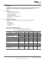
1
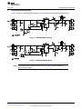
User's Guide
SLVU364 – March 2010
TPS62065/67EVM
This user’s guide describes the characteristics, operation, and use of the TPS62065-67EVM-347
evaluation module (EVM). The TPS62065-67EVM-347 is a fully assembled and tested platform for
evaluating the performance of both the TPS62065 and TPS62067 2-A step-down converters. This
document includes schematic diagrams, printed circuit board (PCB) layout, bill of materials, and test data.
Throughout this document, the abbreviations EVM, TPS62065/67EVM, and the term evaluation module
are synonymous with the TPS62065-67EVM-347 unless otherwise noted.
1
2
3
4
5
6
7
8
Contents
Introduction .................................................................................................................. 2
Electrical Performance Specifications .................................................................................... 2
TPS62056/67EVM Schematic ............................................................................................. 3
Connector and Test Point Descriptions .................................................................................. 4
Test Configuration .......................................................................................................... 6
TPS62065/67EVM Test Data .............................................................................................. 8
TPS62065/67EVM-347 Assembly Drawings and Layout ............................................................ 12
Bill of Materials ............................................................................................................. 18
List of Figures
................................................................................................
................................................................................................
Hardware Board Connection ..............................................................................................
TPS62065, TPS62067 Efficiency vs Load Current .....................................................................
TPS62065 Startup into 2.2-Ω Load .......................................................................................
TPS62067 Startup into 2.2-Ω Load .......................................................................................
TPS62067 Shutdown: No Load ...........................................................................................
TPS62065 Output Voltage Ripple (PFM Mode) .......................................................................
TPS62065 Output Voltage Ripple (PWM Mode) ......................................................................
TPS62065 Gain and Phase vs Frequency .............................................................................
TPS62065 Gain and Phase vs Frequency .............................................................................
TPS62065/67EVM Component Placement (Top View) ..............................................................
TPS62065/67EVM Top-Side Copper (Top View) .....................................................................
TPS62065/67EVM Internal Layer 2 (X-Ray View, from Top) ........................................................
TPS62065/67EVM Internal Layer 1 (X-Ray View, from Top) ........................................................
TPS62065/67EVM Bottom-Side Copper (Bottom View) .............................................................
1
TPS62065EVM Schematic
3
2
TPS62067EVM Schematic
3
3
4
5
6
7
8
9
10
11
12
13
14
15
16
6
8
8
9
9
10
10
11
11
13
14
15
16
17
List of Tables
1
TPS62065/67EVM Performance Characteristics ....................................................................... 2
2
TPS62065/67EVM Bill of Materials
.....................................................................................
18
All trademarks are the property of their respective owners.
SLVU364 – March 2010
Submit Documentation Feedback
TPS62065/67EVM
Copyright © 2010, Texas Instruments Incorporated
1
Introduction
1
www.ti.com
Introduction
The TPS62065-67EVM-347 is a fully assembled and tested pair of PCBs for evaluating the TPS62065
and TPS62067 2-A step-down converters. The EVM comes configured with both a TPS62065 IC and a
TPS62067 IC; there are two PCBs, one for each respective step-down converter IC.
1.1
Features
•
•
•
•
•
•
1.2
Input voltage range: 3.0 V to 6.0 V
Adjustable output voltage: 0.8 V to VIN
Up to 2.0-A output current
3-MHz switching frequency
Power Good output (TPS62067EVM only)
Clock dithering
TPS62065/67 Applications
The TPS62065 and TPS62067 step-down converters are ideal for these applications:
• POL
• Digital cameras
• PDAs, pocket PCs
• Portable media players
• DSP supply
2
Electrical Performance Specifications
Table 1 summarizes the TPS62065/67EVM performance specifications.
Table 1. TPS62065/67EVM Performance Characteristics
Parameter
Notes and
Conditions
Symbol
Min
Typ
Max
Units
Input Characteristics
Input Voltage
Input Undervoltage Lockout
(UVLO)
VIN
VIN_UVLO
6.0
V
Falling
1.73
3.0
1.78
1.83
V
Rising
1.9
1.95
1.98
V
Output Characteristics
Line Regulation
0
Load Regulation
–0.5
Output Current 1
Forward Current Limit
High-Side and Low Side
MOSFET
IOUT1 VIN = 3.0 V to 6.0 V
ILIMF VIN = 3.0 V to 6.0 V
%/V
%/A
2000
mA
2300
2750
3300
mA
2600
3000
3400
kHz
95
%
Systems Characteristics
Switching Frequency
fSW
Peak Efficiency
hpk VIN =Nom
Full Load Efficiency
2
VIN = 5.0 V, VIN =
h 1.8 V IOUT = 2,000
mA
TPS62065/67EVM
82
%
SLVU364 – March 2010
Submit Documentation Feedback
Copyright © 2010, Texas Instruments Incorporated
TPS62056/67EVM Schematic
www.ti.com
3
TPS62056/67EVM Schematic
Figure 1 shows the TPS62065EVM schematic. Figure 2 illustrates the TPS62067EVM schematic.
Figure 1. TPS62065EVM Schematic
Figure 2. TPS62067EVM Schematic
NOTE: These diagrams are provided for reference only. See Table 2, the Bill of Materials, for
specific component values.
SLVU364 – March 2010
Submit Documentation Feedback
TPS62065/67EVM
Copyright © 2010, Texas Instruments Incorporated
3
Connector and Test Point Descriptions
www.ti.com
4
Connector and Test Point Descriptions
4.1
Enable Jumpers/Switches: TPS62065EVM
4.1.1
J10 VIN
This header is the positive connection to the input power supply. The power supply must be connected
between J10 and J12 (GND). The leads to the input supply should be twisted and kept as short as
possible. The input voltage must be between 3.0 V and 6.0 V.
4.1.2
J11 S+/S–
J11 S+/S– are the sense connections for the input of the converter. Connect a voltmeter, or the sense
connection of a power supply or oscilloscope, to this header.
4.1.3
J12 GND
This header is the return connection to the input power supply. Connect the power supply between J12
and J10 (VIN). The leads to the input supply should be twisted and kept as short as possible. The input
voltage must be between 3.0 V and 6.0 V.
4.1.4
J13 VOUT
This header is the positive output of the step-down converter. The output voltage of the TPS62065 is
adjustable with feedback resistors R10 and R11. On the EVM, the output voltage is set to 1.8 V by default.
NOTE: A feed-forward capacitor is required. Refer to the TPS6206x data sheet (SLVS833) for
detailed information.
4.1.5
J14 S+/S–
J14 S+/S– are the sense connections for the output of the converter. Connect a voltmeter, or the sense
connection of an electronic load or oscilloscope, to this header.
4.1.6
J15 GND
J15 is the return connection of the converter. A load can be connected between J15 and J13 (VOUT). The
converter is capable of carrying a load current up to 2000 mA.
4.1.7
JP10 EN
This jumper enables/disables the TPS62065 on the EVM. Shorting jumper JP10 between the center pin
and On turns on the unit. Shorting the jumper between center pin and Off turns the unit off. A 1-MΩ
pull-up resistor is connected between VIN and EN. Removing jumper JP10 turns on the converter.
4.1.8
JP11 MODE
This jumper enables/disables the power-saving mode under light loads. Shorting jumper JP11 between
the center pin and PWM disables the power-saving mode; If the power save mode is disabled, the
converter operates in forced PWM mode over the entire load current range. Shorting the jumper between
the center pin and PWM/PSM enables the power-saving mode. The device operates in power-saving
mode under light load conditions. See the TPS6206x data sheet (SLVS833) for a detailed description of
this configuration. A 1-MΩ pulldown resistor is connected between GND and MODE. By removing JP11,
the converter operates in power-saving mode under light load conditions.
4
TPS62065/67EVM
SLVU364 – March 2010
Submit Documentation Feedback
Copyright © 2010, Texas Instruments Incorporated
Connector and Test Point Descriptions
www.ti.com
4.1.9
J16 VOUT (SMA)
This SMA connector is connected to the output voltage of the TPS62065. It can be used to easily analyze
the noise spectrum of the output voltage with a spectrum analyzer. By default, J16 is not assembled on
the EVM.
4.2
4.2.1
Enable Jumpers/Switches: TPS62067EVM
J20 VIN
This header is the positive connection to the input power supply. The power supply must be connected
between J10 and J12 (GND). The leads to the input supply should be twisted and kept as short as
possible. The input voltage must be between 3.0 V and 6.0 V.
4.2.2
J21 S+/S–
J21 S+/S– are the sense connections for the converter input. Connect a voltmeter, or the sense
connection of a power supply or an oscilloscope, to this header.
4.2.3
J22 GND
This header is the return connection to the input power supply. Connect the power supply between J22
and J20 (VIN). The leads to the input supply should be twisted and kept as short as possible. The input
voltage must be between 3.0 V and 6.0 V.
4.2.4
J23 VOUT
This header is the positive output of the step-down converter. The output voltage of the TPS62067 is
adjustable with the feedback resistors R20 and R21. On the EVM, the output voltage is set to 3.3 V by
default.
NOTE: There is a feed-forward capacitor required. Refer to the TPS6206x data sheet (SLVS833)
for detailed information.
4.2.5
J24 S+/S–
J24 S+/S– are the sense connections for the converter output. Connect a voltmeter, or the sense
connection of an electronic load or an oscilloscope, to this header.
4.2.6
J25 GND
J25 is the return connection of the converter. A load can be connected between J25and J23 (VOUT). The
converter is capable of a load up to 2,000 mA load current.
4.2.7
J26 PG
PG (Power Good) is an open-drain output. A 1-MΩ pull-up resistor is connected between VIN and PG.
This circuit is active once the device is enabled. It is driven by an internal comparatir that is connected to
the FB voltage. The PG output provides a high-level output once the FB voltage reaches 95% of its
nominal value. The PG output provides a low-level output when the FB voltage falls below 90% of its
nominal value.
NOTE: This function is only available on the TPS62067EVM.
SLVU364 – March 2010
Submit Documentation Feedback
TPS62065/67EVM
Copyright © 2010, Texas Instruments Incorporated
5
Test Configuration
4.2.8
www.ti.com
JP20 EN
This jumper enables/disables the TPS62067 device on the EVM. Shorting jumper JP20 between the
center pin and On turns on the unit. Shorting the jumper between center pin and Off turns the unit off. A
1-MΩ pull-up resistor is connected between VIN and EN. Removing jumper JP20 also turns on the
converter.
4.2.9
J27 VOUT (SMA)
This SMA connector is connected to the output voltage of the TPS62067. It can be used to easily analyze
the noise spectrum of the output voltage with a spectrum analyzer. By default, J27 is not assembled on
the EVM.
5
Test Configuration
5.1
Hardware Setup
Figure 3 illustrates a typical hardware test configuration.
Oscilloscope
JP10
-
VIN
VOUT
S+
S+
S-
S-
GND
GND
J13 J14 J15
+
DC
Power Supply
J12 J11 J10
ON EN OFF
Load
TPS62065/67EVM-347
Figure 3. Hardware Board Connection
6
TPS62065/67EVM
SLVU364 – March 2010
Submit Documentation Feedback
Copyright © 2010, Texas Instruments Incorporated
Test Configuration
www.ti.com
5.2
Testing Procedure
Follow these procedures when configuring the EVM for testing.
CAUTION
Many of the components on the TPS62065/67EVM-347 are susceptible to
damage by electrostatic discharge (ESD). Customers are advised to observe
proper ESD handling precautions when unpacking and handling the EVM,
including the use of a grounded wrist strap, bootstraps, or mats at an approved
ESD workstation. An electrostatic smock and safety glasses should also be
worn.
1. Connect a dc power supply between J10 and J12 on the TPS62065EVM, or J20 and J22 on the
TPS62067EVM. Please note that the input voltage should be between 3.0 V and 6.0 V. Keep the wires
from the input power supply to the EVM as short as possible and twisted.
2. Connect a dc voltmeter or oscilloscope to the output sense connection of the EVM (J14 on the
TPS62065EVM, J24 on the TPS62067EVM).
3. A load can be connected between J13 and J15 on the TPS62065EVM, or J23 and J25 on the
TPS62067EVM.
4. To enable the converter, connect the shorting bar on JP10 (JP20) between EN and ON on the
TPS62065EVM (TPS62067EVM).
5. The TPS62065EVM has a feature to allow the user to switch between Power-Save Mode under light
loads and forced PWM mode; this feature is enabled or disabled with jumper JP11. This feature is only
available on the TPS62065EVM.
6. The TPS62067EVM has a PG (Power Good) output. The PG pin on the TPS62067 is connected to
J26. PG is an open-drain output. The output is pulled up with a 1-MΩ pull-up resistor (R22) to VIN.
This feature is only available on the TPS62067EVM.
SLVU364 – March 2010
Submit Documentation Feedback
TPS62065/67EVM
Copyright © 2010, Texas Instruments Incorporated
7
TPS62065/67EVM Test Data
6
www.ti.com
TPS62065/67EVM Test Data
Figure 4 through Figure 11 present typical performance curves for the TPS62065/67EVM. Actual
performance data can be affected by measurement techniques and environmental variables; therefore,
these curves are presented for reference and may differ from actual results obtained by some users.
6.1
Efficiency
Figure 4 shows the typical efficiency performance for the TPS62065 and TPS62067.
EFFICIENCY vs LOAD CURRENT
100
95
Efficiency (%)
90
85
80
75
70
VIN = 3.0 V
VIN = 3.3 V
VIN = 3.6 V
VIN = 4.2 V
VIN = 5.0V
65
60
55
L = 1.0 mH (LQH441R0)
COUT = 10 mF (0603 size)
VOUT =1.8 V
Mode: Auto PFM/PWM
50
0
0.2
0.4
0.6
0.8
1.0
1.2
1.4
1.6
1.8
2.0
IOUT (A)
Figure 4. TPS62065, TPS62067 Efficiency vs Load Current
6.2
Start-up: TPS62065
Figure 5 shows the typical start-up performance for the TPS62065 using the TPS62065EVM.
TPS62065 Startup
2 V/div
1 V/div
2 A/div
500 mA/div
L = 1.2 mH
COUT = 10 mF
500 mA/div
VIN = 3.6 V
VOUT = 1.8 V
Load = R2R
Time (100 ms/div)
Conditions: VIN = 3.6 V, VOUT = 1.8 V
Figure 5. TPS62065 Startup into 2.2-Ω Load
8
TPS62065/67EVM
SLVU364 – March 2010
Submit Documentation Feedback
Copyright © 2010, Texas Instruments Incorporated
TPS62065/67EVM Test Data
www.ti.com
6.3
Start-up and Shutdown: TPS62067
Figure 6 and Figure 7 illustrate the typical start-up and shutdown behavior, respectively, for the
TPS62067, using the TPS62067EVM.
TPS62067 Startup
2 V/div
2 V/div
1 A/div
VIN = 4.2 V
VOUT = 3.3 V
Load = 2R2
PG Pull-up Resistor = 10 kW
2 V/div
Time (100 ms/div)
Conditions: VIN = 4.2 V, VOUT = 3.3 V
Figure 6. TPS62067 Startup into 2.2-Ω Load
TPS62067 Shutdown
2 V/div
VIN = 4.2 V
VOUT = 3.3 V
Load = No Load
PG Pull-up Resistor = 10 kW
2 V/div
5 V/div
Time (1 ms/div)
Conditions: VIN = 4.2 V, VOUT = 3.3 V
Figure 7. TPS62067 Shutdown: No Load
SLVU364 – March 2010
Submit Documentation Feedback
TPS62065/67EVM
Copyright © 2010, Texas Instruments Incorporated
9
TPS62065/67EVM Test Data
6.4
www.ti.com
Output Voltage Ripple (Power-Save Mode)
Figure 8 and Figure 9 show the typical output voltage ripple for the TPS62065 in PFM and PWM modes,
respectively, with the TPS62065EVM.
TYPICAL OUTPUT VOLTAGE RIPPLE (PFM MODE)
VOUT:
50 mV/div
VIN = 3.6 V
VOUT = 1.8 V
IOUT = 20 mA L = 1.2 mH
MODE = GND COUT = 10 mF
SW:
2 V/div
ICOIL:
200 mA/div
Time (4 ms/div)
Figure 8. TPS62065 Output Voltage Ripple (PFM Mode)
TYPICAL OUTPUT VOLTAGE RIPPLE (PWM MODE)
VOUT:
50 mV/div
SW:
2 V/div
ICOIL:
500 mA/div
IOUT = 500 mA L = 1.2 mH
VIN = 3.6 V
VOUT = 1.8 V MODE = GND COUT = 10 mF
Time (100 ns/div)
Figure 9. TPS62065 Output Voltage Ripple (PWM Mode)
10
TPS62065/67EVM
SLVU364 – March 2010
Submit Documentation Feedback
Copyright © 2010, Texas Instruments Incorporated
TPS62065/67EVM Test Data
www.ti.com
6.5
Control Loop Bode Diagrams: TPS62065
Figure 10 and Figure 11 illustrate typical TPS62065 gain and phase performance versus frequency at VIN
= 3.6 V and 5.0 V, respectively, using the TPS62025EVM.
Conditions: VIN = 3.6 V, VOUT = 1.8 V, IOUT = 1.6 A; bandwidth: 224 kHz, phase margin: 59°
Figure 10. TPS62065 Gain and Phase vs Frequency
Conditions: VIN = 5.0 V, VOUT = 1.8 V, IOUT = 1.6 A; bandwidth: 271 kHz, phase margin: 54°
Figure 11. TPS62065 Gain and Phase vs Frequency
SLVU364 – March 2010
Submit Documentation Feedback
TPS62065/67EVM
Copyright © 2010, Texas Instruments Incorporated
11
TPS62065/67EVM-347 Assembly Drawings and Layout
7
www.ti.com
TPS62065/67EVM-347 Assembly Drawings and Layout
Figure 12 through Figure 16 show the design of the TPS62065/67EVM-347 printed circuit boards. This
EVM has been designed using a four-layer, 1-ounce copper-clad PCB (3.81 cm by 4.57 cm) with all
components in an active area on the top side of the board. All active traces to the top and bottom layers to
allow the user to easily view, probe, and evaluate the TPS62025/67 control ICs in a practical,
double-sided application environment. Moving components to both sides of the PCB or using additional
internal layers can offer additional size reduction for space-constrained systems.
NOTE: Board layouts are not to scale. These figures are intended to show how the board is laid
out; they are not intended to be used for manufacturing TPS62065/67EVM-347 PCBs.
12
TPS62065/67EVM
SLVU364 – March 2010
Submit Documentation Feedback
Copyright © 2010, Texas Instruments Incorporated
TPS62065/67EVM-347 Assembly Drawings and Layout
www.ti.com
38.10 mm
(1.50 inch)
38.10 mm
(1.50 inch)
45.72 mm
(1.80 inch)
Figure 12. TPS62065/67EVM Component Placement (Top View)
SLVU364 – March 2010
Submit Documentation Feedback
TPS62065/67EVM
Copyright © 2010, Texas Instruments Incorporated
13
TPS62065/67EVM-347 Assembly Drawings and Layout
www.ti.com
Figure 13. TPS62065/67EVM Top-Side Copper (Top View)
14
TPS62065/67EVM
SLVU364 – March 2010
Submit Documentation Feedback
Copyright © 2010, Texas Instruments Incorporated
TPS62065/67EVM-347 Assembly Drawings and Layout
www.ti.com
Figure 14. TPS62065/67EVM Internal Layer 2 (X-Ray View, from Top)
SLVU364 – March 2010
Submit Documentation Feedback
TPS62065/67EVM
Copyright © 2010, Texas Instruments Incorporated
15
TPS62065/67EVM-347 Assembly Drawings and Layout
www.ti.com
Figure 15. TPS62065/67EVM Internal Layer 1 (X-Ray View, from Top)
16
TPS62065/67EVM
SLVU364 – March 2010
Submit Documentation Feedback
Copyright © 2010, Texas Instruments Incorporated
TPS62065/67EVM-347 Assembly Drawings and Layout
www.ti.com
Figure 16. TPS62065/67EVM Bottom-Side Copper (Bottom View)
SLVU364 – March 2010
Submit Documentation Feedback
TPS62065/67EVM
Copyright © 2010, Texas Instruments Incorporated
17
Bill of Materials
8
www.ti.com
Bill of Materials
Table 2 lists the bill of materials for the TPS62065/67EVM.
Table 2. TPS62065/67EVM Bill of Materials (1) (2) (3) (4)
(1)
(2)
(3)
(4)
18
Count
RefDes
Value
2
C10, C20
22 mF
Capacitor, ceramic, 10 V, X7R, 10%
Description
1210
Size
GRM32ER71A226K
Part Number
MuRata
2
C11, C21
22 pF
Capacitor, ceramic, 10 V, NGO, 5%
0603
Standard
Standard
4
C12, C13,
C22, C23
10 mF
Capacitor, ceramic, 6.3 V, X5R, 20%
0603
GRM188R60J106ME47
D
muRata
0
C14, C24
Open
Capacitor, ceramic, 6.3 V, X5R, 20%
0603
GRM188R60J106ME47
D
muRata
0.210 in2
901-144-8RFX
MFR
0
J16, J27
Open
Connector, SMA , straight, PC mount
2
L10, L20
1.0 mH
Inductor, chip coil, ±30%
1515
LQH44PN1R0NP0L
AMP
1
R10
360 kΩ
Resistor, chip, 1/16W, 1%
0603
Standard
Std
2
R11, R21
180 kΩ
Resistor, chip, 1/16W, 1%
0603
Standard
Std
1
R20
820 kΩ
Resistor, chip, 1/16W, 1%
0603
Standard
Std
4
R12, R13,
R22, R23
1.00 MΩ
Resistor, chip, 1/16W, 1%
0603
Standard
Std
1
U10
TPS62065DSG
IC, step-down converter, 3 MHz, 1.6 A
SON-8
TPS62065DSG
TI
1
U20
TPS62067DSG
IC, step-down converter, 3 MHz, 1.6 A
SON-8
TPS62067DSG
TI
Murata
These assemblies are ESD sensitive. ESD precautions must be observed.
These assemblies must be clean and free from flux and all contaminants. Use of no-clean flux is not acceptable.
These assemblies must comply with workmanship standards IPC-A-610 Class 2.
Reference designators marked with an asterisk (**) cannot be substituted. All other components can be substituted with equivalent
manufacturing components.
TPS62065/67EVM
SLVU364 – March 2010
Submit Documentation Feedback
Copyright © 2010, Texas Instruments Incorporated
Evaluation Board/Kit Important Notice
Texas Instruments (TI) provides the enclosed product(s) under the following conditions:
This evaluation board/kit is intended for use for ENGINEERING DEVELOPMENT, DEMONSTRATION, OR EVALUATION
PURPOSES ONLY and is not considered by TI to be a finished end-product fit for general consumer use. Persons handling the
product(s) must have electronics training and observe good engineering practice standards. As such, the goods being provided are
not intended to be complete in terms of required design-, marketing-, and/or manufacturing-related protective considerations,
including product safety and environmental measures typically found in end products that incorporate such semiconductor
components or circuit boards. This evaluation board/kit does not fall within the scope of the European Union directives regarding
electromagnetic compatibility, restricted substances (RoHS), recycling (WEEE), FCC, CE or UL, and therefore may not meet the
technical requirements of these directives or other related directives.
Should this evaluation board/kit not meet the specifications indicated in the User’s Guide, the board/kit may be returned within 30
days from the date of delivery for a full refund. THE FOREGOING WARRANTY IS THE EXCLUSIVE WARRANTY MADE BY
SELLER TO BUYER AND IS IN LIEU OF ALL OTHER WARRANTIES, EXPRESSED, IMPLIED, OR STATUTORY, INCLUDING
ANY WARRANTY OF MERCHANTABILITY OR FITNESS FOR ANY PARTICULAR PURPOSE.
The user assumes all responsibility and liability for proper and safe handling of the goods. Further, the user indemnifies TI from all
claims arising from the handling or use of the goods. Due to the open construction of the product, it is the user’s responsibility to
take any and all appropriate precautions with regard to electrostatic discharge.
EXCEPT TO THE EXTENT OF THE INDEMNITY SET FORTH ABOVE, NEITHER PARTY SHALL BE LIABLE TO THE OTHER
FOR ANY INDIRECT, SPECIAL, INCIDENTAL, OR CONSEQUENTIAL DAMAGES.
TI currently deals with a variety of customers for products, and therefore our arrangement with the user is not exclusive.
TI assumes no liability for applications assistance, customer product design, software performance, or infringement of
patents or services described herein.
Please read the User’s Guide and, specifically, the Warnings and Restrictions notice in the User’s Guide prior to handling the
product. This notice contains important safety information about temperatures and voltages. For additional information on TI’s
environmental and/or safety programs, please contact the TI application engineer or visit www.ti.com/esh.
No license is granted under any patent right or other intellectual property right of TI covering or relating to any machine, process, or
combination in which such TI products or services might be or are used.
FCC Warning
This evaluation board/kit is intended for use for ENGINEERING DEVELOPMENT, DEMONSTRATION, OR EVALUATION
PURPOSES ONLY and is not considered by TI to be a finished end-product fit for general consumer use. It generates, uses, and
can radiate radio frequency energy and has not been tested for compliance with the limits of computing devices pursuant to part 15
of FCC rules, which are designed to provide reasonable protection against radio frequency interference. Operation of this
equipment in other environments may cause interference with radio communications, in which case the user at his own expense
will be required to take whatever measures may be required to correct this interference.
EVM Warnings and Restrictions
It is important to operate this EVM within the input voltage range of 3.0 V to 6.0 V and the output voltage range of 0.8 V to 6.0 V.
Exceeding the specified input range may cause unexpected operation and/or irreversible damage to the EVM. If there are
questions concerning the input range, please contact a TI field representative prior to connecting the input power.
Applying loads outside of the specified output range may result in unintended operation and/or possible permanent damage to the
EVM. Please consult the EVM User's Guide prior to connecting any load to the EVM output. If there is uncertainty as to the load
specification, please contact a TI field representative.
During normal operation, some circuit components may have case temperatures greater than +60°C. The EVM is designed to
operate properly with certain components above +60°C as long as the input and output ranges are maintained. These components
include but are not limited to linear regulators, switching transistors, pass transistors, and current sense resistors. These types of
devices can be identified using the EVM schematic located in the EVM User's Guide. When placing measurement probes near
these devices during operation, please be aware that these devices may be very warm to the touch.
Mailing Address: Texas Instruments, Post Office Box 655303, Dallas, Texas 75265
Copyright © 2010, Texas Instruments Incorporated
IMPORTANT NOTICE
Texas Instruments Incorporated and its subsidiaries (TI) reserve the right to make corrections, modifications, enhancements, improvements,
and other changes to its products and services at any time and to discontinue any product or service without notice. Customers should
obtain the latest relevant information before placing orders and should verify that such information is current and complete. All products are
sold subject to TI’s terms and conditions of sale supplied at the time of order acknowledgment.
TI warrants performance of its hardware products to the specifications applicable at the time of sale in accordance with TI’s standard
warranty. Testing and other quality control techniques are used to the extent TI deems necessary to support this warranty. Except where
mandated by government requirements, testing of all parameters of each product is not necessarily performed.
TI assumes no liability for applications assistance or customer product design. Customers are responsible for their products and
applications using TI components. To minimize the risks associated with customer products and applications, customers should provide
adequate design and operating safeguards.
TI does not warrant or represent that any license, either express or implied, is granted under any TI patent right, copyright, mask work right,
or other TI intellectual property right relating to any combination, machine, or process in which TI products or services are used. Information
published by TI regarding third-party products or services does not constitute a license from TI to use such products or services or a
warranty or endorsement thereof. Use of such information may require a license from a third party under the patents or other intellectual
property of the third party, or a license from TI under the patents or other intellectual property of TI.
Reproduction of TI information in TI data books or data sheets is permissible only if reproduction is without alteration and is accompanied
by all associated warranties, conditions, limitations, and notices. Reproduction of this information with alteration is an unfair and deceptive
business practice. TI is not responsible or liable for such altered documentation. Information of third parties may be subject to additional
restrictions.
Resale of TI products or services with statements different from or beyond the parameters stated by TI for that product or service voids all
express and any implied warranties for the associated TI product or service and is an unfair and deceptive business practice. TI is not
responsible or liable for any such statements.
TI products are not authorized for use in safety-critical applications (such as life support) where a failure of the TI product would reasonably
be expected to cause severe personal injury or death, unless officers of the parties have executed an agreement specifically governing
such use. Buyers represent that they have all necessary expertise in the safety and regulatory ramifications of their applications, and
acknowledge and agree that they are solely responsible for all legal, regulatory and safety-related requirements concerning their products
and any use of TI products in such safety-critical applications, notwithstanding any applications-related information or support that may be
provided by TI. Further, Buyers must fully indemnify TI and its representatives against any damages arising out of the use of TI products in
such safety-critical applications.
TI products are neither designed nor intended for use in military/aerospace applications or environments unless the TI products are
specifically designated by TI as military-grade or "enhanced plastic." Only products designated by TI as military-grade meet military
specifications. Buyers acknowledge and agree that any such use of TI products which TI has not designated as military-grade is solely at
the Buyer's risk, and that they are solely responsible for compliance with all legal and regulatory requirements in connection with such use.
TI products are neither designed nor intended for use in automotive applications or environments unless the specific TI products are
designated by TI as compliant with ISO/TS 16949 requirements. Buyers acknowledge and agree that, if they use any non-designated
products in automotive applications, TI will not be responsible for any failure to meet such requirements.
Following are URLs where you can obtain information on other Texas Instruments products and application solutions:
Products
Applications
Amplifiers
amplifier.ti.com
Audio
www.ti.com/audio
Data Converters
dataconverter.ti.com
Automotive
www.ti.com/automotive
DLP® Products
www.dlp.com
Communications and
Telecom
www.ti.com/communications
DSP
dsp.ti.com
Computers and
Peripherals
www.ti.com/computers
Clocks and Timers
www.ti.com/clocks
Consumer Electronics
www.ti.com/consumer-apps
Interface
interface.ti.com
Energy
www.ti.com/energy
Logic
logic.ti.com
Industrial
www.ti.com/industrial
Power Mgmt
power.ti.com
Medical
www.ti.com/medical
Microcontrollers
microcontroller.ti.com
Security
www.ti.com/security
RFID
www.ti-rfid.com
Space, Avionics &
Defense
www.ti.com/space-avionics-defense
RF/IF and ZigBee® Solutions www.ti.com/lprf
Video and Imaging
www.ti.com/video
Wireless
www.ti.com/wireless-apps
Mailing Address: Texas Instruments, Post Office Box 655303, Dallas, Texas 75265
Copyright © 2010, Texas Instruments Incorporated