1
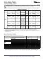
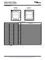
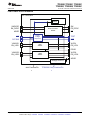
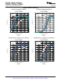
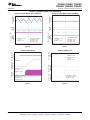
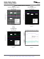
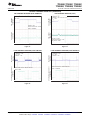
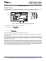
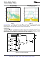
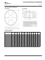
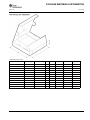
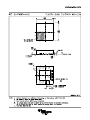
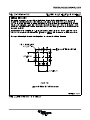
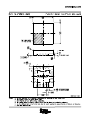
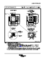
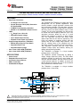
TPS65000, TPS65001, TPS650001
TPS650003, TPS650006, TPS650061
www.ti.com
SLVS810B – JUNE 2009 – REVISED AUGUST 2010
2.25 MHz Step Down Converter with Dual LDOs and SVS
Check for Samples: TPS65000, TPS65001, TPS650001, TPS650003, TPS650006, TPS650061
FEATURES
1
•
2
•
•
•
•
DESCRIPTION
Step-Down Converters:
– VIN Range From 2.3V to 6V
– Spread Spectrum Clock (SSC) Generation
for Reduced EMI
– 2.25MHz Fixed Frequency Operation
– 600mA or 1A (TPS650061) Output Current
LDOs:
– VIN Range From 1.6V to 6V
– Adjustable Output Voltage
– Up to 300mA Output Current
– Separate Power Inputs and Enables
Supply Voltage Supervisor (TPS65001)
– Manual Reset Input for Push Button
– Adjustable Reset Time
– Adjustable Reset Voltage
3mm × 3mm 16-Pin QFN (TPS65000)
3mm × 3mm 20-Pin QFN (TPS65001)
The TPS65000 and TPS65001 are single chip Power
Management ICs for portable applications. Both
devices combine a single step-down converter with
two low dropout regulators. The step-down converter
enters a low power mode at light load for maximum
efficiency across the widest possible range of load
currents. For low noise applications, the devices can
be forced into fixed frequency PWM via a pin. The
step-down converter allows the use of a small
inductor and capacitors to achieve a small solution
size. The step-down converter has Power Good
status output that can be used for sequencing. The
LDOs are capable of supplying 300mA, and can
operate with an input voltage range between 1.6V
and 6V, allowing them to be supplied from the
step-down converter or directly from the main battery.
The step-down converter and the LDOs have
separate voltage inputs and enables, allowing for
design and sequencing flexibility.
The TPS65000 is available in a 16-pin leadless
package (3mm × 3mm QFN).
APPLICATIONS
•
•
•
•
•
The TPS65001 extends functionality by adding a
Supply Voltage Supervisor (SVS). The SVS allows
maximum flexibility by having the reset voltage set
with two external resistors, and the reset time set by
a small external capacitor. In addition, an active low
Manual Reset input allows the SVS to be connected
to a push button for external control.
Point of Load
Embedded Processor Power
Cell Phones, Smart-Phones
PDAs, Pocket PCs
Portable Media Players
The TPS65001 is available in a 20-pin leadless
package (3mm × 3mm QFN).
TPS65000/1
Oscillator
SSCG
EN_DCDC
VINDCDC
VIN
10mF
A
P
475kW
VIN
0.1mF
470kW
A
MR
A
VIN
Supply
Voltage
Supervisor
TRST
A
VLDO1
470kW
LDO1
300mA
180kW
A
VLDO2
EN_LDO2
VDCDC
A
VIN
470kW
PGND
AGND
10mF
180kW
P
VLDO1
1.8V
P
820kW
FB_LDO2
LDO2
300mA
100kW
PG
RST
FB_LDO1
VINLDO2
22pF
RST
EN_LDO1
VINLDO1
VDCDC
3.3V
10mF
P
150kW
A
PG
100nF
A
680W
FB_DCDC
MODE
RSTSNS
232kW
2.2mH
SW
Step-Down
600mA
10mF
VLDO2
2.8V
P
A
Bandgap Reference
TPS65000/01 Joint Function/Pin
TPS65001 Only Function/Pin
1
2
Please be aware that an important notice concerning availability, standard warranty, and use in critical applications of Texas
Instruments semiconductor products and disclaimers thereto appears at the end of this data sheet.
PowerPAD is a trademark of Texas Instruments.
PRODUCTION DATA information is current as of publication date.
Products conform to specifications per the terms of the Texas
Instruments standard warranty. Production processing does not
necessarily include testing of all parameters.
Copyright © 2009–2010, Texas Instruments Incorporated
TPS65000, TPS65001, TPS650001
TPS650003, TPS650006, TPS650061
SLVS810B – JUNE 2009 – REVISED AUGUST 2010
www.ti.com
This integrated circuit can be damaged by ESD. Texas Instruments recommends that all integrated circuits be handled with
appropriate precautions. Failure to observe proper handling and installation procedures can cause damage.
ESD damage can range from subtle performance degradation to complete device failure. Precision integrated circuits may be more
susceptible to damage because very small parametric changes could cause the device not to meet its published specifications.
ORDERING INFORMATION
TA
PART
NUMBER (1)
PACKAGE
PACKAGE
DESIGNATOR
TPS65000
QFN 3×3 16
RTE
TPS65001
QFN 3×3 20
RUK
TPS650001
–40°C to
85°C
TPS650003
TPS650006
TPS650061
(1)
(2)
QFN 3×3 16
QFN 3×3 16
QFN 3×3 16
QFN 3×3 20
OPTIONS
SVS
SSC
ORDERING (2)
PACKAGE
MARKING
LDO voltages
externally adjustable
DCDC converters
600mA, VOUT
externally adjustable
N/A
Included
TPS65000RTE
CFO
Included
Included
TPS65001RUK
CFQ
RTE
LDO1 = 1.8V fixed,
LDO2 = 2.8V fixed,
DCDC Converter
600MA, DCDC
VOUT = 1.2V fixed
N/A
Included
TPS650001RTE
DAG
RTE
LDO1 = 3.3V fixed,
LDO2 = 1.8V fixed,
DCDC Converter
600MA, DCDC
VOUT = 1.5V fixed
N/A
Included
TPS650003RTE
DAH
RTE
LDO1 = 1.8V fixed,
LDO2 = 3.3V fixed,
DCDC Converter
600MA, DCDC
VOUT = 1.2V fixed
N/A
Included
TPS650006RTE
DAI
RUK
LDO1 = 3.3V fixed,
LDO2 = 1.8V fixed,
DCDC Converter 1A,
VOUT externally
adjustable
Included
Included
TPS650061RUK
DAJ
TPS650001, TPS650003, and TPS650006 are spin versions of TPS65000. TPS650061 is a spin version of TPS65001. Different DCDC
current limits and fixed voltage outputs of the DCDC and LDOs are available. Please contact your Texas Instruments sales
representative for further information.
For the most current package and ordering information, see the Package Option Addendum at the end of this document, or see the TI
website at www.ti.com.
ABSOLUTE MAXIMUM RATINGS
over operating free-air temperature range (unless otherwise noted) (1)
Input voltage range
Output voltage range
Current
MIN
MAX
On all pins except AGND, PGND, EN_DCDC, VLDO1,
VLDO2, FB_LDO1, FB_LDO2, FB_DCDC pins with
respect to AGND
–0.3
7
On EN_DCDC with respect to AGND
-0.3
VIN + 0.3, ≤ 7
On VLDO1, VLDO2, FB_LDO1, FB_LDO2, FB_DCDC
-0.3
3.6
V
1800
mA
VINLDO1/2, VLDO1/2, AGND
800
mA
1
mA
at all other pins
Operating free-air temperature, TA
See dissipation rating table
-40
Maximum junction temperature, TJ
Storage temperature, Tstg
2
V
VINDCDC, SW, PGND,
Continuous total power dissipation
(1)
UNIT
-65
85
°C
125
°C
150
°C
Stresses beyond those listed under absolute maximum ratings may cause permanent damage to the device. These are stress ratings
only and functional operation of the device at these or any other conditions beyond those indicated under recommended operating
conditions is not implied. Exposure to absolute-maximum-rated conditions for extended periods may affect device reliability.
Submit Documentation Feedback
Copyright © 2009–2010, Texas Instruments Incorporated
Product Folder Link(s): TPS65000 TPS65001 TPS650001 TPS650003 TPS650006 TPS650061
TPS65000, TPS65001, TPS650001
TPS650003, TPS650006, TPS650061
www.ti.com
SLVS810B – JUNE 2009 – REVISED AUGUST 2010
DISSIPATION RATINGS
DEVICE
PACKAGE
TPS65000/01 (1)
RTE / RUK
TPS65000/01 (2)
(1)
(2)
TA ≤ 25°C
TA = 70°C
TA = 85°C
POWER RATING POWER RATING POWER RATING
RqJA
RqJB
270°C/W
14°C/W
370 mW
204 mW
148 mW
48.7°C/W
14°C/W
2.05 W
1.13 W
821 mW
The JEDEC low-K (1s) board used to derive this data was a 3in × 3in, two-layer board with 2-ounce copper traces on top of the board.
The JEDEC high-K (2s2p) board used to derive this data was a 3in × 3in, multilayer board with 1-ounce internal power and ground.
RECOMMENDED OPERATING CONDITIONS
L1
CI
CO
MIN
NOM
MAX
SW pin inductor
1.5
2.2
3.3
Input capacitor at VINDCDC
10
Input capacitor at VINLDO1/2
2.2
Output capacitor for DCDC
10
Output capacitor for LDO1/2
2.2
mF
22
LDO1 output current
LDO2 output current
Operating ambient temperature
mF
mF
DCDC converter output current (TPS650061 ONLY)
TA
mH
mF
DCDC converter output current
IO
UNIT
-40
600
mA
1000
mA
300
mA
300
mA
85
°C
ELECTRICAL CHARACTERISTICS
Over full operating ambient temperature range, typical values are at TA = 25° C. Unless otherwise noted, specifications apply
for condition VIN = EN_LDOx = EN_DCDC = 3.6 V. External components L = 2.2 mH, COUT = 10 mF, CIN = 4.7 mF, (see the
parameter measurement information).
PARAMETER
TEST CONDITIONS
MIN
TYP
MAX
UNIT
OPERATING VOLTAGE
Input voltage for VINDCDC of
DCDC converter
VIN
6
See
(1)
1.6
6
Input voltage for LDO2 (VINLDO2)
See
(1)
1.6
6
Internal undervoltage lockout
threshold
VCC falling
Input voltage for LDO1 (VINLDO1)
UVLO
2.3
Internal undervoltage lockout
hysteresis
1.72
1.77
1.82
160
V
V
mV
SUPPLY CURRENT TPS65000
IQ
Operating quiescent current
MODE low, EN_DCDC high,
EN_LDO1/2 low,
IOUT = 0 mA and no switching
23
MODE low, EN_DCDC low,
EN_LDO1/2 high, IOUT = 0mA
IOUT = 0 mA and no switching (2)
50
mA
EN_DCDC high, MODE high,
EN_LDO1/2 low, IOUT = 0mA
ISD
(1)
(2)
Shutdown Current
EN_DCDC low EN_LDO1 and EN_LDO2 low
32
57
4
0.16
mA
2.2
mA
The design principle allows only VINDCDC to be the highest supply in the system if different voltage input supplies separately to DCDC
converter and LDOs, meaning VINDCDC ≥ VINLDO1, VINDCDC ≥ VINLDO2.
The max quiescent current of enabling LDOs is 8mA higher for TPS650001, TPS650003, TPS650006 and TPS650061.
Copyright © 2009–2010, Texas Instruments Incorporated
Submit Documentation Feedback
Product Folder Link(s): TPS65000 TPS65001 TPS650001 TPS650003 TPS650006 TPS650061
3
TPS65000, TPS65001, TPS650001
TPS650003, TPS650006, TPS650061
SLVS810B – JUNE 2009 – REVISED AUGUST 2010
www.ti.com
ELECTRICAL CHARACTERISTICS (continued)
Over full operating ambient temperature range, typical values are at TA = 25° C. Unless otherwise noted, specifications apply
for condition VIN = EN_LDOx = EN_DCDC = 3.6 V. External components L = 2.2 mH, COUT = 10 mF, CIN = 4.7 mF, (see the
parameter measurement information).
PARAMETER
TEST CONDITIONS
MIN
TYP
MAX
UNIT
MODE low, EN_DCDC high,
EN_LDO1/2 low,
IOUT = 0 mA and no switching
24
37
mA
MODE low, EN_DCDC low,
EN_LDO1/2 high, IOUT = 0mA
IOUT = 0 mA and no switching (3)
55
62
mA
SUPPLY CURRENT TPS65001
IQ
Operating quiescent current
EN_DCDC high, MODE high,
EN_LDO1/2 low, IOUT = 0mA
ISD
Shutdown Current
4
EN_DCDC low EN_LDO1 and EN_LDO2 low
11
mA
17
mA
DIGITAL PINS (EN_DCDC, EN_LDO1, EN_LDO2, MODE, PG, MR, RST
VIH
High level input voltage
VIL
Low level input voltage
1.2
VOL
Low level output voltage
PG and RST pins only, IO = -100mA
Ilkg
Input leakage current
MODE, EN_DCDC, EN_LDO1, EN_LDO2 tied to
GND or VINDCDC
V
0.4
V
0.4
V
0.01
0.1
mA
2.25
2.847
240
480
185
380
OSCILLATOR
fSW
Oscillator frequency
1.722
MHz
STEP DOWN CONVERTER POWER SWITCH
High side MOSFET on-resistance
RDS(on)
Low side MOSFET on-resistance
VINDCDC = VGS = 3.6V
2.3 V ≤ VINDCDC ≤ 2.5V
300
2.5 V ≤ VINDCDC ≤ 6V
600
mΩ
IO
DC output current
IO
DC output current (TPS650061
ONLY)
2.7 V ≤ VINDCDC ≤ 6V
ILIMF
Forward current limit PMOS and
NMOS
2.3 V ≤ VINDCDC ≤ 6V
800
1000
1400
mA
ILIMF
Forward current limit PMOS and
NMOS (TPS650061 ONLY)
2.7 V ≤ VINDCDC ≤ 6V
1200
1500
1680
mA
Thermal shutdown
Increasing junction temperature
150
Thermal shutdown hysteresis
Decreasing junction temperature
30
TSD
1000
mA
mA
°C
STEP DOWN CONVERTER OUTPUT VOLTAGE
VDCDC
Adjustable output voltage range,
DCDC
0.6
VINDCDC
V
0.1
mA
V
FB_DCDC pin current
Vref
Internal reference voltage
VDCDC
Output Voltage Accuracy (PWM
Mode) (4)
MODE = high,
2.3 ≤ VINDCDC ≤ 6V
Output Voltage Accuracy (PFM
mode) (5)
MODE low
+1% voltage positioning active
0.594
0.6
0.606
–1.5%
0%
1.5%
1%
Load regulation (PWM mode)
MODE high
0.5
%/A
tStart
Start-up time
EN_DCDC to start of switching (10%)
250
ms
tRamp
VDCDC ramp up time
VDCDC ramp from 10% to 90%
250
ms
RDIS
Internal discharge resistance at
SW
EN_DCDC low
450
Ω
(3)
(4)
(5)
4
The max quiescent current of enabling LDOs is 8mA higher for TPS650001, TPS650003, TPS650006 and TPS650061.
For VINDCDC = VDCDC + 1V
In PFM Mode, the internal reference voltage is typ 1.01 × VREF.
Submit Documentation Feedback
Copyright © 2009–2010, Texas Instruments Incorporated
Product Folder Link(s): TPS65000 TPS65001 TPS650001 TPS650003 TPS650006 TPS650061
TPS65000, TPS65001, TPS650001
TPS650003, TPS650006, TPS650061
www.ti.com
SLVS810B – JUNE 2009 – REVISED AUGUST 2010
ELECTRICAL CHARACTERISTICS (continued)
Over full operating ambient temperature range, typical values are at TA = 25° C. Unless otherwise noted, specifications apply
for condition VIN = EN_LDOx = EN_DCDC = 3.6 V. External components L = 2.2 mH, COUT = 10 mF, CIN = 4.7 mF, (see the
parameter measurement information).
PARAMETER
TEST CONDITIONS
MIN
TYP
MAX
UNIT
LOW DROP OUT REGULATORS
VI
Input voltage for LDOx (VINLDOx)
VO
Adjustable output voltage, LDOx
(VLDOx) (6)
IO
Continuous Pass FET Current
ISC
Short circuit current limit
1.6
6
V
0.73
VINLDOx - VDO
V
300
2.3V ≤ VINLDOx
340
700
VINLDOx < 2.3V
210
700
FB_LDOx pin current
FB_LDOx voltage
VDO
Dropout Voltage
mA
VINLDOx ≥ 2.3V, IOUT = 250mA
370
mV
VINLDOx < 2.3V IOUT = 175mA
370
mV
0.5
V
IO = 1mA to 300mA, VINLDOx = 2.3 - 6V,
VLDOx = 1.2V
-3.5%
3.5%
IO = 1mA to 175mA VINLDOx = 1.6V - 6V,
VLDOx = 1.2V
-3.5%
3.5%
Load regulation
IO = 1mA to 300mA VINLDOx = 3.6V
VLDOx = 1.2V
-1.5%
1.5%
Line regulation
VINLDOx = 1.6V - 6V VLDOx = 1.2V at
IO = 1mA
-0.5%
0.5%
PSRR
Power Supply Rejection Ratio
fNOISE ≤ 10kHz, COUT ≥ 2.2mF, VIN = 2.3V,
VOUT = 1.3V IOUT = 10mA
tRAMP
VLDOx Ramp Time
RDIS
Internal discharge resistance at
VLDOx
TSD
Output Voltage Accuracy
(8)
mA
0.1
Adjustable VOUT mode only
(7)
mA
40
dB
VLDOx ramp from 10% to 90%
200
ms
EN_LDOx low
450
Ω
Thermal shutdown
Increasing temperature
150
°C
Thermal shutdown hysteresis
Decreasing temperature
30
°C
SUPPLY VOLTAGE SUPERVISOR
VIN
Input voltage for RSTSNS pin
0
6
t MRDEGLITCH MR Deglitch time
1
V
ms
VIH
Input high voltage
MR pin only
1.2
6
V
VIL
Input low voltage
MR pin only
0
0.4
V
Ilkg
High input leakage current
RST pin
0.1
mA
VOL
Output low voltage
RST pin only, IO = -100mA
ITRST
Reset timer capacitor current
(6)
(7)
(8)
0.01
0.4
V
2
2.2
mA
0.6
0.63
V
1.6
Reset voltage trip voltage
Voltage rising (Reset time begins)
Reset voltage trip hysteresis
Voltage falling (RST pulled low)
0.58
-5%
Max output voltage VLDOx = 3.6V.
VDO = VINLDOx - VLDOx where VINLDOx = VLDOx(nom) - 100mV
Output voltage specification does not include tolerance of external programming resistors.
Copyright © 2009–2010, Texas Instruments Incorporated
Submit Documentation Feedback
Product Folder Link(s): TPS65000 TPS65001 TPS650001 TPS650003 TPS650006 TPS650061
5
TPS65000, TPS65001, TPS650001
TPS650003, TPS650006, TPS650061
SLVS810B – JUNE 2009 – REVISED AUGUST 2010
www.ti.com
PIN ASSIGNMENTS
TPS65000
RTE PACKAGE
(TOP VIEW)
16
15
14
TPS65001
RUK PACKAGE
(TOP VIEW)
13
20
1
12
2
11
10
4
9
5
6
7
18
17
16
1
15
2
14
Exposed Thermal Pad
3
Exposed Thermal Pad
3
19
13
4
12
5
11
8
6
7
8
9
10
PIN FUNCTIONS
PIN
NAME
TPS65000
TPS65001
I/O
DESCRIPTION
VINDCDC
6
8
I
Input voltage to DCDC converter and all other control blocks.
EN_DCDC
8
10
I
Enable DCDC converter
MODE
7
9
I
Selects force PWM or PWM/PFM automatic transition mode
VINLDO1
13
15
I
Input voltage to LDO1
EN_LDO1
1
3
I
Enable LDO1
VINLDO2
16
18
I
Input voltage to LDO2
EN_LDO2
2
4
I
Enable LDO2
PGND
4
6
Power ground – Connected to the PowerPAD™
AGND
10
12
Analog ground - Star back to PGND as close to the IC as possible.
PG
3
5
O
Open drain active low power good output.
SW
5
7
O
Switch pin – connect inductor here
FB_DCDC
9
11
I
Voltage to DCDC error amplifier
VLDO1
12
14
O
LDO1 output voltage
VLDO2
15
17
O
LDO2 output voltage
FB_LDO1
11
13
I
Voltage to LDO1 error amplifier
FB_LDO2
14
16
I
Voltage to LDO2 error amplifier
RSTSNS
–
19
I
Voltage for RST generation
RST
–
20
O
Open drain active low reset output.
MR
–
1
I
Active low input to force a reset.
TRST
–
2
I/O
(1)
6
(1)
Capacitor connection for setting reset time.
External pull up on MR is required.
Submit Documentation Feedback
Copyright © 2009–2010, Texas Instruments Incorporated
Product Folder Link(s): TPS65000 TPS65001 TPS650001 TPS650003 TPS650006 TPS650061
TPS65000, TPS65001, TPS650001
TPS650003, TPS650006, TPS650061
www.ti.com
SLVS810B – JUNE 2009 – REVISED AUGUST 2010
FUNCTIONAL BLOCK DIAGRAM
2
3 x 3 mm QFN
TPS65000/TPS65001
Oscillator
SSCG
VINDCDC
EN_DCDC
MODE
SW
FB_DCDC
PG
Buck Converter
600mA
Supply
Voltage
Supervisor
MR
RSTSNS
VINLDO1
EN_LDO1
TRST
RST
VLDO1
FB_LDO1
LDO1
300mA
PGND
VINLDO2
EN_LDO2
VLDO2
FB_LDO2
LDO2
300mA
AGND
Bandgap Reference
Joint Function/Pin
Copyright © 2009–2010, Texas Instruments Incorporated
TPS65001 Only Function/Pin
Submit Documentation Feedback
Product Folder Link(s): TPS65000 TPS65001 TPS650001 TPS650003 TPS650006 TPS650061
7
TPS65000, TPS65001, TPS650001
TPS650003, TPS650006, TPS650061
SLVS810B – JUNE 2009 – REVISED AUGUST 2010
www.ti.com
TYPICAL CHARACTERISTICS
EFFICIENCY (DCDC 600mA PFM Mode)
vs
OUTPUT CURRENT
EFFICIENCY (DCDC 600mA PWM Mode)
vs
OUTPUT CURRENT
100
90
100
VOUT = 1.2V
o
TA = 25 C
90
VOUT = 1.2V
o
TA = 25 C
4.2V
80
80
3.6V
3.3V
70
6V
2.8V
Efficiency - %
Efficiency - %
70
5.5V
60
5V
2.3V
50
4.5V
4.2V
40
3.3V
60
6V
2.8V
50
5.5V
2.3V
40
3.6V
30
30
20
20
10
10
0
0.00001
0.0001
0.001
0.01
0.1
5V
4.5V
0
0.00001
1
0.0001
0.001
0.01
0.1
1
IO - Output Current - A
IO - Output Current - A
Figure 1.
Figure 2.
EFFICIENCY (DCDC 1A TPS650061 ONLY, PFM Mode)
vs
OUTPUT CURRENT
EFFICIENCY (DCDC 1A TPS650061 ONLY, PWM Mode)
vs
OUTPUT CURRENT
100
100
90
VOUT = 1.2V
o
TA = 25 C
90
80
VOUT = 1.2V
o
TA = 25 C
80
4.5V
2.8V
5V
2.7V
5.5V
70
6V
4.5V
60
Efficiency - %
Efficiency - %
70
4.2V
50
3.6V
40
4.2V
6V
60
3.6V
50
5.5V
3.3V
5V
40
2.8V
3.3V
30
30
2.7V
20
20
10
10
0
0.00001
8
0.0001
0.001
0.01
0.1
1
0
0.00001
0.0001
0.001
0.01
IO - Output Current - A
IO - Output Current - A
Figure 3.
Figure 4.
Submit Documentation Feedback
0.1
1
Copyright © 2009–2010, Texas Instruments Incorporated
Product Folder Link(s): TPS65000 TPS65001 TPS650001 TPS650003 TPS650006 TPS650061
TPS65000, TPS65001, TPS650001
TPS650003, TPS650006, TPS650061
www.ti.com
SLVS810B – JUNE 2009 – REVISED AUGUST 2010
TYPICAL CHARACTERISTICS (continued)
VINDCDC = 3.6 V
o
TA = 25 C
VDCDC = 1.2 V
Load Current = 60mA
EN_DCDC = high
EN_LDO1 = low
EN_LDO2 = low
Ch4: Load Current
DCDC
20mAdiv
Ch2: SW
2V/div
Ch1: VDCDC
10mV/div
Ch2: SW
2V/div
Ch3: Load Current
DCDC
20mAdiv
OUTPUT VOLTAGE RIPPLE (DCDC PWM Mode)
Ch1: VDCDC
10mV/div
OUTPUT VOLTAGE RIPPLE (DCDC PFM Mode)
t - Time - 200ns/div
Figure 6.
STARTUP TIMING (DCDC)
START-UP TIMING (LDOx)
VINDCDC = 3.6 V
VINLDOx = 2.3V
TA = 25oC
VLDOx = 1.2 V
Ch1: EN_LDOx
500mV/div
Ch1: VINLDOx
1V/div
Figure 5.
VINDCDC = 3.6 V
o
TA = 25 C
VDCDC = 1.2 V
Load DCDC = 100mA
EN_DCDC = 0V to 3.6V
EN_LDO1 = low
EN_LDO2 = low
Ch3: VLDOx
500mV/div
Ch2: VDCDC Ch1: EN_DCDC
500mV/div
2V/div
t - Time - 2ms/div
Ch3: SW
20V/div
Load DCDC = 400mA
EN_DCDC = high
EN_LDO1 = low
EN_LDO2 = low
VINDCDC = 3.6 V
o
TA = 25 C
VDCDC = 1.2 V
Load LDOx = 100mA
EN_LDOx = 0V to 2.3V
EN_DCDC = low
t - Time - 100ns/div
t - Time - 100ns/div
Figure 7.
Figure 8.
Copyright © 2009–2010, Texas Instruments Incorporated
Submit Documentation Feedback
Product Folder Link(s): TPS65000 TPS65001 TPS650001 TPS650003 TPS650006 TPS650061
9
TPS65000, TPS65001, TPS650001
TPS650003, TPS650006, TPS650061
SLVS810B – JUNE 2009 – REVISED AUGUST 2010
www.ti.com
TYPICAL CHARACTERISTICS (continued)
TPS650001
QUIESCENT CURRENT (DCDC PFM Mode)
vs
INPUT VOLTAGE
TPS650001
QUIESCENT CURRENT (LDOx)
vs
INPUT VOLTAGE
20
50
18
o
TA = 85 C
o
TA = 25 C
16
Quiescent Current - mA
Quiescent Current - mA
40
30
20
TA = -40oC
VOUT = 1.8V
EN_DCDC = VIN
Mode = GND
IO =0 mA
Measure time = 2 s
EN_LDOx = GND
10
2.5
3
3.5
4
4.5
5
5.5
12
10
8
VOUT = 1.2V
EN_DCDC = GND
EN_LDOx = VIN
IO = 0mA
Measure time = 2 s
6
2
6
0
1.6
2.1
2.6
3.1
3.6
4.1
4.6
5.1
5.6
VI - Input Voltage - V
VI - Input Voltage - V
Figure 9.
Figure 10.
TPS650001
SHUTDOWN CURRENT
vs
INPUT VOLTAGE
LINE TRANSIENT RESPONSE (DCDC PFM Mode)
Ch1: VINDCDC
500mV/div
20
o
TA = 25 C
TA = 85oC
VINDCDC = 3.6 V to 4.2V to 3.6V
TA = 25oC
VDCDC = 1.8V
DCDC Load Current = 50mA
Mode = GND
10
TA = -40oC
Ch2: VDCDC
20mV/div
Quiescent Current - mA
TA = -40oC
TA = 25oC
14
4
0
2
TA = 85oC
VOUT = 1.8V
EN_DCDC = GND
Mode = GND
IO = 0mA
Measure time = 2 s
EN_LDOx = GND
0
2
2.5
3
3.5
4
4.5
5
5.5
6
t - Time - 100ms/div
VI - Input Voltage - V
Figure 11.
10
Submit Documentation Feedback
Figure 12.
Copyright © 2009–2010, Texas Instruments Incorporated
Product Folder Link(s): TPS65000 TPS65001 TPS650001 TPS650003 TPS650006 TPS650061
TPS65000, TPS65001, TPS650001
TPS650003, TPS650006, TPS650061
www.ti.com
SLVS810B – JUNE 2009 – REVISED AUGUST 2010
TYPICAL CHARACTERISTICS (continued)
Ch2: VLDOx
20mV/div
VDCDC = 1.8V
DCDC Load Current = 50mA
Mode = VINDCDC
VINDCDC = 6V
VINLDOx = 1.6 V to 2.3V to 1.6V
o
TA = 25 C
VLDOx = 1.007V
LDOx Load Current = 1mA
EN_DCDC = GND
t - Time - 100ms/div
t - Time - 100ms/div
Figure 13.
Figure 14.
LOAD TRANSIENT RESPONSE (DCDC PFM Mode)
LOAD TRANSIENT RESPONSE (DCDC PWM Mode)
Ch1: VDCDC
50mV/div
VINDCDC = 3.6V
o
TA = 25 C
VDCDC = 1.8V
DCDC Load Current = 60mA to 540 mA
Mode = GND
Ch2: DCDC Load Current
200mA/div
Ch1: VDCDC
50mV/div
Ch2: DCDC Load Current
200mA/div
LINE TRANSIENT RESPONSE (LDOx)
Ch1: VINLDOx
500mV/div
VINDCDC = 3.6 V to 4.2V to 3.6V
o
TA = 25 C
Ch2: VDCDC
20mV/div
Ch1: VINDCDC
500mV/div
LINE TRANSIENT RESPONSE (DCDC PWM Mode)
VINDCDC = 3.6V
o
TA = 25 C
VDCDC = 1.8V
DCDC Load Current = 60mA to 540 mA
Mode = VINDCDC
t - Time - 100ms/div
t - Time - 100ms/div
Figure 15.
Figure 16.
Copyright © 2009–2010, Texas Instruments Incorporated
Submit Documentation Feedback
Product Folder Link(s): TPS65000 TPS65001 TPS650001 TPS650003 TPS650006 TPS650061
11
TPS65000, TPS65001, TPS650001
TPS650003, TPS650006, TPS650061
SLVS810B – JUNE 2009 – REVISED AUGUST 2010
www.ti.com
TYPICAL CHARACTERISTICS (continued)
Ch1: Mode
2V/div
PFM to PWM TRANSITION (DCDC)
VINDCDC = 3.6V
o
TA = 25 C
DCDC Load Current = 30mA
VDCDC = 1.8V
Ch3: SW
2V/div
Ch2: VDCDC
20mV/div
VINDCDC = 3.6V
VINLDOx = 3.6V
o
TA = 25 C
LDOx Load Current = 15mA to 100mA
VLDOx = 1.2V
EN_DCDC = GND
t - Time - 200ms/div
t - Time - 4ms/div
Figure 17.
Figure 18.
PWM to PFM TRANSITION (DCDC)
POWER SUPPLY REJECTION RATIO (LDOx)
vs
FREQUENCY
100
VINDCDC = 3.6V
o
TA = 25 C
DCDC Load Current = 30mA
VDCDC = 1.8V
VIN = 2.3V
VLDOx = 1.3V
CI = 2.2mF
CO = 10mF
90
Rejection Ratio - dB
80
Ch3: SW
2V/div
Ch2: VDCDC
20mV/div
Ch1: Mode
2V/div
Ch2: VLDOx
20mV/div
Ch1: LDOx Load Current
50mA/div
LOAD TRANSIENT RESPONSE (LDOx)
70
60
50
40
IO = 10mA
30
20
10
t - Time - 4ms/div
0
10
100
1k
10k
100k
1M
10M
f - Frequency - MHz
Figure 19.
12
Submit Documentation Feedback
Figure 20.
Copyright © 2009–2010, Texas Instruments Incorporated
Product Folder Link(s): TPS65000 TPS65001 TPS650001 TPS650003 TPS650006 TPS650061
TPS65000, TPS65001, TPS650001
TPS650003, TPS650006, TPS650061
www.ti.com
SLVS810B – JUNE 2009 – REVISED AUGUST 2010
DETAILED DESCRIPTION
Step-Down Converter
The step down converter is intended to allow maximum flexibility in the end equipment. The output voltage is
user selectable with a resistor network on the output. Figure 21 illustrates the necessary connections.
L
VINDCDC
SW
EN_DCDC
MODE
P
Switch Control
DISCHG
CF
RDC1
FB_DCDC
θJA Diode
+
Oscillator
CO
RDC2
-
ZLOAD
P
A
P
VREF(DCDC)
AGND
PGND
A
P
Figure 21. DCDC Block Diagram and Output Voltage Setting
The output voltage of the DCDC converter is set by Equation 1:
+ RDC2 )
(R
VDCDC = VFB_DCDC x DC1
RDC2
VDCDC = 0.6V x
(RDC1 + RDC2 )
RDC2
(1)
The combined resistance of RDC1 and RDC2 should be less than 1 MΩ.
Fixed output voltages and additional current limit options are also possible. Please contact Texas Instruments for
further information.
The step-down converter has two modes of operation to maximize efficiency at different load conditions. At
moderate to heavy load currents, the device operates in a fixed frequency pulse width modulation (PWM) mode
that results in small output ripple and high efficiency. Pulling the MODE pin to a DC high level will result in PWM
mode over the entire load range.
At light load currents, the device operates in a pulsed frequency modulation (PFM) mode to improve efficiency.
The transition to this mode occurs when the inductor current through the low-side FET becomes zero, indicating
discontinuous conduction. PFM mode also results in the output voltage increasing by 1% from its nominally set
value. This voltage positioning is intended to minimize the voltage undershoot of a load step from light to heavy
loads, as when a processor moves from sleep to active modes, and the voltage overshoot at load throw-off.
Figure 22 shows the voltage positioning behavior for a light to heavy load step.
Copyright © 2009–2010, Texas Instruments Incorporated
Submit Documentation Feedback
Product Folder Link(s): TPS65000 TPS65001 TPS650001 TPS650003 TPS650006 TPS650061
13
TPS65000, TPS65001, TPS650001
TPS650003, TPS650006, TPS650061
SLVS810B – JUNE 2009 – REVISED AUGUST 2010
www.ti.com
Output voltage
VOUT(nom) + 1%
Light load
PFM Mode
VOUT(nom)
moderate to heavy load
PWM Mode
Time
Figure 22. PFM Voltage Positioning
Pulling the MODE pin to DC ground will result in automatic transition between PFM and PWM modes to
maximize efficiency.
The DCDC converter output automatically discharges to ground through an internal 450Ω load when EN_DCDC
goes low or when the UVLO condition is met.
SOFT START
The step-down converter has an internal soft start circuit that limits the inrush current during start-up. During soft
start, the output voltage ramp up is controlled as shown in Figure 23.
EN
90%
10%
VOUT
tStart
tRAMP
Figure 23. Soft Start
LINEAR REGULATORS
The two linear dropout regulators (LDOs) in the TPS65000 and TPS65001 are designed to provide flexibility in
system design. Each LDO has a separate voltage input and enable signal. The input can be tied to the output of
the step-down converter or the output of another voltage source. Each LDO output discharge to ground
automatically when EN_LDOx goes low.
A resistor network is needed to set the output voltage of the LDOs. Fixed voltage output versions are also
available; contact Texas Instruments sales representative for more information.
The LDOs are general-purpose devices that can handle inputs from 6V down to 1.6V, making them suitable for
direct connection to the battery. Figure 24 illustrates the necessary connections for LDO1. The same architecture
applies to LDO2.
14
Submit Documentation Feedback
Copyright © 2009–2010, Texas Instruments Incorporated
Product Folder Link(s): TPS65000 TPS65001 TPS650001 TPS650003 TPS650006 TPS650061
TPS65000, TPS65001, TPS650001
TPS650003, TPS650006, TPS650061
www.ti.com
SLVS810B – JUNE 2009 – REVISED AUGUST 2010
VLDO1
VINLDO1
RLDO1_1
θJA Diode
DISCHG
+
EN_LDO1
CO(LD01)
FB_LDO1
ZLOAD
VREF(LD01)
RLOD1_2
AGND
PGND
A
P
P
A
Figure 24. LDO Block Diagram and Output Voltage Setting
The output voltages of the LDOs are set by Equation 2:
VLDO1 = VFB_LDO1 x
VLDO1 = 0.5V x
(RLDO1_1 + RLDO1_2 )
RLDO1_2
(RLDO1_1 + RLDO1_2 )
RLDO1_2
(2)
The combined resistance of RLDO1_1 and RLDO1_2 should be less than 1MΩ.
Oscillator and Spread Spectrum Clock Generation
The TPS6500x contains an internal oscillator running at a typical frequency of 2.25MHz. This frequency is the
fundamental switching frequency of the step-down converter when it is running in PWM mode. An additional
circuit in the oscillator block implements spread spectrum clocking, which modulates the main switching
frequency when the device is in PWM mode. This spread spectrum oscillation reduces the power that may cause
EMI. When viewed in the frequency domain, the SSC spreads out the frequency that may introduce interference
while simultaneously reducing the power. Since the frequency is continually shifting, the amount of time the
switcher spends at any single frequency is reduced. This reduction in time means that the receiver that may see
the interference has less time to integrate the interference.
Different spin versions of SSC settings are also feasible; contact a Texas Instruments sales representative for
more information.
Copyright © 2009–2010, Texas Instruments Incorporated
Submit Documentation Feedback
Product Folder Link(s): TPS65000 TPS65001 TPS650001 TPS650003 TPS650006 TPS650061
15
TPS65000, TPS65001, TPS650001
TPS650003, TPS650006, TPS650061
SLVS810B – JUNE 2009 – REVISED AUGUST 2010
www.ti.com
SSC On/Off Comparison
from 1.5MHz to 150MHz
Zoom In of SSC On/Off Comparison
from 1.5MHz to 3.5MHz
70
70
RBW = 10 kHz
RBW = 10 kHz
60
60
50
50
40
40
30
30
dBmV
dBmV
SSC
ON
20
20
10
10
0
0
-10
-10
-20
-20
-30
Start 1.5 MHz
Stop 150 MHz
SSC
OFF
-30
Start 1.5 MHz
Stop 3.5 MHz
Figure 25.
Figure 26.
Figure 25 to Figure 26 shows the advantage of SSC with the frequency spectrum centering on the nominal
frequency 2.25MHz. The blue spectrum is the result of the spread change. As depicted in the figures the
harmonic spectrum is attenuated 10dB comparing to the same device without SSC.
POWER GOOD
The open drain PG output is used to indicate the condition of the step down converter and each LDO. This is a
combined output, with the outputs being compared when the appropriate enable signal is high. The pin will be
pulled low when all enabled outputs are greater than 90% of the target voltage and High-Z when an enabled
output is less than 90% of its intended value or when all the enable signals are pulled low.
EN_DCDC
EN_LDO1
EN_LDO2
VDCDC
VDCDC
VDCDC
Target
PG
+
A
VLDO1
VLDO1
Target
VLDO2
VLDO2
Target
+
-
+
-
Figure 27. Power Good Functionality
16
Submit Documentation Feedback
Copyright © 2009–2010, Texas Instruments Incorporated
Product Folder Link(s): TPS65000 TPS65001 TPS650001 TPS650003 TPS650006 TPS650061
TPS65000, TPS65001, TPS650001
TPS650003, TPS650006, TPS650061
www.ti.com
SLVS810B – JUNE 2009 – REVISED AUGUST 2010
Supply Voltage Supervisor (SVS) [TPS65001 and TPS650061 Only]
The SVS is made up of 4 inputs and one output. The RST pin is an active low high impedance output. The MR
pin is an active low input, suitable for connecting to a push button circuit to allow manual reset generation. The
RSTSNS pin is an analog input pin used for voltage comparison. The TRST pin is connected to an external
capacitor, allowing the reset timing to be set in the application. The VINDCDC pin is the main supply input for the
control circuits and the switch mode converter.
VIN
VINDCDC
RS1
CS4
RSTSNS
A
VRESET
RS2
CS2
A
0.6V
Reference
A
RS4
RST
Reset
Logic and
Timing
MR
VIN
TRST
RS3
A
AGND
A
A
Figure 28. SVS Block Diagram
Each input can individually trigger RST to go active. Table 1 outlines the paths to activate the reset.
Table 1. RST Generation Table
INPUTS
VINDCDC
MR
OUTPUTS
VRSTSNS
RST
Low
0.4 < V < UVLO
X
X
> UVLO
≥ VIH(MR)
≤ 0.6 V
Low
> UVLO
≥ VIH(MR)
> 0.6 V
High-Z
> UVLO
< VIL(MR)
X
Low
Copyright © 2009–2010, Texas Instruments Incorporated
Submit Documentation Feedback
Product Folder Link(s): TPS65000 TPS65001 TPS650001 TPS650003 TPS650006 TPS650061
17
TPS65000, TPS65001, TPS650001
TPS650003, TPS650006, TPS650061
SLVS810B – JUNE 2009 – REVISED AUGUST 2010
www.ti.com
The RSTSNS pin should be tied to VINDCDC if the reset functionality is not needed from this pin. This will cause
the reset to activate only when VINDCDC is rising from 0V or when VINDCDC has dropped below UVLO. The
RSTSNS pin should be connected to an external RC network to set the deglitch timing for triggering a reset when
VINDCDC is below the UVLO threshold. The reset threshold voltage is given by Equation 3:
(RS2 + RS1)
VRST = 0.6V x
RS2
(3)
The RST recovery timing is set by the capacitor on the TRST pin. A 2mA current is enabled when the reset
condition is met, charging the capacitor. The TRST voltage is monitored internally and the reset ends when the
voltage reaches 0.6V. The capacitor value to reset time can be computed with Equation 4:
C
tRST = 0.6V x
2 x 10-6 A
(4)
The value tRST is the time from the end of condition that activated RST until RST returns to its Hi-Z state. The
TRST pin would be internally discharged to ground when the reset condition is true or after tRST.
1
Reset Trigger
0
2 mA
ITRST
0
0.6V
VTRST
GND
Hi-Z
RST
GND
tRST
tRST
Figure 29. RST Recovery Timing
18
Submit Documentation Feedback
Copyright © 2009–2010, Texas Instruments Incorporated
Product Folder Link(s): TPS65000 TPS65001 TPS650001 TPS650003 TPS650006 TPS650061
TPS65000, TPS65001, TPS650001
TPS650003, TPS650006, TPS650061
www.ti.com
SLVS810B – JUNE 2009 – REVISED AUGUST 2010
OUTPUT FILTER DESIGN (INDUCTOR AND OUTPUT CAPACITOR)
Inductor Selection
The typical value for the converter inductor is 2.2mH output inductor. Larger or smaller inductor values in the
range of 1.5mH to 3.3mH can be used to optimize the performance of the device for specific operation conditions.
The selected inductor has to be rated for its dc resistance and saturation current. The dc resistance of the
inductance will influence directly the efficiency of the converter. Therefore, an inductor with lowest dc resistance
should be selected for highest efficiency. See SLVA157 for more information on inductor selection.
Equation 5 calculates the maximum inductor current under static load conditions. The saturation current of the
inductor should be rated higher than the maximum inductor current as calculated with Equation 6. This is
recommended because during heavy load transient the inductor current will rise above the calculated value.
V
1 - OUT
VIN
DIL = VOUT x
Lxf
(5)
DIL
ILmax = IOUTmax +
2
(6)
With:
f = Switching Frequency (2.25MHz typical)
L = Inductor Value
ΔIL = Peak to Peak inductor ripple current
ILmax = Maximum Inductor current
The highest inductor current will occur at maximum VIN.
Open core inductors have a soft saturation characteristic, and can usually handle higher inductor currents versus
a comparable shielded inductor.
A more conservative approach is to select the inductor current rating just for the maximum switch current of the
corresponding converter. It must be considered, that the core material from inductor to inductor differs and will
have an impact on the efficiency especially at high switching frequencies.
Notice that the step down converter has internal loop compensation. As the internal loop compensation is
designed to work with a certain output filter corner frequency calculated as follows:
1
fC =
with L = 2.2mH, COUT = 10mF
2p L x COUT
(7)
This leads to the fact the selection of external L-C filter has to be coped with the above formula. The product of
L × COUT should be constant while selecting smaller inductor or increasing output capacitor value.
See Table 2 , and the typical applications for possible inductors.
Table 2. INDUCTORS
INDUCTOR TYPE
Inductance mH
SUPPLIER
Max Dimensions (mm)
MIPS2520D2R2
2.0
FDK
2.5 × 2.0 × 1.0
MIPSA2520D2R2
2.0
FDK
2.5 × 2.0 × 1.2
KSLI-252010AG2R2
2.2
Htachi Metals
2.5 × 2.0 × 1.0
LQM2HPN2R2MJ0L
2.2
Murata
2.5 × 2.0 × 1.2
LPS15222
2.2
Coilcraft
3.0 × 3.0 × 1.5
Copyright © 2009–2010, Texas Instruments Incorporated
Submit Documentation Feedback
Product Folder Link(s): TPS65000 TPS65001 TPS650001 TPS650003 TPS650006 TPS650061
19
TPS65000, TPS65001, TPS650001
TPS650003, TPS650006, TPS650061
SLVS810B – JUNE 2009 – REVISED AUGUST 2010
www.ti.com
Output Capacitor Selection
The advanced Fast Response voltage mode control scheme of the converter allows the use of small ceramic
capacitors with a typical value of 22mF, without having large output voltage under and overshoots during heavy
load transients. Ceramic capacitors having low ESR values result in lowest output voltage ripple, and therefore,
are recommended. See the recommended components.
If ceramic output capacitors are used, the capacitor RMS ripple current rating will always meet the application
requirements. The RMS ripple current is calculated as:
V
1 - OUT
VIN
1
IRMSCout = VOUT x
x
Lxf
2x 3
(8)
At nominal load current, the device operates in PWM mode and the overall output voltage ripple is the sum of the
voltage spike caused by the output capacitor ESR plus the voltage ripple caused by charging and discharging the
output capacitor:
V
1 - OUT
æ
ö
VIN
1
DVOUT = VOUT x
x ççç
+ ESR÷÷÷
çè 8 x COUT x f
Lx f
ø÷
(9)
Where the highest output voltage ripple occurs at the highest input voltage VIN.
At light load currents, the converter operates in Power Save Mode and the output voltage ripple is dependent on
the output capacitor value. The output voltage ripple is set by the internal comparator delay and the external
capacitor. The typical output voltage ripple is less than 1% of the nominal output voltage.
The adjustable output voltage of the DCDC converter is calculated by Equation 1 in the Step-Down Converter. To
keep the external resistor divider network robust against noise, an external feed forward capacitor is required for
optimum load transient response. The value of feed forward capacitor should be in the range between 22pF and
33pF provided the equivalent resistance of RDC1 || RDC2 in Equation 1 is approximately 300kΩ. Scale change
on RDC1||RDC2 would apply a scale change to the feed forward capacitor to keep the RC product a constant.
Input Capacitor Selection
Due to the nature of the DCDC converter, having a pulsating input current, a low ESR input capacitor is required
for best input voltage filtering, and minimizing the interference with other circuits caused by high input voltage
spikes. It is critical to put the input capacitor as close to the VINDCDC pin as close as possible with the clean
GND connection provided. The same consideration is applied for the output capacitor and the inductor. The
converters need a ceramic input capacitor of 10mF. The input capacitor can be increased without any limit for
better input voltage filtering.
Table 3. Capacitors
20
CAPACITANCE
SUPPLIER
TYPE
22mF
TDK C2012X5R0J226MT
Ceramic
22mF
Taiyo Yuden JMK212BJ226MG
Ceramic
10mF
Taiyo Yuden JMK212BJ106M
Ceramic
10mF
TDK C2012X5R0J106M
Ceramic
10mF
Murata GRM188R60J106M69D
Ceramic
Submit Documentation Feedback
Copyright © 2009–2010, Texas Instruments Incorporated
Product Folder Link(s): TPS65000 TPS65001 TPS650001 TPS650003 TPS650006 TPS650061
TPS65000, TPS65001, TPS650001
TPS650003, TPS650006, TPS650061
www.ti.com
SLVS810B – JUNE 2009 – REVISED AUGUST 2010
APPLICATION CIRCUITS
TPS65000
VIN
10mF
A
P
EN_DCDC
VINDCDC
MODE
2.2mH
SW
VDCDC
3.3V
680kW
10mF
P
FB_DCDC
150kW
A
22pF
470kW
VIN
PG
VLDO1
FB_LDO1
10mF
P
180kW
EN_LDO1
VDCDC
VLDO1
1.8V
470kW
A
EN_LDO2
VINLDO1
VLDO2
FB_LDO2
VLDO2
2.8V
820kW
10mF
P
VINLDO2
A
PGND
AGND
P
180kW
A
Figure 30. Typical TPS65000 Application Schematic
TPS65001
VIN
10mF
A
P
EN_DCDC
VINDCDC
MODE
2.2mH
SW
10mF
P
FB_DCDC
150kW
A
22pF
470kW
475kW
RSTSNS
0.1nF
470kW
232kW
A
A
VIN
A
VDCDC
3.3V
680kW
PG
100nF
VLDO1
FB_LDO1
470kW
10mF
A
A
EN_LDO2
VINLDO1
VLDO2
FB_LDO2
VLDO2
2.8V
820kW
10mF
P
VINLDO2
A
AGND
RST
VLDO1
1.8V
P
180kW
EN_LDO1
VDCDC
100kW
PG
RST
MR
TRST
VIN
PGND
P
180kW
A
Figure 31. Typical TPS65001 Application Schematic
Copyright © 2009–2010, Texas Instruments Incorporated
Submit Documentation Feedback
Product Folder Link(s): TPS65000 TPS65001 TPS650001 TPS650003 TPS650006 TPS650061
21
TPS65000, TPS65001, TPS650001
TPS650003, TPS650006, TPS650061
SLVS810B – JUNE 2009 – REVISED AUGUST 2010
www.ti.com
TPS650001
VIN
10mF
EN_DCDC
VINDCDC
MODE
A
P
2.2mH
VDCDC
1.2V
SW
10mF
P
FB_DCDC
470kW
VIN
PG
VLDO1
FB_LDO1
10mF
VLDO1
1.8V
P
VIN
EN_LDO1
EN_LDO2
VLDO2
2.8V
VLDO2
FB_LDO2
VINLDO1
10mF
P
VINLDO2
PGND
AGND
A
P
Figure 32. Typical TPS650001 Application Schematic
TPS650061
VIN
10mF
A
P
EN_DCDC
VINDCDC
MODE
2.2mH
SW
VDCDC
1.2V
475kW
10mF
P
FB_DCDC
475kW
A
22pF
470kW
VIN
100kW
475kW
RSTSNS
VIN
0.1mF
470kW
232kW
A
A
VIN
A
PG
PG
RST
MR
TRST
100nF
VLDO1
FB_LDO1
10mF
RST
VLDO1
3.3V
P
A
EN_LDO1
VIN
EN_LDO2
VINLDO1
VLDO2
1.8V
VLDO2
FB_LDO2
10mF
P
VINLDO2
A
AGND
PGND
P
Figure 33. Typical TPS650061 Application Schematic
22
Submit Documentation Feedback
Copyright © 2009–2010, Texas Instruments Incorporated
Product Folder Link(s): TPS65000 TPS65001 TPS650001 TPS650003 TPS650006 TPS650061
TPS65000, TPS65001, TPS650001
TPS650003, TPS650006, TPS650061
www.ti.com
SLVS810B – JUNE 2009 – REVISED AUGUST 2010
REVISION HISTORY
Changes from Original (June 2009) to Revision A
Page
•
Added device numbers TPA650001, TPS650003, TPS650006 and TPA650061 to the data sheet. ................................... 1
•
Changed the PG pin connection From: VDCDC To: VIN in the application circuit. ............................................................... 1
•
Changed resistor values for VLDO1 and VLDO2 in the application circuit. ......................................................................... 1
•
Changed the configuration of the PG and RST pins in the application circuit ...................................................................... 1
•
Added Note 2: to the Electrical Characteristics table. .......................................................................................................... 3
•
Changed Figure 1 title From: EFFICIENCY (DCDC PFM Mode) To: EFFICIENCY (DCDC 600mA PFM Mode) ............... 8
•
Changed Figure 2 title From: EFFICIENCY (DCDC PFM Mode) To: EFFICIENCY (DCDC 600mA PFM Mode) ............... 8
•
Added Figure 3, EFFICIENCY (DCDC PWM Mode) ............................................................................................................ 8
•
Added Figure 4, EFFICIENCY (DCDC PWM Mode) ............................................................................................................ 8
•
Changed the configuration of the PG pin in Figure 30 ....................................................................................................... 21
•
Changed the PG pin connection From: VDCDC To: VIN in Figure 31. ............................................................................... 21
•
Changed the configuration of the PG and RST pins in Figure 31 ...................................................................................... 21
•
Added Figure 32, Typical TPS650001 Application Schematic ........................................................................................... 22
•
Added Figure 33, Typical TPS650061 Application Schematic ........................................................................................... 22
Changes from Revision A (October 2009) to Revision B
•
Page
In the Ordering Information Table, changed the SVS column From: Included To: N/A for devices TPS650001,
TPS650003, TPS650006 ...................................................................................................................................................... 2
Copyright © 2009–2010, Texas Instruments Incorporated
Submit Documentation Feedback
Product Folder Link(s): TPS65000 TPS65001 TPS650001 TPS650003 TPS650006 TPS650061
23
PACKAGE OPTION ADDENDUM
www.ti.com
11-Apr-2013
PACKAGING INFORMATION
Orderable Device
Status
(1)
Package Type Package Pins Package
Drawing
Qty
Eco Plan
Lead/Ball Finish
(2)
MSL Peak Temp
Op Temp (°C)
Top-Side Markings
(3)
(4)
TPS650001RTER
ACTIVE
WQFN
RTE
16
3000
Green (RoHS
& no Sb/Br)
CU NIPDAU
Level-2-260C-1 YEAR
-40 to 85
DAG
TPS650001RTET
ACTIVE
WQFN
RTE
16
250
Green (RoHS
& no Sb/Br)
CU NIPDAU
Level-2-260C-1 YEAR
-40 to 85
DAG
TPS650003RTER
ACTIVE
WQFN
RTE
16
3000
Green (RoHS
& no Sb/Br)
CU NIPDAU
Level-2-260C-1 YEAR
-40 to 85
DAH
TPS650003RTET
ACTIVE
WQFN
RTE
16
250
Green (RoHS
& no Sb/Br)
CU NIPDAU
Level-2-260C-1 YEAR
-40 to 85
DAH
TPS650006RTER
ACTIVE
WQFN
RTE
16
3000
Green (RoHS
& no Sb/Br)
CU NIPDAU
Level-2-260C-1 YEAR
-55 to 125
DAI
TPS650006RTET
ACTIVE
WQFN
RTE
16
250
Green (RoHS
& no Sb/Br)
CU NIPDAU
Level-2-260C-1 YEAR
-40 to 85
DAI
TPS65000RTER
ACTIVE
WQFN
RTE
16
3000
Green (RoHS
& no Sb/Br)
CU NIPDAU
Level-2-260C-1 YEAR
-40 to 85
CFO
TPS65000RTET
ACTIVE
WQFN
RTE
16
250
Green (RoHS
& no Sb/Br)
CU NIPDAU
Level-2-260C-1 YEAR
-40 to 85
CFO
TPS65001RUKR
ACTIVE
WQFN
RUK
20
3000
Green (RoHS
& no Sb/Br)
CU NIPDAU
Level-2-260C-1 YEAR
-40 to 85
CFQ
TPS65001RUKT
ACTIVE
WQFN
RUK
20
250
Green (RoHS
& no Sb/Br)
CU NIPDAU
Level-2-260C-1 YEAR
-40 to 85
CFQ
TPS650061RUKR
ACTIVE
WQFN
RUK
20
3000
Green (RoHS
& no Sb/Br)
CU NIPDAU
Level-2-260C-1 YEAR
-40 to 85
DAJ
TPS650061RUKT
ACTIVE
WQFN
RUK
20
250
Green (RoHS
& no Sb/Br)
CU NIPDAU
Level-2-260C-1 YEAR
-40 to 85
DAJ
(1)
The marketing status values are defined as follows:
ACTIVE: Product device recommended for new designs.
LIFEBUY: TI has announced that the device will be discontinued, and a lifetime-buy period is in effect.
NRND: Not recommended for new designs. Device is in production to support existing customers, but TI does not recommend using this part in a new design.
PREVIEW: Device has been announced but is not in production. Samples may or may not be available.
OBSOLETE: TI has discontinued the production of the device.
(2)
Eco Plan - The planned eco-friendly classification: Pb-Free (RoHS), Pb-Free (RoHS Exempt), or Green (RoHS & no Sb/Br) - please check http://www.ti.com/productcontent for the latest availability
information and additional product content details.
TBD: The Pb-Free/Green conversion plan has not been defined.
Addendum-Page 1
Samples
PACKAGE OPTION ADDENDUM
www.ti.com
11-Apr-2013
Pb-Free (RoHS): TI's terms "Lead-Free" or "Pb-Free" mean semiconductor products that are compatible with the current RoHS requirements for all 6 substances, including the requirement that
lead not exceed 0.1% by weight in homogeneous materials. Where designed to be soldered at high temperatures, TI Pb-Free products are suitable for use in specified lead-free processes.
Pb-Free (RoHS Exempt): This component has a RoHS exemption for either 1) lead-based flip-chip solder bumps used between the die and package, or 2) lead-based die adhesive used between
the die and leadframe. The component is otherwise considered Pb-Free (RoHS compatible) as defined above.
Green (RoHS & no Sb/Br): TI defines "Green" to mean Pb-Free (RoHS compatible), and free of Bromine (Br) and Antimony (Sb) based flame retardants (Br or Sb do not exceed 0.1% by weight
in homogeneous material)
(3)
MSL, Peak Temp. -- The Moisture Sensitivity Level rating according to the JEDEC industry standard classifications, and peak solder temperature.
(4)
Multiple Top-Side Markings will be inside parentheses. Only one Top-Side Marking contained in parentheses and separated by a "~" will appear on a device. If a line is indented then it is a
continuation of the previous line and the two combined represent the entire Top-Side Marking for that device.
Important Information and Disclaimer:The information provided on this page represents TI's knowledge and belief as of the date that it is provided. TI bases its knowledge and belief on information
provided by third parties, and makes no representation or warranty as to the accuracy of such information. Efforts are underway to better integrate information from third parties. TI has taken and
continues to take reasonable steps to provide representative and accurate information but may not have conducted destructive testing or chemical analysis on incoming materials and chemicals.
TI and TI suppliers consider certain information to be proprietary, and thus CAS numbers and other limited information may not be available for release.
In no event shall TI's liability arising out of such information exceed the total purchase price of the TI part(s) at issue in this document sold by TI to Customer on an annual basis.
Addendum-Page 2
PACKAGE MATERIALS INFORMATION
www.ti.com
22-Aug-2012
TAPE AND REEL INFORMATION
*All dimensions are nominal
Device
Package Package Pins
Type Drawing
TPS650001RTER
WQFN
RTE
16
SPQ
Reel
Reel
A0
Diameter Width (mm)
(mm) W1 (mm)
B0
(mm)
K0
(mm)
P1
(mm)
W
Pin1
(mm) Quadrant
3000
330.0
12.4
3.3
3.3
1.1
8.0
12.0
Q2
TPS650001RTET
WQFN
RTE
16
250
180.0
12.4
3.3
3.3
1.1
8.0
12.0
Q2
TPS650003RTER
WQFN
RTE
16
3000
330.0
12.4
3.3
3.3
1.1
8.0
12.0
Q2
TPS650003RTET
WQFN
RTE
16
250
180.0
12.4
3.3
3.3
1.1
8.0
12.0
Q2
TPS650006RTER
WQFN
RTE
16
3000
330.0
12.4
3.3
3.3
1.1
8.0
12.0
Q2
TPS650006RTET
WQFN
RTE
16
250
180.0
12.4
3.3
3.3
1.1
8.0
12.0
Q2
TPS65000RTER
WQFN
RTE
16
3000
330.0
12.4
3.3
3.3
1.1
8.0
12.0
Q2
TPS65000RTET
WQFN
RTE
16
250
180.0
12.4
3.3
3.3
1.1
8.0
12.0
Q2
TPS65001RUKR
WQFN
RUK
20
3000
330.0
12.4
3.3
3.3
1.1
8.0
12.0
Q2
TPS65001RUKT
WQFN
RUK
20
250
180.0
12.4
3.3
3.3
1.1
8.0
12.0
Q2
TPS650061RUKR
WQFN
RUK
20
3000
330.0
12.4
3.3
3.3
1.1
8.0
12.0
Q2
TPS650061RUKT
WQFN
RUK
20
250
180.0
12.4
3.3
3.3
1.1
8.0
12.0
Q2
Pack Materials-Page 1
PACKAGE MATERIALS INFORMATION
www.ti.com
22-Aug-2012
*All dimensions are nominal
Device
Package Type
Package Drawing
Pins
SPQ
Length (mm)
Width (mm)
Height (mm)
TPS650001RTER
WQFN
RTE
16
3000
367.0
367.0
35.0
TPS650001RTET
WQFN
RTE
16
250
210.0
185.0
35.0
TPS650003RTER
WQFN
RTE
16
3000
367.0
367.0
35.0
TPS650003RTET
WQFN
RTE
16
250
210.0
185.0
35.0
TPS650006RTER
WQFN
RTE
16
3000
367.0
367.0
35.0
TPS650006RTET
WQFN
RTE
16
250
210.0
185.0
35.0
TPS65000RTER
WQFN
RTE
16
3000
367.0
367.0
35.0
TPS65000RTET
WQFN
RTE
16
250
210.0
185.0
35.0
TPS65001RUKR
WQFN
RUK
20
3000
367.0
367.0
35.0
TPS65001RUKT
WQFN
RUK
20
250
210.0
185.0
35.0
TPS650061RUKR
WQFN
RUK
20
3000
367.0
367.0
35.0
TPS650061RUKT
WQFN
RUK
20
250
210.0
185.0
35.0
Pack Materials-Page 2
IMPORTANT NOTICE
Texas Instruments Incorporated and its subsidiaries (TI) reserve the right to make corrections, enhancements, improvements and other
changes to its semiconductor products and services per JESD46, latest issue, and to discontinue any product or service per JESD48, latest
issue. Buyers should obtain the latest relevant information before placing orders and should verify that such information is current and
complete. All semiconductor products (also referred to herein as “components”) are sold subject to TI’s terms and conditions of sale
supplied at the time of order acknowledgment.
TI warrants performance of its components to the specifications applicable at the time of sale, in accordance with the warranty in TI’s terms
and conditions of sale of semiconductor products. Testing and other quality control techniques are used to the extent TI deems necessary
to support this warranty. Except where mandated by applicable law, testing of all parameters of each component is not necessarily
performed.
TI assumes no liability for applications assistance or the design of Buyers’ products. Buyers are responsible for their products and
applications using TI components. To minimize the risks associated with Buyers’ products and applications, Buyers should provide
adequate design and operating safeguards.
TI does not warrant or represent that any license, either express or implied, is granted under any patent right, copyright, mask work right, or
other intellectual property right relating to any combination, machine, or process in which TI components or services are used. Information
published by TI regarding third-party products or services does not constitute a license to use such products or services or a warranty or
endorsement thereof. Use of such information may require a license from a third party under the patents or other intellectual property of the
third party, or a license from TI under the patents or other intellectual property of TI.
Reproduction of significant portions of TI information in TI data books or data sheets is permissible only if reproduction is without alteration
and is accompanied by all associated warranties, conditions, limitations, and notices. TI is not responsible or liable for such altered
documentation. Information of third parties may be subject to additional restrictions.
Resale of TI components or services with statements different from or beyond the parameters stated by TI for that component or service
voids all express and any implied warranties for the associated TI component or service and is an unfair and deceptive business practice.
TI is not responsible or liable for any such statements.
Buyer acknowledges and agrees that it is solely responsible for compliance with all legal, regulatory and safety-related requirements
concerning its products, and any use of TI components in its applications, notwithstanding any applications-related information or support
that may be provided by TI. Buyer represents and agrees that it has all the necessary expertise to create and implement safeguards which
anticipate dangerous consequences of failures, monitor failures and their consequences, lessen the likelihood of failures that might cause
harm and take appropriate remedial actions. Buyer will fully indemnify TI and its representatives against any damages arising out of the use
of any TI components in safety-critical applications.
In some cases, TI components may be promoted specifically to facilitate safety-related applications. With such components, TI’s goal is to
help enable customers to design and create their own end-product solutions that meet applicable functional safety standards and
requirements. Nonetheless, such components are subject to these terms.
No TI components are authorized for use in FDA Class III (or similar life-critical medical equipment) unless authorized officers of the parties
have executed a special agreement specifically governing such use.
Only those TI components which TI has specifically designated as military grade or “enhanced plastic” are designed and intended for use in
military/aerospace applications or environments. Buyer acknowledges and agrees that any military or aerospace use of TI components
which have not been so designated is solely at the Buyer's risk, and that Buyer is solely responsible for compliance with all legal and
regulatory requirements in connection with such use.
TI has specifically designated certain components as meeting ISO/TS16949 requirements, mainly for automotive use. In any case of use of
non-designated products, TI will not be responsible for any failure to meet ISO/TS16949.
Products
Applications
Audio
www.ti.com/audio
Automotive and Transportation
www.ti.com/automotive
Amplifiers
amplifier.ti.com
Communications and Telecom
www.ti.com/communications
Data Converters
dataconverter.ti.com
Computers and Peripherals
www.ti.com/computers
DLP® Products
www.dlp.com
Consumer Electronics
www.ti.com/consumer-apps
DSP
dsp.ti.com
Energy and Lighting
www.ti.com/energy
Clocks and Timers
www.ti.com/clocks
Industrial
www.ti.com/industrial
Interface
interface.ti.com
Medical
www.ti.com/medical
Logic
logic.ti.com
Security
www.ti.com/security
Power Mgmt
power.ti.com
Space, Avionics and Defense
www.ti.com/space-avionics-defense
Microcontrollers
microcontroller.ti.com
Video and Imaging
www.ti.com/video
RFID
www.ti-rfid.com
OMAP Applications Processors
www.ti.com/omap
TI E2E Community
e2e.ti.com
Wireless Connectivity
www.ti.com/wirelessconnectivity
Mailing Address: Texas Instruments, Post Office Box 655303, Dallas, Texas 75265
Copyright © 2013, Texas Instruments Incorporated