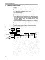
1
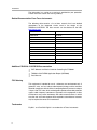
TAS5010−5112F2EVM
Evaluation Module for the TAS5010 Digital
Audio PWM Processor and the TAS5112ADFD
Digital Audio PWM Power Output Stage
User’s Guide
June 2004
DAV Digital Audio/Speaker
SLEU056
IMPORTANT NOTICE
Texas Instruments Incorporated and its subsidiaries (TI) reserve the right to make corrections, modifications,
enhancements, improvements, and other changes to its products and services at any time and to discontinue
any product or service without notice. Customers should obtain the latest relevant information before placing
orders and should verify that such information is current and complete. All products are sold subject to TI’s terms
and conditions of sale supplied at the time of order acknowledgment.
TI warrants performance of its hardware products to the specifications applicable at the time of sale in
accordance with TI’s standard warranty. Testing and other quality control techniques are used to the extent TI
deems necessary to support this warranty. Except where mandated by government requirements, testing of all
parameters of each product is not necessarily performed.
TI assumes no liability for applications assistance or customer product design. Customers are responsible for
their products and applications using TI components. To minimize the risks associated with customer products
and applications, customers should provide adequate design and operating safeguards.
TI does not warrant or represent that any license, either express or implied, is granted under any TI patent right,
copyright, mask work right, or other TI intellectual property right relating to any combination, machine, or process
in which TI products or services are used. Information published by TI regarding third-party products or services
does not constitute a license from TI to use such products or services or a warranty or endorsement thereof.
Use of such information may require a license from a third party under the patents or other intellectual property
of the third party, or a license from TI under the patents or other intellectual property of TI.
Reproduction of information in TI data books or data sheets is permissible only if reproduction is without
alteration and is accompanied by all associated warranties, conditions, limitations, and notices. Reproduction
of this information with alteration is an unfair and deceptive business practice. TI is not responsible or liable for
such altered documentation.
Resale of TI products or services with statements different from or beyond the parameters stated by TI for that
product or service voids all express and any implied warranties for the associated TI product or service and
is an unfair and deceptive business practice. TI is not responsible or liable for any such statements.
Following are URLs where you can obtain information on other Texas Instruments products and application
solutions:
Products
Amplifiers
Applications
amplifier.ti.com
Audio
www.ti.com/audio
Data Converters
dataconverter.ti.com
Automotive
www.ti.com/automotive
DSP
dsp.ti.com
Broadband
www.ti.com/broadband
Interface
interface.ti.com
Digital Control
www.ti.com/digitalcontrol
Logic
logic.ti.com
Military
www.ti.com/military
Power Mgmt
power.ti.com
Optical Networking
www.ti.com/opticalnetwork
Microcontrollers
microcontroller.ti.com
Security
www.ti.com/security
Telephony
www.ti.com/telephony
Video & Imaging
www.ti.com/video
Wireless
www.ti.com/wireless
Mailing Address:
Texas Instruments
Post Office Box 655303 Dallas, Texas 75265
Copyright © 2004, Texas Instruments Incorporated
EVM IMPORTANT NOTICE
Texas Instruments (TI) provides the enclosed product(s) under the following conditions:
This evaluation kit being sold by TI is intended for use for ENGINEERING DEVELOPMENT OR EVALUATION
PURPOSES ONLY and is not considered by TI to be fit for commercial use. As such, the goods being provided
may not be complete in terms of required design-, marketing-, and/or manufacturing-related protective
considerations, including product safety measures typically found in the end product incorporating the goods.
As a prototype, this product does not fall within the scope of the European Union directive on electromagnetic
compatibility and therefore may not meet the technical requirements of the directive.
Should this evaluation kit not meet the specifications indicated in the EVM User’s Guide, the kit may be returned
within 30 days from the date of delivery for a full refund. THE FOREGOING WARRANTY IS THE EXCLUSIVE
WARRANTY MADE BY SELLER TO BUYER AND IS IN LIEU OF ALL OTHER WARRANTIES, EXPRESSED,
IMPLIED, OR STATUTORY, INCLUDING ANY WARRANTY OF MERCHANTABILITY OR FITNESS FOR ANY
PARTICULAR PURPOSE.
The user assumes all responsibility and liability for proper and safe handling of the goods. Further, the user
indemnifies TI from all claims arising from the handling or use of the goods. Please be aware that the products
received may not be regulatory compliant or agency certified (FCC, UL, CE, etc.). Due to the open construction
of the product, it is the user’s responsibility to take any and all appropriate precautions with regard to electrostatic
discharge.
EXCEPT TO THE EXTENT OF THE INDEMNITY SET FORTH ABOVE, NEITHER PARTY SHALL BE LIABLE
TO THE OTHER FOR ANY INDIRECT, SPECIAL, INCIDENTAL, OR CONSEQUENTIAL DAMAGES.
TI currently deals with a variety of customers for products, and therefore our arrangement with the user is not
exclusive.
TI assumes no liability for applications assistance, customer product design, software performance, or
infringement of patents or services described herein.
Please read the EVM User’s Guide and, specifically, the EVM Warnings and Restrictions notice in the EVM
User’s Guide prior to handling the product. This notice contains important safety information about temperatures
and voltages. For further safety concerns, please contact the TI application engineer.
Persons handling the product must have electronics training and observe good laboratory practice standards.
No license is granted under any patent right or other intellectual property right of TI covering or relating to any
machine, process, or combination in which such TI products or services might be or are used.
Mailing Address:
Texas Instruments
Post Office Box 655303
Dallas, Texas 75265
Copyright © 2004, Texas Instruments Incorporated
EVM WARNINGS AND RESTRICTIONS
It is important to operate this EVM within the input voltage range of 0 V to 29.5 V for the output
stage and 15 V to 20 V for the system supply.
Exceeding the specified input range may cause unexpected operation and/or irreversible
damage to the EVM. If there are questions concerning the input range, please contact a TI
field representative prior to connecting the input power.
Applying loads outside of the specified output range may result in unintended operation and/or
possible permanent damage to the EVM. Please consult the EVM User’s Guide prior to
connecting any load to the EVM output. If there is uncertainty as to the load specification,
please contact a TI field representative.
During normal operation, some circuit components may have case temperatures greater than
60°C. The EVM is designed to operate properly with certain components above 60°C as long
as the input and output ranges are maintained. These components include but are not limited
to linear regulators, switching transistors, pass transistors, and current sense resistors. These
types of devices can be identified using the EVM schematic located in the EVM User’s Guide.
When placing measurement probes near these devices during operation, please be aware
that these devices may be very warm to the touch.
Mailing Address:
Texas Instruments
Post Office Box 655303
Dallas, Texas 75265
Copyright © 2004, Texas Instruments Incorporated
Information About Cautions and Warnings
Preface
Read This First
About This Manual
This manual describes the operation of the TAS5010−5112F2EVM evaluation
module from Texas Instruments.
How to Use This Manual
This document contains the following chapters:
- Chapter 1 – Overview
- Chapter 2 – Detailed Description of the EVM Board
- Chapter 3 – EVM Board Operation
- Chapter 4 – Hints for Measurements of Performance
Information About Cautions and Warnings
This book may contain cautions and warnings.
This is an example of a caution statement.
A caution statement describes a situation that could potentially
damage your software or equipment.
This is an example of a warning statement.
A warning statement describes a situation that could potentially
cause harm to you.
iii
Trademarks
The information in a caution or a warning is provided for your protection.
Please read each caution and warning carefully.
Related Documentation From Texas Instruments
The following table contains a list of data manuals that have detailed
descriptions of the integrated circuits used in the design of the
TAS5010−5112F2EVM. The data manuals can be obtained at the URL
http://www.ti.com.
Part Number
Literature Number
TAS5010PFB
SLAS328
TAS5112ADFD
SLES094
TAS3002PFB
SLAS307
DIR1703E
SLES007
LMV331IDBVR
SLCS136
TPS3705−33DGN
SLVS184
SN74LVC2GU04DBVR
SCES197
SN74LVC2G14DBVR
SCES200
SN74LVC2G08DCTR
SCES198
SN74LVC1G02DBVR
SCES213
SN74LVC1G32DBVR
SCES219
SN74LV21APWR
SCES340
Additional TAS5010−5112F2EVM Documentation
- DCT Software and User’s Guide for Controlling the TAS3002
- TAS5010−5112F2EVM Application Report (SLEA036)
- Data Manuals
FCC Warning
This equipment is intended for use in a laboratory test environment only. It
generates, uses, and can radiate radio frequency energy and has not been
tested for compliance with the limits of computing devices pursuant to subpart
J of part 15 of FCC rules, which are designed to provide reasonable protection
against radio frequency interference. Operation of this equipment in other
environments may cause interference with radio communications, in which
case the user at his own expense will be required to take whatever measures
may be required to correct this interference.
Trademarks
Equibit™ and PurePath Digital™ are trademarks of Texas Instruments.
iv
Contents
Contents
1
Introduction . . . . . . . . . . . . . . . . . . . . . . . . . . . . . . . . . . . . . . . . . . . . . . . . . . . . . . . . . . . . . . . . . . . . . 1-1
1.1
TAS5010−5112F2EVM Features . . . . . . . . . . . . . . . . . . . . . . . . . . . . . . . . . . . . . . . . . . . . . . 1-2
2
Detailed Description of the EVM . . . . . . . . . . . . . . . . . . . . . . . . . . . . . . . . . . . . . . . . . . . . . . . . . .
2.1
Board Overview . . . . . . . . . . . . . . . . . . . . . . . . . . . . . . . . . . . . . . . . . . . . . . . . . . . . . . . . . . . .
2.2
Description of Jumper Settings . . . . . . . . . . . . . . . . . . . . . . . . . . . . . . . . . . . . . . . . . . . . . . .
2.2.1 Double-Speed Control (JMP120) . . . . . . . . . . . . . . . . . . . . . . . . . . . . . . . . . . . . . .
2.2.2 Enable/Disable S/PDIF−MUTE (JMP130) . . . . . . . . . . . . . . . . . . . . . . . . . . . . . . .
2.2.3 Bypassing Equalizer Functions in the Digital Audio Processor (JMP360) . . . .
2.3
Default Jumper Positioins . . . . . . . . . . . . . . . . . . . . . . . . . . . . . . . . . . . . . . . . . . . . . . . . . . . .
2.4
Description of Connectors . . . . . . . . . . . . . . . . . . . . . . . . . . . . . . . . . . . . . . . . . . . . . . . . . . .
2.4.1 S/PDIF Digital Audio Coaxial/RCA Input (J100) . . . . . . . . . . . . . . . . . . . . . . . . . .
2.4.2 S/PDIF Optical (J101) . . . . . . . . . . . . . . . . . . . . . . . . . . . . . . . . . . . . . . . . . . . . . . . .
2.4.3 Analog input (J160) and Analog Output (J170) . . . . . . . . . . . . . . . . . . . . . . . . . .
2.4.4 PC and I2C Interface (J300) . . . . . . . . . . . . . . . . . . . . . . . . . . . . . . . . . . . . . . . . . . .
2.4.5 Loudspeaker Connectors (J540, J541, J580, and J581) . . . . . . . . . . . . . . . . . .
2.4.6 Power Supply Connector . . . . . . . . . . . . . . . . . . . . . . . . . . . . . . . . . . . . . . . . . . . . .
2.5
Description of Switches and Buttons . . . . . . . . . . . . . . . . . . . . . . . . . . . . . . . . . . . . . . . . . .
2.5.1 S/PDIF Input Selector Switch (S100) . . . . . . . . . . . . . . . . . . . . . . . . . . . . . . . . . . .
2.5.2 Bypass Digital Audio Processor Switch (S320) . . . . . . . . . . . . . . . . . . . . . . . . . .
2.5.3 Reset Board Button (S620) . . . . . . . . . . . . . . . . . . . . . . . . . . . . . . . . . . . . . . . . . . .
2.5.4 Mute Button (S240) . . . . . . . . . . . . . . . . . . . . . . . . . . . . . . . . . . . . . . . . . . . . . . . . . .
2.5.5 Volume Control (S340 and S341) . . . . . . . . . . . . . . . . . . . . . . . . . . . . . . . . . . . . . .
2.6
Description of Indicators . . . . . . . . . . . . . . . . . . . . . . . . . . . . . . . . . . . . . . . . . . . . . . . . . . . . .
2.6.1 Power LED (LED223) . . . . . . . . . . . . . . . . . . . . . . . . . . . . . . . . . . . . . . . . . . . . . . . .
2.6.2 No S/PDIF Input LED (LED222) . . . . . . . . . . . . . . . . . . . . . . . . . . . . . . . . . . . . . . .
2.6.3 Temperature Warning LED (LED221) . . . . . . . . . . . . . . . . . . . . . . . . . . . . . . . . . .
2.6.4 Protection Mode LED (LED220) . . . . . . . . . . . . . . . . . . . . . . . . . . . . . . . . . . . . . . .
2-1
2-2
2-3
2-3
2-3
2-3
2-4
2-4
2-4
2-4
2-4
2-5
2-6
2-6
2-7
2-7
2-7
2-7
2-7
2-7
2-8
2-8
2-8
2-8
2-8
3
EVM Board Operation . . . . . . . . . . . . . . . . . . . . . . . . . . . . . . . . . . . . . . . . . . . . . . . . . . . . . . . . . . . .
3.1
Power Supply . . . . . . . . . . . . . . . . . . . . . . . . . . . . . . . . . . . . . . . . . . . . . . . . . . . . . . . . . . . . . .
3.1.1 Power the EVM by One Power Supply . . . . . . . . . . . . . . . . . . . . . . . . . . . . . . . . .
3.1.2 Power the EVM With Two Power Supplies . . . . . . . . . . . . . . . . . . . . . . . . . . . . . .
3.2
Setup the TAS5010−5112F2EVM With the S/PDIF Input . . . . . . . . . . . . . . . . . . . . . . . . .
3.2.1 Start-up Sequence . . . . . . . . . . . . . . . . . . . . . . . . . . . . . . . . . . . . . . . . . . . . . . . . . . .
3.3
Setup the TAS5010−5112F2EVM With the Analog Line Input . . . . . . . . . . . . . . . . . . . . .
3.4
Interfacing the Analog Line Output . . . . . . . . . . . . . . . . . . . . . . . . . . . . . . . . . . . . . . . . . . . .
3.5
Controlling the DAP With PC Software . . . . . . . . . . . . . . . . . . . . . . . . . . . . . . . . . . . . . . . .
3-1
3-2
3-2
3-2
3-3
3-4
3-4
3-4
3-4
4
Hints for Measurement of Performance . . . . . . . . . . . . . . . . . . . . . . . . . . . . . . . . . . . . . . . . . . . 4-1
v
Contents
Figures
1−1
2−1
2−2
2−3
2−4
2−5
2−6
3−1
3−2
Simplified TAS5010−5112F2EVM Block Diagram . . . . . . . . . . . . . . . . . . . . . . . . . . . . . . . . . .
Board Outline With Connectors, Switches, Jumpers, and Indicators . . . . . . . . . . . . . . . . . .
Physical Structure for the TAS5010−5112F2EVM . . . . . . . . . . . . . . . . . . . . . . . . . . . . . . . . . .
Default Jumper Positions . . . . . . . . . . . . . . . . . . . . . . . . . . . . . . . . . . . . . . . . . . . . . . . . . . . . . . .
Pin Numbers at the Line Input/Output Connector (Top View) . . . . . . . . . . . . . . . . . . . . . . . .
Pin Numbers at the Parallel Port/I2C Interface/I2C (J300) . . . . . . . . . . . . . . . . . . . . . . . . . . .
Pin Numbers at PSU Connector (Top View) . . . . . . . . . . . . . . . . . . . . . . . . . . . . . . . . . . . . . . .
Recommended Power-Up and Power-Down Sequence . . . . . . . . . . . . . . . . . . . . . . . . . . . .
EVM Board Connected to S/PDIF Sources and Personal Computer . . . . . . . . . . . . . . . . .
1-2
2-2
2-2
2-4
2-4
2-5
2-6
3-2
3-3
Tables
2−1
2−2
2−3
2−4
3−1
3−2
vi
Description of J160 and J170 . . . . . . . . . . . . . . . . . . . . . . . . . . . . . . . . . . . . . . . . . . . . . . . . . . .
Description of J300 . . . . . . . . . . . . . . . . . . . . . . . . . . . . . . . . . . . . . . . . . . . . . . . . . . . . . . . . . . . .
Description of Loudspeaker Connectors . . . . . . . . . . . . . . . . . . . . . . . . . . . . . . . . . . . . . . . . . .
Description of PSU Connector . . . . . . . . . . . . . . . . . . . . . . . . . . . . . . . . . . . . . . . . . . . . . . . . . .
Maximum Supply Voltage (Single Supply) . . . . . . . . . . . . . . . . . . . . . . . . . . . . . . . . . . . . . . . .
Maximum H-bridge Voltage vs Load Impedance . . . . . . . . . . . . . . . . . . . . . . . . . . . . . . . . . . .
2-5
2-5
2-6
2-6
3-2
3-2
Chapter 1
Introduction
The TAS5010−5112F2EVM PurePath Digitalt customer evaluation module
demonstrates two integrated circuits, the TAS5010 and TAS5112ADFD from
Texas Instruments. The TAS5010 is a high performance 24-bit stereo digital
modulator based on Equibitt technology. This IC converts input PCM serial
digital audio data to a pulse width modulated (PWM) audio data stream. The
TAS5010 PWM modulator accepts I2S data with a sample rate up to 192 kHz.
The TAS5010 is designed for implementation together with the
TAS5112ADFD digital output stage for driving two loudspeakers in a stereo
application.
The TAS5010 is pin compatible with the TAS5001 PCM−PWM modulator. The
maximum sample rate for the TAS5001 is 96 kHz.
Together, the TAS5010 and one TAS5112ADFD provide the complete
PurePath Digitalt conversion of a 3.3-V digital audio input stream up to
2x50 W into 6-Ω loudspeakers. The chipset is ideal for applications requiring
excellent audio quality, minimum size and weight, and high power efficiency.
The chipset can be used in a range of products such as micro-components
systems, home theater in a box, DVD receivers, or TV sets.
The TAS5010−5112F2EVM is a complete true digital amplifier including an
S/DIF receiver, I2S audio interface, volume control, interface to personal
computer through the parallel port, and required control logic. The amplifier
reference design is surrounded by a white line on the PCB.
Topic
1.1
Page
TAS5010−5112F2EVM Features . . . . . . . . . . . . . . . . . . . . . . . . . . . . . . . . . 1-2
Introduction
1-1
TAS5010−5112F2EVM Features
1.1 TAS5010−5112F2EVM Features
- PurePath Digital™ reference design (double-sided plated-through PCB
layout)
- S/PDIF receiver with coaxial and optical input (sampling rate = 32 kHz –
192 kHz)
- I2S audio interface (sampling rate: 32 kHz – 96 kHz)
- On-board volume control
- Auto-mute function
- Self-contained short circuit and temperature protection system
- Digital audio processor (DAP), which include 24-bit volume control, digital
gain, bass and treble control, parametric equalization, dedicated speaker
equalization, loudness control, and adjustable dynamic range
compression/expansion.
- DAP control through PC software (DCT software from Texas Instruments)
- Default DAP settings is downloaded to an EEPROM with the DCT
software
- Analog line input (use internal analog-to-digital converter in DAP)
- Analog line output (use internal digital-to-analog converter in DAP)
Figure 1−1. Simplified TAS5010−5112F2EVM Block Diagram
PC SOFTWARE
PARRALLEL
PORT
INTERFACE
VOLUME
CONTROL
I2C BUS
TAS3002
DIGITAL AUDIO
PROCESSOR
ANALOG INPUT
ANALOG OUTPUT
OPTICAL INPUT
32 kHz − 96 kHz
COAXIAL INPUT
I2S INPUT
32 kHz − 192 kHz
DIR1703
S/PDIF
RECEIVER
I2S INTERFACE
I2S BUS
TAS5010
DIGITAL AUDIO
PWM PROCESSOR
TAS5112ADFD
DIGITAL AUDIO
PWM POWER
OUTPUT STAGE
I2S BUS
The DIR1703 IC from Texas Instruments/Burr-Brown is used as S/PDIF
receiver and system clock generator. This product is a digital audio interface
receiver (DIR) that receives and decodes audio data up to 96-kHz sampling
rate. DIR1703 is running in a configuration where it automatically switches
between PLL mode and crystal mode. When the DIR1703 is connected to an
active digital source, it is running in PLL-mode. The system clock (SCKO)
frequency depends on the incoming sampling rate (fs): SCKO = 256 x fs. When
no digital source is represented, the DIR1703 switches to crystal mode. The
system clock frequency in crystal mode depends on the external crystal
connected to the DIR1703 receiver. On the TAS5010−5112F2EVM board, the
crystal-mode system clock is 12.288 MHz.
Crystal-mode operation is used to generate a fixed clock when the
TAS5010−5112F2EVM board is connected to an analog source. The external
anti-aliasing filter for the A/D converter is optimized to 48-kHz sampling rates.
1-2
TAS5010−5112F2EVM Features
The TAS3002 IC from Texas Instruments is used as digital audio processor
(DAP). All features in the DAP can be controlled through the I2S interface.
Adjustment of the sound level can be executed through the I2C bus and with
two push buttons on the EVM board.
During power up, the TAS3002 settings and coefficients are loaded from an
external serial EEPROM. The TAS3002 coefficients control all features in the
DAP. Customized start up settings can be downloaded to the EEPROM. This
operation is easy to execute with a personal computer, DCT software, and a
cable between TAS5010−5112F2EVM and the computer. The
TAS5010−5112F2EVM is connected to the LPT port at the computer.
Introduction
1-3
1-4
Chapter 2
Detailed Description of the EVM
This chapter describes the TAS5010−5112F2EVM board in regards to board
layout, jumpers, switches, buttons, and connectors.
Topic
Page
2.1
Board Overview . . . . . . . . . . . . . . . . . . . . . . . . . . . . . . . . . . . . . . . . . . . . . . . 2-2
2.2
Description of Jumper Settings . . . . . . . . . . . . . . . . . . . . . . . . . . . . . . . . 2-3
2.3
Default Jumper Positioins . . . . . . . . . . . . . . . . . . . . . . . . . . . . . . . . . . . . . 2-4
2.4
Description of Connectors . . . . . . . . . . . . . . . . . . . . . . . . . . . . . . . . . . . . . 2-4
2.5
Description of Switches and Buttons . . . . . . . . . . . . . . . . . . . . . . . . . . . 2-7
2.6
Description of Indicators . . . . . . . . . . . . . . . . . . . . . . . . . . . . . . . . . . . . . . 2-8
Detailed Description of the EVM
2-1
Board Overview
2.1 Board Overview
Figure 2−1. Board Outline With Connectors, Switches, Jumpers, and Indicators
PSU Connector
J600
J100
S620
*
J101
−
+
Volume Control
+
J581
−
Speaker Right
LED220
S340
LED221
S341
PROTECTION MODE
J400
TEMPERATURE WARNING
BYPASSED
J300
LED223
S32
0
EQ ENABLE
*
JMP360
EQ DISABLE
EQUALIZER ENABLE
PC and I 2C Connector
J580
BYPASS DIGITAL AUDIO PROCESSOR
ACTIVE
LED222
J160
−
MUTE
POWER
D/A−Converter Input
J541
S240
I2S Interface
J170
+
SAMPLE RATE
CONTROL
*****
A/D−Converter Output
*
J540
RESET
Speaker Left
Optical
S/PDIF Digital Audio
Optical/Toslink Input
S/PDIF ERROR
ENABLE
JMP120
S10
0
Switch between Optical
and Coaxial input
JMP130
Coaxial
NO S/PDIF
S/PDIF Digital Audio
Coaxial/RCA Input
Note: *) Indicates default jumper posistions.
The physical structure for the TAS5010−5112F2EVM is illustrated in
Figure 2−2. Block headings refer to page headings in the
TAS5010−5112F2EVM schematic.
Figure 2−2. Physical Structure for the TAS5010−5112F2EVM
POWER SUPPPLY SECTION
AUDIO INPUT SECTION
CONTROL SECTION
TAS5010 + TAS5112ADFD REFERENCE DESIGN
PCM TO PWM MODULATOR SECTION & OUTPUT STAGE SECTION
DIGITAL AUDIO
PROCESSOR SECTION
2-2
Description of Jumper Settings
2.2 Description of Jumper Settings
There are three jumpers on the EVM board (J400 is an I2S interface)
2.2.1
Double-Speed Control (JMP120)
JMP120 is used to set the double-speed pin at TAS5010 (DBSPD, pin 39). The
TAS5010 is operating in single-speed mode if the DBSPD pin is asserted low
and in double-speed if it is asserted high. Single-speed is required for
sampling rate at 32 kHz, 44.1 kHz, 48 kHz, and double-speed for 88-kHz and
96-kHz sampling rate.
The S/PDIF receiver automatically controls the DBSPD pin if JMP120 shunts
pin 1 and 2 (default setting). If JMP120 shunts pin 2 and 3, the TAS5010 is in
single-speed mode. If JMP120 shunts pin 3 and 4, the TAS5010 is in double
speed mode.
2.2.2
Enable/Disable S/PDIF−MUTE (JMP130)
JMP130 is used to disable the S/PDIF-MUTE signal (S/PDIF-MUTE =
(DIR1703-UNLOCK + DIR1703-ADFLG)). The DIR1703-UNLOCK signal is
high until the PLL in DIR1703 detects and locks on an incoming digital signal.
The ADFLG signal is high when the S/PDIF data does not include a PCM audio
signal.
The S/PDIF-MUTE signal is used to shutdown the output stage (the H-bridge
stop switching). To obtain click and pop reduced shutdown it is necessary to
mute the output stage before Reset on TAS5010 is asserted low.
When the EVM board is connected to an analog source or to a digital source
through the I2S interface, is it necessary to disable the UNLOCK warning. This
is done with the JMP130 jumper. When JMP130 shunts pin 1 and 2 the
UNLOCK warning is enabled (default setting). The warning signal is disabled
If JMP130 shunts pin 2 and 3.
2.2.3
Bypassing Equalizer Functions in the Digital Audio Processor (JMP360)
JMP360 is used to disable the equalizer function in the DAP. The equalizer
function is enabled if JMP360 shunts pin 1 and 2. The equalizer is disabled
when JMP360 shunts pin 2 and 3.
Note:
Bass and treble are flat when the equalizer is bypassed.
Detailed Description of the EVM
2-3
Default Jumper Positioins
2.3 Default Jumper Positioins
Default jumper positions are marked with a grey rectangle in Figure 2−3.
Figure 2−3. Default Jumper Positions
J600
J100
J540
+
J541
−
J580
+
J581
−
JMP130
JMP120
J101
J170
J160
JMP360
J300
2.4 Description of Connectors
2.4.1
S/PDIF Digital Audio Coaxial/RCA Input (J100)
The RCA connector can be connected to a digital S/PDIF source through a
coaxial cable with 75-Ω characteristic impedance (e.g., RG59 cable). The
highest sampling rate supported for this input is 96 kHz.
2.4.2
S/PDIF Optical (J101)
The Toslink connector can be connected to a digital S/PDIF signal through an
optical cable. The highest sampling rate supported for this input is 96 kHz.
2.4.3
Analog input (J160) and Analog Output (J170)
Analog sources can be connected to the A/D converter through J160. The
analog line input is optimized for an input signal with a maximum voltage at
2.1 VRMS.
Analog output from the digital audio processor is available at P170. Maximum
output level is 0.7 VRMS. Pin numbers for J170 is equal to numbers at J160
Figure 2−4. Pin Numbers at the Line Input/Output Connector (Top View)
3
2
1
2-4
Description of Connectors
Table 2−1. Description of J160 and J170
Pin No.
Description
Analog Input Connector (J160)
1
Left Channel Input
2
Ground
3
Right Channel Input
Analog Output Connector (J170)
2.4.4
1
Left Channel output
2
Ground
3
Right Channel Output
PC and I2C Interface (J300)
The PC interface using the attached special cable to parallel/printer port on the
PC. This makes it possible to control the TAS3002 digital audio processor
totally from the PC using the special DCT software saved on the PurePath
Digitalt amplifier CD-ROM.
The PC interface can also be used to control the TAS3002 from an external
microcontroller of your own choice.
Figure 2−5. Pin Numbers at the Parallel Port/I 2C Interface/I 2C (J300)
9
6
8
5 4
7
3
2 1
Table 2−2. Description of J300
Pin No.
Pin Description
I/O
Net Name on Schematic
1
Power ON Reset
O
POWER−ON−RESET
2
Serial Data Line (SDA)
I/O
SDA−BI
3
Serial Clock Line (SCL)
I/O
SCL−BI
4
Serial Data Line In
I
SDA−IN
5
Serial Clock Line Out
O
SCL−OUT
6
Reserved
−
For future use
7
Serial Data Line Out
O
SDA−OUT
8
Serial Clock Line In
I
SCL−IN
9
0V
−
GND
Pin 2 (SDA) and pin 3 (SCL) are used for communication between an external
micro-controller and the digital audio processor.
Detailed Description of the EVM
2-5
Description of Connectors
2.4.5
Loudspeaker Connectors (J540, J541, J580, and J581)
All speaker connectors accept standard 4 mm plugs. Use of high quality plugs
and speaker cable are recommended.
Table 2−3. Description of Loudspeaker Connectors
Reference Designator
Description
J540
Left speaker positive output terminal
J541
Left speaker negative output terminal
J580
Right speaker positive output terminal
J581
Right speaker negative output terminal
Caution
Both positive and negative speaker outputs are floating and may NOT
be connected to ground (f.ex. through an oscilloscope).
2.4.6
Power Supply Connector
Figure 2−6. Pin Numbers at PSU Connector (Top View)
4
3
2
1
Table 2−4. Description of PSU Connector
Pin No.
2-6
Description
Net Name at Schematic
1
Supply voltage for output stage
(VHBR)
POWER−OUTPUT−STAGE
2
Supply voltage for control and gate
drive (V+)
−
3
Ground
GND
4
Ground
GND
Description of Switches and Buttons
2.5 Description of Switches and Buttons
2.5.1
S/PDIF Input Selector Switch (S100)
S100 switches between optical and coaxial S/PDIF input. When the lever is
pressed in the direction of J101, the optical S/PDIF input is selected. When the
lever is pressed in the direction of J100, the coaxial S/PDIF input is selected.
2.5.2
Bypass Digital Audio Processor Switch (S320)
When the lever is pressed in the direction of S341, the DAP is bypassed. When
the lever is pressed in the direction of U360 (TAS3002), the DAP is in the signal
path. Below S320 is a label (DAP ON), which indicates the position of the lever
for the DAP inserted in signal path.
Warning
Bypassing the DAP is equal to maximum output power (attenuation = 0 dB). This
might be loud and could possible damage your loudspeaker and hearing.
2.5.3
Reset Board Button (S620)
This is the master RESET for the EVM board. While this button is held down,
the DIR1703, TAS3002, TAS5010, and TAS5112ADFD are held RESET and
latching errors are cleared. Note that while the RESET button is held down,
the No S/PDIF LED lights up, even if a valid S/PDIF input signal is present,
because the DIR1703 S/PDIF receiver is held RESET.
2.5.4
Mute Button (S240)
The output stage is muted (not switching) while this button is held down and
unmutes when it is released.
2.5.5
Volume Control (S340 and S341)
S341 and S340: Volume control of TAS3002 DAP. Press and hold the S341
button to decrease output power level. Press and hold the S340 button to
increase output power level.
Note:
Change of listening level is slow. It takes approximately 25 seconds to
change attenuation from –70 dB to 0 dB.
The TAS3002 device implements a soft volume control. This feature allows a
change from one volume level to another over the entire range of volume
control (+18 dB to mute). Above 0 dB, there is risk of signal clipping. Distortion
of output signals is the result of signal clipping.
Note:
Significant signal clipping might result in activation of the overcurrent
protection system.
Detailed Description of the EVM
2-7
Description of Indicators
2.6 Description of Indicators
2.6.1
Power LED (LED223)
The green LED indicates that the
TAS5010−5112F2EVM board is powered on.
2.6.2
control
circuitry
at
the
No S/PDIF Input LED (LED222)
The yellow LED indicates that the S/PDIF input signal is missing or it does not
contain valid audio data.
Reasons to have a No S/PDIF warning:
- The lever at the S/PDIF input selector switch (S100) is placed in the wrong
position.
- The S/PDIF signal is missing. Some DVD players remove the S/PDIF
output signal when the drawer is opened.
Note:
When the SPDIF−MUTE signal from the S/PDIF receiver is disabled
(JMP130 is shunting pin 2 and pin 3), the No S/PDIF indication is disabled.
2.6.3
Temperature Warning LED (LED221)
The yellow LED indicates that the temperature of the TAS5112ADFD junction
has reached the warning level. This is step one of the two-step thermal
protection system implemented in the TAS5112ADFD device. The
temperature warning is an indication only; the operation of the system is
unchanged. If the temperature increases further and above the shutdown
level, the error latch is set and the system goes into RESET mode. At this point,
the Protection Mode LED will be lit as well as the Temperature Warning LED.
2.6.4
Protection Mode LED (LED220)
The red LED indicates that protection circuit is engaged and it has put the
output stage in shutdown mode.
Possible causes for shutdown mode:
- Two speaker terminals are shorted
- The amplifier is constantly overloaded (decrease volume level).
- One speaker terminal is shorted to ground (f.ex. through an oscilloscope)
- The output stage is in thermal shutdown due to overload.
Check the setup and board carefully and remove the cause of the failure before
pressing RESET (S620) to disengage the protection mode.
2-8
Chapter 3
EVM Board Operation
This chapter describes the TAS5010−5112F2EVM board operation.
Topic
Page
3.1
Power Supply . . . . . . . . . . . . . . . . . . . . . . . . . . . . . . . . . . . . . . . . . . . . . . . . . 3-2
3.2
Setup the TAS5010-5112F2EVM With the S/PDIF Input . . . . . . . . . . . . 3-3
3.3
Setup the TAS5010-5112F2EVM With the Analog Line Input . . . . . . . 3-4
3.4
Interfacing the Analog Line Output . . . . . . . . . . . . . . . . . . . . . . . . . . . . . 3-4
3.5
Controlling the DAP With PC Software . . . . . . . . . . . . . . . . . . . . . . . . . . 3-4
EVM Board Operation
3-1
Power Supply
3.1 Power Supply
The TAS5010−5112F2EVM can be powered from one or two external power
supplies. High-end audio performance requires a stabilized power supply with
low ripple voltage and low output impedance.
Note:
The length of the power supply cable must be minimized. Increasing the
length of the PSU cable is equal to increasing the distortion for the amplifier
at high output levels and low frequencies.
3.1.1
Power the EVM by One Power Supply
A single power supply can be connected to the TAS5010−5112F2EVM board.
Short VHBR and V+ at the power cable (red and white plugs).
Voltage for the connected power supply is not allowed to be below 15 V. The
maximum supply voltage depends of the speaker load resistance. Check the
recommended maximum supply voltage in the TAS5112ADFD data sheet
(SLES094).
Table 3−1. Maximum Supply Voltage (Single Supply)
RLOAD = 6 Ω
Supply voltage (VHBR and V+)
3.1.2
29.5 V
Power the EVM With Two Power Supplies
When two supplies power the TAS5010−5112F2EVM, it is possible to adjust
the output power with the level of the voltage VHBR (pin 1 at J640). The
minimum VHBR voltage is 0 V. The maximum voltage depends of the load
resistance. Check the recommended maximum supply voltage in the
TAS5112ADFD data sheet (SLES094).
Table 3−2. Maximum H-bridge Voltage vs Load Impedance
RLOAD = 6 Ω
29.5 V
Maximum VHBR voltage
15 V – 20 V
V+ voltage
Figure 3−1. Recommended Power-Up and Power-Down Sequence
V+
VHBR
>1 ms
3-2
>1 ms
Setup the TAS5010−5112F2EVM With the S/PDIF Input
3.2 Setup the TAS5010−5112F2EVM With the S/PDIF Input
Connect the EVM board as shown in Figure 3−2. Select between coaxial or
optical input signal at the input selector switch (S100).
Press the lever at S320 in the direction of U360 if the TAS3002 DAP is wanted
in the signal path (recommended during normal listening tests). There is no
attenuation if DAP is bypassed. If the DAP is in the signal path, the start-up
volume level depends on what is programmed in the serial EEPROM on the
EVM board. The default startup volume level is initially programmed to 12 dB
below full scale, which on some speakers still might be loud. The default
volume level can be changed with the DCT software on the PC.
The following are the conditions for standard setup:
1) All jumpers are in default position.
2) Speakers, power supply, and if required a cable for PC communication are
initially connected to the EVM board.
3) The TAS5010−5112F2EVM can be powered with either one or two power
supplies (see the Power Supply section). Power supplies are initially
switched OFF.
4) Music player is initially switched OFF.
5) PC connection is optional.
Figure 3−2. EVM Board Connected to S/PDIF Sources and Personal Computer
Power
Supply
Power
Supply
S/PDIF Coaxial/RCA cable
PSU Connector
S/PDIF ERROR
ENABLE
*
*
J101
J170
JMP120
S100
Optical
J540
GREEN
RESET
S240
J541
MUTE
BLUE
J160
+
SAMPLE RATE
CONTROL
−
SPEAKER LEFT
PC with GUI software to control:
− Volume
− Bass, Treble & Loudness
− Equalizer
− Loudness
S341
S340
−
+
VOLUME CONTROL
POWER
LED220
Attached cable for PC
Interface (LPT Port)
LED221
J400
J300
LED222
BYPASSED
J580
GREEN
LED223
EQ ENABLE *
*****
EQUALIZER ENABLE
S320
EQ DISABLE
JMP360
BYPASS DIGITAL AUDIO PROCESSOR
ACTIVE
I2S Interface
S/PDIF Optical/Toslink cable
JMP130
Coaxial
Switch between
Optical and Coaxial input
GND
GND
S620
V+
VHBR
J600
J100
+
J581
BLUE
−
SPEAKER RIGHT
Note: *) Indicates default jumper posistions.
NO S/PDIF
TEMPERATURE WARNING
PROTECTION MODE
EVM Board Operation
3-3
Setup the TAS5010−5112F2EVM With the Analog Line Input
3.2.1
Start-up Sequence
1) Turn on the power supply/supplies. Follow the power-up and power-down
sequence described in the Power Supply section. Observe that the green
Power ON LED and the yellow No S/PDIF LED are lit.
2) Run the DCT software from the PC desktop if the DAP is activated (S320)
and the attached cable is connected from J300 to the PC.
3) Turn on the CD/DVD player and play the test CD. Observe that the yellow
No S/PDIF now is OFF.
4) Observe that digital audio is coming from the left and right speakers.
3.3 Setup the TAS5010−5112F2EVM With the Analog Line Input
- Disable the UNLOCK warning from S/PDIF receiver (JMP130: shunts pin
2 and 3)
- Connect the TAS5010−5112F2EVM board and PC with the attached cable
- Connect the analog source to the analog input (J160)
- Power up the TAS5010−5112F2EVM board
- Enable the TAS3002 analog input with the DCT software
- Disable the TAS3002 digital input (both SDIN1 and SDIN2) with the DCT
software
- The TAS5010−5112F2EVM board is ready to play with analog source
3.4 Interfacing the Analog Line Output
The default is the analog line output (J170) active. The analog line output can
be connected to analog tape recorders or analog amplifiers (e.g., a
subwoofer).
3.5 Controlling the DAP With PC Software
Operating instructions for the DCT software are described in the Digital Audio
Processor (DAP) Configuration Tool Operating Instruction user’s guide, which
is located on the PurePath Digitalt Amplifier CD-ROM.
3-4
Chapter 4
Hints for Measurement of Performance
Read the Digital Audio Measurements application note (SLAA114) for an
introduction to measurements on true digital audio amplifiers.
You are welcome to use the audio precision test files available on the PurePath
Digital™ amplifier CD-ROM. Note that an AES17 filter is required to reach the
shown measurements. Specifications for the AES17 filter are described in the
AES Standard Method For Digital Audio Engineering – Measurement of Digital
Audio Equipment (the AES17 standard is available from the Audio
Engineering Society – www.aes.org).
When evaluating the performance of the digital amplifier section, bypass the
digital audio processor with S320 or adjust all settings to neutral and
attenuation to 0 dB.
Connect the TAS5010−5112F2EVM to a regulated power supply with a short
cable. The length of the PSU cable must not exceed 0,3 meters.
Hints for Measurement of Performance
4-1
4-2