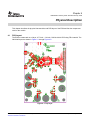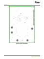
1
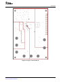
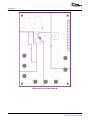
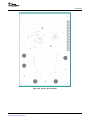
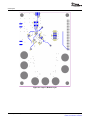
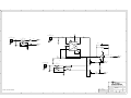
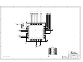
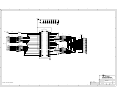
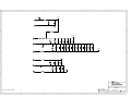
ADS5423/24/33 and ADS5411 EVM
User Guide
User's Guide
February 2006
SLWU020B
2
SLWU020B – February 2005 – Revised February 2006
Submit Documentation Feedback
Contents
1
Overview
................................................................................................................... 5
1.1
Purpose .............................................................................................................. 5
1.2
EVM Basic Functions............................................................................................... 5
1.3
Power Requirements ............................................................................................... 5
1.4
EVM Operational Procedure
1.3.1
2
Voltage Limits .............................................................................................. 5
Circuit Description
......................................................................................
5
..................................................................................................... 7
2.1
Schematic Diagram ................................................................................................. 7
2.2
Circuit Function
7
2.2.1
7
2.2.2
2.2.3
.....................................................................................................
Analog Inputs ..............................................................................................
Power ........................................................................................................
Outputs ......................................................................................................
Parts List
4
Physical Description
4.2
7
.................................................................................................................. 9
3
4.1
7
................................................................................................. 11
........................................................................................................ 11
Schematics ......................................................................................................... 17
PCB Layout
SLWU020B – February 2005 – Revised February 2006
Submit Documentation Feedback
Contents
3
List of Figures
4-1
4-2
4-3
4-4
4-5
4-6
Top Layer....................................................................................................................
Layer 2, Ground Plane ....................................................................................................
Layer 3, Power Plane #1 ..................................................................................................
Layer 4, Power Plane #2 ..................................................................................................
Layer 5, Ground Plane ....................................................................................................
Layer 6, Bottom Layer ....................................................................................................
11
12
13
14
15
16
List of Tables
1-1
2-1
2-2
3-1
4
Three Pin Jumper List Table ...............................................................................................
Output Connector J9 ........................................................................................................
Test Point Description .......................................................................................................
Bill of Materials for EVM ....................................................................................................
List of Figures
6
8
8
9
SLWU020B – February 2005 – Revised February 2006
Submit Documentation Feedback
Chapter 1
SLWU020B – February 2005 – Revised February 2006
Overview
This User’s Guide document gives a general overview of the ADS5423/24/33 and ADS5411 evaluation
module (EVM) and provides a general description of the features and functions to be considered while
using this module.
1.1
Purpose
The EVM provides a platform for evaluating the ADS5423/24/33 14-bit analog-to-digital converter (ADC)
under various signals, references, and supply conditions. This evaluation module also allows the
evaluation of the ADS5411, an 11-bit analog-to-digital converter. This document should be used in
combination with the EVM schematic diagram supplied.
1.2
EVM Basic Functions
Analog input to the ADC is provided via external SMA connectors. The single-ended input the user
provides is converted into a differential signal at the input of the device. One input path uses a differential
amplifier, while the other input is transformer coupled.
The EVM provides an external SMA connector for input of the ADC clock. The single-ended input the user
provides is converted into a differential signal at the input of the device.
Digital output from the EVM is via a 40-pin connector. The digital outputs from the ADC are buffered
before going to the connector.
Power connections to the EVM are via banana jack sockets. Separate sockets are provided for the ADC
analog and digital supplies, the external buffer supply, and the differential amplifier supply.
1.3
Power Requirements
The EVM can be powered directly with only two supplies: a 3.3-V supply for the ADC digital driver supply
and external buffer supply, and 5 V for the ADC analog supply if using the EVM with transformer coupled
analog inputs. If using the differential amplifier analog inputs, ±5 V is required. Provision has also been
made to allow the EVM to be powered with independent 3.3-V supplies to provide higher performance.
1.3.1 Voltage Limits
Exceeding the maximum input voltages can damage EVM components. Under voltage may cause
improper operation of some or all of the EVM components.
1.4
EVM Operational Procedure
The EVM provides a flexible means of evaluating the ADS5423/24/33 or ADS5411 in a number of modes
of operation. A basic setup procedure that can be used as a board confidence check is as follows:
1. Verify all jumper settings against the schematic jumper list in Table 1-1.
SLWU020B – February 2005 – Revised February 2006
Submit Documentation Feedback
Overview
5
www.ti.com
EVM Operational Procedure
Table 1-1. Three Pin Jumper List Table
JUMPER
FUNCTION
LOCATION: PINS 1–2
LOCATION: PINS 2–3
DEFAULT
Source provided from Diff Amp
1–2
SJP3
Provides AIN+ source to ADC
device
Source provided from T2
SJP4
Provides AIN– source to ADC
device
Source provided from Diff Amp Source provided from T2
2-3
2. Connect supplies to the EVM as follows:
+5 V (4.75 V–5.25 V) ADC analog supply to J3 and return to J2.
+3.3 V (3 V–3.6 V) digital buffer supply to J4 and J1 and return to J6
3. Switch power supplies on.
4. Use a function generator with 50-Ω output to input a 105-MHz, 0-V offset, 1-Vrms sine-wave signal into
J5. The frequency of the clock must be within the specification for the device speed grade.
5. Supply an input signal by using a frequency generator with a 50-Ω output to provide a 15.5 MHz, 0-V
offset, –1-dBFS amplitude sine-wave signal into J11. A full-scale input tone into the ADC device is a
differential 2.2 Vpp and dBFS can be calculated by using the following formula:
captured max code * captured min code
* dBFS + 20 log
, where N is the number of bits.
2N
6. The digital pattern on the output connector J9 should now represent a 2's compliment sine wave and
can be monitored using a logic analyzer.
6
Overview
SLWU020B – February 2005 – Revised February 2006
Submit Documentation Feedback
Chapter 2
SLWU020B – February 2005 – Revised February 2006
Circuit Description
2.1
Schematic Diagram
The schematic diagram for the EVM is attached at the end of this document.
2.2
Circuit Function
The following paragraphs describe the function of EVM circuits. See the relevant data sheet for the device
operating characteristics.
2.2.1 Analog Inputs
The EVM can be configured to provide the ADC with either transformer-coupled or differential amplifier
inputs from a single-ended source. The default configuration uses the transformer configuration for which
the layout has been optimized to give the best performance. The inputs are provided via SMA connectors
J11 for transformer coupled input and J10 for differential amplifier input. To setup for one of these options,
the EVM must be configured as follows:
1. For a 1:1 transformer coupled input to the ADC, a single ended source is connected to J11. SJP3 has
pins 1 and 2 shorted and SJP4 has pins 2 and 3 shorted. This is the default configuration for the EVM.
2. For a differential input into the amplifier, the input source is connected to J10. SJP3 has pins 2 and 3
shorted and SJP4 has pins 1 and 2 shorted. ±5VDC must be connected to the board to provide power
to U3 and U4 for this configuration.
2.2.2 Power
Power is supplied to the EVM via banana jack sockets. A separate connection is provided for a +3.3V
digital buffer supply (J1 and J2), 5-V analog supply (J3 and J2), ±5-V amplifier supply (J7, J8, and J12),
and 3.3-V external buffer supply (J4 and J6). A single 3.3-V buffer supply could be used by installing L6.
In this case, connect the 3.3 V to J1 and the return to J2.
2.2.3 Outputs
The data outputs from the ADC are buffered using a Texas Instruments SN74AVC16244. Output data
header J9 is a standard 40-pin header on a 100-mil grid, and allows easy connection to a logic analyzer.
The connector pinout is listed in Table 2-1. Furthermore, two test points are provided and can be
monitored using a multimeter. Description of the test points is listed in Table 2-2.
SLWU020B – February 2005 – Revised February 2006
Submit Documentation Feedback
Circuit Description
7
www.ti.com
Circuit Function
Table 2-1. Output Connector J9
J9 PIN
DESCRIPTION
J9 PIN
DESCRIPTION
1
CLK
21
DATA BIT 6
2
GND
22
GND
3
NC
23
DATA BIT 7
4
GND
24
GND
5
NC
25
DATA BIT 8
6
GND
26
GND
7
NC
27
DATA BIT 9
8
GND
28
GND
9
DATA BIT 0 (LSB)
29
DATA BIT 10
10
GND
30
GND
11
DATA BIT 1
31
DATA BIT 11
12
GND
32
GND
13
DATA BIT 2
33
DATA BIT 12
14
GND
34
GND
15
DATA BIT 3
35
DATA BIT 13 (MSB)
16
GND
36
GND
17
DATA BIT 4
37
OVERFLOW
18
GND
38
GND
19
DATA BIT 5
39
DRVDD
20
GND
40
GND
Table 2-2. Test Point Description
8
TEST POINT
FUNCTION
J14
Monitor Vref (AVDD/2)
J17
Monitor DMID (DVDD/2)
Circuit Description
SLWU020B – February 2005 – Revised February 2006
Submit Documentation Feedback
Chapter 3
SLWU020B – February 2005 – Revised February 2006
Parts List
Table 3-1 lists the parts used in constructing the EVM
Table 3-1. Bill of Materials for EVM
VALUE
QTY
PART NUMBER
VENDOR
REF DES
NOT
INSTALLED
0.1 µF, 25 V, +80/–20%
Capacitor
4
ECJ-0EF1E104Z
Panasonic
C1, C2, C3, C4
0.01 µF, 25 V, +80/–20%
Capacitor
6
ECJ-0EF1E103Z
Panasonic
C30, C31, C32, C33,
C34, C35
220 pF, 50 V, 5%, Capacitor
6
ECJ-OEC1H221J
Panasonic
C41–C46
22 pF, 50 V, 5%, Capacitor
1
ECJ-1VC1H220J
Panasonic
C26
220 pF, 50 V, 5%, Capacitor
3
ECJ-1VC1H221J
Panasonic
C47, C48, C49
0.01 µF,16 V, 10% Capacitor
7
ECJ-1VB1C103K
Panasonic
C27, C28, C29, C36,
C37, C38, C39
0.1 µF,16 V, 10% Capacitor
12
ECJ-1VB1C104K
Panasonic
C6, C8, C11, C12,
C14, C16, C17, C18,
C19, C24, C25, C40
470 pF,50 V, 5% Capacitor
4
ECJ-1VC1H471J
Panasonic
C20, C21, C22, C23
10 µF, 10 V, 10%, Capacitor
1
ECS-T1AX106R
Panasonic
C15
33 µF, 10 V, 10% Capacitor
5
ECS-T1AX336R
Panasonic
C5, C7, C9, C10,
C13
51.1 Ω
2
CTS_742
CTS
R5, R25
0Ω
2
CTS_742
CTS
R7, R8
24.9 Ω resistor, 1/16 W, 1%
4
ERJ-3EKF24R9V
Panasonic
R6, R11, R12, R27
49.9 Ω resistor, 1/16 W, 1 %
5
ERJ-6EKF49R9V
Panasonic
R1, R4, R10, R18,
R23
36.5 Ω resistor, 1/16 W, 1%
2
ERJ-6EKF36R5V
Panasonic
R2, R3
499 Ω resistor, 1/16 W, 1%
4
ERJ-6EKF4990V
Panasonic
R14, R15, R16, R17
0 Ω resistor, 1/16 W, 1%
1
ERJ-6ENF0R00V
Panasonic
R24
200 Ω resistor, 1/16 W, 1%
0
ERJ-3RKF2000X
Panasonic
CAPACITORS
RESISTORS
R9
R13
FERRITE BEAD, JUMPER, TRANSFORMER, JACKS, CONN etc.
Ferrite Bead
5
EXC-ML32A680U
Minicircuits
L1–L5
ADT1-1WT
1
ADT1-1WT
Minicircuits
T2
ADT4-1WT
1
ADT4-1WT
NEWARK
T3
SMA End Small
3
16F3627
Keystone
J5, J10, J11
Red Test Point
1
5001K-ND
Keystone
J14
Black Test Point
1
5000K-ND
Allied
J17
Red Banana Jack
5
ST-351A
Allied
J1, J3, J4, J8, J12
Black Banana Jack
3
ST-351B
Samtec
J2, J6, J7
40-Pin IDC Connector
1
TSW-120-07-L-D
3 Circuit Jumper
2
SLWU020B – February 2005 – Revised February 2006
Submit Documentation Feedback
J9
SJP3, SJP4
Parts List
9
www.ti.com
Table 3-1. Bill of Materials for EVM (continued)
VALUE
QTY
PART NUMBER
VENDOR
REF DES
ADS5423/24/33 or ADS5411
1
ADS5423/24/33 or
ADS5411
Texas Instruments
U1
SN74AVC16244
1
SN74AVC16244DGG
Texas Instruments
U2
THS4503
1
THS4503
Texas Instruments
U3
THS4601
1
THS4601
Texas Instruments
U4
NOT
INSTALLED
ICs
Surface Mount Jumper Location: SJP3 (2–1), SJP4 (2–3)
10
Parts List
SLWU020B – February 2005 – Revised February 2006
Submit Documentation Feedback
Chapter 4
SLWU020B – February 2005 – Revised February 2006
Physical Description
This chapter describes the physical characteristics and PCB layout of the EVM and lists the components
used on the module.
4.1
PCB Layout
The EVM is constructed on a 6-layer, 4.77-inch × 3.4-inch, 0.062-inch thick PCB using FR-4 material. The
individual layers are shown in Figure 4-1 through Figure 4-6.
Figure 4-1. Top Layer
SLWU020B – February 2005 – Revised February 2006
Submit Documentation Feedback
Physical Description
11
www.ti.com
PCB Layout
Figure 4-2. Layer 2, Ground Plane
12
Physical Description
SLWU020B – February 2005 – Revised February 2006
Submit Documentation Feedback
www.ti.com
PCB Layout
Figure 4-3. Layer 3, Power Plane #1
SLWU020B – February 2005 – Revised February 2006
Submit Documentation Feedback
Physical Description
13
www.ti.com
PCB Layout
Figure 4-4. Layer 4, Power Plane #2
14
Physical Description
SLWU020B – February 2005 – Revised February 2006
Submit Documentation Feedback
www.ti.com
PCB Layout
Figure 4-5. Layer 5, Ground Plane
SLWU020B – February 2005 – Revised February 2006
Submit Documentation Feedback
Physical Description
15
www.ti.com
PCB Layout
Figure 4-6. Layer 6, Bottom Layer
16
Physical Description
SLWU020B – February 2005 – Revised February 2006
Submit Documentation Feedback
www.ti.com
Schematics
4.2
Schematics
SLWU020B – February 2005 – Revised February 2006
Submit Documentation Feedback
Physical Description
17
1
2
3
4
5
6
D
D
+VCC
J10
SMA_PCB_MT_MOD
5
4
3
2
R4
49.9
CLK+
4
CLK+ (Sh 2)
R6
24.9
U3
2
NC
C2
1
499
R10
49.9
.1uF
5
499
3
3
C1
5
4
3
2
1
C
1
T3
ADT 4-1WT
R14
7
J5
SMA_PCB_MT_MOD
R17
CLK-
6
8
CLK-
(Sh 2)
.1uF
2
C40
THS4503
C
+VCC
5
+
C26
VCM
VOUT-
20pF
VOCM
R23
VOUT+
.1uF
1
4
-
49.9
-VCC
-VCC
4
6
-VCC
U4
2
6
R15
R27
499
499
24.9
+VCC
(2-1)
SJP3
J11
SMA_PCB_MT_MOD
1
1
5
4
3
2
T2
ADT 1-1WT
6
R2
R9
5
49.9
R11
24.9
AIN+
36.5
AIN+
(Sh 2)
AIN-
(Sh 2)
B
R13
200
36.5
(Note 1)
4
3
3
2
(2-1)
2
R3
(Note 1)
VREF (Sh 2)
1
B
VREF
0
3
R18
49.9
R24
3
THS4601
7
R16
C24
SJP4
(2-3)
R12
2
.1uF
AIN-
1
24.9
ti
A
A
12500 TI Boulevard. Dallas, Texas 75243
Title:
NOTE 1. DO NOT INSTALL
Engineer:
J. SETON
Drawn By:
Y. DEWONCK
FILE:
1
2
3
4
5
ADS5424
DOCUMENTCONTROL #
DATE:
8-Dec-2004
REV:
SIZE:
6
SHEET:
1
OF:
A
4
9
10
(Sh 1)
AIN+
(Sh 1)
AIN-
AIN+
11
AIN-
12
13
(Sh 3)
(Sh 3)
D
OVR
(Sh 3)
6
OVR
D0
D0
(Sh 3)
D1
D1
(Sh 3)
D2
D2
D3
D3
(Sh 3)
(Sh 3)
D4
40
D4
D5
41
D5
(Sh 3)
(Sh 3)
D6
44
D6
(Sh 3)
D7
45
D7
(Sh 3)
D8
46
D8
(Sh 3)
D9
47
D9
(Sh 3)
D10
48
D10
(Sh 3)
D11
49
D11
D12
50
D12
D13
D13
DRY
52
D4
D5
42
DVSS
43
DVDD
D6
D7
D8
D9
D10
D11
D12
-ENC
DVSS
LVSS
DVDD
LVDD
OVR
CVDD
DNC
CVSS
AVDD
+AIN
ADVSS
-AIN
ADVDD
AVSS
AVDD
8
DMID
ADS5424
AVSS
7
U1A
+ENC
CEXT2
6
AVSS
5
CLK-
D0
AVDD
CLK-
CLK+
D1
VSS
AVSS
(Sh 1)
CLK+
VBG
CEXT1
(Sh 1)
D2
AVSS
4
D3
AVSS
AVDD
3
DVDD
AVSS
2
ABVDD
1
AVDD
.1uF
D13
C25
DRY
VREF
C
5
3.3V_DVDD
J14
RED
(Sh 1) VREF
4
51
DRY
D
(Sh 3)
3
(Sh 3)
2
ABVSS
1
B
PBKG
39
C
38
J17
BLACK
37
36
35
34
33
32
31
30
29
28
27
B
C3
C4
.1uF
.1uF
26
25
24
23
22
21
20
19
18
17
16
15
14
5V_AVDD
U1B
ADS5424
61
62
63
64
65
66
67
68
69
70
71
72
73
A
PPAD
PPAD
PPAD
PPAD
PPAD
PPAD
PPAD
PPAD
PPAD
PPAD
PPAD
PPAD
PPAD
PPAD
PPAD
PPAD
PPAD
PPAD
PPAD
PPAD
PPAD
PPAD
PPAD
PPAD
PPAD
PPAD
86
85
84
83
82
81
80
79
78
77
76
75
74
ti
A
12500 TI Boulevard. Dallas, Texas 75243
Title:
NOTE 1. DO NOT INSTALL
Engineer:
J. SETON
Drawn By:
Y. DEWONCK
FILE:
1
2
3
4
5
ADS5424
DOCUMENTCONTROL #
DATE:
8-Dec-2004
REV:
SIZE:
6
SHEET:
2
OF:
A
4
1
2
D
3
4
5
6
D
DRVDD
C15
+
C16
C17
C18
C19
C20
C21
C22
C23
.1uF
.1uF
.1uF
.1uF
470pF 470pF 470pF 470pF
10uF
U2
SN74AVC16244DGG
25
(SH 1)
DRY
DRY
R1
26
220
27
28
D13
D12
D11
D10
D9
D8
D7
D6
D13
D12
D11
D10
D9
D8
D7
D6
C
29
R5
1
2
3
4
5
6
7
8
30
16
15
14
13
12
11
10
9
31
32
33
34
35
220
36
(SH 1)
37
R25
D5
D4
D3
D2
D1
D0
OVR
D5
D4
D3
D2
D1
D0
OVR
1
2
3
4
5
6
7
8
38
16
15
14
13
12
11
10
9
39
40
41
42
43
44
220
45
46
47
48
3 OE
4 OE
4A4
4Y4
4A3
4Y3
GND
GND
4A2
4Y2
4A1
4Y1
VCC
VCC
3A4
3Y4
3A3
3Y3
GND
GND
3A2
3Y2
3A1
3Y1
2A4
2Y4
2A3
2Y3
GND
GND
2A2
2Y2
2A1
2Y1
VCC
VCC
1A4
1Y4
1A3
1Y3
GND
GND
1A2
1Y2
1A1
1Y1
2 OE
1 0E
24
23
22
21
20
19
18
17
16
15
1
2
3
4
5
6
7
8
R7
0
DRVDD
CLK
16
15
14
13
12
11
10
9
J9
OVR/
14
13
12
11
10
9
8
7
6
5
4
3
1
2
3
4
5
6
7
8
R8
0
16
15
14
13
12
11
10
9
CLK
OVR/
39
37
35
33
31
29
27
25
23
21
19
17
15
13
11
9
7
5
3
1
C
40
38
36
34
32
30
28
26
24
22
20
18
16
14
12
10
8
6
4
2
40PIN_IDC
2
1
B
B
ti
A
A
12500 TI Boulevard. Dallas, Texas 75243
Title:
NOTE 1. DO NOT INSTALL
Engineer:
J. SETON
Drawn By:
Y. DEWONCK
FILE:
1
2
3
4
5
ADS5424
DOCUMENTCONTROL #
DATE:
8-Dec-2004
REV:
SIZE:
6
SHEET:
3
OF:
A
4
1
2
3
4
5
6
+3.3VA-PS
DRVDD
J4
L5
1
D
2
DRVDD
D
+
J6
C13
C14
33uF
.1uF
GND
L6
1
2
(Note 1)
3.3V_DVDD
J1
L1
1
2
DVDD
+
C5
C6
C27
C28
C29
C47
C48
C49
.1uF
.01uF
.01uF
.01uF
200pF
200pF
200pF
C
C
33uF
J2
GND
C8
C30
C31
C32
C33
C34
C35
C41
C42
C43
C44
C45
C46
.1uF
.01uF
.01uF
.01uF
.01uF
.01uF
.01uF
200pF
200pF
200pF
200pF
200pF
200pF
C7
+
J3
L2
1
33uF
5V_AVDD
2
AVDD
J8
1
L3
+VCC
2
+VCC
C9
C11
C36
C37
33uF
.1uF
.01uF
.01uF
+
B
J7
GND
+
J12
1
L4
C10
33uF
B
C12
C38
C39
.1uF
.01uF
.01uF
-VCC
2
-VEE
ti
A
A
12500 TI Boulevard. Dallas, Texas 75243
Title:
NOTE 1. DO NOT INSTALL
Engineer:
J. SETON
Drawn By:
Y. DEWONCK
ADS5424
SIZE:
DATE:
8-Dec-2004
FILE:
1
2
3
4
5
REV:
A
SHEET:
6
4
OF:
4
www.ti.com
Schematics
EVALUATION BOARD/KIT IMPORTANT NOTICE
Texas Instruments (TI) provides the enclosed product(s) under the following conditions:
This evaluation board/kit is intended for use for ENGINEERING DEVELOPMENT,
DEMONSTRATION, OR EVALUATION PURPOSES ONLY and is not considered by TI to be a
finished end-product fit for general consumer use. Persons handling the product(s) must have
electronics training and observe good engineering practice standards. As such, the goods being
provided are not intended to be complete in terms of required design-, marketing-, and/or
manufacturing-related protective considerations, including product safety and environmental
measures typically found in end products that incorporate such semiconductor components or
circuit boards. This evaluation board/kit does not fall within the scope of the European Union
directives regarding electromagnetic compatibility, restricted substances (RoHS), recycling
(WEEE), FCC, CE or UL, and therefore may not meet the technical requirements of these
directives or other related directives.
Should this evaluation board/kit not meet the specifications indicated in the User’s Guide, the
board/kit may be returned within 30 days from the date of delivery for a full refund. THE
FOREGOING WARRANTY IS THE EXCLUSIVE WARRANTY MADE BY SELLER TO BUYER
AND IS IN LIEU OF ALL OTHER WARRANTIES, EXPRESSED, IMPLIED, OR STATUTORY,
INCLUDING ANY WARRANTY OF MERCHANTABILITY OR FITNESS FOR ANY PARTICULAR
PURPOSE.
The user assumes all responsibility and liability for proper and safe handling of the goods. Further,
the user indemnifies TI from all claims arising from the handling or use of the goods. Due to the
open construction of the product, it is the user’s responsibility to take any and all appropriate
precautions with regard to electrostatic discharge.
EXCEPT TO THE EXTENT OF THE INDEMNITY SET FORTH ABOVE, NEITHER PARTY
SHALL BE LIABLE TO THE OTHER FOR ANY INDIRECT, SPECIAL, INCIDENTAL, OR
CONSEQUENTIAL DAMAGES.
TI currently deals with a variety of customers for products, and therefore our arrangement with the
user is not exclusive.
TI assumes no liability for applications assistance, customer product design, software
performance, or infringement of patents or services described herein.
Please read the User’s Guide and, specifically, the Warnings and Restrictions notice in the User’s
Guide prior to handling the product. This notice contains important safety information about
temperatures and voltages. For additional information on TI’s environmental and/or safety
programs, please contact the TI application engineer or visit www.ti.com/esh.
No license is granted under any patent right or other intellectual property right of TI covering or
relating to any machine, process, or combination in which such TI products or services might be
or are used.
22
Physical Description
SLWU020B – February 2005 – Revised February 2006
Submit Documentation Feedback
www.ti.com
Schematics
FCC Warning
This evaluation board/kit is intended for use for ENGINEERING DEVELOPMENT,
DEMONSTRATION, OR EVALUATION PURPOSES ONLY and is not considered by TI to be a
finished end-product fit for general consumer use. It generates, uses, and can radiate radio
frequency energy and has not been tested for compliance with the limits of computing devices
pursuant to part 15 of FCC rules, which are designed to provide reasonable protection against
radio frequency interference. Operation of this equipment in other environments may cause
interference with radio communications, in which case the user at his own expense will be
required to take whatever measures may be required to correct this interference.
Mailing Address: Texas Instruments, Post Office Box 655303, Dallas, Texas 75265
Copyright © 2006, Texas Instruments Incorporated
EVM WARNINGS AND RESTRICTIONS
It is important to operate this EVM within the AVDD voltage range of –0.3 V to 3.8 V and the
DVDD voltage range of –0.3 V to 3.8 V.
Exceeding the specified input range may cause unexpected operation and/or irreversible damage
to the EVM. If there are questions concerning the input range, please contact a TI field
representative prior to connecting the input power.
Applying loads outside of the specified output range may result in unintended operation and/or
possible permanent damage to the EVM. Please consult the EVM User's Guide prior to
connecting any load to the EVM output. If there is uncertainty as to the load specification, please
contact a TI field representative.
During normal operation, some circuit components may have case temperatures greater than
25°C. The EVM is designed to operate properly with certain components above 50°C as long as
the input and output ranges are maintained. These components include but are not limited to
linear regulators, switching transistors, pass transistors, and current sense resistors. These types
of devices can be identified using the EVM schematic located in the EVM User's Guide. When
placing measurement probes near these devices during operation, please be aware that these
devices may be very warm to the touch.
Mailing Address: Texas Instruments, Post Office Box 655303, Dallas, Texas 75265
Copyright © 2006, Texas Instruments Incorporated
SLWU020B – February 2005 – Revised February 2006
Submit Documentation Feedback
Physical Description
23
IMPORTANT NOTICE
Texas Instruments Incorporated and its subsidiaries (TI) reserve the right to make corrections, modifications, enhancements,
improvements, and other changes to its products and services at any time and to discontinue any product or service without notice.
Customers should obtain the latest relevant information before placing orders and should verify that such information is current and
complete. All products are sold subject to TI’s terms and conditions of sale supplied at the time of order acknowledgment.
TI warrants performance of its hardware products to the specifications applicable at the time of sale in accordance with TI’s
standard warranty. Testing and other quality control techniques are used to the extent TI deems necessary to support this
warranty. Except where mandated by government requirements, testing of all parameters of each product is not necessarily
performed.
TI assumes no liability for applications assistance or customer product design. Customers are responsible for their products and
applications using TI components. To minimize the risks associated with customer products and applications, customers should
provide adequate design and operating safeguards.
TI does not warrant or represent that any license, either express or implied, is granted under any TI patent right, copyright, mask
work right, or other TI intellectual property right relating to any combination, machine, or process in which TI products or services
are used. Information published by TI regarding third-party products or services does not constitute a license from TI to use such
products or services or a warranty or endorsement thereof. Use of such information may require a license from a third party under
the patents or other intellectual property of the third party, or a license from TI under the patents or other intellectual property of TI.
Reproduction of information in TI data books or data sheets is permissible only if reproduction is without alteration and is
accompanied by all associated warranties, conditions, limitations, and notices. Reproduction of this information with alteration is an
unfair and deceptive business practice. TI is not responsible or liable for such altered documentation.
Resale of TI products or services with statements different from or beyond the parameters stated by TI for that product or service
voids all express and any implied warranties for the associated TI product or service and is an unfair and deceptive business
practice. TI is not responsible or liable for any such statements.
TI products are not authorized for use in safety-critical applications (such as life support) where a failure of the TI product would
reasonably be expected to cause severe personal injury or death, unless officers of the parties have executed an agreement
specifically governing such use. Buyers represent that they have all necessary expertise in the safety and regulatory ramifications
of their applications, and acknowledge and agree that they are solely responsible for all legal, regulatory and safety-related
requirements concerning their products and any use of TI products in such safety-critical applications, notwithstanding any
applications-related information or support that may be provided by TI. Further, Buyers must fully indemnify TI and its
representatives against any damages arising out of the use of TI products in such safety-critical applications.
TI products are neither designed nor intended for use in military/aerospace applications or environments unless the TI products are
specifically designated by TI as military-grade or "enhanced plastic." Only products designated by TI as military-grade meet military
specifications. Buyers acknowledge and agree that any such use of TI products which TI has not designated as military-grade is
solely at the Buyer's risk, and that they are solely responsible for compliance with all legal and regulatory requirements in
connection with such use.
TI products are neither designed nor intended for use in automotive applications or environments unless the specific TI products
are designated by TI as compliant with ISO/TS 16949 requirements. Buyers acknowledge and agree that, if they use any
non-designated products in automotive applications, TI will not be responsible for any failure to meet such requirements.
Following are URLs where you can obtain information on other Texas Instruments products and application solutions:
Products
Applications
Amplifiers
amplifier.ti.com
Audio
www.ti.com/audio
Data Converters
dataconverter.ti.com
Automotive
www.ti.com/automotive
DSP
dsp.ti.com
Broadband
www.ti.com/broadband
Interface
interface.ti.com
Digital Control
www.ti.com/digitalcontrol
Logic
logic.ti.com
Military
www.ti.com/military
Power Mgmt
power.ti.com
Optical Networking
www.ti.com/opticalnetwork
Microcontrollers
microcontroller.ti.com
Security
www.ti.com/security
RFID
www.ti-rfid.com
Telephony
www.ti.com/telephony
Low Power
Wireless
www.ti.com/lpw
Video & Imaging
www.ti.com/video
Wireless
www.ti.com/wireless
Mailing Address: Texas Instruments, Post Office Box 655303, Dallas, Texas 75265
Copyright © 2007, Texas Instruments Incorporated