1
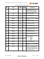
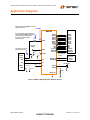
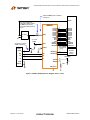
USB3310 Hi-Speed USB Transceiver with 1.8V ULPI Interface Multi-Frequency Reference Clock PRODUCT FEATURES Data Brief USB-IF “Hi-Speed” compliant to the Universal Serial Bus Specification Rev 2.0 Interface compliant with the ULPI Specification revision 1.1 as a Single Data Rate (SDR) PHY 1.8V IO Voltage (±10%) flexPWRTM Technology — Low current design ideal for battery powered applications — “Sleep” mode tri-states all ULPI pins and places the part in a low current state Supports FS pre-amble for FS hubs with a LS device attached (UTMI+ Level 3) Supports HS SOF and LS keep-alive pulse Includes full support for the optional On-The-Go (OTG) protocol detailed in the On-The-Go Supplement Revision 1.0a specification Supports the OTG Host Negotiation Protocol (HNP) and Session Request Protocol (SRP) Allows host to turn VBUS off to conserve battery power in OTG applications Support OTG monitoring of VBUS levels with internal comparators “Wrapper-less” design for optimal timing performance and design ease — Low Latency Hi-Speed Receiver (43 Hi-Speed clocks Max) allows use of legacy UTMI Links with a ULPI bridge Internal 5V cable short-circuit protection of ID, DP and DM lines to VBUS or ground 13, 19.2, 24 or 26MHz Selectable Reference ClockFrequency Integrated ESD protection circuits — Up to ±15kV without any external devices Carkit UART mode for non-USB serial data transfers Industrial Operating Temperature -40°C to +85°C Packaging Options — 24 pin QFN lead-free RoHS compliant package (4 x 4 x 0.90 mm height) Applications The USB3310 is targeted for any application where a HiSpeed USB connection is desired and when board space, power, and interface pins must be minimized. The USB3310 is well suited for: Cell Phones PDAs MP3 Players GPS Personal Navigation Scanners External Hard Drives Digital Still and Video Cameras Portable Media Players Entertainment Devices Printers Set Top Boxes Video Record/Playback Systems IP and Video Phones Gaming Consoles POS Terminals — 0 to 3.6V input drive tolerant — Able to accept “noisy” clock sources Internal low jitter PLL for 480MHz Hi-Speed USB operation Internal detection of the value of resistance to ground on the ID pin Integrated battery to 3.3V LDO regulator — 2.2uF bypass capacitor — 100mV dropout voltage SMSC USB3310 REV C PRODUCT PREVIEW Revision 1.11 (10-31-08) Hi-Speed USB Transceiver with 1.8V ULPI Interface - Multi-Frequency Reference Clock Order Number(s): USB3310C-CP-TR FOR 24 PIN, QFN LEAD-FREE ROHS COMPLIANT PACKAGE (TAPE AND REEL) REEL SIZE IS 4000 PIECES. 80 ARKAY DRIVE, HAUPPAUGE, NY 11788 (631) 435-6000, FAX (631) 273-3123 Copyright © 2008 SMSC or its subsidiaries. All rights reserved. Circuit diagrams and other information relating to SMSC products are included as a means of illustrating typical applications. Consequently, complete information sufficient for construction purposes is not necessarily given. Although the information has been checked and is believed to be accurate, no responsibility is assumed for inaccuracies. SMSC reserves the right to make changes to specifications and product descriptions at any time without notice. Contact your local SMSC sales office to obtain the latest specifications before placing your product order. The provision of this information does not convey to the purchaser of the described semiconductor devices any licenses under any patent rights or other intellectual property rights of SMSC or others. All sales are expressly conditional on your agreement to the terms and conditions of the most recently dated version of SMSC's standard Terms of Sale Agreement dated before the date of your order (the "Terms of Sale Agreement"). The product may contain design defects or errors known as anomalies which may cause the product's functions to deviate from published specifications. Anomaly sheets are available upon request. SMSC products are not designed, intended, authorized or warranted for use in any life support or other application where product failure could cause or contribute to personal injury or severe property damage. Any and all such uses without prior written approval of an Officer of SMSC and further testing and/or modification will be fully at the risk of the customer. Copies of this document or other SMSC literature, as well as the Terms of Sale Agreement, may be obtained by visiting SMSC’s website at http://www.smsc.com. SMSC is a registered trademark of Standard Microsystems Corporation (“SMSC”). Product names and company names are the trademarks of their respective holders. SMSC DISCLAIMS AND EXCLUDES ANY AND ALL WARRANTIES, INCLUDING WITHOUT LIMITATION ANY AND ALL IMPLIED WARRANTIES OF MERCHANTABILITY, FITNESS FOR A PARTICULAR PURPOSE, TITLE, AND AGAINST INFRINGEMENT AND THE LIKE, AND ANY AND ALL WARRANTIES ARISING FROM ANY COURSE OF DEALING OR USAGE OF TRADE. IN NO EVENT SHALL SMSC BE LIABLE FOR ANY DIRECT, INCIDENTAL, INDIRECT, SPECIAL, PUNITIVE, OR CONSEQUENTIAL DAMAGES; OR FOR LOST DATA, PROFITS, SAVINGS OR REVENUES OF ANY KIND; REGARDLESS OF THE FORM OF ACTION, WHETHER BASED ON CONTRACT; TORT; NEGLIGENCE OF SMSC OR OTHERS; STRICT LIABILITY; BREACH OF WARRANTY; OR OTHERWISE; WHETHER OR NOT ANY REMEDY OF BUYER IS HELD TO HAVE FAILED OF ITS ESSENTIAL PURPOSE, AND WHETHER OR NOT SMSC HAS BEEN ADVISED OF THE POSSIBILITY OF SUCH DAMAGES. Revision 1.11 (10-31-08) 2 PRODUCT PREVIEW SMSC USB3310 REV C Hi-Speed USB Transceiver with 1.8V ULPI Interface - Multi-Frequency Reference Clock General Description The USB3310 is a highly integrated Hi-Speed USB 2.0 Transceiver (PHY) that supports systems architectures based on a 13, 19.2, 24 or 26MHz reference clock. The frequency of the reference clock is selected by configuration. It is designed to be used in both commercial and industrial temperature applications. The USB3310 meets all of the electrical requirements to be used as a Hi-Speed USB Host, Device, or an On-the-Go (OTG) device. In addition to the supporting USB signaling the USB3310 also provides USB UART mode. USB3310 uses the industry standard UTMI+ Low Pin Interface (ULPI) to connect the USB PHY to the Link. The industry standard ULPI interface uses a method of in-band signaling and status byte transfers between the Link and PHY, to facilitate a USB session. By using in-band signaling and status byte transfers the ULPI interface requires only 12 pins. The USB3310 uses SMSC’s “wrapper-less” technology to implement the ULPI interface. This “wrapperless” technology allows the PHY to achieve a low latency transmit and receive time. SMSC’s low latency transceiver allows an existing UTMI Link to be reused by adding a UTMI to ULPI bridge. By adding a bridge to the ASIC the existing and proven UTMI Link IP can be reused. REFSEL[1] REFSEL[0] ID DP DM ESD Protection VBUS OTG Hi-Speed USB Transceiver REFCLK Low Jitter Integrated PLL ULPI Registers and State Machine BIAS RBIAS Integrated Power Management RESETB VBAT VDD33 VDD18 ULPI Interface STP NXT DIR CLKOUT Carkit DATA[7:0] Figure 1 USB3310 Block Diagram The USB3310 is designed to operate with an external reference clock at one of four frequencies. By using an available reference, the USB3310 saves the cost of a crystal reference. The USB3310 includes a integrated 3.3V LDO regulator to generate its own supply from power applied at the VBAT pin. The voltage on the VBAT pin can range from 3.1 to 5.5V. The regulator dropout voltage is less than 100mV which allows the PHY to continue USB signaling when the voltage on VBAT drops to 3.1V. The USB transceiver will continue to operate at lower voltages, although some parameters may be outside the limits of the USB specifications. If the user would like to provide a 3.3V supply to the USB3310, the VBAT and VDD33 pins should be connected together. The USB3310 also includes integrated pull-up resistors that can be used for detecting the attachment of a USB Charger. By sensing the attachment to a USB Charger, a product using the USB3310 can charge its battery at more than the 500mA allowed when charging from a USB Host. SMSC USB3310 REV C 3 PRODUCT PREVIEW Revision 1.11 (10-31-08) Hi-Speed USB Transceiver with 1.8V ULPI Interface - Multi-Frequency Reference Clock USB3310 Pin Locations and Descriptions Package Diagram with Pin Locations RBIAS REFCLK RESETB VDD1.8 STP DIR 24 23 22 21 20 19 The pinout below is viewed from the top of the package. ID 1 18 NXT VBUS 2 17 DATA0 VBAT 3 16 DATA1 VDD3.3 4 15 REFSEL[0] DM 5 14 REFSEL[1] DP 6 13 DATA2 8 9 10 11 12 DATA6 DATA5 DATA4 CLKOUT DATA3 DATA7 7 24Pin QFN 4x4mm Figure 2 USB3310 QFN Pinout - Top View Pin Definitions The following table details the pin definitions for the figure above. Table 1 USB3310 Pin Description PIN BALL NAME DIRECTION/ TYPE ACTIVE LEVEL DESCRIPTION 1 B1 ID Input, Analog N/A ID pin of the USB cable. For non-OTG applications this pin can be floated. For an A-Device ID is grounded. For a BDevice ID is floated. 2 C1 VBUS I/O, Analog N/A VBUS pin of the USB cable. This pin is used for the Vbus comparator inputs and for Vbus pulsing during session request protocol. 3 C2 VBAT Power N/A Regulator input. The regulator supply can be from 5.5V to 3.1V. Revision 1.11 (10-31-08) 4 PRODUCT PREVIEW SMSC USB3310 REV C Hi-Speed USB Transceiver with 1.8V ULPI Interface - Multi-Frequency Reference Clock Table 1 USB3310 Pin Description (continued) PIN BALL NAME DIRECTION/ TYPE ACTIVE LEVEL 4 D2 VDD3.3 Power N/A 3.3V Regulator Output. A 2.2uF (<1 ohm ESR) bypass capacitor to ground is required for regulator stability. The bypass capacitor should be placed as close as possible to the USB3310. 5 D1 DM I/O, Analog N/A D- pin of the USB cable. 6 E1 DP I/O, Analog N/A D+ pin of the USB cable. 7 E2 DATA[7] I/O, CMOS N/A ULPI bi-directional data bus. DATA[7] is the MSB. 8 E3 DATA[6] I/O, CMOS N/A ULPI bi-directional data bus. 9 D3 DATA[5 I/O, CMOS N/A ULPI bi-directional data bus. 10 E4 DATA[4] I/O, CMOS N/A ULPI bi-directional data bus. 11 E5 CLKOUT Output, CMOS N/A 60MHz reference clock output. All ULPI signals are driven synchronous to the rising edge of this clock. 12 D5 DATA[3] I/O, CMOS N/A ULPI bi-directional data bus. 13 D4 DATA[2] I/O, CMOS N/A ULPI bi-directional data bus. 14 C4 REFSEL[1] Input, CMOS N/A 15 B4 REFSEL[0] Input, CMOS N/A These signals select one of the available reference frequencies: [1] [0] Description 0 0 13MHz 0 1 19.2MHz 1 0 26MHz 1 1 24MHz 16 C5 DATA[1] I/O, CMOS N/A ULPI bi-directional data bus. 17 B5 DATA[0] I/O, CMOS N/A ULPI bi-directional data bus. DATA[0] is the LSB. 18 A5 NXT Output, CMOS High The PHY asserts NXT to throttle the data. When the Link is sending data to the PHY, NXT indicates when the current byte has been accepted by the PHY. The Link places the next byte on the data bus in the following clock cycle. SMSC USB3310 REV C 5 PRODUCT PREVIEW DESCRIPTION Revision 1.11 (10-31-08) Hi-Speed USB Transceiver with 1.8V ULPI Interface - Multi-Frequency Reference Clock Table 1 USB3310 Pin Description (continued) PIN BALL NAME DIRECTION/ TYPE ACTIVE LEVEL DESCRIPTION 19 A4 DIR Output, CMOS N/A Controls the direction of the data bus. When the PHY has data to transfer to the Link, it drives DIR high to take ownership of the bus. When the PHY has no data to transfer it drives DIR low and monitors the bus for commands from the Link. 20 A3 STP Input, CMOS High The Link asserts STP for one clock cycle to stop the data stream currently on the bus. If the Link is sending data to the PHY, STP indicates the last byte of data was on the bus in the previous cycle. 21 B3 VDD1.8 Power N/A External 1.8V Supply input pin. This pad needs to be bypassed with a 0.1uF capacitor to ground, placed as close as possible to the USB3310. 22 B2 RESETB Input, CMOS, N/A When low, the part is suspended with all of the I/O tri-stated. When high the USB3310 will operate as a normal ULPI device. 23 A2 REFCLK Input, CMOS N/A Reference Clock input.The required frequency is configured by the REFSEL[1:0] pins. 24 A1 RBIAS Analog, CMOS N/A Rbias pin. This pin requires an 8.06kΩ (±1%) resistor to ground, placed as close as possible to the USB3310. FLAG C3 GND Ground N/A Ground. QFN only: The flag should be connected to the ground plane with a via array under the exposed flag. This is the main ground for the IC. Revision 1.11 (10-31-08) 6 PRODUCT PREVIEW SMSC USB3310 REV C Hi-Speed USB Transceiver with 1.8V ULPI Interface - Multi-Frequency Reference Clock Application Diagrams Steady state voltage at the VBUS pin must not be allowed to exceed VVMAX. Link Controller USB331X RVBUS may be installed in this configuration to assist in protecting the VBUS pin. 820 Ohms will protect against VBUS transients up to 8.5V. 10K Ohms will protect against transients up to 10V. RVBUS 2 VBUS 3 VBAT 4 VDD3.3 3.1-5.5V Supply The capacitor CVBUS must be installed on this side of RVBUS. CBYP USB Receptacle CVBUS COUT VBUS 1 DM 2 5 DM DP 3 6 DP NC SHIELD GND DATA7 DATA6 DATA5 DATA4 DATA3 DATA2 DATA1 DATA0 STP NXT DIR CLKOUT RESETB REFCLK 1 7 8 9 10 12 13 16 17 20 18 19 11 22 23 DATA7 DATA6 DATA5 DATA4 DATA3 DATA2 DATA1 DATA0 STP NXT DIR CLKOUT RESETB Reference Signal at REFCLK must comply with VIH and VIL 14 REFSEL[1] REFSEL[0] 15 VDD18 21 RBIAS 24 Pin Strap Determines REFCLK frequency 1.8V Supply ID CDC_BLOCK CBYP 8.06k GND FLAG Figure 3 USB3310 QFN Application Diagram (Device) SMSC USB3310 REV C 7 PRODUCT PREVIEW Revision 1.11 (10-31-08) Hi-Speed USB Transceiver with 1.8V ULPI Interface - Multi-Frequency Reference Clock Voltage at the VBUS pin must not be allowed to exceed VVMAX. Link Controller CPEN RVBUS may be installed in this configuration to assist in protecting the VBUS pin. 820 Ohms will protect against VBUS transients up to 8.5V. USB331X VBUS Switch RVBUS EN OUT IN 2 VBUS 3 VBAT 4 VDD3.3 5V 3.1 - 5.5V Supply The capacitor CVBUS must be installed on this side of RVBUS. USB Receptacle CBYP CVBUS DATA7 DATA6 DATA5 DATA4 DATA3 DATA2 DATA1 DATA0 STP NXT DIR CLKOUT RESETB REFCLK COUT VBUS 1 DM 2 5 DM DP 3 6 DP ID 4 1 ID REFSEL[1] REFSEL[0] 7 8 9 10 12 13 16 17 20 18 19 11 22 23 DATA7 DATA6 DATA5 DATA4 DATA3 DATA2 DATA1 DATA0 STP NXT DIR CLKOUT RESETB Reference Signal at REFCLK must comply with VIH and VIL 14 15 Pin Strap Determines REFCLK frequency 1.8V Supply VDD18 RBIAS GND SHIELD 21 24 CBYP 8.06k GND FLAG Figure 4 USB3310 QFN Application Diagram (Host or OTG) Revision 1.11 (10-31-08) 8 PRODUCT PREVIEW SMSC USB3310 REV C PRODUCT PREVIEW 9 Hi-Speed USB Transceiver with 1.8V ULPI Interface - Multi-Frequency Reference Clock Revision 1.11 (10-31-08) Package Outline SMSC USB3310 REV C Figure 5 24-Pin QFN, 4x4mm Body, 0.5mm Pitch