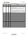
1
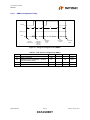
USB20H04 4-Port USB 2.0 Hub Controller Datasheet Product Features General Features Compliant with USB 2.0 Specification OEM Selectable Features Configure as a bus-powered or self-powered Hi-Speed USB hub Four transaction translators ensure maximum USB throughput Configure port power switching and current sensing on an individual or ganged basis Enables bus-powered Hi-Speed hub design Enable LED indicator support Compatible with On-The-Go (OTG) USB devices Enable multiple transaction translators Integrated Session Request Protocol (SRP) operates with dual-role OTG hosts Enable compound device support on a port by port basis Default configuration with pin selectable options Serial interface for configuration from EEPROM or microcontroller when default is not used Enable downstream facing ports on a port by port basis Flexible OEM configuration options Pin Selectable Options for Default Configuration Available in a 64-pin TQFP package Hub controller IC with four downstream ports Select operation as either a Bus-Powered hub or a Self-Powered hub Hardware Features Detects removal of self-power and automatically changes mode to bus-power Integrated termination and pull-up/pull-down resistors Internal short circuit protection of DP and DM lines On-chip oscillator uses low cost 24MHz crystal Supports individual or ganged over-current protection and power control LED drivers for each downstream port ORDERING INFORMATION Order Number(s): USB20H04-JD for 64 pin, 10x10x1.4 TQFP package USB20H04-JT for 64 pin, 10x10x1.4 TQFP Lead-Free RoHS Compliant Package SMSC USB20H04 Page 1 DATASHEET Revision 1.63 (03-30-07) 4-Port USB 2.0 Hub Controller Datasheet 80 ARKAY DRIVE, HAUPPAUGE, NY 11788 (631) 435-6000, FAX (631) 273-3123 Copyright © 2007 SMSC or its subsidiaries. All rights reserved. Circuit diagrams and other information relating to SMSC products are included as a means of illustrating typical applications. Consequently, complete information sufficient for construction purposes is not necessarily given. Although the information has been checked and is believed to be accurate, no responsibility is assumed for inaccuracies. SMSC reserves the right to make changes to specifications and product descriptions at any time without notice. Contact your local SMSC sales office to obtain the latest specifications before placing your product order. The provision of this information does not convey to the purchaser of the described semiconductor devices any licenses under any patent rights or other intellectual property rights of SMSC or others. All sales are expressly conditional on your agreement to the terms and conditions of the most recently dated version of SMSC's standard Terms of Sale Agreement dated before the date of your order (the "Terms of Sale Agreement"). The product may contain design defects or errors known as anomalies which may cause the product's functions to deviate from published specifications. Anomaly sheets are available upon request. SMSC products are not designed, intended, authorized or warranted for use in any life support or other application where product failure could cause or contribute to personal injury or severe property damage. Any and all such uses without prior written approval of an Officer of SMSC and further testing and/or modification will be fully at the risk of the customer. Copies of this document or other SMSC literature, as well as the Terms of Sale Agreement, may be obtained by visiting SMSC’s website at http://www.smsc.com. SMSC is a registered trademark of Standard Microsystems Corporation (“SMSC”). Product names and company names are the trademarks of their respective holders. SMSC DISCLAIMS AND EXCLUDES ANY AND ALL WARRANTIES, INCLUDING WITHOUT LIMITATION ANY AND ALL IMPLIED WARRANTIES OF MERCHANTABILITY, FITNESS FOR A PARTICULAR PURPOSE, TITLE, AND AGAINST INFRINGEMENT AND THE LIKE, AND ANY AND ALL WARRANTIES ARISING FROM ANY COURSE OF DEALING OR USAGE OF TRADE. IN NO EVENT SHALL SMSC BE LIABLE FOR ANY DIRECT, INCIDENTAL, INDIRECT, SPECIAL, PUNITIVE, OR CONSEQUENTIAL DAMAGES; OR FOR LOST DATA, PROFITS, SAVINGS OR REVENUES OF ANY KIND; REGARDLESS OF THE FORM OF ACTION, WHETHER BASED ON CONTRACT; TORT; NEGLIGENCE OF SMSC OR OTHERS; STRICT LIABILITY; BREACH OF WARRANTY; OR OTHERWISE; WHETHER OR NOT ANY REMEDY OF BUYER IS HELD TO HAVE FAILED OF ITS ESSENTIAL PURPOSE, AND WHETHER OR NOT SMSC HAS BEEN ADVISED OF THE POSSIBILITY OF SUCH DAMAGES. Revision 1.63 (03-30-07) Page 2 DATASHEET SMSC USB20H04 4-Port USB 2.0 Controller Datasheet Table of Contents Chapter 1 1.1 1.2 1.3 General Description ............................................................................................................. 5 Applications ......................................................................................................................................... 5 OEM Selectable Features ................................................................................................................... 6 Pin Selectable Options to the Default Configuration........................................................................... 6 Chapter 2 Functional Block Diagram .................................................................................................. 7 Chapter 3 Pinout .................................................................................................................................... 8 Chapter 4 Interface Signal Definition .................................................................................................. 9 4.1 4.2 Pin Descriptions .................................................................................................................................. 9 Buffer Type Descriptions ................................................................................................................... 11 Chapter 5 Limiting Values .................................................................................................................. 12 Chapter 6 Electrical Characteristics .................................................................................................. 13 6.1 Dynamic Characteristics: Analog I/O Pins (DP/DM) ......................................................................... 15 Chapter 7 7.1 7.2 7.3 7.4 7.5 Functional Overview.......................................................................................................... 16 Bus-Power Detect ............................................................................................................................. 16 Upstream PHY .................................................................................................................................. 16 Clock/PLL .......................................................................................................................................... 16 Internal Configuration Select............................................................................................................. 16 Serial Interface .................................................................................................................................. 17 7.5.1 7.5.2 7.6 7.7 7.8 7.9 7.10 7.11 7.12 SMBus Slave ..........................................................................................................................................17 I2C Memory Interface ..............................................................................................................................17 Repeater............................................................................................................................................ 17 SIE..................................................................................................................................................... 17 Controller ........................................................................................................................................... 17 Transaction Translator (TT) .............................................................................................................. 18 Port Controller ................................................................................................................................ 18 Downstream PHY........................................................................................................................... 18 OC Sense/Switch Driver ................................................................................................................ 18 7.12.1 7.12.2 7.13 Over-Current Sense ............................................................................................................................18 Switch Driver .......................................................................................................................................18 LED Drivers.................................................................................................................................... 18 Chapter 8 8.1 8.1.1 8.1.2 8.2 8.3 8.4 Implementation Notes........................................................................................................ 20 Configuration Implementations ......................................................................................................... 20 Interfacing a 2-wire Serial EEPROM.......................................................................................................20 Internal Default Configuration .................................................................................................................21 EEPROM Programming Values ........................................................................................................ 21 Default Configuration Values ............................................................................................................ 23 Reset ................................................................................................................................................. 24 8.4.1 8.4.2 External Hardware Reset........................................................................................................................24 USB Reset ..............................................................................................................................................27 Chapter 9 Hub Descriptors ................................................................................................................. 28 Chapter 10 Application Diagrams..................................................................................................... 33 Chapter 11 Package Outline .............................................................................................................. 35 SMSC USB20H04 Page 3 DATASHEET Revision 1.63 (03-30-07) 4-Port USB 2.0 Hub Controller Datasheet List of Figures Figure 2.1 - Block Diagram.............................................................................................................................................7 Figure 3.1– 64 Pin TQFP ...............................................................................................................................................8 Figure 8.1 - 2-Wire EEPROM Interface........................................................................................................................20 Figure 8.2 - Internal Default Mode................................................................................................................................21 Figure 8.3 - Timing for Configuration from SMBus .......................................................................................................25 Figure 8.4 - Timing to Complete Configuration from EEPROM ....................................................................................26 Figure 10.1 - High Level Block Diagram of a Self-Powered Hub ..................................................................................33 Figure 10.2 - USB Downstream Port Connection .........................................................................................................34 Figure 11.1 - 64 Pin TQFP Package Outline, 10 x 10 x 1.4 Body, 2 MM Footprint ......................................................35 List of Tables Table 4.1 - System Interface Signals .............................................................................................................................9 Table 4.2 – Configuration Select and Serial Port Interface.............................................................................................9 Table 4.3 - USB I/O Signals .........................................................................................................................................10 Table 4.4 - Biasing and Clock Oscillator Signals..........................................................................................................11 Table 4.5 - Power and Ground Signals ........................................................................................................................11 Table 4.6 – USB20H04 Buffer Type Descriptions ........................................................................................................11 Table 5.1 - Absolute Maximum Ratings (In accordance with the Absolute Maximum Rating system (IEC 60134).......12 Table 5.2 - Recommended Operating Conditions ........................................................................................................12 Table 5.3 - Recommended Crystal/External Clock Conditions .....................................................................................12 Table 6.1 - Electrical Characteristics: Supply Pins .......................................................................................................13 Table 6.2 - DC Electrical Characteristics: Digital Pins ..................................................................................................13 Table 6.3 - Pin Capacitance .........................................................................................................................................14 Table 6.4 - DC Electrical Characteristics: Analog I/O Pins (DP/DM) ............................................................................15 Table 7.1 - Automatic Mode Port Indicators .................................................................................................................19 Table 7.2 - Manual Mode Port Indicators .....................................................................................................................19 Table 8.1 - Summary of OEM Value Programming ......................................................................................................21 Table 8.2 - Address 6; Config_Byte_3..........................................................................................................................22 Table 8.3 - Address 7; Config_Byte_2..........................................................................................................................22 Table 8.4 - Address 8; Config_Byte_1..........................................................................................................................23 Table 8.5 - Addresses 9 - 11 ........................................................................................................................................23 Table 8.6 - Default Configuration Values......................................................................................................................24 Table 8.7 - Time Values to Configure from SMBus ......................................................................................................25 Table 8.8 - Time Values to Configure From EEPROM.................................................................................................26 Table 9.1 - Device Descriptor.......................................................................................................................................28 Table 9.2 - Device Qualifier Descriptor ........................................................................................................................28 Table 9.3 - Standard Configuration Descriptor .............................................................................................................29 Table 9.4 - Other_Speed_Configuration Descriptor .....................................................................................................29 Table 9.5 - Standard Interface Descriptor ....................................................................................................................30 Table 9.6 - Standard Endpoint Descriptor ....................................................................................................................30 Table 9.7 - Interface Descriptor (present if multiple-TT)...............................................................................................31 Table 9.8 - On-The-GO (OTG) Descriptor....................................................................................................................31 Table 9.9 - Class-Specific Hub Descriptor (Full-Speed and High-Speed) ....................................................................31 Table 11.1 - 64 Pin TQFP Package Parameters ..........................................................................................................35 Revision 1.63 (03-30-07) Page 4 DATASHEET SMSC USB20H04 4-Port USB 2.0 Controller Datasheet Chapter 1 General Description The USB20H04 four-port hub controller is fully compliant with the USB 2.0 Specification and does not require firmware development. When connected to a high-speed host, the four downstream facing ports can operate at low-speed (1.5Mb/s), full-speed (12Mb/s), or high-speed (480Mb/s). As required by the USB 2.0 Specification, the USB20H04 is fully backward compatible with legacy full-speed hosts. A dedicated Transaction Translator (TT) is available for each downstream facing port. This architecture ensures maximum USB throughput for each connected device when operating with mixed-speed peripherals. The USB20H04 supports both bus-powered and self-powered configurations. For self-powered operation, an external supply is used to power the downstream facing ports. In bus-powered mode, all power is derived from the upstream facing port and no external power supply is required. An external USB power distribution switch device is used to control VBUS switching to downstream ports, and to limit current and sense over-current conditions. A default configuration is available in the USB20H04 following a reset. This configuration may be sufficient for some applications when it is desired to save the expense of an EEPROM. The controller may also be configured from a microcontroller or an external EEPROM. When using the microcontroller interface, the USB20H04 appears as an SMBus slave device. The EEPROM interface supports a 2-wire I2C device. All required resistors on the USB ports are integrated into the USB20H04. This includes all series termination resistors on D+ and D– pins and all required pull-down and pull-up resistors on D+ and D– pins. The over-current sense inputs for the downstream facing ports have internal pull-up resistors. Throughout this document the upstream facing port of the hub will be referred to as the upstream port, and the four downstream facing ports will be called the downstream ports. 1.1 Applications The Universal Serial Bus (USB) hub may be used in a number of applications: SMSC USB20H04 Standalone hubs Keyboards Monitors Motherboard hubs Docking stations and port replicators Printers and scanners External storage devices Auxiliary battery docks Page 5 DATASHEET Revision 1.63 (03-30-07) 4-Port USB 2.0 Hub Controller Datasheet 1.2 OEM Selectable Features The 4-Port Hub supports several OEM selectable features: 1.3 Operation as a bus-powered, self-powered or dynamic-powered hub. (When configured for dynamic operation, the controller automatically switches to bus-powered mode if a local power source is unavailable). Configure downstream facing port power switching on an individual or ganged basis. Configure downstream facing port over-current sensing on an individual or ganged basis. Enable downstream facing port LED indicators. Select multiple or single transaction translator mode. Select whether the hub is part of a compound device (when any downstream facing port is permanently hardwired to a USB peripheral device, the hub is part of a compound device). Select the presence of a permanently hardwired USB peripheral device on a port by port basis. Enable downstream facing ports a port by port basis. Enable EOP generation of EOF1 when operating in full-speed mode, as described in Section 11.3.1 of the USB 2.0 Specification. Enable USB On-The-Go Session Request Protocol (SRP) support. Configure the delay time for filtering the over-current sense inputs. Configure the delay time until port power is good after the SetPortPower command is received. Indicate the maximum current that the 4-port hub consumes from an upstream port. Indicate the maximum current required for the hub controller. Pin Selectable Options to the Default Configuration The USB20H04 includes a default configuration for those applications where an external EEPROM or SMBus device is not available to provide the configuration. This configuration may be adequate in some applications. A pin selectable feature supports configuration as either a bus-powered hub or a self-powered hub determined by the logic level of the SELF_PWR pin following reset. Revision 1.63 (03-30-07) Page 6 DATASHEET SMSC USB20H04 4-Port USB 2.0 Controller Datasheet Chapter 2 Functional Block Diagram To Upstream VBUS Upstream USB Data Pin Selectable Options 24 MHz Crystal To EEPROM or SMBus Master SD SCK Bus-Power Detect/ VBUS Pulse Internal Configuration Select PLL Upstream PHY SIE Repeater TT #1 TT #2 TT #3 Serial Interface Controller TT #4 Port Controller Routing Logic Port #1 Downstream OC Sense PHY #1 Switch Driver LED Drivers Port #4 Downstream OC Sense PHY #4 Switch Driver LED Drivers Downstream OC Switch/LED USB Data Sense Drivers Downstream OC Switch/LED USB Data Sense Drivers Figure 2.1 - Block Diagram SMSC USB20H04 Page 7 DATASHEET Revision 1.63 (03-30-07) 4-Port USB 2.0 Hub Controller Datasheet XTAL2 VDDA18 VSS VDD18 VSS VBUSDET SELF_PWR SMB_SEL_N RESET_N 56 55 54 53 52 51 50 49 XTAL1/CLKIN VSS 59 58 57 VDDA18 60 ATEST 62 VDDA33 RBIAS 63 61 VSS Pinout 64 Chapter 3 VDDA33 1 48 TEST_P3 USBDP0 2 47 CLKIN_EN USBDM0 46 OCS1_N VSS 3 4 45 VBUS1_N USBDM1 5 44 OCS2_N USBDP1 6 43 VBUS2_N VDDA33 7 42 USBDP2 8 41 VDD18 VSS USBDM2 9 40 OCS3_N USB20H04 25 26 27 28 29 30 31 32 AM1_N GR1_N VDD33 VSS VDD18 TEST_P0 TEST_P1 33 GR2_N SD/SDA TEST_P2 AM2_N 34 16 23 24 15 VSS VSS USBDM4 22 SCK/SCL 21 35 AM3_N 14 GR3_N CS/EESEL USBDP4 20 VBUS4_N 36 GR4_N 37 13 19 12 VDDA33 AM4_N OCS4_N USBDP3 18 VBUS3_N 38 NC 39 11 17 10 NC VSS USBDM3 Figure 3.1– 64 Pin TQFP Revision 1.63 (03-30-07) Page 8 DATASHEET SMSC USB20H04 4-Port USB 2.0 Controller Datasheet Chapter 4 4.1 Interface Signal Definition Pin Descriptions Table 4.1 - System Interface Signals RESET_N BUFFER TYPE IS SELF_PWR I TEST_P0 TEST_P1 TEST_P2 TEST_P3 ATEST IPD IPD IPD IPD AO NAME ACTIVE DESCRIPTION LEVEL Low Chip Reset. The minimum active low pulse is 100ns. See section 8.4 for a complete description of operation following a reset. Self-power Detect. Detects availability of local self-power source: High 0: Self/local power source is NOT available (i.e., 4- Port Hub gets all power from Upstream USB VBUS). 1: Self/local power source is available. N/A N/A N/A N/A N/A Test Pin. Do Not Connect Test Pin. Do Not Connect Test Pin. Do Not Connect Test Pin. Do Not Connect Test Pin. Do Not Connect Table 4.2 – Configuration Select and Serial Port Interface NAME BUFFER TYPE SMB_SEL_N I ACTIVE LEVEL N/A CS/EE_SEL IO8 N/A SD/SDA SCK/SCL IOSD12 IOSD12 N/A N/A SMSC USB20H04 DESCRIPTION SMBus Select. Selects between configuration via the SMBus interface, or from an external EEPROM or using the internal default, as described in the table below. SMB_SEL_N CS/EE_SEL SMBus or EEPROM interface configuration. 0 0 SMBus slave. Address: 0101100 0 1 SMBus slave. Address: 0101101 1 0 Internal default configuration. 1 1 2-wire EEPROM interface. Chip Select. This multifunction pin is sampled on the rising edge of RESET_N. If SMB_SEL_N = 1, the internal default configuration will be used when this pin is low, or the external I2C EEPROM will supply the configuration when this pin is high. When SMB_SEL_N = 0, this pin selects the SMBus slave address, as described in the table above. Connect a 1k ohm resistor in series with the input when connecting this pin to either VDD or VSS. Serial Data. Data I/O on the 2-Wire interface. Serial Clock. Clock for the 2-Wire interface. Page 9 DATASHEET Revision 1.63 (03-30-07) 4-Port USB 2.0 Hub Controller Datasheet Table 4.3 - USB I/O Signals NAME USBDP0 USBDM0 VBUSDET BUFFER TYPE IO-U IO-U IO8 ACTIVE DESCRIPTION LEVEL N/A Upstream USB Positive Data Pin. N/A Upstream USB Negative Data Pin. N/A Detects state of upstream VBUS power. When designing a detachable hub, this pin must be connected to the VBUS power pin of the USB port that is upstream of the hub. For self-powered applications with a permanently attached upstream host, this pin must be connected to either 3.3V or 5.0V (typically VDD3.3). The USB20H04 monitors VBUSDET to determine when to assert the internal D+ pull-up resistor (signaling a connect event). When using the SRP feature, it is necessary to add a 100k ohm resistor from this pin to VSS in order to properly dissipate the upstream VBUS Pulse (pulsed with an 8mA drive capability). USBDP1 USBDM1 VBUS1_N OCS1_N GR1_N AM1_N USBDP2 USBDM2 VBUS2_N OCS2_N GR2_N AM2_N USBDP3 USBDM3 VBUS3_N OCS3_N GR3_N AM3_N USBDP4 USBDM4 VBUS4_N OCS4_N GR4_N AM4_N Revision 1.63 (03-30-07) IO-U IO-U O8 IPU OD8 OD8 IO-U IO-U O8 IPU OD8 OD8 IO-U IO-U O8 IPU OD8 OD8 IO-U IO-U O8 IPU OD8 OD8 N/A N/A Low Low Low Low N/A N/A Low Low Low Low N/A N/A Low Low Low Low N/A N/A Low Low Low Low USB Positive Data Pin to downstream port 1. USB Negative Data Pin to downstream port 1. Enables power to downstream port 1. Over-Current Sense input. Internal pull-up resistor to 3.3V. Enables green indicator to downstream port 1. Enables amber indicator to downstream port 1. USB Positive Data Pin to downstream port 2. USB Negative Data Pin to downstream port 2. Enables power to downstream port 2. Over-Current Sense input. Internal pull-up resistor to 3.3V. Enables green indicator to downstream port 2. Enables amber indicator to downstream port 2. USB Positive Data Pin to downstream port 3. USB Negative Data Pin to downstream port 3. Enables power to downstream port 3. Over-Current Sense input. Internal pull-up resistor to 3.3V. Enables green indicator to downstream port 3. Enables amber indicator to downstream port 3. USB Positive Data Pin to downstream port 4. USB Negative Data Pin to downstream port 4. Enables power to downstream port 4. Over-Current Sense input. Internal pull-up resistor to 3.3V. Enables green indicator to downstream port 4. Enables amber indicator to downstream port 4. Page 10 DATASHEET SMSC USB20H04 4-Port USB 2.0 Controller Datasheet Table 4.4 - Biasing and Clock Oscillator Signals RBIAS BUFFER TYPE I-R XTAL1/CLKIN ICLKx XTAL2 OCLKx N/A External crystal. 24MHz crystal. Not connected when using an external clock. CLKIN_EN I High Clock Input Enable. When high, an external CMOS clock drives XTAL1. NAME ACTIVE DESCRIPTION LEVEL N/A External 1% bias resistor. Requires a 12KΩ resistor to ground. Used for setting HS transmit current level and on-chip termination impedance. N/A External crystal. 24MHz crystal or external clock input when a crystal is not used. Connect a 5M ohm resistor from this pin to XTAL2 when a crystal is used. Table 4.5 - Power and Ground Signals NAME BUFFER TYPE ACTIVE LEVEL VDD3.3 N/A N/A DESCRIPTION 3.3V Digital Supply. Powers digital pads. VDD1.8 N/A N/A 1.8V Digital Supply. Powers digital core. VSS VDDA3.3 N/A N/A N/A N/A Signal Ground. 3.3V Analog Supply. Powers analog I/O and 3.3V analog circuitry. VDDA1.8 N/A N/A 1.8V Analog Supply. Powers 1.8V analog circuitry. 4.2 Buffer Type Descriptions Table 4.6 – USB20H04 Buffer Type Descriptions BUFFER I IPU IPD IS IO8 IOSD12 O8 OD8 ICLKx OCLKx IO-U AO I-R SMSC USB20H04 DESCRIPTION Input Input with weak internal pull-up resistor. Input with weak internal pull-down resistor Input with Schmitt trigger Input/Output with 8mA drive Open drain with 12mA sink with Schmitt trigger. Meets I2C-Bus Spec Version 2.1 Output with 8mA drive Open drain with 8mA sink XTAL clock input XTAL clock output Defined in USB specification Analog Output 3.3V Tolerant Analog Pin Page 11 DATASHEET Revision 1.63 (03-30-07) 4-Port USB 2.0 Hub Controller Datasheet Chapter 5 Limiting Values Table 5.1 - Absolute Maximum Ratings (In accordance with the Absolute Maximum Rating system (IEC 60134) PARAMETER 1.8V Supply Voltage (VDD1.8 and VDDA1.8) 3.3V Supply Voltage (VDD3.3 and VDDA3.3) Voltage on any I/O pin Voltage on XTAL1/CLKIN and XTAL2 Storage Temperature SYMBOL VDD1.8 CONDITIONS VDD3.3 TSTG MIN -0.5 TYP MAX 2.5 UNITS V -0.5 4.0 V -0.3 -0.3 5.5 3.6 V V -40 +125 oC Table 5.2 - Recommended Operating Conditions PARAMETER 1.8V Supply Voltage (VDD1.8 and VDDA1.8) 3.3V Supply Voltage (VDD3.3 and VDDA3.3) Input Voltage on Digital Pins Input Voltage on Analog I/O Pins (DP, DM) Ambient Temperature SYMBOL VDD1.8 CONDITIONS MIN 1.74 TYP 1.8 MAX 2.0 UNITS V VDD3.3 3.0 3.3 3.6 V VI VI(I/O) 0.0 0.0 VDD3.3 VDD3.3 V V TA 0 +70 o C Table 5.3 - Recommended Crystal/External Clock Conditions PARAMETER Crystal Frequency SYMBOL CONDITIONS MIN External Clock Frequency External Clock Duty Cycle External Clock RMS Jitter Revision 1.63 (03-30-07) XTAL1/CLKIN driven by the external clock; no connection at XTAL2; and CLKIN_EN is high Page 12 DATASHEET 45 TYP MAX UNITS 24 MHz (+/- 100ppm) 24 MHz (+/- 100ppm) 50 55 % 100 ps SMSC USB20H04 4-Port USB 2.0 Controller Datasheet Chapter 6 Electrical Characteristics Table 6.1 - Electrical Characteristics: Supply Pins (VDD1.8 =1.74 to 2.0V; VDD3.3 =3.0 to 3.6V; VSS = 0V; TA = 0 oC to +70oC; unless otherwise specified.) PARAMETER Suspend State 1 Port Low-Speed/Full-Speed 1 Port High-Speed 2 Ports Low-Speed/Full-Speed 2 Ports High-Speed 3 Ports Low-Speed/Full-Speed 3 Ports High-Speed 4 Ports Low-Speed/Full-Speed 4 Ports High-Speed Unconfigured Enumerated State SYMBOL ICC1.8SUS ICC3.3SUS ICC1.8FS1 ICC3.3FS1 ICC1.8HS1 ICC3.3HS1 ICC1.8FS2 ICC3.3FS2 ICC1.8HS2 ICC3.3HS2 ICC1.8FS3 ICC3.3FS3 ICC1.8HS3 ICC3.3HS3 ICC1.8FS4 ICC3.3FS4 ICC1.8HS4 ICC3.3HS4 ICC1.8UNC ICC3.3UNC ICC1.8CON ICC3.3CON CONDITIONS Suspended Suspended 1 downstream port active MIN 1 downstream port active 2 downstream ports active 2 downstream ports active 3 downstream ports active 3 downstream ports active 4 downstream ports active 4 downstream ports active Prior to enumeration Upstream port active Full-Speed/Hi-Speed TYP 100 200 100 55 100 75 100 55 100 95 100 55 105 115 100 55 105 135 70 10 70 10 MAX UNITS uA uA mA mA mA mA mA mA mA mA mA mA mA mA mA mA mA mA mA mA mA mA Table 6.2 - DC Electrical Characteristics: Digital Pins o o (VDD1.8 =1.74 to 2.0V; VDD3.3 =3.0 to 3.6V; VSS = 0V; TA = 0 C to +70 C; unless otherwise specified.) PARAMETER SYMBOL COMMENTS MIN TYP Refer to Section 4.1 for relationship between buffers and pin names. MAX UNITS 0.8 V IS Input Buffer Low Input Level VILI TTL Levels High Input Level VIHI TTL Levels Hysteresis VHYSI Low Input Leakage IIL VIN = 0 High Input Leakage IIH VIN = VDD3.3 SMSC USB20H04 350 mV -10 +10 uA -10 +10 uA 250 Page 13 DATASHEET V 2.0 300 Revision 1.63 (03-30-07) 4-Port USB 2.0 Hub Controller Datasheet PARAMETER I, IPD, IPU Input Buffer SYMBOL COMMENTS MIN TYP MAX UNITS Low Input Level VILI TTL Levels 0.8 V High Input Level VIHI TTL Levels 2.0 Low Input Leakage IIL VIN = 0 -10 +10 uA High Input Leakage ICLK Input Buffer IIH VIN = VDD3.3 -10 +10 uA Low Input Level VILCK TTL Levels 0.8 V High Input Level VIHCK TTL Levels Hysteresis VHYSC V V 2.0 50 100 mV 0.8 V O8 and IO8 Buffer Low Output Level VOL IOL = 8 mA @ VDD3.3 = 3.3V High Output Level VOH IOH = -4mA @ VDD3.3 = 3.3V 2.4 Output Leakage IOL VIN = 0 to VDD3.3 (Note 6.1) -10 Low Output Level VOL IOL = 8 mA @ VDD3.3 = 3.3V Output Leakage IOL VIN = 0 to VDD3.3 (Note 6.1) Low Output Level VOL IOL = 12 mA @ VDD3.3 = 3.3V Output Leakage IOL VIN = 0 to VDD3.3 (Note 6.1) Hysteresis VHYSI V +10 uA 0.8 V +10 uA 0.8 V +10 uA 350 mV OD8 and IOD8 Buffer -10 IOSD12 Buffer -10 250 300 Note 6.1 - Output Leakage is measured with the current pins in high impedance. Table 6.3 - Pin Capacitance PARAMETER Clock Input Capacitance Input Capacitance Output Capacitance Revision 1.63 (03-30-07) SYMBOL CCLKIN CIN COUT CONDITIONS All pins – except DPx/DMx pins All pins – except DPx/DMx pins Page 14 DATASHEET MIN TYP MAX 12 8 12 UNITS pF pF pF SMSC USB20H04 4-Port USB 2.0 Controller Datasheet Table 6.4 - DC Electrical Characteristics: Analog I/O Pins (DP/DM) (VDD1.8 =1.74 to 2.0V; VDD3.3 =3.0 to 3.6V; VSS = 0V; TA = 0 oC to +70oC; unless otherwise specified.) PARAMETER FS FUNCTIONALITY Input levels Differential Receiver Input Sensitivity Differential Receiver Common-Mode Voltage Single-Ended Receiver Low Level Input Voltage Single-Ended Receiver High Level Input Voltage Output Levels Low Level Output Voltage SYMBOL High Level Output Voltage VFSOH Termination Driver Output Impedance for HS and FS Pull-up Resistor Impedance Termination Voltage For Pull-up Resistor On Pin DP HS FUNCTIONALITY Input levels HS Differential Input Sensitivity HS Data Signaling Common Mode Voltage Range HS Squelch Detection Threshold (Differential) Output Levels High Speed Low Level Output Voltage (DP/DM referenced to GND) High Speed High Level Output Voltage (DP/DM referenced to GND) High Speed IDLE Level Output Voltage (DP/DM referenced to GND) Chirp-J Output Voltage (Differential) Chirp-K Output Voltage (Differential) Leakage Current OFF-State Leakage Current Port Capacitance Transceiver Input Capacitance 6.1 VDIFS CONDITIONS | VI(DP) - VI(DM) | VCMFS MIN TYP V VILSE VFSOL ZHSDRV VHSSQ 2.5 V 0.8 V 2.0 Pull-up resistor on DP; RL = 1.5kΩ to VDD3.3 Pull-down resistor on DP, DM; RL = 15kΩ to GND Steady state drive ZPU VTERM VDIHS VCMHS UNITS 0.2 0.8 VIHSE MAX | VI(DP) - VI(DM) | Squelch Threshold Unsquelch Threshold V 0.3 V 3.6 V 49.5 Ω 1.425 3.0 1.575 3.6 KΩ V 100 -50 500 mV mV 2.8 40.5 45 100 mV mV 150 VHSOL When driven into a precision 45Ω load -10 10 mV VHSOH When driven into a precision 45Ω load 360 440 mV VOLHS When driven into a precision 45Ω load -10 10 mV VCHIRPJ HS termination resistor disabled, pull-up resistor connected. HS termination resistor disabled, pull-up resistor connected. 700 1100 mV -900 -500 mV ±1 uA 10 pF VCHIRPK ILZ CIN Pin to GND 5 Dynamic Characteristics: Analog I/O Pins (DP/DM) SMSC USB20H04 Compliant with USB 2.0 Specification. For complete specifications consult the Universal Serial Bus Specification Revision 2.0. Page 15 DATASHEET Revision 1.63 (03-30-07) 4-Port USB 2.0 Hub Controller Datasheet Chapter 7 Functional Overview Figure 2.1 shows the functional block diagram of the USB 2.0 Hub Controller. Each of the functions is described in detail below. 7.1 Bus-Power Detect The VBUSDET pin on the USB20H04 monitors the state of the upstream VBUS signal and will not pull-up the DP0 resistor if VBUS is not active. If VBUS goes from an active to an inactive state (not powered), the USB20H04 will remove power from the DP0 pull-up resistor within 10 seconds. To support a dual-role OTG host on the upstream port, the USB20H04 has the ability to pulse the inactive VBUS line. This is defined as VBUS pulsing in the OTG specification. For a more detailed discussion of the OTG features of the USB20H04, please see “Application Note 10.4 Using the USB20H04 with an OTG Host”. 7.2 Upstream PHY The upstream PHY includes the transmitter and receiver that operate in high-speed or full-speed mode, depending on the current hub configuration and the host. The required termination resistors are internal to the USB20H04. To support a dual-role OTG host on the upstream port, the USB20H04 has the ability to attach a 1.5K ohm resistor to the DP0 pin for 5 to 10ms. This is defined as data-line pulsing in the OTG specification. 7.3 Clock/PLL The USB20H04 requires a 24MHz signal as a reference clock for the internal PLL. An external crystal is used with the internal oscillator, or an external clock signal can be provided. 7.4 Internal Configuration Select A default configuration for the USB20H04 is present immediately after RESET_N negation. When the default configuration values will not be used, user defined values must be provided from an external source via the serial interface. The user defined values to be configured are described in section 8.2. See Section 8.1 for typical circuit examples showing how to select either the default configuration or an external EEPROM. The pins used to select the source of configuration values are given in Table 4.2. The internal default configuration is enabled when SMB_SEL_N is high and CS/EE_SEL is low on the rising edge of RESET_N. When the SELF_PWR pin is low on the rising edge of RESET_N, the bus-powered default configuration is loaded. If the SELF_PWR pin is high, the self-powered default configuration is loaded. This allows the default configuration to be bus-powered or self-powered following a reset. Revision 1.63 (03-30-07) Page 16 DATASHEET SMSC USB20H04 4-Port USB 2.0 Controller Datasheet 7.5 Serial Interface External configuration data is loaded via the serial interface. The serial interface appears as either an SMBus slave, or an I2C memory interface. 7.5.1 SMBus Slave The USB20H04 conforms to voltage, power, and timing specifications as set forth in the SMBus 1.0 Specification for Slave-Only devices. The SMBus interface shares the same pins as the EEPROM interface. If the SMB_SEL_N pin is configured to activate the SMBus interface, external EEPROM support is no longer available and the user-defined configuration values must be downloaded via the SMBus. A separate Application Note 9.29, "USB20H04 4-Port USB 2.0 Hub Controller - Configuration Programming" provides details for configuring the USB20H04 via the SMBus. 7.5.2 I2C Memory Interface A basic I2C-bus interface is provided for reading configuration data from an external EEPROM following a reset. The USB20H04 acts as the master and generates the serial clock and the START and STOP conditions. 7.6 Repeater The hub repeater is responsible for managing connectivity between upstream and downstream facing ports which are operating at the same speed. The repeater includes both a high-speed repeater function and a full-/low-speed repeater function. When the upstream port is operating in a high-speed environment, traffic passes through the high-speed repeater to downstream ports that are operating at high-speed. As detailed in the USB specification, the repeater is responsible for managing connectivity on a ‘per packet’ basis. It implements ‘packet signaling’ and ‘resume’ connectivity. If a low-speed device is detected the repeater will not propagate upstream packets to the corresponding port, unless they are preceded by a PREAMBLE PID. 7.7 SIE Communication with the host is handled by the SIE. The full USB protocol layer is implemented in the SIE, including Endpoint 0 and Endpoint 1. All standard USB requests from the host are handled by the hardware without the need for firmware intervention. 7.8 Controller The controller implements protocol handling at a higher level. By responding to SETUP packets it coordinates enumeration, and it manages suspend/resume operation. SMSC USB20H04 Page 17 DATASHEET Revision 1.63 (03-30-07) 4-Port USB 2.0 Hub Controller Datasheet 7.9 Transaction Translator (TT) The transaction translator supports full-speed and low-speed devices attached to downstream ports in the high-speed environment. To provide the highest level of performance, the USB20H04 Hub provides one Transaction Translator (TT) per port (defined as multiple-TT). 7.10 Port Controller The port controller provides status and control of individual downstream ports. Any port status change is reported to the host via the hub status change (interrupt) endpoint. 7.11 Downstream PHY Each of the downstream PHYs include a transmitter and receiver that operate in high-speed, full-speed or low-speed mode, depending on the attached device. The required termination resistors are internal to the USB20H04. 7.12 OC Sense/Switch Driver One output per port is provided to control an external port power switch and one input per port is provided to sense an external over-current sense. Both ganged and individual (per-port) configurations are supported. See Figure 10.1 - High Level Block Diagram of a Self-Powered Hub for a typical implementation. 7.12.1 Over-Current Sense An external device monitors the current being provided to attached peripherals, and generates an output during over-current conditions. This output is connected to the OCSx_N input of the USB20H04. This input pin has an internal pull up resistor. This input is filtered by the USB20H04 for the amount of time configured in the Over-Current Timer field (See Table 8.4 - Address 8; Config_Byte_1) If the input continues to be asserted beyond the configured time, the USB20H04 reports the over-current condition to the host and disables the power switch output associated with that particular port. For use with typical silicon-based power controllers, configure the timer to a value greater than zero to avoid glitches when devices are attached. 7.12.2 Switch Driver Power to downstream ports is controlled by the VBUSx_N (where x stands for the port number) output connected to an external power switch device. This output may be disabled when an over-current condition has been reported, as described in Section 7.12.1. 7.13 LED Drivers As per the specification, each downstream port of the hub supports an optional status indicator. The USB20H04 provides one output per port for a green LED and one output per port for an amber LED. Revision 1.63 (03-30-07) Page 18 DATASHEET SMSC USB20H04 4-Port USB 2.0 Controller Datasheet Each port’s indicator must be located in a position that obviously associates the indicator with the port. The color and state of the LED is used to provide status information to the user. Two different modes of operation are supported for the port indicators: automatic mode and manual mode. The USB20H04 defaults to automatic mode upon power-up. In automatic mode, the USB20H04 controls the color of the indicator LED as described in Table 7.1 - Automatic Mode Port Indicators. Table 7.1 - Automatic Mode Port Indicators COLOR Off Amber Green DEFINITION Disconnected, Disabled, Not Configured, Resetting, Testing, Suspending, or Resuming Over Current Condition Enabled, Transmit, or TransmitR In manual mode, the host controls the color and state of the indicator LED by sending a command to the USB20H04 to put the LED in a particular state. This is described in Table 7.2 - Manual Mode Port Indicators. Table 7.2 - Manual Mode Port Indicators COLOR Off Amber Green Blinking Off/Green Blinking Off/Amber DEFINITION Not Operational Error Condition Fully Operational Software Attention Hardware Attention The USB20H04 can be configured to either support or not support port indicators. If port indicators are not included in the hub design, disable this feature in the configuration. SMSC USB20H04 Page 19 DATASHEET Revision 1.63 (03-30-07) 4-Port USB 2.0 Hub Controller Datasheet Chapter 8 Implementation Notes The following sections consist of select functional explanations to aid in implementing the Hub Controller into a system. 8.1 Configuration Implementations The USB20H04 is normally configured by an external EEPROM connected directly to the serial interface. Typical circuit diagrams are shown below. For a more detailed discussion of the serial interface, including how to configure the USB20H04 using the SMBus mode, please see Application Note 9.29, "USB20H04 4Port USB 2.0 Hub Controller, Configuration Programming". The Application Note also discusses designing a Hub system that supports In Circuit Programming of the EEPROM. 8.1.1 Interfacing a 2-wire Serial EEPROM The I2C EEPROM interface is designed to attach to a single “dedicated” I2C EEPROM. It conforms to the Standard-mode I2C Specification (100kbit/s transfer rate and 7-bit addressing) for protocol and electrical compatibility. The circuit board designer is required to place external pull-up resistors (10K ohm recommended) on the SDA & SCL lines (per SMBus 1.0 Specification, and EEPROM manufacturer guidelines) to VDD in order to assure proper operation. Figure 8.1 - 2-Wire EEPROM Interface Revision 1.63 (03-30-07) Page 20 DATASHEET SMSC USB20H04 4-Port USB 2.0 Controller Datasheet 8.1.2 Internal Default Configuration The internal default configuration is enabled when SMB_SEL_N is high and CS/EE_SEL is low on the rising edge of RESET_N. If SELF_PWR is low, then the bus-powered default settings are loaded. VDD3.3 USB20H04 Bus/Self Power Select 0=Bus-Power 1=Self-Power SMB_SEL_N CS/EE_SEL SELF_PWR SCK/SCL SD/SDA 1k Figure 8.2 - Internal Default Mode 8.2 EEPROM Programming Values Configuration data is loaded from an external EEPROM following reset. The values to be programmed into the EEPROM are summarized in Table 8.1 - Summary of OEM Value Programming. Table 8.1 - Summary of OEM Value Programming ADDRESS 0 1 2 3 4 5 6 7 8 9 10 11 SMSC USB20H04 FIELD NAME VID (MSB) VID (LSB) PID (MSB) PID (LSB) DID (MSB) DID (LSB) Config_Byte_3 Config_Byte_2 Config_Byte_1 Max_Power HubContrCurrent PwrOn2PwrGood DESCRIPTION Vendor ID (assigned by USB-IF). Product ID (assigned by Manufacturer). Device ID (assigned by Manufacturer). Configuration options defined in Table 8.2. Configuration options defined in Table 8.3. Configuration options defined in Table 8.4. Maximum current for this configuration, see Table 8.5. Maximum current for the USB20H04, see Table 8.5. Time until power is stable, see Table 8.5. Page 21 DATASHEET Revision 1.63 (03-30-07) 4-Port USB 2.0 Hub Controller Datasheet Detailed definition of the bits used to program the OEM values are given in Table 8.2 through Table 8.5. Table 8.2 - Address 6; Config_Byte_3 BIT 7 FIELD NAME Self-/Bus-Power 6 Port Indicators 5 High-Speed Disable 4 Multiple TT Support 3 EOP Disable 2 Current Sensing 1 Power Switching 0 Compound Device DESCRIPTION Selects either self-powered or bus-powered operation: 0: Self-powered operation. 1: Bus-powered operation. Selects implementation of port indicators: 0: No port indicators. 1: Port indicators implemented. Selects whether high-speed operation is disabled: 0: High-/Full-Speed operation. 1: Full-Speed only (High-Speed disabled). Selects whether multiple transaction translators are available: 0: Single TT for all ports. 1: Each port has one TT available (multiple TTs supported). Selects whether EOP generation of EOF1 is disabled when in Full-Speed mode: 0: EOP generation at EOF1. 1: EOP generation at EOF1 disabled. Selects whether current sensing is ganged on all ports, or on an individual port-by-port basis: 0: Individual port-by-port. 1: Ganged sensing. Selects whether downstream port power switching is ganged on all ports, or on an individual port-by-port basis: 0: Individual port-by-port. 1: Ganged switching. Selects whether the hub is part of a compound device: 0: Not a compound device. 1: Yes, USB20H04 is part of a compound device. Table 8.3 - Address 7; Config_Byte_2 The ports may be individually configured to be inactive. However, the order in which ports are set to inactive is very specific. Port 4 must be the first port configured to be inactive, followed by port 3. BIT 7:4 Revision 1.63 (03-30-07) FIELD NAME Non-Removable Device DESCRIPTION Selects which ports include non-removable devices. A one indicates that the port is non-removable: Bit 7: Port 4 is non-removable. Bit 6: Port 3 is non-removable. Bit 5: Port 2 is non-removable. Bit 4: Port 1 is non-removable. All zeroes sets all ports removable. Page 22 DATASHEET SMSC USB20H04 4-Port USB 2.0 Controller Datasheet BIT 3:0 FIELD NAME Port Non-Active DESCRIPTION Selects which ports are active. A one indicates that the port is non-active: Bit 3: Port 4 is non-active. Bit 2: Port 3 is non-active. Bit 1: Port 2 is non-active. Bit 0: Port 1 is non-active. All zeroes sets all ports active. Note: Active ports must be contiguous, and must start with port number 1. Table 8.4 - Address 8; Config_Byte_1 BIT 7 FIELD NAME Dynamic Power 6 On-The-Go 5:4 3:0 Reserved Over-Current Timer DESCRIPTION Selects the ability to transition to bus-powered operation if the local power source is removed: 0: No dynamic auto-switching. 1: Dynamic auto-switching ability enabled. Selects the ability to support an OTG host: 0: No OTG support. 1: OTG support enabled. Set to zero. Selects the over-current timer delay in 2 ms increments for the active ports. 0101: delay is 2ms 1010: delay is 4ms 1111: delay is 6ms Note: All other values are reserved Table 8.5 - Addresses 9 - 11 8.3 BIT 7:0 FIELD NAME Max Power 7:0 HubContrCurrent 7:0 PwrOn2PwrGood DESCRIPTION Current in 2mA increments that the 4-port hub consumes from an upstream port in this configuration. A value of 50, or 32(h), indicates 100 mA. Absolute maximum current requirement in 2mA increments of the hub controller electronics. A value of 50, or 32(h), indicates 100 mA. Time in 2ms intervals from the time the power on sequence begins on a port until power is good on that port. A value of 50, or 32(h), indicates 100 ms. Default Configuration Values Default values for configuration data are loaded as described in section 8.1.2 and 8.1.3 above. The values programmed are summarized in Table 8.6 - Default Configuration Values. SMSC USB20H04 Page 23 DATASHEET Revision 1.63 (03-30-07) 4-Port USB 2.0 Hub Controller Datasheet Table 8.6 - Default Configuration Values REGISTER ADDRESS REGISTER NAME SELF-POWERED DEFAULT (HEX) BUS-POWERED DEFAULT (HEX) 04 24 ** 00 00 00 58 00 05 00 00 80 04 24 ** 00 00 00 98 08 05 64 64 80 01h VID MSB 02h VID LSB 03h PID MSB 04h PID LSB 05h DID MSB 06h DID LSB 07h Config Data Byte 3 08h Config Data Byte 2 09h Config Data Byte 1 0Ah Max Power 0Bh Hub Controller Max Current 0Ch Power-on Time ** The default PID value is dependent on the silicon revision. 8.4 Reset There are two different resets that the USB20H04 will experience. One is a hardware reset (via the RESET_N pin) and the second a USB Reset. 8.4.1 External Hardware Reset A valid hardware reset is initiated by the assertion of RESET_N for a minimum of 100ns after all power supplies are within operating range. Assertion of RESET_N (external pin) causes the following: 1. All downstream ports are disabled, and VBUS power to downstream devices is removed. 2. The PHYs are disabled, and the differential pairs will be in a high-impedance state 3. All transactions immediately terminate, and no states are saved. 4. All internal registers return to the default state (in most cases, 00(h)). 5. LED indicators are disabled After RESET_N is negated, the USB20H04 is ready to be configured as an SMBus slave (if SMB_SEL_N = 0) or it reads OEM specific data from the external EEPROM (if SMB_SEL_N = 1). Default values for configuration data are loaded if the SELF ONLY default strapping option is selected, or if an EEPROM is not present. The timing associated with these options is shown in the tables below. Revision 1.63 (03-30-07) Page 24 DATASHEET SMSC USB20H04 4-Port USB 2.0 Controller Datasheet 8.4.1.1 SMBus Configuration Timing SCK/SCL t1 t3 t2 t4 RESET_N GND Hardware Reset Asserted CS/EE_SEL & SMB_SEL_N strapping options read First External SCK/SCL Activity Configuration Finished Hub Function Enable Figure 8.3 - Timing for Configuration from SMBus Table 8.7 - Time Values to Configure from SMBus NAME T1 T2 T3 T4 SMSC USB20H04 DESCRIPTION RESET_N asserted USB20H04 recovery/stabilization – until first external SCK/SCL activity Implementation dependent load time Configuration finished to Hub enabled MIN 100 16 Page 25 DATASHEET TYP 35 MAX 32 UNITS nsec nsec 70 nsec Revision 1.63 (03-30-07) 4-Port USB 2.0 Hub Controller Datasheet 8.4.1.2 EEPROM Configuration Timing SCK/SCL t1 t2 t3 t4 RESET_N GND Hardware Reset Asserted First Clock Rising Edge CS/EE_SEL & SMB_SEL_N strapping options read Configuration Finished Hub Function Enable Figure 8.4 - Timing to Complete Configuration from EEPROM Table 8.8 - Time Values to Configure From EEPROM NAME T1 T2 T3 T4 DESCRIPTION RESET_N asserted (I2C) USB20H04 recovery/stabilization – until first rising edge of SCK/SCL (I2C) EEPROM configuration to final SCK/SCL activity Configuration finished to Hub enabled Revision 1.63 (03-30-07) MIN 100 Page 26 DATASHEET TYP MAX UNITS nsec 24 30 μsec 8 10 msec 35 70 nsec SMSC USB20H04 4-Port USB 2.0 Controller Datasheet 8.4.2 USB Reset When the upstream host signals a reset, the USB20H04 does the following: Note: The USB20H04 does not propagate the upstream USB Reset to downstream devices! 1. Sets default address to 0 2. Sets configuration to: un-configured 3. Negates VBUSx_N (where x stands for the port number) to all downstream ports. 4. Clears all TT buffers. 5. Moves device from suspended to active (if suspended). 6. Complies with Section 11.10 of the USB 2.0 specification for behavior after completion of the reset sequence. The host then configures the hub, and the hub’s downstream port devices, in accordance with the USB specification. SMSC USB20H04 Page 27 DATASHEET Revision 1.63 (03-30-07) 4-Port USB 2.0 Hub Controller Datasheet Chapter 9 Hub Descriptors The USB20H04 will not electrically attach to the USB until after it has loaded valid data for all user-defined descriptor fields. A default configuration is present immediately after RESET_N negation. User defined configuration values can be loaded from either an external microcontroller or an external EEPROM. A hub returns different descriptors based on whether it is operating at high-speed or full-/low-speed. A hub can report three different sets of the descriptors: one descriptor set for full-/low-speed operation and two sets for high-speed operation. The descriptors reported by the USB20H04 are summarized in the following tables. The host retrieves this information by using the GetDescriptor request with the corresponding descriptor type values. Table 9.1 - Device Descriptor FULL HIGH SPEED SPEED 0 12h 12h 1 01h 01h 2,3 0200h 0200h 4 09h 09h 5 00h 00h 6 00h 01h* 7 40h 40h 8,9 user user 10,11 user user 12,13 user user 14 00h 00h 15 00h 00h 16 00h 00h 17 01h 01h * 02h for multiple-TT OFFSET FIELD NAME bLength bDescriptorType bcdUSB bDeviceClass bDeviceSubClass bDeviceProtcol bMaxPacketSize0 idVendor idProduct bcdDevice iManufacturer iProduct iSerialNumber iNumConfigurations DESCRIPTION Size of this descriptor in bytes DEVICE Descriptor Type USB Specification Number Class code assigned by USB-IF for Hubs Class code assigned by USB-IF for Hubs Protocol code assigned by the USB-IF 64-byte packet size Vendor ID; OEM value Product ID; OEM value Device ID; OEM value This optional string is not supported. This optional string is not supported. This optional string is not supported. Supports 1 configuration Table 9.2 - Device Qualifier Descriptor 0 FULL SPEED 0Ah HIGH SPEED 0Ah 1 06h 06h bDescriptorType 2 00h 00h bcdUSB USB Specification Version Number (LSB) 3 02h 02h bcdUSB USB Specification Version Number (MSB) 4 09h 09h bDeviceClass Class code assigned by USB-IF for Hubs 5 00h 00h bDeviceSubClass Class code assigned by USB-IF for Hubs 6 00h 01h* bDeviceProtcol 7 40h 40h bMaxPacketSize0 8 01h 01h bNumConfigurations 9 00h 00h bReserved OFFSET FIELD NAME bLength DESCRIPTION Size of this descriptor in bytes DEVICE Qualifier Type Protocol code. 64-byte packet size for other speed Supports 1 other speed configuration Reserved * 02h for multiple-TT Revision 1.63 (03-30-07) Page 28 DATASHEET SMSC USB20H04 4-Port USB 2.0 Controller Datasheet Table 9.3 - Standard Configuration Descriptor OFFSET FULL SPEED HIGH SPEED 0 09h 09h bLength 1 02h 02h bDescriptorType FIELD NAME DESCRIPTION Size of this descriptor in bytes CONFIGURATION Descriptor Type Total length of data returned for this configuration 2,3 yyyyh yyyyh wTotalLength yyyyh = 0019h if OTG support is disabled. yyyyh = 001Ch if OTG support is enabled. 4 01h 01h bNumInterfaces 5 01h 01h bConfigurationValue 6 00h 00h iConfiguration 7 user/ user/ signal signal (Bitmap) (Bitmap) Number of interfaces supported by this configuration Value to use as an argument to the SetConfiguration() request to select this configuration. Index of string descriptor describing this configuration (string not supported) The following values are derived from the OEM value: = A0h for Bus-Powered. bmAttibutes = E0h for Self-Powered. All other values are reserved. If Dynamic Power support is disabled, this value is derived from the OEM value for MaxPower consumed from the bus by the hub in this configuration. 8 user (mA) user (mA) If Dynamic Power support is enabled, the USB20H04 must be configured for a bus-powered configuration only, and the following values are reported for this field: bMaxPower SELF_PWR = 0, OEM value reported. SELF_PWR = 1, 02h (small upstream load for Self-Powered configuration). Table 9.4 - Other_Speed_Configuration Descriptor OFFSET FULL SPEED HIGH SPEED FIELD NAME 0 09h 09h bLength 1 07h 07h bDescriptorType DESCRIPTION Size of this descriptor in bytes Other-Speed Configuration Descriptor Type Total length of data returned for this configuration zzzz = 0019h if single TT and OTG disabled. 2,3 yyyyh* zzzzh wTotalLength zzzz = 001Ch if single TT and OTG enabled. zzzz = 0029h if multi-TT and OTG disabled. zzzz = 002Fh if multi-TT and OTG enabled. SMSC USB20H04 Page 29 DATASHEET Revision 1.63 (03-30-07) 4-Port USB 2.0 Hub Controller Datasheet OFFSET FULL SPEED HIGH SPEED FIELD NAME 4 01h 01h** bNumInterfaces 5 01h 01h bConfigurationValue 6 00h 00h iConfiguration 7 8 user/ user/ signal signal (Bitmap) (Bitmap) user (mA) user (mA) DESCRIPTION Number of interfaces supported by this configuration Value to use to select configuration. Index of string descriptor describing this configuration (string not supported) bmAttibutes Same as Configuration Descriptor bMaxPower Same as Configuration Descriptor * Same as Configuration Descriptor ** 02h for multiple-TT Table 9.5 - Standard Interface Descriptor OFFSET FULL SPEED HIGH SPEED 0 09h 09h bLength Size of this descriptor in bytes 1 04h 04h bDescriptorType INTERFACE Descriptor Type 2 00h 00h bInterfaceNumber Number of this interface 3 00h 00h bAlternateSetting Value used to select this alternate setting for the interface 4 01h 01h bNumEndpoints Number of endpoints used by this interface (not including endpoint 0) 5 09h 09h bInterfaceClass Class code assigned by USB for Hubs 6 00h 00h bInterfaceSubClass Subclass code assigned by USB 7 00h 01h* bInterfaceProtcol Protocol code assigned by USB 8 00h 00h bInterface FIELD NAME DESCRIPTION Index of string descriptor describing this configuration (string not supported) * 02h for multiple-TT Table 9.6 - Standard Endpoint Descriptor OFFSET FULL SPEED HIGH SPEED FIELD NAME 0 07h 07h bLength 1 05h 05h bDescriptorType 2 81h 81h bEndpointAddress 3 03h 03h bmAttributes 4,5 0001h 0001h wMaxPacketSize 6 FFh 0Ch bInterval Revision 1.63 (03-30-07) DESCRIPTION Size of this descriptor in bytes ENDPOINT Descriptor Type The address of the endpoint on the USB device. Describes the endpoint's attributes (interrupt only, no synchronization, data endpoint). Maximum packet size for this endpoint Interval for polling endpoint for data transfers. Page 30 DATASHEET SMSC USB20H04 4-Port USB 2.0 Controller Datasheet Table 9.7 - Interface Descriptor (present if multiple-TT) OFFSET HIGH SPEED 0 09h bLength Size of this descriptor in bytes 1 04h bDescriptorType INTERFACE Descriptor Type 2 00h bInterfaceNumber Number of this interface 3 01h bAlternateSetting Value used to select this alternate setting for the interface 4 01h bNumEndpoints Number of endpoints used by this interface (not including endpoint 0) 5 09h bInterfaceClass Class code assigned by USB for Hubs 6 00h bInterfaceSubClass Subclass code assigned by USB 7 02h bInterfaceProtcol Protocol code assigned by USB 8 00h bInterface FIELD NAME DESCRIPTION Index of string descriptor describing this configuration (string not supported) Table 9.8 - On-The-GO (OTG) Descriptor OFFSET FULL HIGH SPEED SPEED FIELD NAME 0 03h 03h bLength 1 09h 09h bDescriptorType DESCRIPTION Size of this descriptor in bytes OTG Descriptor Type Attribute Fields: 2 01h 01h wMaxPacketSize D[7:2] = Reserved D1: HNP Support (not supported) D0: SRP Support. Table 9.9 - Class-Specific Hub Descriptor (Full-Speed and High-Speed) OFFSET 0 1 2 FIELD NAME Length Descriptor Type NbrPorts VALUE 09h 29h user 3,4 HubCharacteristics user 5 PwrOn2PwrGood user SMSC USB20H04 DESCRIPTION Size of this Descriptor. Hub Descriptor Type. Number of downstream facing ports this Hub supports. Derived from OEM value defined in EEPROM or SMBus load. See Section 11.23.2.1 in the USB Specification. Note: If Dynamic Power is enabled, and the SELF_PWR pin is low (indicating Bus Power Operation), then ports 3 & 4 are not available and either a value of 1 is reported if the OEM value is 1 or a value of 2 is reported if the OEM value is 2, 3 or 4. Defines several characteristics that are derived from OEM values. Also defines TT Think Time (fixed at a value of 00b for 8FS bit times max). Time (in 2 ms intervals) from the time the power-on sequence begins on a port until power is good on that port. Derived from OEM value. Page 31 DATASHEET Revision 1.63 (03-30-07) 4-Port USB 2.0 Hub Controller Datasheet OFFSET 6 FIELD NAME HubContrCurrent VALUE user 7 DeviceRemovable user 8 PortPwrCtrlMask FFh Revision 1.63 (03-30-07) DESCRIPTION Maximum current requirements of the hub controller electronics in mA. Derived from OEM value. Indicates if port has a removable device attached. Derived from OEM value. Field for backwards USB 1.0 compatibility. Page 32 DATASHEET SMSC USB20H04 4-Port USB 2.0 Controller Datasheet Chapter 10 Application Diagrams The highly-integrated USB20H04 Hub Controller is complemented with a minimal number of external components to create a complete four-port Hi-Speed USB hub application. Figure 10.1 illustrates one possible hardware configuration, but is not a complete schematic. This block diagram shows a self-powered hub with individual over-current protection and power switching on each downstream port. Four Downstream Ports USB20H04 5V Self-Power Dual Voltage Regulator 5V Self-Power VBUS D+ IN OUT1 3.3V USBDP1 D- OUT2 1.8V USBDM1 GND VBUS1_N OCS1_N XTAL1 Quad Power Switch GR1_N AM1_N Upstream Port XTAL2 USBDP2 D+ D- VBUSDET USBDP0 USBDM0 Serial EEPROM D+ IN D- OCS2_N GR2_N EN1 OUT1 SD SCK/SCL SD/SDA GND AM2_N OC1 OUT2 USBDP3 EN2 OUT3 USBDM3 OC2 OUT4 VBUS3_N EN3 OCS3_N OC3 VBUS GR3_N EN4 D+ AM3_N OC4 D- GR AM GND USBDP4 SCLK AM VBUS USBDM2 VBUS2_N VBUS GR USBDM4 GR VBUS4_N AM OCS4_N GR4_N AM4_N VBUS D+ DGND GR AM Figure 10.1 - High Level Block Diagram of a Self-Powered Hub SMSC USB20H04 Page 33 DATASHEET Revision 1.63 (03-30-07) 4-Port USB 2.0 Hub Controller Datasheet Downstream VBUS Power Source USB Type A Connector Power Switch OC Sense USB20H04 (Port 1) VBUS1_N IN EN OC OUT VBUS D+ VDD3.3 OCS1_N DUSBDP1 USBDM1 AM1_N Amber Indicator GR1_N Green Indicator Figure 10.2 - USB Downstream Port Connection Revision 1.63 (03-30-07) Page 34 DATASHEET SMSC USB20H04 4-Port USB 2.0 Controller Datasheet Chapter 11 Package Outline Figure 11.1 - 64 Pin TQFP Package Outline, 10 x 10 x 1.4 Body, 2 MM Footprint Table 11.1 - 64 Pin TQFP Package Parameters A A1 A2 D D1 E E1 H L L1 e θ W R1 R2 ccc MIN ~ 0.05 1.35 11.80 9.80 11.80 9.80 0.09 0.45 ~ o 0 0.17 0.08 0.08 ~ NOMINAL ~ ~ ~ ~ ~ ~ ~ ~ 0.60 1.00 0.50 Basic ~ 0.22 ~ ~ ~ MAX 1.60 0.15 1.45 12.20 10.20 12.20 10.20 0.20 0.75 ~ REMARKS Overall Package Height Standoff Body Thickness X Span X body Size Y Span Y body Size Lead Frame Thickness Lead Foot Length Lead Length Lead Pitch Lead Foot Angle Lead Width Lead Shoulder Radius Lead Foot Radius Coplanarity 7o 0.27 ~ 0.20 0.08 Notes: 1. Controlling Unit: millimeter. 2. Tolerance on the true position of the leads is ± 0.04 mm maximum. 3. Package body dimensions D1 and E1 do not include the mold protrusion. Maximum mold protrusion is 0.25 mm per side. 4. Dimension for foot length L measured at the gauge plane 0.25 mm above the seating plane. 5. Details of pin 1 identifier are optional but must be located within the zone indicated. SMSC USB20H04 Page 35 DATASHEET Revision 1.63 (03-30-07)