1
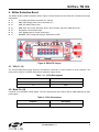
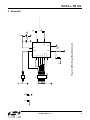
Si85xx-TB UG Si85 X X U N I D I R E C T I O N A L AC C U R R E N T S E N S O R TA R G E T B O A R D U S E R ’ S G U I D E The Si85xx products are unidirectional ac current sensors available with full scale current sense input ranges of 5, 10, and 20 A. Si85xx products are ideal upgrades for older current-sensing technologies offering size, performance and cost advantages over current transformers, Hall Effect devices, DCR circuits, and other approaches. The Si85xx are extremely low-loss, adding less than 1.3 mΩ of series resistance and less than 2 nH series inductance in the sensing path at 25 ºC. Current-sensing terminals are isolated from the other package pins to a maximum voltage of 1,000 VDC. 1. Kit Contents The Si85xx Unidirectional AC Current Sensor Development Kit contains the following items: 10 Amp Si8512 based evaluation board Si85xx Unidirectional AC Current Sensor Target Board User's Guide (this document) 2. Hardware Overview The Si85xx Target Board (Si85xx-TB, see Figure 1) provides a means to evaluate the ac current sensor in an existing application. It is meant to be soldered directly into the users existing power supply. The board comes with the Si8512 installed and provides a 10 Amp full scale input sense range and a 2.0 V full scale output voltage. For more details on the Si8512, refer to the Si85xx Data Sheet. Figure 1. Si85xx-TB Overview Rev. 0.1 6/07 Copyright © 2007 by Silicon Laboratories Si85xx-TB UG Si85xx-TB UG 3. Si85xx-TB Hardwired to Single-Phase POL Figure 2 illustrates the Si85xx-TB soldered directly into a single-phase POL. The single phase POL was designed to operate at a 400 kHz switch rate and provide better than 90 percent efficiency. It also provides 10 amps of peak current to the load and protects the supply by shutting down in the event of an over current condition. Figure 2. Si85xx-EVB Hardwired to Single-phase POL Figure 3 illustrates the Si8512 accurately monitoring the POL's switching current. As shown in the scope plot, a 1.6 V peak output voltage accurately monitors the 8 Amp peak, 50 percent duty cycle, 400 kHz current signal of the POL. A 20 mΩ sense resistor in series with the Si85xx is also monitored via a differential probe to provide a baseline measurement of the POL. Si8512 20 mΩ Sense Resistor Figure 3. Si85xx-TB OUT1 Oscilloscope Plot To accommodate this test, the Si85xx-TB was powered with a 5 V (100 mA) supply connected from J1 to J2. R1 was soldered from J4 to the respective phase control line of the POL. R2 and R4 were jumped to GND on J4. R3 was tied to 5 V and the Mode pin was jumped to VDD via J7. 2 Confidential Rev. 0.1 Si85xx-TB UG 4. Si85xx Evaluation Board The Si85xx-TB has a Si8512 installed. Refer to Figure 4 for the locations of the various I/O connectors and major components. J1 J2 J3 J4 J5 J6 J7 5 V Supply Input power connection 5 V, 100 mA GND, Input Supply power return connection, 0 V HDR-2X2, Mode Control input HDR-2X07, R1, R2, R3, R4 inputs, OUT1, OUT2 outputs, and seven GND return pins IIN Positive Current Sense Input IOUT Negative/return Current Sense Input HEADER, TRST timing select jumper, default tied to VDD Figure 4. Si85xx-TB Layout 4.1. VIN (J1, J2) The user-provided power supply should be connected to connectors J1 and J2 where J2 is the reference. The power source must be 5 V with at least 100 mA maximum output current. Table 1. J1, J2 Pin Descriptions Jumper # Description J1 5 V, 100 mA J2 GND 4.2. Mode Pin (J3) Connector J3 is the Mode Control header. The user should tie this pin to either VDD or GND depending on their power supply. Table 2. J3 Pin Descriptions Jumper # Description J3 VDD or GND Confidential Rev. 0.1 3 Si85xx-TB UG 4.3. R1, R2, R3, R4 Inputs, OUT1, OUT2 Outputs (J4) Connector J4 is used to provide the control inputs (R1, R2, R3, R4, MODE) to the Si85xx. It also provides the output voltage of the sensed input current on OUT1 and OUT2. Table 3. J4 Pin Descriptions Jumper # Description J4 R1, R2, R3, R4, OUT1, OUT2, GND 4.4. IIN (J5) Connector J5 is used to provide the positive current sense input to the Si85xx device. Table 4. J5 Pin Descriptions Jumper # Description J5 IIN 4.5. IOUT (J6) Connector J6 is used to provide the negative/return current sense input to the Si85xx device. Table 5. J6 Pin Descriptions Jumper # Description J6 IOUT 4.6. TRST RESET (J7) Connector J7 is used to set the timing for the Si85xx's integrator. J7 defaults to Reset option 1 where TRST is tied VDD providing approximately 200 ns of reset time. Reset option 2 is selected by connecting a timing resistor (R1 in Figure 4) from the TRST input to ground. Table 6. J7 Pin Descriptions 4 Jumper # Description J7 TRST – VDD or R1 to GND Confidential Rev. 0.1 V5V J1 5V Confidential Rev. 0.1 GND 1 3 5 7 9 11 13 1 3 2 4 6 8 10 12 14 2 4 MODE R1 R2 R3 R4 OUT1 OUT2 V5V 6 5 4 3 2 1 J7 Si851x OUT2 OUT1 R4 R3 R2 R1 U1 R1 DNP IOUT IIN Figure 5. Si85xx Target Board Schematic HDR-2X07 J4 J3 2 1 11 VDD 12 MODE TRST 7 GND 8 J2 V5V 9 10 C1 10uF V5V J6 IIOUT J5 IIN C2 0.1uF Normal Setup, No Mods Si85xx-TB UG 5. Schematic 5 Si85xx-TB UG 6. Bill of Materials Table 7. Si825x Multi-Phase POL Reference Design Bill of Materials 6 Item Quantity Reference Part Number Manufacturer Description 1 1 C1 PCC2182CT-ND Digi-Key 10 uF 2 1 C2 PCC1812CT-ND Digi-Key 0.1 uF 3 1 J1 2551-2-00-44-00-00-07-0 Bisco 5V 4 1 J2 2551-2-00-44-00-00-07-0 Bisco GND 5 1 J3 S2012-02-ND Digi-Key HDR-2X2 6 1 J4 S2012-07-ND Digi-Key HDR-2X07 7 1 J5 2551-2-00-44-00-00-07-0 Bisco IIN 8 1 J6 2551-2-00-44-00-00-07-0 Bisco IIOUT 9 1 J7 S1012-02-ND Digi-Key HEADER 10 1 R1 P150CCT-ND Digi-Key DNP 11 1 U1 Si8512-IS Digi-Key Si851x Confidential Rev. 0.1 Si85xx-TB UG NOTES: Confidential Rev. 0.1 7 Si85xx-TB UG CONTACT INFORMATION Silicon Laboratories Inc. 400 West Cesar Chavez Austin, TX 78701 Tel: 1+(512) 416-8500 Fax: 1+(512) 416-9669 Toll Free: 1+(877) 444-3032 Email: [email protected] Internet: www.silabs.com The information in this document is believed to be accurate in all respects at the time of publication but is subject to change without notice. Silicon Laboratories assumes no responsibility for errors and omissions, and disclaims responsibility for any consequences resulting from the use of information included herein. Additionally, Silicon Laboratories assumes no responsibility for the functioning of undescribed features or parameters. Silicon Laboratories reserves the right to make changes without further notice. Silicon Laboratories makes no warranty, representation or guarantee regarding the suitability of its products for any particular purpose, nor does Silicon Laboratories assume any liability arising out of the application or use of any product or circuit, and specifically disclaims any and all liability, including without limitation consequential or incidental damages. Silicon Laboratories products are not designed, intended, or authorized for use in applications intended to support or sustain life, or for any other application in which the failure of the Silicon Laboratories product could create a situation where personal injury or death may occur. Should Buyer purchase or use Silicon Laboratories products for any such unintended or unauthorized application, Buyer shall indemnify and hold Silicon Laboratories harmless against all claims and damages. The sale of this product contains no licenses to Power-One’s intellectual property. Contact Power-One, Inc. for appropriate licenses. Silicon Laboratories and Silicon Labs are trademarks of Silicon Laboratories Inc. Other products or brandnames mentioned herein are trademarks or registered trademarks of their respective holders. 8 Confidential Rev. 0.1