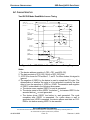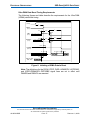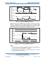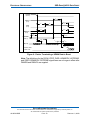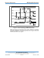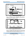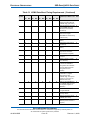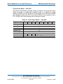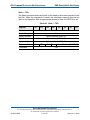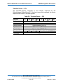
1
DATA SHEET
SILICONDRIVE EP 2.5" PATA DRIVE
SSD-DXXX(I)-4210
OVERVIEW
FEATURES
The SiliconDrive EP 2.5" PATA Drive is an
optimal time-to-market replacement for
hard drives and flash cards or in host
systems that require low power and
scalable storage solutions.
• RoHS 6 of 6 compliant
• Integrated PowerArmor and SiSMART
technology
• Capacity range: 16GB to 64GB
• Supports 5V interface
• MTBF 4,000,000 hours
• ATA-5 compliant
• Industry standard 2.5" Drive form factor
• Supports UDMA modes 0-4
SiliconDrive EP technology is engineered
exclusively for the high performance, high
reliability and multi-year product lifecycle
requirements of the Enterprise System
OEM
market.
Typical
end-market
applications include broadband data and
voice networks, military systems, flight
system avionics, medical equipment,
industrial
control
systems,
video
surveillance, storage networking, VoIP,
wireless infrastructure, and interactive
kiosks.
Every SiliconDrive EP is integrated with
SiliconSystems patented PowerArmor and
patent-pending SiSMART to virtually
eliminate storage systems failures.
PowerArmor prevents data corruption and
loss from power disturbances by
integrating patented technology into every
SiliconDrive EP.
SiSMART acts as an early warning system
to eliminate unscheduled downtime by
constantly monitoring and reporting the
exact amount of remaining storage system
useful life.
Numerous SiliconSystems patented and
patent-pending
application-specific
technology can be integrated into
SiliconDrive EP to safeguard application
data and software IP. Application notes
detailing these performance-enhancing
options are available under NDA.
Click here
Click here
SILICONSYSTEMS PROPRIETARY
This document and the information contained within it is confidential and proprietary to SiliconSystems, Inc.
All unauthorized use and/or reproduction is prohibited.
26840 ALISO VIEJO PARKWAY, ALISO VIEJO, CA 92656
4210D-03DSR
• PHONE: 949.900.9400 • FAX: 949.900.9500 • http://www.siliconsystems.com
FEBRUARY 2, 2009
REVISION HISTORY
SSD-DXXX(I)-4210 DATA SHEET
REVISION HISTORY
Document No.
Release Date
Changes
4210D-03DSR
February 2, 2009
4210D-02DSR
4210D-01DSR
PRELIMINARY
4210D-00DSR
PRELIMINARY
December 15, 2008
September 25, 2008
Updated:
• "System Reliability" table and changed the
name to "Reliability."
• "Related Documentation" table.
Added:
• “Projected Operational Life Span.”
External release with internal updates.
Internal updates.
September 16, 2008
Initial internal release.
SILICONSYSTEMS PROPRIETARY
This document and the information contained within it is confidential and proprietary to SiliconSystems, Inc.
All unauthorized use and/or reproduction is prohibited.
4210D-03DSR
PAGE II
FEBRUARY 2, 2009
TABLE OF CONTENTS
SSD-DXXX(I)-4210 DATA SHEET
TABLE OF CONTENTS
Overview .......................................................................................................................... i
Features ........................................................................................................................... i
Revision History..............................................................................................................II
List of Figures ................................................................................................................VI
List of Tables ................................................................................................................. VII
Physical Specifications ................................................................................................. 1
Physical Dimensions .................................................................................................... 1
Pin Locations................................................................................................................ 2
Jumper Settings ........................................................................................................... 2
Product Specifications .................................................................................................. 3
System Performance.................................................................................................... 3
System Power Requirements....................................................................................... 3
Reliability ...................................................................................................................... 4
Projected Operational Life Span .................................................................................. 4
Product Capacity Specifications................................................................................... 5
Environmental Specifications ....................................................................................... 5
Electrical Specification.................................................................................................. 6
Pin Assignments........................................................................................................... 6
Signal Descriptions....................................................................................................... 7
Absolute Maximum Ratings........................................................................................ 11
DC Characteristics ..................................................................................................... 12
AC Characteristics...................................................................................................... 13
True IDE PIO Mode Read/Write Access Timing .................................................. 13
True IDE Multiword DMA Read/Write Access Timing .......................................... 15
Ultra DMA Data Burst Timing Requirements........................................................ 17
ATA and True IDE Register Decoding ........................................................................ 27
Task File Register Specification ................................................................................. 27
SILICONSYSTEMS PROPRIETARY
This document and the information contained within it is confidential and proprietary to SiliconSystems, Inc.
All unauthorized use and/or reproduction is prohibited.
4210D-03DSR
PAGE III
FEBRUARY 2, 2009
TABLE OF CONTENTS
SSD-DXXX(I)-4210 DATA SHEET
ATA Registers............................................................................................................... 28
Data Register ............................................................................................................. 28
Error Register ............................................................................................................. 28
Feature Register......................................................................................................... 29
Sector Count Register ................................................................................................ 30
Sector Number Register............................................................................................. 31
Cylinder Low Register ................................................................................................ 32
Cylinder High Register ............................................................................................... 33
Drive/Head Register ................................................................................................... 34
Status Register........................................................................................................... 35
Command Register .................................................................................................... 36
Alternate Status Register ........................................................................................... 37
Device Control Register ............................................................................................. 38
Device Address Register............................................................................................ 39
ATA Command Block and Set Description ................................................................ 40
ATA Command Set .................................................................................................... 40
Check Power Mode — 98h, E5h .......................................................................... 42
Executive Drive Diagnostic — 90h ....................................................................... 43
Format Track — 50h ............................................................................................ 44
Identify Drive — ECh............................................................................................ 45
Identify Drive — Drive Attribute Data ............................................................. 46
Idle — 97h, E3h.................................................................................................... 49
Idle Immediate — 95h, E1h.................................................................................. 50
Initialize Drive Parameters — 91h........................................................................ 51
Recalibrate — 1Xh ............................................................................................... 52
Read Buffer — E4h .............................................................................................. 53
Read DMA — C8h................................................................................................ 54
Read Multiple — C4h ........................................................................................... 55
Read Sector — 20h, 21h...................................................................................... 56
SILICONSYSTEMS PROPRIETARY
This document and the information contained within it is confidential and proprietary to SiliconSystems, Inc.
All unauthorized use and/or reproduction is prohibited.
4210D-03DSR
PAGE IV
FEBRUARY 2, 2009
TABLE OF CONTENTS
SSD-DXXX(I)-4210 DATA SHEET
Read Long Sector(s) — 22h, 23h......................................................................... 57
Read Verify Sector(s) — 40h, 41h ....................................................................... 58
Seek — 7Xh ......................................................................................................... 59
Set Features — EFh............................................................................................. 60
Set Multiple Mode — C6h .................................................................................... 61
Set Sleep Mode — 99h, E6h................................................................................ 62
Standby — 96h, E2h ............................................................................................ 63
Standby Immediate — 94h, E0h .......................................................................... 64
Write Buffer — E8h .............................................................................................. 65
Write DMA — CAh ............................................................................................... 66
Write Multiple — C5h ........................................................................................... 67
Write Sector(s) — 30h, 31h.................................................................................. 68
Write Long Sector(s) — 32h, 33h......................................................................... 69
Erase Sector(s) — C0h ........................................................................................ 70
Request Sense — 03h ......................................................................................... 71
Translate Sector — 87h ....................................................................................... 72
Wear-Level — F5h ............................................................................................... 73
Write Multiple w/o Erase — CDh.......................................................................... 74
Write Sector(s) w/o Erase — 38h......................................................................... 75
Write Verify — 3Ch............................................................................................... 76
Sales and Support ....................................................................................................... 77
Part Numbering ............................................................................................................ 77
Nomenclature ............................................................................................................. 77
Part Numbers ............................................................................................................. 77
RoHS 6 of 6 Product Labeling — Pb-Free Identification Label .................................. 78
Sample Label ............................................................................................................. 78
Related Documentation............................................................................................... 79
SILICONSYSTEMS PROPRIETARY
This document and the information contained within it is confidential and proprietary to SiliconSystems, Inc.
All unauthorized use and/or reproduction is prohibited.
4210D-03DSR
PAGE V
FEBRUARY 2, 2009
LIST OF FIGURES
SSD-DXXX(I)-4210 DATA SHEET
LIST OF FIGURES
Figure 1: Physical Dimensions......................................................................................... 1
Figure 2: Pin Locations .................................................................................................... 2
Figure 3: Jumper Settings................................................................................................ 2
Figure 4: True IDE PIO Mode Read/Write Access Timing Diagram .............................. 13
Figure 5: True IDE Multiword DMA Read/Write Access Timing..................................... 15
Figure 6: Initiating a UDMA Data-In Burst...................................................................... 17
Figure 7: Sustained UDMA Data-In Burst ...................................................................... 18
Figure 8: Host Pausing a UDMA Data-In Burst.............................................................. 18
Figure 9: Device Terminating a UDMA Data-In Burst .................................................... 19
Figure 10: Host Terminating a UDMA Data-In Burst...................................................... 20
Figure 11: Initiating a UDMA Data-Out Burst................................................................. 21
Figure 12: Sustained UDMA Data-Out Burst ................................................................. 21
Figure 13: Device Pausing a UDMA Data-Out Burst ..................................................... 22
Figure 14: Host Terminating a UDMA Data-Out Burst................................................... 23
Figure 15: Device Terminating a UDMA Data-Out Burst ............................................... 24
Figure 16: Sample Label................................................................................................ 78
SILICONSYSTEMS PROPRIETARY
This document and the information contained within it is confidential and proprietary to SiliconSystems, Inc.
All unauthorized use and/or reproduction is prohibited.
4210D-03DSR
PAGE VI
FEBRUARY 2, 2009
LIST OF TABLES
SSD-DXXX(I)-4210 DATA SHEET
LIST OF TABLES
Table 1: System Performance ......................................................................................... 3
Table 2: System Power Requirements ............................................................................ 3
Table 3: Reliability............................................................................................................ 4
Table 4: Operational Life Span ........................................................................................ 4
Table 5: Product Capacity Specifications ........................................................................ 5
Table 6: Environmental Specifications............................................................................. 5
Table 7: Pin Assignments ................................................................................................ 6
Table 8: Signal Descriptions ............................................................................................ 7
Table 9: Absolute Maximum Ratings ............................................................................. 11
Table 10: DC Characteristics ......................................................................................... 12
Table 11: True IDE PIO Mode Read/Write Access Timing ............................................ 14
Table 12: True IDE Multiword DMA Read/Write Access Timing.................................... 16
Table 13: UDMA Data Burst Timing Requirements ....................................................... 24
Table 14: Task File Register Specification..................................................................... 27
Table 15: Error Register................................................................................................. 28
Table 16: Feature Register ............................................................................................ 29
Table 17: Sector Count Register.................................................................................... 30
Table 18: Sector Number Register ................................................................................ 31
Table 19: Cylinder Low Register.................................................................................... 32
Table 20: Cylinder High Register ................................................................................... 33
Table 21: Drive/Head Register....................................................................................... 34
Table 22: Status Register .............................................................................................. 35
Table 23: Command Register ........................................................................................ 36
Table 24: Alternate Status Register ............................................................................... 37
Table 25: Device Control Register ................................................................................. 38
Table 26: Device Address Register ............................................................................... 39
Table 27: ATA Command Block and Set Description .................................................... 40
SILICONSYSTEMS PROPRIETARY
This document and the information contained within it is confidential and proprietary to SiliconSystems, Inc.
All unauthorized use and/or reproduction is prohibited.
4210D-03DSR
PAGE VII
FEBRUARY 2, 2009
LIST OF TABLES
SSD-DXXX(I)-4210 DATA SHEET
Table 28: ATA Command Set ........................................................................................ 40
Table 29: Check Power Mode — 98h, E5h.................................................................... 42
Table 30: Executive Drive Diagnostic — 90h................................................................. 43
Table 31: Format Track — 50h ...................................................................................... 44
Table 32: Identify Drive — ECh ..................................................................................... 45
Table 33: Identify Drive — Drive Attribute Data ............................................................. 46
Table 34: Idle — 97h, E3h ............................................................................................. 49
Table 35: Idle Immediate — 95h, E1h ........................................................................... 50
Table 36: Initialize Drive Parameters — 91h ................................................................. 51
Table 37: Recalibrate — 1Xh......................................................................................... 52
Table 38: Read Buffer — E4h........................................................................................ 53
Table 39: Read DMA — C8h ......................................................................................... 54
Table 40: Read Multiple — C4h..................................................................................... 55
Table 41: Read Sector — 20h, 21h ............................................................................... 56
Table 42: Read Long Sector(s) — 22h, 23h .................................................................. 57
Table 43: Read Verify Sector(s) — 40h, 41h ................................................................. 58
Table 44: Seek — 7Xh................................................................................................... 59
Table 45: Set Features — EFh ...................................................................................... 60
Table 46: Set Features’ Attributes ................................................................................. 60
Table 47: Set Multiple Mode — C6h .............................................................................. 61
Table 48: Set Sleep Mode — 99h, E6h ......................................................................... 62
Table 49: Standby — 96h, E2h...................................................................................... 63
Table 50: Standby Immediate — 94h, E0h .................................................................... 64
Table 51: Write Buffer — E8h ........................................................................................ 65
Table 52: Write DMA — CAh ......................................................................................... 66
Table 53: Write Multiple — C5h ..................................................................................... 67
Table 54: Write Sector(s) — 30h, 31h ........................................................................... 68
Table 55: Write Long Sector(s) — 32h, 33h .................................................................. 69
Table 56: Erase Sector(s) — C0h.................................................................................. 70
SILICONSYSTEMS PROPRIETARY
This document and the information contained within it is confidential and proprietary to SiliconSystems, Inc.
All unauthorized use and/or reproduction is prohibited.
4210D-03DSR
PAGE VIII
FEBRUARY 2, 2009
LIST OF TABLES
SSD-DXXX(I)-4210 DATA SHEET
Table 57: Request Sense — 03h................................................................................... 71
Table 58: Extended Error Codes ................................................................................... 71
Table 59: Translate Sector — 87h ................................................................................. 72
Table 60: Wear-Level — F5h......................................................................................... 73
Table 61: Write Multiple w/o Erase — CDh ................................................................... 74
Table 62: Write Sector(s) w/o Erase — 38h .................................................................. 75
Table 63: Write Verify — 3Ch ........................................................................................ 76
Table 64: Part Numbering Nomenclature ...................................................................... 77
Table 65: Part Numbers................................................................................................. 77
Table 66: Related Documentation ................................................................................. 79
SILICONSYSTEMS PROPRIETARY
This document and the information contained within it is confidential and proprietary to SiliconSystems, Inc.
All unauthorized use and/or reproduction is prohibited.
4210D-03DSR
PAGE IX
FEBRUARY 2, 2009
PHYSICAL SPECIFICATIONS
SSD-DXXX(I)-4210 DATA SHEET
PHYSICAL SPECIFICATIONS
The SiliconDrive EP 2.5" PATA Drive products are offered in an industrystandard 2.5" PATA Drive form factor. See "Part Numbering" on page 77 for
details regarding 2.5" PATA Drive capacities.
PHYSICAL DIMENSIONS
This section provides diagrams that describe the physical dimensions for the
2.5" PATA Drive.
Figure 1: Physical Dimensions
Dimension Millimeters Tolerance (mm)
Dimension Millimeters Tolerance (mm)
A
B
C
D
E
F
G
H
I
J
K
L
M
N
P
Q
R
S
T
U
V
W
100.00
90.60
73.03
34.93
14.00
4.08
61.70
4.68
64.42
10.14
3.99
±0.25
±0.125
±0.125
±0.125
±0.125
±0.125
±0.125
±0.125
±0.125
±0.51
±0.43
69.85
2.00
9.40
6.00
11.57
32.10
14.93
11.00
4.65
4.00
6.15
±0.25
±0.125
±0.10
±0.125
±0.125
±0.125
±0.125
±0.125
±0.125
±0.125
±0.125
SILICONSYSTEMS PROPRIETARY
This document and the information contained within it is confidential and proprietary to SiliconSystems, Inc.
All unauthorized use and/or reproduction is prohibited.
4210D-03DSR
PAGE 1
FEBRUARY 2, 2009
PHYSICAL SPECIFICATIONS
SSD-DXXX(I)-4210 DATA SHEET
PIN LOCATIONS
The following diagram identifies the pin locations of the 2.5" PATA Drive.
Figure 2: Pin Locations
JUMPER SETTINGS
The following diagram defines the SiliconDrive EP 2.5" PATA Drive jumper
settings.
Figure 3: Jumper Settings
SILICONSYSTEMS PROPRIETARY
This document and the information contained within it is confidential and proprietary to SiliconSystems, Inc.
All unauthorized use and/or reproduction is prohibited.
4210D-03DSR
PAGE 2
FEBRUARY 2, 2009
PRODUCT SPECIFICATIONS
SSD-DXXX(I)-4210 DATA SHEET
PRODUCT SPECIFICATIONS
Note: All SiliconDrive EP 2.5" PATA Drive values quoted are typical at
25°C and nominal supply voltage.
SYSTEM PERFORMANCE
Table 1: System Performance
Reset to Ready Startup Time (Typical/Maximum)
Read Transfer Rate (Typical)
Write Transfer Rate (Typical)
Burst Transfer Rate
Controller Overhead (Command to DRQ)
200ms/400ms
50MBps
50MBps
66MBps
2ms (maximum)
SYSTEM POWER REQUIREMENTS
Table 2: System Power Requirements
DC Input Voltage
Sleep (Standby Current)
Read (/Peak)
Write (/Peak)
5.0 ± 10%
100mA
200mA
300mA
SILICONSYSTEMS PROPRIETARY
This document and the information contained within it is confidential and proprietary to SiliconSystems, Inc.
All unauthorized use and/or reproduction is prohibited.
4210D-03DSR
PAGE 3
FEBRUARY 2, 2009
PRODUCT SPECIFICATIONS
SSD-DXXX(I)-4210 DATA SHEET
RELIABILITY
Table 3: Reliability
MTBF (@ 25ºC)
4,000,000 hours
Bit Error Rate
<1 non-recoverable error in 1014 bits read
PROJECTED OPERATIONAL LIFE SPAN
Table 4: Operational Life Span
SiliconDrive Part#
Capacity
Service Life*
GB Written per Day
SSD-D64G-4210
64GB
17.9 Years
@ 978.5GB
SSD-D32G-4210
SSD-D16G-4210
32GB
16GB
9.0 Years
4.5 Years
@ 978.5GB
@ 978.5GB
* There are unlimited read cycles. Service life is determined using
SiliconSystems’ LifeEst calculation at 100% duty cycle with 25% write cycles.
LifeEst is a comprehensive measurement that considers numerous factors to
determine the projected life span of a SiliconDrive. A white paper that
describes the benefits of LifeEst and how to calculate it can be found at http://
www.siliconsystems.com/resources/Documents/Whitepaper/
SiliconSystems_NAND_Evolution.pdf.
The actual life of a SiliconDrive is dependant on the customer usage model.
SiSMART is a patented technology of SiliconSystems that enables host
systems to monitor actual usage of a SiliconDrive in real time. SiSMART
measures and reports the remaining life of a SiliconDrive. For more
information on SiSMART, refer to the Eliminating Unscheduled Downtime by
Forecasting Useable Life white paper at http://www.siliconsystems.com/
technology/pdfs/SiliconDrive_SiSMART.pdf.
SILICONSYSTEMS PROPRIETARY
This document and the information contained within it is confidential and proprietary to SiliconSystems, Inc.
All unauthorized use and/or reproduction is prohibited.
4210D-03DSR
PAGE 4
FEBRUARY 2, 2009
PRODUCT SPECIFICATIONS
SSD-DXXX(I)-4210 DATA SHEET
PRODUCT CAPACITY SPECIFICATIONS
Table 5: Product Capacity Specifications
Product Capacity
Capacity (Bytes)
16GB
32GB
64GB
Number of
Sectors
Number of
Number of Number
Sectors/
Cylinders of Heads
Track
16,391,208,960 32,014,080 16,383*
32,782,417,920 64,028,160 16,383*
65,564,835,840 128,056,320 16,383*
16
16
16
63
63
63
* = All IDE drives 8GB and larger use 16383 cylinders, 16 heads, and 63 sectors/track due to
interface restrictions.
ENVIRONMENTAL SPECIFICATIONS
Table 6: Environmental Specifications
Temperature
Humidity
Vibration
Shock
Altitude
0ºC to 70ºC (Commercial)
-40ºC to 85ºC (Industrial)
8% to 95% non-condensing
16.3gRMS, MIL-STD-810F, Method 514.5, Procedure I,
Category 24
1000G, Half-sine, 0.5ms Duration
50g Pk, MIL-STD-810F, Method 516.5, Procedure I
80,000ft, MIL-STD-810F, Method 500.4, Procedure II
SILICONSYSTEMS PROPRIETARY
This document and the information contained within it is confidential and proprietary to SiliconSystems, Inc.
All unauthorized use and/or reproduction is prohibited.
4210D-03DSR
PAGE 5
FEBRUARY 2, 2009
ELECTRICAL SPECIFICATION
SSD-DXXX(I)-4210 DATA SHEET
ELECTRICAL SPECIFICATION
PIN ASSIGNMENTS
The following table describes the SiliconDrive EP 2.5" PATA Drive 44-pin IDE
connector signals.
Table 7: Pin Assignments
Pin
IDE-ATA
Ultra DMA
Pin
IDE-ATA
Ultra DMA
1
3
5
7
9
11
13
15
17
19
RESET#
D7
D6
D5
D4
D3
D2
D1
D0
GND
RESET#
D7
D6
D5
D4
D3
D2
D1
D0
GND
2
4
6
8
10
12
14
16
18
20
GND
D8
D9
D10
D11
D12
D13
D14
D15
KEY
GND
D8
D9
D10
D11
D12
D13
D14
D15
KEY
21
23
DMARQ
IOWR#
22
24
GND
GND
GND
GND
25
IORD#
26
GND
GND
27
IORDY
28
CSEL#
CSEL#
29
31
33
35
37
39
DMACK#
INTRQ
A1
A0
CS0#
DASP#
DMARQ#
STOP
HDSTROBE
HDMARDY#
DDSTROBE
DDMARDY#
DMACK#
INTRQ
A1
A0
CS0#
DASP
30
32
34
36
38
40
GND
IOCS16#
PDIAG#
A2
CS1#
GND
GND
IOCS16#
PDIAG#
A2
CS1#
GND
SILICONSYSTEMS PROPRIETARY
This document and the information contained within it is confidential and proprietary to SiliconSystems, Inc.
All unauthorized use and/or reproduction is prohibited.
4210D-03DSR
PAGE 6
FEBRUARY 2, 2009
ELECTRICAL SPECIFICATION
SSD-DXXX(I)-4210 DATA SHEET
SIGNAL DESCRIPTIONS
Table 8: Signal Descriptions
Signal Name
Pin(s)
Type Description
A2-A0
36, 33,
35
I
-CS0,-CS1
37, 38
I
-CSEL
28
I
Address Inputs. These signals are
asserted by the host to access the task
registers in the device.
In the true IDE mode, -CS0 is the chip
select for the task file registers while -CS1
is used to select the Alternate Status
register and the Device Control register.
Cable Select. This internally pulled-up
signal is used to configure this device as a
master or a slave when the jumper
configuration is in CSEL mode.
When this pin is:
• Grounded by the host, this device is
configured as a master.
• Open, this device is configured as a
slave.
D15-D0
-DMACK
18, 16,
I/O
14, 12,
10, 8, 6,
4, 3, 5, 7,
9, 11, 13,
15, 17
29
I
DASP
39
I/O
Data Inputs/Outputs. This is the 8-bit or
16-bit bidirectional interface between the
host and device. The lower eight bits are
used for 8-bit register transfers.
DMA Acknowledge. This signal is used by
the host in response to DMARQ to initiate
DMA transfers. The DMARQ/-DMACK
handshake is used to provide flow control
during the transfer. When -DMACK is
asserted, -CS0 and -CS1 are not asserted
and transfers are 16-bits wide.
Disk Active/Slave Present. This open
drain output signal is asserted low any time
the drive is active. In a master/slave
configuration, this signal is used by the
slave to inform the master that a slave is
present.
SILICONSYSTEMS PROPRIETARY
This document and the information contained within it is confidential and proprietary to SiliconSystems, Inc.
All unauthorized use and/or reproduction is prohibited.
4210D-03DSR
PAGE 7
FEBRUARY 2, 2009
ELECTRICAL SPECIFICATION
SSD-DXXX(I)-4210 DATA SHEET
Table 8: Signal Descriptions (Continued)
Signal Name
Pin(s)
Type Description
DMARQ
21
O
DMA Request. This signal is used for DMA
transfers between the host and device.
DMARQ is asserted by the device when the
device is ready to transfer data to/from the
host. The direction of data transfer is
controller by -IORD and -IOWR. This signal
is used in a handshake manner with DMACK (i.e., the device waits until the host
asserts -DMACK before negating DMARQ,
and reasserts DMARQ if there is more data
to transfer). The DMARQ/-DMACK
handshake is used to provide flow control
during the transfer.
SILICONSYSTEMS PROPRIETARY
This document and the information contained within it is confidential and proprietary to SiliconSystems, Inc.
All unauthorized use and/or reproduction is prohibited.
4210D-03DSR
PAGE 8
FEBRUARY 2, 2009
ELECTRICAL SPECIFICATION
SSD-DXXX(I)-4210 DATA SHEET
Table 8: Signal Descriptions (Continued)
Signal Name
Pin(s)
Type Description
DMARQ#
(UDMA
protocol
active)
GND
INTRQ
2, 19, 22, 24, 26,
30, 40,
43
31
O
This signal is a DMA request that is used
for DMA data transfers between the host
and device. This signal is asserted by the
device when it is ready to transfer data to or
from the host.
For Multiword DMA transfers, the direction
of data transfer is controlled by -IORD and
-IOWR. This signal is used in a handshake
manner with -DMACK (i.e., the device waits
until the host asserts (-)DMACK before
negating (-)DMARQ, and reasserts
(-)DMARQ if there is more data to transfer).
In PCMCIA I/O mode, the -DMARQ is
ignored by the host while the host is
performing an I/O Read cycle to the device.
The host does not initiate an I/O Read cycle
while -DMARQ is asserted by the device.
In True IDE mode, DMARQ is not driven
when the device is not selected in the
Drive-Head register.
While a DMA operation is in progress, -CS0
(-CE1) and -CS1 (-CE2) are held negated
and the width of the transfers is 16 bits.
If there is no hardware support for True IDE
DMA mode in the host, this output signal is
not used and should not be connected at
the host. In this case, the BIOS must report
that DMA mode is not supported by the
host so that device drivers do not attempt
the DMA mode operation.
Ground. The device ground signal.
Interrupt Request. This signal is an active
high interrupt request to the host.
SILICONSYSTEMS PROPRIETARY
This document and the information contained within it is confidential and proprietary to SiliconSystems, Inc.
All unauthorized use and/or reproduction is prohibited.
4210D-03DSR
PAGE 9
FEBRUARY 2, 2009
ELECTRICAL SPECIFICATION
SSD-DXXX(I)-4210 DATA SHEET
Table 8: Signal Descriptions (Continued)
Signal Name
Pin(s)
Type Description
IORDY
(True IDE
mode)
-IORD
(True IDE
mode)
27
I
I/O Channel Ready. The signal is negated
to extend the host transfer cycle of any host
register access.
25
I
Device I/O Read. This is the read strobe
signal from the host. The falling edge of
IORD enables data from the device onto
the data bus. The rising edge of IORD
latches data at the host. The host does not
act on the data until it is latched.
When UDMA mode DMA write is active in
all modes, this signal is asserted by the
device during a data burst to indicate that
the device is ready to receive UDMA dataout bursts.
The device may negate -DDMARDY to
pause a UDMA transfer.
-DDMARDY
(UDMA write
protocol
active)
DSTROBE
(UDMA read
protocol
active)
-IOWR
(True IDE
mode)
-HDMARDY
(UDMA read
protocol
active)
23
I
When UDMA mode DMA read is active in
all modes, this signal is the data in strobe
generated by the device. Both the rising
and falling edge of DSTROBE cause data
to be latched by the host. The device may
stop generating DSTROBE edges to pause
a UDMA data-in burst.
Device I/O Write. This is the write strobe
signal from the host. The rising edge of
IOWR# latches data from the data bit
signals. The device does not act on the
data until it is latched.
When UDMA mode DMA read is active in
all modes, this signal is asserted by the
host to indicate that the host is ready to
receive UDMA data-in bursts. The host may
negate -HDMARDY to pause a UDMA
transfer.
SILICONSYSTEMS PROPRIETARY
This document and the information contained within it is confidential and proprietary to SiliconSystems, Inc.
All unauthorized use and/or reproduction is prohibited.
4210D-03DSR
PAGE 10
FEBRUARY 2, 2009
ELECTRICAL SPECIFICATION
SSD-DXXX(I)-4210 DATA SHEET
Table 8: Signal Descriptions (Continued)
Signal Name
Pin(s)
Type Description
HDSTROBE
(UDMA write
protocol
active)
When UDMA mode DMA write is active in
all modes, this signal is the data-out strobe
generated by the host. Both the rising and
falling edge of HSTROBE cause data to be
latched by the device. The host may stop
generating HSTROBE edges to pause an
UDMA data-out burst.
Key. Reserved for the Connector Key.
While the UDMA mode protocol is active in
all modes, the assertion of this signal
causes the termination of the UDMA data
burst.
KEY
STOP
(UDMA
protocol
active)
-PDIAG
20
-
34
I/O
-RESET
1
I
VCC
41, 42
-
Pass Diagnostic. This open drain signal is
asserted by the slave to indicate to the
master that it has passed its diagnostics.
Device Reset. An active low signal. When
active, this signal sets all internal registers
to their default state. This signal is held
asserted until at least 25μs after power has
been stabilized during the device power-on.
Device Power Supply. The device power
+3.3V/5V signal.
ABSOLUTE MAXIMUM RATINGS
Table 9: Absolute Maximum Ratings
Symbol
Parameter
Minimum
Maximum Units
TS
Storage Temperature
-55
125
°C
TA
Operating Temperature
-40
85
°C
VCC
VCC with Respect to GND
-0.5
VCC + 0.5 V
VIN
Input Voltage
-0.3
VCC + 0.3 V
VOUT
Output Voltage
-
6.0
V
SILICONSYSTEMS PROPRIETARY
This document and the information contained within it is confidential and proprietary to SiliconSystems, Inc.
All unauthorized use and/or reproduction is prohibited.
4210D-03DSR
PAGE 11
FEBRUARY 2, 2009
ELECTRICAL SPECIFICATION
SSD-DXXX(I)-4210 DATA SHEET
DC CHARACTERISTICS
Table 10: DC Characteristics
5V ± 10%
Symbol
Parameter
Units
Minimum
Maximum
ILI
Input Leakage *(1) Current
-
10
μA
ILO
Output Leakage *(1) Current -
10
μA
ICCR
ICC Read Current
-
100
mA
ICCW
ICC Write Current
-
200
mA
ICCS
ICC Standby Current
-
15
mA
SILICONSYSTEMS PROPRIETARY
This document and the information contained within it is confidential and proprietary to SiliconSystems, Inc.
All unauthorized use and/or reproduction is prohibited.
4210D-03DSR
PAGE 12
FEBRUARY 2, 2009
ELECTRICAL SPECIFICATION
SSD-DXXX(I)-4210 DATA SHEET
AC CHARACTERISTICS
True IDE PIO Mode Read/Write Access Timing
ADDR valid
(A02, A01, A00, -CS0, -CS1)
note 1)
1)
(See note
t0
t1
t2
t9
t8
t 2i
-IORD / -IOWR
Write
Data (D15:D00)
(See
note 2)
2)
(See note
t3
t4
t5
t6
Read
Data (D15:D00)
(See
note 2)
2)
(See note
t7
t 6z
-IOCS16
(See note 3)
IORDY
(See note
note 4,
4a)4-1)
tA
IORDY
(See note
note 4,
4b)
4-2)
tC
t RD
IORDY
(See note
note 4,
4c)4-3)
tB
tC
Figure 4: True IDE PIO Mode Read/Write Access Timing Diagram
Notes:
1. The device address consists of -CS0, -CS1, and A[02::00].
2. The data consists of D[15::00] (16-bit) or D[07::00] (8 bit).
3. -IOCS16 is shown for PIO modes 0, 1, and 2. For other modes, this signal is
ignored.
4. The negation of IORDY by the device is used to extend the PIO cycle. The
determination of whether the cycle is to be extended is made by the host
after tA from the assertion of -IORD or -IOWR. The assertion and negation
of IORDY is described in the following three cases:
a. The device never negates IORDY; no wait is generated.
b. The device starts to drive IORDY low before tA, but causes IORDY to be
asserted before tA; no wait generated.
c. The device drives IORDY low before tA; wait generated. The cycle
completes after IORDY is reasserted. For cycles where a wait is
generated and -IORD is asserted, the device places read data on D15D00 for tRD before causing IORDY to be asserted.
SILICONSYSTEMS PROPRIETARY
This document and the information contained within it is confidential and proprietary to SiliconSystems, Inc.
All unauthorized use and/or reproduction is prohibited.
4210D-03DSR
PAGE 13
FEBRUARY 2, 2009
ELECTRICAL SPECIFICATION
SSD-DXXX(I)-4210 DATA SHEET
Table 11: True IDE PIO Mode Read/Write Access Timing
Symbol Item
Mode 0 Mode 1 Mode 2 Mode 3 Mode 4 Mode 5 Mode 6 Note Units
t0
Cycle Time (minimum)
600
383
240
180
120
100
80
1
ns
t1
Address Valid to
IORD/-IOWR Setup
(minimum)
70
50
30
30
25
15
10
-
ns
t2
-IORD/-IOWR (minimum) 165
125
100
80
70
65
55
1
ns
t2
-IORD/-IOWR (minimum) 290
register (8 bit)
290
290
80
70
65
55
1
ns
t2i
-IORD/-IOWR Recovery
Time (minimum)
-
-
-
70
25
25
20
1
ns
t3
-IOWR Data Setup
(minimum)
60
45
30
30
20
20
15
-
ns
t4
-IOWR Data Hold
(minimum)
30
20
15
10
10
5
5
-
ns
t5
-IORD Data Setup
(minimum)
50
35
20
20
20
15
10
-
ns
t6
-IORD Data Hold
(minimum)
5
5
5
5
5
5
5
-
ns
t6Z
-IORD Data Tristate
(maximum)
30
30
30
30
30
20
20
2
ns
t7
Address Valid to IOCS16
Assertion (maximum)
90
50
40
N/A
N/A
N/A
N/A
4
ns
t8
Address Valid to IOCS16
Released (maximum)
60
45
30
N/A
N/A
N/A
N/A
4
ns
t9
-IORD/-IOWR to
Address Valid Hold
20
15
10
10
10
10
10
-
ns
tRD
Read Data Valid to
IORDY Active
(minimum), if IORDY is
initially low after tA
0
0
0
0
0
0
0
-
ns
tA
IORDY Setup Time
35
35
35
35
35
N/A5
N/A5
3
ns
tB
IORDY Pulse Width
(maximum)
1250
1250
1250
1250
1250
5
N/A
5
N/A
-
ns
tC
IORDY Assertion to
Release (maximum)
5
5
5
5
5
N/A5
N/A5
-
ns
Notes:
1. The symbol t0 is the minimum total cycle time, t2 is the minimum command
active time, and t2i is the minimum command recovery time or command
inactive time. The actual cycle time equals the sum of the actual command
active time and the actual command inactive time. The three timing
requirements of t0, t2, and t2i must be met. The minimum total cycle time
requirement is greater than the sum of t2 and t2i. This means a host
implementation can lengthen either or both t2 or t2i to ensure that t0 is equal
to or greater than the value reported in the device’s identify device data.
2. This parameter specifies the time from the negation edge of -IORD to the
time that the data bus is no longer driven by the drive (tristate).
SILICONSYSTEMS PROPRIETARY
This document and the information contained within it is confidential and proprietary to SiliconSystems, Inc.
All unauthorized use and/or reproduction is prohibited.
4210D-03DSR
PAGE 14
FEBRUARY 2, 2009
ELECTRICAL SPECIFICATION
SSD-DXXX(I)-4210 DATA SHEET
3. The delay from the activation of -IORD or -IOWR until the state of IORDY is
first sampled. If IORDY is inactive, then the host waits until IORDY is active
before the PIO cycle can be completed. If the drive is not driving IORDY
negated at tA after the activation of -IORD or -IOWR, then t5 must be met
and tRD is not applicable. If the drive is driving IORDY negated at the time tA
after the activation of -IORD or -IOWR, then tRD must be met and t5 is not
applicable.
4. The symbols t7 and t8 apply only to modes 0, 1, and 2. For other modes,
this signal is not valid.
5. IORDY is not supported in this mode.
True IDE Multiword DMA Read/Write Access Timing
This function does not apply to SiliconDrive EPs that have DMA disabled.
-CS0, -CS1
tM
tO
DMARQ
(See Note 1)
-DMACK
(See Note 2)
-IORD
-IOWR
Read Data
(D15:D00)
Write Data
(D15:D00)
tN
tL
tI
tD
tK
tJ
tZ
tE
tG
tG
tF
tH
Figure 5: True IDE Multiword DMA Read/Write Access Timing
Notes:
1. If the drive cannot sustain continuous, minimum cycle time DMA transfers, it
may negate DMARQ within the time specified from the start of a DMA
transfer cycle to suspend the DMA transfers in progress, and reassert the
signal at a later time to continue the DMA operation.
2. This signal may be negated by the host to suspend the DMA transfer in
progress.
SILICONSYSTEMS PROPRIETARY
This document and the information contained within it is confidential and proprietary to SiliconSystems, Inc.
All unauthorized use and/or reproduction is prohibited.
4210D-03DSR
PAGE 15
FEBRUARY 2, 2009
ELECTRICAL SPECIFICATION
SSD-DXXX(I)-4210 DATA SHEET
Table 12: True IDE Multiword DMA Read/Write Access Timing
Symbol
Item
Mode 0 Mode 1 Mode 2 Mode 3 Mode 4 Note Units
tO
Cycle Time (minimum) 480
tD
-IORD/-IOWR
Asserted Width
(minimum)
tE
150
120
100
80
1
ns
215
80
70
65
55
1
ns
-IORD Data Access
(maximum)
150
60
50
50
45
-
ns
tF
-IORD Data Hold
(minimum)
5
5
5
5
5
-
ns
tG
-IORD/-IOWR Data
Setup (minimum)
100
30
20
15
10
-
ns
tH
-IOWR Data Hold
(minimum)
20
15
10
5
5
-
ns
tl
DMACK to –IORD/IOWR Setup
(minimum)
0
0
0
0
0
-
ns
tJ
-IORD / -IOWR to DMACK Hold
(minimum)
20
5
5
5
5
-
ns
tKR
-IORD Negated Width
(minimum)
50
50
25
25
20
1
ns
tKW
-IOWR Negated Width 215
(minimum)
50
25
25
20
1
ns
tLR
-IORD to DMARQ
Delay (maximum)
120
40
35
35
35
-
ns
tLW
-IOWR to DMARQ
Delay (maximum)
40
40
35
35
35
-
ns
tM
CS(1:0) Valid to –
IORD / -IOWR
50
30
25
10
5
-
ns
tN
CS(1:0) Hold
15
10
10
10
10
-
ns
tZ
-DMACK
20
25
25
25
25
-
ns
Note:
1. The symbol t0 is the minimum total cycle time and tD is the minimum
command active time, while tKR and tKW are the minimum command
recovery times or command inactive times for input and output cycles,
respectively. The actual cycle time equals the sum of the actual command
active time and the actual command inactive time. The three timing
requirements of t0, tD, tKR, and tKW must be met. The minimum total cycle
time requirement is greater than the sum of tD and tKR, or tKW for input and
output cycles, respectively. This means a host implementation can lengthen
either or both of tD and either of tKR and tKW as needed to ensure that t0 is
equal to or greater than the value reported in the device’s identify device
data.
SILICONSYSTEMS PROPRIETARY
This document and the information contained within it is confidential and proprietary to SiliconSystems, Inc.
All unauthorized use and/or reproduction is prohibited.
4210D-03DSR
PAGE 16
FEBRUARY 2, 2009
ELECTRICAL SPECIFICATION
SSD-DXXX(I)-4210 DATA SHEET
Ultra DMA Data Burst Timing Requirements
The following figures and table describe the requirements for the Ultra DMA
(UDMA) data burst timing.
DMARQ
(device)
tUI
DMACK(host)
tACK
tFS
tENV
tZAD
STOP
(host)
tACK
HDMARDY(host)
tFS
tENV
tZAD
tZIORDY
DSTROBE
(device)
tAZ
tDVS
tDVH
DD(15:0)
tACK
DA0, DA1, DA2,
CS0-, CS1-
Figure 6: Initiating a UDMA Data-In Burst
Note: The definitions for the DIOW-:STOP, DIOR-:HDMARDY-:HSTROBE,
and IORDY:DDMARDY-:DSTROBE signal lines are not in effect until
DMARQ and DMACK are asserted.
SILICONSYSTEMS PROPRIETARY
This document and the information contained within it is confidential and proprietary to SiliconSystems, Inc.
All unauthorized use and/or reproduction is prohibited.
4210D-03DSR
PAGE 17
FEBRUARY 2, 2009
ELECTRICAL SPECIFICATION
SSD-DXXX(I)-4210 DATA SHEET
t2CYC
tCYC
tCYC
t2CYC
DSTROBE
at device
tDVH
tDVS
tDVH
tDVS
tDVH
DD(15:0)
at device
DSTROBE
at host
tDH
tDS
tDH
tDS
tDH
DD(15:0)
at host
Figure 7: Sustained UDMA Data-In Burst
Note: DD(15:0) and DSTROBE signals are shown at both the host and the
device to emphasize that the cable settling time as well as cable
propagation delay does not allow the data signals to be considered stable
at the host until some time after they are driven by the device.
DMARQ
(device)
DMACK(host)
tRP
STOP
(host)
tSR
HDMARDY(host)
tRFS
DSTROBE
(device)
DD(15:0)
(device)
Figure 8: Host Pausing a UDMA Data-In Burst
Notes:
1. The host may assert STOP to request termination of the UDMA burst
no sooner than tRP after HDMARDY- is negated.
2. If the tSR timing is not satisfied, the host may receive zero, one, or two
more data words from the device.
SILICONSYSTEMS PROPRIETARY
This document and the information contained within it is confidential and proprietary to SiliconSystems, Inc.
All unauthorized use and/or reproduction is prohibited.
4210D-03DSR
PAGE 18
FEBRUARY 2, 2009
ELECTRICAL SPECIFICATION
SSD-DXXX(I)-4210 DATA SHEET
DMARQ
(device)
tMLI
DMACK(host)
tACK
tLI
tLI
STOP
(host)
tACK
tLI
HDMARDY(host)
tSS
DSTROBE
(device)
tIORDYZ
tZAH
tAZ
tDVS
DD(15:0)
tDVH
CRC
tACK
DA0, DA1, DA2,
CS0-, CS1-
Figure 9: Device Terminating a UDMA Data-In Burst
Note: The definitions for the DIOW-:STOP, DIOR-:HDMARDY-:HSTROBE,
and IORDY:DDMARDY-:DSTROBE signal lines are no longer in effect after
DMARQ and DMACK are negated.
SILICONSYSTEMS PROPRIETARY
This document and the information contained within it is confidential and proprietary to SiliconSystems, Inc.
All unauthorized use and/or reproduction is prohibited.
4210D-03DSR
PAGE 19
FEBRUARY 2, 2009
ELECTRICAL SPECIFICATION
SSD-DXXX(I)-4210 DATA SHEET
DMARQ
(device)
tLI
tMLI
DMACK(host)
tZAH
tAZ
tRP
tACK
STOP
(host)
tACK
HDMARDY(host)
tRFS
tLI
tMLI
tIORDYZ
DSTROBE
(device)
tDVS
DD(15:0)
tDVH
CRC
tACK
DA0, DA1, DA2,
CS0-, CS1-
Figure 10: Host Terminating a UDMA Data-In Burst
Note: The definitions for the DIOW-:STOP, DIOR-:HDMARDY-:HSTROBE,
and IORDY:DDMARDY-:DSTROBE signal lines are no longer in effect after
DMARQ and DMACK are negated.
SILICONSYSTEMS PROPRIETARY
This document and the information contained within it is confidential and proprietary to SiliconSystems, Inc.
All unauthorized use and/or reproduction is prohibited.
4210D-03DSR
PAGE 20
FEBRUARY 2, 2009
ELECTRICAL SPECIFICATION
SSD-DXXX(I)-4210 DATA SHEET
DMARQ
(device)
tUI
DMACK(host)
tACK
tENV
STOP
(host)
tZIORDY
tLI
tUI
DDMARDY(device)
tACK
HSTROBE
(host)
tDVS
tDVH
DD(15:0)
(host)
tACK
DA0, DA1, DA2,
CS0-, CS1-
Figure 11: Initiating a UDMA Data-Out Burst
Note: The definitions for the DIOW-:STOP, IORDY:DDMARDY:DSTROBE, and DIOR-:HDMARDY-:HSTROBE signal lines are not in
effect until DMARQ and DMACK are asserted.
t2CYC
tCYC
tCYC
t2CYC
HSTROBE
at host
tDVH
tDVS
tDVH
tDVS
tDVH
DD(15:0)
at host
HSTROBE
at device
tDH
tDS
tDH
tDS
tDH
DD(15:0)
at device
Figure 12: Sustained UDMA Data-Out Burst
Note: DD(15:0) and HSTROBE signals are shown at both the device and
the host to emphasize that the cable settling time as well as cable
propagation delay does not allow the data signals to be considered stable
at the device until some time after they are driven by the host.
SILICONSYSTEMS PROPRIETARY
This document and the information contained within it is confidential and proprietary to SiliconSystems, Inc.
All unauthorized use and/or reproduction is prohibited.
4210D-03DSR
PAGE 21
FEBRUARY 2, 2009
ELECTRICAL SPECIFICATION
SSD-DXXX(I)-4210 DATA SHEET
tRP
DMARQ
(device)
DMACK(host)
STOP
(host)
tSR
DDMARDY(device)
tRFS
HSTROBE
(host)
DD(15:0)
(host)
Figure 13: Device Pausing a UDMA Data-Out Burst
Notes:
1. The device may negate DMARQ to request termination of the UDMA
burst no sooner than tRP after DDMARDY- is negated.
2. If the tSR timing is not satisfied, the host may receive zero, one, or two
more data words from the host.
SILICONSYSTEMS PROPRIETARY
This document and the information contained within it is confidential and proprietary to SiliconSystems, Inc.
All unauthorized use and/or reproduction is prohibited.
4210D-03DSR
PAGE 22
FEBRUARY 2, 2009
ELECTRICAL SPECIFICATION
SSD-DXXX(I)-4210 DATA SHEET
tLI
DMARQ
(device)
tMLI
DMACK(host)
tLI
tSS
tACK
STOP
(host)
tLI
tIORDYZ
DDMARDY(device)
tACK
HSTROBE
(host)
tDVS
DD(15:0)
(host)
tDVH
CRC
tACK
DA0, DA1, DA2,
CS0-, CS1-
Figure 14: Host Terminating a UDMA Data-Out Burst
Note: The definitions for the DIOW-:STOP, IORDY:DDMARDY:DSTROBE, and DIOR-:HDMARDY-:HSTROBE signal lines are no longer
in effect after DMARQ and DMACK are negated.
SILICONSYSTEMS PROPRIETARY
This document and the information contained within it is confidential and proprietary to SiliconSystems, Inc.
All unauthorized use and/or reproduction is prohibited.
4210D-03DSR
PAGE 23
FEBRUARY 2, 2009
ELECTRICAL SPECIFICATION
SSD-DXXX(I)-4210 DATA SHEET
DMARQ
(device)
DMACK(host)
tLI
tMLI
tACK
STOP
(host)
tRP
tIORDYZ
DDMARDY(device)
tRFS
tMLI
tLI
tACK
HSTROBE
(host)
tDVS
DD(15:0)
(host)
tDVH
CRC
tACK
DA0, DA1, DA2,
CS0-, CS1-
Figure 15: Device Terminating a UDMA Data-Out Burst
Note: The definitions for the DIOW-:STOP, IORDY:DDMARDY:DSTROBE, and DIOR-:HDMARDY-:HSTROBE signal lines are no longer
in effect after DMARQ and DMACK are negated.
Table 13: UDMA Data Burst Timing Requirements
Mode 0
Mode 1
Mode 2
Mode 3
Mode 4
Symbol
Min. Max. Min. Max. Min.
Max. Min. Max. Min. Max.
Comment (see Notes 1 and
2)
Units
t2CYCTYP 240
-
160
-
120
-
90
-
60
-
Typical sustained average
two-cycle time.
ns
tCYC
112
-
73
-
54
-
39
-
25
-
Cycle time allowing for
asymmetry and clock
variations (from STROBE
edge to STROBE edge).
ns
t2CYC
230
-
154
-
115
-
86
-
57
-
Two-cycle time allowing for
clock variations (from rising
edge to next rising edge, or
from falling edge to next
falling edge of STROBE).
ns
tDS
15
Data setup time at recipient.
ns
tDH
5
Data hold time at recipient.
ns
10
-
5
7
-
5
7
-
5
5
-
5
-
SILICONSYSTEMS PROPRIETARY
This document and the information contained within it is confidential and proprietary to SiliconSystems, Inc.
All unauthorized use and/or reproduction is prohibited.
4210D-03DSR
PAGE 24
FEBRUARY 2, 2009
ELECTRICAL SPECIFICATION
SSD-DXXX(I)-4210 DATA SHEET
Table 13: UDMA Data Burst Timing Requirements (Continued)
Mode 0
Mode 1
Mode 2
Mode 3
Mode 4
Symbol
Comment (see Notes 1 and
2)
Units
Min. Max. Min. Max. Min.
Max. Min. Max. Min. Max.
tDVS
70
-
48
-
30
-
20
-
6
-
Data valid setup time at
ns
sender (from data valid until
STROBE edge) (see Note 4).
tDVH
6
-
6
-
6
-
6
-
6
-
Data valid hold time at sender
(from STROBE edge until
data may become invalid)
(see Note 4).
ns
tFS
0
230
0
200
0
170
0
130
0
120
First STROBE time (for
device to first negate
DSTROBE from STOP during
a data-in burst).
ns
tLI
0
150
0
150
0
150
0
100
0
100
Limited interlock time (see
Note 3).
ns
tMLI
20
-
20
-
20
-
20
-
20
-
Interlock time with minimum
(see Note 3).
ns
tUI
0
-
0
-
0
-
0
-
0
-
Unlimited interlock time (see
Note 3).
ns
tAZ
-
10
-
10
-
10
-
10
-
10
Maximum time allowed for
output drivers to release
(from asserted or negated).
ns
tZAH
20
-
20
-
20
-
20
-
20
-
Minimum delay time required
for output.
ns
tZAD
0
-
0
-
0
-
0
-
0
-
Drivers to assert or negate
(from released).
ns
tENV
20
70
20
70
20
70
20
55
20
55
Envelope time (from DMACK- ns
to STOP and HDMARDYduring data-in burst initiation,
and from DMACK to STOP
during data-out burst
initiation).
tSR
-
50
-
30
-
20
-
NA
-
NA
STROBE to DMARDY- time
(if DMARDY- is negated
before this long after
STROBE edge, the recipient
receives no more than one
additional data word).
ns
tRFS
-
75
-
70
-
60
-
60
-
60
Ready-to-final STROBE time
(no STROBE edges are sent
this long after negation of
DMARDY-).
ns
tRP
160
-
125
-
100
-
100
100
-
Minimum time to assert STOP ns
or negate DMARQ.
tIORDYZ
-
20
-
20
-
20
-
20
-
20
Maximum time before
releasing IORDY.
ns
tZIORDY
0
-
0
-
0
-
0
-
0
-
Minimum time before driving
STROBE (see note 5).
ns
tACK
20
-
20
-
20
-
20
-
20
-
Setup and hold times for
DMACK- (before assertion or
negation).
ns
SILICONSYSTEMS PROPRIETARY
This document and the information contained within it is confidential and proprietary to SiliconSystems, Inc.
All unauthorized use and/or reproduction is prohibited.
4210D-03DSR
PAGE 25
FEBRUARY 2, 2009
ELECTRICAL SPECIFICATION
SSD-DXXX(I)-4210 DATA SHEET
Table 13: UDMA Data Burst Timing Requirements (Continued)
Mode 0
Mode 1
Mode 2
Mode 3
Mode 4
Symbol
tSS
Min. Max. Min. Max. Min.
Max. Min. Max. Min. Max.
50
-
-
50
-
50
50
-
50
-
Comment (see Notes 1 and
2)
Time from STROBE edge to
negation of DMARQ or
assertion of STOP (when the
sender terminates a burst).
Units
ns
Notes:
1. Timing parameters are measured at the connector of the sender or receiver to which the parameter applies.
Both STROBE and DMARDY- timing measurements are taken at the sender’s connector.
Example: For example, the sender stops generating STROBE edges tRFS after the negation of DMARDY-.
2. All timing measurement switching points (low-to-high and high-to-low) are taken at 1.5V.
3. The symbols tUI, tMLI, and tLI indicate sender-to-recipient or recipient-to-sender interlocks (i.e., either the sender
or recipient is waiting for the other to respond with a signal before proceeding). The symbol tUI is an unlimited
interlock that has no maximum time value, tMLI is a limited time-out that has a defined minimum, and tLI is a
limited time-out that has a defined maximum.
4. The test load for tDVS and tDVH are a lumped capacitor load with no cable or receivers. Timing for tDVS and tDVH
are met for all capacitive loads from 15pF to 40pF where all signals have the same capacitive load value.
5. The symbol tZIORDY may be greater than tENV since the device has a pull-up on IORDY- giving it a known state
when released.
SILICONSYSTEMS PROPRIETARY
This document and the information contained within it is confidential and proprietary to SiliconSystems, Inc.
All unauthorized use and/or reproduction is prohibited.
4210D-03DSR
PAGE 26
FEBRUARY 2, 2009
ATA AND TRUE IDE REGISTER DECODING
SSD-DXXX(I)-4210 DATA SHEET
ATA AND TRUE IDE REGISTER DECODING
SiliconDrive EP can be configured as either a a memory-mapped or an an I/O
devices. As noted earlier, communication to and from the drive is
accomplished using the ATA Command Block.
TASK FILE REGISTER SPECIFICATION
The Task File registers are used for reading and writing the storage data in the
SiliconDrive EP. The decoded addresses are as shown in the following table.
Table 14: Task File Register Specification
CS0#
CS1#
DA02
DA01
DA00
DIOR# = L
DIOW# = L
0
1
0
0
0
Data
Data
0
0
0
0
0
0
0
0
1
1
1
1
1
1
1
1
0
1
0
0
0
1
1
1
1
X
X
0
1
1
0
0
1
1
X
X
1
0
1
0
1
0
1
X
X
Error
Sector Count
Sector Number
Cylinder Low
Cylinder High
Drive/Head
Status
Invalid
High-Z
Feature
Sector Count
Sector Number
Cylinder Low
Cylinder High
Drive/Head
Command
Invalid
Not Used
1
1
1
1
0
0
0
0
0
1
1
1
X
0
1
1
X
X
0
1
High-Z
High-Z
Alternate Status
Device Address
Not Used
Not Used
Device Control
Not Used
SILICONSYSTEMS PROPRIETARY
This document and the information contained within it is confidential and proprietary to SiliconSystems, Inc.
All unauthorized use and/or reproduction is prohibited.
4210D-03DSR
PAGE 27
FEBRUARY 2, 2009
ATA REGISTERS
SSD-DXXX(I)-4210 DATA SHEET
ATA REGISTERS
DATA REGISTER
The Data register is a 16-bit register used to transfer data blocks between the
host and drive buffers. The register may set to 8-bit mode by using the Set
Features Command defined in "Seek — 7Xh" on page 59.
ERROR REGISTER
The Error register contains the error status, if any, generated from the last
executed ATA command. The contents are qualified by the ERR bit being set
in "Status Register" on page 35.
Table 15: Error Register
Operation
Read
Default
Value
D7
D6
D5
D4
D3
BBK
0
UNC
0
MC
0
IDNF
0
MCR
0
D2
D1
D0
ABRT TKNOF AMNF
0
0
0
Bit(s)
Description
7
6
Bad Block Detected (BBK). Set when a bad block is detected.
Uncorrectable Data Error (UNC). Set when an uncorrectable error
is encountered.
Media Changed (MC). Set to 0.
ID Not Found (IDNF). Set when the sector ID is not found.
MCR (Media Change Request). Set to 0.
Aborted Command (ABRT). Set when a command is aborted due
to a drive error.
Track 0 Not Found (TKONF). Set when the execute drive
diagnostic command is executed.
Address Mark Not Found (AMNF). Set in the case of a general
error.
5
4
3
2
1
0
SILICONSYSTEMS PROPRIETARY
This document and the information contained within it is confidential and proprietary to SiliconSystems, Inc.
All unauthorized use and/or reproduction is prohibited.
4210D-03DSR
PAGE 28
FEBRUARY 2, 2009
ATA REGISTERS
SSD-DXXX(I)-4210 DATA SHEET
FEATURE REGISTER
The Feature register is command-specific and used to enable and disable
interface features. This register supports only either odd or even byte data
transfers.
Table 16: Feature Register
Operation
D7
D6
D5
Read/Write
D4
D3
D2
D1
D0
Feature Byte
SILICONSYSTEMS PROPRIETARY
This document and the information contained within it is confidential and proprietary to SiliconSystems, Inc.
All unauthorized use and/or reproduction is prohibited.
4210D-03DSR
PAGE 29
FEBRUARY 2, 2009
ATA REGISTERS
SSD-DXXX(I)-4210 DATA SHEET
SECTOR COUNT REGISTER
The Sector Count register is used to read or write the sector count of the data
for which an ATA transfer has been made.
Table 17: Sector Count Register
Operation
D7
D6
D5
Read/Write
Default Value
D4
D3
D2
D1
D0
0
0
1
Sector Count
0
0
0
0
0
SILICONSYSTEMS PROPRIETARY
This document and the information contained within it is confidential and proprietary to SiliconSystems, Inc.
All unauthorized use and/or reproduction is prohibited.
4210D-03DSR
PAGE 30
FEBRUARY 2, 2009
ATA REGISTERS
SSD-DXXX(I)-4210 DATA SHEET
SECTOR NUMBER REGISTER
The Sector Number register is set by the host to specify the starting sector
number associated with the next ATA command to be executed. Following a
qualified ATA command sequence, the device sets the register value to the
last sector read or written as a result of the previous AT command.
When Logical Block Addressing (LBA) mode is implemented and the host
issues a command, the contents of the register describe the Logical Block
Number bits A[7:0]. Following an ATA command, the device loads the register
with the LBA block number resulting from the last ATA command.
Table 18: Sector Number Register
Operation
D7
D6
Read/Write
D5
D4
D3
D2
D1
D0
Sector Number (CHS Addressing)
Logical Block Number bits A07-A00 (LBA Addressing)
Default Value
0
0
0
0
0
0
0
1
SILICONSYSTEMS PROPRIETARY
This document and the information contained within it is confidential and proprietary to SiliconSystems, Inc.
All unauthorized use and/or reproduction is prohibited.
4210D-03DSR
PAGE 31
FEBRUARY 2, 2009
ATA REGISTERS
SSD-DXXX(I)-4210 DATA SHEET
CYLINDER LOW REGISTER
The Cylinder Low register is set by the host to specify the cylinder number low
byte. Following an ATA command, the content of the register is written by the
device, identifying the cylinder number low byte.
In LBA mode, the 8-bit register maintains the contents of the Logical Block
number address bits A15:A08.
Table 19: Cylinder Low Register
Operation
D7
Read/Write
D6
D5
D4
D3
D2
D1
D0
Cylinder Number Low Byte (CHS Addressing)
Logical Block Number bits A15-A08 (LBA Addressing)
Default Value
0
0
0
0
0
0
0
0
SILICONSYSTEMS PROPRIETARY
This document and the information contained within it is confidential and proprietary to SiliconSystems, Inc.
All unauthorized use and/or reproduction is prohibited.
4210D-03DSR
PAGE 32
FEBRUARY 2, 2009
ATA REGISTERS
SSD-DXXX(I)-4210 DATA SHEET
CYLINDER HIGH REGISTER
The Cylinder High register is set by the host to specify the cylinder number
high byte. Following an ATA command, the content of the register is set
internally by the device, identifying the cylinder number high byte.
In LBA mode, the 8-bit register maintains the contents of the Logical Block
number address bits A23:A16.
Table 20: Cylinder High Register
Operation
D7
Read/Write
D6
D5
D4
D3
D2
D1
D0
Cylinder Number Low Byte (CHS Addressing)
Logical Block Number bits A23-A16 (LBA Addressing)
Default Value
0
0
0
0
0
0
0
0
SILICONSYSTEMS PROPRIETARY
This document and the information contained within it is confidential and proprietary to SiliconSystems, Inc.
All unauthorized use and/or reproduction is prohibited.
4210D-03DSR
PAGE 33
FEBRUARY 2, 2009
ATA REGISTERS
SSD-DXXX(I)-4210 DATA SHEET
DRIVE/HEAD REGISTER
The Drive/Head register is used by the host and the device to select the type
of addressing (CHS or LBA), the drive letter, and either bits 3-0 of the head
number in CHS mode or logical block number bits 27-24 in LBA mode.
Table 21: Drive/Head Register
Operation
D7
D6
D5
D4
Read/Write
1
LBA
1
DRV
Default
Value
1
0
1
0
D3
D2
D1
D0
HS3
HS2
HS1
HS0
LBA27 LBA26 LBA25 LBA24
0
0
0
0
The Drive/Head register is used by the host to specify one of a pair of ATA
drives present in the platform.
Bit(s)
Description
6
4
LBA. Selects between CHS (0) and LBA (1) addressing mode.
Drive Address (DRV). Indicates the drive number selected by the
host, either 0 or 1.
HS3 to 0. Indicates bits 3-0 of the head number in CHS addressing
mode or LBA bits 27-24 in LBA mode.
3-0
• CHS to LBA conversion: LBA = (C x HpC + H) x SpH + S -1
• LBA to CHS conversion:
C = LBA/(HpC x SpH)
¶ H = (LBA/SpH) mod (HpC)
¶ S = (LBA mod(SpH)) + 1
¶
...where:
¶
¶
¶
¶
¶
C is the cylinder number
H is the head number
S is the sector count
HpC is the head count per cylinder count
SpH is the sector count per head count (track)
SILICONSYSTEMS PROPRIETARY
This document and the information contained within it is confidential and proprietary to SiliconSystems, Inc.
All unauthorized use and/or reproduction is prohibited.
4210D-03DSR
PAGE 34
FEBRUARY 2, 2009
ATA REGISTERS
SSD-DXXX(I)-4210 DATA SHEET
STATUS REGISTER
The Status register provides the device’s current status to the host. The status
register is an 8-bit read-only register. When the contents of the register are
read by the host, the IREQ# bit is cleared.
Table 22: Status Register
Operation
D7
D6
D5
D4
D3
D2
D1
D0
Read/Write
BSY
DRDY
DWF
DSC
DRQ
CORR
IDX
ERR
0
0
0
0
0
0
0
0
Default Value
Bit(s)
Description
7
Busy (BSY). Set when the drive is busy and unable to process any
new ATA commands.
Data Ready (DRDY). Set when the device is ready to accept ATA
commands from the host.
Drive Write Fault (DWF). Always set to 0.
Drive Seek Complete (DSC). Set when the drive heads have been
positioned over a specific track.
Data Request (DRQ). Set when a device is ready to transfer a word
or byte of data to or from the host and the device.
Corrected Data (CORR). Always set to 0.
Index (IDX). Always set to 0.
Error (ERR). Set when an error occurs during the previous ATA
command.
6
5
4
3
2
1
0
SILICONSYSTEMS PROPRIETARY
This document and the information contained within it is confidential and proprietary to SiliconSystems, Inc.
All unauthorized use and/or reproduction is prohibited.
4210D-03DSR
PAGE 35
FEBRUARY 2, 2009
ATA REGISTERS
SSD-DXXX(I)-4210 DATA SHEET
COMMAND REGISTER
The Command register specifies the ATA command code being issued to the
drive by the host. Execution of the command begins immediately following the
issuance of the command register code by the host.
Table 23: Command Register
Operation
Read/Write
D7
D6
D5
D4
D3
D2
D1
D0
ATA Command Code
See "ATA Command Block and Set Description" on page 40 for a listing of the
supported ATA commands.
SILICONSYSTEMS PROPRIETARY
This document and the information contained within it is confidential and proprietary to SiliconSystems, Inc.
All unauthorized use and/or reproduction is prohibited.
4210D-03DSR
PAGE 36
FEBRUARY 2, 2009
ATA REGISTERS
SSD-DXXX(I)-4210 DATA SHEET
ALTERNATE STATUS REGISTER
The Alternate Status register is a read-only register indicating the status of the
device, following the previous ATA command. See "Status Register" on page
35 for specific details.
Table 24: Alternate Status Register
Operation
D7
D6
D5
D4
D3
D2
D1
D0
Read/Write
BSY
DRDY
DWF
DSC
DRQ
CORR
IDX
ERR
0
0
0
0
0
0
0
0
Default Value
SILICONSYSTEMS PROPRIETARY
This document and the information contained within it is confidential and proprietary to SiliconSystems, Inc.
All unauthorized use and/or reproduction is prohibited.
4210D-03DSR
PAGE 37
FEBRUARY 2, 2009
ATA REGISTERS
SSD-DXXX(I)-4210 DATA SHEET
DEVICE CONTROL REGISTER
The Device Control register is used to control the interrupt request and issue
ATA software resets.
Table 25: Device Control Register
Operation
Write
D7
D6
D5
D4
D3
D2
D1
D0
-
-
-
-
1
SRST
nIEN
0
Bit(s)
Description
7-4
Reserved bits.
3
2
1
Always set to 1.
Software Reset (SRST). When set, resets the ATA software.
Interrupt Enable (nIEN). When set, device interrupts are disabled.
There is no function in the memory-mapped mode.
Always set to 0.
0
SILICONSYSTEMS PROPRIETARY
This document and the information contained within it is confidential and proprietary to SiliconSystems, Inc.
All unauthorized use and/or reproduction is prohibited.
4210D-03DSR
PAGE 38
FEBRUARY 2, 2009
ATA REGISTERS
SSD-DXXX(I)-4210 DATA SHEET
DEVICE ADDRESS REGISTER
The Device Address register is used to maintain compatibility with ATA disk
drive interfaces.
Table 26: Device Address Register
Operation
D7
Read/Write
-
Default Value
0
D6
D5
D4
D3
D2
D1
D0
nWTG nHS3 nHS2 nHS1 nHS0 nDS1 nDS0
0
1
1
1
1
1
0
Bit(s)
Description
7
6
5-2
Reserved bit.
Write Gate (nWTG). Low when a write to the device is in process.
nHS3 to nHS0. The negated binary address of the currently selected
head.
nDS1. Low when drive 1 is selected and active.
nDS0. Low when drive 0 is selected and active.
1
0
SILICONSYSTEMS PROPRIETARY
This document and the information contained within it is confidential and proprietary to SiliconSystems, Inc.
All unauthorized use and/or reproduction is prohibited.
4210D-03DSR
PAGE 39
FEBRUARY 2, 2009
ATA COMMAND BLOCK AND SET DESCRIPTION
SSD-DXXX(I)-4210 DATA SHEET
ATA COMMAND BLOCK AND SET DESCRIPTION
In accordance with the ANSI ATA Specification, the device implements seven
registers that are used to transfer instructions to the device by the host. These
commands follow the ANSI standard ATA protocol. A description of the ATA
command block is provided in the following table.
Table 27: ATA Command Block and Set Description
Operation
D7
D6
D5
D4
D3
Feature
X
Sector Count
X
Sector Number
X
Cylinder Low
X
Cylinder High
X
Drive Head
1
LBA
1
D2
D1
Drive
Command
D0
X
X
ATA COMMAND SET
Table 28: ATA Command Set
Registers Used
Class Command Name
Command
Code
FR
SC
SN
CY
DH
LBA
1
1
98h, E5h
90h
-
-
-
-
D
D
-
C0h
50h
ECh
97h, E3h
95h, E1h
91h
-
Y
Y
Y
Y
Y
-
Y
Y
-
Y
Y
D
D
D
Y
Y
Y
-
E4h
C8h
C4h
-
Y
Y
Y
Y
Y
Y
D
Y
Y
Y
Y
1
2
1
1
1
1
1
1
1
Check Power Mode
Execute Drive
Diagnostics
Erase Sector
Format Track
Identify Drive
Idle
Idle Immediate
Initialize Drive
Parameters
Read Buffer
Read DMA*
Read Multiple
SILICONSYSTEMS PROPRIETARY
This document and the information contained within it is confidential and proprietary to SiliconSystems, Inc.
All unauthorized use and/or reproduction is prohibited.
4210D-03DSR
PAGE 40
FEBRUARY 2, 2009
ATA COMMAND BLOCK AND SET DESCRIPTION
SSD-DXXX(I)-4210 DATA SHEET
Table 28: ATA Command Set (Continued)
Class Command Name
Command
Code
FR
1
1
1
1
1
1
1
1
1
1
1
1
1
2
1
2
3
3
22h, 23h
20h, 21h
40h, 41h
1Xh
03h
7Xh
EFh
C6h
99h, E6h
96h, E2h
94h, E0h
87h
F5h
E8h
CAh
32h, 33h
C5h
CDh
2
2
3
Read Long Sector
Read Sector(s)
Read Verify Sector(s)
Recalibrate
Request Sense
Seek
Set Features
Set Multiple Mode
Set Sleep Mode
Standby
Standby Immediate
Translate Sector
Wear Level
Write Buffer
Write DMA*
Write Long Sector
Write Multiple
Write Multiple w/o
Erase
Write Sector(s)
Write Sector(s) w/o
Erase
Write Verify
Registers Used
SC
SN
CY
DH
LBA
Y
-
Y
-
Y
Y
Y
Y
Y
Y
Y
Y
Y
Y
Y
Y
Y
Y
Y
Y
Y
Y
Y
Y
Y
Y
Y
Y
D
Y
D
D
D
D
D
Y
Y
D
Y
Y
Y
Y
Y
Y
Y
Y
Y
Y
Y
Y
Y
30h, 31h
38h
-
Y
Y
Y
Y
Y
Y
Y
Y
Y
Y
3Ch
-
Y
Y
Y
Y
Y
Y
Y
Y
* = This function does not apply to SiliconDrive EPs that have DMA disabled.
Notes:
• CY = Cylinder
• SC = Sector Count
• DH = Drive/Head
• SN = Sector Number
• FR = Feature LBA — LBA bit of the Drive/Head register (D denotes that
only the drive bit is used)
SILICONSYSTEMS PROPRIETARY
This document and the information contained within it is confidential and proprietary to SiliconSystems, Inc.
All unauthorized use and/or reproduction is prohibited.
4210D-03DSR
PAGE 41
FEBRUARY 2, 2009
ATA COMMAND BLOCK AND SET DESCRIPTION
SSD-DXXX(I)-4210 DATA SHEET
Check Power Mode — 98h, E5h
The Check Power Mode command verifies the device’s current power mode.
When the device is configured for standby mode or is entering or exiting
standby, the BSY bit is set, the Sector Count register set to 00h, and the BSY
bit is cleared. In idle mode, BSY is set and the Sector Count register is set to
FFh. The BSY bit is then cleared and an interrupt is issued.
Table 29: Check Power Mode — 98h, E5h
Register
Feature
Sector Count
Sector Number
Cylinder Low
Cylinder High
Drive Head
Command
D7
D6
D5
D4
D3
D2
D1
D0
X
X
X
X
X
X
X
X
Drive
98h or E5h
SILICONSYSTEMS PROPRIETARY
This document and the information contained within it is confidential and proprietary to SiliconSystems, Inc.
All unauthorized use and/or reproduction is prohibited.
4210D-03DSR
PAGE 42
FEBRUARY 2, 2009
ATA COMMAND BLOCK AND SET DESCRIPTION
SSD-DXXX(I)-4210 DATA SHEET
Executive Drive Diagnostic — 90h
The Executive Drive Diagnostic performs an internal read write diagnostic test
using (AA55h and 55AAh). If an error is detected in the read/write buffer, the
Error register reports the appropriate diagnostic code.
Table 30: Executive Drive Diagnostic — 90h
Register
Feature
Sector Count
Sector Number
Cylinder Low
Cylinder High
Drive Head
Command
D7
D6
D5
D4
D3
D2
D1
D0
X
X
X
X
X
X
X
X
Drive
90h
SILICONSYSTEMS PROPRIETARY
This document and the information contained within it is confidential and proprietary to SiliconSystems, Inc.
All unauthorized use and/or reproduction is prohibited.
4210D-03DSR
PAGE 43
FEBRUARY 2, 2009
ATA COMMAND BLOCK AND SET DESCRIPTION
SSD-DXXX(I)-4210 DATA SHEET
Format Track — 50h
The Format Track command formats the common solid-state memory array.
Table 31: Format Track — 50h
Register
Feature
Sector Count
Sector Number
Cylinder Low
Cylinder High
Drive Head
Command
D7
1
D6
LBA
D5
D4
D3
D2
D1
D0
X
Sector Count
Sector Number (LBA7-0)
Cylinder Low (LBA15-8)
Cylinder High (LBA23-16)
1
Drive Head Number (LBA27-24)
50h
SILICONSYSTEMS PROPRIETARY
This document and the information contained within it is confidential and proprietary to SiliconSystems, Inc.
All unauthorized use and/or reproduction is prohibited.
4210D-03DSR
PAGE 44
FEBRUARY 2, 2009
ATA COMMAND BLOCK AND SET DESCRIPTION
SSD-DXXX(I)-4210 DATA SHEET
Identify Drive — ECh
Issued by the host, the Identify Drive command provides 256 bytes of drive
attribute data (i.e., sector size, count, and so on) The identify drive data
structure is detailed in the following table.
Table 32: Identify Drive — ECh
Register
Feature
Sector Count
Sector Number
Cylinder Low
Cylinder High
Drive Head
Command
D7
D6
D5
D4
D3
D2
D1
D0
X
X
X
X
X
X
X
X
Drive
ECh
X
SILICONSYSTEMS PROPRIETARY
This document and the information contained within it is confidential and proprietary to SiliconSystems, Inc.
All unauthorized use and/or reproduction is prohibited.
4210D-03DSR
PAGE 45
FEBRUARY 2, 2009
ATA COMMAND BLOCK AND SET DESCRIPTION
SSD-DXXX(I)-4210 DATA SHEET
Identify Drive — Drive Attribute Data
Table 33: Identify Drive — Drive Attribute Data
Word
Data Default
Address
Bytes Data Description
0
2
General configuration bit information
2
2
2
2
2
2
4
2
20
• 15: Non-magnetic disk
• 14: Formatting speed latency
permissible gap needed
• 13: Track Offset option supported
• 12: Data Strobe Offset option supported
• 11: Over 0.5% rotational speed
difference
• 10: Disk transfer rate > 10Mbps
• 9: 10Mbps >= disk transfer rate > 5Mbps
• 8: 5Mbps >= disk transfer rate
• 7: Removable cartridge drive
• 6: Fixed drive
• 5: Spindle Motor Control option
executed
• 4: Over 15μs changing head time
• 3: Non-MFM encoding
• 2: Soft sector allocation
• 1: Hard sector allocation
• 0: Reserved
Number of cylinders
Reserved
Number of heads
Number of unformatted bytes per track
Number of unformatted bytes per sector
Number of sectors per track
Number of sectors per device
Reserved
Serial number
1
2
3
4
5
6
7-8
9
10-19
045Ah
XXXXh
0000h
00XXh
0000h
XXXXh
XXXXh
XXXXh
0000h
XXXXh
SILICONSYSTEMS PROPRIETARY
This document and the information contained within it is confidential and proprietary to SiliconSystems, Inc.
All unauthorized use and/or reproduction is prohibited.
4210D-03DSR
PAGE 46
FEBRUARY 2, 2009
ATA COMMAND BLOCK AND SET DESCRIPTION
SSD-DXXX(I)-4210 DATA SHEET
Table 33: Identify Drive — Drive Attribute Data (Continued)
Word
Data Default
Address
Bytes Data Description
20
2
0001h
21
22
0001h
0004h
2
2
23-26
27-46
47
XXXXh
XXXXh
8001h
8
40
2
48
49
0000h
0f00h
2
2
50
51
52
53
0000h
0200h
0000h
0007h
2
2
2
2
54
55
56
57-58
59
XXXXh
XXXXh
XXXXh
XXXXh
010Xh
2
2
2
4
2
60-61
XXXXh
4
Buffer type
• 0000h: Not specified
• 0001h: A single-ported, single-sector
buffer
• 0002h: A dual-ported multisector buffer
• 0003h: A dual-ported multisector buffer
with a read caching
Buffer size in 512-byte increments
Number of ECC bytes passed on read/
write long commands
Firmware revision (eight ASCII characters)
Model number (40 ASCII characters)
15-8: Maximum number of sectors that can
be transferred with a Read/Write Multiple
command per interrupt
Double word (32 bit) not supported
• 11: IORDY supported
• 9: LBA supported
• 8: DMA supported
Reserved
15-8: PIO data transfer cycle timing
15-8: DMA data transfer cycle timing
• 2: Word 88 is valid
• 1: Words 64-70 are valid
• 0: Words 54-58 are valid
Current number of cylinders
Current number of heads
Current sectors per track
Current capacity in sectors
7-0: Current sectors can be transferred
with a Read/Write Multiple command per
interrupt
Total number of sectors addressable in
LBA mode
SILICONSYSTEMS PROPRIETARY
This document and the information contained within it is confidential and proprietary to SiliconSystems, Inc.
All unauthorized use and/or reproduction is prohibited.
4210D-03DSR
PAGE 47
FEBRUARY 2, 2009
ATA COMMAND BLOCK AND SET DESCRIPTION
SSD-DXXX(I)-4210 DATA SHEET
Table 33: Identify Drive — Drive Attribute Data (Continued)
Word
Data Default
Address
Bytes Data Description
62
63
0000h
0007h
2
2
64
65
0003h
0078h
2
2
66
0078h
2
67
0078h
2
68
0078h
2
80
003Eh
2
88
001Fh
2
163
0002h
2
Single-word DMA modes supported
• 2: Multiword DMA mode 2 supported
• 1: Multiword DMA mode 1 supported
• 0: Multiword DMA mode 0 supported
7-0: Advanced PIO modes supported
15-0: Multiword DMA cycle time in
nanoseconds
15-0: Multiword DMA transfer cycle time in
nanoseconds
15-0: PIO mode cycle time without flow
control
15-0: PIO mode cycle time with IORDY
flow control
• 5: ATA/ATAPI-5 supported
• 4: ATA/ATAPI-4 supported
• 3: ATA-3 supported
• 2: ATA-2 supported
• 1: ATA-2 supported
• 0: Reserved
• 4: UDMA mode 4 supported
• 3: UDMA mode 3 supported
• 2: UDMA mode 2 supported
• 1: UDMA mode 1 supported
• 0: UDMA mode 0 supported
2: Multiword DMA mode and PIO mode 6
supported
SILICONSYSTEMS PROPRIETARY
This document and the information contained within it is confidential and proprietary to SiliconSystems, Inc.
All unauthorized use and/or reproduction is prohibited.
4210D-03DSR
PAGE 48
FEBRUARY 2, 2009
ATA COMMAND BLOCK AND SET DESCRIPTION
SSD-DXXX(I)-4210 DATA SHEET
Idle — 97h, E3h
When issued by the host, the device’s internal controller sets the BSY bit,
enters the Idle mode, clears the BSY bit, and generates an interrupt. If the
sector count is non-zero, it is interpreted as a timer count with each count
being 5ms, and the automatic power-down mode is enabled. If the sector
count is zero, the automatic power-down mode is disabled.
Table 34: Idle — 97h, E3h
Register
Feature
Sector Count
Sector Number
Cylinder Low
Cylinder High
Drive Head
Command
D7
X
D6
X
D5
D4
D3
D2
D1
D0
X
Timer Count (5ms increments)
X
X
X
X
Drive
X
97h or E3h
SILICONSYSTEMS PROPRIETARY
This document and the information contained within it is confidential and proprietary to SiliconSystems, Inc.
All unauthorized use and/or reproduction is prohibited.
4210D-03DSR
PAGE 49
FEBRUARY 2, 2009
ATA COMMAND BLOCK AND SET DESCRIPTION
SSD-DXXX(I)-4210 DATA SHEET
Idle Immediate — 95h, E1h
When issued by the host, the device’s internal controller sets the BSY bit,
enters Idle Mode, clears the BSY bit, and issues an interrupt. The interrupt is
issued whether or not the Idle mode is fully entered.
Table 35: Idle Immediate — 95h, E1h
Register
Feature
Sector Count
Sector Number
Cylinder Low
Cylinder High
Drive Head
Command
D7
D6
D5
D4
D3
D2
D1
D0
X
X
X
X
X
X
X
X
Drive
95h or E1h
X
SILICONSYSTEMS PROPRIETARY
This document and the information contained within it is confidential and proprietary to SiliconSystems, Inc.
All unauthorized use and/or reproduction is prohibited.
4210D-03DSR
PAGE 50
FEBRUARY 2, 2009
ATA COMMAND BLOCK AND SET DESCRIPTION
SSD-DXXX(I)-4210 DATA SHEET
Initialize Drive Parameters — 91h
Initialize Drive Parameters allows the host to set the sector counts per track
and the head counts per cylinder to 1 Fixed. Upon issuance of the command,
the device sets the BSY bit and associated parameters, clears the BSY bit,
and issues an interrupt.
Table 36: Initialize Drive Parameters — 91h
Register
Feature
Sector Count
Sector Number
Cylinder Low
Cylinder High
Drive Head
Command
D7
X
D6
D5
D4
D3
D2
D1
D0
X
Sector Count (Number of Sectors)
X
X
X
0
X
Drive
Head Number
(Number of Heads — 1)
91h
SILICONSYSTEMS PROPRIETARY
This document and the information contained within it is confidential and proprietary to SiliconSystems, Inc.
All unauthorized use and/or reproduction is prohibited.
4210D-03DSR
PAGE 51
FEBRUARY 2, 2009
ATA COMMAND BLOCK AND SET DESCRIPTION
SSD-DXXX(I)-4210 DATA SHEET
Recalibrate — 1Xh
The Recalibrate command sets the cylinder low and high, head number to 0h,
and sector number to 1h in CHS mode. In LBA mode (i.e., LBA = 1), the sector
number is set to 0h.
Table 37: Recalibrate — 1Xh
Register
Feature
Sector Count
Sector Number
Cylinder Low
Cylinder High
Drive Head
Command
D7
D6
D5
D4
D3
D2
D1
D0
X
X
X
X
X
1
LBA
1
Drive
1Xh
X
SILICONSYSTEMS PROPRIETARY
This document and the information contained within it is confidential and proprietary to SiliconSystems, Inc.
All unauthorized use and/or reproduction is prohibited.
4210D-03DSR
PAGE 52
FEBRUARY 2, 2009
ATA COMMAND BLOCK AND SET DESCRIPTION
SSD-DXXX(I)-4210 DATA SHEET
Read Buffer — E4h
The Read Buffer command allows the host to read the contents of the sector
buffer. When issued, the device sets the BSY bit and sets up the sector buffer
data in preparation for the read operation. When the data is ready, the DRQ bit
is set and the BSY bit in the Status register are set and cleared, respectively.
Table 38: Read Buffer — E4h
Register
Feature
Sector Count
Sector Number
Cylinder Low
Cylinder High
Drive Head
Command
D7
D6
D5
D4
D3
D2
D1
D0
X
X
X
X
X
X
X
X
Drive
E4h
X
SILICONSYSTEMS PROPRIETARY
This document and the information contained within it is confidential and proprietary to SiliconSystems, Inc.
All unauthorized use and/or reproduction is prohibited.
4210D-03DSR
PAGE 53
FEBRUARY 2, 2009
ATA COMMAND BLOCK AND SET DESCRIPTION
SSD-DXXX(I)-4210 DATA SHEET
Read DMA — C8h
The Read DMA command allows the host to read data using the DMA transfer
protocol.
Note: This function does not apply to SiliconDrive EPs that have DMA
disabled.
Table 39: Read DMA — C8h
Register
Feature
Sector Count
Sector Number
Cylinder Low
Cylinder High
Drive Head
Command
D7
1
D6
LBA
D5
D4
D3
D2
D1
D0
X
Sector Count
Sector Number (LBA7-0)
Cylinder Low (LBA15-8)
Cylinder High (LBA23-16)
1
Drive Head Number (LBA27-24)
C8h
SILICONSYSTEMS PROPRIETARY
This document and the information contained within it is confidential and proprietary to SiliconSystems, Inc.
All unauthorized use and/or reproduction is prohibited.
4210D-03DSR
PAGE 54
FEBRUARY 2, 2009
ATA COMMAND BLOCK AND SET DESCRIPTION
SSD-DXXX(I)-4210 DATA SHEET
Read Multiple — C4h
The Read Multiple command executes similarly to the Read Sector command,
with the exception that interrupts are issued only when a block containing the
counts of sectors defined by the Set Multiple command is transferred.
Table 40: Read Multiple — C4h
Register
Feature
Sector Count
Sector Number
Cylinder Low
Cylinder High
Drive Head
Command
D7
1
D6
LBA
D5
D4
D3
D2
D1
D0
X
Sector Count
Sector Number (LBA7-0)
Cylinder Low (LBA15-8)
Cylinder High (LBA23-16)
1
Drive Head Number (LBA27-24)
C4h
SILICONSYSTEMS PROPRIETARY
This document and the information contained within it is confidential and proprietary to SiliconSystems, Inc.
All unauthorized use and/or reproduction is prohibited.
4210D-03DSR
PAGE 55
FEBRUARY 2, 2009
ATA COMMAND BLOCK AND SET DESCRIPTION
SSD-DXXX(I)-4210 DATA SHEET
Read Sector — 20h, 21h
The Read Sector command allows the host to read sectors 1 to 256 as
specified in the Sector Count register. If the sector count is set to 0h, all 256
sectors of data are made available. When the command code is issued and
the first sector of data has been transferred to the buffer, the DRQ bit is set.
The Read Sector command is terminated by writing the cylinder, head, and
sector number of the last sector read in the task file. On error, the read
operation is aborted in the errant sector.
Table 41: Read Sector — 20h, 21h
Register
Feature
Sector Count
Sector Number
Cylinder Low
Cylinder High
Drive Head
Command
D7
1
D6
LBA
D5
D4
D3
D2
D1
D0
X
Sector Count
Sector Number (LBA7-0)
Cylinder Low (LBA15-8)
Cylinder High (LBA23-16)
1
Drive Head Number (LBA27-24)
20h or 21h
SILICONSYSTEMS PROPRIETARY
This document and the information contained within it is confidential and proprietary to SiliconSystems, Inc.
All unauthorized use and/or reproduction is prohibited.
4210D-03DSR
PAGE 56
FEBRUARY 2, 2009
ATA COMMAND BLOCK AND SET DESCRIPTION
SSD-DXXX(I)-4210 DATA SHEET
Read Long Sector(s) — 22h, 23h
The Read Long Sector(s) command operates similarly to the Read Sector(s)
command, with the exception that it transfers requested data sectors and ECC
data. The long instruction ECC byte transfer for Long commands is a byte
transfer at a fixed length of 4 bytes.
Table 42: Read Long Sector(s) — 22h, 23h
Register
Feature
Sector Count
Sector Number
Cylinder Low
Cylinder High
Drive Head
Command
D7
1
D6
LBA
D5
D4
D3
D2
D1
D0
X
X
Sector Number (LBA7-0)
Cylinder Low (LBA15-8)
Cylinder High (LBA23-16)
1
Drive Head Number (LBA27-24)
22h or 23h
SILICONSYSTEMS PROPRIETARY
This document and the information contained within it is confidential and proprietary to SiliconSystems, Inc.
All unauthorized use and/or reproduction is prohibited.
4210D-03DSR
PAGE 57
FEBRUARY 2, 2009
ATA COMMAND BLOCK AND SET DESCRIPTION
SSD-DXXX(I)-4210 DATA SHEET
Read Verify Sector(s) — 40h, 41h
The Read Verify Sector(s) command operates similarly to the Read Sector(s)
command, with the exception that is does not set the DRQ bit and does not
transfer data to the host. When the requested sectors are verified, the onboard
controller clears the BSY bit and issues an interrupt.
Table 43: Read Verify Sector(s) — 40h, 41h
Register
Feature
Sector Count
Sector Number
Cylinder Low
Cylinder High
Drive Head
Command
D7
1
D6
LBA
D5
D4
D3
D2
D1
D0
X
Sector Count
Sector Number (LBA7-0)
Cylinder Low (LBA15-8)
Cylinder High (LBA23-16)
1
Drive Head Number (LBA27-24)
40h or 41h
SILICONSYSTEMS PROPRIETARY
This document and the information contained within it is confidential and proprietary to SiliconSystems, Inc.
All unauthorized use and/or reproduction is prohibited.
4210D-03DSR
PAGE 58
FEBRUARY 2, 2009
ATA COMMAND BLOCK AND SET DESCRIPTION
SSD-DXXX(I)-4210 DATA SHEET
Seek — 7Xh
The Seek command seeks and picks up the head to the tracks specified in the
task file. When the command is issued, the solid-state memory chips do not
need to be formatted. After an appropriate amount of time, the DSC bit is set.
Table 44: Seek — 7Xh
Register
Feature
Sector Count
Sector Number
Cylinder Low
Cylinder High
Drive Head
Command
D7
1
D6
LBA
D5
D4
D3
D2
D1
D0
X
X
Sector Number (LBA7-0)
Cylinder Low (LBA15-8)
Cylinder High (LBA23-16)
1
Drive Head Number (LBA27-24)
7Xh
SILICONSYSTEMS PROPRIETARY
This document and the information contained within it is confidential and proprietary to SiliconSystems, Inc.
All unauthorized use and/or reproduction is prohibited.
4210D-03DSR
PAGE 59
FEBRUARY 2, 2009
ATA COMMAND BLOCK AND SET DESCRIPTION
SSD-DXXX(I)-4210 DATA SHEET
Set Features — EFh
The Set Features command allows the host to configure the feature set of the
device according to the attributes listed in Table 46.
Table 45: Set Features — EFh
D7
Register
Feature
Sector Count
Sector Number
Cylinder Low
Cylinder High
Drive Head
Command
X
D6
X
D5
X
D4
D3
Feature
X
X
X
X
Drive
EFh
D2
D1
D0
X
Table 46: Set Features’ Attributes
Feature
Operation
01h
66h
Enable 8-bit data transfer
Disable reverting to power on defaults
81h
BBh
CCh
Disable 8-bit data transfer
4 bytes of data apply on Read/Write Long commands
Enable revert to power on defaults
On power-up or following a hardware reset, the device is set to the default
mode 81h.
SILICONSYSTEMS PROPRIETARY
This document and the information contained within it is confidential and proprietary to SiliconSystems, Inc.
All unauthorized use and/or reproduction is prohibited.
4210D-03DSR
PAGE 60
FEBRUARY 2, 2009
ATA COMMAND BLOCK AND SET DESCRIPTION
SSD-DXXX(I)-4210 DATA SHEET
Set Multiple Mode — C6h
The Set Multiple Mode command allows the host to access the drive via Read
Multiple and Write Multiple ATA commands. Additionally, the command sets
the block count (i.e., the number of sectors within the block) for the Read/Write
Multiple command. The sector count per block is set in the Sector Count
register.
Table 47: Set Multiple Mode — C6h
Register
Feature
Sector Count
Sector Number
Cylinder Low
Cylinder High
Drive Head
Command
D7
X
D6
X
D5
X
D4
D3
X
Sector Count
X
X
X
Drive
C6h
D2
D1
D0
X
SILICONSYSTEMS PROPRIETARY
This document and the information contained within it is confidential and proprietary to SiliconSystems, Inc.
All unauthorized use and/or reproduction is prohibited.
4210D-03DSR
PAGE 61
FEBRUARY 2, 2009
ATA COMMAND BLOCK AND SET DESCRIPTION
SSD-DXXX(I)-4210 DATA SHEET
Set Sleep Mode — 99h, E6h
The Set Sleep Mode command allows the host to set the device in sleep
mode. When the onboard controller transitions to sleep mode, it clears the
BSY bit and issues an interrupt. The device interface then becomes inactive.
Sleep mode can be exited by issuing either a hardware or software reset.
Table 48: Set Sleep Mode — 99h, E6h
Register
Feature
Sector Count
Sector Number
Cylinder Low
Cylinder High
Drive Head
Command
D7
D6
D5
D4
D3
D2
D1
D0
X
X
X
X
X
X
X
X
Drive
99h or E6h
X
SILICONSYSTEMS PROPRIETARY
This document and the information contained within it is confidential and proprietary to SiliconSystems, Inc.
All unauthorized use and/or reproduction is prohibited.
4210D-03DSR
PAGE 62
FEBRUARY 2, 2009
ATA COMMAND BLOCK AND SET DESCRIPTION
SSD-DXXX(I)-4210 DATA SHEET
Standby — 96h, E2h
When the Standby command is issued by the host, it transitions the device into
standby mode. If the Sector Count register is set to a value other than 0h, the
Auto Powerdown function is enabled and the device returns to Idle mode.
Table 49: Standby — 96h, E2h
Register
Feature
Sector Count
Sector Number
Cylinder Low
Cylinder High
Drive Head
Command
D7
X
D6
D5
D4
D3
D2
D1
D0
X
Timer Count (5ms x Timer Count)
X
X
X
X
X
Drive
X
96h or E2h
SILICONSYSTEMS PROPRIETARY
This document and the information contained within it is confidential and proprietary to SiliconSystems, Inc.
All unauthorized use and/or reproduction is prohibited.
4210D-03DSR
PAGE 63
FEBRUARY 2, 2009
ATA COMMAND BLOCK AND SET DESCRIPTION
SSD-DXXX(I)-4210 DATA SHEET
Standby Immediate — 94h, E0h
When the Standby Immediate command is issued by the host, it transitions the
device into standby mode.
Table 50: Standby Immediate — 94h, E0h
Register
Feature
Sector Count
Sector Number
Cylinder Low
Cylinder High
Drive Head
Command
D7
D6
D5
D4
D3
D2
D1
D7
X
X
X
X
X
X
X
X
Drive
94h or E0h
X
SILICONSYSTEMS PROPRIETARY
This document and the information contained within it is confidential and proprietary to SiliconSystems, Inc.
All unauthorized use and/or reproduction is prohibited.
4210D-03DSR
PAGE 64
FEBRUARY 2, 2009
ATA COMMAND BLOCK AND SET DESCRIPTION
SSD-DXXX(I)-4210 DATA SHEET
Write Buffer — E8h
The Write Buffer command allows the host to rewrite the contents of the
512- byte data buffer with the wanted data.
Table 51: Write Buffer — E8h
Register
Feature
Sector Count
Sector Number
Cylinder Low
Cylinder High
Drive Head
Command
D7
D6
D5
D4
D3
D2
D1
D7
X
X
X
X
X
X
X
X
Drive
E8h
X
SILICONSYSTEMS PROPRIETARY
This document and the information contained within it is confidential and proprietary to SiliconSystems, Inc.
All unauthorized use and/or reproduction is prohibited.
4210D-03DSR
PAGE 65
FEBRUARY 2, 2009
ATA COMMAND BLOCK AND SET DESCRIPTION
SSD-DXXX(I)-4210 DATA SHEET
Write DMA — CAh
The Write DMA command allows the host to write data using the DMA transfer
protocol.
Note: This function does not apply to SiliconDrive EPs that have DMA
disabled.
Table 52: Write DMA — CAh
Register
Feature
Sector Count
Sector Number
Cylinder Low
Cylinder High
Drive Head
Command
D7
X
D6
LBA
D5
D4
D3
D2
D1
D0
X
Sector Count
Sector Number (LBA7-0)
Cylinder Low(LBA15-8)
Cylinder High(LBA23-16)
X
Drive Head Number(LBA27-24)
CAh
SILICONSYSTEMS PROPRIETARY
This document and the information contained within it is confidential and proprietary to SiliconSystems, Inc.
All unauthorized use and/or reproduction is prohibited.
4210D-03DSR
PAGE 66
FEBRUARY 2, 2009
ATA COMMAND BLOCK AND SET DESCRIPTION
SSD-DXXX(I)-4210 DATA SHEET
Write Multiple — C5h
The Write Multiple command operates in the same manner as the Write Sector
command. When issued, the device sets the BSY bit within 400ns and
generates an interrupt at the completion of a transferred block of sectors. The
DRQ bit is set at the beginning of a block transfer.
Table 53: Write Multiple — C5h
Register
Feature
Sector Count
Sector Number
Cylinder Low
Cylinder High
Drive Head
Command
D7
X
D6
LBA
D5
D4
D3
D2
D1
D0
X
Sector Count
Sector Number (LBA7-0)
Cylinder Low(LBA15-8)
Cylinder High(LBA23-16)
X
Drive Head Number(LBA27-24)
C5h
SILICONSYSTEMS PROPRIETARY
This document and the information contained within it is confidential and proprietary to SiliconSystems, Inc.
All unauthorized use and/or reproduction is prohibited.
4210D-03DSR
PAGE 67
FEBRUARY 2, 2009
ATA COMMAND BLOCK AND SET DESCRIPTION
SSD-DXXX(I)-4210 DATA SHEET
Write Sector(s) — 30h, 31h
The Write Sector(s) command writes from 1 to 256 sectors as specified in the
Sector Count register. A sector count of 0 requests 256 sectors. When issued,
the device sets the BSY bit within 400ns and generates an interrupt at the
completion of a transferred block of sectors. The DRQ bit is set at the
beginning of a block transfer.
Table 54: Write Sector(s) — 30h, 31h
Register
Feature
Sector Count
Sector Number
Cylinder Low
Cylinder High
Drive Head
Command
D7
X
D6
LBA
D5
D4
D3
D2
D1
D0
X
Sector Count
Sector Number (LBA7-0)
Cylinder Low (LBA15-8)
Cylinder High (LBA23-16)
X
Drive Head Number (LBA27-24)
30h or 31h
SILICONSYSTEMS PROPRIETARY
This document and the information contained within it is confidential and proprietary to SiliconSystems, Inc.
All unauthorized use and/or reproduction is prohibited.
4210D-03DSR
PAGE 68
FEBRUARY 2, 2009
ATA COMMAND BLOCK AND SET DESCRIPTION
SSD-DXXX(I)-4210 DATA SHEET
Write Long Sector(s) — 32h, 33h
The Write Long Sector(s) command operates in the same manner as the Write
Sector command — when issued, the device sets the BSY bit within 400ns
and generates an interrupt at the completion of a transferred block of sectors.
The DRQ bit is set at the beginning of a block transfer.
Table 55: Write Long Sector(s) — 32h, 33h
Register
Feature
Sector Count
Sector Number
Cylinder Low
Cylinder High
Drive Head
Command
D7
X
D6
LBA
D5
D4
D3
D2
D1
D0
X
Sector Count
Sector Number (LBA7-0)
Cylinder Low (LBA15-8)
Cylinder High (LBA23-16)
X
Drive Head Number (LBA27-24)
32h or 33h
SILICONSYSTEMS PROPRIETARY
This document and the information contained within it is confidential and proprietary to SiliconSystems, Inc.
All unauthorized use and/or reproduction is prohibited.
4210D-03DSR
PAGE 69
FEBRUARY 2, 2009
ATA COMMAND BLOCK AND SET DESCRIPTION
SSD-DXXX(I)-4210 DATA SHEET
Erase Sector(s) — C0h
The Erase Sector(s) command is issued prior to the issuance of a Write
Sector(s) or Write Multiple w/o Erase command.
Table 56: Erase Sector(s) — C0h
Register
Feature
Sector Count
Sector Number
Cylinder Low
Cylinder High
Drive Head
Command
D7
X
D6
LBA
D5
D4
D3
D2
D1
D0
X
Sector Count
Sector Number (LBA7-0)
Cylinder Low (LBA15-8)
Cylinder High (LBA23-16)
X
Drive Head Number (LBA27-24)
C0h
SILICONSYSTEMS PROPRIETARY
This document and the information contained within it is confidential and proprietary to SiliconSystems, Inc.
All unauthorized use and/or reproduction is prohibited.
4210D-03DSR
PAGE 70
FEBRUARY 2, 2009
ATA COMMAND BLOCK AND SET DESCRIPTION
SSD-DXXX(I)-4210 DATA SHEET
Request Sense — 03h
The Request Sense command identifies the extended error codes generated
by the preceding ATA command. The Request Sense command must be
issued immediately following the detection of an error via the Error register.
Table 57: Request Sense — 03h
Register
Feature
Sector Count
Sector Number
Cylinder Low
Cylinder High
Drive Head
Command
D7
D6
D5
D4
D3
D2
D1
D0
X
X
X
X
X
1
X
1
Drive
03h
X
The extended error codes are defined in the following table.
Table 58: Extended Error Codes
Extended Error Codes
Description
00h
01h
09h
20h
21h
2Fh
35h, 36h
11h
18h
05h, 30h-32h, 37h,3Eh
No error detected
Self test is OK (no error)
Miscellaneous error
Invalid command
Invalid address (requested head or sector invalid)
Address overflow (address too large)
Supply or generated voltage out of tolerance
Uncorrectable ECC error
Corrected ECC error
Self test of diagnostic failed
10h, 14h
3Ah
1Fh
0Ch, 38h, 3Bh, 3Ch, 3Fh
03h
ID not found
Spare sectors exhausted
Data transfer error/aborted command
Computed media format
Write/erase failed
SILICONSYSTEMS PROPRIETARY
This document and the information contained within it is confidential and proprietary to SiliconSystems, Inc.
All unauthorized use and/or reproduction is prohibited.
4210D-03DSR
PAGE 71
FEBRUARY 2, 2009
ATA COMMAND BLOCK AND SET DESCRIPTION
SSD-DXXX(I)-4210 DATA SHEET
Translate Sector — 87h
The Translate Sector command is not currently supported by the
SiliconSystems’ SiliconDrive EP. If the host issues this command, the device
responds with 0x00h in the data register.
Table 59: Translate Sector — 87h
Register
Feature
Sector Count
Sector Number
Cylinder Low
Cylinder High
Drive Head
Command
D7
1
D6
LBA
D5
D4
D3
D2
D1
D0
X
Sector Count
Sector Number (LBA7-0)
Cylinder Low (LBA15-8)
Cylinder High (LBA23-16)
1
Drive Head Number (LBA27-24)
87h
SILICONSYSTEMS PROPRIETARY
This document and the information contained within it is confidential and proprietary to SiliconSystems, Inc.
All unauthorized use and/or reproduction is prohibited.
4210D-03DSR
PAGE 72
FEBRUARY 2, 2009
ATA COMMAND BLOCK AND SET DESCRIPTION
SSD-DXXX(I)-4210 DATA SHEET
Wear-Level — F5h
The Wear-Level command is supported as an NOP command for the
purposes of backward compatibility with the ANSI AT attachment standard.
This command sets the Sector Count register to 0x00h.
Table 60: Wear-Level — F5h
Register
Feature
Sector Count
Sector Number
Cylinder Low
Cylinder High
Drive Head
Command
D7
X
D6
X
D5
D4
D3
X
Completion Status
X
X
X
X
Drive
F5h
D2
D1
D0
Flag
SILICONSYSTEMS PROPRIETARY
This document and the information contained within it is confidential and proprietary to SiliconSystems, Inc.
All unauthorized use and/or reproduction is prohibited.
4210D-03DSR
PAGE 73
FEBRUARY 2, 2009
ATA COMMAND BLOCK AND SET DESCRIPTION
SSD-DXXX(I)-4210 DATA SHEET
Write Multiple w/o Erase — CDh
The Write Multiple w/o Erase command functions identically to the Write
Multiple command, with the exception that the implied pre-erase (i.e., Erase
Sector(s) command) is not issued prior to writing the sectors.
Table 61: Write Multiple w/o Erase — CDh
Register
Feature
Sector Count
Sector Number
Cylinder Low
Cylinder High
Drive Head
Command
D7
X
D6
LBA
D5
D4
D3
D2
D1
D0
X
Sector Count
Sector Number (LBA7-0)
Cylinder Low (LBA15-8)
Cylinder High (LBA23-16)
X
Drive Head Number (LBA27-24)
CDh
SILICONSYSTEMS PROPRIETARY
This document and the information contained within it is confidential and proprietary to SiliconSystems, Inc.
All unauthorized use and/or reproduction is prohibited.
4210D-03DSR
PAGE 74
FEBRUARY 2, 2009
ATA COMMAND BLOCK AND SET DESCRIPTION
SSD-DXXX(I)-4210 DATA SHEET
Write Sector(s) w/o Erase — 38h
The Write Sector(s) w/o Erase command functions similar to the Write Sector
command, with the exception that the implied pre-erase (i.e., Erase Sector(s)
command) is not issued prior to writing the sectors.
Table 62: Write Sector(s) w/o Erase — 38h
Register
Feature
Sector Count
Sector Number
Cylinder Low
Cylinder High
Drive Head
Command
D7
X
D6
LBA
D5
D4
D3
D2
D1
D0
X
Sector Count
Sector Number (LBA7-0)
Cylinder Low (LBA15-8)
Cylinder High (LBA23-16)
X
Drive Head Number (LBA27-24)
38h
SILICONSYSTEMS PROPRIETARY
This document and the information contained within it is confidential and proprietary to SiliconSystems, Inc.
All unauthorized use and/or reproduction is prohibited.
4210D-03DSR
PAGE 75
FEBRUARY 2, 2009
ATA COMMAND BLOCK AND SET DESCRIPTION
SSD-DXXX(I)-4210 DATA SHEET
Write Verify — 3Ch
The Write Verify command verifies each sector immediately after it is written.
This command performs identically to the Write Sector(s) command, with the
added feature of verifying each sector written.
Table 63: Write Verify — 3Ch
Register
Feature
Sector Count
Sector Number
Cylinder Low
Cylinder High
Drive Head
Command
D7
X
D6
LBA
D5
D4
D3
D2
D1
D0
X
Sector Count
Sector Number (LBA7-0)
Cylinder Low (LBA15-8)
Cylinder High (LBA23-16)
X
Drive Head Number (LBA27-24)
3Ch
SILICONSYSTEMS PROPRIETARY
This document and the information contained within it is confidential and proprietary to SiliconSystems, Inc.
All unauthorized use and/or reproduction is prohibited.
4210D-03DSR
PAGE 76
FEBRUARY 2, 2009
SALES AND SUPPORT
SSD-DXXX(I)-4210 DATA SHEET
SALES AND SUPPORT
To order or obtain information on pricing and delivery, contact your
SiliconSystems Sales Representative.
PART NUMBERING
NOMENCLATURE
The following table defines the SiliconDrive EP 2.5" PATA Drive part
numbering scheme.
Table 64: Part Numbering Nomenclature
SSD-
D
YYY
I
T
-4210
Part number suffix —
contact your
SiliconSystems’ Sales
Representative
Temperature Range:
• Blank = Commercial
• I = Industrial
Interface:Blank = Parallel ATA (PATA)
Capacity: 16G = 16GB to 64G = 64GB
Form Factor: D = 2.5" Drive
SiliconSystems’ SiliconDrive
PART NUMBERS
The following table lists the SiliconDrive EP’s part numbers.
Table 65: Part Numbers
Part Number
Capacity
SSD-D64G(I)-4210
SSD-D32G(I)-4210
SSD-D16G(I)-4210
64GB
32GB
16GB
SILICONSYSTEMS PROPRIETARY
This document and the information contained within it is confidential and proprietary to SiliconSystems, Inc.
All unauthorized use and/or reproduction is prohibited.
4210D-03DSR
PAGE 77
FEBRUARY 2, 2009
PART NUMBERING
SSD-DXXX(I)-4210 DATA SHEET
ROHS 6 OF 6 PRODUCT LABELING — PB-FREE IDENTIFICATION LABEL
The Pb-free identification label indicates that the enclosed components/
devices and/or assemblies do not contain any lead (i.e., they are lead-free, as
defined in RoHS directive 2002/95/ED). The above symbol is on all RoHS 6 of
6 compliant product labels, as seen in Figure 16.
SAMPLE LABEL
Standard Back Label with
Lot Code Information
Front Label
SiliconSystems, Inc.
SiliconDrive EP
64GB
0025/4210
Figure 16: Sample Label
SILICONSYSTEMS PROPRIETARY
This document and the information contained within it is confidential and proprietary to SiliconSystems, Inc.
All unauthorized use and/or reproduction is prohibited.
4210D-03DSR
PAGE 78
FEBRUARY 2, 2009
RELATED DOCUMENTATION
SSD-DXXX(I)-4210 DATA SHEET
RELATED DOCUMENTATION
For more information, visit www.siliconsystems.com or contact your
SiliconSystems Sales Representative.
Table 66: Related Documentation
SiliconDrive EP
Application-Specific Description
Technology
PowerArmor
SiSMART
Document Number
Eliminates drive corruption.
WP-007-0xR
Calculates remaining useful life.WP-008-0xR
SiliconSystems' performance tests, ratings, and product specifications are measured using specific computer systems
and/or components and reflect the approximate performance of SiliconSystems’ products as measured by those tests.
Any difference in system hardware or software design or configuration, as well as system use, may affect actual test
results, ratings, and product specifications. SiliconSystems welcomes user comments and reserves the right to revise
this document and/or make updates to product specifications, products, or programs described without notice at any
time. SiliconSystems makes no representations or warranties regarding this document. The names of actual
companies and products mentioned herein are the trademarks of their respective owners.
SiliconSystems®, SiliconDrive®, SiliconDrive II®, SiSecure®, SiliconDrive EP®, PowerArmor®, SiSMART®, SiKey™,
SiZone™, SiProtect™, SiSweep™, SiPurge™, SiScrub™, SiliconDrive USB Blade™, SolidStor™, and the
SiliconSystems logo are trademarks or registered trademarks of SiliconSystems, Inc. and may be used publicly only
with the permission of SiliconSystems and require proper acknowledgement. Other listed names and brands are
trademarks or registered trademarks of their respective owners.
© Copyright 2009 by SiliconSystems, Inc. All rights reserved. No part of this publication may be reproduced without
the prior written consent of SiliconSystems.
SILICONSYSTEMS PROPRIETARY
This document and the information contained within it is confidential and proprietary to SiliconSystems, Inc.
All unauthorized use and/or reproduction is prohibited.
4210D-03DSR
PAGE 79
FEBRUARY 2, 2009