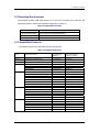
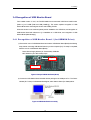
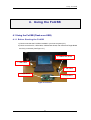
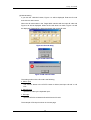
1
REJ10J0143-0401Z
USB Flash Writer
User's Manual
RENESAS SINGLE-CHIP MICROCOMPUTER
M16C FAMILY / 740 FAMILY
Rev.4.01
Revision date: Dec 24, 2004
Renesas Solutions Corp.
www.renesas.com
Keep safety first in your circuit designs!
1. Renesas Technology Corporation puts the maximum effort into making semiconductor products
better and more reliable, but there is always the possibility that trouble may occur with them. Trouble
with semiconductors may lead to personal injury, fire or property damage.
Remember to give due consideration to safety when making your circuit designs, with appropriate
measures such as (i) placement of substitutive, auxiliary circuits, (ii) use of nonflammable material or
(iii) prevention against any malfunction or mishap.
Notes regarding these materials
1. These materials are intended as a reference to assist our customers in the selection of the Renesas
Technology Corporation product best suited to the customer's application; they do not convey any
license under any intellectual property rights, or any other rights, belonging to Renesas Technology
Corporation or a third party.
2. Renesas Technology Corporation assumes no responsibility for any damage, or infringement of any
third-party's rights, originating in the use of any product data, diagrams, charts, programs,
algorithms, or circuit application examples contained in these materials.
3. All information contained in these materials, including product data, diagrams, charts, programs and
algorithms represents information on products at the time of publication of these materials, and are
subject to change by Renesas Technology Corporation without notice due to product improvements
or other reasons. It is therefore recommended that customers contact Renesas Technology
Corporation or an authorized Renesas Technology Corporation product distributor for the latest
product information before purchasing a product listed herein.
The information described here may contain technical inaccuracies or typographical errors.
Renesas Technology Corporation assumes no responsibility for any damage, liability, or other loss
rising from these inaccuracies or errors.
Please also pay attention to information published by Renesas Technology Corporation by various
means, including the Renesas Technology Corporation Semiconductor home page
(http://www.renesas.com).
4. When using any or all of the information contained in these materials, including product data,
diagrams, charts, programs, and algorithms, please be sure to evaluate all information as a total
system before making a final decision on the applicability of the information and products. Renesas
Technology Corporation assumes no responsibility for any damage, liability or other loss resulting
from the information contained herein.
5. Renesas Technology Corporation semiconductors are not designed or manufactured for use in a
device or system that is used under circumstances in which human life is potentially at stake.
Please contact Renesas Technology Corporation or an authorized Renesas Technology Corporation
product distributor when considering the use of a product contained herein for any specific
purposes, such as apparatus or systems for transportation, vehicular, medical, aerospace, nuclear,
or undersea repeater use.
6. The prior written approval of Renesas Technology Corporation is necessary to reprint or reproduce
in whole or in part these materials.
7. If these products or technologies are subject to the Japanese export control restrictions, they must
be exported under a license from the Japanese government and cannot be imported into a country
other than the approved destination.
Any diversion or reexport contrary to the export control laws and regulations of Japan and/or the
country of destination is prohibited.
8. Please contact Renesas Technology Corporation for further details on these materials or the
products contained therein.
Microsoft, MS, and MS-DOS are registered trademarks of Microsoft Corporation of the U.S.
Windows is trademark of Microsoft Corporation of the U.S.
IBM and PC/AT are registered trademarks of International Business Machines Corporation of the U.S.
Pentium is a trademark of Intel Corporation of the U.S.
Adobe and Acrobat are registered trademarks of Adobe Systems Incorporated.
Preface
Thank you for purchasing Renesas USB Flash Writer (M3A-0665).
This manual describes how to use the hardware and software products included with USB Flash Writer
(M3A-0665). To other tools, look other tools's manulas.
Table of Content
Table of Content
1.
Contents of Product ......................................................................................................................................... 4
1.1 Contents of product ........................................................................................................................................ 4
1.2 Operating Environment .................................................................................................................................. 5
1.3 Compatible Products...................................................................................................................................... 5
1.4 Board Specification......................................................................................................................................... 7
1.5 CD-ROM......................................................................................................................................................... 8
1.6 System Requirements.................................................................................................................................... 8
2.
Product Specifications...................................................................................................................................... 9
2.1 FoUSB (Flash-over-USB) .............................................................................................................................. 9
2.2 KD30/KD3083 ................................................................................................................................................ 9
3.
Installing..........................................................................................................................................................11
3.1 Before installing ............................................................................................................................................11
3.2 Preparation before installing.........................................................................................................................11
3.3 FoUSB (Flash-over-USB) installing .............................................................................................................12
3.3.1 Method of Installation............................................................................................................................12
3.3.2 Method of Uninstallation .......................................................................................................................17
3.4 Recognition of USB Monitor Board..............................................................................................................18
3.4.1 Recognition of USB Monitor Board 1 (for USBMON Driver) ...............................................................18
3.4.2 Recognition of USB Monitor Board 2 (for FoUSB Driver)....................................................................20
3.4.3 Other Notes...........................................................................................................................................23
3.5 KD30/KD3083 intalling .................................................................................................................................24
3.5.1 Installing.................................................................................................................................................24
3.5.2 Uninstalling the Remote Debugger ......................................................................................................26
4.
Using the FoUSB ...........................................................................................................................................27
4.1 Using the FoUSB (Flash-over-USB)............................................................................................................27
4.1.1 Before Starting the FoUSB ...................................................................................................................27
4.1.2 FoUSB starts.........................................................................................................................................30
4.1.3 Details of Main Button 1........................................................................................................................31
4.1.4 Details of the Update Button.................................................................................................................42
4.1.5 Details of the Select MCU Button .........................................................................................................43
4.1.6 Monitor Information ...............................................................................................................................47
4.1.7 Detailed File Information .......................................................................................................................47
4.1.8 Details of Main Button 2........................................................................................................................47
i
Table of Content
4.2.Other Functions ............................................................................................................................................48
5.
Using the KD ..................................................................................................................................................49
5.1 Using the KD.................................................................................................................................................49
5.1.1 Before Starting the KD..........................................................................................................................49
5.1.2 Starting the KD......................................................................................................................................50
5.1.3 Program Download ...............................................................................................................................55
5.1.4 Program Execution ...............................................................................................................................56
5.1.5 Program Stop........................................................................................................................................56
5.1.6 Program Step Execution.......................................................................................................................56
5.1.7 Software Break Method ........................................................................................................................57
5.1.8 Reset Execution....................................................................................................................................57
5.1.9 KD Completion......................................................................................................................................57
5.1.10 If a Communication Error Occurs .......................................................................................................58
5.1.11 Error Except a Communication Error Occurs.....................................................................................58
5.1.12 Operation Method ...............................................................................................................................58
5.2 KD Limitations...............................................................................................................................................59
5.2.1 Limitations on Special Page Vector......................................................................................................59
5.2.2 A limitation item about the C language.................................................................................................60
5.2.3 Limitations on Memory Extension.........................................................................................................61
5.2.4 Precautions on Internal Reserved Area Expansion Bit........................................................................61
5.2.5 Limitations on Stop and Wait Modes....................................................................................................62
5.2.6 Realtime Capability of the User Program.............................................................................................62
5.3 Memory Map Limitations..............................................................................................................................63
5.4 Peripheral Function Related Limitations ......................................................................................................66
5.5 FoUSB Debugger Principle..........................................................................................................................66
5.5.1 Communication Function with FoUSB .................................................................................................67
5.5.2 Command Execution ............................................................................................................................67
5.5.3 The difference from an actual CPU operation......................................................................................68
6.
Troubleshooting..............................................................................................................................................69
6.1 FoUSB cannot communicate with the Target MCU Why?..........................................................................69
6.2 The MCU cannot enter standerd serial I/O why? ........................................................................................69
6.3 The MCU cannot be programmed using FoUSB Why? .............................................................................69
6.4 FoUSB cannot operate Why? ......................................................................................................................69
6.4.1 Compulsive download procedure of firmware......................................................................................71
6.5 Can FoUSB information be transmitted to KD?...........................................................................................74
6.6 A communication error occurs when the KD starts. What is the cause of this problem?...........................74
ii
Table of Content
6.7 A communication error occurred when debugging the program. What is the cause of this problem? ......74
6.8 A message "Source file cannot be found" was output. What should I do?.................................................75
6.9 Is peripheral I/O operating during a break? .................................................................................................75
6.10 Can coveragefunction be used in KD?......................................................................................................75
6.11 Can check sum function be used?.............................................................................................................75
6.12 ID code written to microcomputer after KD exits? .....................................................................................75
6.13 Debug operation has not worked well........................................................................................................76
6.14 Message List ..............................................................................................................................................78
7.
Appendix.........................................................................................................................................................79
7.1 USB Monitor Board ......................................................................................................................................79
7.1.1 Board Specifications .............................................................................................................................79
7.1.2 Pin Assignments ...................................................................................................................................80
7.1.3 Example Connection.............................................................................................................................80
7.1.4 Power Source Supply Selector.............................................................................................................87
7.1.5 LED Status Indicators ...........................................................................................................................87
7.2 Installation of a USB Driver, and recognition of USB Monitor Board (Manual setup).................................88
7.2.1 For USBMON Driver.............................................................................................................................88
7.2.2 For FoUSB Driver .................................................................................................................................91
7.3 Referencing Electronic Manuals ..................................................................................................................95
7.4 Product Information ......................................................................................................................................95
iii
1 Contents of Product
1. Contents of Product
This section shows the contents of theUSB Flash Writer’s product package. When
unpacking your USB Flash Writer, check to see that all products listed below are included.
1.1 Contents of product
Table 1-1 lists the products included in the USB Flash Writer.
Table 1-1 USB Flash Writer Product List
Product List
Quantity
Remark
USB Monitor Board
1pc
USB Cable (Used for the connection with the Host Computer.)
1pc
Flat Cable
1pc
Pin Header (HIF3FC-10P-2.54DSA: straight type)
1pc
Note 1
CD-ROM
1pc
Note 2
Note 1: Starter kit doesn't include pin header (straight type).
Note 2: When a FoUSB is included with starter kit, only one CD-ROM is in the FoUSB.
4
1 Contents of Product
1.2 Operating Environment
The software includes USB Flash Writer run on the Host Computer (PC) under the OS
(Operating System) version that are listed respectively in Table 1-2.
Table 1-2 Operating Environment
Host Computer (PC)
IBM PC/AT series or its compatible
OS (Operating System)
Microsoft Windows 98SE/ME/2000/XP
CPU
Pentium II 233MHz or newer recommended
Memory
8 Mbyte or more (16 Mbyte recommended)
1.3 Compatible Products
Compatible products with USB Flash Writer are as follows.
Table 1-3 Compatible Products (1)
Group
MCU Product Name
Corresponding
MCU Product Name
Software
to select in Software
FoUSB, KD30
M30102F3
M16C/10
M30100F3FP, M30102F3FP
M16C/1N
M301N2F8TFP
FoUSB, KD30
M301N2F8
M16C/24
M30245FCGP
FoUSB, KD30
M30245FC
M16C/26
M30262F3GP
FoUSB, KD30
M30262F3
M30262F4GP
FoUSB, KD30
M30262F4
M30262F6GP
FoUSB, KD30
M30262F6
M30262F8GP
FoUSB, KD30
M30262F8
M30260F3AGP
FoUSB, KD30
M30260F3A
M30260F4AGP
FoUSB, KD30
M30260F4A
M30260F6AGP
FoUSB, KD30
M30260F6A
M30260F8AGP
FoUSB, KD30
M30260F8A
M30263F3AFP
FoUSB, KD30
M30263F3A
M30263F4AFP
FoUSB, KD30
M30263F4A
M30263F6AFP
FoUSB, KD30
M30263F6A
M30263F8AFP
FoUSB, KD30
M30263F8A
M30280F6HP
FoUSB, KD30
M30280F6
M30280F8HP
FoUSB, KD30
M30280F8
M16C/26A
M16C/28
M16C/29
M30280FAHP
FoUSB, KD30
M30280FA
M30281F6HP
FoUSB, KD30
M30281F6
M30281F8HP
FoUSB, KD30
M30281F8
M30281FAHP
FoUSB, KD30
M30281FA
M30290F8HP
FoUSB, KD30
M30290F8
M30290FAHP
FoUSB, KD30
M30290FA
M30290FCHP
FoUSB, KD30
M30290FC
M30291F8HP
FoUSB, KD30
M30291F8
M30291FAHP
FoUSB, KD30
M30291FA
M30291FCHP
FoUSB, KD30
M30291FC
5
1 Contents of Product
Table 1-4 Compatible Products (2)
Group
MCU Product Name
Corresponding
MCU Product Name
Software
to select in Software
M16C/24
M30245FCGP
FoUSB, KD30
M30245FC
M16C/62A(M)
M30620FCAFP/GP, M30621FCAGP
FoUSB, KD30
M30620FCA
FoUSB, KD30
M30624FGA
M30622F8PFP/GP
FoUSB, KD30
M30622F8P
M30623F8PGP
FoUSB, KD30
M30623F8P
M30620FCPFP/GP
FoUSB, KD30
M30620FCP
M30621FCPGP
FoUSB, KD30
M30621FCP
M30624FGPFP/GP
FoUSB, KD30
M30624FGP
M30625FGPGP
FoUSB, KD30
M30625FGP
M30626FHPFP/GP
FoUSB, KD30
M30626FHP
M30627FHPGP
FoUSB, KD30
M30627FHP
M30626FJPFP/GP
FoUSB, KD30
M30626FJP
M30627FJPGP
FoUSB, KD30
M30627FJP
M16C/62N
M3062GF8NFP/GP
FoUSB, KD30
M3062GF8
M16C/6N
M306N4FCTFP
FoUSB, KD30
M306N4FC
M306N4FGTFP
FoUSB, KD30
M306N4FG
M306N5FCTFP
FoUSB, KD30
M306N5FC
M306NAFGTFP
FoUSB, KD30
M306NAFG
M306NBFCTFP
FoUSB, KD30
M306NBFC
M16C/80
M30800FCFP/GP, M30802FCGP
FoUSB, KD3083
M30800FC
M30803FGFP/GP, M30805FGGP
FoUSB, KD3083
M30803FG
M32C/83
M30833FJFP/GP
FoUSB, KD3083
M30833FJ
M30835FJGP
FoUSB, KD3083
M30835FJ
M32C/84
M30843FJFP/GP, M30845FJGP
FoUSB, KD3083
M30845FJ
M32C/85
M30853FHFP/GP, M30855FHGP
FoUSB, KD3083
M30855FH
M30853FWFP/GP, M30855FWGP
FoUSB, KD3083
M30855FW
M30850FJFP/GP, M30852FJGP
FoUSB, KD3083
M30852FJ
M32C/86
M30865FJGP
FoUSB, KD3083
M30865FJ
M32C/87
M30879FLFP/GP, M3087BFLGP
FoUSB, KD3083
M3087BFL
R8C/10
R5F21102FP
FoUSB, KD30
R5F21102 (R5F21104 *1)
R5F21103FP
FoUSB, KD30
R5F21103 (R5F21104 *1)
R5F21104FP
FoUSB, KD30
R5F21104
R5F21112FP
FoUSB, KD30
R5F21112 (R5F21114 *1)
R5F21113FP
FoUSB, KD30
R5F21113 (R5F21114 *1)
R5F21114FP
FoUSB, KD30
R5F21114
R5F21122FP
FoUSB, KD30
R5F21122 (R5F21124 *1)
R5F21123FP
FoUSB, KD30
R5F21123 (R5F21124 *1)
R5F21124FP
FoUSB, KD30
R5F21124
R5F21132FP
FoUSB, KD30
R5F21132 (R5F21134 *1)
R5F21133FP
FoUSB, KD30
R5F21133 (R5F21134 *1)
R5F21134FP
FoUSB, KD30
R5F21134
M30620FCMFP/GP, M30621FCMGP
M30624FGAFP/GP, M30625FGAGP
M30624FGMFP/GP, M30625FGMGP
M16C/62P
R8C/11
R8C/12
R8C/13
7542
M37542F8SP/FP/GP
FoUSB
M37542F8
38C2
M38C29FFAFP/HP
FoUSB
M38C29FF
*1: When using the KD30.
6
1 Contents of Product
1.4 Board Specification
Table 1-5 shows the USB Monitor Board Specification. When saving these products, put
them into the conductive bag. Store them into the container box which is used for shipping
as possible
Table 1-5 USB Monitor Board Specification
Item
Debug formula
Monitor program
USB microcomputer
USB interface (J1)
Target interface (J3)
Operation voltage
Power consumption
Board size
Use environment condition
(at the time of operation)
Use environment condition
(at the time of storage)
Description
Monitor program formula
ROM size: Approx. 1600 byte
* In the case of R8C/Tiny Series, 2K byte
RAM size: 128 byte
* In the case of M16C/80 Group, 256 byte
* In the case of M32C/80 Series, 256 byte
* In the case of R8C/Tiny Series, not used
Operation frequency: 700KHz or above (Note1)
Operation mode: Single chip mode
Software break: 2 points to 8 points (Note2)
M37641F8HP (8 bit USB flash microcomputer)
USB2.0 full speed
Synchronous serial Interface
Starter kit and 10 pin connector for target board connection
4.75V to 5.25V
(USB bus-powered supply or target supply enabled)
3.0V to 3.6V (supply from target is necessary) (Note3)
Max.50mA
70mm x 29mm
Temperature: 25±5°C (no corrosive gas)
Humidity: no condensation
Temperature: 25±5°C (no corrosive gas)
Humidity: no condensation
Note 1: Maximum operating frequency is dependent on the MCU.
Note 2: Software break numbers are dependent on the address match circuit numbers
are built-in MCU.
Note 3: When operating in 3.3V, supply power from the target board. In this case, it is not
possible to change the FoUSB firmware. When the model name of the
microcomputer to be used is changed, remove the target board, supply the USB
bus-powered and rewrite the firmware.
7
1 Contents of Product
1.5 CD-ROM
The CD-ROM contains software products necessary for developing programs and
electronic manuals as well. Here follow the contents of the CD-ROM.
CD-ROM: Rev.2.10 or later
\root
|--- Readme_e.txt
|--- Readme_j.txt
|--- \Document
|--- \FOUSB
|
|--- \USB Drivers
|
|--- \KD
|
|--- \KD30
|
|--- \KD3083
|
|--- \NC
|--- \NC30WA
|--- \NC308WA
: Readme File (English version)
: Readme FIle (Japanese version)
: User’s manual is included (English and Japanease version)
: FoUSB Installer is included (English and Japanese common version)
: USB Driver is included (English and Japanese common version)
: KD30 Installer is included (English and Japanese version)
: KD3083 Installer is included (English and Japanses version)
: NC30WA C Compiler is included (English and Japanese version) Note
: NC308WA C Compiler is included (English and Japanese version) Note
Note: Entry version
1.6 System Requirements
In addition to the products listed above, you must have the following equipment before
you can use the USB Flash Writer.
1) Host Computer (PC)
2) Target Board
8
2 Product Specifications
2. Product Specifications
2.1 FoUSB (Flash-over-USB)
FoUSB is the software that allows you to operate on M16C, M32C, R8C or 740
microcomputers with built-in flash memory from a Windows version host computer
(Windows 98SE or later).
2.2 KD30/KD3083
The KD included with the package is the debug software that runs on a Windows version
host computer. This KD is usable for only the R8C/Tiny, M16C/10, M16C/20, M16C/Tiny,
M16C/60, M16C/80 or M32C/80 series of Renesas 16-bit and 32-bit single-chip
microcomputers with built-in flash memory. The KD provides a powerful debugging
environment. In addition, it is operationally compatible with and can therefore be used the
same way as PD30 (or PD308F), the emulator control debugger for Renesas 16C/62
microcomputers. The features of the Remote Debugger are outlined below. For details,
see Section “5. Using the KD”.
Table 2-1 PD30 and KD30 comparison
No.
Item
PD30
KD30
1
Software break function
64 points
2 points to 8 points (Note)
2
Hardware break function
6 points
not included
3
RAM monitor function
included
included
4
Real time trace
included
not included
5
Time measurement function
included
not included
6
Script function
included
included
Note: Software break numbers are dependent on the address match circuit numbers are
built-in MCU.
9
2 Product Specifications
Table 2-2 PD308F and KD3083 comparison
No.
Item
PD308F
KD3083
1
Software break function
64 points
4 points to 8 points (Note)
2
Hardware break function
6 points
not included
3
RAM monitor function
included
included
4
Real time trace
included
not included
5
Time measurement function
included
not included
6
Script function
included
included
Note: Software break numbers are dependent on the address match circuit numbers are
built-in MCU.
NOTICE: The software break number of MCUs
Group
software break
number
M16C/10
2 points
M16C/1N
M16C/24
M16C/26, 26A
M16C/28
M16C/29
M16C/62A(M)
M16C/62P
M16C/62N
2 points
2 points
6 points
6 points
6 points
2 points
8 points
2 points
Group
software break
number
M16C/6N
(M3062NAFG, M3062NBFC)
2 points
M16C/6N
(M306N4FC, M306N4FG,
M306N5FC)
8 points
R8C/Tiny Series
M16C/80
M32C/83
M32C/84, 85, 86, 87
2 points
4 points
4 points
8 points
10
3 Installing
3. Installing
3.1 Before installing
Do not connect the USB Cable which belongs to this product to the Host computer (PC) before
installing.
3.2 Preparation before installing
Be sure to confirm the following point before performing installation of a tool (GUI) and a driver.
(1) The CD-ROM includes files required for the FoUSB (Flash-over-USB) installation. Copy all files
to any folder in your PC before installation.
(2) All tools and USB drivers must be installed with the administrator if installed on Windows
2000/XP. Both PowerUser (for a standard access) and User (for a limited access) can use
software after installation.
11
3 Installing
3.3 FoUSB (Flash-over-USB) installing
3.3.1 Method of Installation
1) To install FoUSB, double-click “FoUSB_V.*.**.exe” on the folder into which you’ve copied FoUSB
files from the CD-ROM.
2) Select the language of installer.
3) Click the <Next> button.
4) Only when you agree, click the <I Agree> button.
12
3 Installing
5) Choose the component which you want to install and click the <Next> button.
NOTICE: Explanation of install component
(a) Shortcut on Desktop
The shortcut of a FoUSB (Flash-over-USB) execution file is created on a desktop.
(b) Install USB Drivers
FoUSB installer installs a USB Driver in the correct location of Windows system automatically.
We recommend choosing this component in all operating systems. In addition, when this
component is not chosen, please perform installation of a USB Driver, and recognition of USB
Monitor Board with reference to [7.2 Installation of a USB Driver, and recognition of USB Monitor
Board (Manual setup)].
(c) Update KD30 Files
FoUSB installer updates KD30 to KD30 with a firmware older than the firmware of FoUSB.
(d) Update KD3083 Files
FoUSB installer updates KD3083 to KD3083 with a firmware oloder than the firmware of
FoUSB.
13
3 Installing
6) Choose the install location of FoUSB and click the <Install> button. The default install location of
FoUSB is “C:\MTOOL\FOUSB”.
7) The following figure is displayed when the install component “Install USB Drivers” is choosen.
Click the <Yes> button.
Next, warning is displayed. Please check that USB Monitor Board is not connected to your host
computer (PC), and click the <OK> button.
14
3 Installing
8) When an operating system is Windows XP, notes screen is displayed. Click the <OK> button.
Then the software install screen is displayed two times (for USBMON Driver and FoUSB Driver),
click the <Continue Anyway> button twice (Note).
Note: Microsoft has advocated authentication of the USB drivers to the USB vendors in the
Microsoft® Windows® XP and Windows®-based operating systems released after Microsoft®
Windows® XP. This is aimed at elimination of illegal drivers and improvement of host computer
(PC). Renesas USB Drivers are not authenticated by Microsoft, but we provide them based on
the sufficient examination.
9) The following figure is displayed when the USB Driver is already installed in the PC. Click the
<OK> button.
USBMON Driver
FoUSB Driver
15
3 Installing
10) The following figure is displayed when installation of USB Driver is completed. Click the <OK>
button.
11) When the install component “Update KD30 Files” is chosen, FoUSB installer seaches KD30
with a firmware older than the firmware of FoUSB. The following figure will be displayed if KD30
is detected.
If you want to update a firmware, click the <Yes> button. When <No> button is clicked, the
firmware of KD30 is not updated.
Note: When the install component “Update KD3083 Files” is chosen, the update check screen is
displayed like the above.
16
3 Installing
12) Finally, click the <Finish> button.
13) Now you’ve finished installing the FoUSB (Flash-over-USB).
3.3.2 Method of Uninstallation
To uninstall the FoUSB (Flash-over-USB) you've installed, choose Settings -- Control Panel from the
Start menu, and then click “Add/Remove Programs”. Select "Flash-over-USB V.*.** " from the
program list and click the <Add/Remove> button. An uninstall window will appear, with the
Flash-over-USB V.*.** compiler uninsalled.
17
3 Installing
3.4 Recognition of USB Monitor Board
From installer version “V.2.04”, the FoUSB installer has an automatic USB Driver install function
(Refer to [3.3 FoUSB (Flash-over-USB) installing].). This section explains recognition of USB
Monitor Board when confirming this function and installing FoUSB.
When this function is not confirmed, please perform installation of a USB Driver, and recognition of
USB Monitor Board with reference to [7.2 Installation of a USB Driver, and recognition of USB
Monitor Board (Manual setup)].
3.4.1 Recognition of USB Monitor Board 1 (for USBMON Driver)
1) Remove the cover of USB Monitor Board and make a USB Monitor Board (Board) the following
setup, before connecting USB Monitor Board to your host computer (PC). If a setup is completed,
attach a cover in a USB Monitor Board (Board).
Power Source Supply Selector (S1: Power Mode): USB side
MCU Mode Pin (JP1: MCU Mode): Open
Open
USB side
Figure 3-1 Setup of USB Monitor Board (Board)
2) Connect the USB Monitor Board included with the package to the USB port of PC. The Power
indicator (D1: Power) of USB Monitor Board lights, and a Status indicator (D4: Status) blinks.
Figure 3-2 USB Monitor Board connectivity
18
3 Installing
3) When an operating system is WIndows 98SE/ME/2000, Windows system detect USB Driver
automatically and recognizes USB Monitor Board. Recognition of USB Monitor Board for
USBMON Driver is completion.
4) When an operating system is Windows XP, Windows system displays the Found New
Hardware Wizard screen. Then, choose “Install the software automatically” and click the <Next>
button.
5) Next, the Hardware Installation screen is displayed, click the <Continue Anyway> button (Note).
Note: Microsoft has advocated authentication of the USB drivers to the USB vendors in the
Microsoft® Windows® XP and Windows®-based operating systems released after Microsoft®
Windows® XP. This is aimed at elimination of illegal drivers and improvement of host computer
(PC). Renesas USB Drivers are not authenticated by Microsoft, but we provide them based on
the sufficient examination.
19
3 Installing
6) Click the <Finish> button. Windows system recognizes USB Monitor Board (for USBMON
Driver).
Recognition of USB Monitor Board for USBMON Driver is completion.
3.4.2 Recognition of USB Monitor Board 2 (for FoUSB Driver)
1) Remove the cover of USB Monitor Board and make a USB Monitor Board (Board) the following
setup, before connecting USB Monitor Board to your host computer (PC). If a setup is completed,
attach a cover in a USB Monitor Board (Board).
Power Source Supply Selector (S1: Power Mode): USB side
MCU Mode Pin (JP1: MCU Mode): Shorted
Shorted
USB side
Figure 3-3 Setup of USB Monitor Board (Board)
20
3 Installing
2) Connect the USB Monitor Board included with the package to the USB port of PC. The Power
indicator (D1: Power) of USB Monitor Board lights.
Figure 3-4 USB Monitor Board connectivity
3) When an operating system is WIndows 98SE/ME/2000, Windows system detect USB Driver
automatically and recognizes USB Monitor Board. Recognition of USB Monitor Board for
USBMON Driver is completion.
Please skip to 7).
4) When an operating system is Windows XP, Windows system displays the Found New
Hardware Wizard screen. Then, choose “Install the software automatically” and click the <Next>
button.
21
3 Installing
5) Next, the Hardware Installation screen is displayed, click the <Continue Anyway> button (Note).
Note: Microsoft has advocated authentication of the USB drivers to the USB vendors in the
Microsoft® Windows® XP and Windows®-based operating systems released after Microsoft®
Windows® XP. This is aimed at elimination of illegal drivers and improvement of host computer
(PC). Renesas USB Drivers are not authenticated by Microsoft, but we provide them baased
on the sufficient examination.
6) Click the <Finish> button. Windows system recognizes USB Monitor Board (for FoUSB Driver).
Recognition of USB Monitor Board for FoUSB Driver is completion.
7) Separate USB Monitor Board from host computer (PC).
8) Finally remove the cover of USB Monitor Board and set the MCU Mode Pin (JP1: MCU Mode)
as “Open”.
22
3 Installing
3.4.3 Other Notes
Caution: The “USB Drivers” folder below is stored.
Driver Name
USBMON Driver
Description
Related Files
USBMON driver is a driver for using usbmon.sys
FoUSB (Flash-over-USB) and KD (KD30,
usbmon.inf
KD3083)
FoUSB Driver
FoUSB driver is a driver for using USB fousb.sys
MCU (M367641F8) of USB Monitor fousb.inf
Board in Boot mode. (Note)
(Note)
The Boot mode of USB MCU is used only for the use shown below.
1) Installation of FoUSB Driver
2) When the firmware of USB MCU is erased or damaged
When the firmware of USB MCU is erased or damaged, the phenomenon of [6.4 FoUSB cannot
operate Why?] or [6.6 A communication error occurs when the KD starts. What is the cause of
this problem?] occurs.
In this case, it is necessary to install FoUSB driver (first time only) and download firmware
compulsorily on a USB MCU. Please refer to [6.4 FoUSB cannot operate Why?].
23
3 Installing
3.5 KD30/KD3083 intalling
3.5.1 Installing
1) Installing the Remote Debugger
Double-click installer file on the CD-ROM (\KD\KD30) for KD30.
In KD3083, the installer file is included in \KD\KD3083.
2) A flow of installation procedures is shown in the pages that follow.
(a) Click the <Yes> button.
(b) Click the <Next> button.
(c) Only when you agree, click the <Yes> button
24
3 Installing
(d) Click the <Next> button.
A default install location is “C:\MTOOL”. If an install location is changed, please click the
<Browse> button and determine an install location.
(e) Click the <Yes> button.
(f) Click the <OK> button.
3) Now you've finished installing the KD30.
Note: The installation of KD3083 is the same.
25
3 Installing
3.5.2 Uninstalling the Remote Debugger
To uninstall, choose Settings -- Control Panel from the Start menu, and then click the
“Add/Remove Programs”. Select KD from the program list and click the <Add/Remove> button.
An uninstall window will appear, with the integrated development environment uninsalled.
The uninstallation of KD3083 is the same, too.
26
4 Using the FoUSB
4. Using the FoUSB
4.1 Using the FoUSB (Flash-over-USB)
4.1.1 Before Starting the FoUSB
1) Check to see that the FoUSB is installed in your host computer (PC).
2) Check to see that PC, USB Cable, USB Monitor Board, Flat Cable and Target Board
are firmly connected. (See Figure 4-1)
3. USB Monitor Board
1. USB Cable
4. Flat Cable
2. Target Board
5. Target MCU
Figure 4-1 connect-1
27
4 Using the FoUSB
3) Connection Method
It specifies as a premise that MCU is carried on the Target Board.
(1) Connection order when using the USB bus-powered.
Connect in order of 2-4-3-1-host computer (PC).
(2) Separation order after using the USB bus-powered.
Connect in order of PC-1-3-4-2.
(3) Connection order when using external power supply.
Set a power source supply selector to the TARGET side.
Connect in order of PC-1-3-4-2 and finally supply power from outside.
(4) Separation order after using external power supply.
Drop the power which is supplied from outside.
Separate in order of PC-1-3-4-2.
4) The power source supply selector on the USB Monitor Board must be set differently
depending on the Target MCU used.
(1) When using 5 V
The power for the Target MCU is supplied from the USB Monitor Board.
Therefore, there is no need to supply power for the Target MCU from the Target
Board. In this case, set the power supply selector on the USB Monitor Board to
the USB side as shown in Figure 4-2.
When using 5 V, set the
switch to the USB side.
Figure 4-2 Power source supply selector-1
28
4 Using the FoUSB
(2) When using 3.3 V
The power for the Target MCU is not supplied from the USB Monitor Board and
must therefore be supplied from the Target Board. In this case, set the power
source supply selector on the USB Monitor Board to the TARGET side as shown in
Figure 4-3.
When using 3.3 V, set the
switch to the TARGET side.
Figure 4-3 Power source supply selector-2
(3) Other
Depending on the host computer (PC) environment you are using, no 5 V power
supply may be fed to the Target MCU even when the select switch on the USB
Monitor Board is set to the USB side. In such a case, set the power source supply
selector to the TARGET side so that the power for the Target MCU will be supplied
from the Target Board.
29
4 Using the FoUSB
4.1.2 FoUSB starts
1) From the Start menu, choose Programs -- RENESAS-TOOLS – Flash-over-USB
V.*.** -- FoUSB Programmer to start the FoUSB. When the FoUSB starts, the
FoUSB main window shown in Figure 4-4 appears.
i) Main button 1
iii) MCU select button
iv) Monitor information
v) Detail button
ii) Update button
vi) Main button 2
Figure 4-4 FoUSB main window
2) Guide to understanding the display of the main screen
No.
Item
i
Main button 1
ii
iii
iv
v
vi
Update button
MCU select button
Monitor information
Detail button
Main button 2
Content
Use these main buttons to download a program as well as
read, erase or write to the flash memory.
Click this button to upgrade the FoUSB version.
Use this button to select the Target MCU.
Shows information on the selected MCU.
Shows detailed information on the downloaded program.
Use these main buttons to set functions, show help or exit.
30
4 Using the FoUSB
4.1.3 Details of Main Button 1
1) “OPEN” button
This button reads the downloading (programming) file to the Target MCU.
(1) Click the “OPEN” button, and the screen shown in Figure 4-5 will appear, allowing
you to choose the file to download into the Target MCU. The type of file that can be
downloaded is HEX or Motorola. After selecting the file to download, click the
<Open> button.
Figure 4-5 Open screen
(2) The ID code is automatically read in. Click the <OK> button.
If file don’t have ID code, a message is not displayed.
Figure 4-6 ID code screen
Note: A file which is out of flash area cannot be open.
31
4 Using the FoUSB
2) “READ” button
This button performs to verify data written in the Target MCU and the file read by
“OPEN”. Also, performs to read out data written in the Target MCU.
(1) Clik the “READ” button, Figure 4-7 screen will appear.
Figure 4-7 Flash Memory Read screen-1
(2) For Verify, click the <verify> button and the file downloaded by “OPEN” and data
written in the Target MCU will be verified. If the verified result matches, Figure 4-8
will appear. Click the <OK> button.
Figure 4-8 Verify OK screen
If the data does not match, following figure will be displayed.
32
4 Using the FoUSB
(3) For “Read Area”, specify the range of data to read in hexadecimal. By default, the
data opens in a custom window. Click the <Read Area> button, and the
downloaded data will be displayed, but not saved. If you wish, select the <Show
ASCII> check box in the Options section, and ASCII code will be added to the
downloaded data. (See Figure 4-9 and Figure 4-10)
Figure 4-9 Flash Memory Read screen-2
Figure 4-10 Flash Memory Contents
33
4 Using the FoUSB
(4) To change the custom window used for displaying data to an editor, select the
<Display using>. By default, data is displayed in Notepad. To change Notepad to
any editor, click the <Change Editor> button. (See Figure 4-11)
Figure 4-11 Flash Memory Read screen-3
(5) To save the read data, select the <Save to Motorola S-Record File> and click the
<Read Area> button. (See Figure 4-12)
Then enter a name for the file. (See Figure 4-13)
Figure 4-12 Flash Memory Read screen-4
34
4 Using the FoUSB
Figure 4-13 Save screen
3) “ERASE” button
This button erases the Flash ROM in the Target MCU.
(1) When you click the “ERASE” button, the screen changes to one of the following
two depending on whether you’ve downloaded data using “OPEN”.
(2) Before downloading
You can choose to erase all blocks (Select All) or erase evry one block. When you
select a block to erase, the check box by block is indicated with a check mark and
the block is displayed in color. Click the <Erase> button, and the block will be
erased. (See Figure 4-14)
Figure 4-14 Erase Flash-1
35
4 Using the FoUSB
(3) After downloading
The system reads information from the downloaded data to determine which block
to erase and marks the corresponding check box with a check mark and displays
the block in color. Click the <Erase> button, and the block will be erased. You can
erase all blocks collectively or one block at a time. (See Figure 4-15)
Figure 4-15 Erase Flash-2
4) “UNLOCK” button
This button sends the ID code to the locked Target MCU, and unlock the Target MCU.
In the “Locked” display as shown in the following figure, a flash command (program,
erase, read, verify) to the Target MCU cannot be executed.
Flash command can be executed.
Flash command
cannot be executed.
36
4 Using the FoUSB
When you click the “UNLOCK” button, the system checks ID code. The ID code check
has automatic setting and manual setting.
(1) Automatic setting
Automatic setting checks in the following condition in ID code of “All FFh” and “All
00h”.
>> When FoUSB is started.
>> When a firmware is changed during FoUSB use. This condition shows
FoUSB restart.
If the ID code consists “All 00h”, Figure 4-16 will be displayed, and the Target MCU
is unlocked. When the ID code of Target MCU is not “All FFh” or “All 00h”, please
unlock Target MCU using manual setting.
Figure 4-16 Unlocked screen
Automatic setting can select whether it performs by user. Click the “SETTING”
button and user setting screen is displayed. Select enabled or disabled in “Auto
Unlocok” check box and click the <Save> button.
Note: When the <Cancel> button is clicked on a user setting screen, a former setting
condition is saved.
37
4 Using the FoUSB
(2) Manual setting
If you click the “UNLOCK” button, Figure 4-17 will be displayed. Enter the ID code
and click the <OK> button.
When the ID code written in the Target MCU matches with the input ID code and
Figure 4-18 will be displayed. When the ID code does not match, Figure 4-19 will
be displayed (Target MCU is locked) and enter the correct ID code.
Figure 4-17 ID code dialog
Figure 4-18 ID code match
Figure 4-19 ID code not match
The setting method of the ID code is the following.
a. Macro input
The <Fill 00> button or the <Fill FF> button is clicked, and input “All 00h” or “All
FFh”.
b. Manual input
Input the ID code by the keyboard input.
c. File input
Input the HEX file or Motorola file which has an ID code.
The example of File input is shown in the next page.
38
4 Using the FoUSB
Example of File input
In this example, the ID code of “01 02 03 04 05 06 07” is programmed in the Target
MCU.
First, click the “OPEN” button and open the HEX file or Motorola file which has an
ID code. Click the <OK> button on the ID code screen which FoUSB displays. The
Motorola file with the ID code of “01 02 03 04 05 06 07” is open in this example.
Next, click the “UNLOCK” button. The screen into which the ID code of the read file
was input is displayed.
When clicking the “OK” button, the ID code written in the Target MCU and the input
ID code match and the Target MCU will be unlocked.
39
4 Using the FoUSB
NOTICE: ID code address of MCU
Series
M16C/10
M16C/20
M16C/Tiny
M16C/60
M16C/80
M32C/80
R8C/Tiny
740
38000
ID code address
ID1: 0FFFDFh
ID2: 0FFFE3h
ID3: 0FFFEBh
ID4: 0FFFEFh
ID5: 0FFFF3h
ID6: 0FFFF7h
ID7: 0FFFFBh
ID1: 0FFFFDFh
ID2: 0FFFFE3h
ID3: 0FFFFEBh
ID4: 0FFFFEFh
ID5: 0FFFFF3h
ID6: 0FFFFF7h
ID7: 0FFFFFBh
ID1: 0FFDFh
ID2: 0FFE3h
ID3: 0FFEBh
ID4: 0FFEFh
ID5: 0FFF3h
ID6: 0FFF7h
ID7: 0FFFBh
ID1: 0FFD4h
ID2: 0FFD5h
ID3: 0FFD6h
ID4: 0FFD7h
ID5: 0FFD8h
ID6: 0FFD9h
ID7: 0FFDAh
The ID code address of MCU and the ID code input forms of FoUSB are the
following relations.
40
4 Using the FoUSB
5) “PROGRAM” button
This button performs programming to the Target MCU.
(1) Click the “PROGRAM” button, and the screen shown in Figure 4-20 will appear.
Figure 4-20 Program Flash screen
(2) In the Choose an Options section, select either “Erase -> Program -> Verify” or
“Program Only”.
(a) Erase -> Program -> Verify (without lock bit function)
When you select this option, processing is performed in order of Erase, Program and
Verify. A progress bar is displayed, indicating the progress of processing in Erase,
Program and Verify.
(b) Program Only (without lock bit function)
When you select this option, processing is performed for only programming. A progress
bar is displayed, indicating the progress of processing in programming.
Note: The following warning will be displayed if clicking the “Program Only” before
erasing the Target MCU. Clik the <Yes> button, only when Target MCU is blank
chip.
If the Target MCU is not blank, erase Flash ROM of the Target MCU and
perform the program process.
41
4 Using the FoUSB
(3) Erasing Options is useful when you select “Erase -> Program -> Verify” for
Choose An Options, allowing you to select the method for erasing flash memory
blocks.
(a) Erase All Blocks
All flash blocks are erased
(b) Erase Only Needed Block
Only the corresponding flash block is erased.
4.1.4 Details of the Update Button
Use the “Update” button when you want to upgrade the version of FoUSB.
42
4 Using the FoUSB
4.1.5 Details of the Select MCU Button
1) The following MCUs can be selected in FoUSB.
Group
MCU Product Name
to select in FoUSB
Group
MCU Product Name
to select in FoUSB
Group
MCU Product Name
to select in FoUSB
M16C/10
M16C/1N
M16C/24
M16C/26
M30102F3
M301N2F8
M30245FC
M30262F3
M30262F4
M30262F6
M30262F8
M16C/62A
(62M)
M30620FCA
M30624FGA
M3062GF8N (Note)
R8C/10
R5F21102
R5F21103
R5F21104
M16C/62P
M30622F8P
M30623F8P
M30620FCP
M30621FCP
M30624FGP
M30625FGP
M30626FHP
M30627FHP
M30626FJP
M30627FJP
R8C/11
R5F21112
R5F21113
R5F21114
R5F21122
R5F21123
R5F21124
7542
R5F21132
R5F21133
R5F21134
M37542F8
M16C/6N
M306N4FC
M306N4FG
M306N5FC
M306NAFG
M306NBFC
38C2
M38C29FF
M16C/80
M30800FC
M30803FG
M32C/83
M30833FJ
M30835FJ
M30845FJ
M30855FH
M30855FW
M30852FJ
M30865FJ
M3087BFL
M16C/26A
M16C/28
M16C/29
M30260F3A
M30260F4A
M30260F6A
M30260F8A
M30263F3A
M30263F4A
M30263F6A
M30263F8A
M30280F6
M30280F8
M30280FA
M30281F6
M30281F8
M30281FA
M30290F8
M30290FA
M30290FC
M30291F8
M30291FA
M30291FC
M32C/84
M32C/85
M32C/86
M32C/87
R8C/12
R8C/13
Note: M3062GF8N (M16C/62N Group) is contained in M16C/62A Group list.
43
4 Using the FoUSB
2) When pressing the "Select MCU" button, the screen shown in Figure 4-21 is
displayed. Select the Target MCU in this screen.
First, select the category of the Target MCU to be used form the MCU Category
Column (M16C/26 Group is selected from M16C/Tiny Series in Figure 4-21). Next,
select the Target MCU to be used from the MCU Select Column. If the MCU which is
indicated by highlight is duble-click or <OK> button is clicked, the confirmation
screen will be displayed.
MCU Category Column
MCU Select Column
Figure 4-21 Chip Selection screen
3) Click the <OK> button, if the confirmation screen is displayed, and download the
firmware to USB Monitor Board.
Figure 4-22 Confirmation screen
4) The screen shown in Figure 4-23 is displayed while the system is downloading the
firmware to USB Monitor Board.
Figure 4-23 Firmware Download screen
44
4 Using the FoUSB
5) When the system has finished download the firmware, the screen shown in Figure
4-24 is displayed. Click the <OK> button.
Figure 4-24 Completion screen
NOTICE: The cautions about firmware download in 3.3V operation
In 3.3V operation, firmware download to USB Monitor Board cannot be performed. The
following error screen will be displayed if the firmware is downloaded to USB Monitor
Board in 3.3V operation.
In such a case, please use FoUSB (KD30/KD3083 are included) afeter downloading the
firmware to USB Monitor Board in the procedure shown below. Frimware download is
not required unless the MCU to be used is changed after downloading the firmware.
<Procedure of firmware download in 3.3V>
a) Set the power source supply selector (S1: Power Mode) on the USB Monitor Board to
the USB side.
(Refer to Figure 4-2)
b) Connect the USB Monitor Board to host computer (PC). In this case, do not connect
the Target Board to the USB Monitor Board.
45
4 Using the FoUSB
c) Start FoUSB. At this time, although the following error screen is displayed, ignore the
error and click the <OK> button.
Figure 4-25 Error screen
d) Click the “Select MCU” button and download the firmware to the USB Monitor Board.
(Refer to 2) to 5) of this section for details)
e) When the download of the firmware is completed, Figure 4-25 will be displayed again.
Ignore the error and click the <OK> button. Finish FoUSB.
f) Remove the USB Monitor Board from host computer (PC), and set the power source
supply selector (S1: Power Mode) on the USB Monitor Board to the TARGET side.
(Refer to Figure 4-3)
g) Connect the PC, USB Monitor Board and Target Board.
h) Input 3.3V to the Target Board and USB Monitor Board from the external power.
FoUSB (KD30/KD3083 are included) can be used in 3.3V operation with the above
procedure.
46
4 Using the FoUSB
4.1.6 Monitor Information
1) Monitor Firmware
The version of the firmware currently written in the USB Monitor Board is indicated
here.
2) MMI Loaded
The name of the firmware currently written in the USB Monitor Board is indicated here.
3) Serial Boot Code
The boot version written in the MCU is indicated here.
4.1.7 Detailed File Information
1) DETAILS button
Shows details of the downloaded data (program size, ID code, blocks and sections
used).
2) SECTIONS button
Shows the address area in which the downloaded data are written.
3) MAP button
Shows the block area in which the downloaded data are written.
4.1.8 Details of Main Button 2
1) SETTINGS button
When you click the “SETTINGS” button, the screen shown in Figure 4-26 appears,
allowing you to customize FoUSB.
Figure 4-26 User Setteing screen
47
4 Using the FoUSB
(1) Contents of Options
Debug Mode: Whether debug mode is available (Unusable)
Show splash screen: Whether FoUSB sound is available
Ignore FoUSB Devices: Whether FoUSB devices are included (Unusable)
Ignore Monitor Devices: Whether USB monitor is included (Unusable)
Auto Unlock: Whether or not to automatically set ID code
Multi-Programming Mode: Whether Multi-Programming Mode is available (Unusable)
Language: Language select
(2) Automated Programming
This function currently cannot be used.
2) HELP button
Opens a help file.
3) EXIT button
Terminates FoUSB.
4.2.Other Functions
FoUSB does not have a “check sum” function. Therefore, when checking written contents,
check “READ” > “Verify” > “Verification”. For cletails, refer to [4.1.3 Details of Main Button
1] for other functions, refer to Onlie Help.
48
5 Using the KD
5. Using the KD
5.1 Using the KD
5.1.1 Before Starting the KD
1) Corresponding MCU become only R8C/Tiny, M16C/10, M16C/20, M16C/Tiny,
M16C/60 series, M16C/80 and M32C/80 series.
2) Check to see that the KD is installed in your host computer (PC).
3) Check to see that PC, USB Cable, USB Monitor Board, Flat Cable and Target Board
are firmly connected. (See Figure 5-1)
USB Monitor Board
USB Cable
Flat Cable
Target Board
Figure 5-1 connect-2
49
5 Using the KD
5.1.2 Starting the KD
1) From the Start menu, choose Programs -- RENESAS-TOOLS – KD30 V.*.**
Release* -- KD30 to start the KD. When the KD starts, the screen shown in Figure 5-2
appears. If the screen appears, click the <Refer…> button and choose MCU File.
Note: In the case of M16C/80 and M32C/80, start KD3083.
Figure 5-2 Init screen-1
2) Next, the Select MCU File screen on Figure 5-3 will be displayed. For KD30, select
the category folder of MCU to be used from the MCU category folder of the McuFiles
folder and open it. For KD3083, open the MCU File from the McuFiles folder.
Figure 5-3 Select MCU File screen
50
5 Using the KD
3) The Init screen of the Figure 5-4 opens when it is done after a MCU File is chosen.
Choose “USB” as the communication interface and click the <OK> button.
Figure 5-4 Init screen-2
NOTICE: Precautions on KD3083 Emulation Memory
The address allocated to the Emulation Memory cannot be debugged in the KD3083.
Therefore, allocate the Emulation Memory to the address which is not used in debug.
The address in the Emulation Memory can be
modified by the bank address (default vale: F0).
The high-order 24 to 17 bits of the address will be
a bank address.
Figure 5-5 Emem screen (KD3083 only)
The following section describes the address modification of the Emulation Memory as
an example of the M3087BFLGP (M32C/87 Group microcomputer).
51
5 Using the KD
(a) At first an example to which the Emulation Memory overlaps the User Program is
shown. In this example, the User Program is allocated from F00000h and the
Emulation Memory is allocated from F00000h (using default value F0 of bank
address). Therefore, the Emulation Memory overlaps the User Program and contes
of the User program and asseble codes are not matched.
Bank Address
F00000h
Emulation Memory
64KB
F10000h
User Area
The Emulation Memory overlaps
the user program.
FFF900h
Monitor Area
FFFEFFh
Fixed Vector Table
FFFFFFh
The user program code (NOP) and
asseble code (BRK) are not matched.
52
5 Using the KD
(b) Then an example to which the Emulation Memory does not overlap the User
Program is shown. In this example, the User Program is allocated from F00000h and
the Emulation Memory is allocated from E00000h (set E0 to the bank address).
Since the Emulation Memory does not overlap the User Program, contents of the
User Program and assemble codes are matched.
Bank Address
E00000h
Emulation Memory
E10000h
64KB
The Emulation Memory does not
overlap the user program.
F00000h
User Area
FFF900h
Monitor Area
FFFEFFh
Fixed Vector Table
FFFFFFh
The user program code (NOP) and
assemble code (NOP) are matched.
Note: The setting contents on the Emem screen will be continued to the upcoming
KD3083. Therefore, it is not necessary to set evry time the KD3083 starts.
53
5 Using the KD
4) This KD Main screen appears when the KD was able to communicate normally at
startup.
D. Reset button
C. Stop button
B. Step button
A. Go button
Figure 5-6 KD Main screen
54
5 Using the KD
5.1.3 Program Download
1) Download a program by "File -- Download" in KD Main screen. Please note that
"SKPTest.x30" is not included in this product.
Figure 5-7 Program Download
2) When completing the download, a program which is downloaded into "Program
window" is indicated (See Figure 5-8).
Figure 5-8 Program window
55
5 Using the KD
5.1.4 Program Execution
When completing download, click the "Go" button on the KD Main screen to execute a
program. After this, the program is executed.
Figure 5-9 Program Execution
5.1.5 Program Stop
Click the "Stop" button on the KD Main screen (Figure 5-6, C) to stop the program which
is already executed after this, the program is stopped the KD Main screen is as Figure
5-8.
5.1.6 Program Step Execution
When performing step execution, click the "Step" button (Figure 5-6, B) on the KD Main
screen.
56
5 Using the KD
5.1.7 Software Break Method
When executing the software break, the software break can be set as the place which
has "-" in "BRK" in Program Window screen. The KD Main screen is as Figure 5-10.
Software break point
Figure 5-10 Software Break
5.1.8 Reset Execution
User Program is in the same status as immediately after download. Click the "Reset"
button (Figure 5-6, D) on the KD Main screen.
5.1.9 KD Completion
1) Before completing a KD, stop the User Program.
2) Next, select "File -- Exit" menu in the KD Main screen. When the Exit menu is
selected opens, click "OK" button. If "Cancel" is clicked, the KD is not completed.
57
5 Using the KD
5.1.10 If a Communication Error Occurs
If a communication error occurs, the error screen shown in Figure 5-11 appears. In that
case, click the “OK” button and check the following two points. When you finished
checking, restart the KD.
Check1: Is the power source supply selector on the USB Monitor Board set to USB
side?
Check2: Are the USB Cable and Flat Cable are firmly inserted into position?
Figure 5-11 Communication Error screen
5.1.11 Error Except a Communication Error Occurs
If an error except a communication error occurs, refer to the KD online help.
5.1.12 Operation Method
When operating except specifying above, refer to the KD online help.
58
5 Using the KD
5.2 KD Limitations
5.2.1 Limitations on Special Page Vector
A Monitor Program uses several Special Page Vectors. Therefore, the Special page
Vector which can be used in the User Program is limited as Special Page Vector
Number shown in the following table.
When updating the version of the Monitor Program (or Firmware), the Special Page
Vector which can be used in the User Program may be modified.
Table 5-1 Specail Page Vector Limitations
Group
Available Special Page Vector Number
M16C/10
M16C/1N
M16C/24
M16C/26
M16C/26A, 28, 29
M16C/62A (M)
M16C/6N (6NA, 6NB)
M16C/62P
M16C/6N (6N4, 6N5)
M16C/62N (M3062GF8N)
M16C/80
M32C/83
M32C/84, 85, 86, 87
#127 to #24
#238 to #24
#234 to #24
#205 to #24
#199 to #24
#234 to #24
#200 to #24
#237 to #24
#196 to #24
#182 to #24
#164 to #24
Note: The contents in this Table are applied to the following KD30/KD3083.
- KD30 Ver.4.10 Release 1 (Firmware version: V.8.00)
- KD3083 Ver.3.30 Release 1 (Frimware version: V.8.00)
59
5 Using the KD
5.2.2 A limitation item about the C language
When using Renesas C compiler. It is necessary to change a start up file (ncrt0.a30 and
sect30.inc).
(1) The change point of “ncrt0.a30”
(a) Initialize standard I/O
The UARTi setting is modified in the I/O initialization treatment. Therefore, to
ensure that the I/O initialization treatment is not called up, comment it out.
--> Applicable MCUs
All MCUs
(b) Reset treatment (after reset, this program will start)
The interrupt enable flag is cleared and communication is disabled after the
LDINTB instruction. Therefore, execute the interrupt enable setting immediately
after the LDINTB instruction.
--> Applicable MCUs
M16C/10, M16C/1N, M16C/62A(M), M16C/6N(M306NAFG, M306NABFC only)
M16C/24, M3062GF8N, M16C/80
(c) Variable Vector process (INTERRUPT VECTOR ADDRESS definition)
The initial setting of the relocatable vector table (variable vector table) will cause
the program to overlap with the monitor memory area. Set the address so that it
does not overlap with the memory area.
--> Applicable MCUs
All MCUs except R8C/Tiny
(2) The change point of “sect30.inc”
(a) UARTi receive interrupt vector address setting
The user must set the UARTi receive interrupt address for communication between
the monitor program and the debugger. Set the interrupts as indicated below
applicable MCUs.
--> Applicable MCUs
UART1 receive interrupt (FF900h): M16C/24, M16C/62A(M), M3062GF8N
M16C/6N(M306NAFG, M306NBFC only)
UART0 receive interrupt (FF900h): M16C/10, M16C/1N
UART1 receive interrupt (FFF900h): M16C/80
60
5 Using the KD
5.2.3 Limitations on Memory Extension
When using memory extension, make sure the power source supply selector on the
USB Monitor Board is set to the TARGET side so that the power for the Target MCU will
be supplied from the Target Board. Memory extension cannot be used when the
selector is set to the USB side.
5.2.4 Precautions on Internal Reserved Area Expansion Bit
a. M16C/62A (M), M16C/62P
The Target MCU operates when the PM13 bit (Internal Reserved Area Expansion Bit) is
set to “1” (Expands the internal RAM area and internal ROM area to over 15KB and to
over 192KB respectively) for 256KB or above version of the M16C/62A (M) and 62P
groups. Since the access area of the internal memory is limited (The Monitor Program
RAM area is limited) by setting the PM13 bit to “0”, the KD will not be able to be used.
Therefore, do not set the PM13 bit to “0” on the User Program.
Applicable MCUs: M30624FGAFP/GP, M30625FGAGP, M30624FGMFP/GP
M30625FGMGP, M30624FGPFP/GP, M30625FGPGP
M30626FHPFP/GP, M30627FHPGP, M30626FJPFP/GP
M30627FJPGP
b. M16C/6N (6N4)
The Target MCU operates when the PM13 bit (Internal Reserved Area Expansion Bit) is
set to “1” (Expands the internal ROM area to over 192KB) for 256KB version of the
M16C/6N (6N4) group. Although the PM13 bit is set to “0”, the Monitor Program area is
not limited and the KD will be able to be used. However, the area of C0000h to CFFFFh
cannot be used.
Applicable MCUs: M306N4FGTFP
c. M16C/6N (6NA)
The Target MCU operates when the PM13 (Internal Reserved Area Expansion BIt) is
set to “0” (The internal ROM area is 192KB or less) for 256KB version of the M16C/6N
(6NA) group. Therefore, the area of C0000h to CFFFFh cannot be used. When using
the area of C0000h to CFFFFh, set the address after D0000h to the reset vector and set
the PM13 bit to “1” on the User Program which operates from the address after D0000h.
Applicable MCUs: M306NAFGTFP
61
5 Using the KD
5.2.5 Limitations on Stop and Wait Modes
To use stop or wait modes in the User Program, start the KD in free-run mode. If you
want to debug, close the RAM, C Watch and ASM Watch Windows before actually
debugging. Furthermore, set a breakpoint or take other necessary measures when
getting out of stop or wait mode in order to ensure that no window operations will be
performed until the program stops at the breakpoint.
5.2.6 Realtime Capability of the User Program
Please be aware that while the Monitor Program is in its “STOP”ed state, the hardware
peripherals will continue to run. Therefore, interrupts may not be serviced properly. Also,
the watchdog timer will not be serviced and will likely timeout if active.
Note: While the Monitor Program is in its “RUN”ning state, there is no overhead on the
User Program, unless the RAM, C Watch and ASM Watch Windows are open in
KD30/KD3083. These windows require periodic communication with the target
MCU, which suspends normal User Program operation while servicing the
request (approximately 2000 BCLK cycles for each 16 bytes of data displayed in
the window are used per window update). When enabling Realtime Capability in
the User Program, close these windows.
62
5 Using the KD
5.3 Memory Map Limitations
Table 5-2 and Table 5-3 list the ROM/RAM areas which the monitor program uses. Figure
5-12 shows the memory map.
Table 5-2 ROM/RAM areas (1)
Group
M16C/10
M16C/1N
M16C/24
M16C/26
M16C/26A
M16C/28
M16C/29
M16C/62A
(62M)
M16C/62P
M16C/62N
MCU
M30102F3
M301N2F8
M30245FC
M30262F3
M30262F4
M30262F6
M30262F8
M30260F3A
M30260F4A
M30260F6A
M30260F8A
M30263F3A
M30263F4A
M30263F6A
M30263F8A
M30280F6
M30280F8
M30280FA
M30281F6
M30281F8
M30281FA
M30290F8
M30290FA
M30290FC
M30291F8
M30291FA
M30291FC
M30620FCA
M30624FGA
M30622F8P
M30623F8P
M30620FCP
M30621FCP
M30624FGP
M30625FGP
M30626FHP
M30627FHP
M30626FJP
M30627FJP
M3062GF8
ROM/RAM
24K/1K
64K/3K
128K/10K
24K/1K
32K/1K
48K/2K
64K/2K
24K/1K
32K/1K
48K/2K
64K/2K
24K/1K
32K/1K
48K/2K
64K/2K
48K/4K
64K/4K
96K/8K
48K/4K
64K/4K
96K/8K
64K/4K
96K/8K
128K/12K
64K/4K
96K/8K
128K/12K
128K/10K
256K/20K
64K/4K
64K/4K
128K/10K
128K/10K
256K/20K
256K/20K
384K/31K
384K/31K
512K/31K
512K/31K
64K/8K
63
XXXXXh
780h
F80h
2B80h
780h
780h
B80h
B80h
780h
780h
B80h
B80h
780h
780h
B80h
B80h
1380h
1380h
2380h
1380h
1380h
2380h
1380h
2380h
3380h
1380h
2380h
3380h
2B80h
5380h
1380h
1380h
2B80h
2B80h
5380h
5380h
7F80h
7F80h
7F80h
7F80h
2380h
YYYYYh
7FFh
FFFh
2BFFh
7FFh
7FFh
BFFh
BFFh
7FFh
7FFh
BFFh
BFFh
7FFh
7FFh
BFFh
BFFh
13FFh
13FFh
23FFh
13FFh
13FFh
23FFh
13FFh
23FFh
33FFh
13FFh
23FFh
33FFh
2BFFh
53FFh
13FFh
13FFh
2BFFh
2BFFh
53FFh
53FFh
7FFFh
7FFFh
7FFFh
7FFFh
23FFh
ZZZZZh
0FA000h
0F0000h
0E0000h
0FA000h
0F8000h
0F4000h
0F0000h
0FA000h
0F8000h
0F4000h
0F0000h
0FA000h
0F8000h
0F4000h
0F0000h
0F4000h
0F0000h
0E8000h
0F4000h
0F0000h
0E8000h
0F0000h
0E8000h
0E0000h
0F0000h
0E8000h
0E0000h
0E0000h
0C0000h
0F0000h
0F0000h
0E0000h
0E0000h
0C0000h
0C0000h
0A0000h
0A0000h
080000h
080000h
0F0000h
5 Using the KD
Table 5-3 ROM/RAM areas (2)
Group
M16C/6N
M16C/80
M32C/83
M32C/84
M32C/85
M32C/86
M32C/87
R8C/10
R8C/11
R8C/12
R8C/13
MCU
M306N4FC
M306N5FC
M306N4FG
M306NBFC
M306NAFG
M30800FC
M30803FG
M30833FJ
M30835FJ
M30845FJ
M30855FW
M30855FH
M30852FJ
M30865FJ
M3087BFL
R5F21102 Note1
R5F21103 Note1
R5F21104
R5F21112 Note2
R5F21113 Note2
R5F21114
R5F21122 Note3
R5F21123 Note3
R5F21124
R5F21132 Note4
R5F21133 Note4
R5F21134
ROM/RAM
128K/5K
128K/5K
256K/10K
128K/5K
256K/10K
128K/10K
256K/20K
512K/31K
512K/31K
512K/24K
320K/24K
384K/24K
512K/16K
512K/24K
1M/48K
8K/512
12K/768
16K/1K
8K/512
12K/768
16K/1K
8K/512
12K/768
16K/1K
8K/512
12K/768
16K/1K
XXXXXh
1780h
1780h
2B80h
1780h
2B80h
2B00h
5300h
7F00h
7F00h
6300h
6300h
6300h
4300h
6300h
C300h
-------------------------
Note1: When using KD30, select the “R5F21104” MCU File.
Note2: When using KD30, select the “R5F21114” MCU File.
Note3: When using KD30, select the “R5F21124” MCU File.
Note4: When using KD30, select the “R5F21134” MCU File.
64
YYYYYh
17FFh
17FFh
2BFFh
17FFh
2BFFh
2BFFh
53FFh
7FFFh
7FFFh
63FFh
63FFh
63FFh
43FFh
63FFh
C3FFh
7FFh
7FFh
7FFh
7FFh
7FFh
7FFh
7FFh
7FFh
7FFh
7FFh
7FFh
7FFh
ZZZZZh
0E0000h
0E0000h
0C0000h
0E0000h
0C0000h
FE0000h
FC0000h
F80000h
F80000h
F80000h
FB0000h
FA0000h
F80000h
F80000h
F00000h
0C800h
0C800h
0C800h
0C800h
0C800h
0C800h
0C800h
0C800h
0C800h
0C800h
0C800h
0C800h
5 Using the KD
000000h
00000h
00000h
SFR
00400h
SFR
User RAM Area
XXXXXh
YYYYYh
Monitor RAM
Area
SFR
00400h
000400h
User RAM Area
XXXXXh
YYYYYh
Monitor RAM
Area
User RAM Area
YYYYYh
0C000h
Monitor Area
ZZZZZh
ZZZZZh
ZZZZZh
Flash Memory
Flash Memory
Flash Memory
FF900h
FFF900h
Monitor Area
FFEFFh
Monitor Area
0FEFFh
FFFEFFh
User Fixed
Vector Area
FFFFFh
User Fixed
Vector Area
0FFFFh
FFFFFFh
[M16C Series]
User Fixed
Vector Area
[M16C/80, M32C/80 Series]
Figure 5-12 Mmemory map
65
[R8C/Tiny Series]
5 Using the KD
5.4 Peripheral Function Related Limitations
1) UART pins (TxDi, RxDi)
The UARTi transmit and receive interrupts are used for communication between the
USB Monitor Board and host computer (PC). Make sure that UARTi is not used in the
User Program. Do not connect the UART pins with other pins.
UART1 use prohibition MCUs
R8C/10 Group, R8C/11 Group, R8C/12 Group, R8C/13 Group, M32C/80 Series
M16C/80 Group, M16C/Tiny Series, M16C/24(M30245) Group, M16C/62A(M) Group
M16C/62P Group, M16C/62N(M3062GF8) Group, M16C/6N Group
UART0 use prohibition MCUs
M16C/10 Group, M16C/1N Group
2) Set up "0FF900h" or ”0FFF900h” in the UARTi receive with User Program because
UARTi is being used for the communication with KD30 and KD3083. The interruption of
relocatable vector table (variable vecter table) except for UARTi can be used with User
Program.
UART1 receive interrupt setting required MCUs (0FF900h address)
M16C/62A(M) Group, M16C/6N(M306NAFG, M306NBFC only) Group
M16C/24(M30245) Group
UART0 receive interrupt setting required MCUs (0FF900h address)
M16C/10 Group, M16C/1N Group
UART1 receive interrupt setting required MCUs (0FFF900h address)
M16C/80 Group
Note: Setting the UARTi receive interrupt is not necessary for MCUs other than the
above MCU.
5.5 FoUSB Debugger Principle
FoUSB debug formula is a monitor program formula. The monitor program debugs by
communicating with FoUSB. A use program is interrupted at the time of command
execution, and a monitor program is executed. A monitor program is written in flash
memory user ROM area when a debugger (KD30 and KD3083) is started.
The monitor program has the following functions.
1) A function which communicates with FoUSB.
2) A function which executes command.
Next, the differences between the realization method of these functions and CPU
operation are described.
66
5 Using the KD
5.5.1 Communication Function with FoUSB
The clock synchronous serial I/O is used for FoUSB and the monitor program
communication. When the data is received, the DBC interrupt generates and the monitor
program is executed. The DBC interrupt is not influenced of I flag. (The receive interrupt
is used for some models because there is no DBC interrupt. In this case, the DBC
interrupt is influenced of I flag). The monitor program analyzes the received data and
executes each command.
5.5.2 Command Execution
1) User Program exection
A User Program is executed in the following procedure.
(1) An address match interrupt is disabled.
(2) One instruction of a User Program is executed (using a single step interrupt and
executing only one instruction) and go back to the monitor program.
(3) When a software break is set, enable an address match interrupt.
(4) The User Program continuance is executed.
When a User Program is stopped by a software break, if a User Program is
executed, an address match interrupt is generated and stops in the same
address again, therefore to move from the address is not possible. Above (1) to
(3) processes are performed to avoid this re-interrupt.
2) Software break
An address match interrupt is used for software break. When an address match
interrupt is generated, a monitor program is operated. The number of the software
breaks which can be used simultaneously is the same as the number of the address
match functions which are built in a microcomputer.
3) Step Execution
A single step interrupt is used for step execution. When a single step interrupt is
generated, a monitor program is operated.
Step execution has step, over and
return.
4) Dump
When using dump, a User Program execution is stopped temporarily, and the data
of the area currently opened in the dump window is transferred.
A monitor
program is used for a register regarding a clock, therefore these registers may be
the values which the user doesn't set up.
67
5 Using the KD
5) RAM monitor
When using RAM monitor, a User Program execution is stopped temporarily.
6) Register reference
When using register reference, a User Program execution is stopped temporarily
and the data of CPU register and SFR is transferred.
7) User Program stop
A User Program stops, a monitor program operates and it waits for next command.
5.5.3 The difference from an actual CPU operation
1) Real time
When opening a RAM monitor window, a User Program execution is stopped
temporarily, RAM is read out and the communication is performed. Since a User
Program is stopped, User Program execution time is prolonged.
2) Reset vector table
A reset vector is rewritten at the routine address which is used for a monitor program,
therefore when referring this area by dump, the value is differenet from the value
which a user sets.
3) Interrupt
Interrupts of Address Match interrupt and Single Step interrupt and BRK instruction
interrupt and DBC interrupt are used by a monitor program, therefore do not use
these interrupts in a User Program.
4) Values after reset
When a microcomputer is reset, a monitor program is operated, therefore when a
program is stopped at the head of a User Program, the CPU register and the SFR
value may differ from the initial value (value after reset) of a microcomputer.
68
6 Troubleshooting
6. Troubleshooting
6.1 FoUSB cannot communicate with the Target MCU Why?
It is possible that the firmware written in the USB Monitor Board has gone wild. In such a
case, temporarily remove the USB Cable and insert it back into position.
6.2 The MCU cannot enter standerd serial I/O why?
1) Check to see that the Busy signal is connected to the writer’s connector accurately.
2) Check to see that the Reset signal is pulled up (5K) on a board.
6.3 The MCU cannot be programmed using FoUSB Why?
Check to see that the MCU type name displayed in FoUSB and that of the Target MCU
match.
6.4 FoUSB cannot operate Why?
When FoUSB (Flash-over-USB) is started in the state where your host computer (PC),
USB Cable, USB Monitor Board, Flat Cable, and Target Board are connected, the
firmware of USB MCU is erased or damaged if the following window (see Figure 6-1) is
displayed.
Moreover, when firmware is erased or damaged (the status display of USB Monitor Board
lights only a Power indicator), FoUSB and KD (KD30, KD3083) cannot be used.
69
6 Troubleshooting
Figure 6-1 FoUSB main window
lights only
Figure 6-2 USB Monitor Board (Board)
In such a case, it is necessary to download firmware compulsorily to USB MCU. Please
perform compulsive download of firmware to USB MCU according to the procedure
shown in the following page.
70
6 Troubleshooting
6.4.1 Compulsive download procedure of firmware
1) Remove the cover of USB Monitor Board and make a USB Monitor Board (Board) the
following setup.
Shorted
USB side
2) Connect the USB Monitor Board (Board) with your host computer (PC).
3) Start FoUSB (Flash-over-USB) and click the “Load MMI” button on a GUI window.
Click here
Information of USB MCU
71
6 Troubleshooting
4) On the Chip Selection screen, select your MCU and download a firmware to the USB
MCU.
(1) Select your MCU
(2) Click here
5) If download of firmware is completed to USB MCU, since the completion screen of
download will be displayed, click the <OK> button.
6) End FoUSB and separate a USB Monitor Board (Board) from your host computer
(PC).
7) Make Open JP1 (MCU Mode Pin) of the USB Monitor Board (Board).
Open
72
6 Troubleshooting
8) Connect USB Monitor Board (Board) with your host computer (PC).
9) Since firmware has downloaded normally if a Power indicator (D4: Status) is lighting
and the Status indicator is blinking as shown in the following figure, FoUSB and KD
(KD30, KD3083) can be used.
blinking
lighting
10) Separete USB Monitor Board (Board) from PC and attach a cover in the USB Monitor
Board (Board).
11) Now you've finished compulsive downloading the firmware.
73
6 Troubleshooting
6.5 Can FoUSB information be transmitted to KD?
A written program using FoUSB cannot be debugged with KD. It is necessary to
download a program on KD again when executing debug using KD. Therefore, written
program information in flash area is not transmitted to KD30 (KD3083).
6.6 A communication error occurs when the KD starts. What is
the cause of this problem?
If a communication error occurs when the KD starts, check the following.
1) Whether the cables are properly connected and whether the power is turned on?
2) Whether the serial port you set in the KD’s Init dialog box is correct?
3) Whether the Status indicator (D4: Status) of USB Monitor board is blink?
4) Has CNVss pin on the target board been pulled down?
5) Is the target MCU ID code “all 00h” or “all FFh”?
In 3), when the Status indicator is not blinking, the firmware of USB MCU is erased or
damaged. When firmware is erased or damaged, FoUSB (Flash-over-USB) and KD
(KD30, KD3083) cannot be used.
In such a case, it is necessary to download firmware compulsorily to USB MCU. Please
refer to [6.4 FoUSB cannot operate Why?], in order to download firmware compulsorily to
USB MCU.
6.7 A communication error occurred when debugging the
program. What is the cause of this problem?
1) If a communication error occurs when debugging your program, initialize the system
following the procedure described below. This should help you restart debugging.
(1) Click the <OK> button in the error dialog box to close the KD.
(2) Start up the KD again.
(3) Download your program.
2) Check whether the data “0FF900h” or “0FFF900h” is set when transmitting/receiving
via UARTi in your program.
74
6 Troubleshooting
3) If a communication error occurs frequently when debugging your program, check the
following:
When using an interrupt program in which multiple interrupts (interrupt from within
another interrupt) are not enabled...
-> If the interrupt program takes more than 260 µs of processing time, set the I flag to
1 at the beginning of the interrupt program.
6.8 A message "Source file cannot be found" was output. What
should I do?
If an error "Source file cannot be found" occurs, check the following:
1) Whether the source file and the executable file exist in the same directory (or folder).
2) Whether the source file has been opened by any editor other than the KD.
6.9 Is peripheral I/O operating during a break?
Although no interrupts are accepted during a break, peripheral I/O continues operating. If
the User Program is halted by a break after starting a timer, for example, timer interrupts
are not accepted although the timer continues counting
6.10 Can coveragefunction be used in KD?
Coverage function cannot be used in KD.
6.11 Can check sum function be used?
FoUSB dose not have “check sum” function. Therefore, when checking written contents,
check “READ” > “Verify” > “Verification”. For details, refer to [4.1.3 Details of Main Button
1].
6.12 ID code written to microcomputer after KD exits?
The ID code of the User Program is not written to the microcomputer, but “all FFh” is
written to it when using KD. Therefore, the ID code which is written to the microcomputer
after KD exits is assumed “all FFh”.
75
6 Troubleshooting
6.13 Debug operation has not worked well
Isn’t the resource of a Monitor Program used?
When using the resource of the Monitor Program in debug, a communication error or an
unexpected operation may occur. Therefore, note that the resource of the Monitor
Program should not be used.
a. Peripheral (Serial I/O)
The BUSY, SCLK, TxD and RxD pins are used for communications between the Target
MCU and KD30/KD3083. Do not connect a user I/O to these pins.
Related section: [5.4 Peripheral Function Related Limitations] 1)
b. SFR (UART association)
Do not modify registers associated with UARTi (including the port register and port
direction register allocated to the Serial I/O) on a User Program. When modifying ports
other than the serial port, modify it with the read-modify write instruction (BSET, BCLR,
etc.).
Related section: [5.2.2 A limitation item about the C language] (1) - (a)
c. RAM
Do not use a Monitor Program RAM on a User Program. The Monitor Program RAM is
allocated from the lowest-order address in RAM which the Target MCU has. However,
there is no Monitor Program RAM since R8C/Tiny has special debug RAM.
Related section: [5.3 Memory Map Limitations]
d. Flash ROM (Excluding Fixed Vector Table)
Do not overlap a User Program with a Monitor Program ROM. When the User Program
overlaps with the Monitor Program, the KD30/KD3083 indicate an error (Error 16256:
“The specified area includes the debugging monitor memory area.”).
Related section: [5.2.2 A limitation item about the C language] (1) - (c)
[5.3 Memory Map Limitations]
76
6 Troubleshooting
e. Interrupt
Interrupts shown below are the resources of the Monitor Program. Do not use these
interrupts.
Also, some microcomputers do not support the DBC interrupt (Note). In microcomputers
which do not support the DBC interrupt (ex.: M16C/62A group), the UARTi receive
interrupt is used. Therefore, when using (relocation) the Relocatable Vector Table
(Variable Vector Table) in the User Program, it is necessary to set the UARTi receive
interrupt routine (FF900h or FFF900h) on the Monitor Program to the vector address of
the UARTi receive interrupt.
<Hardware Interrupt>
Interrupt
Vector Address
R8C/Tiny
M16C/10, 20, 60, Tiny
M16C/80, M32C/80
BRK Instruction FFE4h to FFE7h
FFFE4h to FFFE7h
FFFFE4h to FFFFE7h
Address Match
FFE8h to FFEBh
FFFE8h to FFFEBh
FFFFE8h to FFFFEBh
Single Step
FFECh to FFEFh
FFFECh to FFFEFh
FFFFECh to FFFFEFh
DBC
FFF4h to FFF7h
FFFF4h to FFFF7h
FFFFF4h to FFFFF7h
<Software Interrup>
UART0 transmit/receive interrupt: M16C/10 series
UART1 transmit/receive interrupt: MCUs other than M16C/10 series
Note: Whether the DBC interrupt is applicable or not and the UART channel are shown
below. Users cannot use the UARTi transmit/receive interrupt even if the DBC
interrupt is applicable.
Group
DBC
UARTi Group
DBC
UARTi
M16C/10
N/A
0
M16C/80
N/A
1
M16C/1N
N/A
0
M32C/83
Applicable
1
M16C/24
N/A
1
M32C/84, 85, 86, 87
Applicable
1
M16C/26, 26A, 28, 29
Applicable
1
R8C/10, 11, 12, 13
Applicable
1
M16C/62A (M), 62N
N/A
1
M16C/6N
N/A
1
Applicable
1
Applicable
1
(M306NAFG, M306NBFC)
M16C/6N
(M306N4FC, M306N4FG,
M306N5FC)
M16C/62P
Related section: [5.2.2 A limitation item about the C language] (2)
[5.4 Peripheral Function Related Limitations] 2)
77
6 Troubleshooting
6.14 Message List
The following lists the messages output by FoUSB.
Normal message
Your device has been automatically unlocked with the ID code.
The correct firmware already loaded on the USB Monitor Board.
Do you want to reprogram anyway
Programming in new firmware image
Download successful!!
Verify passed
A file has been loaded that will create an ID code of 00 00 00 00 00 00 00 on the
current attached device. Please make note of this!
Error message
The ID code did not match the one on the device
You are about to program Flash blocks that have not been erased yet. Do
you want to continue?
Device is locked!
You must first unlock the device.
The USB Monitor Board is currently begin used as part of the KD30 Debugger
System.
Please close KD30 first before using the USB monitor board.
the firmware currently loaded on your USB monitor board doesn't support the
device your have selected.
Verify FAILED
The Flash memory on the device does not match the current loaded firmware file.
No Flash Blocks Selected
Please only enter numbers between C0000 and FFFFF only
USB Monitor could not erase that Flash Block
Error erasing device!!!
Erase Unsuccessful!!!
No File loaded
Vendor Read Request Error:
unable to complete GET_DEV_INFO command.
Unknown USB device attached!!
the target board that is attatched USB monitor board currently does not have its
own 5volt supply --Unable to place target MCU into syncronoos, BootMode
78
7 Appendix
7. Appendix
7.1 USB Monitor Board
7.1.1 Board Specifications
Figure 7-1 list Board specifications of USB Monitor Board.
S1:Power Source Supply
Selector
J1:USB connector
(USB Cable)
JP1:MCU Mode Pin
(Boot/User)
M37641F8
USB MCU
J2:UART Interface
J3:10-Pin connector
(Flat Cable)
LED’s:
D2(Red) - Stop
D3(Green) - Run
D4(Yellow) - Status
D1(Red) - Power
Figure 7-1 USB Monitor Board (Board specifications)
79
7 Appendix
7.1.2 Pin Assignments
As an example of M16C/62A group, Pin assignments of the 10-pin connector (for Flat Cable)
are shown in Figure 7-2.
Pin No. 1
Pin No.
1
2
3
4
5
6
1
2
3
4
5
6
7
8
9
10
7 9
8 10
10-Pin connector
Port
P6_4
P6_5
P6_6
P5_0
P5_5
P6_7
Signal
Vcc
BUSY
SCLK
RxD
CE
EPM
GND
RESET
CNVss
TxD
Figure 7-2 An example of 10-Pin connector pin assignment
7.1.3 Example Connection
An example of how to connect the 10-pin connector (for the Flat Cable) to the Target Board is
shown in following page.
80
7 Appendix
Example Connection for M16C/62A(M), 6N(M306NAFG, M306NBFC only), M3062GF8N, 80, 24
Vcc
0.1uF
Vcc
USB Monitor Board
BUSY
SCLK
CE
GND
FLAT Cable Connection
CNVss
1
2
3
4
5
6
7
8
9
10
0.1uF
RxD
EPM
RESET
Vss
P64/CTS1/RTS1/CTS0/CLKS1
30pF
10-Pin Connector assign
P66/RxD1
Pin No
1
Port
Signal
P55/HOLD
2
3
4
p6_4
p6_5
p6_6
Vcc
BUSY
P67/TxD1
5
6
7
P5_0
P5_5
10
p6_7
AVcc
AVss
Connector Type
HIF3FC-10PA-2.54DSA
8
9
Vcc
Vcc
Vss
TxD
Xin
10MHz
Xout
30pF
SCLK
RxD
CE
EPM
GND
RESET
5k
P65/CLK1
CNVss
TxD
P50/WRL/WR
5k
5k
RESET
P85/NMI
User Reset Signal
CNVss
5k
Example Connection for M16C/62P, 6N(M306N4FC, M306N4FG, M306N5FC only)
Vcc
0.1uF
Vcc
USB Monitor Board
BUSY
SCLK
CE
GND
FLAT Cable Connection
CNVss
1
2
3
4
5
6
7
8
9
0.1uF
RxD
EPM
RESET
Vss
Vss
TxD
AVss
10
Connector Type
HIF3FC-10PA-2.54DSA
Vcc
Vcc
AVcc
P64/CTS1/RTS1/CTS0/CLKS1
30pF
10-Pin Connector assign
P66/RxD1
Pin No
1
Port
Signal
Vcc
P55/HOLD
2
3
4
p6_4
p6_5
p6_6
BUSY
SCLK
5
6
7
P5_0
P5_5
8
9
10
p6_7
Xin
10MHz
Xout
30pF
RxD
CE
5k
EPM
GND
RESET
5k
P67/TxD1
CNVss
TxD
P65/CLK1
P50/WRL/WR
5k
5k
RESET
User Reset Signal
CNVss
5k
81
P85/NMI
7 Appendix
Example Connection for M16C/26, 26A, 28, 29 [1]
Note: It is necessary to connect the CE pin or the EPM (RP) pin and the P1_6 pin. The CE pin is connected in this Target.
Vcc
0.1uF
Vcc
USB Monitor Board
BUSY
SCLK
CE
GND
FLAT Cable Connection
CNVss
1
2
3
4
5
6
7
8
9
10
0.1uF
RxD
RESET
Vss
P64/CTS1/RTS1/CTS0/CLKS1
P66/RxD1
10-Pin Connector assign
Port
Signal
Vcc
2
P6_4
BUSY
3
4
P6_5
P6_6
SCLK
RxD
5
P8_6
GND
8
RESET
9
CNVss
TxD
10
P6_7
P85/NMI
CE
6
7
Vcc
AVcc
AVss
Connector Type
HIF3FC-10PA-2.54DSA
Pin No
1
Vcc
Vss
TxD
5k
30pF
5k
Xin
P67/TxD1
10MHz
P65/CLK1
Xout
30pF
P86/Xcout
P16/INT4
5k
RESET
User Reset Signal
CNVss
5k
Example Connection for M16C/26, 26A, 28, 29 [2]
Note: It is necessary to connect the CE pin or the EPM (RP) pin and the P1_6 pin. The EPM (RP) pin and the P1_6 pin are
connected in this Target.
Vcc
0.1uF
Vcc
USB Monitor Board
BUSY
SCLK
P1_6
GND
FLAT Cable Connection
CNVss
1
2
3
4
5
6
7
8
9
10
0.1uF
RxD
EPM(RP)
RESET
Vss
Vss
TxD
AVss
Connector Type
HIF3FC-10PA-2.54DSA
P64/CTS1/RTS1/CTS0/CLKS1
P66/RxD1
10-Pin Connector assign
Pin No
1
Port
Signal
Vcc
2
3
4
P6_4
P6_5
P6_6
BUSY
SCLK
RxD
5
6
7
P1_6
P8_5
P1_6
EPM(RP)
GND
8
9
10
P6_7
Vcc
Vcc
AVcc
P85/NMI
5k
30pF
5k
P67/TxD1
RESET
CNVss
TxD
P65/CLK1
P86/Xcout
P16/INT4
5k
RESET
User Reset Signal
CNVss
5k
82
Xin
10MHz
Xout
30pF
7 Appendix
Example Connection for M16C/10
Vcc
0.1uF
Vcc
USB Monitor Board
BUSY
SCLK
GND
FLAT Cable Connection
CNVss
1
2
3
4
5
6
7
8
9
10
0.1uF
RxD
RESET
Vss
P17/CNTR0
P15/RxD
10-Pin Connector assign
Port
p1_7
p1_6
p1_5
AVcc
AVss
Connector Type
HIF3FC-10PA-2.54DSA
Pin No
1
2
3
4
5
6
7
8
9
10
Vcc
Vcc
Vss
TxD
Signal
Vcc
BUSY
P14/TxD
SCLK
RxD
5k
GND
RESET
CNVss
30pF
Xin
P16/CLK
10MHz
TxD
P1_4
Xout
30pF
5k
RESET
User Reset Signal
CNVss
5k
Example Connection for M16C/1N
Vcc
0.1uF
Vcc
USB Monitor Board
BUSY
SCLK
CE
GND
FLAT Cable Connection
CNVss
1
2
3
4
5
6
7
8
9
0.1uF
RxD
EPM
RESET
Vss
Vss
TxD
AVss
10
Connector Type
HIF3FC-10PA-2.54DSA
P17/CNTR0
P15/RxD
10-Pin Connector assign
Pin No
1
2
3
4
5
6
7
8
9
10
Port
p1_7
p1_6
p1_5
p3_1
p3_0
P30/TXout
Signal
Vcc
BUSY
SCLK
RxD
CE
5k
EPM
P14/TxD
5k
30pF
GND
RESET
CNVss
P1_4
Vcc
Vcc
AVcc
P16/CLK
Xin
10MHz
Xout
TxD
30pF
5k
P31/TZout
5k
RESET
User Reset Signal
CNVss
5k
83
7 Appendix
Example Connection for M32C/83
Vcc
0.1uF
Vcc
USB Monitor Board
BUSY
SCLK
CE
GND
FLAT Cable Connection
CNVss
1
2
3
4
5
6
7
8
9
10
0.1uF
RxD
EPM
RESET
Vss
P64/CTS1/RTS1/CTS0/CLKS1
30pF
2
3
4
p6_4
p6_5
p6_6
5
6
7
P5_0
P5_5
10
Signal
p6_7
10MHz
P55/HOLD
Vcc
BUSY
Xout
30pF
P67/TxD1
SCLK
RxD
5k
CE
EPM
5k
GND
RESET
8
9
Xin
P66/RxD1
10-Pin Connector assign
Port
AVcc
AVss
Connector Type
HIF3FC-10PA-2.54DSA
Pin No
1
Vcc
Vcc
Vss
TxD
CNVss
TxD
P65/CLK1
P50/WRL/WR
5k
5k
RESET
P85/NMI
User Reset Signal
CNVss
5k
Example Connection for M32C/84, 85, 86, 87
Vcc
0.1uF
Vcc
USB Monitor Board
BUSY
SCLK
CE
GND
FLAT Cable Connection
CNVss
1
2
3
4
5
6
7
8
9
0.1uF
RxD
EPM
RESET
Vss
Vss
TxD
AVss
10
Connector Type
HIF3FC-10PA-2.54DSA
P64/CTS1/RTS1/CTS0/CLKS1
30pF
P66/RxD1
10-Pin Connector assign
Pin No
1
Port
2
3
4
p6_4
p6_5
p6_6
5
6
7
P5_0
P5_5
10
Signal
P55/HOLD
Vcc
BUSY
P67/TxD1
p6_7
Xin
10MHz
Xout
30pF
SCLK
RxD
CE
EPM
5k
GND
RESET
8
9
Vcc
Vcc
AVcc
CNVss
TxD
P65/CLK1
P50/WRL/WR
5k
5k
RESET
User Reset Signal
CNVss
5k
84
P85/NMI
7 Appendix
Example Connection for R8C/10, 11, 12, 13
Vcc
0.1uF
Vcc
USB Monitor Board
MODE
CNVss
GND
FLAT Cable Connection
1
2
3
4
5
6
7
8
9
10
0.1uF
RxD
RESET
Vss
33k
Connector Type
HIF3FC-10PA-2.54DSA
MODE
P37/RxD1
10-Pin Connector assign
Pin No
1
2
3
4
5
6
7
8
9
10
Port
p3_7
Vcc
Avcc/V REF
AVss
TxD
Signal
Vcc
MODE
CNVss
RxD1
30pF
Xin
P00/TxD11
10MHz
Xout
30pF
GND
RESET
CNVss
5k
p0_0
TxD11
5k
RESET
User Reset Signal
Example Connection for 7542
Vcc
USB Monitor Board
SCLK
CE
GND
FLAT Cable Connection
CNVss
BUSY
1
2
3
4
5
6
7
8
9
10
Vcc
RxD
Vcc
EPM
Vcc
0.1uF
RESET
Vss
5.1k
TxD
P32(LED12)
/CMP3
Connector Type
HIF3FC-10PA-2.54DSA
P37(LED17)
/INT0
Vcc
10-Pin Connector assign
Pin No
1
2
Port
Vcc
p0_7
3
p0_6
4
5
p0_4
p3_2
6
7
8
9
10
5.1k
5.1k
Signal
BUSY
SCLK
P04(LED04)
/RxD2
RxD
CE
EPM
5.1k
P05(LED05)
/TxD2
GND
RESET
CNVss
p0_5
P06(LED06)
/SCLK2
TxD
15pF
XIN
P07(LED07)
/SRDY2
8MHz
XOUT
15pF
Vcc
CNVss
5.1k
5.1k
RESET
User Reset Signal
Note: When the flash mode control pins are used for user's application circuit. Refer to the 7542 group datasheet for operation details.
85
7 Appendix
Example Connection for 38C2
Vcc
USB Monitor Board
SCLK
CE
GND
FLAT Cable Connection
CNVss
BUSY
1
2
3
4
5
6
7
8
9
10
Vcc
RxD
Vcc
EPM
Vcc
0.1uF
RESET
Vss
TxD
5.1k
AVss
P41/AN1
Connector Type
HIF3FC-10PA-2.54DSA
Vcc
10-Pin Connector assign
Pin No
Port
Signal
1
2
p3_0
3
p3_1
BUSY
SCLK
4
p3_3
RxD
5
P33/RxD2/(LED3)
P31/SCLK2/(LED1)
CE
EPM
6
7
GND
8
RESET
9
CNVss
10
5.1k
Vcc
p3_2
P32/TxD2/(LED2)
TxD
P30/SRDY2/(LED0)
15pF
X IN
8MHz
X OUT
15pF
Vcc
CNVss
5.1k
5.1k
RESET
User Reset Signal
Note: When the flash mode control pins are used for user'
s application circuit.
Refer to the 38C2 group (A version) datasheet for operation details.
86
7 Appendix
7.1.4 Power Source Supply Selector
Specifications of the Power Source Supply Selector (S1: Power Mode) are shown in Table
7-1.
Table 7-1 Jumper Settings
Switch No.
S1
Default State
USB
(BUSPWRD)
Function
Selects the power supply for the Target MCU.
USB (BUSPWRD):
The power is supplied from the USB Monitor Board.
TARGET (TRGTPWRD):
The power is supplied from the Target Board.
Note: The USB Monitor Board supplies a 5 V power. If a 3.3 V power supply is needed,
choose to supply the power from the Target Board.
7.1.5 LED Status Indicators
The LED status indicators on the USB Monitor Board are listed in the table below.
LED No.
Color
Function
STOP
Red
When steadily on, the Target MCU is idle.
RUN
Green
When steadily on, the Target MCU is running.
STATUS
Yellow
When flashing (normal), the USB Monitor is normal.
When flashing (fast), the USB Monitor is operating
erratically. (Note)
POWER
Red
When steadily on, the Target MCU is being supplied
with power.
Note: If this LED flashes fast, the USB Monitor Board may have gone wild. In such a case, see
Section [6. Troubleshooting].
87
7 Appendix
7.2 Installation of a USB Driver, and recognition of USB Monitor
Board (Manual setup)
7.2.1 For USBMON Driver
1) Remove the cover of USB Monitor Board and make a USB Monitor Board (Board) the
following setup, before installing USBMON Driver. If a setup is completed, attach a cover in a
USB Monitor Board (Board).
Power Source Supply Selector (S1: Power Mode): USB side
MCU Mode Pin (JP1: MCU Mode): Open
Open
USB side
2) Connect the USB Monitor Board included with package to the USB port of your host
computer (PC). The Power indicator (D1: Power) of USB Monitor Board lights, and a Status
indicator (D4: Status) blinks.
3) Windows system recognizes new hardware. The following installation methods are the
examples which used Windows 98SE. Although the installation methods difer a little for every
operating system, it is installable by the almost same operation.
88
7 Appendix
4) Recognition of new hardware displays an install wizard. So click the <Next> button.
5) Select the method to search for your new hardware. Normally, choose “Search for the best
driver for your device (Recommended)” and click the <Next> button.
6) Select the check box labeled “Specify a location”. Then specify the folder into which you’ve
installed FoUSB files (“USB Drivers” folder) and click the <Next> button.
89
7 Appendix
7) When the Windows system has been prepared to install the driver the wizard shown in
Figure 7-3 appears. So click the <Next> button.
Figure 7-3 USBMON Driver-1
8) When the Windows system has finished installing the driver, the wizard shown in Figure 7-4
appears. So click the <Finish> button.
Figure 7-4 USBMON Driver-2
9) Installation of a USBMON Driver, and recognition fo USB Monitor Board have been finished.
Separate USB Monitor Board from your host computer (PC).
90
7 Appendix
7.2.2 For FoUSB Driver
1) Remove the cover of USB Monitor Board and make a USB Monitor Board (Board) the
following setup, before installing FoUSB Driver. If a setup is completed, attach a cover in a
USB Monitor Board (Board).
Power Source Supply Selector (S1: Power Mode): USB side
MCU Mode Pin (JP1: MCU Mode): Shorted
Shorted
USB side
2) Connect the USB Monitor Board included with the package to the USB port of your host
computer (PC). The Power indicator (D1: Power) of USB Monitor Board lights.
3) Windows system recognizes new hardware. The following installation methods are the
examples which used Windows 98SE. Although the installation methods differ a little for every
operating system, it is installable by the almost same operation.
91
7 Appendix
4) Recognition of new hardware displayes an install wizard. So click the <Next> button.
5) Select the method to search for your new hardware. Normally, choose “Search for the best
driver for your device (Recommended)” and click the <Next> button.
6) Select the check box labeled “Specify a location”. Then specify the folder into which you’ve
installed FoUSB files (“USB Drivers” folder) and click the <Next> button.
92
7 Appendix
7) When the Windows system has been prepared to install the driver, the wizard shown in
Figure 7-5 appears. So click the <Next> button.
Figure 7-5 FoUSB Driver-1
8) When the Windows system has finished installing the driver, the wizard shown in Figure 7-6
appears. So click the <Finish> button.
Figure 7-6 FoUSB Driver-2
9) Installation of a FoUSB Driver, and recognition fo USB Monitor Board have been finished.
Separate USB Monitor Board from your host computer (PC).
93
7 Appendix
10) Remove the cover of USB Monitor Board and make a USB Monitor Board (Board) the
following setup. If a setup is completed, attach a cover in a USB Monitor Board (Board).
MCU Mode Pin (JP1: MCU Mode): Open
Open
94
7 Appendix
7.3 Referencing Electronic Manuals
Electronic Manuals of the Product are in the form of files in PDF (portable document format). To
reference them, the user needs Adobe Acrobat Reader. The user can download Adobe Acrobat
Reader from the home page of Adobe Systems Incorporated. For latest information as to Adobe
Acrobat Reader, go to the following URLs.
http://www.adobe.co.jp/
http://www.adobe.com/
7.4 Product Information
The latest information about this product is carried here.
M16C Family
http://www.renesas.com/en/m16c
740 Family
http://www.renesas.com/en/740
95
A
B
C
D
Vcc
1
2
SML-LX0603IW
1
2
STOPPED
D2
R1
470
I O/ DEBUG
PI NS
R14
10K
5
+
Vcc
1
STATUS
D4
R3
470
R15
1K
1N914
D5
R23
10K
1
1
R16
10K
C11
680 pF
1
Vcc
R17
10K
16
LPF
/RESET
P7_4
P7_3
P7_2
P7_1
P7_0
P3_7
P3_6
P3_5
P3_4
P3_3
P3_2
P3_1
P3_0
P1_7
P1_6
P1_5
P1_4
P1_3
P1_2
P1_1
P1_0
P0_7
P0_6
P0_5
P0_4
P0_3
P0_2
P0_1
P0_0
P4_4
P4_3
P4_2
P4_1
P4_0
JP1
22-03-2021
Q2
ZXM61P02
C12
0.1uF
2
8
63
64
65
66
67
31
32
33
34
35
36
37
38
39
40
41
42
43
44
45
46
47
48
49
50
51
52
53
54
18
19
20
21
22
J P1 MCU MODE
SHUNTED = BOOT MODE
OPEN = USER MODE
R20
10K
3VSEL
CNVSS_CNTL
2
P44_CNTR1
P43_CNTR0
P42_INT1
P41_INT0
P40_XCAPCNTL
C10
2.2uF
RUNNI NG
D3
R2
470
1
2
3
4
5
6
7
8
R19
10K
4
C2
0.1uF
1
2
0.1uF
C3
C4
0.1uF
P5_7
P5_6
P5_5
P5_4
P5_3
P5_2
XCout/P5_1
XCin/P5_0
P6_7
P6_6
P6_5
P6_4
P6_3
P6_2
P6_1
P6_0
C14
33pF
!RTS1/P8_7
!CTS1/P8_6
URXD1/P8_5
UTXD1/P8_4
STXD/P8_3
SRXD/P8_2
SCLK/P8_1
!SRDY/P8_0
P2_7
P2_6
P2_5
P2_4
P2_3
P2_2
P2_1
P2_0
USB_DUSB_D+
EXT_CAP/PWR
Y1
24 MHz
2
C13
33pF
1
U1
M37641F8HP
1
2
4
72
14
Vcc
VCC
JP2
22-03-2081
1
2
SML-LX0603GW
2
1
1
2
SML-LX0603YW
2
1
1
2
3
1
1
2
15
AVCC
5
1
2
1
2
1
2
1
2
7
2
2
1 3
2
71
11
Vss2
Vss1
CNVSS
1
2
Xin
12
1
2
17
AVSS
Xout
13
1
2
23
24
25
26
27
28
29
30
55
56
57
58
59
60
61
62
69
68
70
1
2
3
4
5
6
9
10
73
74
75
76
77
78
79
80
C8
0.1uF
1
1
3
+
Vcc
3
R24
100
1
2
2.2 uF
+ C9
C6
2.2 uF
Vcc
1
2
3
4
J2
2400
2
R12
4.7K
UART1
RS232C
1
R25
100
R22
4.7K
P40_XCAPCNTL
D1
SML-LX0603IW
POWER
R4
470
R29
1K
P_ZOUT
P_ZIN
EPMCNTL
2
1
1 2
2
1
2
5
2
2
Vcc
1
R13
4.7K
1
R6
10K
Vcc
R28
3.3K
R21
1.5K
Vcc
R27
100
2
6
5
4
1
3
5
7
9
1
3
5
7
9
6
5
4
3
2
2
Vdd
!RST
GND
1
R7
1.5K
CNVss
SCLK
CE
Vcc
U4
MCP120T-270I/TT
2
4
6
8
10
TARGET
IF
J3
103308-1
1
2
3
U3
STF202-30
8
7
1
2
Vcc
C1
0.1 uF
U2
TPS77433DGK
OUT
IN 5
IN 6
OUT
FB
EN 3
GND 4
PG
2
U5
TPS77433DGK
IN 5
OUT
OUT
IN 6
FB
EN 3
GND 4
PG
8
7
1
2
5V/ 3V Vol t age Swi t c h Det ec t
Vdd I N > 4V = 5V MODE
Vdd I N < 4V = 3V MODE
1
R26
100
2
4
6
8
10
1
2
3
R5
3.3K
TXD
VOLTSEL
RESET
RXD
2
Q1
ZXM61P02
S1 Power Sel ec t
CLOSE = USB BUS POWERED
OPEN = TARGET POWERED
S1
AYZ0202AG
4
6
3
1
1
2
1
1
2
1
2
C15
0.1uF
1
Date:
Size
A3
Title
2
2
1
2
2
1
1
2
1
2
1
2
1
TP1
5010
1
Vc c
1
2
3
4
5
J1
MNC20-5K5P10
1
Sheet
1
L1
HI0805Q310R
1
2
3
4
5
R8
0
1
MDECE0641M.DSN
Vcc
Thursday, January 31, 2002
Document Number
C7
0.1uF
1
2
2
3
1
2
1
2
6
7
8
9
6
7
8
9
1
1
1
GND
TP2
5011
2
of
USB
1
Rev
0.6
A
B
C
D
REVISION HISTORY
Rev.
Description
Date
Page
2.00
Jul 12, 2003
2.10
Sep 12, 2003
2.20
2.30
Oct 15, 2003
Nov 05, 2003
Summary
-
Whole page is revised according to the firm name chage
9
Changed method of USB Driver’s installation
39
Added limitations on Memory Expansion (M16C/62P)
8
Added method of USB Driver’s (FoUSB Driver) installation
28
Added countermeasure when a firmware of USB MCU is erased or
damaged
38
Changed example connection of target board (M16C/26, 28)
39
Changed example connection of target board (M16C/26, 28)
Changed example connection of target board (addition of oscillator
39
2.40
circuit)
Jan 15, 2004
Added example connection of target board (M16C/1N and M32C/85)
54
3.00
3.01
4.00
4.01
Jan 31, 2004
Feb 15, 2004
Jul 30, 2004
Changed peripheral function related limitations
-
Chapter orders and composition contents are all reviserd
-
Cover is renewed
5
Windows NT is deleted from OS which can be used
59
Pin assignment is revised
-
Whole page is revised according to the FoUSB version upgrade
6
Compatible Product List is upgrade
10
Software Break Number List is upgrade
24
“Software License Agreement” screen is added to install procedure
43
Selectable MCU List is upgrade
Dec 24, 2004
51 - 53
Precautions on KD3083 Emulation Memory is added
Section Title is changed
59
“5.2.1 Limitations on Special Page Jump” -> “5.2.1 Lmitations on Special Page Vector”
Description of Section “5.2.1” is chaged
Rev.
Description
Date
Page
61
62
63, 64
66
4.01
Dec 24, 2004
68
Summary
Section “5.2.4 Precautions on Internal Reserved Area Expansion Bit”
is added
Description of Section “5.2.6” is changed
ROM/RAM Area Table is upgrade
Description of NMI pin is deleted from Section “5.4”
Description of Realtime and Reset Vector Table in Section “5.5.3” is
changed
76, 77
Section “6.13 Debug operation has not worked well” is added
80 - 86
User reset signal is added to Example connection of target board
82
86
Example connection of target board (M16C/26, 26A, 28, 29) is
changed
Example connection of target board (38C2) is added
USB Flash Writer
User's Manual
Publication Date
Rev.1.00 Oct 23, 2002
Rev.4.01 Dec 24, 2004
Published by:
Renesas Solutions Corp.
4-1-6, Miyahara, Yodogawa-ku, Osaka City, 532-0003, Japan
©2004 Renesas Technology Corp. and Renesas Solutions Corp., All Rights Reserved. Printed in Japan.
USB Flash Writer
User's Manual
Renesas Solutions Corp.
4-1-6, Miyahara, Yodogawa-ku, Osaka City, 532-0003, Japan