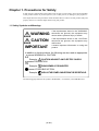
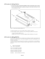
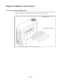
1
M306V0T-RPD-E
Emulation Pod for M16C/6V Group M306V0
User's Manual
Rev.1.00
October 16, 2003
REJ10J0380-0100Z
* IBM and PC/AT are registered trademarks of International Business Machines Corporation.
Keep safety first in your circuit designs!
• Renesas Technology Corporation and Renesas Solutions Corporation put the maximum effort into making semiconductor products better
and more reliable, but there is always the possibility that trouble may occur with them. Trouble with semiconductors may lead to personal
injury, fire or property damage. Remember to give due consideration to safety when making your circuit designs, with appropriate
measures such as (i) placement of substitutive, auxiliary circuits, (ii) use of nonflammable material or (iii) prevention against any
malfunction or mishap.
Notes regarding these materials
• These materials are intended as a reference to assist our customers in the selection of the Renesas Technology product best suited to
the customer's application; they do not convey any license under any intellectual property rights, or any other rights, belonging to Renesas
Technology Corporation, Renesas Solutions Corporation or a third party.
• Renesas Technology Corporation and Renesas Solutions Corporation assume no responsibility for any damage, or infringement of any
third-party's rights, originating in the use of any product data, diagrams, charts, programs, algorithms, or circuit application examples
contained in these materials.
• All information contained in these materials, including product data, diagrams, charts, programs and algorithms represents information
on products at the time of publication of these materials, and are subject to change by Renesas Technology Corporation and Renesas
Solutions Corporation without notice due to product improvements or other reasons. It is therefore recommended that customers contact
Renesas Technology Corporation, Renesas Solutions Corporation or an authorized Renesas Technology product distributor for the latest
product information before purchasing a product listed herein. The information described here may contain technical inaccuracies or
typographical errors. Renesas Technology Corporation and Renesas Solutions Corporation assume no responsibility for any damage,
liability, or other loss rising from these inaccuracies or errors. Please also pay attention to information published by Renesas Technology
Corporation and Renesas Solutions Corporation by various means, including the Renesas home page (http://www.renesas.com).
• When using any or all of the information contained in these materials, including product data, diagrams, charts, programs, and algorithms,
please be sure to evaluate all information as a total system before making a final decision on the applicability of the information and
products. Renesas Technology Corporation and Renesas Solutions Corporation assume no responsibility for any damage, liability or
other loss resulting from the information contained herein.
• Renesas Technology semiconductors are not designed or manufactured for use in a device or system that is used under circumstances
in which human life is potentially at stake. Please contact Renesas Technology Corporation, Renesas Solutions Corporation or an
authorized Renesas Technology product distributor when considering the use of a product contained herein for any specific purposes,
such as apparatus or systems for transportation, vehicular, medical, aerospace, nuclear, or undersea repeater use.
• The prior written approval of Renesas Technology Corporation and Renesas Solutions Corporation is necessary to reprint or reproduce
in whole or in part these materials.
• If these products or technologies are subject to the Japanese export control restrictions, they must be exported under a license from the
Japanese government and cannot be imported into a country other than the approved destination. Any diversion or reexport contrary to
the export control laws and regulations of Japan and/or the country of destination is prohibited.
• Please contact Renesas Technology Corporation or Renesas Solutions Corporation for further details on these materials or the products
contained therein.
Precautions to be taken when using this product
• This product is a development supporting unit for use in your program development and evaluation stages. In mass-producing your
program you have finished developing, be sure to make a judgment on your own risk that it can be put to practical use by performing
integration test, evaluation, or some experiment else.
• In no event shall Renesas Solutions Corporation be liable for any consequence arising from the use of this product.
• Renesas Solutions Corporation strives to renovate or provide a workaround for product malfunction at some charge or without charge.
However, this does not necessarily mean that Renesas Solutions Corporation guarantees the renovation or the provision under any
circumstances.
• This product has been developed by assuming its use for program development and evaluation in laboratories. Therefore, it does not fall
under the application of Electrical Appliance and Material Safety Law and protection against electromagnetic interference when used in
Japan.
• Do not attempt to modify this equipment. If modified, your authority to operate this equipment might be voided by FCC.
Note: This equipment has been tested and found to comply with the limits for a Class A digital device, pursuant to part 15 of the FCC Rules.
These limits are designed to provide reasonable protection against harmful interference when the equipment is operated in a commercial
environment. This equipment generates, uses, and can radiate radio frequency energy and, if not installed and used in accordance with
the user's manual, may cause harmful interference to radio communications. Operation of this equipment in a residential area is likely
to cause harmful interference in which case the user will be required to correct the interference at his own expense.
Warning: This is a Class A product. In a domestic environment this product may cause radio interference in which case the user may be
required to take adequate measures.
For inquiries about the contents of this document or product, fill in the text file the installer of the emulator debugger generates in the
following directory and email to your local distributor.
\SUPPORT\Product-name\SUPPORT.TXT
Renesas Tools Homepage http://www.renesas.com/en/tools
( 2 / 48 )
Preface
The M306V0T-RPD-E is an emulation pod for the M16C/6V group of Renesas 16-bit MCUs. The
M306V0T-RPD-E is used by being connected to the PC4701 emulator (PC4701HS, PC4701L,
PC4700H or PC4700L) and is controlled by the emulator debugger.
This manual mainly explains specifications and setting up of the M306V0T-RPD-E. For detail
information about the PC4701 emulator and the emulator debugger, refer to each user's manual.
To check the components of this product, refer to "Things to Check When Unpacking" in this manual.
If there is any question or doubt about this product, contact your local distributor.
To use the product properly
Precautions for Safety
• In both this user's manual and on the product itself, several icons are used to insure
proper handling of this product and also to prevent injuries to you or other persons,
or damage to your properties.
• The icons' graphic images and meanings are given in "Chapter 1. Precautions for
Safety". Be sure to read this chapter before using the product.
When using outside Japan
• When using in Europe, the United States, or Canada, be sure to use both the emulator
and the emulation pod which meet local standards. EMI standards are not met when
this product is used with the PC4700H or PC4700L emulator.
( 3 / 48 )
Contents
Terminology ........................................................................................................................... 6
Things to Check When Unpacking ......................................................................................... 7
Chapter 1. Precautions for Safety .......................................................................................... 8
1.1 Safety Symbols and Meanings .............................................................................. 8
1.2 Precautions for Safety ........................................................................................... 9
Warning
Warning for Installation ................................................................................... 9
Warning for Use Environment ......................................................................... 9
Caution
Cautions to Be Taken for This Product ........................................................... 9
Caution for Installation .................................................................................... 9
Important
Notes on PC4701 Emulators .......................................................................... 10
Notes on Abnormal Operation ....................................................................... 10
Notes on Target System ................................................................................. 10
Notes on Connecting Target System ............................................................. 11
Note on Reset Input from Target System ...................................................... 11
Note on HOLD Input from Target System .................................................... 11
Note on Address 0 Access ............................................................................. 11
Notes on Differences between Actual MCU and Emulator ........................... 12
Notes on MAP Settings and References ........................................................ 14
Note on Changing Data in OSD RAM Area When Program is not Executed ......... 14
Note on Reading MCU Internal Sources ....................................................... 15
Note on Stack ................................................................................................. 15
Chapter 2. Introduction ......................................................................................................... 16
Chapter 3. Specifications ...................................................................................................... 17
Chapter 4. Settings for Target Systems ................................................................................ 18
4.1 Positions of Switches .......................................................................................... 18
4.2 Settings ................................................................................................................ 19
4.3 Procedure for Setting Oscillation Frequency ...................................................... 20
4.4 Data Slicer I/O Signals and OSD Clock I/O Signal Circuits .............................. 23
4.5 Procedure for Setting Switches ........................................................................... 25
4.6 Procedure for Writing MCU File ........................................................................ 25
( 4 / 48 )
Chapter 5. Method of Connection ........................................................................................ 26
5.1 Connecting Emulator Main Unit ......................................................................... 26
5.2 Connecting Target System .................................................................................. 28
Chapter 6. Constraints .......................................................................................................... 29
Chapter 7. Operation Timing (Memory Expansion and Microprocessor Modes) ................ 30
7.1 Separate Bus (no wait) ........................................................................................ 30
7.2 Separate Bus (with wait), When Accessing to External Memory Area .............. 32
7.3 Multiplex Bus (with wait), When Accessing to External Memory Area ............ 34
7.4 Timing Requirements .......................................................................................... 37
Chapter 8. Electrical Characteristics .................................................................................... 39
Chapter 9. Maintenance and Guarantee ................................................................................ 40
9.1 Maintenance ........................................................................................................ 40
9.2 Guarantee ............................................................................................................ 40
9.3 Repair Provisions ................................................................................................ 40
9.4 How to Request for Repair .................................................................................. 41
Chapter 10. Troubleshooting ................................................................................................ 42
10.1 When M306V0T-RPD-E Does Not Work Properly ......................................... 42
Appendix A. External Dimensions ....................................................................................... 43
A.1 External Dimensions of the M306V0T-RPD-E ................................................. 43
A.2 External Dimensions of the FLX-100LCC ........................................................ 44
Appendix B. Connection Diagrams ...................................................................................... 45
( 5 / 48 )
Terminology
Some specific words used in this User's Manual are defined as follows:
PC4701
This means the generic name of the PC4701HS, PC4701L, PC4700H, and PC4700L emulators.
PC4701 system
This means an emulator system built around a PC4701 emulator. The PC4701 emulator system is
configured with the emulator main unit, an emulation pod, an emulator debugger, and a host machine.
Emulator debugger
This means a software tool to control the emulator from the host machine through an interface.
Emulator debugger: M3T-PD30 (V.3.00 Release 1 or later)
Host machine: IBM PC/AT or compatible
OS: Windows 95 or Windows NT 4.0
CPU: 486DX4-100 MHz or Pentium 75 MHz (or faster recommended)
Memory: 16 MB or more
Target MCU
This means the microcomputer you are going to debug.
Target system
This means a user's application system using the microcomputer to be debugged.
( 6 / 48 )
Things to Check When Unpacking
The M306V0T-RPD-E consists of the following parts and manuals. When unpacking, check to see
if your M306V0T-RPD-E package contains all of these items.
M306V0T-RPD-E (Emulation pod)
1
FLX120-RPD (Flexible cable for connecting PC4701 emulator)
1
Screws for connecting PC4701 emulator
2
FLX100 (Flexible cable for connecting target system, already connected)
1
FLX-100LCC (Converter board for 100LCC package)
1
OSC-2 (Oscillator board)
1
M306V0T-RPD-E English user's manual (this manual)
1
M306V0T-RPD-E Japanese user's manual
1
If any of these items are missing or found faulty, please contact your local distributor. Also, if there
is any question or doubt about the packaged products, contact your local distributor.
CAUTION
Please keep the M306V0T-RPD-E’s packing box and cushion material in your place for reuse at a
later time when sending your product for repair or other purposes. Always use these packing box and
cushion material when transporting the M306V0T-RPD-E.
( 7 / 48 )
Chapter 1. Precautions for Safety
In both the user's manual and on the product itself, several icons are used to insure proper handling
of this product and also to prevent injuries to you or other persons, or damage to your properties.
This chapter describes the precautions which should be taken in order to use this product safely and
properly. Be sure to read this chapter before using this product.
1.1 Safety Symbols and Meanings
WARNING
If the requirements shown in the "WARNING"
sentences are ignored, the equipment may
cause serious personal injury or death.
CAUTION
If the requirements shown in the "CAUTION"
sentences are ignored, the equipment may
malfunction.
IMPORTANT
It means important information on using this
product.
In addition to the three above, the following are also used as appropriate.
means WARNING or CAUTION.
Example:
CAUTION AGAINST AN ELECTRIC SHOCK
means PROHIBITION.
Example:
DISASSEMBLY PROHIBITED
means A FORCIBLE ACTION.
Example:
UNPLUG THE POWER CABLE FROM THE RECEPTACLE.
The following pages describe the symbols "WARNING", "CAUTION", and "IMPORTANT".
( 8 / 48 )
1.2 Precautions for Safety
WARNING
Warning for Installation:
• Do not set this product in water or areas of high humidity. Spilling water or some other liquid into
the main unit can cause an unrepairable damage.
Warning for Use Environment:
• This equipment is to be used in an environment with a maximum ambient temperature of 35°C. Care
should be taken that this temperature is not exceeded.
CAUTION
Cautions to Be Taken for This Product:
• Do not disassemble or modify this product as personal. Disassembling or modifying this product
can cause damage.
• Use caution when handling the main unit. Be careful not to apply a mechanical shock.
• Do not touch directly the connector pins of the emulator main unit or the target MCU connector pins
with your hand.
• Do not pull the emulation pod main unit by the FLX120-RPD flexible cable or the FLX100 flexible
cable for connecting the target system.
• The flexible cables FLX120-RPD and FLX100 are different from earlier models. The slits make
them more flexible. However, excessive flexing or force may break conductors.
• Do not use inch-size screws for this equipment. The screws used in this equipment are all ISO
(meter-size) type screws. When replacing screws, use same type screws as used on the equipment.
Cautions for Installation:
• Do not place the main unit on its side when in use.
( 9 / 48 )
IMPORTANT
Notes on PC4701 Emulators:
• The PC4700H emulators whose serial number ends with a number cannot be used with M306V0TRPD-E. Use only products whose serial number ends with a letter of the alphabet. The serial number
is on the bottom of the PC4700H.
Example: 5KE100 ........ Can NOT be used with M306V0T-RPD-E.
Requires an upgrade.
Example: 5LE123B ...... Can be used with M306V0T-RPD-E.
• Do not turn off the power when downloading firmware. If the emulator is powered off in the middle
of the process, it will become unable to start up normally. In cases when the power is inadvertently
shut off, re-execute downloading.
Notes on Abnormal Operation:
• If the PC4701 system does not pass all self-checks (excluding when an target system error occurs),
there is the possibility of trouble in the system. In such case, contact the place of purchase.
Please take note that self-check should be executed under the following conditions.
(1) The target system is not connected.
(2) The Switch SW6 is set to 'L' position, SW7 to '16' (see Chapter 4).
• If the emulator malfunctions due to external interference or some other causes, follow the steps
given below.
(1) Press the system reset switch located on the front panel of the emulator.
(2) If the emulator does not return to the normal operation despite the step (1) above, turn off the
power source of the emulator, turn it on again.
Notes on Target System:
• Because the emulation pod does not have the capacity to supply power to other devices, design your
system so that the emulator MCU is powered by the target system.
• Make sure that the target's supply voltage is within the MCU specification and in the range of +4.5
to 5.5 V.
• Do not change power supply voltage of the target system after activating the power.
• Before turning on power to anything, check the host machine, emulator main unit, emulation pod,
conversion board and user's target system are properly connected. Activate power to units as
explained here following.
(1) Turn on and off power to the target system, and then the PC4701 continuously.
(2) After turning on power to the PC4701, check the Target Status LEDs on the emulator' front
panel to see if the M306V0T-RPD-E is ready to operate.
• Is the power supplied? Check that Target Status LED (POWER) is on.
• Is the reset released? Check that Target Status LED (RESET) is off.
( 10 / 48 )
IMPORTANT
Notes on Connecting Target System:
• When connecting the FLX100 flexible cable and the converter board, be careful not to forcibly
press the connector top of the converter board. (The flexible cable and the converter board are
guaranteed for only 20 insertion/removal iterations.)
• Especially be careful not to insert the converter board in the wrong direction.
Note on Reset Input from Target System:
• The reset input from the target system is accepted only during program execution (while the RUN
signal lamp on the PC4701 is lit).
Note on HOLD Input from Target System:
• Input an 'L' level signal into the HOLD pin only during program execution. Doing so while the
program is stopped or during run time debugging may cause the emulator to malfunction.
Note on Address 0 Access:
• With M16C/6V group MCUs, when a maskable interrupt is generated, the interrupt data (interrupt
number and interrupt request level) stored in address 0 is read out.
Also, the interrupt request bit is cleared when address 0 is read out. Consequently, when the address
0 readout instruction is executed or when address 0 is read out in the cause of a program runaway,
a malfunction occurs in that the interrupt is not executed despite the interrupt request, because the
request bit of the highest priority interrupt factor enabled is cleared.
Therefore, with M306V0T-RPD-E, if address 0 is read out for anything other than interrupt
processing, the yellow LED lights up as a warning. When this LED lights up, there is the possibility
of illegal access to address 0, therefore check the program. This LED is extinguished from the
emulator reset switch.
( 11 / 48 )
IMPORTANT
Notes on Differences between Actual MCU and Emulator:
• Emulator operation differs from mask MCU operation, as listed below:
(1) Reset condition
(2) Initial values of internal resource data at power-on
(3) Internal RAM and ROM capacities, etc.
(4) Ports P00 to P57
Of the M306V0T-RPD-E's I/O ports, ports P00 - P57 are connected to the user's target system
through the port emulation circuit inside M306V0T-RPD-E.
Table 1.1 gives the device which uses these ports.
Table 1.1 I/O device used by each of the ports
Port
I/O device
P00-P57
M60074-0111FP
(5) Writing into pullup control registers 0 and 1 (addresses 03FC16 and 03FD16 respectively)
To write into pullup control registers 0 and 1 (addresses 03FC16 and 03FD16 respectively), it
is necessary to write the word data from address 03FC16. This is an M306V0T-RPD-E
restriction.
(6) Ports P50 - P53
To enable pullup when setting bit 2 (PUR12) of the pullup register 1 to '1' in single chip mode,
be sure to set the bit 2 (PM02) and bit 7 (PM07) of the processor mode register 0 to '0'. This
is an M306V0T-RPD-E restriction.
(7) BCLK output disable
To disable the BCLK output, it is necessary to set the BCLK output disable bit (PM07) of
processor mode register 0 (address 000416) to '1' and to set bit 3 of the port P5 direction register
(address 03EB16) to '0'. This is an M306V0T-RPD-E restriction.
(8) Hold control
When an 'L' level signal is input to the terminal HOLD and the terminal enters the hold state,
in actuality, ports P00 to P52 enter the hold state one half cycle later than the MCU (see Chapter
7, Operation Timing).
(9) A/D converter
A/D converter characteristics differ from actual MCU characteristics because the flexible
cable and other elements are used between the emulation MCU and user’s target.
(10) Status while the program is stopped
In a system using the PC4701, the loop iteration at the address F800016 establishes and
maintains the status during program stop. Also, when debug commands are issued to check
or edit memory data, addresses F800016 to F83FF16 and addresses F600016 to F63FF16 are used
as work area. For this reason, when the CS0 output is enabled in the microprocessor mode,
the CS0 signal is output.
( 12 / 48 )
IMPORTANT
(11) Actual MCU output and emulator output
Table 1.2 Actual MCU and emulator outputs
Access area
SFR area
Signal
Actual MCU
M306V0T-RPD-E
Address
Output
Output
Data
Output (Floating during
Floating
read operations)
RD/WR
CS
ALE
RD=Low at read cycle)
(High output fixed)
No output
No output
(High output fixed)
(High output fixed)
No output
Output
Output
Output
Internal RAM area
Address
Previous status maintained
Output
Internal ROM area
Data
Floating
Floating
RD/WR
No output
No output
(High output fixed)
(High output fixed)
No output
No output
(High output fixed)
(High output fixed)
No output
Output
No output (Previous
Output
*
status maintained)
External area
Address
Output
Output
Data
Output (Inputs external
Output (Inputs external
data when reading)
data when reading)
RD/WR
In STOP state
Output (WR=Low at write cycle, Output (WR=Low at write cycle,
RD=Low at read cycle)
RD=Low at read cycle)
CS
Output
Output
ALE
Output
Output
BHE
Output
Output
Address
Output
Data
Floating
RD/WR
Output only for Read operations
(WR = High output fixed)
CS
Output
ALE
Output
BHE
Output
( 13 / 48 )
*
*
(Low output fixed)
BHE
*
*
BHE
ALE
*
Output (WR=Low at write cycle, No output
(Low output fixed)
CS
Item with
different
outputs
IMPORTANT
Notes on MAP Settings and References:
• For details on MAP settings and references, refer to the M3T-PD30 emulator debugger user's
manual.
• Always set the SFR area to EXTERNAL.
• Set the OSD RAM area to INTERNAL.
• This pod uses the 4 bytes from 0FFFC16 to 0FFFF16 as a stack area for a RESET command. The
RESET command cannot be correctly executed when these 4 bytes cannot be read or written to.
You must therefore take care using the MAP resetting procedure when the following condition (1)
or condition (2) are true.
(1) When the 4 bytes from 0FFFC16 to 0FFFF16 are set to EXTERNAL in a system shifting from
single chip mode to memory expansion mode or microprocessor mode
(2) When the 4 bytes from 0FFFC16 to 0FFFF16 are set to EXTERNAL in a system started in
microprocessor mode and there is no read/write-enabled memory in the external area.
Use the following MAP setting procedure when either of the above conditions (1) or (2) are true.
(1) Set the 4 bytes from bytes from 0FFFC16 to 0FFFF16 to INTERNAL.
(2) Execute the M3T-PD30 emulator debugger RESET command.
(3) Set the stack pointer.
(Example)
RESET:
FCLR I
LDC #480H, SP <- stack pointer setting
:
(STOP the program after executing this command.)
(4) Set the 4 bytes from 0FFFC16 to 0FFFF16 to EXTERNAL.
Note on Changing Data in OSD RAM Area When Program is not Executed:
• To change data when a program is not executed, write data when the map setting is in both
'INTERNAL' and 'EXTERNAL'.
Procedure
(1) With 'INTERNAL' specified, change data in the OSD RAM area.
Change data in the MEMORY WINDOW, Script Window, etc.
(2) From the script window, change the map setting of the OSD RAM area to 'EXTERNAL' .
MAP 400,FFF,EXT
(3) With 'EXTERNAL' specified, change data in the OSD RAM area.
Change data in the MEMORY WINDOW, Script Window, etc.
(4) Change the map setting of the OSD RAM area to 'INTERNAL' again.
MAP 400,FFF,INT
(Example) When changing the data in the OSD RAM area (Address: 410h) to '55h'.
set MemoryByte( MB ) 410,55
MAP 400,FFF,EXT
set MemoryByte( MB ) 410,55
MAP 400,FFF,INT
( 14 / 48 )
IMPORTANT
Note on Reading MCU Internal Sources:
• When this product is configured with the emulator debugger, the following results occur when
reading the registers listed in Table 1.3. Data is not displayed correctly, but internal data is not
affected at all.
(1) Real-time tracing
Data values in the MCU internal source read cycle are not displayed correctly.
(2) Real-time RAM monitoring
Data is not displayed correctly.
This happens because data read from the MCU internal source is not output to an external
point. When data is written into an MCU internal source, the data input from the external point
is displayed correctly.
Table 1.3 Registers and signals
Register
Signal
Processor mode registers 0, 1
PM0, PM1
System clock control registers 0, 1
CM0, CM1
Chip select control register
CSR
Address identity interrupt enable register
AIER
Protect register
PRCR
Supervisor timer start register
WDTS
Supervisor timer control register
WDC
Address identity interrupt registers 0, 1
RMAD0, RMAD1
DMA source pointers 0, 1
SAR0, SAR1
DMA destination pointers 0, 1
DAR0, DAR1
DMA transfer counters 0, 1
TCR0, TCR1
DMA control registers 0, 1
DM0CON, DM1CON
Note on Stack:
• This product uses up to 8 bytes for stack.
( 15 / 48 )
Chapter 2. Introduction
M306V0T-RPD-E is used by being connected to the PC4701 emulator main unit. Figure 2.1 shows
the system configuration.
Figure 2.1 System configuration
Following products (1) to (4) are attached to M306V0T-RPD-E.
(1) Emulation pod (M306V0T-RPD-E)
This emulation pod contains emulation memory and debug functions.
(2) Flexible cable (FLX120-RPD)
This 120-pin flexible cable connects the PC4701 and the emulation pod.
(3) Flexible cable (FLX100)
This 100-pin flexible cable connects the emulation pod and the target system.
(4) Converter board (FLX-100LCC)
This board is connected to a socket for 100LCC on the target system.
( 16 / 48 )
Chapter 3. Specifications
Table 3.1 lists the specifications of the M306V0T-RPD-E.
Table 3.1 Specifications of the M306V0T-RPD-E
Description
Item
Usable emulator
PC4701HS, PC4701L
Usable MCU
M16C/6V Group MCUs
Usable MCU modes
(1) Single-chip mode
(2) Memory expansion mode
(3) Microprocessor mode
Evaluation MCU type
M306V0EEFP
Emulation pod clock
Main clock (Xin): 10.000 MHz
Sub-clock (Xcin): 32.768 kHz
Max. operating frequency of emulation pod
10 MHz, 0-wait (Vcc = 5.0 V)
Power supply range
4.5 to 5.5 V
Emulation memory
1 MB
Stack capacity used for emulator
Up to 8 bytes
Suspended cycles in run-time debug
16-byte dump: About 312 BCLK cycle
16-byte fill: About 283 BCLK cycle
Power supply to pod
1. Supplied from an emulator
2. The operating voltage of the emulation pod is
determined by detecting the supply voltage of the
target system. When no target system is connected,
or when the supply voltage of the target system is
more than 5.0 V, the operating voltage is 5.0 V.
Connection with target system
100-pin LCC package: via FLX-100LCC
Operating temperature range
5 to 35°C (no dew)
Storage temperature range
-10 to 60°C
Overseas standards
• EMI standards (FCC part15 Class A)
• CE marking (EN55022, EN50082-1)
( 17 / 48 )
Chapter 4. Settings for Target Systems
4.1 Positions of Switches
Figure 4.1 shows positions of switches on the M306V0T-RPD-E.
Figure 4.1 Positions of switches
( 18 / 48 )
4.2 Settings
Table 4.1 gives a list of switch settings.
Table 4.1 Switch (SW) settings
Signal
SW No.
Setting
To use port P57
PORT/OSD
(P57)
PORT
(P57)
SW1
To use OSD function
OSD
PORT
(P57)
PORT
(Factory-setting)
P87
SW2
P87
XCIN
XCIN
P87
(Factory-setting)
P86/XCOUT
SW3
P86
XCIN
To use XCOUT terminal
To leave unconnected
To use port P86
P86
XCOUT
OSD
To use XCIN terminal
To use port P87
P87/XCIN
OSD
XCOUT
P86
P86
(Factory-setting)
XCOUT
To connect XOUT terminal
To open
XOUT
P55/HOLD
P57/RDY
OPEN
SW4
XOUT
OPEN
XOUT
With pullup resistor (HOLD/RDY)
Without pullup resistor
H
SW5
OPEN
H
H
(Factory-setting)
SW6
XOUT
OPEN
(Factory-setting)
L
L
H
XOUT
OPEN
To pull up 33 kΩ
To leave unconnected
To pull down 33 kΩ
CNVss
H
L
L
(Factory-setting)
SW7
16
To pull up 33 kΩ
To leave unconnected
16
8
8
16
16
(Factory-setting)
SW8
H
8
8
With pullup resistor
P70/71
H
H
To pull down 33 kΩ
BYTE
XCOUT
OPEN
H
Without pullup resistor
H
OPEN
OPEN
(Factory-setting)
* Leave the SW1 in the PORT position.
IMPORTANT
Note on Switch Settings:
• Be sure to turn off the power before setting the switches. Otherwise, the internal
circuits may be damaged.
( 19 / 48 )
4.3 Procedure for Setting Oscillation Frequency
If you are using the emulation pod's internal oscillator, see (1) below. If you are using the target
system's oscillator, see (2) on page 22.
(1) Using emulation pod's oscillator
M306V0T-RPD-E is available with two types of internal oscillator circuits:
• OSC-3 oscillator board (preinstalled in M306V0T-RPD-E): 10 MHz
• OSC-2 oscillator board (bare board)
(a) OSC-3 oscillator board
M306V0T-RPD-E is equipped with a 10MHz internal oscillator board. If you are running
M306V0T-RPD-E at 10 MHz, you can use the OSC-3 oscillator board shipped with.
(b) OSC-2 oscillator board
M306V0T-RPD-E is supplied with an oscillator circuit bare board (connector pin mounting).
If you are using M306V0T-RPD-E with internal oscillation frequencies other than those
permitted by the standard OSC-3 oscillator board, create the desired oscillator circuit on the OSC2 bare board and replace the OSC-3 board with the OSC-2 board.
Figure 4.2 shows the external dimensions and connector pin layout of the OSC-2 oscillator board.
Figure 4.3 shows the OSC-2 circuit. Use the circuit constants recommended by the maker of the
oscillator circuit.
J1-4: GND
J1-3: Oscillator output
J1-2: GND
J1-1: VCC
Figure 4.2 External view of oscillator bare board OSC-2 and connector pin assignments
( 20 / 48 )
IC1
IC1
11
10
CLK
8
9
J1-3
R1
*
*
X1 ,X 2
C2
*
Vcc
1
2
3
4
5
6
7
13
12
GND
R2
C1
X3
C3
14
IC1
J1-2
J1-4
IC1
* X1: 5.08-mm-pitch 2-pin oscillator
* X2: 2.54-mm-pitch 2-pin oscillator
* X3: 2.54-mm-pitch 3-pin oscillator
J1-1
GND
IC1: Inverter (Unbuffer)
Figure 4.3 Circuit of oscillator board OSC-2
Figure 4.4 shows how to replace the oscillator board.
(a) Remove the screw locking the oscillator board in place.
(b) Lift the board directly up and out of the product.
(c) Plug the J1 connector of the new oscillator board into the J7 connector on the M306V0T-RPDE board.
(d) Lock the board to the M306V0T-RPD-E board with the screw.
Figure 4.4 Replacing oscillator board
( 21 / 48 )
(2) Using target system's oscillator
a. To operate the emulator with an external clock, construct the oscillation circuit shown in
Figure 4.5 in the target system and input the oscillation output at 40-60% duty (within the
operating range of the emulator's MCU) into the Xin (Xcin) pin.
b. Make note of the fact that in the oscillation circuit shown in Figure 4.6 where a resonator
is connected between the Xin (Xcin) and Xout (Xcout) pins, oscillation does not occur
because a flexible cable, buffer IC and other devices are used between the evaluation MCU
and the target system.
c. Use the M3T-PD30 emulator debugger to set CLK to EXT. For details, see the M3T-PD30
emulator debugger user's manual.
Figure 4.5 External oscillator circuit
Figure 4.6 Circuit for no oscillation in this pod
( 22 / 48 )
4.4 Data Slicer I/O Signals and OSD Clock I/O Signal Circuits
Figure 4.7 shows the layout of the parts on the board and the circuit diagrams used for data slicing
and the OSD clock circuits.
Figure 4.7 Layout of parts
(1) Figure 4.8 shows the part numbers and the constants of the parts of the signal CVIN.
Figure 4.8 CVIN signal circuit
(2) Figure 4.9 shows the part numbers and the constants of the parts of the signal HLF.
Figure 4.9 HLF signal circuit
( 23 / 48 )
(3) Figure 4.10 shows the part numbers and the constants of the parts of the signal VHOLD.
Figure 4.10 VHOLD signal circuit
(4) Figure 4.11 shows the part numbers and the constants of the parts of the signal OSC1, OSC2.
Figure 4.11 OSC1, OSC2 signal circuit
( 24 / 48 )
4.5 Procedure for Setting Switches
(1) You must remove the cover of the M306V0T-RPD-E in order to set the switches. To do so, remove
the four screws holding the top cover. There are two screws on each side (see Figure 4.12). Be
sure to turn OFF the power before attempting to change the switch settings. If the power is ON,
you may damage the circuits.
Figure 4.12 Removing M306V0T-RPD-E cover
(2) After removing the cover, set the switches referring to Table 4.1 (page 19).
(3) After setting the switches, replace the cover by reversing the procedure for its removal.
1. Replace the M306V0T-RPD-E cover.
2. Replace the screws (two on each side) holding the M306V0T-RPD-E cover in place.
4.6 Procedure for Writing MCU File
You may need to change the contents of the MCU file, depending on the MCU being developed. The
MCU file is in the same directory as the emulator debugger. The file name is M30620.MCU for the
M16C/6V group MCUs.
The MCU file contains the following information: SFR area, internal RAM area, internal ROM area,
and firmware filename. Set these according to the MCU being developed. Use your editor to edit the
MCU file.
0
SFR area starting address
3FF
SFR area ending address
2C00 Internal RAM starting address
3FFF Internal RAM ending address
F0000 Internal ROM starting address
FFFFFInternal ROM ending address
M30620B
Firmware filename (Do not edit.)
( 25 / 48 )
Chapter 5. Method of Connection
5.1 Connecting Emulator Main Unit
Use the FLX120-RPD 120-pin flexible cable to connect the emulator main unit and M306V0T-RPDE. Figure 5.1 shows how to connect the emulator main unit and FLX120-RPD.
Figure 5.1 Connecting emulator main unit and FLX120-RPD
( 26 / 48 )
Connect FLX120-RPD with M306V0T-RPD-E. Figure 5.2 shows how to connect M306V0T-RPDE and FLX120-RPD.
Figure 5.2 Connecting M306V0T-RPD-E and FLX120-RPD
CAUTION
Note on Connecting the Cable:
• Always shut OFF power before connecting the cable. The power ON state could
destroy internal circuits.
( 27 / 48 )
5.2 Connecting Target System
Figure 5.3 shows connections between emulator probes and target systems. For more details, refer
to "Renesas Tools - Accessory Guide".
Figure 5.3 Connection to target systems
CAUTION
Notes on Connecting the Target Systems:
• Be sure to turn off the power before making connections. Otherwise, the internal
circuits may be damaged.
• The small connectors of the FLX100 and FLX-100LCC are guaranteed for only 20
insertion/removal iterations.
( 28 / 48 )
Chapter 6. Constraints
(1) BRK instruction
The BRK instruction cannot be used.
(2) Software and hardware breaks
a. Do not set simultaneous software and hardware breaks.
b. Do not use software breaks for areas for which the MAP setting is EXTERNAL.
(3) Using multiplex bus with the PC4701L emulator
You can only use Fetch as a hardware break condition for the multiplex bus area.
(4) Using address match interrupts
a. Do not set a software break at the same address as you have set an address match interrupt.
b. Do not set a hardware break within the 4 bytes leading up to the address at which an address
match interrupt is invoked.
c. When the address at which an address match interrupt occurs is achieved by one-step
execution, the address match interrupt processing and the first command on return from
the interrupt are executed simultaneously.
(5) Software resets
Do not use software resets.
(6) Watchdog function
If using the watchdog function, you can only use program execution. If you want to use debugger
functions other than program execution, disable the watchdog function.
( 29 / 48 )
Chapter 7. Operation Timing (Memory Expansion and Microprocessor Modes)
7.1 Separate Bus (no wait)
Table 7.1 and Figure 7.1 show bus timing when using the memory expansion mode and microprocessor mode (separate bus, no wait).
Table 7.1 Memory expansion mode and microprocessor mode (separate bus, no wait)
Parameter
Symbol
M306V0EEFP
[ns]
M306V0T-RPD-E
[ns]
Min.
Max.
Min.
Max.
td(BCLK-AD)
Address output delay time
-
25
-
47
th(BCLK-AD)
Address output hold time (BCLK)
4
-
4
-
th(RD-AD)
Address output hold time (RD)
0
-
-5
-
th(WR-AD)
Address output hold time (WR)
0
-
-3
-
td(BCLK-CS)
Chip-select output delay time
-
25
-
36
th(BCLK-CS)
Chip-select output hold time (BCLK)
4
-
4
-
td(BCLK-ALE)
ALE signal output delay time
-
25
-
14
th(BCLK-ALE)
ALE signal output hold time
-4
-
-4
-
td(BCLK-RD)
RD signal output delay time
-
25
-
40
th(BCLK-RD)
RD signal output hold time
0
-
0
-
td(BCLK-WR)
WR signal output delay time
-
25
-
40
th(BCLK-WR)
WR signal output hold time
0
-
0
-
td(BCLK-DB)
Data output delay time (BCLK)
-
40
-
70
th(BCLK-DB)
Data output hold time (BCLK)
4
-
2
-
td(DB-WR)
Data output delay time (WR)
(Note 1)
-
(Note 2)
-
th(WR-DB)
Data output hold time (WR)
0
-
0
-
Note 1. Compute bus timing according to BCLK frequency. Use the below formula.
td(DB-WR) =
109
- 40 [ns]
f(BCLK)x2
Note 2. Compute bus timing according to BCLK frequency. Use the below formula.
td(DB-WR) =
- 55 [ns]
109
f(BCLK)x2
( 30 / 48 )
Vcc = 5 V
Memory expansion mode or microprocessor mode (no wait)
Read timing
Write timing
Measurement Condition
• VCC = 5 V
• Input timing voltage: VIL = 0.8 V, VIH = 2.5 V
• Output timing voltage: VOL = 0.8 V, VOH = 2.0 V
Figure 7.1 Memory expansion mode and microprocessor mode (separate bus, no wait)
( 31 / 48 )
7.2 Separate Bus (with wait), When Accessing to External Memory Area
Table 7.2 and Figure 7.2 show bus timing when using the memory expansion mode and microprocessor mode (with wait, when accessing to the external memory area).
Table 7.2 Memory expansion mode and microprocessor mode (separate bus, with wait)
Parameter
Symbol
M306V0EEFP
[ns]
M306V0T-RPD-E
[ns]
Min.
Max.
Min.
Max.
td(BCLK-AD)
Address output delay time
-
25
-
47
th(BCLK-AD)
Address output hold time (BCLK)
4
-
4
-
th(RD-AD)
Address output hold time (RD)
0
-
-5
-
th(WR-AD)
Address output hold time (WR)
0
-
-3
-
td(BCLK-CS)
Chip-select output delay time
-
25
-
36
th(BCLK-CS)
Chip-select output hold time (BCLK)
4
-
4
-
td(BCLK-ALE)
ALE signal output delay time
-
25
-
14
th(BCLK-ALE)
ALE signal output hold time
-4
-
-4
-
td(BCLK-RD)
RD signal output delay time
-
25
-
40
th(BCLK-RD)
RD signal output hold time
0
-
0
-
td(BCLK-WR)
WR signal output delay time
-
25
-
40
th(BCLK-WR)
WR signal output hold time
0
-
0
-
td(BCLK-DB)
Data output delay time (BCLK)
-
40
-
70
th(BCLK-DB)
Data output hold time (BCLK)
4
-
2
-
td(DB-WR)
Data output delay time (WR)
(Note 1)
-
(Note 2)
-
th(WR-DB)
Data output hold time (WR)
0
-
0
-
Note 1. Compute bus timing according to BCLK frequency. Use the below formula.
td(DB-WR) =
109
- 40 [ns]
f(BCLK)x2
Note 2. Compute bus timing according to BCLK frequency. Use the below formula.
td(DB-WR) =
109
- 55 [ns]
f(BCLK)x2
( 32 / 48 )
Vcc = 5 V
Memory expansion mode or microprocessor mode
(with wait, when accessing to the external memory area)
Read timing
Write timing
Measurement Condition
• VCC = 5 V
• Input timing voltage: VIL = 0.8 V, VIH= 2.5 V
• Output timing voltage: VOL = 0.8 V, VOH = 2.0 V
Figure 7.2 Memory expansion mode and microprocessor mode (separate bus, with wait)
( 33 / 48 )
7.3 Multiplex Bus (with wait), When Accessing to External Memory Area
Table 7.3 and Figure 7.3 show bus timing when using the memory expansion mode and microprocessor mode (with wait, when accessing to the external memory area).
Table 7.3 Memory expansion mode and microprocessor mode (multiplex bus, with wait)
Symbol
Parameter
M306V0EEFP
[ns]
M306V0T-RPD-E
[ns]
Min.
Max.
Min.
Max.
td(BCLK-AD)
Address output delay time
-
25
-
47
th(BCLK-AD)
Address output hold time (BCLK)
4
-
4
-
th(RD-AD)
Address output hold time (RD)
(Note 1)
-
(Note 2)
-
th(WR-AD)
Address output hold time (WR)
(Note 1)
-
(Note 2)
-
td(BCLK-CS)
Chip-select output delay time
-
25
-
36
th(BCLK-CS)
Chip-select output hold time (BCLK)
4
-
4
-
th(RD-CS)
Chip-select output hold time (RD)
(Note 1)
-
(Note 2)
-
th(WR-CS)
Chip-select output hold time (WR)
(Note 1)
-
(Note 2)
-
td(BCLK-RD)
RD signal output delay time
-
25
-
38
th(BCLK-RD)
RD signal output hold time
0
-
0
-
td(BCLK-WR)
WR signal output delay time
-
25
-
40
th(BCLK-WR)
WR signal output hold time
0
-
0
-
td(BCLK-DB)
Data output delay time (BCLK)
-
40
-
40
th(BCLK-DB)
Data output hold time (BCLK)
4
-
4
-
td(DB-WR)
Data output delay time (WR)
(Note 1)
-
(Note 2)
-
th(WR-DB)
Data output hold time (WR)
(Note 1)
-
(Note 2)
-
td(BCLK-ALE)
ALE signal output delay time (BCLK)
-
25
-
14
th(BCLK-ALE)
ALE signal output hold time (BCLK)
-4
-
-4
-
td(AD-ALE)
ALE signal output delay time (ADDRESS) (Note 1)
-
(Note 2)
-
th(ALE-AD)
ALE signal output hold time (ADDRESS)
50
-
50
-
td(AD-RD)
ALE signal output hold time (ADDRESS)
0
-
0
-
td(AD-WR)
ALE signal output hold time (ADDRESS)
0
-
0
-
tdz(RD-AD)
ALE signal output hold time (ADDRESS)
-
8
-
13
( 34 / 48 )
Note 1. Compute bus timing according to BCLK frequency. Use the below formula.
th(RD-AD) =
109
f(BCLK)x2
[ns]
td(DB-WR) =
109x3
- 40 [ns]
f(BCLK)x2
th(RW-AD) =
109
f(BCLK)x2
[ns]
th(WR-DB) =
109
f(BCLK)x2
th(RD-CS) =
109
f(BCLK)x2
[ns]
td(DB-WR) =
109
- 25 [ns]
f(BCLK)x2
th(WR-CS) =
109
f(BCLK)x2
[ns]
[ns]
Note 2. Compute bus timing according to BCLK frequency. Use the below formula.
th(RD-AD) =
109
- 10 [ns]
f(BCLK)x2
td(DB-WR) =
109x3
- 24 [ns]
f(BCLK)x2
th(RW-AD) =
109
- 10 [ns]
f(BCLK)x2
th(WR-DB) =
109
- 35 [ns]
f(BCLK)x2
th(RD-CS) =
109
- 12 [ns]
f(BCLK)x2
td(DB-WR) =
109
- 35 [ns]
f(BCLK)x2
th(WR-CS) =
109
- 12 [ns]
f(BCLK)x2
( 35 / 48 )
Vcc = 5 V
Memory expansion mode or microprocessor mode
(with wait, when accessing to the external memory area)
Read timing
Write timing
Measurement Condition
• VCC = 5 V
• Input timing voltage: VIL = 0.8 V, VIH = 2.5 V
• Output timing voltage: VOL = 0.8 V, VOH = 2.0 V
Figure 7.3 Memory expansion mode and microprocessor mode (multiplex bus, with wait)
( 36 / 48 )
7.4 Timing Requirements
Table 7.4 and Figure 7.4 show timing requirements when using the memory expansion mode and
microprocessor mode.
Table 7.4 Timing requirements (Vcc = 5 V)
Symbol
Parameter
M306V0EEFP
[ns]
M306V0T-RPD-E
[ns]
Min.
Max.
Min.
Max.
Data input setup time
40
-
80
-
tsu(RDY-BCLK) RDY input setup time
30
-
50
-
tsu(HOLD-BCLK) HOLD input setup time
40
-
(Note 1)
-
tsu(DB-RD)
th(RD-DB)
Data input hold time
0
-
0
-
th(BCLK-RDY)
RDY input hold time
0
-
0
-
th(BCLK-HOLD) HOLD input hold time
0
-
0
-
th(BCLK-HLDA) HLDA output delay time
-
40
-
40
Note 1. tsu(HOLD-BCLK) =
109x3
+ 20
f(BCLK)x2
( 37 / 48 )
Memory expansion mode or microprocessor mode
Vcc = 5 V
Note 1. P00 to P52 will be high-impedance status regardless of the input level of BYTE pin and ports P40 to P43
function selection bit (PM06) of the processor mode register 0.
Note 2. This product will be high-impedance delaying by 0.5 cycles than an actual MCU.
Measurement Condition
• VCC = 5 V
• Input timing voltage: VIL = 1.0 V, VIH = 4.0 V
• Output timing voltage: VOL = 2.5 V, VOH = 2.5 V
Figure 7.4 Timing requirements (Vcc = 5 V)
( 38 / 48 )
Chapter 8. Electrical Characteristics
Tables 8.1 and 8.2 show IC electrical characteristics of user's interface.
Table 8.1 Electrical characteristics of 74HC4066FS (P00 - P52)
Standard value
Symbol
Unit
Parameter
Vcc
Min.
Typ.
Max.
VIHC
'H' level control input voltage
2.0
4.5
1.5
3.15
-
-
V
VILC
'L' level control input voltage
2.0
4.5
-
-
0.5
1.35
V
RON
On resistance
2.0
4.5
-
2000
100
200
Ω
On resistance difference between
arbitrary 2 switches in a package
2.0
4.5
-
50
3
-
Ω
Switch input/output off leakage current
6.0
-
-
±
µA
RON
IOFF
Table 8.2 Electrical characteristics of M60074-0111FP (P53 - P57, 5 V)
Standard value
Symbol
Parameter
Unit
Min.
Typ.
Max.
VTVT+
VTH
Input voltage
1.25
2.3
0.3
-
2.3
3.7
1.2
V
VOH
'H' level output voltage
4.95
-
-
V
VOL
'L' level output voltage
-
-
0.05
V
IOH
'H' level output current
-
-
-8
mA
IOL
'L' level output current
8
-
-
mA
IIH
'H' level input current
-1
-
+1
µA
IIL
'L' level input current
-1
-
+1
µA
IOZH
Off state 'H' level output current
-1
-
+1
µA
IOZL
Off state 'L' level output current
-1
-
+1
µA
CIO
Input/output terminal capacity
-
7
15
pF
( 39 / 48 )
Chapter 9. Maintenance and Guarantee
9.1 Maintenance
If dust or dirt collects on any equipment of your emulation system, wipe it off with a dry soft cloth.
Do not use thinner or other solvents because these chemicals can cause the equipment's surface
coating to separate.
9.2 Guarantee
If your product becomes faulty within one year after its purchase while being used under good
conditions by observing "Precautions for Safety" described in Chapter 1 of this user's manual, we will
repair or replace your faulty product free of charge. Note, however, that if your product's fault is raised
by any one of the following causes, we will repair it or replace it with new one with extra-charge:
• Misuse, abuse, or use under extraordinary conditions
• Unauthorized repair, remodeling, maintenance, and so on
• Inadequate user's system or misuse of it
• Fires, earthquakes, and other unexpected disasters
In the above cases, contact your local distributor. If your product is being leased, consult the leasing
company or the owner.
9.3 Repair Provisions
(1) Repair with extra-charge
The products elapsed more than one year after purchase can be repaired with extra-charge.
(2) Replacement with extra-charge
If your product's fault falls in any of the following categories, the fault will be corrected by
replacing the entire product instead of repair, or you will be advised to purchase new one,
depending on the severity of the fault.
• Faulty or broken mechanical portions
• Flaw, separation, or rust in coated or plated portions
• Flaw or cracks in plastic portions
• Faults or breakage caused by improper use or unauthorized repair or modification
• Heavily damaged electric circuits due to overvoltage, overcurrent or shorting of power supply
• Cracks in the printed circuit board or burnt-down patterns
• Wide range of faults that makes replacement less expensive than repair
• Unlocatable or unidentified faults
(3) Expiration of the repair period
When a period of one year elapses after the model was dropped from production, repairing
products of the model may become impossible.
(4) Transportation fees at sending your product for repair
Please send your product to us for repair at your expense.
( 40 / 48 )
9.4 How to Request for Repair
If your product is found faulty, follow the procedure below to send your product for repair.
Customer
Fill in the Repair Request Sheet included with this product, then send it
along with this product for repair to your local distributor. Make sure
that information in the Repair Request Sheet is written in as much detail
as possible to facilitate repair.
Distributor
After checking the contents of fault, the distributor should please send
the faulty product along with the Repair Request Sheet to Renesas
Solutions Corp.
Renesas Solutions
When the faulty product is repaired, it will be returned to the customer
at the earliest convenience.
CAUTION
Note on Transporting the Product:
• When sending your product for repair, use the packing box and cushion material supplied with this
product when delivered to you and specify handling caution for it to be handled as precision
equipment. If packing of your product is not complete, it may be damaged during transportation.
When you pack your product in a bag, make sure to use conductive polyvinyl supplied with this
product (usually a blue bag). When you use other bags, they may cause a trouble on your product
because of static electricity.
( 41 / 48 )
Chapter 10. Troubleshooting
10.1 When M306V0T-RPD-E Does Not Work Properly
(1) Emulator main unit cannot be powered up.
Check to see if the AC power cord is firmly plugged into the receptacle.
Check to see if the AC power 3P-2P converting connector is firmly connected.
(2) The M306V0T-RPD-E does not start up when the target system is connected with the PC4701
system. (The Error LED of the emulator main unit lights up.)
Check (1) described above.
Check whether the emulator main unit and the FLX120-RPD are firmly connected.
Check whether the FLX120-RPD and the M306V0T-RPD-E are firmly connected.
Check whether the M306V0T-RPD-E and the target system are firmly connected.
Check whether the power and GND are supplied to the target system.
Check whether switches of the M306V0T-RPD-E are firmly set. (Refer to Chapter 4. for setting
switches.)
Check whether the RESET pin and NMI pin are held 'HIGH' when the target system is
connected.
Check whether the HOLD pin and RDY pin are held 'HIGH' when in the microprocessor or
memory expansion mode.
Check whether the oscillator circuit of the target system is oscillating correctly when using a
target's oscillator.
Check whether correct firmware is downloaded in the emulator main unit. (Refer to the user's
manual of the emulator debugger about how to download firmware.)
(3) If the PC4701 system does not pass all self-checks (excluding when an target system error occurs),
there is the possibility of trouble in the system. In such case, contact the place of purchase.
Please take note that self-check should be executed under the following conditions.
• The target system is not connected.
• The Switch SW6 is set to 'L' position, SW7 to '16' (See Chapter 4).
When the condition does not improve even if you check the items above, troubles described below
are considered.
• Trouble of the evaluation MCU
• Trouble of the M306V0T-RPD-E
• Trouble of the PC4701 emulator main unit
( 42 / 48 )
Appendix A. External Dimensions
A.1 External Dimensions of the M306V0T-RPD-E
Unit: mm
Figure A.1 External dimensions of the M306V0T-RPD-E
( 43 / 48 )
A.2 External Dimensions of the FLX-100LCC
Unit: mm
Figure A.2 External dimensions of the FLX-100LCC
( 44 / 48 )
Appendix B. Connection Diagrams
Figures B.1 and B.2 show the connection diagrams of the M306V0T-RPD-E. These connection
diagrams mainly show the interface section with a target system, and the circuits which are not
connected to the target system such as the emulator's control system are omitted.
Figure B.1 Connection diagram of the M306V0T-RPD-E (1/2)
( 45 / 48 )
Figure B.2 Connection diagram of the M306V0T-RPD-E (2/2)
( 46 / 48 )
M306V0T-RPD-E User's Manual
Rev.1.00
October 16, 2003
REJ10J0380-0100Z
COPYRIGHT ©2003 RENESAS TECHNOLOGY CORPORATION
AND RENESAS SOLUTIONS CORPORATION ALL RIGHTS RESERVED