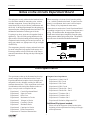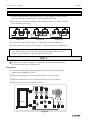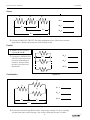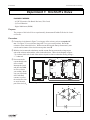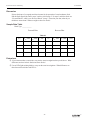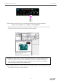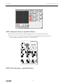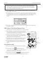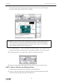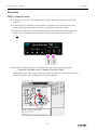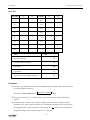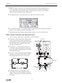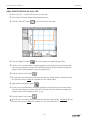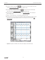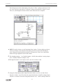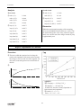
1
Includes Teacher's Notes and Typical Experiment Results Instruction Manual and Experiment Guide for the PASCO scientific Model EM-8656 012-05892A 1/96 AC/DC ELECTRONICS LABORATORY © 1995 PASCO scientific $15.00 012-05892A AC/DC Electronics Laboratory Table of Contents Section ...........................................................................................................Page Copyright, Warranty, and Equipment Return ................................................. ii Introduction ..................................................................................................... 1 Equipment ........................................................................................................ 1 Getting Started ................................................................................................. 2 Notes on the Circuits Experiment Board ......................................................... 3 The Experiments .............................................................................................. 4 Comments on Meters ....................................................................................... 4 Experiments Experiment 1: Circuits Experiment Board ....................................... 5 Experiment 2: Lights in Circuits ...................................................... 7 Experiment 3: Ohm's Law ................................................................ 9 Experiment 4: Resistances in Circuits ............................................ 11 Experiment 5: Voltages in Circuits ................................................ 15 Experiment 6: Currents in Circuits ................................................. 19 Experiment 7: Kirchhoff's Rules .................................................... 21 Experiment 8: Capacitors in Circuits.............................................. 23 Experiment 9: Diodes ..................................................................... 25 Experiment 10: Transistors ............................................................... 27 Computer Experiments Experiment 11: Ohm’s Law II .......................................................... 29 Experiment 12: RC Circuit ............................................................... 37 Experiment 13: LR Circuit ............................................................... 43 Experiment 14: LRC Circuit............................................................. 49 Experiment 15: Diode Lab – Part 1 .................................................. 57 Experiment 16: Diode Lab – Part 1 .................................................. 67 Experiment 17: Transistor Lab 1 – The NPN Transistor as a Digital Switch .......................................................................... 85 Experiment 18: Transistor Lab 2 – Current Gain: The NPN Emitter-Follower Amplifier .......................................... 93 Experiment 19: Transistor Lab 3 – Common Emitter Amplifier ... 101 Experiment 20: Induction – Magnet Through a Coil ..................... 109 Appendix: Tips and Troubleshooting ......................................................... 113 Teacher's Guide ........................................................................................... 115 Technical Support ................................................................................ Back Cover ® i AC/DC Electronics Laboratory 012-05892A Copyright, Warranty and Equipment Return Please—Feel free to duplicate this manual subject to the copyright restrictions below. Copyright Notice Equipment Return The PASCO scientific Model EM-8656 AC/DC Electronics Laboratory manual is copyrighted and all rights reserved. However, permission is granted to non-profit educational institutions for reproduction of any part of this manual providing the reproductions are used only for their laboratories and are not sold for profit. Reproduction under any other circumstances, without the written consent of PASCO scientific, is prohibited. Should the product have to be returned to PASCO scientific for any reason, notify PASCO scientific by letter, phone, or fax BEFORE returning the product. Upon notification, the return authorization and shipping instructions will be promptly issued. NOTE: NO EQUIPMENT WILL BE ACCEPTED FOR RETURN WITHOUT AN AUTHORIZATION FROM PASCO. ä Limited Warranty PASCO scientific warrants this product to be free from defects in materials and workmanship for a period of one year from the date of shipment to the customer. PASCO will repair or replace, at its option, any part of the product which is deemed to be defective in material or workmanship. This warranty does not cover damage to the product caused by abuse or improper use. Determination of whether a product failure is the result of a manufacturing defect or improper use by the customer shall be made solely by PASCO scientific. Responsibility for the return of equipment for warranty repair belongs to the customer. Equipment must be properly packed to prevent damage and shipped postage or freight prepaid. (Damage caused by improper packing of the equipment for return shipment will not be covered by the warranty.) Shipping costs for returning the equipment, after repair, will be paid by PASCO scientific. When returning equipment for repair, the units must be packed properly. Carriers will not accept responsibility for damage caused by improper packing. To be certain the unit will not be damaged in shipment, observe the following rules: ➀ The packing carton must be strong enough for the item shipped. ➁ Make certain there are at least two inches of packing material between any point on the apparatus and the inside walls of the carton. ➂ Make certain that the packing material cannot shift in the box or become compressed, allowing the instrument come in contact with the packing carton. Credits This manual authored by: Ann Hanks and Dave Griffith ii Address: PASCO scientific 10101 Foothills Blvd. Roseville, CA 95747-7100 Phone: FAX: email: web: (916) 786-3800 (916) 786-3292 [email protected] www.pasco.com ® 012-05892A AC/DC Electronics Laboratory Introduction The EM-8656 AC/DC Electronics Laboratory is designed for both DC and AC electricity experiments. The circuit board can be powered by batteries for DC experiments or it can be powered by a computer equipped with a Power Amplifier for AC experiments. The AC experiments could also be performed without a Power Amplifier if a function generator is available. The first ten experiments in this manual are DC experiments using battery power and multimeters rather than using a computer. The rest of the experiments use a computer (MAC or PC) with a Power Amplifier. The software used is Science Workshop™. Equipment The PASCO Model EM-8656 AC/DC Electronics Laboratory includes the following materials: The Component Bag includes: Resistors, 5% • Circuits Experiment Board • Storage Case • Component Bag • Experiment Manual (1) (2) (2) (2) (4) (2) (4) (2) (1) (1) (2) (1) Capacitors The Circuit Experiment Board features: (1) 1 µF–– 35 volts (2) 10 µF–– 25 volts (1) 47 µF–– 50 volts (1) 470 µF–– 16 volts (1) 100 µF–– 16 volts (1) 330 µF–– 16 volts (2) Battery Holders, D-cell, (Batteries not included) (3) Light Sockets (3) #14 Light Bulbs – 2.5 V, 0.3 A* (1) Transistor Socket (1) Coil (Renco RL-1238-8200) (1) Resistor–– 3.3 Ω, 2W, 5% (36) Component springs (2) Banana Jacks (for power amplifier) (1) Potentiometer–– 25 Ω, 2W (1) Pushbutton switch The Storage Case features: (6) Diodes 1N-4007 (2) Transistors 2N-3904 (1 ea) LED red, green, yellow, bicolor Wire Leads––22 ga. (4@5" and 5 @10") * NOTE: Due to manufacturer's tolerances, wattage may vary by 15-30% from bulb to bulb. (1) Cable clamp and 1/2" iron core ® 33 Ω–– 5 watt 10 Ω–– 1 watt 4.7 Ω–– 1/2 watt 100 Ω–– 1/2 watt 330 Ω–– 1/2 watt 560 Ω–– 1/2 watt 1 KΩ–– 1/2 watt 10 KΩ–– 1/2 watt 100 KΩ–– 1/2 watt 220 ΚΩ–– 1/2 watt 22 KΩ–– 1/4 watt 3.3 KΩ–– 1/4 watt 1 AC/DC Electronics Laboratory 012-05892A Getting Started ➀ Store the components in the Ziplock bag until needed. ➃ Students will need to use the same component layout Keep track of, and return the components to the Ziplock bag after the experiment is completed. from one experiment to another. Labeling of the boards and your meters will enable students to more easily have continuity in their work. Using removable labels or using a permanent marker are two alternatives for marking the board. ➁ Identify the resistor value required for the individual experiments with the help of the following chart. ➂ Familiarize yourself with the board layout, as shown. Black Brown Red Orange Yellow Green Blue Violet Gray White 0 1 2 3 4 5 6 7 8 9 2nd Digit 1st Digit No. of Zeros Tolerance Fourth Band None ±20% Silver ±10% Gold ±5% Red ±2% Resistor Chart (3) Light Bulbs and Sockets Transistor socket 3.3Ω Resistor Potentiometer (for Iron core) 3 VOLT BULBS KIT NO. Pushbutton switch Coil + A B C 3.3Ω 3 VOLTS MAX – E C Battery Holder Component spring C W B + Banana Jacks – EM-8656 AC/DC ELECTRONICS LABORATORY Board Layout 2 ® 012-05892A AC/DC Electronics Laboratory Notes on the Circuits Experiment Board The springs are securely soldered to the board and serve as a convenient method for connecting wires, resistors and other components. Some of the springs are connected electrically to devices like the potentiometer and the D-cells. In the large Experimental Area, the springs are connected in pairs, oriented perpendicular to each other. This facilitates the connection of various types of circuits. When connecting a circuit to a D-cell, note the polarity (+ or -) which is printed on the board. In some cases the polarity is not important, but in some it will be imperative. Polarity is very important for most meters. Connections are made on the Circuits Experiment Board by pushing a stripped wire or a lead to a component into a spring. For maximum effect, the stripped part of the wire should extend so that it passes completely across the spring, making contact with the spring at four points. This produces the most secure electrical and mechanical connection. If a spring is too loose, press the coils together firmly to tighten it up. The coils of the spring should not be too tight, as this will lead to bending and/or breaking of the component leads when they are inserted or removed. If a spring gets pushed over, light pressure will get it straightened back up. Spring Wire The components, primarily resistors, and small wires can be stored in the plastic bag supplied in the storage case. Encourage students to keep careful track of the components and return them to the bag each day following the lab period. (top view) (side view) Figure 1 Diagram of wires and springs The Experiments The experiments written up in this manual are developmental, starting from an introduction to the Circuits Experiment Board and complete circuits, through series and parallel circuits, ultimately resulting in diode and transistor characteristics. These experiments can be used in combination with existing labs that the teacher employs, or may be used as a complete lab unit. Experiment 1 Experiment 2 Experiment 3 Experiment 4 Experiment 5 Experiment 6 Experiment 7 Experiment 8 Experiment 9 Experiment 10 ® Computer based experiments Experiment 11 Experiment 12 Experiment 13 Experiment 14 Experiment 15 Experiment 16 Experiment 17 Experiment 18 Experiment 19 Experiment 20 Circuits Experiment Board Lights in Circuits Ohm’s Law Resistances in Circuits Voltages in Circuits Currents in Circuits Kirchhoff’s Rules Capacitors in Circuits Diode Characteristics Transistor Characteristics Ohm's Law II RC Circuit LR Circuit LRC Circuit Diodes Lab – Part 1 Diodes Lab – Part 2 Transistor Lab 1 Transistor Lab 2 Transistor Lab 3 Induction, Magnet and Coil Additional Equipment needed: Please refer to the Equipment Needed section in the beginning of each experiment for a listing of all equipment requirements. 3 AC/DC Electronics Laboratory 012-05892A Comments on Meters VOM: VTVM: The Volt-Ohm-Meter or VOM is a multiple scale, multiple function meter (such as the PASCO SB-9623 Analog Multimeter), typically measuring voltage and resistance, and often current, too. These usually have a meter movement, and may select different functions and scales by means of a rotating switch on the front of the unit. The Vacuum Tube Voltmeter or VTVM is a multiple scale, multiple function meter, typically measuring voltage and resistance. They do not usually measure current. The meter is an analog one, with a variety of scales, selected with a rotating switch on the front of the meter. Advantages: VOM’s may exist in your laboratory and thus be readily accessible. A single meter may be used to make a variety of measurements rather than needing several meters. Advantages: VTVM’s have high input resistances, on the order of 106 Ω or greater. By measuring the voltage across a known resistance, current can be measured with a VTVM. Disadvantages: VOM’s may be difficult for beginning students to learn to read, having multiple scales corresponding to different settings. VOM’s are powered by batteries for their resistance function, and thus must be checked to insure the batteries are working well. Typically, VOM’s may have input resistances of 30,000 Ω on the lowest voltage range, the range that is most often used in these experiments. For resistances in excess of 1,000 Ω, this low meter resistance affects circuit operation during the taking of readings, and thus is not usable for the capacitor, diode and transistor labs. Disadvantages: VTVM’s have multiple scales. Students need practice to avoid the mistake of reading the incorrect one. An internal battery provides the current for measuring resistance, and needs to be replaced from time to time. Grounding problems can occur when using more than one VTVM to make multiple measurements in the same circuit. Panelmeters: Individual meters, frequently obtained from scientific supply houses, are available in the form of voltmeters, ammeters, and galvanometers (such as PASCO’s SE-9748 Voltmeter 5 V, 15 V , SE-9746 Ammeter 1 A, 5 A and SE-9749 Galvanometer ± 35 mV). In some models, multiple scales are also available. DMM: The Digital Multimeter or DMM is a multiple scale, multiple function meter (such as the PASCO SB-9624 Basic Digital Multimeter or the SE-9589 General Purpose DMM), typically measuring voltage and resistance, and often current, too. These have a digital readout, often with an LCD (Liquid Crystal Display). Different functions and scales are selected with either a rotating switch or with a series of pushbutton switches. Advantages: Meters can be used which have the specific range required in a specific experiment. This helps to overcome student errors in reading. Disadvantages: Using individual meters leads to errors in choosing the correct one. With limited ranges, students may find themselves needing to use another range and not have a meter of that range available. Many of the individual meters have low input impedances (voltmeters) and large internal resistances (ammeters). Ohmmeters are almost nonexistent in individual form. Advantages: DMM’s are easily read, and with their typically high input impedances (>106 Ω) give good results for circuits having high resistance. Students learn to read DMM’s quickly and make fewer errors reading values. Reasonable quality DMM’s can be purchased for $60 or less. PASCO strongly recommends the use of DMM’s. Light Bulbs Disadvantages: DMM’s also require the use of a battery, although the lifetime of an alkaline battery in a DMM is quite long. The battery is used on all scales and functions. Most DMM’s give the maximum reading on the selector (i.e., under voltage, “2” means 2-volt maximum, actually 1.99 volt maximum). This may be confusing to some students. The #14 bulbs are nominally rated at 2.5 V and 0.3 A. However, due to relatively large variations allowed by the manufacturer, the wattage of the bulbs may vary by 15 to 30%. Therefore, supposedly “identical” bulbs may not shine with equal brightness in simple circuits. 4 ® 012-05892A AC/DC Electronics Laboratory Experiment 1: Circuits Experiment Board EQUIPMENT NEEDED: – AC/DC Electronics Lab Board: Wire Leads – D-cell Battery – Graph Paper Purpose The purpose of this lab is to become familiar with the Circuits Experiment Board, to learn how to construct a complete electrical circuit, and to learn how to represent electrical circuits with circuit diagrams. Background ➀ Many of the key elements of electrical circuits have been reduced to symbol form. Each symbol represents an element of the device’s operation, and may have some historical significance. In this lab and the ones which follow, we will use symbols frequently, and it is necessary you learn several of those symbols. Wire Switch Battery (Cell) Light Resistor Fuse ➁ The Circuits Experiment Board has been designed to conduct a wide variety of experiments easily and quickly. A labeled pictorial diagram of the Experiment Board appears on page 2. Refer to that page whenever you fail to understand a direction which mentions a device on the board itself. ➂ Notes on the Circuits Experiment Board: a) The springs are soldered to the board to serve as convenient places for connecting wires, resistors and other components. Some of the springs are connected electrically to devices like the potentiometer and the D-cells. b) If a spring is too loose, press the coils together firmly to enable it to hold a wire more tightly. If a spring gets pushed over, light pressure will get it straightened back up. If you find a spring which doesn’t work well for you, please notify your instructor. c) The components, primarily resistors, are contained in a plastic case at the top of the board. Keep careful track of the components and return them to the storage bag following each lab period. This way you will get components with consistent values from lab to lab. d) When you connect a circuit to a D-cell (each “battery” is just a cell, with two or more cells comprising a battery) note the polarity (+ or -) which is printed on the board. Although in some cases the polarity may not be important, in others it may very important. e) Due to normal differences between light bulbs, the brightness of “identical” bulbs may vary substantially. ® 5 AC/DC Electronics Laboratory 012-05892A Procedure ➀ Use two pieces of wire to make connections between the springs on one of the light bulbs to the springs on the D-cell in such a way that the light will glow. Discuss with your lab partner before you begin actually wiring your circuit which connections you intend to make, and why you think you will be successful in activating the light. If you are not successful, try in order: changing the wiring, using another light, using another cell, asking the instructor for assistance. a) Sketch the connections that the wires make when you are successful, using the symbols from the first page of this lab. b) Re-sketch the total circuit that you have constructed, making the wires run horizontally and vertically on the page. This is more standard in terms of drawing electrical circuits. ➁ Reverse the two wires at the light. Does this have any effect on the operation? Reverse the two wires at the cell. Does this have any effect on the operation? ➂ In the following steps, use the pushbutton switch as A + shown on the right. ➃ Use additional wires as needed to connect a second light into the circuit in such a way that it is also lighted. (Use the switch to turn the power on and off once the complete wiring has been achieved.) Discuss your plans with your lab partner before you begin. Once you have achieved success, sketch the connections that you made in the form of a circuit diagram. Annotate your circuit diagram by making appropriate notes to the side indicating what happened with that particular circuit. If you experience lack of success, keep trying. Battery – Switch Figure 1.1 ➤ NOTE: Is your original light the same brightness, or was it brighter or dimmer that it was during step 1? Can you explain any differences in the brightness, or the fact that it is the same? If not, don’t be too surprised, as this will be the subject of future study. ➄ If you can devise another way of connecting two lights into the same circuit, try it out. Sketch the circuit diagram when finished and note the relative brightness. Compare your brightness with what you achieved with a single light by itself. ➅ Disconnect the wires and return them to the plastic bag. Replace the equipment to its storage case. 6 ® 012-05892A AC/DC Electronics Laboratory Experiment 2: Lights in Circuits EQUIPMENT NEEDED: – AC/DC Electronics Lab Board: Wire Leads – (2) D-cell Batteries – Graph Paper Purpose The purpose of this lab is to determine how light bulbs behave in different circuit arrangements. Different ways of connecting two batteries will also be investigated. Procedure PART A ➤ NOTE: Due to variations from bulb to bulb, the brightness of one bulb may be substantially different from the brightness of another bulb in “identical” situations. ➀ Use two pieces of wire to connect a single light bulb to one of the D-cells in such a way that the light will glow. Include a “switch” to turn the light on and off, preventing it from being on continuously. (You should have completed this step in Experiment 1. If that is the case, review what you did then. If not, continue with this step.) ➁ Use additional wires as needed to connect a second light into the circuit in such a way that it is also lighted. Discuss your plans with your lab partner before you begin. Once you have achieved success, sketch the connections that you made in the form of a circuit diagram using standard symbols. Annotate your circuit diagram by making appropriate notes to the side indicating what happened with that particular circuit. ➤ NOTE: Is your original light the same brightness, or was it brighter or dimmer than it was during step 1? Can you explain any differences in the brightness, or why it is the same? ➂ If one of the light bulbs is unscrewed, does the other bulb go out or does it stay on? Why or why not? ➃ Design a circuit that will allow you to light all three lights, with each one being equally bright. Draw the circuit diagram once you have been successful. If you could characterize the circuit as being a series or parallel circuit, which would it be? What happens if you unscrew one of the bulbs? Explain. ➄ Design another circuit which will also light all three bulbs, but with the bulbs all being equally bright, even though they may be brighter or dimmer than in step 4. Try it. When you are successful, draw the circuit diagram. What happens if you unscrew one of the bulbs? Explain. ➅ Devise a circuit which will light two bulbs at the same intensity, but the third at a different intensity. Try it. When successful, draw the circuit diagram. What happens if you unscrew one of the bulbs? Explain. ➤ NOTE: Are there any generalizations that you can state about different connections to a set of lights? ® 7 AC/DC Electronics Laboratory 012-05892A PART B ➆ Connect a single D-cell to a single light as in step 1, using a spring clip “switch” to allow you to easily turn the current on and off. Note the brightness of the light. ⑧ Now connect the second D-cell into the circuit as shown in Figure 2.1a. What is the effect on the brightness of the light? Figure 2.1b Figure 2.1a Figure 2.1c ⑨ Connect the second D-cell as in Figure 2.1b. What is the effect on the brightness? ➉ Finally, connect the second D-cell as in figure 2.1c. What is the effect on the brightness? ➤ NOTE: Determine the nature of the connections between the D-cells you made in steps 8-10. Which of these was most useful in making the light brighter? Which was least useful? Can you determine a reason why each behaved as it did? PART C 11 Connect the circuit shown in Figure 2.2. What is the effect of rotating the knob on the device that is identified as a “Potentiometer?” Discussion ➀ Answer the questions which appear during the experiment procedure. Pay particular attention to the “NOTED:” questions. ➁ What are the apparent rules for the operation of lights in series? In parallel? ➂ What are the apparent rules for the operation of batteries in series? In parallel? ➃ What is one function of a potentiometer in a circuit? + Battery – A B C E C C W B Figure 2.2 8 ® 012-05892A AC/DC Electronics Laboratory Experiment 3: Ohm’s Law EQUIPMENT NEEDED: – AC/DC Electronics Lab Board: Wire Leads – D-cell Battery – Multimeter – Graph Paper Purpose The purpose of this lab will be to investigate the three variables involved in a mathematical relationship known as Ohm’s Law. Procedure ➀ Choose one of the resistors that you have been given. Using the chart on the next page, decode the resistance value and record that value in the first column of Table 3.1. ➁ MEASURING CURRENT: Construct the circuit shown in Figure 3.1a by pressing the leads of the resistor into two of the springs in the Experimental Section on the Circuits Experiment Board. Red (+) Black (-) Black (-) Red (+) + Battery + – Battery – Figure 3.1b Figure 3.1a ➂ Set the Multimeter to the 200 mA range, noting any special connections needed for measuring current. Connect the circuit and read the current that is flowing through the resistor. Record this value in the second column of Table 3.1. ➃ Remove the resistor and choose another. Record its resistance value in Table 3.1 then measure and record the current as in steps 2 and 3. Continue this process until you have completed all of the resistors you have been given. As you have more than one resistor with the same value, keep them in order as you will use them again in the next steps. ➄ MEASURING VOLTAGE: Disconnect the Multimeter and connect a wire from the positive lead (spring) of the battery directly to the first resistor you used as shown in Figure 3.1b. Change the Multimeter to the 2 VDC scale and connect the leads as shown also in Figure 3.1b. Measure the voltage across the resistor and record it in Table 3.1. ➅ Remove the resistor and choose the next one you used. Record its voltage in Table 3.1 as in step 5. Continue this process until you have completed all of the resistors. ® 9 AC/DC Electronics Laboratory 012-05892A Data Processing ➀ Construct a graph of Current (vertical axis) vs Resistance. ➁ For each of your sets of data, calculate the ratio of Voltage/Resistance. Compare the values you calculate with the measured values of the current. Table 3.1 Resistance, Ω Current, amp Voltage, volt Voltage/Resistance Discussion ➀ From your graph, what is the mathematical relationship between Current and Resistance? ➁ Ohm’s Law states that current is given by the ratio of voltage/resistance. Does your data concur with this? ➂ What were possible sources of experimental error in this lab? Would you expect each to make your results larger or to make them smaller? Reference Black Brown Red Orange Yellow Green Blue Violet Gray White 0 1 2 3 4 5 6 7 8 9 2nd Digit 1st Digit No. of Zeros Tolerance 10 Fourth Band None ±20% Silver ±10% Gold ±5% Red ±2% ® 012-05892A AC/DC Electronics Laboratory Experiment 4: Resistances in Circuits EQUIPMENT NEEDED: – AC/DC Electronics Lab Board: Resistors – Multimeter Purpose The purpose of this lab is to begin experimenting with the variables that contribute to the operation of an electrical circuit. This is the first of a three connected labs. Procedure ➀ Choose three resistors of the same value. Enter those sets of colors in Table 4.1 below. We will refer to one as #1, another as #2 and the third as #3. ➁ Determine the coded value of your resistors. Enter the value in the column labeled “Coded Resistance” in Table 4.1. Enter the Tolerance value as indicated by the color of the fourth band under “Tolerance.” ➂ Use the Multimeter to measure the resistance of each of your three resistors. Enter these values in Table 4.1. ➃ Determine the percentage experimental error of each resistance value and enter it in the appropriate column. Experimental Error = [(|Measured - Coded|) / Coded ] x 100%. Table 4.1 1st Colors 2nd 3rd Coded Measured 4th Resistance Resistance % Error Tolerance #1 #2 #3 ➄ Now connect the three resistors into the SERIES CIRCUIT, figure 4.1, using the spring clips on the Circuits Experiment Board to hold the leads of the resistors together without bending them. Measure the resistances of the combinations as indicated on the diagram by connecting the leads of the Multimeter between the points at the ends of the arrows. ® 11 AC/DC Electronics Laboratory 012-05892A Series R1 R2 R3 R12= R23= ➤ R12 ➤ ➤ ➤ R23 R123= ➤ ➤ R123 Figure 4.1 ➅ Construct a PARALLEL CIRCUIT, first using combinations of two of the resistors, and then using all three. Measure and record your values for these circuits. Parallel R1 ➤ NOTE: Include also R13 by replacing R2 with R3. ➤ ➆ Connect the COMBINATION CIRCUIT below and measure the various combinations of resistance. Do these follow the rules as you discovered them before? R12 = ➤ R12 R23 = R2 R123 = R3 Combination Figure 4.2 R2 R1 R1 = R3 R23 = ➤ ➤ R1 R123 R2 3 ➤ ➤ R123 = ➤ Figure 4.3 ⑧ Choose three resistors having different values. Repeat steps 1 through 7 as above, recording your data in the spaces on the next page. Note we have called these resistors A, B and C. 12 ® 012-05892A AC/DC Electronics Laboratory Table 4.2 Colors 2nd 3rd 1st Coded Measured 4th Resistance Resistance % Error A B C Series RA RB RC RAB = RAB RBC = ➤ RBC ➤ ➤ RABC ➤ ➤ ➤ Figure 4.4 Parallel RA RAB RAB = ➤ ➤ RBC = RB RABC= RC Figure 4.5 ➤ NOTE: Include also RAC by replacing RB with RC. ® 13 RABC= Tolerance AC/DC Electronics Laboratory 012-05892A Combination RB RA RA = RC RBC = ➤ ➤ RA ➤ ➤ RBC RABC RABC= ➤ Figure 4.6 Discussion ➀ How does the % error compare to the coded tolerance for your resistors? ➁ What is the apparent rule for combining equal resistances in series circuits? In parallel circuits? Cite evidence from your data to support your conclusions. ➂ What is the apparent rule for combining unequal resistances in series circuits? In parallel circuits? Cite evidence from your data to support your conclusions. ➃ What is the apparent rule for the total resistance when resistors are added up in series? In parallel? Cite evidence from your data to support your conclusions. Extension Using the same resistance values as you used before plus any wires needed to help build the circuit, design and test the resistance values for another combination of three resistors. As instructed, build circuits with four and five resistors, testing the basic concepts you discovered in this lab. Reference Black Brown Red Orange Yellow Green Blue Violet Gray White 0 1 2 3 4 5 6 7 8 9 2nd Digit 1st Digit No. of Zeros Tolerance Fourth Band None ±20% Silver ±10% Gold ±5% Red ±2% Figure 4.7 14 ® 012-05892A AC/DC Electronics Laboratory Experiment 5: Voltages in Circuits EQUIPMENT NEEDED: – AC/DC Electronics Lab Board: Wire Leads, Resistors – D-cell Battery – Multimeter Purpose The purpose of this lab will be to continue experimenting with the variables that contribute to the operation of an electrical circuit. You should have completed Experiment 4 before working on this lab. Procedure ➀ Connect the three equal resistors that you used in Experiment 4 into the series circuit shown below, using the springs to hold the leads of the resistors together without bending them. Connect two wires to the D-cell, carefully noting which wire is connected to the negative and which is connected to the positive. ➁ Now use the voltage function on the Multimeter to measure the voltages across the individual resistors and then across the combinations of resistors. Be careful to observe the polarity of the leads (red is +, black is -). Record your readings below. Series + - V1 + R3 R2 R1 ➤ ➤ - + + - ➤ V12 ➤ ➤ V23 V123 ➤ Figure 5.1 ® + - R1 = V1 = R2 = V2 = R3 = V3 = R12 = V12 = R23 = V23 = R123= V123= 15 ➤ ➤ AC/DC Electronics Laboratory 012-05892A ➂ Now connect the parallel circuit below, using all three resistors. Measure the voltage across each of the resistors and the combination, taking care with the polarity as before. ➤ NOTE: Keep all three resistors connected throughout the time you are making your measurements. Write down your values as indicated below. Parallel + - ➤ ➤ R1 R1 = V1 = R2 = V2 = R3 = V3 = R123 = V123 = V1 R2 R3 Figure 5.2 ➃ Now connect the circuit below and measure the voltages. You can use the resistance readings you took in Experiment 4 for this step. Combination + - R2 R1 R1 = V1 = R23 = V23 = R123 = V123 = R3 ➤ ➤ V1 V123 V23 ➤ ➤ ➤ ➤ Figure 5.3 ➄ Use the three unequal resistors that you used in Experiment 4 to construct the circuits shown below. Make the same voltage measurements that you were asked to make before in steps 1 to 4. Use the same resistors for A, B and C that you used in Experiment 4. 16 ® 012-05892A AC/DC Electronics Laboratory Series + - VA + RA RC RB - + - + - + ➤ ➤ VAB ➤ VBC VABC ➤ ➤ ➤ Figure 5.4 RA = VA = RB = VB = RC = VC = RAB = VAB = RBC = VBC = RABC= VABC= Parallel + - ➤ ➤ RA VA RB RA = VA = RB = VB = RC = VC = RABC= VABC= RC Figure 5.5 ® 17 AC/DC Electronics Laboratory 012-05892A Combination + - RA = VA = RBC = VBC = RABC= VABC = RB RA RC ➤ VA ➤ VABC VBC ➤ ➤ ➤ ➤ Figure 5.6 Discussion On the basis of the data you recorded on the table with Figure 5.1, what is the pattern for how voltage gets distributed in a series circuit with equal resistances? According to the data you recorded with Figure 5.4, what is the pattern for how voltage gets distributed in a series circuit with unequal resistances? Is there any relationship between the size of the resistance and the size of the resulting voltage? Utilizing the data from Figure 5.2, what is the pattern for how voltage distributes itself in a parallel circuit for equal resistances? Based on the data from Figure 5.5, what is the pattern for how voltage distributes itself in a parallel circuit for unequal resistances? Is there any relationship between the size of the resistance and the size of the resulting voltage? Do the voltages in your combination circuits (see Figures 5.3 and 5.6) follow the same rules as they did in your circuits which were purely series or parallel? If not, state the rules you see in operation. 18 ® 012-05892A AC/DC Electronics Laboratory Experiment 6: Currents in Circuits EQUIPMENT NEEDED: – AC/DC Electronics Lab Board: Resistors and Wire Leads – D-cell Battery – Digital Multimeter Purpose The purpose of this lab will be to continue experimenting with the variables that contribute to the operation of electrical circuits. Procedure ➀ Connect the same three resistors that you used in Experiments 3 and 4 into the series circuit shown below, using the springs to hold the leads of the resistors together without bending them. Connect two wires to the D-cell, and carefully note which lead is negative and which is positive. Series ➁ Now change the leads in your DMM so that they can be used to measure current. You should be using the scale which goes to a maximum of 200 mA. Be careful to observe the polarity of the leads (red is +, black is -). In order to measure current, the circuit must be interrupted, and the current allowed to flow through the meter. Disconnect the lead wire from the positive terminal of the battery and connect it to the red (+) lead of the meter. Connect the black (-) lead to R1, where the wire originally was connected. Record your reading in the table as Io. See Figure 6.2. ➂ Now move the DMM to the positions indicated in Figure 6.3, each time interrupting the circuit, and carefully measuring the current in each one. Complete the table on the top of the back page. + R1 - R2 + R3 - + - + Figure 6.1 - I0 + + R1 + R3 R2 - + - Figure 6.2 ➤ NOTE: You will be carrying values from Experiments 3 and 4 into the table on the back. ® - 19 + - AC/DC Electronics Laboratory 012-05892A - I0 + + - R1 - + I2 R3 R2 + I1 + - I3 - Figure 6.3 R1 = I0 = V1 = R2 = I1 = V2 = R3 = I2 = V3 = R12 = I3 = V12 = R23 = V23 = R123= V123= ➃ Connect the parallel circuit below, using all three resistors. Review the instructions for connecting the DMM as an ammeter in step 2. Connect it first between the positive terminal of the battery and the parallel circuit junction to measure I0. Then interrupt the various branches of the parallel circuit and measure the individual branch currents. Record your measurements in the table below. Parallel R1 I0 = = + V1 = R2 = I1 = V2 R3 = I2 = V3 = I3 = R123 = - + - I0 = - I4 R1 + I1 - + I2 - + I3 - + R2 V123 = R3 I4 = Figure 6.4 Discussion On the basis of your first set of data, what is the pattern for how current behaves in a series circuit? At this point you should be able to summarize the behavior of all three quantities resistance, voltage and current - in series circuits. On the basis of your second set of data, are there any patterns to the way that currents behave in a parallel circuit? At this time you should be able to write the general characteristics of currents, voltages and resistances in parallel circuits. 20 ® 012-05892A AC/DC Electronics Laboratory Experiment 7: Kirchhoff’s Rules EQUIPMENT NEEDED: – AC/DC Electronics Lab Board: Resistors, Wire Leads – (2) D-cell Batteries – Digital Multimeter (DMM) Purpose The purpose of this lab will be to experimentally demonstrate Kirchhoff’s Rules for electrical circuits. Procedure ➀ Connect the circuit shown in Figure 7.1a using any of the resistors you have except the 10 Ω one. Use Figure 7.1b as a reference along with 7.1a as you record your data. Record the resistance values in the table below. With no current flowing (the battery disconnected), measure the total resistance of the circuit between points A and B. ➁ With the circuit connected to the battery and the current flowing, measure the voltage across each of the resistors and record the values in the table below. On the circuit diagram in Figure 7.1b, indicate which side of each of the resistors is positive relative to the other end by placing a “+” at that end. A ➂ Now measure the current through each of the resistors. Interrupt the circuit and place the DMM in series to obtain your reading. Make sure you record each of the individual currents, as well as the current flow into or out of the main part of the circuit, IT. R2 B R1 + R5 Wire Battery – Wire R3 R4 D Figure 7.1a R1 C A R2 R4 D Figure 7.1b 21 B R5 R3 ® C AC/DC Electronics Laboratory 012-05892A Table 7.1 Resistance, Ω Voltage, volts Current, mA R1 V1 I1 R2 V2 I2 R3 V3 I3 R4 V4 I4 R5 V5 I5 RT VT IT Analysis ➀ Determine the net current flow into or out of each of the four “nodes” in the circuit. ➁ Determine the net voltage drop around at least three (3) of the six or so closed loops. Remember, if the potential goes up, treat the voltage drop as positive (+), while if the potential goes down, treat it as negative (-). Discussion Use your experimental results to analyze the circuit you built in terms of Kirchhoff’s Rules. Be specific and state the evidence for your conclusions. Extension Build the circuit below and apply the same procedure you used previously. Analyze it in terms of Kirchhoff’s Rules. If possible, try to analyze the circuit ahead of time and compare your measured values with the theoretically computed values. R2 R4 R3 R1 V2 R5 V1 Figure 7.2 22 ® 012-05892A AC/DC Electronics Laboratory Experiment 8: Capacitors in Circuits EQUIPMENT NEEDED: – AC/DC Electronics Lab Board: Capacitors, Resistors, Wire Leads – D-cell Battery – Stopwatch or timer with 0.1 sec resolution. – Vacuum Tube Voltmeter (VTVM) or Electrometer (ES-9054B) or Digital Multimeter (DMM) that has an input impedance of 10 MΩ or greater. Purpose The purpose of this lab will be to determine how capacitors behave in R-C circuits. The manner in which capacitors combine will also be studied. Procedure ➀ Connect the circuit shown in Figure 8.1, using a 100 kΩ resistor and a 100 µF capacitor. Connect the circuit as shown in Figure 8.1. Connect the VTVM so the black “ground” lead is on the side of the capacitor that connects to the negative terminal of the battery and set it so that it reads to a maximum of 1.5 V DC. ➁ Start with no voltage on the capacitor Battery and the switch off. If there is remaining voltage on the capacitor, use a piece of wire to “short” the two leads together, draining any remaining charge. (Touch the ends of the wire to points B and C as shown in Figure 8.1 to discharge the capacitor.) 3 VOLTS MAX – C C W - + V ➂ Now close the switch by pushing and holding the button down. Observe the voltage readings on the VTVM, the voltage across the capacitor. How would you describe the manner in which the voltage changes? E Switch + C Battery – B A Cap Res Figure 8.1 ➃ If you now open the switch by releasing the button, the capacitor should remain at its present voltage with a very slow drop over time. This indicates that the charge you placed on the capacitor has no way to move back to neutralize the excess charges on the two plates. ➄ Connect a wire between points A and C in the circuit, allowing the charge to drain back through the resistor. Observe the voltage readings on the VTVM as the charge flows back. How would you describe the manner in which the voltage falls? (It would be reasonable to sketch a graph showing the manner in which the voltage rose over time as well as the manner in which it fell over time.) ➅ Repeat steps 3-5 until you have a good feeling for the process of charging and discharging of a capacitor through a resistance. ➆ Now repeat steps 3-5, this time recording the time taken to move from 0.0 volts to 0.95 volts while charging, tC, and the time taken to move from 1.5 volts to 0.55 volts while discharging, tD. Record your times along with the resistance and capacitance values in Table 8.1 at the top of the back page. ® 23 AC/DC Electronics Laboratory 012-05892A Table 8.1 Trial Resistance Capacitance tC tD 1 2 3 4 5 6 7 8 ⑧ Replace the 100 µF capacitor with a 330 µF capacitor. Repeat step 7, recording the charging and discharging times in Table 8.1. If a third value is available, include it in the data table, too. ⑨ Return to the original 100 µF capacitor, but put a 220 kΩ resistor in the circuit. Repeat step 7, recording your data in Table 8.1. If a third resistor is provided, use it in the circuit, recording the data. ➤ NOTE: ➀ What is the effect on charging and discharging times if the capacitance is increased? What mathematical relationship exists between your times and the capacitance? ➁ What is the effect on charging and discharging times if the resistance of the circuit is increased? What mathematical relationship exists between your times and the resistance? ➉ Return to the original 100 kΩ resistor, but use the 100 µF capacitor in series with the 330 µF capacitor. Repeat step 7, recording your results in Table 8.2. 11 Now repeat step 7, but with the 100 µF and the 330 µF capacitors in parallel. R = __________ C1 = __________C2 = __________ Table 8.2 Type of Circuit tC tD Series Parallel ➤ NOTE: What is the effect on the total capacitance if capacitors are combined in series? What if they are combined in parallel? (Refer to Table 8.2). 24 ® 012-05892A AC/DC Electronics Laboratory Experiment 9: Diodes EQUIPMENT NEEDED: – AC/DC Electronics Lab Board: 1 KΩ Resistor, 330 Ω Resistor, 1N4007 Diode, Wire Leads – Digital Multimeter (DMM) – (2) D-cell Batteries Purpose The purpose of this lab will be to experimentally determine some of the operating characteristics of semiconductor diodes. Procedure À Connect the circuit shown in Figure 9.1a using the 1N4007 diode you’ve been supplied and the 1 KΩ resistor. Use Figure 9.1b as a reference along with Figure 9.1a as you record your data. Note the direction that the diode is oriented, with the dark band closer to point B. + Battery – C W Switch Á With the “switch” closed and the current flowing, adjust the potentiometer until there is a voltage of 0.05 volt between points B and C (VBC). Measure the voltage across the diode (VAB). Record your values in the left-hand side of Table 9.1 under “Forward Bias”. + C Battery A B – Diode Res  Adjust the potentiometer to attain the following values for VBC: 0.1, 0.2, 0.3,.....2.0 volts. Record the two voltages for each case. Figure 9.1a à Remove the 1 KΩ resistor and replace it with a 330-Ω resistor. Repeat steps 3 & 4, going from a voltage of 0.3, 0.4,.....2.0 volts. Record VBC and VAB in each case. A Ä Reverse the orientation of the diode. Set the diode voltage 1N4007 (VAB) to the values 0.5, 1.0,....3.0 volts. Measure the resistor voltage (VBC) in each case. Record these values in the columns labeled “Reverse Bias”. Analysis C R Figure 9.1b À Determine the current flow (I) in each setting by dividing the voltage across the resistor (VBC) by the resistance. Where you switched resistors, be sure to change the divisor. Á Construct a graph of Current (vertical axis) vs the Voltage across the diode, with the graph extending into the 2nd quadrant to encompass the negative voltages on the diode. ® 25 B AC/DC Electronics Laboratory 012-05892A Discussion Discuss the shape of your graph and what it means for the operation of a semiconductor diode. Did the diode operate the same in steps 3 and 4 as it did in step 5? In steps 3 and 4 the diode was “Forward Biased”, while it was “Reverse Biased” in step 5. Based on your data, what do you think these terms mean? What use might we have for diodes? Sample Data Table Diode Type ____________ Forward Bias Reverse Bias Table 9.1 R, Ω VAB, volts VBC, volts R, Ω I, mA VAB, volts VBC, volts I, mA Extensions ➀ If your instructor has a zener diode, carry out the same investigations that you did above. What differences are there in basic diodes and zener diodes? ➁ Use an LED (light emitting diode) to carry out the same investigations. What differences are there between basic diodes and LED’s? 26 ® 012-05892A AC/DC Electronics Laboratory Experiment 10: Transistors EQUIPMENT NEEDED: – AC/DC Electronics Lab Board: 1 kW Resistor, 100 Ω Resistor, 2N3904 Transistor (NPN), Wire Leads – (2) D-cell Batteries – Digital Multimeter (DMM) – Optional: additional Digital Multimeter Purpose The purpose of this lab will be to experimentally determine some of the operating characteristics of a transistor. Procedure ➀ Connect the circuit shown in Figure 10.1a using the 2N3904 Transistor you’ve been supplied. Resistor R1 = 1 K Ω and resistor R2 = 100 Ω. Use Figure 10.1b as a reference along with Figure 10.1a as you record your data. Note the leads on the transistor as marked next to the socket in the drawing. Transistor, top view e + c 2N3904 Battery – E C B C W R1 B D R2 Socket b 2N3904 ➤ CAUTION: Connecting the transistor incorrectly can destroy the transistor. A R2 C + C c R1 Battery A – Figure 10.1a b B Figure 10.1b ➁ Adjust the potentiometer carefully until the reading between points A and B is approximately 0.002 volt (2.0 mv). Now read the voltage between points C and D. Record these readings in your data table. Note that VAB divided by R1 gives the current flowing to the base of the transistor, while VCD divided by R2 gives the current flowing in the collector part of the circuit. ➂ Adjust the potentiometer to give VAB the following readings, each time reading and recording the corresponding VCD: 0.006, 0.010, 0.015, 0.020, 0.025, 0.030, 0.035, 0.040, 0.045, 0.050, 0.055, 0.060, 0.080, 0.100, 0.150, 0.200, 0.250 volts. Also set VAB to 0.000 volts. ® e 27 D AC/DC Electronics Laboratory 012-05892A Analysis ➀ For each of your sets of readings, calculate: IB = VAB / R1 and IC = VCD / R2 Record all of your current readings in mA. ➁ Plot a graph of IC (vertical axis) vs IB. If you find an area or areas where you need more points to fill out any curves or sudden changes, simply return to step 2 and make the appropriate measurements. ➂ What is the general shape of the graph? Is there a straight-line region? Does it go through the origin? Why or why not? Relate the behavior of the transistor at the beginning of the graph to the behavior of the diode in Experiment 9. ➃ What does the leveling off of the graph indicate? Electronics people refer to the transistor as being “saturated”. How would you describe saturation based on your experiment? ➄ Find the slope of the straight-line region of the graph. This ratio - I C / I B is referred to as the current amplification of the transistor. It describes how many times greater changes in the collector current are than the changes in the base current. Report the current amplification of your transistor. Discussion Discuss the graph and the calculations you did in the Analysis section. Sample Data Table Transistor Type ____________ Table 10.1 R1, Ω VAB, volts IB, mA R2, Ω VCD, volts IC, mA Extensions ➀ What effect would changing the resistance in the collector circuit (R2) make? Try changing the value to 330 Ω or 560 Ω. Does the graph have the same shape? Is the current amplification the same as before? How does the amplification depend on R2? ➁ Obtain a different transistor and repeat the measurements you made in steps 2 & 3. If it is a PNP transistor, you will need to reverse the wires coming from the D-cells as the emitter needs to be positive, not negative, and the collector will be negative. 28 ® 012-05892A AC/DC Electronics Laboratory Experiment 11: Ohm's Law II EQUIPMENT NEEDED: – Computer and Science Workshop™ Interface – Power Amplifier (CI-6552A) – AC/DC Electronics Lab Board (EM-8656): 10 Ω resistor, 3 V light bulb, and wire leads – (2) banana plug patch cords (such as SE-9750) Purpose The purpose of this experiment is to investigate the relationship between current and voltage in Ohmic and non-Ohmic materials. Theory Ohm discovered that when the voltage across a resistor changes, the current through the resistor changes. He expressed this as I = V/R (current is directly proportional to voltage and inversely proportional to resistance). In other words, as the voltage increases, so does the current. The proportionality constant is the value of the resistance. The current is INVERSELY proportional to the resistance. As the resistance increases, the current decreases. If the voltage across an “Ohmic” resistor is increased, the graph of voltage versus current shows a straight line (if the resistance remains constant). The slope of the line is the value of the resistance. However, if the resistance CHANGES (that is, if the resistor is “non-Ohmic”), the graph of voltage versus current will not be a straight line. Instead, it will show a curve with a changing slope. For a light bulb, the resistance of the filament will change as it heats up and cools down. At high AC frequencies, the filament doesn’t have time to cool down, so it remains at a nearly constant temperature and the resistance stays relatively constant. At low AC frequencies (e.g., less than one Hertz), the filament has time to change temperature. As a consequence, the resistance of the filament changes dramatically and the resulting change in current through the filament is interesting to watch. In the first part of this activity, you will investigate a ten ohm (Ω) resistor. In the second part, you will investigate the filament of a small light bulb. PROCEDURE Part A – Ten Ohm Resistor PART I: Computer Setup ➀ Connect the Science Workshop interface to the computer, turn on the interface, and turn on the computer. ➁ Plug the Power Amplifier into Analog Channel A. Plug the power cord into the back of the Power Amplifier and connect the power cord to an appropriate electrical receptacle ® 29 AC/DC Electronics Laboratory 012-05892A ➂ In the Physics Folder of the Science Workshop Experiment Library, open the document: Macintosh: “P46 Ohm's Law” / Windows: “P46_OHM.SWS” The document opens with a Scope (oscilloscope) display of Voltage (V) versus Current (A), and the Signal Generator window which controls the Power Amplifier. ➤ NOTE: For quick reference, see the Experiment Notes window. To bring a display to the top, click on its window or select the name of the display from the list at the end of the Display menu. Change the Experiment Setup window by clicking on the “Zoom” box or the Restore button in the upper right hand corner of that window. ➃ The “Sampling Options…” for this experiment are: Periodic Samples = Fast at 4000 Hz (set in the Scope display using the Sweep Speed control). 30 ® 012-05892A AC/DC Electronics Laboratory ➄ The Signal Generator is set to output 3.00 V, triangle AC waveform, at 60.00 Hz. ➅ The Scope is set to show Output Voltage on the vertical axis at 1.000 v/div and Current (Analog A) on the horizontal axis at 0.100 v/div. ➆ Arrange the Scope display and the Signal Generator window so you can see both of them. PART II: Sensor Calibration and Equipment Setup • You do not need to calibrate the Power Amplifier. ➀ Place a ten ohm (Ω) resistor in the pair of component springs KIT NO. nearest to the banana jacks at the lower right corner of the AC/DC Electronics Lab Board. ➁ Connect banana plug patch cords from the output of the Power Amplifier to the banana jacks on the AC/DC Electronics Lab Board. ➂ Turn on the power switch on the back of the Power Amplifier. 3 VOLTS MAX C W Part III: Data Recording – Resistor (10 Ω) ➀ Click the “ON” button ( ) in the Signal Generator to Power Amp. window. ➁ Click the “MON” button ( ) in the Experiment Setup window to start monitoring data. Observe the Scope display of Voltage and Current. Wait a few seconds, then click the “STOP” button ( 10Ω (brown, black, black) ). ➂ Click the “OFF” button ( ) in the Signal Generator window. Turn off the power switch on the back of the Power Amplifier. ® AC/DC ELECTRONICS LABORATORY 31 AC/DC Electronics Laboratory 012-05892A ➃ Select the Scope display. Analyzing the Data – Resistor (10 Ω) ➀ Click the “Smart Cursor” button ( ) in the Scope. The cursor changes to a cross-hair. Move the cursor into the display area of the Scope. • The Y-coordinate of the cursor/cross-hair is shown next to the Vertical Axis Input button: . • The X-coordinate of the cursor/cross-hair is shown next to the Horizontal Axis Input button: ➁ Use the coordinates of a point on the trace on the Scope display to determine the slope of the trace on the Scope. Record the value of the slope. 32 ® 012-05892A AC/DC Electronics Laboratory slope (10 Ω) = ________ Volts/Amps Optional ➀ Replace the 10 Ω resistor with the 100 Ω resistor. ➁ Click the “Increase Sweep Speed” button ( ) in the Scope display to change the sensitivity of the horizontal axis to 0.010 v/div. ➂ Repeat the experiment. Record the new slope. slope (100 Ω) = ________ Volts/Amps Part B – Light Bulb Filament PART I: Computer Setup for Light Bulb Filament For this part of the activity you will use the filament of a light bulb as the resistor. In the Computer Setup you will change the Amplitude and Frequency of the output AC waveform. You will also change some of the settings on the Scope display. ➀ Click the Signal Generator window to make it active. ➁ Click on the Amplitude value to highlight it. Type in “2.5” as the new value. Press the “enter” key. ® 33 AC/DC Electronics Laboratory 012-05892A ➂ Click on the Frequency value to highlight it. Type in “0.30” as the new value. Press the “enter” key. ➃ Click the Scope display to make it active. • You will change the rate at which the scope is sampling data. ➄ Click the “Horizontal Input” button. Use the Horizontal Input menu to select “Time Input” (at the bottom of the list). Horizontal Input button Horizontal Input menu ➅ Repeatedly click the “Decrease Sweep Speed” button ( ) until the Sweep Speed is 500.00 ms/div. ➄ Click the “Horizontal Input” button again. Use the Horizontal Input menu to select “Analog A” (at the top of the list). Horizontal Input button Horizontal Input menu • After making changes, the Scope display should be similar to the figure below: 34 ® 012-05892A AC/DC Electronics Laboratory PART II: Equipment Setup for Light Bulb Filament ➀ Remove the resistor from the component springs on the AC/DC Electronics Lab Board. ➁ Use two of the 10” wire leads to connect between the component springs near the banana jacks and the component springs above and below 3 VOLT BULB “C”. KIT NO. C 3.3Ω 3 VOLTS MAX C C W B EM-8656 AC/DC ELECTRONICS LABORATORY PART III: Data Recording – Light Bulb Filament ® 35 AC/DC Electronics Laboratory 012-05892A ➀ Turn on the switch on the back of the Power Amplifier. ➁ Click the “ON” button in the Signal Generator window. ➂ Click the “MON” button in the Experiment Setup window to begin monitoring data. Observe the Scope display of Voltage versus Current for the light bulb filament. ➃ Wait a few seconds, then click the “STOP” button. ➄ Click the “OFF” button in the Signal Generator window. Turn off the power switch on the back of the Power Amplifier. Questions ➀ Compare the slope of the 10 Ω resistor as shown in the Scope to the “official” value of resistance. In other words, how close is the value of slope to the value of resistance? ➁ Why does the slope of the light bulb trace change? ➂ Does the resistor have a constant resistance? Does the light bulb? Why or why not? ➃ The slope of the graph for the light bulb is not symmetric. Why is the slope of the current trace different when the filament is heating up compared to the trace of current when the filament is cooling down? 36 ® 012-05892A AC/DC Electronics Laboratory Experiment 12: RC Circuit EQUIPMENT NEEDED: – Computer and Science Workshop™ Interface – Power Amplifier (CI-6552A) – Voltage Sensor (CI-6503) – AC/DC Electronics Lab Board (EM-8656): 100 Ω resistor and 330 µF capacitor – (2) banana plug patch cords (such as SE-9750) – LRC meter (optional) Purpose The purpose of this experiment is to investigate how the voltage across a capacitor varies as it charges and to find the capacitive time constant. Theory When an uncharged capacitor is connected across a DC voltage source, the rate at which it charges up decreases as time passes. At first, the capacitor is easy to charge because there is very little charge on the plates. But as charge accumulates on the plates, the voltage source must “do more work” to move additional charges onto the plates because the plates already have charge of the same sign on them. As a result, the capacitor charges exponentially, quickly at the beginning and more slowly as the capacitor becomes fully charged. The charge on the plates at any time is given by: ( q = qo 1 − e −t τ ) where qo is the maximum charge on the plates and τ is the capacitive time constant (τ = RC, where R is resistance and C is capacitance). ➤ NOTE: The stated value of a capacitor may vary by as much as ±20% from the actual value. Taking the extreme limits, notice that when t = 0, q = 0 which means there is not any charge on the plates initially. Also notice that when t goes to infinity, q goes to qo which means it takes an infinite amount of time to completely charge the capacitor. The time it takes to charge the capacitor to half full is called the half-life and is related to the time constant in the following way: t 1 2 = τ ln2 In this experiment the charge on the capacitor will be measured indirectly by measuring the voltage across the capacitor since these two values are proportional to each other: q = CV. ® 37 AC/DC Electronics Laboratory 012-05892A Procedure PART I: Computer Setup ➀ Connect the Science Workshop interface to the computer, turn on the interface, and turn on the computer. ➁ Connect the Voltage Sensor to Analog Channel A. Connect the Power Amplifier to Analog Channel B. Plug the power cord into the back of the Power Amplifier and connect the power cord to an appropriate electrical receptacle ➂ In the Physics Folder of the Science Workshop Experiment Library, open the document: Macintosh: “P49 RC Circuit” / Windows: “P49_RCCI.SWS” The document opens with a Graph display of Voltage (V) versus Time (sec), and the Signal Generator window which controls the Power Amplifier. 38 ® 012-05892A AC/DC Electronics Laboratory ➤ Note: For quick reference, see the Experiment Notes window. To bring a display to the top, click on its window or select the name of the display from the list at the end of the Display menu. Change the Experiment Setup window by clicking on the “Zoom” box or the Restore button in the upper right hand corner of that window. ➃ The “Sampling Options…” for this experiment are: Periodic Samples = Fast at 1000 Hz and Stop Condition = 4.00 seconds. ➄ The Signal Generator is set to output 4.00 V, “positive only” square AC Waveform, at 0.40 Hz. The “ON/OFF” button is set to “Auto” so the Signal Generator will start automatically when you click MON (Monitor) or REC (Record) and stop automatically when you click STOP or PAUSE. ➅ The Graph is scaled between 0 and 5 V on the vertical axis (Voltage), and 0 to 4 seconds on the horizontal axis (Time). PART II: Sensor Calibration and Equipment Setup • You do not need to calibrate the Voltage Sensor or the Power Amplifier. ➀ Place a 100 ohm (Ω) resistor (brown, black, brown) in the pair of component springs nearest to the top banana jack at the lower right corner of the AC/DC Electronics Lab Board. ➁ Connect a 330 microfarad (µF) capacitor between the compo- KIT NO. Ω nent spring on the left end of the 100 Ω resistor and the component spring closest to the bottom banana jack. 3 VOLTS MAX ➂ Put alligator clips on the Voltage Sensor banana plugs. Connect the C W 100 Ω Res alligator clips to the wires at both ends of the 330 µF capacitor. ➃ Connect banana plug patch cords from the output of the Power Amplifier to the banana jacks on the AC/DC Electronics Lab Board. 300 µF Cap Part III: Data Recording ➀ Turn on the power switch on the back of the Power Amplifier. 6 AC/DC ELECTRONICS LABORATORY ➁ Click the “REC” button ( ) in the Experiment Setup window to start recording data. The power amplifier output will automatically start when data recording begins.. ➂ Data recording will continue for four seconds and then stop automatically. • Run #1 will appear in the Data list in the Experiment Setup window. ® 39 to Power Amp. AC/DC Electronics Laboratory 012-05892A ➃ When data recording is complete, turn off the switch on the back of the Power Amplifier. Analyzing the Data ➀ Click the “Autoscale” button ( ) in the Graph to rescale the Graph to fit the data. ➁ Click the “Magnifier” button ( ). Use the cursor to click-and-draw a rectangle over a region of the plot of Voltage versus Time that shows the voltage rising from zero volts to the maximum volts. • This will give you an expanded view of the Voltage versus Time plot for that region. 40 ® 012-05892A AC/DC Electronics Laboratory ➂ Click the “Smart Cursor” button ( ). The cursor changes to a cross-hair when you move the cursor into the display area of the Graph. • The Y-coordinate of the cursor/cross-hair is shown next to the vertical axis. • The X-coordinate of the cursor/cross-hair is shown next to the horizontal axis. ➃ Move the cursor to the point on the plot where the voltage begins to rise. Record the time that is shown in the area below the horizontal axis. ➄ Move the “Smart Cursor” to the point where the voltage is approximately 2.00 Volts. Record the new time that is shown in the area below the horizontal axis. ➅ Find the difference between the two times and record it as the time to “half-max”, or t1/2. Data Beginning time = _________ s Time to 2.00 V = _________ s Time to half-max (t1/2) = __________ s ➀ Use t 1 2 = τ ln2 = 0.693 RC to calculate the capacitance (C) of the capacitor. Capacitance = _________ Farad ➁ If a capacitance meter is available, use it to measure the capacitance of the capacitor. Using the Percent Difference method, compare the measured value to the experimental value. (Remember, the stated value of a capacitor may vary by as much as ±20% from the actual measured value.) If a capacitance meter is not available, use the Percent Difference method and compare the stated value (e.g., 330 µF) to the experimental value. ® 41 AC/DC Electronics Laboratory 012-05892A Questions ➀ The time to half-maximum voltage is how long it takes the capacitor to charge halfway. Based on your experimental results, how long does it take for the capacitor to charge to 75% of its maximum? ➁ After four “half-lifes” (i.e., time to half-max), to what percentage of the maximum charge is the capacitor charged? ➂ What is the maximum charge for the capacitor in this experiment? ➃ What are some factors that could account for the percent difference between the stated and experimental values? 42 ® 012-05892A AC/DC Electronics Laboratory Experiment 13: LR Circuit EQUIPMENT NEEDED: – Computer and Science Workshop™ Interface – Power Amplifier (CI-6552A) – (2) Voltage Sensor (CI-6503) – AC/DC Electronics Lab Board (EM-8656): inductor coil & core, 10 Ω resistor, wire leads – Multimeter – (2) banana plug patch cords (such as SE-9750) – LCR (inductance-capacitance-resistance) meter (optional) Purpose This experiment displays the voltages across the inductor and resistor in an inductor-resistor circuit (LR circuit), and the current through the inductor so that the behavior of an inductor in a DC circuit can be studied. Theory When a DC voltage is applied to an inductor and a resistor in series a steady current will be established: I max = Vo R where Vo is the applied voltage and R is the total resistance in the circuit. But it takes time to establish this steady-state current because the inductor creates a back-emf in response to the rise in current. The current will rise exponentially: ( R )t − tt L )= I ) (1 − e max where L is the inductance and the quantity L R = τ is the inductive time constant. The inductive I = Imax (1 − e time constant is a measure of how long it takes the current to be established. One inductive time constant is the time it takes for the current to rise to 63% of its maximum value (or fall to 37% of its maximum). The time for the current to rise or fall to half its maximum is related to the inductive time constant by t1 = τ (ln 2) 2 Since the voltage across a resistor is given by V R = IR, the voltage across the resistor is established exponentially: V R = V o (1 − e ® −t τ ) 43 AC/DC Electronics Laboratory 012-05892A Since the voltage across an inductor is given by V L = L dI , the voltage across the inductor dt starts at its maximum and then decreases exponentially: V L = Voe −( t τ ) After a time t >> t, a steady-state current Imax is established and the voltage across the resistor is equal to the applied voltage, Vo. The voltage across the inductor is zero. If, after the maximum current is established, the voltage source is turned off, the current will then decrease exponentially to zero while the voltage across the resistor does the same and the inductor again produces a back emf which decreases exponentially to zero. In summary: DC Voltage applied: DC Voltage turned off: ( ) = V (1 − e ) I = Imax 1 − e VR −( t τ ) I = Imax e −( t τ ) V R = Voe o V L = Voe −( t τ ) −( t τ ) −( t τ ) VL = V0 1–e –(t/τ ) At any time, Kirchhoff’s Loop Rule applies: The algebraic sum of all the voltages around the series circuit is zero. In other words, the voltage across the resistor plus the voltage across the inductor will add up to the source voltage. Procedure PART I: Computer Setup ➀ Connect the Science Workshop interface to the computer, turn on the interface, and turn on the computer. ➁ Connect one Voltage Sensor to Analog Channel A. This sensor will be “Voltage Sensor A”. Connect the second Voltage Sensor to Analog Channel B. This sensor will be “Voltage Sensor B”. ➂ Connect the Power Amplifier to Analog Channel C. Plug the power cord into the back of the Power Amplifier and connect the power cord to an appropriate electrical receptacle ➃ In the Physics Folder of the Science Workshop Experiment Library, open the document: Macintosh: “P50 LR Circuit” / Windows: “P50_LRCI.SWS” 44 ® 012-05892A AC/DC Electronics Laboratory The document opens with a Graph display of Voltage (V) versus Time (sec), and the Signal Generator window which controls the Power Amplifier. ➤ NOTE: For quick reference, see the Experiment Notes window. To bring a display to the top, click on its window or select the name of the display from the list at the end of the Display menu. Change the Experiment Setup window by clicking on the “Zoom” box or the Restore button in the upper right hand corner of that window. ➄ The “Sampling Options…” for this experiment are: Periodic Samples = Fast at 10000 Hz, Start Condition when Analog C voltage goes to 0 Volts, and Stop Condition = Time at 0.02 seconds. ➅ The Signal Generator is set to output 3.00 V, square AC waveform, at 50.00 Hz. ➅ Arrange the Graph display and the Signal Generator window so you can see both of them. PART II: Sensor Calibration and Equipment Setup • You do not need to calibrate the Power Amplifier, or the Voltage sensors. ➀ Connect a 5 inch wire lead between a component spring next to the top banana jack, and the component spring at the right hand edge of the inductor coil. ® 45 AC/DC Electronics Laboratory 012-05892A ➁ Connect the 10 Ω resistor (brown, black, black) to Channel A between the component spring at the left hand edge of the inductor coil, and the second component spring to the left of the top banana jack. KIT NO. ➂ Connect another 5 inch wire lead between the component spring nearest to the one in which one end of the 10 Ω resistor is connected, and a component spring nearest to the bottom banana jack at the lower right corner of the AC/DC Electronics Lab Board. .3Ω 3 VOLTS MAX C W ➃ Put alligator clips on the banana plugs of both Voltage Sensors. Connect the alligator clips of Voltage Sensor “A” to the component springs at both sides of the inductor coil. ➄ Connect the alligator clips of Voltage Sensor “B” to 10 Ω Res the wires at both ends of the 10 resistor. to Power Amp. ➅ Connect banana plug patch cords from the output of the Power Amplifier to the banana jacks on the AC/ DC Electronics Lab Board. 656 AC/DC ELECTRONICS LABORATORY Part III: Data Recording ➀ Use the multimeter to measure the resistance of the to Channel B inductor coil. Record the resistance in the Data Table. ➁ Use the multimeter to check the resistance of the 10 Ω resistor. Record the resistance in the Data Table. ➂ Turn on the power switch on the back of the Power Amplifier. ➃ Click the “ON” button ( ) in the Signal Generator window. The power amplifier output will begin. ➄ Click the “REC” button ( ) to begin data recording. • Data recording will end automatically after 0.02 seconds. Run #1 will appear in the Data list in the Experiment Setup window. ➅ Click the “OFF” button ( ) in the Signal Generator window. Turn off the power switch on the back of the Power Amplifier. Analyzing the Data • The voltage across the resistor is in phase with the current. The voltage is also proportional to the current (that is, V = IR). Therefore, the behavior of the current is studied indirectly by studying the behavior of the voltage across the resistor (measured on Analog Channel B). 46 ® 012-05892A AC/DC Electronics Laboratory ➀ Click the “Smart Cursor” button ( ) in the Scope. The cursor changes to a cross-hair. Move the cursor into the display area of the Scope. • The Y-coordinate of the cursor/cross-hair is shown next to the Vertical Axis. • The X-coordinate of the cursor/cross-hair is shown next to the Horizontal Axis. ➁ Move the cursor/cross-hair to the top of the exponential part of the curve when the plot of voltage across the resistor (Analog Channel B) is at its maximum. Record the peak voltage (Ycoordinate) and the time (X-coordinate) for that point in the Data Table. Determine the voltage that is half of the peak (the half-max voltage). Y-coordinate Smart Cursor X-coordinate ➂ Move the cursor down the exponential part of the plot of resistor voltage until half the maximum (peak) voltage is reached. Record the X-coordinate (time) for this point. Smart Cursor X-coordinate ® 47 AC/DC Electronics Laboratory 012-05892A ➃ Subtract the time for the peak voltage from the time for the half-max voltage to get the time for the voltage to reach half-max. Record this time in the Data Table. ➄ Based on the total resistance in the circuit and the stated value for the inductance of the inductor L coil (8.2 millihenry or 0.0082 mH), calculate τ = . R Data Table Inductor Resistance Ω Resistor Resistance Ω Peak Voltage (for Resistor) V Time at Peak Voltage sec Time at Half-Maximum Voltage sec Time to reach Half-Maximum sec τ = L/R Questions ➀ How does the inductive time constant found in this experiment compare to the theoretical value given by t = L/R? (Remember that R is the total resistance of the circuit and therefore must include the resistance of the coil as well as the resistance of the resistor.) ➀ Does Kirchhoff’s Loop Rule hold at all times? Use the graphs to check it for at least three different times: Does the sum of the voltages across the resistor and the inductor equal the source voltage at any given time? Extension Place the iron core in the coil and repeat “Part III: Data Recording”. From the relationship τ = and t1/2 = τ ln(2) find the new value of the inductor. 48 L R ® 012-05892A AC/DC Electronics Laboratory Experiment 14: LRC Circuit EQUIPMENT NEEDED: – Computer and Science Workshop™ Interface – Power Amplifier (CI-6552A) – Voltage Sensor (CI-6503) – AC/DC Electronics Lab Board (EM-8656): inductor coil & core, 10 Ω resistor, 100 µF capacitor, wire lead – LCR (inductance-capacitance-resistance) meter (SB-9754) – (2) banana plug patch cords (such as SE-9750) – graph paper Purpose The purpose of this experiment is to study resonance in an inductor-resistor-capacitor circuit (LRC circuit) by examining the current through the circuit as a function of the frequency of the applied voltage. Theory The amplitude of the AC current (Io) in a series LRC circuit is dependent on the amplitude of the applied voltage (Vo) and the impedance (Z). Io = Vo Z Since the impedance depends on frequency, the current varies with frequency: Z= ( X L − XC ) 2 + R 2 where XL = inductive reactance = ωL, XC = capacitive reactance = 1 , R = resistance, and ω = ωC angular frequency = 2πν (ν = linear frequency). The current will be maximum when the circuit is driven at its resonant frequency: ω res = 1 LC One can show that, at resonance, XL = XC at resonance and thus the impedance (Z) is equal to R. So at resonance the impedance is the lowest value possible and the current will be the largest possible. In this experiment the amplitude of the current vs. frequency is plotted. Since the current is a maximum at the resonant frequency and is less for higher or lower frequencies, the graph is expected to peak at the resonant frequency. ® 49 AC/DC Electronics Laboratory 012-05892A Procedure PART I: Computer Setup ➀ Connect the Science Workshop interface to the computer, turn on the interface, and turn on the computer. ➁ Connect the Power Amplifier to Analog Channel A. Plug the power cord into the back of the Power Amplifier and connect the power cord to an appropriate electrical receptacle. ➂ Connect the Voltage Sensor to Analog Channel B. The voltage measured at Analog Channel B will be used to calculate the current, I, which is related to the voltage across the resistor by I= VR . R ➃ In the Physics Folder of the Science Workshop Experiment Library, open the document: Macintosh: “P51 LRC Circuit” / Windows: “P51_LRCC.SWS” The document opens with a Scope (oscilloscope) display of Voltage (V) versus Time (msec), and the Signal Generator window which controls the Power Amplifier. 50 ® 012-05892A AC/DC Electronics Laboratory ➤ NOTE: For quick reference, see the Experiment Notes window. To bring a display to the top, click on its window or select the name of the display from the list at the end of the Display menu. Change the Experiment Setup window by clicking on the “Zoom” box or the Restore button in the upper right hand corner of that window. ➃ The Signal Generator is set to output 3.00 V, sine AC waveform, at 10.00 Hz. The “ON/OFF” button is set to “Auto” so the Signal Generator will start automatically when you click MON (Monitor) or REC (Record) and stop automatically when you click STOP or PAUSE. ➄ Arrange the Scope display and the Signal Generator window so you can see both of them. PART II: Sensor Calibration and Equipment Setup • You do not need to calibrate the Power Amplifier. ➀ Connect a 5 inch wire lead between a component spring next to the top banana jack, and the component spring at the right hand edge of the inductor coil. ➁ Connect the 10 Ω resistor (brown, black, black) between the component spring at the left hand edge of the inductor coil, and the second component spring to the left of the top banana jack. ➂ Connect the 100 µF capacitor between the compo- KIT NO. .3Ω nent spring nearest to the one in which one end of the 10 Ω resistor is connected, and a component spring nearest to the bottom banana jack at the lower right corner of the AC/DC Electronics Lab Board. 3 VOLTS MAX C W ➃ Put alligator clips on the banana plugs of the Voltage Sensor. Connect the alligator clips of the Voltage Sensor to the wires at both ends of the 10 Ω resistor. ➄ Connect banana plug patch cords from the output 100 µF Cap of the Power Amplifier to the banana jacks on the AC/DC Electronics Lab Board. 10 Ω Res 56 AC/DC ELECTRONICS LABORATORY to Channel B ® 51 to Power Amp. AC/DC Electronics Laboratory 012-05892A Part III: Data Recording ➀ Turn on the power switch on the back of the power amplifier. ➁ Click the “MON” button ( ) to begin data monitoring. Record the value of the frequency in the Data Table. • Use the Smart Cursor in the Scope to measure the source voltage and the resistor voltage. To find the resonant frequency of the LRC circuit, adjust the frequency in the Signal Generator window until the voltage across the resistor increases to a maximum value. ➂ To measure the output voltage, click the “Smart Cursor” button ( ) in the Scope display. The cursor changes to a cross-hair. Move the cursor/cross-hair to a peak of the output voltage, Vo (trace for Channel A). Record the voltage that is displayed next the Input menu button. ➃ To measure the voltage across the resistor, move the cursor/cross-hair to a peak of the voltage across the resistor, VR (trace for Channel B). Record the voltage. ➄ In the Signal Generator window, click on the Up arrow ( ) to increase the frequency by 10 Hz. Record the new frequency in the Data Table. Repeat the process of using the Smart Cursor to find the new voltages for the output, Vo, and the resistor, VR. ➅ Repeat the process until 150 Hz is reached. As the frequency is increased, adjust the sweep speed in the Scope display using the “Increase Speed” button ( ) as needed. ➆ Look at the Data Table and determine approximately the resonant frequency (where voltage across the resistor reaches a maximum). ➇ Click on the frequency in the Signal Generator window to highlight it. Type in the approximate resonant frequency, then press “enter”. 52 ® 012-05892A AC/DC Electronics Laboratory ➈ Make fine adjustments to the frequency until the trace of voltage from Channel B is in phase with the trace of Output Voltage. You can adjust the frequency by clicking the “Up” or “Down” Frequency arrows while pressing the following modifier keys: To adjust the frequency Press this key while clicking 1 Hz Control 0.1 Hz Option 0.01 Hz Command or ALT ➉ To check whether the trace of voltage from Channel B is in phase with the trace of Output Voltage, switch the Scope display to “X-Y” mode: a. Click the “STOP” button ( ). Click the Horizontal Axis Input menu button ( ). Select “Analog B” from the Horizontal Axis Input menu. . b. Click the Channel B Input menu button ( ) along the right edge of the Scope. Select “No Input” from the Channel B Input menu. . ® 53 AC/DC Electronics Laboratory 012-05892A c. Click the “MON” button to begin monitoring data again. Adjust the frequency in the Signal Generator window as needed to reach the resonant frequency. Record the resonant frequency. • When the two inputs are in phase, the Scope display in “X-Y” mode will show a diagonal line. Any phase difference will cause an oval trace. • XY mode at 40 Hz • XY mode at resonant frequency 11 Click the “STOP” button. Turn off the switch on the back of the power amplifier. 12 Use the LCR meter to measure the inductance of the inductor coil with core, and the capacitance of the 100 µF capacitor. Record these values in the Data Table. Analyzing the Data ➀ Graph the current (or voltage across the resistor divided by output voltage: VR/Vo) versus the linear frequency on separate graph paper. (NOTE: The frequency in the Signal Generator window is the linear frequency.) ➁ Using the resonant frequency found from the Scope display, calculate the resonant angular freqeuncy and record the value in the Data Table: ω res = 2 πν res ➂ Calculate the theoretical resonant angular frequency using the following: ω res = 1 LC 54 ® 012-05892A AC/DC Electronics Laboratory Data Table Freq(Hz) Vo VR Freq(Hz) 10 90 20 100 30 110 40 120 50 130 60 140 70 150 Vo VR 80 Item Value Resonant frequency Hz Resonant angular frequency Hz Inductance mH Capacitance µF Theoretical resonant angular frequency Hz Questions ➀ How does your measured value for resonant angular frequency compare to the theoretical value for resonant angular frequency? Remember, Percent difference = theoretical − actual x100% theoretical ➁ Is the plot of current (VR/Vo) versus frequency symmetrical about the resonant frequency? Explain. ➂ At resonance, the reactances of the inductor and the capacitor cancel each other so that the impedance (Z) is equal to just the resistance (R). Calculate the resistance of the circuit by using the amplitude of the current at resonance in the equation R = V (where V is the amplitude of I the applied voltage). Is this resistance equal to 10 Ω? Why not? ® 55 AC/DC Electronics Laboratory 012-05892A Optional ➀ Use the voltage sensor in Analog Channel B to measure the peak voltage across each of the components of the circuit individually. The sum of these peak voltages do not equal the applied peak voltage. Why not? Draw a phasor diagram to explain this. ➁ Determine whether the resonant frequency depends on the resistance. To see if the resistance makes a difference, set the Scope to the resonant frequency and then replace the 10 Ω resistor by a 100 Ω resistor. Does the resonant frequency increase, decrease, or stay the same? 56 ® 012-05892A AC/DC Electronics Laboratory Experiment 15: Diode Lab – Part 1 EQUIPMENT NEEDED: – Computer and Science Workshop™ Interface – Power Amplifier (CI-6552A) – (2) Voltage Sensor (CI-6503) – AC/DC Electronics Lab Board (EM-8656) – (2) Banana plug patch cords (such as SE-9750) Purpose In this experiment, the properties of various type of diodes are investigated. Theory A diode (or p-n junction rectifier) is an electronic device which only allows current to flow in one direction through it once a certain forward voltage is established across it. If the voltage is too low, no current flows through the diode. If the voltage is reversed, no current flows through the diode (except for a very small reverse current). A light-emitting diode emits light as current passes through the diode in the forward direction. A red-green diode is actually two diodes connected together antiparallel so that the red diode allows current to flow in one direction and the green diode allows current to flow in the opposite direction. Thus, if DC (direct current) is applied to the red-green diode, it will be only red or only green depending on the polarity of the applied DC voltage. But if AC (alternating current) is applied to the red-green diode (bicolor LED), the diode will repeatedly blink red then green as the current repeatedly changes direction. A bicolor LED is an example of a Zener diode. A Zener diode allows current to flow in one direction when the forward voltage is large enough, and it allows current to flow in the opposite direction when reverse voltage (called the “breakdown” voltage) is large enough (usually a few volts). Overview There are several units to the Diode Lab. You will complete the first two units in Part 1 (this experiment). You will complete Unit Three and Unit Four in Part 2 (the next experiment). Unit Activity One diode properties Two LED’s and Zener diode Three rectify a sine wave Four basic power supply In the first unit you will investigate the general properties of a diode. In the second unit you will investigate different types of diodes, including light-emitting diodes (LED’s) and a Zener diode. In the third unit you will rectify a sine wave generated by the Power Amplifier. In the last unit you will setup the basic circuitry for a power supply. ® 57 AC/DC Electronics Laboratory 012-05892A PROCEDURE: Unit One – Diode Properties PART I: Computer Setup ➀ Connect the Science Workshop interface to the computer, turn on the interface, and turn on the computer. ➁ Connect one Voltage Sensor to Analog Channel A. Connect the second Voltage Sensor to Analog Channel B. ➂ Connect the Power Amplifier to Analog Channel C. Plug the power cord into the back of the Power Amplifier and connect the power cord to an appropriate electrical receptacle. ➃ In the Physics Folder of the Science Workshop Experiment Library, open the document: Macintosh: “P52 Diodes” / Windows: “P52_DIOD.SWS” The document opens with a Graph display of Current in milliamperes (mA) versus Voltage (V), and the Signal Generator window which controls the Power Amplifier. The Current is a calculation based on the voltage drop across a 1000 ohm resistor (as measured on Channel B). 58 ® 012-05892A AC/DC Electronics Laboratory ➤ NOTE: For quick reference, see the Experiment Notes window. To bring a display to the top, click on its window or select the name of the display from the list at the end of the Display menu. Change the Experiment Setup window by clicking on the “Zoom” box or the Restore button in the upper right hand corner of that window. ➄ The Signal Generator is set to output 6.00 V, up-ramp AC waveform, at 2.00 Hz. ➅ The “Sampling Options…” are: Periodic Samples = Fast at 500 Hz, Start condition when Analog Output = -5.9 V, and Stop condition when Samples = 250. ➆ Arrange the Graph display and the Signal Generator window so you can see both of them. PART II: Sensor Calibration and Equipment Setup • You do not need to calibrate the Voltage Sensors or Power Amplifier. ➀ Connect the 1N-4007 diode (black with gray stripe to Channel A at one end) between the component spring next to the top banana jack and the component spring to the left of the banana jack. Arrange the diode so the gray stripe is at the left end. KIT NO. 3.3Ω ➁ Connect the 1 k Ω resistor (brown, black, red) between the component spring next to the bottom banana jack and the component spring to the left of the bottom banana jack. 3 VOLTS MAX C W ➂ Connect a 5 inch wire lead between the component spring at the left end of the diode and the component spring at the left end of the 1 kΩ resistor. Diode channel A black channel B red black to Power Amp red Res black Diode 1000 Ω red EM-8656 AC/DC ELECTRONICS LABORATORY Power Amplifier ➃ Put alligator clips on the banana plugs of both to Channel B voltage sensors. Connect the alligator clips of the Channel A voltage sensor to the wires at both ends of the diode. ® 59 AC/DC Electronics Laboratory 012-05892A ➄ Connect the alligator clips of the Channel B voltage sensor to the wires at both ends of the 1 k resistor. ➅ Connect banana plug patch cords from the output of the Power Amplifier to the banana jacks on the AC/DC Electronics Lab Board. Part III: Data Recording - Diode and 1 k Resistor ➀ Turn on the power switch on the back of the power amplifier. ➁ Click the “ON” button ( ) in the Signal Generator window. ➂ Click the “REC” button ( ) to begin data recording. • Data recording will end automatically after 250 samples are measured. Run #1 will appear in the Data list in the Experiment Setup window. ➃ Click the “OFF” button ( ) in the Signal Generator window. Turn off the switch on the back of the power amplifier. ANALYZING THE DATA: Diode and 1 kΩ Resistor ➀ Click the “Autoscale” button ( ) to resize the Graph to fit the data. • The vertical axis shows Current in milliamps based on a calculation using the voltage drop across the 1 kΩ resistor. The horizontal axis shows Voltage across the diode. ➁ Select “Save As…” from the File menu to save your data. Select “Print Active Display” from the File menu to print the Graph. ➂ Click the “Magnifier” button ( ). The cursor changes to a magnifying glass shape. 60 ® 012-05892A AC/DC Electronics Laboratory ➃ Use the cursor to click-and-draw a rectangle around the region of the plot of current and voltage where the current begins to increase. Make the rectangle tall enough so that its upper boundary is beyond 2 milliamp (mA). Click-and-draw rectangle around region of interest • The Graph will rescale to fit the data in the area you selected. ➄ Click the “Smart Cursor” button ( ). • The cursor changes to a cross-hair. The Y-coordinate of the cross-hair is displayed near the vertical axis. The X-coordinate of the cross-hair is displayed below the horizontal axis. ➅ Move the cursor/cross-hair to the point on the plot where the current reaches 2 milliamps. Record the value of the turn-on voltage (X-coordinate) at 2 mA in the Data Table. Smart Cursor at 2 mA X-coordinate, turn-on voltage ® 61 AC/DC Electronics Laboratory 012-05892A PROCEDURE: Unit Two – Light-Emitting Diodes PART I: Computer Setup • You do not need to change the computer setup. PART II: Sensor Calibration and Equipment Setup ➀ Prepare the red, yellow, and green LED’s by very carefully bending the wire leads so they can fit in the component springs in place of the diode you used in Unit One. ➁ Replace the diode from Unit One with the first LED (red). Arrange the first LED so the short lead (cathode) is to the left. • The wire lead that is connected to the cathode of the LED is slightly shorter, and has a beveled shoulder near where the wire enters the LED. PART IIIA: Data Recording – Light-Emitting Diodes ➀ Turn on the power switch on the back of the power amplifier. ➁ Click the “ON” button ( Cathode - shorter, beveled “shoulder” at the top of the lead ) in the Signal Generator window. ➂ Click the “REC” button ( ) to begin data recording. • Data recording will end automatically after 250 samples are measured. Run #2 will appear in the Data list in the Experiment Setup window. ➃ Click the “OFF” button ( Light-emitting diode (LED) ) in the Signal Generator window. ➄ Replace the first LED (red) with the next LED (yellow). ➅ Click the “ON” button in the Signal Generator window. Repeat the data recording procedure. Click the “OFF” button in the Signal Generator window. ➆ Replace the second LED (yellow) with the last LED (green). Click the “ON” button in the Signal Generator. Repeat the data recording. Click the “OFF” button in the Signal Generator. • There should be four runs in the Data list in the Experiment Setup window. ANALYZING THE DATA: Light-Emitting Diodes ➀ Select “Save As…” from the File menu to save your data. • The Graph display shows the three most recent runs of data (one run for each LED). ➁ Select “Run #2” from the bottom of the Experiment menu. • The Graph display will show only Run #2. ➂ Click the “Autoscale” button ( ) to resize the Graph to fit the data. 62 ® 012-05892A AC/DC Electronics Laboratory ➃ Click the “Magnifier” button ( ). The cursor changes to a magnifying glass shape. ➄ Use the cursor to click-and-draw a rectangle around the region of the plot of current and voltage where the current begins to increase. Make the rectangle tall enough so that its upper boundary is beyond 2 milliamp (mA). ➅ Click the “Smart Cursor” button ( ). ➆ Move the cursor/cross-hair to the point on the plot where the current reaches 2 milliamps. Record the value of the turn-on voltage (X-coordinate) at 2 mA in Data Table 1. ➇ Select “Run #3” from the bottom of the Experiment menu. Repeat the analysis process for the plot of Current versus Voltage for the second LED. ➈ Select “Run #4” from the bottom of the Experiment menu. Repeat the analysis process for the plot of Current versus Voltage for the last LED. DATA TABLE 1: Light-Emitting Diodes Description Voltage (V) at 2 mA 1. Diode & 1 kΩ resistor 2. Red LED 3. Yellow LED 4. Green LED PART IIIB: Data Recording - Bi-Color Diode ➀ Carefully bend the wire leads of the CLEAR (bicolor) light-emitting diode so they can fit in the component springs in place of the last diode you used in Part IIIA of this Unit. ➁ Replace the green LED with the bicolor LED. ➂ Click the “ON” button ( ➃ Click the “REC” button ( ) in the Signal Generator window. ) to begin data recording. • Data recording will end automatically after 250 samples are measured. Run #5 will appear in the Data list in the Experiment Setup window. ➄ Click the “OFF” button ( ) in the Signal Generator window. ➅ Describe the behavior of the bicolor LED during data recording. Put your observations in the Data Table ➆ Turn off the power switch on the back of the power amplifier. ® 63 AC/DC Electronics Laboratory 012-05892A ANALYZING THE DATA: Bi-Color LED ➀ Select “Save As…” from the File menu to save your data. ➁ Select “Run #5” from the bottom of the Experiment menu. ➂ Click the “Autoscale” button ( ) to resize the Graph to fit the data. ➃ Click the “Magnifier” button ( ). The cursor changes to a magnifying glass shape. ➄ Use the cursor to click-and-draw a rectangle around the region of the plot of current and voltage where the current begins to increase on the RIGHT hand part of the plot. Make the rectangle tall enough so that its upper boundary is beyond 2 milliamp (mA). ➅ Click the “Smart Cursor” button ( ). ➆ Move the cursor/cross-hair to the point on the plot where the current reaches 2 milliamps. Record the value of the turn-on voltage (X-coordinate) at 2 mA in Data Table 2. ➇ Again click the “Magnifier” button ( ). ➈ Use the cursor to click-and-draw a rectangle around the region of the plot of current and voltage where the current begins to increase on the LEFT hand part of the plot. Make the rectangle deep enough so that its lower boundary is below -2 mA. ➉ Click the “Smart Cursor” button ( 11 ). Move the cursor/cross-hair to the point on the plot where the current reaches -2 milliamps. Record the value of the turn-on voltage (X-coordinate) at -2 mA in the Data Table 2. 64 ® 012-05892A AC/DC Electronics Laboratory Data Table 2: Bi-Color LED Description Voltage (V) at 2 mA Voltage (V) at -2 mA 5. Bi-Color LED Questions ➀ In Unit One, what does the plot of Diode Current versus Voltage mean? ➁ In Unit Two, which LED has the lowest turn-on voltage? Which LED has the highest turn-on voltage? ➂ In Unit Two, how does the forward turn-on voltage for the Bi-Color LED compare to any of the colored LED’s? How does the reverse turn-on voltage for the Bi-Color LED compare to any of the colored LED’s? ➃ Contrast and compare the Bi-Color LED with a “Zener” diode. ® 65 AC/DC Electronics Laboratory 012-05892A 66 ® 012-05892A AC/DC Electronics Laboratory Experiment 16: Diode Lab – Part 2 EQUIPMENT NEEDED: – Computer and Science Workshop™ Interface – Power Amplifier (CI-6552A) – (2) Voltage Sensor (CI-6503) – AC/DC Electronics Lab Board (EM-8656) – (2) Banana plug patch cords (such as SE-9750) Purpose In this experiment, diodes are used to rectify an AC signal, and to build part of the basic circuitry of a power supply. Theory A diode (or p-n junction rectifier) is an electronic device which only allows current to flow in one direction through it once a certain forward voltage is established across it. If the voltage is too low, no current flows through the diode. If the voltage is reversed, no current flows through the diode (except for a very small reverse current). A diode can be used to provide DC current from an AC source. In other words, the diode rectifies the AC current. When the rectified current is smoothed by using electronic filters, the diodes make up part of a power supply. Overview There are several units to the Diode Lab. You completed the first two units in Part 1 (the previous experiment). You will complete Unit Three and Unit Four in Part 2 (this experiment). Unit Activity Three rectify a sine wave Four basic power supply In the third unit you will rectify a sine wave generated by the Power Amplifier. In the last unit you will setup the basic circuitry for a power supply. PROCEDURE: Unit Three – Rectifying a Sine Wave PART I: Computer Setup ➀ Connect the Science Workshop interface to the computer, turn on the interface, and turn on the computer. ➁ Connect one Voltage Sensor to Analog Channel A. Connect the second Voltage Sensor to Analog Channel B. ® 67 AC/DC Electronics Laboratory 012-05892A ➂ Connect the Power Amplifier to Analog Channel C. Plug the power cord into the back of the Power Amplifier and connect the power cord to an appropriate electrical receptacle. ➃ In the Physics Folder of the Science Workshop Experiment Library, open the document: Macintosh: “P53 Diodes Part 2” / Windows: “P53_DIO2.SWS” The document opens with a Scope display with a trace of voltage from Analog Channel A (V) and a trace of voltage from Analog Channel B (V), and the Signal Generator window which controls the Power Amplifier. ➤ NOTE: For quick reference, see the Experiment Notes window. To bring a display to the top, click on its window or select the name of the display from the list at the end of the Display menu. Change the Experiment Setup window by clicking on the “Zoom” box or the Restore button in the upper right hand corner of that window. 68 ® 012-05892A AC/DC Electronics Laboratory ➄ The Signal Generator is set to output 6.00 V, sine AC waveform, at 2.00 Hz. ➅ The periodic sampling rate is determined by the Scope display Sweep Speed. ➆ Arrange the Scope display and the Signal Generator window so you can see both of them. PART II: Sensor Calibration and Equipment Setup • You do not need to calibrate the Voltage Sensors or Power Amplifier. ➀ Connect the 1N-4007 diode (black with gray stripe at one end) between the component spring next to the top banana jack and the component spring to the left of the banana jack. Arrange the diode so the gray stripe is at the left end. ➁ Connect the 1 kΩ resistor (brown, black, red) between the component spring next to the bottom banana jack and the component spring to the left of the bottom banana jack. ➂ Connect a 5 inch wire lead between the component spring at the left end of the diode and the component spring at the left end of the 1 kΩ resistor. ➃ Put alligator clips on the banana plugs of both voltage sensors. Connect the alligator clips of the Channel A voltage sensor to the wires at both ends of the diode. to Channel A KIT NO. ➄ Connect the alligator clips of the Channel B voltage sensor to the wires at both ends of the 1 kΩ resistor. 3.3Ω ➅ Connect banana plug patch cords from the output of the Power Amplifier to the banana jacks on the AC/ DC Electronics Lab Board. C W PART IIIA: Data Recording - Rectifying a Sine Wave with a Diode ➀ Turn on the power switch on the back of the power Diode amplifier. ➁ Click the “ON” button ( 3 VOLTS MAX to Power Amp ) in the Signal Generator window. Res ➂ Click the “MON” button ( ) to begin data EM-8656 AC/DC ELECTRONICS LABORATORY monitoring. to Channel B ® 69 AC/DC Electronics Laboratory 012-05892A • The “A” channel trace on the Scope display is the voltage across the diode. The “B” channel trace is the voltage across the resistor. ➃ To “capture” the data displayed in the Scope, click the “PAUSE” button ( ) to temporarily halt data monitoring when both traces are completely across the Scope screen. ➄ To save the data for the top trace, click the top “Data Snapshot” button ( ) in the right hand corner of the Scope display. This will open the “Data Cache Information” window. ➆ Enter information for the “Long Name”, “Short Name”, and Units, then click “OK”. 70 ® 012-05892A AC/DC Electronics Laboratory ➇ Save the data for the other trace on the Scope display. Click the middle “Data Snapshot” button. Enter the needed information in the “Data Cache Information” window and then click “OK”. • The short names of the data caches will appear in the Data list in the Experiment Setup window. ➈ Click the “STOP” button. Click the “OFF” button ( ) in the Signal Generator window. ANALYZING THE DATA: Rectifying a Sine Wave with a Diode ➀ Select “Save As…” from the File menu to save your data. ➁ Select “New Graph” from the Display menu. ➂ Change the input. Click the “Input Menu” button ( ). Select “Data Cache, Diode Volt- age” from the Input Menu. ® 71 AC/DC Electronics Laboratory ➃ Click the “Add Plot” menu button ( 012-05892A ) at the lower left corner of the Graph. Select “Data Cache, Resistor Voltage” from the “Add Plot” menu. ➄ Click anywhere on the vertical axis of the top plot (Diode Voltage). The “Enter Plot Y Scale” window opens. ➅ Type in “6.5” for the Max and -6.5 for the Min, and then click “OK”. Repeat for the bottom plot (Resistor Voltage) • Both plots will have approximately the same scale for the vertical axis. • Optional: If a printer is available, select “Print Active Display” from the File menu. 72 ® 012-05892A AC/DC Electronics Laboratory PART IIIB: Data Recording - Rectifying a Sine Wave with a LED ➀ Remove the diode from the component springs. Carefully place a colored LED in the component springs. ➁ Repeat the data recording procedure as in Part IIIA. ➂ After you finish recording data, turn off the power switch on the back of the power amplifier. ANALYZING THE DATA: Rectifying a Sine Wave with a LED ➀ Repeat the data analysis procedure that followed Part IIIA. • Optional: If a printer is available, select “Print Active Display” from the File menu. PROCEDURE A: Unit Four – Power Supply, Single Diode PART I: Computer Setup ➀ Remove the voltage sensor from Analog Channel A of the interface. ➁ Expand the Experiment Setup window to full size by clicking the “Zoom” box or the “Restore” button. ➂ Click on the icon of the Voltage Sensor under Analog Channel A to highlight it. Press the “delete” key on the keyboard. Click “OK” in the alert dialog window that opens. ➃ Delete the data caches from the Data list in the Experiment Setup window. Click on a data cache and press the “delete” key on the keyboard. Click “OK” in the alert dialog window that opens. ➤ NOTE: To delete both data caches at once, hold down the Shift key and select both data caches. ® 73 AC/DC Electronics Laboratory 012-05892A ➄ Click on the Signal Generator window, or select it from the Experiment menu. Click on the frequency to highlight it. Type in “60” as the new frequency, and press “enter” on the keyboard. PART II: Sensor Calibration and Equipment Setup • You do not need to calibrate the sensors. ➀ Replace the 1 kΩ resistor with a 100 Ω resistor in the component springs near the bottom banana jack. The 100 Ω resistor will be the “load” resistor. red • red Diode Power Amplifier RL channel A 100 Ω black • black ➁ Get the following items for use later in this experiment: 470 microfarad (µF) capacitor, 10 ohm resistor, three 1N-4007 diodes. PART IIIA: Data Recording – Single Diode Rectifier ➀ Turn on the power switch on the back of the power amplifier. ➁ Click the “ON” button ( ➂ Click the “MON” button ( ) in the Signal Generator window. ) to begin data monitoring. • The “OUT” channel trace on the Scope display is the Output Voltage from the Power Amplifier. The “B” channel trace is the voltage across the resistor. ➤ NOTE: The trace of the Output Voltage has been offset downward so both traces can be seen. 74 ® 012-05892A AC/DC Electronics Laboratory ➃ Click the “STOP” button. ➄ Click the “Data Snapshot” button ( ) for the “B” channel. Enter Data Cache Information for “Long Name”, “Short Name”, and Units as needed to save the data for analysis. ➅ Click the “OFF” button ( ) in the Signal Generator window. PART IIIB: Data Recording – Diode and Capacitor ➀ Add the 470 µF capacitor in parallel to the 100 Ω resistor. Carefully bend the leads of the capacitor so they can fit in the same component springs as the resistor. Put the shorter wire lead of the capacitor into the right hand component spring. The capacitor acts as a “filter”. • red • Diode Power Amplifier ➁ Click the “ON” button ( ➂ Click the “MON” button ( 470 µF • • 10 Ω • ) in the Signal Generator window. ) to begin data monitoring. • The top trace is the voltage across the “load” resistor. ® red C RL 100 Ω black • 75 channel A black AC/DC Electronics Laboratory 012-05892A ➃ Click the “STOP” button. ➄ Click the “Data Snapshot” button ( ) for the “B” channel. Enter Data Cache Information for “Long Name”, “Short Name”, and Units as needed to save the data for analysis. ➅ Click the “OFF” button ( ) in the Signal Generator window. ➆ Put the 10 Ω resistor in parallel with the 100 Ω resistor and the 470 µF capacitor. The 10 Ω resistor simulates a motor or small light bulb. ➇ Click the “ON” button ( ➈ Click the “MON” button ( ) in the Signal Generator window. ) to begin data monitoring. ➉ Click the “STOP” button. 11 Click the “Data Snapshot” button ( ) for the “B” channel. Enter Data Cache Information for “Long Name”, “Short Name”, and Units as needed to save the data for analysis. 76 ® 012-05892A 12 AC/DC Electronics Laboratory Click the “OFF” button ( ) in the Signal Generator window. Turn off the power switch on the back of the power amplifier. ANALYZING THE DATA: Power Supply, Single Diode ➀ Select “Save As…” from the File menu to save your data. ➁ Select “New Graph” from the Display menu. ➂ Change the input. Click the “Input Menu” button ( ). Select “Data Cache, Rectified Voltage” from the Input Menu. ➃ Click the “Add Plot” menu button ( ) at the lower left corner of the Graph. Select “Data Cache, Filtered Voltage” from the “Add Plot” menu. ➄ Click again on the “Add Plot” menu button ( ) at the lower left corner of the Graph. Select “Data Cache, Load Resistor Voltage” from the “Add Plot” menu. ➅ Click anywhere on the vertical axis of the top plot (Rectified Voltage). The “Enter Plot Y Scale” window opens. ® 77 AC/DC Electronics Laboratory 012-05892A ➆ Type in “6.5” for the Max and -6.5 for the Min, and then click “OK”. ➇ Click anywhere on the vertical axis of the middle plot (Filtered Voltage). Type in “10” and “-10” for the Max and Min and then click “OK. Repeat for the bottom plot (Load Resistor Voltage) • Optional: If a printer is available, select “Print Active Display” from the File menu. PROCEDURE: Unit Four – Power Supply PART I: Computer Setup • You do not need to change the computer setup. PART II: Sensor Calibration and Equipment Setup ➀ Remove the 100 Ω resistor from the AC/DC Electronics Lab Board. ➁ Put the diode between the second and third component springs to the left of the top banana jack. Place the diode so the gray stripe (cathode) end is to the right (toward the banana jack). ➂ Place a second diode parallel to the first between the second and third component springs to the left of the bottom banana jack. Place the diode so the gray stripe (cathode) end is to the right (toward the banana jack). ➃ Place a third diode between the component spring at the right end of the top diode, and the component spring at the right end of the bottom diode. Place the diode so the gray stripe (cathode) is toward the bottom. ➄ Place a fourth diode between the component spring at the left end of the top diode, and the component spring at the left end of the bottom diode. Place the diode so the gray stripe (cathode) is toward the bottom. • The diode arrangement forms a square. 78 ® 012-05892A AC/DC Electronics Laboratory ➅ Put the 100 Ω resistor diagonally between the upper left corner and the lower right corner of the square of diodes. (4) Diode Res to Power Amp ➆ Use a five inch wire lead to connect a component spring next to the top banana jack and the component spring at the RIGHT end of the first diode. EM-8656 AC/DC ELECTRONICS LABORATORY to Channel B ➇ Use a ten inch wire lead to connect a component spring next to the bottom banana jack and the component spring at the LEFT end of the second (bottom) diode. Power Amplifier red RL 100 Ω black channel A red black ➄ Connect the alligator clip of the red voltage sensor lead to the component spring at the upper left corner of the diode square (called a “bridge”). Connect the alligator clip of the black voltage sensor lead to the component spring at the lower right corner of the diode bridge. PART III: Data Recording - Four Diode Bridge Rectifier ➀ Turn on the power switch on the back of the power amplifier. ➁ Click the “ON” button ( ➂ Click the “MON” button ( ® ) in the Signal Generator window. ) to begin data monitoring. 79 AC/DC Electronics Laboratory 012-05892A • The top trace is the voltage across the “load” resistor. (The other trace is the Output Voltage.) ➃ Click the “STOP” button. ➄ Click the “Data Snapshot” button ( ) for the “B” channel. Enter Data Cache Information for “Long Name”, “Short Name”, and Units as needed to save the data for analysis. ➅ Click the “OFF” button ( ) in the Signal Generator window. ➆ Put the 470 µF capacitor in parallel with the 100 Ω resistor. ➇ Click the “ON” button ( ) in the Signal Generator window. 80 ® 012-05892A AC/DC Electronics Laboratory ➈ Click the “MON” button ( ) to begin data monitoring. ➉ Click the “STOP” button. 11 Click the “Data Snapshot” button ( ) for the “B” channel. Enter Data Cache Information for “Long Name”, “Short Name”, and Units as needed to save the data for analysis. 12 Click the “OFF” button ( 13 Put the 10 Ω resistor in parallel with the 470 µF capacitor and the 100 Ω resistor. 14 Click the “ON” button ( 15 Click the “MON” button ( ® ) in the Signal Generator window. ) in the Signal Generator window. ) to begin data monitoring. 81 AC/DC Electronics Laboratory 012-05892A 16 Click the “STOP” button. 17 Click the “Data Snapshot” button ( ) for the “B” channel. Enter Data Cache Information for “Long Name”, “Short Name”, and Units as needed to save the data for analysis. 18 Click the “OFF” button ( ) in the Signal Generator window. Turn off the power switch on the back of the power amplifier. ANALYZING THE DATA: Four Diode Bridge ➀ Select “Save As…” from the File menu to save your data. ➁ Select “New Graph” from the Display menu. ➂ Change the input. Click the “Input Menu” button ( ). Select “Data Cache, Full rectified voltage” from the Input Menu. 82 ® 012-05892A AC/DC Electronics Laboratory ➃ Click the “Add Plot” menu button ( ) at the lower left corner of the Graph. Select “Data Cache, Filtered Full Rectified voltage” from the “Add Plot” menu. ➄ Click again on the “Add Plot” menu button ( ) at the lower left corner of the Graph. Select “Data Cache, Load Resistor Voltage” from the “Add Plot” menu. ➅ Click anywhere on the vertical axis of the top plot (Full rectified voltage). The “Enter Plot Y Scale” window opens. ➆ Type in “10” for the Max and “-10 for the Min, and then click “OK”. ➇ Click anywhere on the vertical axis of the middle plot (Filtered Full Rectified Voltage). Type in “10” and “-10” for the Max and Min and then click “OK. Repeat for the bottom plot (Load Resistor Voltage) • Optional: If a printer is available, select “Print Active Display” from the File menu. ® 83 AC/DC Electronics Laboratory 012-05892A Questions ➀ In Unit Three, how do the plots of voltage across the diode and voltage across the resistor compare to a complete sine wave? ➁ Based on your previous investigate of diodes, why do the plots of voltage across the diode and voltage across the resistor from the first part of Unit Three have the shape and size they do? ➂ In Unit Three, how did the plots of voltage across the diode and voltage across the resistor change when the diode was replaced with the LED? Explain. ➃ In the first part of Unit Four, what happens to the trace of voltage across the diode when the 470 µF capacitor is put in parallel with the 100 Ω resistor? Why is the capacitor considered to be a “filter”? ➄ In the first part of Unit Four, what happens to the trace of voltage across the diode when the 10 Ω resistor is added in parallel to the 470 µF capacitor and 100 Ω resistor? ➅ In the second part of Unit Four, how does the trace of voltage across the 100 Ω resistor in the four diode bridge compare to the trace of voltage across the single diode in the second part of Unit Three? ➆ What happens to the trace of voltage across the four diode bridge when the 470 µF capacitor is put in parallel with the 100 Ω resistor? How does the shape of this trace compare to the similar “filtered” trace in the third part of Unit Three? ➇ What happens to the trace of voltage across the four diode bridge when the 10 Ω resistor is added in parallel? How does the shape of this trace compared to the similar “load resistor voltage” trace in the third part of Unit Three? ➈ Compare the performance of the single diode circuit to the four diode bridge as far as providing a steady, constant direct current when a low resistance load is connected. 84 ® 012-05892A AC/DC Electronics Laboratory Experiment 17: Transistor Lab 1 – The NPN Transistor as a Digital Switch EQUIPMENT NEEDED: – Computer and Science Workshop™ Interface – Power Amplifier (CI-6552A) – Voltage Sensor (CI-6503) – AC/DC Electronics Lab Board (EM-8656) – Regulated DC power supply of at least +5 Volts – Banana plug patch cords (such as SE-9750) Purpose The purpose of this experiment is to investigate how the npn transistor operates as a digital switch. Theory The transistor is the essential ingredient of every electronic circuit, from the simplest amplifier or oscillator to the most elaborate digital computer. Integrated circuits (IC’s), which have largely replaced circuits constructed from individual transistors, are actually arrays of transistors and other components built from a single wafer-thin piece or “chip” of semiconductor material. The transistor is a semiconductor device that includes two p-n junctions in a sandwich configuration which may be either p-n-p or, as in this activity, n-p-n. The three regions are usually called the emitter, base, and collector. n-p-n transistor Collector emitter base collector p n n Emitter Base Base Rload + Vbase Emitter Collector Transistor package + Vsupply npn transistor symbol In a transistor circuit, the current through the collector “loop” is controlled by the current to the base. The collector voltage can be considerably larger than the base voltage. Therefore, the power dissipated by the resistor may be much larger than the power supplied to the base by its voltage source. The device functions as a power amplifier (as compared to a step-up transformer, for example, which is a voltage amplifier but not a power amplifier). The output signal can have more power in it than the input signal. The extra power comes from an external source (the power supply). A transistor circuit can amplify current or voltage. The circuit can be a constant current source or a constant voltage source. ® 85 AC/DC Electronics Laboratory 012-05892A A transistor circuit can serve as a ‘digitial’ electric switch. In a mechanical electric switch, a small amount of power is required to ‘switch on’ an electrical device (e.g., a motor) that can deliver a large amount of power. In a ‘digital’ transistor circuit, a small amount of power supplied to the base is used to “switch on” a much larger amount of power from the collector. Here is some general information. A transistor is a three-terminal device. Voltage at a transistor terminal relative to ground is indicated by a single subscript. For example, VC is the collector voltage. Voltage between two terminals is indicated by a double subscript: VBE is the base-toemitter voltage drop, for instance. If the same letter is repeated, it means a power-supply voltage: VCC is the positive power-supply voltage associated with the collector. A typical npn transistor follows these “rules”: ➀ The collector must be more positive than the emitter. ➁ The base-to-emitter and base-to-collector circuits behave like diodes. The base-emitter diode is normally conducting if the base is more positive than the emitter by 0.6 to 0.8 Volts (the typical forward “turn on” voltage for a diode). The base-collector diode is reverse-biased. (See previous experiments for information about diodes.) ➂ The transistor has maximum values of IC, IB, and VCE and other limits such as power dissipation (ICVCE) and temperature. ➃ If rules 1 – 3 are obeyed, the current gain (or amplification) is the ratio of the collector current, IC, to the base current, IB. A small current flowing into the base controls a much larger current flowing into the collector. The ratio, called “beta”, is typically around 100. PROCEDURE PART I: Computer Setup ➀ Connect the Science Workshop interface to the computer, turn on the interface, and turn on the computer. ➁ Connect the Voltage Sensor to Analog Channel A. ➂ Connect the Power Amplifier to Analog Channel B. Plug the power cord into the back of the Power Amplifier and connect the power cord to an appropriate electrical receptacle. ➃ In the Physics Folder of the Science Workshop Experiment Library, open the document: Macintosh: “P54 Transistor Lab 1” / Windows: “P54_TRN1.SWS” 86 ® 012-05892A AC/DC Electronics Laboratory The document opens with a Graph display with a plot of “Vbase” (voltage to the base) in Volts (V) versus Time (sec), and a plot of “Vcollector” (voltage to the collector) in Volts (V) versus Time (sec), and the Signal Generator window which controls the Power Amplifier. ➤ NOTE: For quick reference, see the Experiment Notes window. To bring a display to the top, click on its window or select the name of the display from the list at the end of the Display menu. Change the Experiment Setup window by clicking on the “Zoom” box or the Restore button in the upper right hand corner of that window. ➄ The “Sampling Options…” are: Periodic Samples = 200 Hz, Start condition is Analog Output = 0.01 V, and Stop condition is Samples = 200. ➅ The Signal Generator is set to output ±1.60 V, sine AC waveform, at 1 Hz. ➆ Arrange the Graph display and the Signal Generator window so you can see both of them. • The plot of “Vbase” versus Time shows the output from the Power Amplifier (Analog Output). The plot of “Vcollector” shows the voltage drop across the 330 Ω resistor (Analog Channel A). ® 87 AC/DC Electronics Laboratory 012-05892A PART II: Sensor Calibration and Equipment Setup • You do not need to calibrate the Voltage Sensor or Power Amplifier. ➀ Insert the 2N3904 transistor into the socket on the AC/DC Electronics Lab Board. The transistor has a half-cylinder shape with one flat side. The socket has three holes labeled “E” (emitter), “B” (base) and “C” (collector). When held so the flat side of the transistor faces you and the wire leads point down, the left lead is the emitter, the middle lead is the base, and the right lead is the collector. 2N3904 transistor Socket E = Emitter ➤ CAUTION: Connecting the transistor incorrectly can destroy the transistor. C = Collector B = Base Top view of transistor socket ➁ Connect the 22 kΩ resistor (red, red, orange) vertically between the component springs at the left edge of the component area. ➂ Connect the 330 Ω resistor (orange, orange, brown) horizontally between the component springs to the left of top banana jack. ➃ Carefully bend the wire leads of the red light-emitting diode (LED) so it can be mounted between component springs. Connect the LED between the component springs to the left of the 330 Ω resistor. Arrange the LED so its cathode (short lead) is to the left (away from the resistor). ➄ Connect a wire lead from the component spring at the base terminal of the transistor to the component spring at the top of the 22 kΩ resistor. ➅ Connect another wire lead from the component spring at the collector terminal of the transistor to the component spring at the left end of the LED. ➆ Connect a red banana plug patch cord from the top banana jack to the positive (+) terminal of the DC power supply. ➇ Connect a black banana plug patch cord from the negative (-) terminal of the DC power supply to the component spring of the emitter terminal of the transistor. +5 v red 330 Ω Channel A black LED c b red 2N3904 22 kΩ e Power Amplifier black npn Transistor as Digital Switch 88 ® 012-05892A AC/DC Electronics Laboratory ➈ Connect a black banana plug patch cord from the negative (-) terminal of the Power Amplifier to the negative terminal of the DC power supply. ➉ Put alligator clips on the banana plugs of the Voltage Sensor. Connect the red lead of the sensor to the component spring at the right end of the 330 Ω resistor and the black lead to the left end of the resistor. 11 Connect the red lead (+) from the Power Amplifier with an alligator clip to the bottom of the 22 kΩ resistor. to Channel A to Ground Transistor 2N3904 3 VOLTS MAX – E C C W B LED 330 Ω Res Cathode + 22 kΩ Res – EM-8656 AC/DC ELECTRONICS LABORATORY to Power Amp PART III: Data Recording ➀ Turn on the DC power supply and adjust its voltage output to exactly +5 Volts. ➁ Turn on the power switch on the back of the power amplifier. ➂ Click the “ON” button ( ) in the Signal Generator window. • Observe the behavior of the LED. Write a description of what you observe. ➃ Click the “REC” button ( ) to begin recording data. Recording will stop automatically after 200 samples are measured. • Run #1 will appear in the Data list in the Experiment Setup window. ® 89 to Power Supply +5V AC/DC Electronics Laboratory ➄ Click the “OFF” button ( 012-05892A ) in the Signal Generator window. ➅ Turn off the power switch on the back of the power amplifier. Turn off the DC power supply. ANALYZING THE DATA ➀ Click on the Graph to make it active. Select “Save As…” from the File menu to save your data. ➁ Click the “Autoscale” button ( ) to rescale the Graph to fit the data. • Optional: If a printer is available, select “Print Active Display” from the File menu. ➂ Click the “Smart Cursor” button. The cursor changes to a cross-hair when you move it into the display area. • The X-coordinate of the cursor/cross-hair is displayed under the horizontal axis. The Y-coordinate of the cursor/cross-hair is displayed next to the vertical axis. ➃ Put the cursor at the point on the plot of Vcollector where the voltage first begins to increase above zero. Hold down the Shift key. Smart Cursor ➄ While holding the Shift key, move the cursor/cross-hair vertically along the dashed line until you reach the point on the plot of Vbase that corresponds to the same point on the plot of Vcollector. 90 ® 012-05892A AC/DC Electronics Laboratory Y-coordinate Smart Cursor ➅ Record the Y-coordinate of that point on the plot of Vbase. voltage _________ (V) QUESTIONS ➀ What is the behavior of the LED when the circuit is active? ➁ How does the general shape of the plot for the Vbase compare to the plot of Vcollector for the transistor? ➂ What is the voltage on the Vbase plot when the LED turns on (that is, when the Vcollector voltage begins to rise above zero)? ➃ What is the relationship between the behavior of the LED and the point on the plot of Vcollector when the voltage begins to rise above zero? ® 91 AC/DC Electronics Laboratory 012-05892A 92 ® 012-05892A AC/DC Electronics Laboratory Experiment 18: Transistor Lab 2 – Current Gain: The NPN Emitter-Follower Amplifier EQUIPMENT NEEDED: – Computer and Science Workshop™ Interface – Power Amplifier (CI-6552A) – (2) Voltage Sensor (CI-6503) – AC/DC Electronics Lab Board (EM-8656) – Regulated DC power supply of at least +5 Volts – Banana plug patch cords (such as SE-9750) Purpose The purpose of this experiment is to investigate the direct current (DC) transfer characteristics of the npn transistor, and to determine the current gain of the transistor. Theory Transistors are the basic elements in modern electronic amplifiers of all types. In a transistor circuit, the current through the collector “loop” is controlled by the current to the base. n-p-n transistor emitter base collector n p n Rload + Vbase + Vsupply The voltage applied to the base is called the base bias voltage. If it is positive, electrons in the emitter are attracted onto the base. Since the base is very thin (approximately 1 micron), most of the electrons in the emitter flow across into the collector, which is maintained at a positive voltage. A relatively large current, IC, flows between collector and emitter and a much smaller current, IB, flows through the base. A small change in the base voltage due to an input signal causes a large change in the collector current and therefore a large voltage drop across the output resistor, Rload. The power dissipated by the resistor may be much larger than the power supplied to the base by its voltage source. The device functions as a power amplifier. What is important for amplification (or gain) is the change in collector current for a given change in base current. Gain can be defined as the ratio of output current to input current. A transistor circuit can amplify current or voltage. ® 93 AC/DC Electronics Laboratory 012-05892A PROCEDURE PART I: Computer Setup ➀ Connect the Science Workshop interface to the computer, turn on the interface, and turn on the computer. ➁ Connect one Voltage Sensor to Analog Channel A. Connect the other Voltage Sensor to Analog Channel B. ➂ Connect the Power Amplifier to Analog Channel C. Plug the power cord into the back of the Power Amplifier and connect the power cord to an appropriate electrical receptacle. ➃ In the Physics Folder of the Science Workshop Experiment Library, open the document: Macintosh: “P55 Transistor Lab 2” / Windows: “P55_TRN2.SWS” The document opens with a Graph display of Output Current (mA) for Analog Channel B versus Input Current (mA) for Analog Channel A, and the Signal Generator window which controls the Power Amplifier (Analog Output). 94 ® 012-05892A AC/DC Electronics Laboratory ➤ NOTE: For quick reference, see the Experiment Notes window. To bring a display to the top, click on its window or select the name of the display from the list at the end of the Display menu. Change the Experiment Setup window by clicking on the “Zoom” box or the Restore button in the upper right hand corner of that window. ➄ The “Sampling Options…” are: Periodic Samples = 200 Hz, Start Condition is Analog Output = 0.01 V and Stop condition = Samples at 200. ➅ The Signal Generator is set to Amplitude 3.98 V, sine AC waveform, and Frequency 1.00 Hz. ➆ Arrange the Graph display and the Signal Generator window so you can see both of them. • The Output Current (vertical axis) is calculated by dividing the voltage drop across the 1 kΩ resistor (Analog Channel B) by the resistance. The Input Current (horizontal axis) is calculated by dividing the voltage drop across the 22 kΩ resistor (Analog Channel A) by the resistance. PART II: Sensor Calibration and Equipment Setup • You do not need to calibrate the Voltage Sensor or Power Amplifier. ➀ Insert the 2N3904 transistor into the socket on the AC/DC Electronics Lab Board. The transistor has a half-cylinder shape with one flat side. The socket has three holes labeled “E” (emitter), “B” (base) and “C” (collector). When held so the flat side of the transistor faces you and the wire leads point down, the left lead is the emitter, the middle lead is the base, and the right lead is the collector. 2N3904 transistor Socket E = Emitter ➤ CAUTION: Connecting the transistor incorrectly can destroy the transistor. C = Collector B = Base Top view of transistor socket ➁ Connect the 1 kΩ resistor (brown, black, red) vertically between the component spring at the left edge of the component area on the AC/DC Electronics Lab Board. ➂ Connect the 22 kΩ resistor (red, red, orange) vertically between the component springs to the right of 1 kΩ resistor. ➃ Connect a wire lead between the component spring next to the emitter terminal of the transistor, and the component spring at the top end of the 1 kΩ resistor. ➄ Connect another wire lead betweeen the component spring next to the base terminal of the transistor, and the component spring at the top end of the 22 kΩ resistor. ➅ Connect another wire lead betweeen the component spring next to the collector terminal of the transistor, and the component spring next to the top banana jack. ® 95 AC/DC Electronics Laboratory 012-05892A ➆ Connect a red banana plug patch cord from the positive (+) terminal of the DC power supply to the top banana jack. ➇ Connect a red banana plug patch cord from the positive (+) terminal of the Power Amplifier to the component spring at the bottom end of the 22 kΩ resistor. ➈ Connect a black banana plug patch cord from the negative (-) terminal of the DC power supply to the component spring at the bottom end of the 1 kΩ resistor. ➉ Connect a black banana plug patch cord from the negative (-) terminal of the Power Amplifier to the negative terminal of the DC power supply. Transistor 2N3904 3 VOLTS MAX Battery – E C C W B + 1 kΩ Res to Channel B Battery to Power Supply +5V 22 kΩ Res to Channel A – EM-8656 AC/DC ELECTRONICS LABORATORY to Ground to Power Amp +5 v To Channel A c b 2N3904 22 kΩ e red Power Amplifier red 1 kΩ To Channel B black black Current gain: npn Transistor Emitter-Follower Amplifier 96 ® 012-05892A AC/DC Electronics Laboratory 11 Put alligator clips on the banana plugs of both Voltage Sensors. Connect the black alligator clip of the Voltage Sensor in Analog Channel A to the component spring at the top end of the 22 kΩ resistor, and the red clip to the component spring at the bottom end. 12 Connect the red alligator clip of the Voltage Sensor in Analog Channel B to the component spring at the top end of the 1 kΩ resistor, and the black clip to the component spring at the bottom end. PART IIIA: Data Recording – ±1.5 Volts ➀ Turn on the DC power supply and adjust its voltage output to exactly +5 Volts. ➁ Turn on the power switch on the back of the power amplifier. ➂ Click the “ON” button ( ➃ Click the “REC” button ( ) in the Signal Generator window. ) to begin recording data. Recording will stop automatically after 200 samples are measured. • Run #1 will appear in the Data list in the Experiment Setup window. ➄ Click the “OFF” button ( ) in the Signal Generator window. ➅ Turn off the power switch on the back of the power amplifier. Turn off the DC power supply. ® 97 AC/DC Electronics Laboratory 012-05892A Analyzing the Data ➀ Click on the Graph to make it active. Select “Save As…” from the File menu to save your data. • Because the Graph displays the voltage across the 1 kΩ resistor versus the voltage across the 22 kΩ resistor, the Graph is the output current or “collector” current (Ic) versus the input or “base” current (Ib). • The slope of the linear region of the plot gives the current gain of the transistor. ➁ Click on the “Statistics” button ( ). Then click on the “Autoscale” button ( ) to rescale the Graph to fit the data. ➂ In the Graph display area, click-and-draw a rectangle around the linear region of the plot. ➃ In the Statistics area at the right part of the Graph, click the Statistics menu button ( ). Select “Curve Fit, Linear Fit” from the Statistics menu. • Optional: If a printer is available, select “Print Active Display” from the File menu. 98 ® 012-05892A AC/DC Electronics Laboratory ➄ The “a2” coefficient of the Linear Fit line is the slope of the linear region. Record the value of the slope. • The slope can be interpreted as follows: slope = ∆Ic = β where β is called current gain of the transistor. ∆Ib ➅ Record the current gain of the 2N3904 transistor. current gain = __________ Questions ➀ How does the general shape of the plot for the transistor compare to the plot of current versus voltage for a diode? ➁ What is the current gain of the 2N3904 transistor? ® 99 AC/DC Electronics Laboratory 012-05892A 100 ® 012-05892A AC/DC Electronics Laboratory Experiment #19: Transistor Lab 3 – Common-Emitter Amplifier EQUIPMENT NEEDED: – Computer and Science Workshop™ Interface – Power Amplifier (CI-6552A) – Voltage Sensor (CI-6503) – AC/DC Electronics Lab Board (EM-8656) – Regulated DC power supply of at least +5 Volts – Banana plug patch cords (such as SE-9750) Purpose The purpose of this experiment is to investigate the voltage and current amplification characteristics of the npn transistor in a common-emitter amplifier circuit. Theory In the npn transistor, the current flow to the base is much smaller than the current flow to the collector. This allows the transistor to be used as an amplifier. The transistor can amplify current and voltage. Collector Base RL Emitter + + npn Common-emitter amplifier If the input voltage is small enough so that it is much smaller than the forward bias on the emitter connection, the input current will encounter small impedance. The input voltage will not need to be large in order to produce sizeable currents. Additionally, since the output voltage across the load resistor RL is the product of the output current (collector current) and the value of RL, the output voltage can also be made large. As a result, the output voltage can be much larger than the input voltage. The common-emitter amplifier derives its name from the fact that the base wire of the transistor and the collector wire of the transistor meet at the emitter wire; they have the emitter wire in common. ® 101 AC/DC Electronics Laboratory 012-05892A Section 1 Section 2 Section 3 Section 4 +5 V +5 V 2 kΩ red OUT 22 kΩ IN 1 kΩ 10 µF 1 µF red Power Amplifier To Channel A 22 kΩ black 10 kΩ Input coupling circuit Bias circuit black 1 kΩ Amplifier circuit Output coupling circuit Each section of the common-emitter amplifier circuit performs a specific function. In Section 1, the Input Coupling Circuit keeps DC voltages from changing the bias circuit. The function of Section 2, the Bias Circuit, is to provide a voltage that keeps the transistor in its active region. Section 3 is the Amplifier circuit. Section 4, the Output Coupling Circuit, allows only the AC signal from the transistor to reach the load resistor so that the load resistance doesn’t affect the operating voltage. PROCEDURE PART I: Computer Setup ➀ Connect the Science Workshop interface to the computer, turn on the interface, and turn on the computer. ➁ Connect the Voltage Sensor to Analog Channel A. ➂ Connect the Power Amplifier to Analog Channel B. Plug the power cord into the back of the Power Amplifier and connect the power cord to an appropriate electrical receptacle. 102 ® 012-05892A AC/DC Electronics Laboratory ➃ In the Physics Folder of the Science Workshop Experiment Library, open the document: Macintosh: “P56 Transistor Lab 3” / Windows: “P56_TRN3.SWS” The document opens with a Scope display of Analog Output voltage (V) and Analog Channel A voltage (V) versus Time (msec), and the Signal Generator window which controls the Power Amplifier. ➤ NOTE: For quick reference, see the Experiment Notes window. To bring a display to the top, click on its window or select the name of the display from the list at the end of the Display menu. Change the Experiment Setup window by clicking on the “Zoom” box or the Restore button in the upper right hand corner of that window. ➄ The Signal Generator is set to output Amplitude = ±0.20 V, AC Waveform = sine, at Frequency = 300 Hz. ➅ Arrange the Scope display and the Signal Generator window so you can see both of them. PART II: Sensor Calibration and Equipment Setup • You do not need to calibrate the Voltage Sensors or Power Amplifier. You will need the following components: Item Quantity Description Quantity 1 kΩ resistor 4 10 µF capacitor 1 10 kΩ resistor 1 wire lead, five inch 4 22 kΩ resistor 2 wire lead, ten inch 1 1 µF capacitor 1 2N3904 transistor 1 ® 103 AC/DC Electronics Laboratory 012-05892A Transistor 2N3904 E 3 VOLTS MAX C C W B 1 kΩ 1 kΩ +5V 10 µF 22 kΩ 10 kΩ 1 kΩ 22 kΩ to Power Supply 1 kΩ Ground 1 µF EM-8656 AC/DC ELECTRONICS LABORATORY to Power Amp to Channel A ➀ Insert the 2N3904 transistor into the socket on the AC/DC Electronics Lab Board. The transistor has a half-cylinder shape with one flat side. The socket has three holes labeled “E” (emitter), “B” (base) and “C” (collector). When held so the flat side of the transistor faces you and the wire leads point down, the left lead is the emitter, the middle lead is the base, and the right lead is the collector. 2N3904 transistor Socket E = Emitter ➤ CAUTION: Connecting the transistor incorrectly can destroy the transistor. C = Collector B = Base Top view of transistor socket ➁ Connect one five inch wire lead from the component spring at the base terminal of the transistor to the component spring below the base terminal of the transistor. ➂ Connect one 1 kΩ resistor from the component spring at the bottom end of the wire lead coming from the base terminal of the transistor, to the component spring directly below (at the bottom edge of the AC/DC lab board). ➃ Connect the wire at the negative end of the 1 µF capacitor to the same component spring at the bottom edge of the AC/DC lab board. Do not connect the other wire lead of the capacitor to anything. ➤ NOTE: The negative end of the 1 µF capacitor has a small round bump. 1 µF 104 ® 012-05892A AC/DC Electronics Laboratory ➄ Connect one five inch wire lead from the component spring next to the emitter terminal of the transistor to the component spring at the top left corner of the component area of the AC/DC lab board. ➅ Connect one 1 kΩ resistor from the component spring at the top left corner of the component area and the component spring directly below. ➆ Connect one five inch wire lead from the component spring next to the collector terminal of the transistor to the component spring to the right and slightly below. ➇ Connect one 1 kΩ resistor from the component spring at the end of the wire lead from the collector terminal, to the component spring below and slightly to the right of the component spring at the end of the wire lead from the collector terminal. ➈ Connect one 1 kΩ resistor from the component sprint to the right of the top banana jack, to the component spring directly to the left of the first component spring. ➉ Connect a red banana plug patch cord from the positive (+) terminal of the DC power supply to the top banana jack on the AC/DC lab board. 11 Connect a black banana plug patch cord from the negative (-) terminal of the DC power supply to the bottom banana jack on the AC/DC lab board. 12 Connect the ten inch wire lead from the component spring next to the bottom banana jack to the component spring at the bottom end of the 1 kΩ resistor that is connected to the emitter terminal of the transistor. 13 Find the component spring at the end of the wire lead that is connected to the component spring at the base terminal of the transistor. Connect the 10 kΩ resistor from the component spring at the end of the wire lead to a component spring at the bottom left corner of the board. ➤ NOTE: You can connect one end of the 10 kΩ resistor to the same component spring that holds one end of the ten inch wire lead. 14 Return to the component spring that is at the end of the wire lead connected to the base terminal of the transistor. Connect one 22 kΩ resistor from the component spring at the end of the wire lead to the component spring that is to the right and below (at the edge of the AC/DC lab board). 15 Connect one five inch wire lead from the component spring at the end of the 22 kΩ resistor to a component spring next to the top banana jack. 16 Put an alligator clip on one end of a red banana plug patch cord. Connect the alligator clip to the wire at the end of the 1 µF capacitor. Connect the other end of the patch cord to the positive (+) terminal of the Power Amplifier 17 Connect a black banana plug patch cord from the negative (-) terminal of the Power Amplifier to the negative terminal of the DC power supply. 18 Put alligator clips on the banana plugs of the Voltage Sensor. Connect the alligator clip of the black wire of the Voltage Sensor to the component spring next to the bottom banana jack at the lower right corner of the AC/DC board. 19 Twist the wire from the negative end of the 10 µF capacitor together with the wire at one end of one 22 kΩ resistor. ® 105 AC/DC Electronics Laboratory 012-05892A ➤ NOTE: The negative end of the 10 µF capacitor has a slight bump. The positive end has an indentation around it. There is a band on the side of the capacitor with arrows that point to the negative end. 22 kΩ resistor Twist wires together. 10 µF capacitor > 20 21 > negative end Connect the wire from the positive end of the 10 µF capacitor to the component spring at one end of the wire lead connected to the collector terminal of the transistor. Connect the wire from the 22 kΩ resistor to a component spring next to the bottom banana jack at the lower right corner of the AC/DC lab board. Carefully connect the alligator clip of the red wire of the Voltage Sensor to the twisted wires of the 10 µF capacitor and the 22 kΩ resistor. PART III: Data Recording ➀ Turn on the DC power supply and adjust its voltage output to exactly +5 Volts. ➁ Turn on the power switch on the back of the power amplifier. ➂ Click the “ON” button ( ➃ Click the “MON” button ( ) in the Signal Generator window. ) to begin monitoring data. • Observe the trace of voltage going to the base terminal of the transistor from the Power Amplifier (the trace labeled “OUT”). Compare this trace to the trace of voltage measured by the Voltage Sensor connected to Channel A. ➄ Click the “Smart Cursor” button ( ). This will stop data monitoring temporarily and allow you to make measurements of the voltages. The cursor changes to a cross-hair when you move it into the display area of the Scope. ➅ Move the cursor/cross-hair to the first peak of the trace labeled “OUT”. The voltage at this point is displayed next to the sensitivity controls (v/div). Record the voltage value for the peak. ➆ Hold down the Shift key. Move the cursor/cross-hair to the first peak of the trace labeled “A” (directly below the peak of the “OUT” trace). Record the voltage value for the peak. ➇ Click the “STOP” button ( ➈ Click the “OFF” button ( ) to end data monitoring. ) in the Signal Generator window. 106 ® 012-05892A AC/DC Electronics Laboratory ➉ Turn off the power switch on the back of the power amplifier. Turn off the DC power supply. Voltage (peak) of OUT = ________ V Voltage (peak) of A = ________ V Analyzing the Data ➀ Use the values you recorded to calculate the ratio of input voltage (Voltage of OUT) to output voltage (Voltage of A). V in Voltage "OUT" = = ___________ Voltage "A" V out ➁ The theoretical output voltage is as follows: Vout = −Vin RC = ____________ RE where RC is the value of the resistor in series with the collector terminal (2 k ), and R E is the value of the resistor in series with the emitter terminal (1 k ). Calculate the theoretical output voltage for the common-emitter amplifier. Questions ➀ What is the phase relationship between the input signal and the output signal? ➁ How does the actual output voltage compare to the theoretical value? Optional ➀ Increase the Amplitude in the Signal Generator window by 0.02 Volt increments. Observe the shape of the output signal. ➁ Increase the Frequency in the Signal Generator window. Observe the shape of the output signal. Optional Questions: ➀ How does the shape of the output signal change as the input Amplitude is increased? ➁ Is the voltage gain of the amplifier dependent on the frequency, or independent of the frequency? What is your evidence? ® 107 AC/DC Electronics Laboratory 012-05892A 108 ® 012-05892A AC/DC Electronics Laboratory Experiment 20: Induction – Magnet Through a Coil EQUIPMENT NEEDED: – Computer and Science Workshop™ Interface – Voltage Sensor (CI-6503) – AC/DC Electronics Lab Board (EM-8656) – Alnico bar magnet (EM-8620) – OPTIONAL: Photogate (ME-9204A or ME-9498) Purpose This experiment shows the Electromotive Force (EMF) induced in a coil by a magnet dropping through the center of a coil. Theory When a magnet is passed through a coil there is a changing magnetic flux through the coil which induces an Electromotive Force (EMF) in the coil. According to Faraday’s Law of Induction: ε = −N ∆∆tφ where ε is the induced EMF, N is the number of turns of wire in the coil, and ∆φ is the rate of ∆t change of the flux through the coil. In this experiment, a plot of the EMF vs. time is made and the area under the curve is found by integration. This area represents the flux since ε ∆t = −N∆φ PROCEDURE PART I: Computer Setup ➀ Connect the Science Workshop interface to the computer, turn on the interface, and turn on the computer. ➁ Plug the DIN plug of the Voltage Sensor into Analog Channel A. ® 109 AC/DC Electronics Laboratory 012-05892A ➂ In the Physics Folder of the Science Workshop Experiment Library, open the document: Macintosh: “P47 Induction-Magnet” / Windows: “P47_INDU.SWS” The document opens with a Graph display of Voltage (V) versus Time (sec). ➤ NOTE: For quick reference, see the Experiment Notes window. To bring a display to the top, click on its window or select the name of the display from the list at the end of the Display menu. Change the Experiment Setup window by clicking on the “Zoom” box or the Restore button in the upper right hand corner of that window. ➃ The “Sampling Options…” for this experiment are: Periodic Samples = Fast at 1000 Hz, Start condition is voltage from Channel A = 0.08 V, Stop condition is Time = 0.5 seconds. PART II: Sensor Calibration and Equipment Setup • You do not need to calibrate the Voltage Sensor. ➀ Put alligator clips on the ends of the voltage Induction - Magnet through a Coil sensor leads. ➁ Attach a clip to one component spring next to the coil on the AC/DC Electronics Lab Board. Attach the other clip to the other component spring next to the coil. ➂ Arrange the lab board so the corner with the coil To Channel A is beyond the edge of the table, and a magnet dropped through the coil can fall freely. 110 ® 012-05892A AC/DC Electronics Laboratory ➤ NOTE: The bar magnet will be dropped through the coil. Make sure that the magnet does not strike the floor, or it may break. Part III: Data Recording ➀ Hold the magnet so that the south end is about 5 cm above the coil. If you are using the Alnico Bar Magnet (EM-8620) the South end is indicated by the narrow horizontal groove. ➁ Click the “REC” button ( ) and then quickly let the magnet drop through the coil. • Data recording will begin when the magnet begins to fall through the coil and induces a voltage. Data recording will end automatically after 0.5 seconds. • Run #1 should appear in the Data list in the Experiment Setup window. ANALYZING THE DATA ➀ Click the Graph to make it active. Select “Save As…” from the File menu to save your data. ➁ In the Graph display, use the cursor to click-and-draw a rectangle around the first peak of the voltage plot. • The area under the curve for the first peak will appear in the Statistics area. ➂ Record the value of Integration for the first peak. Integration (first peak) = __________ V*sec ➃ Repeat the process to find the area under the second peak. Record the value. Integration (second peak) = __________ V*sec ® 111 AC/DC Electronics Laboratory 012-05892A Questions ➀ Is the incoming flux equal to the outgoing flux? ➁ Why is the outgoing peak higher than the incoming peak? ➂ Why are the peaks opposite in direction? Optional Repeat the data recording and data analysis procedures for the following: ➀ Tape two bar magnets together so both south ends are together. ➁ Rearrange the two bar magnets so that the south end of one is with the north end of the other. ➂ Try dropping the magnet from different heights. 112 ® 012-05892A AC/DC Electronics Laboratory Appendix: Tips and Troubleshooting Correct Circuit, Doesn’t Work • Check to see if the circuit is indeed connected correctly and completely. • Check to see if the battery is giving full voltage. • Check to see if each wire is making contact with the spring. If magnet wire is used, the enamel coating on the outside will prevent electrical connection and needs to be removed. In some cases, students may try to make a complete circuit through the insulation. Resistors The resistors supplied are listed in the Equipment section of this manual. The values have been chosen for clear results and for helping to extend the life of the D-cells. If resistors are lost or broken, replacements can be purchased from PASCO, or at any electronics store, including Radio Shack. Other values can be substituted, but for Experiments 3 through 7, the values should be between 100 Ω and 1500 Ω for best results. ➤NOTE: Using the 330 Ω, 560 Ω and 1000 Ω resistors gives approximate ratios of 1:2:3 for working towards semi-quantitative understanding of d.c. circuits. Surprising Results In some cases, there will be no difference in the measurements from one point in the circuit to another. This doesn’t mean the measurement is trivial or unimportant, rather it is what we hope the student will learn from his/ her lab work. Not all measurements have to be different. The diagram below shows the resistor color code. For example, a resistor having the colors Orange-OrangeBrown-Silver has the value 330 Ω ± 10%. Lights and Relative Brightness Black Brown Red Orange Yellow Green Blue Violet Gray White The lights for this experiment board, #14 bulbs, are designed for 2.5 volts and 0.3 amperes. A single D-cell will not light a bulb to maximum brightness, but two cells in series will give a very bright light. The labs asking for relative brightness ask students to judge relative brightness only, not an absolute brightness. This part of the experiment would be aided by having the room mostly darkened. Additional bulbs can be purchased from PASCO, at Radio Shack, an electronics store, at auto supplies stores, or possibly a local discount store. Batteries The Circuits Experiment Board is designed to use one or two D-cells. The voltage delivered by a D-cell is 1.5 volts ±. In practice, alkaline cells give the longest life, but the less expensive zinc-carbon cells will give adequate results. A single set of batteries was used successfully by ten different classes to complete labs 1,3,4,5, 6 and 7 before being replaced. ® 113 0 1 2 3 4 5 6 7 8 9 2nd Digit 1st Digit No. of Zeros Tolerance Fourth Band None ±20% Silver ±10% Gold ±5% Red ±2% AC/DC Electronics Laboratory 012-05892A The Circuits Experiment Board can be used with a large variety of wire types and sizes. We recommend 20 or 22 gauge solid wire with colorful insulation. This will help students to follow their work more easily and minimize difficulties in making the transition from paper circuit to actual circuit on the Circuits Experiment Board. Pulling the wire away from the stripper (Figure 2c) causes the cut end of the insulation to slip off of the wire, leaving 3/8" of exposed wire. Pull wire ➤ Wires Stripping Your Own Wire The wire included with the Basic Electricity Lab is 22 gauge insulated, solid wire in 5" and 10" lengths. The lengths are stripped at each end. If you choose to strip your own additional wires, a commercially available wire stripper can be used to remove the insulation from each end. The jaws of the wire stripper are placed on the wire 3/8" from the end. By squeezing the handles together, the jaws will close on the wire and cut only as deep as the insulation. Figure 2c If you do not have access to a wire stripper, the wire may also be stripped by carefully using a knife. Place the wire on a solid surface. Set the knife blade on the insulation about 3/8" from the end. With the blade at an angle so it cannot cut downward into the wire, use the knife to shave off the insulation. 3/8" ➤ ➤ ➤ Figure 3 After one part of the insulation is removed, turn the wire and continue shaving off the rest of the insulation. Squeeze handles ➤ ➤ Figure 2a Figure 2b 114 ® 012-05892A AC/DC Electronics Laboratory Teacher's Guide (Experiments 1-10) Exp 1 - Circuits Experiment Board ➀ ➁ Reversing things at either end had no effect. ➃➄ There are two different ways of putting two lamps into the circuit: parallel and serial. Parallel: With this method, the lights will each be approximately the same brightness as in part 1. Serial: Using this circuit, the lights will be dimmer than in part 1. Exp 2 - Lights in Circuits ➤NOTE: It is best to do these experiments with both batteries, rather than just one. Connect them in series, as shown in figure 2.1a. This will make the lights brighter and easier to see when some of the dimmer circuits are built. Procedure ➃➄ Again, the circuit may be series or parallel. Series Parallel These circuits have the same characteristics as the ones in part 2-3 ➀ ➅ There are two ways of doing this as well. ➁➂ Parallel-in-Series a b Series c There are two ways of making the circuit so that both lights are on with the same intensity. The lights will be dimmer than in part 1. The electric current must go through one bulb to reach the other, so disconnecting a bulb will cause both to go out. (This is how those maddening “if-one-goes-out-they-all-die-so-Merry-Christmas” lights are wired.) Parallel The lights will show the same intensity as in part 1. The electric current is going through both bulbs at the same time, so disconnecting one does not affect the other. (This is how the Christmas lights you wish you had bought are wired.) ® Series-in-Parallel a b c (The parallel portion of the first circuit will be very dim.) What happens if you unscrew one of the bulbs depends on which bulb you unscrew. In the first circuit, unscrewing (a) will turn everything off. Unscrewing (b) or (c) will make (a) dimmer and leave the other one unaffected. In the second circuit, unscrewing (c) will make (a) and (b) brighter; while unscrewing (a) or (b) will make (c) brighter and turn the other one off. ➆-➉ Putting the batteries in series (2.1a) will make things the brightest, because then the voltage to the lights is the highest. Batteries in parallel (2.1b) will have the same effect as one battery. Batteries opposed (2.1c) will have no effect at all unless one of the batteries is nearly dead. 11 The potentiometer, when used this way, adjusts the brightness of the lamp. (For best results, use the batteries in series for this part of the lab.) 115 AC/DC Electronics Laboratory 012-05892A Exp 3- Ohm's Law Procedure ➁-➅)Warn the students to be particularly careful when setting up the multimeter to measure current. Attaching an ammeter the wrong way can damage the meter. Data Processing Resistance 100 560 330 1000 10 Current 0.02 0.00 0.00 0.00 0.14 Voltage 1.579 1.582 1.582 1.583 1.549 V/R % difference 0.02 -1.87% 0.00 -2.73% 0.00 -3.32% 0.00 -9.17% 0.15 -13.31% Discussion ➂) The greatest source of error is caused by the meter it- ➀ Current is inversely proportional to R self. Because the ammeter has some internal resistance, the measured current is less than the current when the meter is not there. ➁ Yes. A curve fit of the graph above gives Current = 1.36 x Resistance-0.98, which is quite close to the theoretical equation. Exp 4- Resistances in Circuits Procedure ➀-➃ #1 #2 #3 Colors brown-black-brown-gold brown-black-brown-gold brown-black-brown-gold ➄ Series R12 = R23 = R123 = ➅ Parallel R12 = R23 = R123 = R13 = coded 100 100 100 measured 98.9 99.6 99.7 % error tolerance -1.10% ±0.05% -0.40% ±0.05% -0.30% ±0.05% ⑧ Series 198.3Ω 199.1Ω 298Ω 428Ω RAB = RBC = 891Ω RABC = 989Ω Parallel 76.1Ω RAB = RBC = 207Ω 67.0Ω RABC = 84.1Ω RAC = Combination RA = 98.9Ω RBC = 207Ω RABC = 306Ω 49.7Ω 49.9Ω 33.3Ω 49.8Ω ➆ Combination R1 = 98.9Ω R23 = 49.9Ω R123 = 148.7Ω 116 ® 012-05892A AC/DC Electronics Laboratory Colors A brown-black-brown-gold B orange-orange-brown-gold C green-blue-brown-gold coded 100 330 560 measured 98.9 330 561 % error -1.10% 0.00% 0.18% tolerance ±0.05% ±0.05% ±0.05% ➁-➃ Discussion In series, the resistances are added. R = R1 + R2 + R3 + ...In parallel, the reciprocals of the resistances are added. 1/R = 1/R1 + 1/R2 + 1/R3 +... This is evidenced in all the data sets above. ➀ The actual value matches the coded value much more closely than required by the tolerances. Exp 5- Voltages in Circuits Parallel measurement Procedure Equal Resistors: Series measurement 1 2 3 12 23 123 Parallel measurement 1 2 3 123 Combination measurement 1 23 123 Resistance 100 100 100 200 200 300 A B C ABC Voltage 0.523 0.528 0.527 1.051 1.055 1.578 Combination measurement A BC ABC Resistance 67.49 67.49 67.49 67.49 Resistance 100.00 207.64 307.64 Voltage 1.574 1.574 1.574 1.574 Voltage 0.509 1.07 1.579 Discussion Resistance 33.33 33.33 33.33 33.33 Resistance 100 50 150 Voltage 1.565 1.565 1.565 1.565 Voltage 1.049 0.529 1.578 Different Resistors: Series measurement A B C AB BC ABC ® Resistance 100 330 560 430 890 990 Voltage 0.157 0.526 0.897 0.685 1.423 1.581 In any series circuit, the voltage is distributed according to the size of the resistors. (Notice that the graph above, of the data from the second series circuit, shows this direct relationship.) In any parallel circuit, the voltage is the same across all elements. In the combination circuit, the voltage acts as if the parallel resistors were actually one resistor, which is then in series with the first. The rules are the same. 117 AC/DC Electronics Laboratory 012-05892A Exp 6- Currents in Circuits ➤NOTE: R1 = R2 = R3 = The resistors used were: Discussion 100Ω 330Ω 560Ω In any resistance circuit—series, parallel, or both—the voltage, current, and resistance are related by Ohm’s Law: These are the same resistors as were used in the previous lab, and some of the data here originates in lab 5. V = IR This pattern, and conclusion, should be apparent in student data. ➤NOTE: The product of the resistances and currents obtained experimentally will generally be lower than the measured voltage. This is due to the nonzero resistance of the ammeter. When the meter is in the circuit, its own resistance lessens the current through that circuit. With most meters, this error should be less than 5% or so. Procedure Series: The current was the same—1.5 mA—no matter where it was measured in the circuit. Parallel: Measurement Resistance 1 100 2 330 3 560 123 67.5 Current 0.0156 0.0047 0.0028 0.0229 Voltage 1.574 1.574 1.574 1.574 Exp 7- Kirchoff's Rules The current leaving the node is equal to the current entering the node. The sum of the voltage drops around a closed loop equals zero. Procedure + 1 + First circuit: Second circuit: + 2 2 1 + 5 1 2 3 4 5 T R (Ω) 100 560 330 100 330 216 + b1 4 V (V) 0.40 1.17 1.05 0.52 0.65 1.57 1 2 3 4 5 b1 b2 I (mA) 3.9 2.0 3.1 5.1 1.9 7.1 118 R (Ω) 100 560 330 330 100 b2 3 + + + 3 + 4 5 + V (V) 0.27 1.50 0.19 1.07 0.32 1.573 1.588 I (mA) 2.6 2.6 0.5 3.2 3.2 2.6 3.2 ® 012-05892A AC/DC Electronics Laboratory Analysis Second circuit: First circuit: ➀ node (2,3,4): ➀ node (1,3): -0.1 mA 0.1 mA node (b1,3,5): 0.1 mA node (1,2,5): 0.0 mA ➁ loop (b1,1,2,3) 0.001 V node (3,4,5): -0.1 mA loop (b2,5,3,4) 0.001 V node (2,4): 0.0 mA loop (b1,1,2,4,b2,5) 0.002 V ➁ loop (1,5,3): 0.001 V loop (1,2,4,3): 0.001 V loop (5,2,4): 0.000 V loop (batt,1,2): 0.001 V loop (batt,3,4): 0.000 V loop (batt,1,5,4): 0.001 V loop (batt,3,5,2): 0.000 V Discussion Within the experimental uncertainty of the measuring device used (a DMM) Kirchoff’s Rules are verified. The net current flowing into or out of any junction is approximately zero, and the sum of the voltages around any loop is approximately zero. Exp 8- Capacitors in Circuits ➆ -11 Procedure ➃ The rate at which the capacitor loses its charge depends on the impedance of the meter used to measure the voltage, as well as on the size of the capacitor. For this reason, most analog meters are not sufficient for this lab. ➄ Voltage Charging Voltage Time ➤NOTES: ➀➁ Charging: t = - R C ln(1-V/Vo) Discharging: t = - R C ln(V/Vo) In either case, the time is linearly dependent on both resistance and capacitance. ➂ Parallel: Cp = C1 + C2 Series: 1/Cs = 1/C1 + 1/C2 Discharging Time ® 119 AC/DC Electronics Laboratory 012-05892A Exp 9- Diodes Analysis The diode acts as a one-way valve for electricity. Current can flow in one direction, but not in the other. Extensions ➀ A zener diode would be similar to the 4007, except that there would be a breakdown point on the reverse biasing, beyond which the current would flow. This makes them useful for power regulation. ➁) The LED opens up at a higher voltage than the 4007 (and it lights up). Exp 10- Transistors Analysis ➁ Discussion ➀ This graph shows the results of applying different values for R2. The amplification remains the same in each linear region, but the size of that linear region changes. ➂ The linear region does not include the origin, due to the nonzero voltage that the junctions within the transistor require to turn on. (Similar to the effect in lab 9) ➃ Beyond the “saturation point”, the transistor is acting like a short circuit. It offers no resistance to the current; so beyond that point, there is no amplification. The current is limited only by the battery and resistor. ➄ The current amplification of the transistor tested was 249. This value will vary from transistor to transistor; it’s usually between 150 and 250 for the 2N3904 transistors supplied with the lab. ➁ The gain and/or saturation characteristics of the transistor will vary, although the basic shape of the graph will remain the same. 120 ® 012-05892A AC/DC Electronics Laboratory Technical Support Feed-Back Contacting Technical Support If you have any comments about this product or this manual please let us know. If you have any suggestions on alternate experiments or find a problem in the manual please tell us. PASCO appreciates any customer feedback. Your input helps us evaluate and improve our product. Before you call the PASCO Technical Support staff it would be helpful to prepare the following information: • If your problem is computer/software related, note: Title and Revision Date of software. Type of Computer (Make, Model, Speed). To Reach PASCO For Technical Support call us at 1-800-772-8700 (tollfree within the U.S.) or (916) 786-3800. Type of external Cables/Peripherals. • If your problem is with the PASCO apparatus, note: Title and Model number (usually listed on the label). email: [email protected] Approximate age of apparatus. Tech support fax: (916) 786-3292 A detailed description of the problem/sequence of events. (In case you can't call PASCO right away, you won't lose valuable data.) If possible, have the apparatus within reach when calling. This makes descriptions of individual parts much easier. • If your problem relates to the instruction manual, note: Part number and Revision (listed by month and year on the front cover). Have the manual at hand to discuss your questions. ® 121