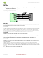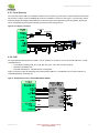
1
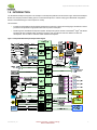
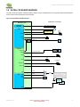
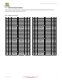
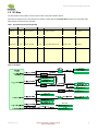
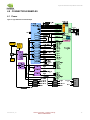
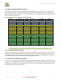
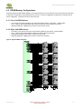
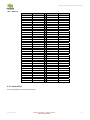
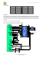
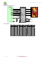
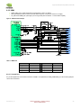
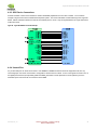
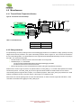
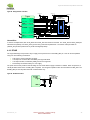
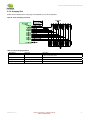
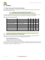
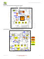
USER GUIDE Tegra™ 200 Series Developer Board Advance Information – Subject to Change NVIDIA CONFIDENTIAL January 2010 | DG-04927-001_v01 Document Change History 2 Version Date Description v01 JAN 22, 2010 Initial Release Advance Information – Subject to Change NVIDIA CONFIDENTIAL DG-04927-001_v01 Tegra 200 Series Developer Board User Guide Table of Contents 1.0 INTRODUCTION ....................................................................................................................................................................5 2.0 DEVELOPER BOARD OVERVIEW ........................................................................................................................................6 2.1 Feature List ........................................................................................................................................................................6 2.2 NVIDIA® Tegra™ 250 ........................................................................................................................................................8 2.3 System DRAM ....................................................................................................................................................................8 2.4 Boot Device ........................................................................................................................................................................8 2.5 LCD Interface .....................................................................................................................................................................9 2.6 External Display Support ....................................................................................................................................................9 2.7 Audio ..................................................................................................................................................................................9 2.8 USB ....................................................................................................................................................................................9 2.9 Storage .............................................................................................................................................................................10 2.10 Camera (optional) ...........................................................................................................................................................10 2.11 Wireless..........................................................................................................................................................................10 2.12 User Interface .................................................................................................................................................................11 2.13 Miscellaneous .................................................................................................................................................................11 2.14 Power .............................................................................................................................................................................11 3.0 SATELLITE BOARD HEADERS ...........................................................................................................................................12 3.1 Satellite Board Headers....................................................................................................................................................13 3.2 I2C Map ............................................................................................................................................................................14 4.0 CONNECTION EXAMPLES .................................................................................................................................................15 4.1 Power ...............................................................................................................................................................................15 4.1.1 Major Components ...................................................................................................................................................................... 16 4.1.2 Power Supplies............................................................................................................................................................................ 17 4.1.3 Power Sequencing ...................................................................................................................................................................... 18 4.1.4 Bypass Capacitor Recommendations ......................................................................................................................................... 19 4.1.5 Unused Interface Power Rails ..................................................................................................................................................... 19 4.1.6 Unused Power Management Signals .......................................................................................................................................... 19 4.2 Clocks...............................................................................................................................................................................20 4.2.1 32.768KHz Clock ......................................................................................................................................................................... 20 4.2.2 Oscillator Clock............................................................................................................................................................................ 20 4.3 DRAM Memory Configurations .........................................................................................................................................22 4.3.1 Four, 8-bit DDR2 devices ............................................................................................................................................................ 22 4.3.2 Eight, 8-bit DDR2 devices ........................................................................................................................................................... 22 4.3.3 Unused Pins ................................................................................................................................................................................ 23 4.4 NAND ...............................................................................................................................................................................24 4.5 USB ..................................................................................................................................................................................24 4.5.1 Force Recovery ........................................................................................................................................................................... 25 4.5.2 ULPI............................................................................................................................................................................................. 25 4.5.3 PCIe............................................................................................................................................................................................. 26 DG-04927-001_v01 Advance Information – Subject to Change NVIDIA CONFIDENTIAL 3 Tegra 200 Series Developer Board User Guide 4.6 Display..............................................................................................................................................................................27 4.6.1 LCD Displays ............................................................................................................................................................................... 27 4.6.2 HDMI ........................................................................................................................................................................................... 29 4.6.3 VGA (CRT) Out ........................................................................................................................................................................... 30 4.7 Camera.............................................................................................................................................................................31 4.7.1 Unused Pins ................................................................................................................................................................................ 31 4.8 SD/SDIO/MMC .................................................................................................................................................................32 4.8.1 SD/MMC Card Connections ........................................................................................................................................................ 32 4.8.2 eMMC Device Connections ......................................................................................................................................................... 33 4.8.3 SDIO Device Connections ........................................................................................................................................................... 34 4.8.4 Unused Pins ................................................................................................................................................................................ 34 4.9 Miscellaneous ...................................................................................................................................................................35 4.9.1 Thermal Diode (Temperature Sensor) ........................................................................................................................................ 35 4.9.2 Debug Interfaces ......................................................................................................................................................................... 35 4.9.3 EFUSE......................................................................................................................................................................................... 36 4.9.4 Strapping Pins ............................................................................................................................................................................. 37 5.0 THERMAL ............................................................................................................................................................................38 5.1 Major Component Thermal Specifications ........................................................................................................................38 5.2 Thermal Considerations for Components .........................................................................................................................38 DG-04927-001_v01 Advance Information – Subject to Change NVIDIA CONFIDENTIAL 4 Tegra 200 Series Developer Board User Guide 1.0 INTRODUCTION The Smartbook Development System is an example of a development platform built around the Tegra™ 200 Series Developer Board. This example provides a starting point for continued development; it outlines a fairly typical Smartbook configuration based on the NVIDIA® Tegra™ 250 Computer-on-a-Chip. This document: Provides recommendations and integration guidelines for engineers to follow when designing a Smartbook or similar product that is optimized for high performance and low power consumption. ® ™ Details a generic Smartbook Development System: development system consists of the NVIDIA Tegra 200 Series Developer Kit plus a satellite board containing most of the user input devices and some features for test and development; can be used for evaluation and/or software development. Figure 1. Example Smartbook Development System Block Diagram DG-04927-001_v01 Advance Information – Subject to Change NVIDIA CONFIDENTIAL 5 Tegra 200 Series Developer Board User Guide 2.0 DEVELOPER BOARD OVERVIEW 2.1 Feature List Applications Processor NVIDIA Tegra 250, 23x23mm ,0.8mm pitch SD/SDIO and HSMMC Standard SD/SDIO/MMC socket DRAM and Flash Memory 8, 128Mx8, DDR2 @ 333MHz TPS51116RGET DDR2 Buck Regulator Hynix 8-bit NAND on board Internal SD/MMC socket supports eMMC module USB and Ethernet SMSC LAN 9514 USB Hub and Ethernet 3 USB Type A Host ports USB for PCIE MiniCard Slot 2 Ethernet RJ-45 Jack SMSC USB3315 ULPI PHY USB for PCIE MiniCard Slot 1 USB Mini Type B connector for Recovery Mode Baseband USB based PCIe Mini Card Modules USIM Card Connector Buttons, Switches Power-On, Reset and Force-Recovery Buttons Display LVDS Bridge: TI SN75LVDS83B HDMI (Type A connector) Slim 15-pin VGA Connector Audio Miscellaneous Devices EC: SMSC MEC1308 Temperature Sensor: ADT7461AARMZ_RL7 Wolfson WM8903L Codec Stereo Headphones External and Internal Mics Left/Right Speaker Amps. Imaging Dual-lane MIPI CSI connection for camera module Wireless Murata WiFi and Bluetooth module Bluetooth: CSR BC6 802.11b/g WiFi: Atheros 6002 - Power PMIC: TI TPS658621AZGUR Battery Charge Controller: TI BQ24745RHDR Main system regulators 3.3V, 5V, 1.8V and 1.05V Other, lower power regulators 3.3V (standby), 1.2V and 1.5V Debug / Test Features 22-pin Debug Connector JTAG, UART and SPI Tegra Debug Module (optional) This is an optional module that may have been shipped with your Tegra 200 Series Developer Board depending on the version of the development kit that was ordered. DG-04927-001_v01 Power, Reset and Force-Recovery Buttons Lid Open/Close slider switch UART4 (4-pin UART) brought to RS232 DB9 serial connector (intended for software test and debug) Adds a coin cell battery for uninterrupted Real-Time Clock operation when the developer board is powered off Advance Information – Subject to Change NVIDIA CONFIDENTIAL 6 Tegra 200 Series Developer Board User Guide Figure 2. Tegra 200 Series Developer Board (Top View) VGA Conn (J12) LCD (J7) AC/DC Jack (J15) Camera (J9) HDMI Conn (J18) PCIE MiniCard 0 (J27) WiFi Ant (J24) Mini-B USB SIM Card (J19) SD/MMC (J5) Battery Con (J14) Tegra T20 (U4) Ethernet Jack (J4) PMU (U7) DDR2 (Rank 0) USB Host Port (J25) Dual USB Host Ports (J6) Headphn Jack (J1) MMC VCORE (J20) Debug Conn (J10) PCIE MiniCard 1 (J27) Internal SD/MMC (J26) Mic Jack (J2) Int Mic (J8) On Left Spkr Button (J11) (S1) Force Rec Reset Button Button (S2) (S3) Satellite Headers (J16, J17) Right Spkr (J21) Figure 3. Tegra 200 Series Developer Board (Bottom View) DG-04927-001_v01 Advance Information – Subject to Change NVIDIA CONFIDENTIAL 7 Tegra 200 Series Developer Board User Guide 2.2 NVIDIA® Tegra™ 250 The NVIDIA Tegra 250 computer-on-a-chip is suited for handheld and mobile applications. It’s primary purpose is to control all system peripherals and provide computing power. Table 1 Features (Available / Used on Tegra 200 Series Developer Board) CPU Dual-core ARM® Cortex-A9 MPCore™ processor External Memory Support 32-bit 333MHz DDR2 SDRAM (to 1GB) 2 chip selects Dynamic voltage and frequency scaling Multiple clock and power domains Independent gating of power domains Integrated Open GLES 2.0 3D core SPI (Qty 1), I2C (Qty 3), UART (Qty 2) I2S/PCM (Qty 2) ULPI HS USB 2.0 HS (Qty 3) SDIO (Qty 3) Internal 4-bit SD/8-bit MMC o eMMC compatible module available External 4-bit MMC/SD Dual Display (Integrated LCD + external) 18-bit LVDS LCD HDMI to 1080p and VGA Camera (CSI) Pre/Post Processing Acceleration with ISP MPEG-4/H264/JPEG Encoder Advanced Power Management 2D/3D acceleration Connectivity and Expansion Storage Multimedia Support Note: For more information on Tegra 250, refer to the Tegra 200 Series Datasheet (Electrical, Mechanical and Thermal Specifications and the Design Guide. 2.3 System DRAM The Tegra 200 Series Developer Board has 8 DDR2 128M x 8 devices for 1GB total system DRAM. The DDR2 will operate up to 333MHz for a peak bandwidth of 2.7GB/s. The memory is arranged as one or two 32-bit Ranks. Each Rank uses a different Chip Select and Clock Enable. For low power operation with memory retention, self refresh is supported. 2.4 Boot Device A 4Gb (512MB) Hynix HY27UF084G2BTPCB 8-bit NAND is available for use as the boot device. In addition, an internal 4-bit SD, 8-bit MMC socket (J26) is provided to support other flash memories. DG-04927-001_v01 Advance Information – Subject to Change NVIDIA CONFIDENTIAL 8 Tegra 200 Series Developer Board User Guide 2.5 LCD Interface The Smartbook Development System routes an 18-bit parallel RGB interface from the Tegra 250 to a Texas Instruments SN75LVDS83B LVDS Transmitter which goes to an LVDS panel connector (J7). The connector is a Foxconn GS13307-112307F. The controls available for the panel and backlight include: Panel power provided by main 3.3V Buck regulator and enabled by the Tegra 250 GPIO on LCD_PWR2 (EN_VDD_PNL) Backlight enable controlled by the Tegra 250 GPIO on pin SDIO3_DAT2 (SDIO block) Backlight PWM controlled by PM3_PWM0 on SDIO3_DAT3 (SDIO block) Backlight power provided from VDD_VBAT (battery or AC/DC adapter) and enabled by the Tegra 250 GPIO on LCD_CS1_N LVDS Transmitter shutdown enabled by Tegra 250 GPIO on pin LCD_PWR0 2.6 External Display Support A standard HDMI Type A connector (J18) is provided and supports up to 1080p60Hz operation. The Tegra 200 Series Developer Board supports Hot Plug Detect by routing the HP_DET line on the HDMI connector to the Tegra 250 HDMI_INT_N interrupt pin. The DDC interface is shared between HDMI and the VGA interface, so only one of these displays can be connected at a time. A standard 15-pin VGA connector (J12) is also provided and supports resolutions up to 1600x1200. The Tegra 200 Series Developer Board also supports detection of a VGA device connection. This uses the Tegra 250 pin SPI2_SCK on the Audio block. 2.7 Audio The Tegra 200 Series Developer Board integrates the Wolfson Microelectronics WM8903 Ultra Low Power CODEC for Portable Audio Applications. The Tegra 250 DAP1 interface supporting I2S protocol communicates audio data to/from the CODEC. GEN1_I2C is used for CODEC configuration. The audio subsystem features: Left and Right amplified speaker output via two Wolfson WM9001 amplifiers Headers for connecting Left (J11)/Right (J21) speakers Stereo headphone jack (J1) Both internal Microphone (J8) and external microphone jack (J2) 2.8 USB The Tegra 250 has three available USB controllers. Controllers #1 and #3 come out on the USB PHYs on the USB1 and USB3 pins. Controller #2 can be used for either ULPI or HSIC (only one at a time). All three USB controllers are used on the Tegra 200 Series Developer Board. Controller #1 USB1 (PHY) is required for Recovery mode and so is brought out to a USB Mini B connector (J3). USB1 is configured as a device to allow connection to a host PC, typically for flashing images at the factory or possibly in the field. Controller #2 USB2 provides a ULPI interface on the Tegra 200 Series Developer Board and connects to an external USB3315 ULPI PHY. The PHY then connects to PCIe Mini-Card 0 (J27) which is intended for a 3G baseband module. Controller #3 USB3 (PHY) is routed to an SMSC LAN9514 USB Hub and Ethernet controller. This controller provides one Ethernet interface and four USB Host ports. The Tegra 200 Series Developer Board routes the Ethernet signals to a standard RJ-45 jack. Three DG-04927-001_v01 Advance Information – Subject to Change NVIDIA CONFIDENTIAL 9 Tegra 200 Series Developer Board User Guide of the USB ports are brought to standard Type A connectors (J6 – Dual host port connector and J25 – Single host port). The forth USB is routed to PCIe Mini-Card #1 (J28). 2.9 Storage There are two SD/MMC sockets on the Tegra 200 Series Developer Board. Both sockets support High Speed operation (52MHz for MMC, 50MHz for SD/SDIO) SD/MMC Socket 1 (J26) The J26 SD/MMC socket is a combination 8-bit MMC and 4-bit SD/MMC socket intended to be for internal storage, most likely an eMMC module. Although this device is in a socket, it is not meant to be used as removable storage in a real design. 3.3V is supplied to the socket. There is also a 2-pin header (J5) to supply a core rail at 2.85V. This header is used when the eMMC module is installed in this socket. SD/MMC Socket 2 (J5) The J5 SD/MMC Socket is a removable storage is a standard 4-bit SD/MMC socket. This would normally be located to allow SD/MMC/SDIO cards to be inserted and removed by the user. 3.3V is supplied to this socket. 2.10 Camera (optional) A socket for a camera module is provided on the Tegra 200 Series Developer Board (J9). 2.11 Wireless Bluetooth and Wifi The Tegra 200 Series Developer Board integrates a MuRata BT/WF Module using the CSR-BC6 and Atheros AR6002 controllers. The Bluetooth 2.0 transceiver sends and receives on a 2.4GHz line, including Enhanced Data Rates (EDR) up to 3Mbps and scatter-net support. USB and Dual UART Ports with rates up to 3MBaud are supported. It operates at full speed Bluetooth operation with full piconet support and co-exists with 802.11. The CSR device will act as a serial peripheral when connected to the Tegra 250 via a serial port. This interface, as with WiFi below, will be implemented on a substrate (typically LTCC) supplied by MuRata containing all components required for operation, to minimize tuning and testing. An external antenna for 2.4GHz (available off the shelf) is also required The 802.11b/g transceiver sends and receives on a 2.4GHz line at 54Mbps max. It provides full QoS for 802.11e and security support 802.11i and co-exists with the Bluetooth device. The interface of choice is SDIO. This interface will be implemented on a LTCC substrate supplied by MuRata and soldered down to our board to minimize tuning and testing. An external antenna supporting both Bluetooth and WiFi for 2.4GHz (available off the shelf) is required and available from a variety of suppliers. PCIe Mini-Card (3G Modem support and more) The Tegra 200 Series Developer Board provides two PCIe Mini-Card slots. Both slots support PCIe operation as well as USB 2.0 High Speed. Slot #0 (J27) also routes to a UIM SIM socket (J19) and is intended to support compatible 3G Modem modules. PCIe Mini-Card slot #1 (J28) could be used for other peripherals such as Solid-State drives or a different WiFi solution. Note: DG-04927-001_v01 Contact NVIDIA for list of certified PCI express peripherals Advance Information – Subject to Change NVIDIA CONFIDENTIAL 10 Tegra 200 Series Developer Board User Guide 2.12 User Interface Attach your USB keyboard and mouse to any of the available USB Type-A Host ports (J6, J25). 2.13 Miscellaneous Temperature Sensor On Semiconductor Model ADT7461AARMZ_RL7 0.25°C resolution/1°C accuracy (remote channel used) Interfaces to PWR_I2C Programmable over/under temperature limits Debug Options The Tegra 200 Series Developer Board provides development/debugging interfaces including JTAG, UART and Ethernet. The Tegra Debug Module [E1173] interfaces to the Tegra 200 Series Developer Board using the expansion headers. This board provides: A UART interface through a RS232 DB9 serial connector (intended for software test and debug) Remote POWER, RESET and FORCE RECOVERY buttons Adds a coin cell battery for uninterrupted Real-Time Clock operation when the developer board is powered off 2.14 Power Power Source Battery: 3-Cell, Li Ion, 24WHr, 11.1V Nominal AC/DC Adapter: TopMagnetics HK-HW30-A15, 15/30W 100V – 240V operation Battery Charge Controller Texas Instruments BQ24745RHDR PMU Texas Instruments TPS658621AZGUR Dedicated DC/DCs Main system 3.3V and 5V rails: Texas Instruments TPS51220ARTVT Main system 1.8V: Texas Instruments TPS51116RGER PCIe 1.05V for the Tegra 250: Texas Instruments TPS62290DRVR External LDOs 1.2V: Texas Instruments TPS72012YZUT 1.5V: Texas Instruments TPS74201RGWR DG-04927-001_v01 Advance Information – Subject to Change NVIDIA CONFIDENTIAL 11 Tegra 200 Series Developer Board User Guide 3.0 SATELLITE BOARD HEADERS Two dual row 50-pin expansion headers enable the ability to connect a satellite board to the Tegra 200 Series Developer Board and are used to extend developer board functionality. Figure 4. Example Satellite Board Block Diagram Tegra 200 Series Developer Board (E1162) Wireless Modules Additional Functionality LEDs (WPAN, WWAN, WLAN) Coin Cell PMU RESET Button LEDs (PWR, CHG, NUM, CAPS, SCROLL, RF) ONKEY ONKEY Button RESET I2C ID EEPROM PWR_I2C PROG HDR Tegra 2 PWR_I2C UART4 RS-232 TRCV Tx, Rx, RTS, CTS DB9 CON LID_Status Switch GPIO RF On/Off Switch GPIO ForceRecovery Button GMI_RE_N CAM_I2C KBC EC KBC 16x8 18x8 Res Mux 16x8 C GPIO GPIO HeartBeat LED I2C Touchpad or PS/2 Touchpad PS/2 DG-04927-001_v01 Advance Information – Subject to Change NVIDIA CONFIDENTIAL 12 Tegra 200 Series Developer Board User Guide 3.1 Satellite Board Headers All the interface connections between a satellite board and the Tegra 200 Series Developer Board are through two sets of Samtec FTS series 50-pin Micro Strips connectors. Table 2. Satellite Connectors Pinout Dir Pin # Signal Name Signal Name Pin # Dir Dir Pin # Signal Name Signal Name Pin # Dir In 1 KB_COL7 EC_KSO17 2 Out Out 1 LED_WPAN* VDD_CELL_RMT 2 In In 3 KB_COL6 EC_KSO16 4 Out Out 3 LED_WLAN* UART4_TXD 4 Out In 5 KB_COL5 EC_KSO15 6 Out Out 5 LED_WWAN* VDDIO_NAND_MB 6 Out In 7 KB_COL4 EC_KSO14 8 Out In 7 W_DISABLE * UART4_RXD 8 In In 9 KB_COL3 EC_KSO13 10 Out Out 9 LED_WIFI_BT * UART4_CTS* 10 In In 11 KB_COL2 EC_KSO12 12 Out Out 11 LED_CHARGE* UART4_RTS* 12 Out In 13 KB_COL1 EC_KSO11 14 Out Out 13 LED_POWER* NO CONNECT 14 In 15 KB_COL0 EC_KSO10 16 Out Out 15 LED_SCROLL_LOCK* FORCE_ACOK 16 In Out 17 KB_ROW15 EC_KSO9 18 Out Out 17 LED_CAPS_LOCK* VDDIO_SYS_MB 18 Out Out 19 KB_ROW14 EC_KSO8 20 Out Out 19 LED_NUM_LOCK* PWR_I2C_SCL 20 Bi Out 21 KB_ROW13 EC_KSO7 22 Out 21 GND PWR_I2C_SDA 22 Bi Out 23 KB_ROW12 EC_KSO6 24 Out In 23 SPDIF_IN VDD_3V3_MB 24 Out Out 25 KB_ROW11 EC_KSO5 26 Out Out 25 SPDIF_OUT VDD_3V3_MB 26 Out Out 27 KB_ROW10 EC_KSO4 28 Out Out 29 KB_ROW9 EC_KSO3 30 Out Out 31 KB_ROW8 EC_KSO2 32 Out In Out 33 KB_ROW7 EC_KSO1 34 Out In Out 35 KB_ROW6 EC_KSO0 36 Out Out Out 37 KB_ROW5 EC_KSI7 38 In Out Out 39 KB_ROW4 EC_KSI6 40 In In 39 Out 41 KB_ROW3 EC_KSI5 42 In In Out 43 KB_ROW2 EC_KSI4 44 In Out 45 KB_ROW1 EC_KSI3 46 In In Out 47 KB_ROW0 EC_KSI2 48 In In In 49 EC_KSI0 EC_KSI1 50 In In DG-04927-001_v01 Out 27 GND GND 28 29 IR_TXD PS2_TS_CLOCK 30 Bi 31 IR_RXD PS2_TS_DATA 32 Bi 33 LID_OPEN* GND 34 35 VDD_5V0_MB CAM_I2C_SDA 36 Bi 37 VDD_5V0_MB CAM_I2C_SCL 38 Bi TP_IRQ* GND 40 41 TS_IRQ* PS2_TP_CLOCK 42 Bi 43 NO CONNECT PS2_TP_DATA 44 Bi 45 ONKEY* LED_HEARTBEAT* 46 Out 47 FORCE_RECOVERY* SYS_RESET_B* 48 Out 49 RESET* VDD_3V3_EC_MB 50 Out Advance Information – Subject to Change NVIDIA CONFIDENTIAL 13 Tegra 200 Series Developer Board User Guide 3.2 I2C Map The I2C interface can be used to connect a touch screen, touch pad and other devices. There are two options for the Touch devices. I2C versions of these devices (recommended) interface to the Tegra 250, while PS/2 versions connect to the EC controller. Table 3. Tegra 200 Series Developer Board I2C Map Domain Contrlr Pins Volt. Device ID / I2C Addr Location Main Board VDDIO_VI I2C3 CAM_I2C_SCL/SDA 3.3V MEC1308 (I2C Master) Tegra 250 Slave addr: 0x45 VDDIO_VI I2C3 CAM_I2C_SCL/SDA 3.3V Touchpad 0x28 Remote Location VDDIO_VI I2C3 CAM_I2C_SCL/SDA 3.3V Touchscreen TBD Remote Location VDDIO_UART I2C1 GEN1_I2C_SCL/SDA 1.8V Camera 0x36 Main Board VDDIO_UART I2C1 GEN1_I2C_SCL/SDA 1.8V Autofocus DAC 0x0C Main Board VDDIO_UART I2C1 GEN1_I2C_SCL/SDA 3.3V Option for SMB to Battery Pack Pack is Master or Slave Slave addr: 0x0B Main Board VDDIO_UART I2C1 GEN1_I2C_SCL/SDA 3.3V Option for SMB to Charger 0x09 Main Board I2C2 DDC_SCL/SDA 5.0V Mini VGA or HDMI Display 0x30, 0x50, 0x52 Main Board 1.8V TI TPS658621 PMU 0x34 Main Board VDDIO_LCD VDDIO_SYS VDDIO_UART PWR_I2C PWR_I2C_SCL/SDA I2C1 1.8V WM8903 Audio Codec 0x1A Main Board VDDIO_SYS PWR_I2C 1.8V ID EEPROM 0x50 Main Board VDDIO_SYS PWR_I2C 1.8V ID EEPROM 0x51 Remote Location VDDIO_SYS PWR_I2C 1.8V Temperature Sensor 0x4C Main Board Figure 5. I2C Diagram DG-04927-001_v01 Advance Information – Subject to Change NVIDIA CONFIDENTIAL 14 Tegra 200 Series Developer Board User Guide 4.0 CONNECTION EXAMPLES 4.1 Power Figure 6. Tegra 250 Power Connection Example DG-04927-001_v01 Advance Information – Subject to Change NVIDIA CONFIDENTIAL 15 Tegra 200 Series Developer Board User Guide 4.1.1 Major Components 4.1.1.1 PMU The Tegra 200 Series Developer Board includes a multi-channel power management unit for embedded processors (TI TPS658621). Feature List Host Interface I2C Control I/F Core/CPU power request signals 32.768KHz Clock Reset input Reset output RTC LDO 1.0V-1.2V nominal voltage range with 25mV steps Separate LDO for RTC domain allowing Deep Sleep mode support – the Tegra 250 lowest power mode Switch RTC domain automatically back to 1.2V when wake-up event detected (w/CORE_PWR_REQ) CORE switcher 1.0V-1.2V nominal voltage range with 25mV steps CORE and RTC domains must track each other within 170mV Tracking can be ensured in software Optimized DVS handled by NVIDIA BSP (DVFS architecture) Turned off if CORE_PWR_REQ is de-asserted – on at 1.2V when CORE_PWR_REQ asserted CPU switcher 0.85-1.0V nominal voltage range with 25mV steps Optimized DVS handled by NVIDIA BSP (DVFS architecture) Turned off if CPU_PWR_REQ is de-asserted – on at 1.0V when CPU_PWR_REQ asserted PLL LDO Use 1.1V LDO Very good line regulation ensured using DC/DC switcher as LDO source STDBY input Standby mode: Only the minimum rails are kept powered (RTC and SYSTEM domains, DDR2 in self-refresh) The Tegra 250 indicates Standby mode by de-asserting CORE_PWR_REQ (polarity programmable) 4.1.1.2 Battery Charge Controller The Tegra 200 Series Developer Board includes a battery charger with input current detect comparator and charge enable pin (TI bq24745). For a detailed description and list of device features, see http://focus.ti.com/lit/ds/symlink/bq24745.pdf. 4.1.1.3 Battery Pack (Not Included) The Tegra 200 Series Developer Board can be used with a 3 cell (3S1P) Lithium ion battery pack that has a nominal voltage of 10.8 volts and a total capacity of 2200mAh. The 3S1P is ideal for applications that can operate on lower voltages. 4.1.1.4 External Switchers, LDOs, Power Switches The Tegra 200 Series Developer Board includes the following components: Notebook System Power Controller (TI TPS51220): a dual synchronous buck regulator controller with 2 LDOs. For a detailed description and list of device features, see http://focus.ti.com/lit/ds/symlink/tps51220.pdf. DDR2 Memory Power Supply (TI TPS51116): provides a power supply for the DDR2memory system. For a detailed description and list of device features, see http://focus.ti.com/lit/ds/symlink/tps51116.pdf. 350mA Low-Dropout Linear Regulator (TI TPS72012): for a detailed description and list of device features, see http://focus.ti.com/lit/ds/symlink/tps72012.pdf. Step Down Converter (TI TPS62290): synchronous step down dc-dc converter optimized for battery powered portable devices. For a detailed description and list of device features, see http://focus.ti.com/lit/ds/symlink/tps62290.pdf. 135-mΩ Dual Power-Distribution Switch (TI TPS2052): for a detailed description and list of device features, see http://focus.ti.com/lit/ds/symlink/tps2052.pdf. 135-mΩ Power Distribution Switch (TI TPS2051): for a detailed description and list of device features, see http://focus.ti.com/lit/ds/symlink/tps2051.pdf. DG-04927-001_v01 Advance Information – Subject to Change NVIDIA CONFIDENTIAL 16 Tegra 200 Series Developer Board User Guide 4.1.2 Power Supplies The Tegra 250 has 29 power rails (3 cores, 14 analog and 12 digital I/O). Depending on system design, many of the rails can share a power supply, and some are not needed for all designs. The example shown in Table 4 is based on the Smartbook Development System design and should be representative of these types of designs. This table mainly lists the supplies required by the Tegra 250. Others are required to support some of the peripherals typically seen in a Smartbook. Table 4 Tegra 250 Power Supply Allocation Example Power Rails Supported Voltages (V) Voltage (V) (Tegra 200 Series DB) Power Supply Enable VDD_RTC 1.0 – 1.2 Up to 1.2 PMU LDO2 PMU SM2 (3.7V) + Internal Trigger VDD_CORE 1.0 – 1.2 Up to 1.2 PMU SM0 CORE_PWR_REQ + Internal Trigger VDD_CPU 0.9 – 1.0 Up to 1.0 PMU SM0 CPU_PWR_REQ + Internal Trigger AVDD_PLLx 1.1 1.1 PMU LDO1 PMU SM2 (3.7V) + Internal Trigger VDDIO_SYS, AVDD_OSC 1.8 1.8 PMU LD04 PMU SM2 (3.7V) + Internal Trigger VDDIO_LCD,VDDIO_BB,VDDIO_AUDIO,VDDIO_UART VDDIO_DDR 1.8,2.8,3.3 1.8 1.8 TPS51116, DC/DC EN_VDD_1V8 (PG_VDDIO_SYS – PMU LDO4PG) AVDD_USB, AVDD_USB_PLL 3.3 3.3 PMU LDO3 PMU SM2 (3.7V) + Internal Trigger VDD_DDR_RX 2.8 2.8 PMU LDO9 PMU SM2 (3.7V) + Internal Trigger VDDIO_NAND (if 3.3V), VDDIO_SDIO, VDDIO_VI 1.8,2.8,3.3 3.3 TPS51220, DC/DC EN_VDD_3V3 (Output of SR) AVDD_VDAC 2.7 – 3.3 2.85 PMU LDO6 PMU SM2 (3.7V) AVDD_HDMI 3.3 3.3 PMU LDO7 PMU SM2 (3.7V) AVDD_HDMI_PLL 1.8, 2.5 1.8 PMU LDO8 PMU SM2 (3.7V) VDDIO_PEX_CLK 3.3 3.3 PMU LDO0 PMU SM2 (3.7V) AVDD_DSI_CSI 1.2 1.2 TPS72012, LDO2 EN_VDD_1V2 (PMU GPIO) AVDD_PCIE, AVDD_PEX, AVDD_PEX_PLL, VDD_PEX 1.05 1.05 TPS62290, DC/DC EN_VDD_1V05 (PMU GPIO) VCORE_MMC 2.7 – 3.6 2.85 PMU LD05 Note: DG-04927-001_v01 1: This includes pins AVDD_PLLA_C_P (powers PLLA, PLLC and PLLP), AVDD_PLLM, AVDD_PLLU (powers PLLU and PLLD) and AVDD_PLLX. If PCIE not supported in a design, AVDD_PCIE should be left unpowered as the leakage is significant. 2: Supplies must meet maximum rate requirement in AP20 EMT of 165mV/us Advance Information – Subject to Change NVIDIA CONFIDENTIAL 17 Tegra 200 Series Developer Board User Guide 4.1.3 Power Sequencing The Power solution, including the PMU and any external supplies/logic, must be able to meet the Tegra 250 power sequence requirements. These requirements are detailed in the Tegra 200 Series datasheet (Electrical, Mechanical and Thermal Specifications). Figure 7 shows the sequence used for the Smartbook Development System. Figure 7. Power-up Sequence Example VBAT (10.2-12.6V, 15V) VDD_5V0 (5V, DC/DC TPS51220A) VDD_3V3_SBY (3.3V, DC/DC TPS51220A) BATTERY or AC/DC VDDIO_ONKEY (2.2V, PMU LDO) PMU SUPPLY ONKEY (VDD_2V2) VDD_SM2 (3.7V, PMU SM2) EXTERNAL SUPPLY VDD_RTC (1.2V, PMU LDO2) Signals VDD_CORE (1.2V, PMU SM0) AVDD_PLL (1.1V, PMU LDO1) VDDIO_SYS/AVDD_OSC (1.8V, PMU LDO4) CLK_32K_IN (PMU) 32KHz Ramp Time System Clock (External Source or XTAL) Oscillator Ramp Time VDD_1V8 (1.8V, DC/DC TPS51116) V2REF_DDR2 (0.9V, DC/DC TPS51116) AVDD_USB / USB_PLL (3.3V, PMU LDO3) VCORE_MMC (2.85V, PMU LDO5) VDD_DDR_RX (2.85V, PMU LDO9) VDD_3V3 (3.3V, DC/DC TPS51220A) VDD_CPU (1.0V, PMU SM1) SYS_RESET_N (PMU) AVDD_VDAC (2.85V, PMU LDO6) AVDD_HDMI (3.3V, PMU LDO7) Off by Default AVDD_HDM_PLL (1.8V, PMU LDO8) VDDIO_PEX_CLK (3.3V, PMU LDO0) Misc. 1.5V, 3.3V, 5.0V, Backlight GPIO Enabled AVDD_DSI_CSI (1.2V, LDO TPS72012) VDD_1V05 (1.05V, DC/DC TPS62290) VDD_3V3: VDDIO_NAND_3V3, VDDIO_SDIO,VDDIO_VI VDD_1V8: VDDIO_NAND_1V8, VDDIO_LCD, VDDIO_BB, VDDIO_AUDIO, VDDIO_UART, VDDIO_DDR VDD_1V05: AVDD_PLLE, AVDD_PEX, AVDD_PEX_PLL, VDD_PEX Note: DG-04927-001_v01 1: VDD_RTC, VDD_CORE, Critical PLLs, AVDD_OSC, VDDIO_SYS, VDDIO_DDR, VDDIO_NAND, 32.768KHz and System clocks required before SYS_RESET_N goes high 2: Recommended Power-down sequence is reverse of Power-up. Advance Information – Subject to Change NVIDIA CONFIDENTIAL 18 Tegra 200 Series Developer Board User Guide 4.1.4 Bypass Capacitor Recommendations Table 5 lists the basic recommendations for bypass capacitors near the Tegra 250. In general, one 0.1uf per power pin (or group for cores) is desirable. These should be placed as close as possible to the respective power pins. In addition, for the higher power/higher frequency I/O rails one or more 4.7uf bulk capacitor is recommended and should be placed in the general area of the power and interface pins. Table 5 Power Supply Capacitor Recommendations for Tegra 250 Supplies Power Rail 0.1uF Bypass Capacitors 4.7uF Bulk Capacitors VDD_CORE 3 2 VDD_RTC 1 Power Rail 0.1uF Bypass Capacitors 4.7uF Bulk Capacitors VDD_CPU 1 3 AVDD_HDMI 1 AVDD_USB_PLL 1 Cores Analog AVDD_PLLn1 1 each AVDD_DSI_CSI 1 AVDD_OSC 1 AVDD_VDAC 1 AVDD_HDMI_PLL 1 AVDD_PEX_PLL AVDD_USB 1 AVDD_IC_USB 1 AVDD_PEX 1 1 AVDD_PLLE 1 6 VDDIO_DDR_RX 1 Digital VDDIO_DDR 1 VDDIO_NAND 1 1 VDDIO_VI 1 1 VDDIO_HSIC 1 1 VDDIO_SDIO 1 1 VDDIO_BB 1 1 VDDIO_SYS 1 VDDIO_LCD 1 VDDIO_UART 1 VDDIO_AUDIO 1 VDDIO_PEX_CLK 1 VDD_PEX 0 Note: 1 1: AVDD_PLLA_P_C, AVDD_PLLM, AVDD_PLLU, AVDD_PLLX 4.1.5 Unused Interface Power Rails The example also assumes that all the interfaces are to be used. If a design does not use any functions on one or more of the interface blocks, the associated power rail does not need to be powered. For the correct handling of each of the rails in this case, check the Unused Pin section under for the interface in this document. Generally, unused digital power rails can be left unconnected or tied to ground while unused analog rails should be left unconnected. 4.1.6 Unused Power Management Signals A few of the signals related to power management may not be required in some designs. This includes SYS_CLK_REQ and CLK_32K_OUT. If not required, these pins can be configured as GPIOs instead. CORE_PWR_REQ may also not be needed in all designs, but this pin does not have a GPIO option. If any of these pins are not used, either as their primary function or as a GPIO (if available), they can be left unconnected. DG-04927-001_v01 Advance Information – Subject to Change NVIDIA CONFIDENTIAL 19 Tegra 200 Series Developer Board User Guide 4.2 Clocks The Tegra 250 has a large number of internal functional blocks supporting a broad range of interfaces. Each of these has its own clocking requirements. The RTC (Real Time Clock) and PMC (Power Management Controller) require a 32.768KHz clock, to be provided externally. In addition, a higher frequency reference clock (OSC) is required. This can come from a crystal or an external source, and feeds several integrated PLLs that provide a variety of clocking options for the core and I/O blocks. The Tegra 250 clocking scheme is shown in Figure 8. Figure 8. Tegra 250 Clocking Block Diagram 4.2.1 32.768KHz Clock The 32.768KHz clock is provided externally by the PMU. This clock is input on the CLK_32K_IN pin which is referenced to the VDDIO_SYS rail. See the Tegra 200 Series Datasheet (Electrical, Mechanical and Thermal Specifications) for details on the requirements for this clock. 4.2.2 Oscillator Clock The Tegra 200 Series Developer Board utilizes a 12MHz crystal connected to the Tegra 250 XTAL_IN, XTAL_OUT pins to generate the reference clock internally. A reference circuit is shown in Figure 9. Table 6 contains the requirements for the crystal used, the value of the parallel bias resistor and information to calculate the values of the two external load capacitors (CL1 and CL2) shown in the circuit. DG-04927-001_v01 Advance Information – Subject to Change NVIDIA CONFIDENTIAL 20 Tegra 200 Series Developer Board User Guide Figure 9. Crystal Connection Example Table 6 Crystal and Circuit Requirements Note: DG-04927-001_v01 Symbol Parameter FP Parallel resonance crystal Frequency Min FTOL Frequency Tolerance CL Load Capacitance for crystal parallel resonance DL Crystal Drive Level RBIAS External Bias Resistor ESR Equivalent Series Resistance 5 Typ Max Unit 12 MHz ±50 ppm 7 10 pf 300 uW 2 MΩ 80 Ω FP, FTOL, CL and DL are found in the Xtal Datasheet ESR = RM * (1 + C0/CL)/2 where RM = Motional Resistance, C0 =Shunt Capacitance from Xtal datasheet. Datasheets may specify ESR directly – consult manufacturer if unclear whether ESR or RM are specified. Load capacitor values (CLx) can be found with formula CL = [(CL1xCL2)/(CL1+CL2)]+CPCB Or since CL1 and CL2 are typically of equal value, CL = (CLx/2)+CPCB. or CLx = (CL – CPCB) x 2 CL = Load capacitance (Xtal datasheet). CPCB is PCB capacitance (trace, via, pad, etc.) Advance Information – Subject to Change NVIDIA CONFIDENTIAL 21 Tegra 200 Series Developer Board User Guide 4.3 DRAM Memory Configurations Tegra 250 supports standard DDR2 SDRAM. Up to 1GB total memory, two chip selects and two Clock Enables are supported. A full 8-device configurations using x8 DDR2 devices is shown. A 4 device configuration is possible and is a subset of the 8 device configuration. Only Rank 0 would be used in this case. 4.3.1 Four, 8-bit DDR2 devices Four Devices are routed in parallel to form single 32-bit memory Rank (1 Chip Select, 1 Clock Enable) CLK+/-, Address, BA, RAS/CAS/WR, CKE0, CS0 and ODT0 are routed to all devices (4 loads) DQ[31:0], DQS[3:0]+/-, DQM[3:0] are routed to one device each (1 load) 4.3.2 Eight, 8-bit DDR2 devices Two Ranks of four devices each form two 32-bit memory Ranks (2 Chip Selects, 2 Clock Enables) CLK+/-, Address, BA, RAS/CAS/WR and ODT0 are routed to all devices (8 loads) CKE[1:0] and CS0[1:0]_N are routed to 4 devices each (4 loads) DQ[31:0], DQS[3:0]+/-, DQM[3:0] are routed to 2 devices each (2 loads) Figure 10. Eight, 8-bit DDR2 Configuration DG-04927-001_v01 Advance Information – Subject to Change NVIDIA CONFIDENTIAL 22 Tegra 200 Series Developer Board User Guide Table 7. DDR Pinout Signal Pin Signal Pin DDR_A0 A20 DDR_DM0 F19 DDR_A1 C24 DDR_DM1 E15 DDR_A2 D20 DDR_DM2 G23 DDR_A3 B20 DDR_DM3 D9 DDR_A4 F26 DDR_DQ0 F20 DDR_A5 C26 DDR_DQ1 E18 DDR_A6 C27 DDR_DQ2 D18 DDR_A7 F28 DDR_DQ3 F18 DDR_A8 A26 DDR_DQ4 F17 DDR_A9 A23 DDR_DQ5 E21 DDR_A10 D23 DDR_DQ6 D21 DDR_A11 C20 DDR_DQ7 F21 DDR_A12 C18 DDR_DQ8 E17 DDR_A13 E28 DDR_DQ9 D15 DDR_A14 C28 DDR_DQ10 F16 DDR_CLK E26 DDR_DQ11 E14 DDR_CLK_N E27 DDR_DQ12 F13 DDR_CAS_N H26 DDR_DQ13 D16 DDR_CKE0 A21 DDR_DQ14 D12 DDR_CKE1 C21 DDR_DQ15 D13 DDR_CS0_N E25 DDR_DQ16 F23 DDR_CS1_N C23 DDR_DQ17 F25 DDR_BA0 B26 DDR_DQ18 H22 DDR_BA1 A24 DDR_DQ19 G25 DDR_BA2 B24 DDR_DQ20 F22 DDR_QUSE0 G15 DDR_DQ21 D24 DDR_QUSE1 G17 DDR_DQ22 H24 DDR_QUSE2 A18 DDR_DQ23 E23 DDR_QUSE3 B18 DDR_DQ24 F9 DDR_RAS_N B23 DDR_DQ25 F12 DDR_WE_N F27 DDR_DQ26 E12 DDR_DQS0P E20 DDR_DQ27 E9 DDR_DQS0N D19 DDR_DQ28 F10 DDR_DQS1p F15 DDR_DQ29 G8 DDR_DQS1N F14 DDR_DQ30 F11 DDR_DQS2p F24 DDR_DQ31 G9 DDR_DQS2N E24 DDR_DQS3p D10 DDR_DQS3N E11 4.3.3 Unused Pins Any unused signal pins can be left unconnected. DG-04927-001_v01 Advance Information – Subject to Change NVIDIA CONFIDENTIAL 23 Tegra 200 Series Developer Board User Guide 4.4 NAND The Tegra 250 GMI interface supports a broad range of devices including a variety of NAND devices and configurations. Works with SLC and MLC devices Supports up to 8 devices with up to 8 chip selects Figure 11. Single 8-bit NAND Connection Example 4.5 USB The Tegra 250 has three available USB controllers. Controllers #1 and #3 come out on the USB PHYs on the USB1 and USB3 pins. Controller #2 can be used for either ULPI or HSIC (only one at a time). Controller #1 This USB controller is routed to an integrated PHY (USB1) and supports low-, full- and high-speed mode. Both Host and Device modes are supported. VBUS and Device ID are available to support Type A, B or A/B connector types. USB1 is required for Recovery mode and must be configurable as a USB Device when the Force Recovery strap (on pin GMI_OE_N is held low. In this case, USB1 is connected to a host, typically for flashing images at the factory or possibly in the field. Controller #2 Controller #2 can be used for either ULPI or HSIC. Only one can be used in a design. ULPI is a 12-pin I/F used to connect to compatible external USB PHYs, baseband or other compatible devices. An example of the ULPI interface being used to connect to an SMSC USB3315 ULPI to USB PHY is shown in the ULPI section. HSIC is a 2-pin I/F for high-speed chip-to-chip communications to compatible external PHYs, hubs, basebands, etc. Controller #3 Controller #3 can be routed to a second integrated USB PHY (USB3) or to the IC_USB interface. Only one of these functions can be used in a design. USB3 also supports low, full and high speed modes and can be configured as Host or Device. VBUS and Device ID are provided on this interface. Typically, in a Smartbook design, USB3 would be used as a Host to interface to a Type A host port, or more likely, a USB Hub. An example of USB3 interfacing to an SMSC LAN9514 USB Hub and Ethernet controller is provided in section 3.7 . The IC_USB interface is used to connect to compatible SIM Cards. DG-04927-001_v01 Advance Information – Subject to Change NVIDIA CONFIDENTIAL 24 Tegra 200 Series Developer Board User Guide 4.5.1 Force Recovery The Tegra 250 requires USB1 to be available as a Device for Force Recovery mode which is used to download new firmware. This is shown in Figure 12 where a USB Mini B connector is available to connect to a Host system. Force Recovery mode is entered by keeping the FORCE_RECOVERY pin low when the system is first powered up (until SYS_RESET_N goes high. This is accomplished by pressing the momentary push button shown during power-on. Figure 12 Force Recovery Connections 4.5.2 ULPI The Tegra 250 optionally supports ULPI (UMTI+ Low Pin Interface) as an option to connect to external USB PHYs, or other compatible devices. 12 bit interface including ULPI_CLK, ULPI_DIR, ULPI_NXT, ULPI_STP and ULPI_DAT[7:0] Operates from 60 MHz clock 8-bit SDR data interface - 4-bit DDR data I/F not supported Figure 13 shows the Tegra 250 interfacing with an external ULPI-USB PHY. The USB PHY can be used to interface to a compatible Baseband, a USB Hub, etc. Figure 13. Example ULPI connection to External SMSC USB3317 USB PHY DG-04927-001_v01 Advance Information – Subject to Change NVIDIA CONFIDENTIAL 25 Tegra 200 Series Developer Board User Guide Table 8. ULPI Pinout Signal Pin Signal Pin ULPI_CLK M2 ULPI_DATA2 N4 ULPI_DIR M3 ULPI_DATA3 L3 ULPI_NXT M1 ULPI_DATA4 L4 ULPI_STP P3 ULPI_DATA5 L6 ULPI_DATA0 P4 ULPI_DATA6 P5 ULPI_DATA1 P6 ULPI_DATA7 N6 4.5.3 PCIe The remaining two downstream USB interfaces on the Tegra 200 Series Developer Board are each routed to one of the MiniPCIe connectors shown. One use for Mini-PCIe is to support compatible Baseband modules (currently using the USB interface portion of Mini-PCIe). A SIM socket is provided off one of the PCIe Mini Card connectors for this purpose. Other peripherals such as Solid-State drives or Wi-Fi may also take advantage of the high performance PCIe interfaces on the PCIe Mini Card connectors. Contact NVIDIA for a list of certified PCI express peripherals. Figure 14. Example LAN9514 USB/Ethernet Hub and Dual Mini-PCIe Connectors DG-04927-001_v01 Advance Information – Subject to Change NVIDIA CONFIDENTIAL 26 Tegra 200 Series Developer Board User Guide Table 9. PCIe Pinout Signal Pin Signal Pin PEX_CLK_OUT1_N AC4 PEX_L1_TXN AC2 PEX_CLK_OUT1_P AD4 PEX_L1_TXP AC1 PEX_CLK_OUT2_N Y4 PEX_L2_RXN V4 PEX_CLK_OUT2_P Y5 PEX_L2_RXP V3 PEX_L0_RXN AA5 PEX_L2_TXN AA1 PEX_L0_RXP AA4 PEX_L2_TXP AA2 PEX_L0_TXN AD1 PEX_L3_RXN V6 PEX_L0_TXP AD2 PEX_L3_RXP V5 PEX_L1_RXN AA7 PEX_L3_TXN Y3 PEX_L1_RXP AA6 PEX_L3_TXP Y2 4.6 Display LCD Displays HDMI VGA (CRT) SDTV / HDTV Out 4.6.1 LCD Displays The Tegra 250 supports a broad range of interfaces for connecting to LCD displays. Two separate display controllers can drive up to two displays. One of the displays can be an LCD while the other an HDMI display, standard NTSC/PAL TV or CRT. Alternately, a number of dual LCD combinations are supported. An 18-bit interface to an external LVDS Transmitter to connect to common Smartbook panels is described. Other interface options are possible. The example assumes an SPWG 18BPP single channel LVDS panel interface. Figure 15. Single Channel LVDS Signal Mapping DG-04927-001_v01 Advance Information – Subject to Change NVIDIA CONFIDENTIAL 27 Tegra 200 Series Developer Board User Guide 10KΩ Figure 16. Example LVDS Connections Table 10. LVDS Pinout DG-04927-001_v01 Signal Pin Signal Pin Signal Pin LCD_D0 AA26 LCD_D9 Y25 LCD_D19 AA23 LCD_D1 AC26 LCD_D10 AA28 LCD_D20 AB23 LCD_D2 AC27 LCD_D11 AA27 LCD_D21 AA22 LCD_D3 AC28 LCD_D12 U25 LCD_D22 V25 LCD_D4 AD25 LCD_D14 U27 LCD_D23 AC22 LCD_D5 AD28 LCD_D15 U26 LCD_DE U23 LCD_D6 Y26 LCD_D16 V27 LCD_HSYNC AD27 LCD_D7 Y27 LCD_D17 V26 LCD_PCLK V28 LCD_D8 Y28 LCD_D18 AB25 LCD_D13 U28 LCD_VSYNC AD26 Advance Information – Subject to Change NVIDIA CONFIDENTIAL 28 Tegra 200 Series Developer Board User Guide 4.6.2 HDMI HDMI_RSET on the Tegra 250 is tied to ground through a 1KΩ, 1% resistor DDC_SCL/SDA pins are 5V tolerant (no level shifter required). I2C pull-ups connect to 5V supply. HP_DET drives HDMI_INT (interrupt pin) on the Tegra 250 (Also 5V tolerant - no level shifter required). Figure 17: HDMI Connection Example Table 11. HDMI Pinout Signal Pin Signal Pin HDMI_TXCN AF17 HDMI_TXD1N AC18 HDMI_TXCP AG17 HDMI_TXD1P AD18 HDMI_TXD0N AE16 HDMI_TXD2N AH18 HDMI_TXD0P AE17 HDMI_TXD2P AG18 4.6.2.1 Unused Pins Any unused signal lines can be left unconnected. If HDMI is not implemented, AVDD_HDMI/HDMI_PLL rails and all signal pins can be left unconnected. DG-04927-001_v01 Advance Information – Subject to Change NVIDIA CONFIDENTIAL 29 Tegra 200 Series Developer Board User Guide 4.6.3 VGA (CRT) Out Figure 18. VGA Output Connection Example 4.6.3.1 Unused Pins Any unused VDAC pins (VDAC_R, VDAC_G, VDAC_B) can be left unconnected. If the TV/CRT Output function will not be supported, AVDD_VDAC, VDAC_R/G/B, VDAC_RSET and VDAC_VREF should be left unconnected. DG-04927-001_v01 Advance Information – Subject to Change NVIDIA CONFIDENTIAL 30 Tegra 200 Series Developer Board User Guide 4.7 Camera The Tegra 200 Series Developer Board supports a dual lane MIPI CSI connection. The Smartbook Development System uses an OmniVision Camera module. Figure 19: Tegra 200 Series Developer Board CSI Camera Connections Table 12. CSI Pinout Signal Pin Signal Pin CSI_CLKAN AH26 CSI_D2AP AG23 CSI_CLKAP AG26 CSI_CLKBN AB20 CSI_D1AN AD20 CSI_CLKBP AC20 CSI_D1AP AE20 CSI_D1BN AH24 CSI_D2AN AH23 CSI_D1BP AG24 4.7.1 Unused Pins Any unused signal lines can be left unconnected. If neither DSI nor CSI are implemented, the AVDD_DSI_CSI power rail, all data/clock lines and the DSI_CSI_RUP, DSI_CSI_RND pins should be left unconnected. DG-04927-001_v01 Advance Information – Subject to Change NVIDIA CONFIDENTIAL 31 Tegra 200 Series Developer Board User Guide 4.8 SD/SDIO/MMC The Tegra 250 has four SD/MMC controllers, capable of supporting a variety of devices and protocols including SD Memory, SDIO, eSD, MMC and eMMC. SD/eSD/SDIO can support up to 4-bits and at Standard or High Speed. MMC/eMMC supports 4 or 8-bit devices Standard or High Speed. 4.8.1 SD/MMC Card Connections The SD/MMC socket uses the controller mapped to the SDIO2 controller pins on the VI interface domain. Figure 20. Tegra 200 Series Developer Board Reference design 4-bit SD/MMC Card Socket Connection Example DG-04927-001_v01 Advance Information – Subject to Change NVIDIA CONFIDENTIAL 32 Tegra 200 Series Developer Board User Guide 4.8.2 eMMC Device Connections The SD/MMC interface can support a variety of flash memory devices. The Tegra 200 Series Developer Board uses a combination 4-bit SD/MMC and 8-bit MMC socket to support either standard SD/MMC cards, or proprietary modules with eMMC (embedded MMC) or other compatible devices for storage and possibly boot options. One available module that can be used with this socket supports eMMC. The example in Figure 21 shows a connection example that will work with the eMMC module as both the boot and mass storage device. Figure 21. Tegra 200 Series Developer Board Reference design 4/8-bit “Captive” SD/MMC Card Socket Connection Example VDDIO_NAND 0.1uf 47KΩ 47KΩ 47KΩ 47KΩ 10KΩ GMI_AD23 GMI_DPD 47KΩ GMI_AD25 GMI_AD22 47KΩ GMI_AD24 47KΩ 47KΩ Tegra HSMMC_DAT4 HSMMC_DAT5 D4 GND_EMI2 HSMMC_DAT2 D5 D2 HSMMC_DAT3 HSMMC_CMD D3 CMD GND VDD GMI_CS5_N GMI_AD20 GMI_AD21 GMI_AD26 GMI_AD27 HSMMC_CLK CLK GND HSMMC_DAT0 HSMMC_DAT1 HSMMC_DAT6 D0 D1 D6 D7 HSMMC_DAT7 The Tegra 200 Series Developer Board uses this socket to as an internal means to support assorted boot/storage devices including eMMC. This header is included to provide a core supply to an eMMC module. Not needed if eMMC or other device directly on-board eMMC Core (2.85V) GMI_AD10 GMI_AD11 D2 D3 CMD GND VDD 0.1uf CLK GND D0 D1 GPIO_PH2 (HSMMC_CD_N) C_DETECT_N GPIO_PH3 (HSMMC_WP) WP_N GND_EMI2 VDDIO_NAND DG-04927-001_v01 3.3V Advance Information – Subject to Change NVIDIA CONFIDENTIAL 33 Tegra 200 Series Developer Board User Guide 4.8.3 SDIO Device Connections An SDIO controller is often used to interface to medium bandwidth peripherals such as a Wi-Fi controller. The connection example in Figure 22 is from the Smartbook Development System. This shows a Wi-Fi/BT module interfacing to the Tegra 250 SDIO1, UART3 and DAP4 interfaces as well as several GPIO pins for control. Only the signals between the Tegra 250 and the module are shown. Figure 22. Tegra 250 SDIO WiFi Connection Example 4.8.4 Unused Pins Any unused data pins can be left unconnected. If the HSMMC or SD/SDIO interfaces will not be supported at all, then any unused signal pin can be left unconnected or configured for another function or GPIO. If none of the signals are used on one of the digital power domains (except VDDIO_DDR and VDDIO_SYS which must be powered for normal operation), then the associated power rail can be left unconnected or tied to GND. DG-04927-001_v01 Advance Information – Subject to Change NVIDIA CONFIDENTIAL 34 Tegra 200 Series Developer Board User Guide 4.9 Miscellaneous 4.9.1 Thermal Diode (Temperature Sensor) 100KΩ 100KΩ 10KΩ 10KΩ Figure 23: Thermal Diode Connection Example Table 13. Thermal Diode Pinout Signal Pin THERMD_N E6 THERMD_P F7 4.9.2 Debug Interfaces An optional debug connector providing access to several debugging interfaces can be added to a design, possibly in the early stages and removed for production. One option is the Debug connector shown in Figure 24. This connector is used with the E1137 Combo Debug Board. This board interfaces to the Tegra 200 Series Developer Board Debug connector (J10) using a flex cable. The Combo board provides: RS-232 interface on a DB-9 connector which uses UART1 on the Tegra 250 Standard 20-pin, 0.1” JTAG header Can be used with standard ARM software development/debugging hardware Provides low level access to the CPUs and AVP Ethernet RJ-45 jack by means of a SPI-Ethernet controller (using the Tegra 250 SPI1 interface) Note that in the circuit in Figure 24, there is an optional resistor on JTAG_TRST_N. For normal JTAG operation, this resistor should not be present. The JTAG_TRST_N pin on the Tegra 250 selects whether the JTAG interface is to be used for communicating with the Tegra 250 CPU complex, or for Test/Scan purposes. When JTAG_TRST_N is pulled low, the JTAG interface is enabled for access to the CPU complex. When high, it is in Test/Scan mode. When used in the normal operating mode to access the internal CPUs, in order to reset the Tegra 250 JTAG block, a reset command is used rather than toggling the JTAG_TRST_N pin. DG-04927-001_v01 Advance Information – Subject to Change NVIDIA CONFIDENTIAL 35 Tegra 200 Series Developer Board User Guide Figure 24. Debug Interface Connection VDDIO_SYS VDDIO_SYS ONKEY_N 10KΩ Tegra AUDIO 1.8V VDDIO_AUDIO UART 1.8V VDDIO_UART SYSTEM 1.8V VDDIO_SYS LCD 1.8V VDDIO_LCD DEBUG CONNECTOR 10KΩ SPI1_SCK SPI1_CS0_N SPI1_MOSI SPI1_MISO 11 10 9 8 7 6 5 4 3 2 1 UART1_TXD UART1_RXD JTAG_RTCK JTAG_TCK JTAG_TDI JTAG_TDO JTAG_TMS JTAG_TRST_N LCD_PWR1 12 13 14 15 16 DBG_RESET_N 17 18 19 20 21 22 No Stuff 100KΩ DBG_IRQ_N Unused Pins If JTAG is not implemented, then JTAG_RTCK and JTAG_TDO can be left unconnected. The JTAG_TDI and JTAG_TMS pins still need to be pulled up, and JTAG_TRST_N and JTAG_TCK must be pulled down. The rail the JTAG pins reside on (VDDIO_SYS) must be powered for any mode including Deep Sleep. 4.9.3 EFUSE The Tegra 250 design must provide a way to supply a 3.3V power source to the FUSE_SRC pin. This can be accomplished using one of the following mechanisms: Test point to connect external 3.3V supply 3.3V Output of on-board LDO controlled by the Tegra 250 GPIO 3.3V Output of PMU, controlled by PWR_I2C from the Tegra 250 Permanently connected to always-on 3.3V supply The power source must provide a nominal voltage of 3.3V and be able to supply a minimum of 100mA. When not powered, a 10K Ω pull-down resistor each on FUSE_SRC is required. A 0.1uf bypass capacitor is also recommended on FUSE_SRC. The KFUSE_SRC pin must be pulled down with a 10KΩ resistor only.. Figure 25. EFUSE Connections DG-04927-001_v01 Advance Information – Subject to Change NVIDIA CONFIDENTIAL 36 Tegra 200 Series Developer Board User Guide 4.9.4 Strapping Pins Straps must be stable from the rising edge of SYS_RESET_N until 12.5us afterward. Figure 26. Power-on Strapping Connections Table 14. Power-on Strapping Breakdown Strap Options Strap Pins Description USB_RECOVERY GMI_OE_N 0: USB Recovery Mode 1: Boot from secondary device JTAG_ARM[1:0] GMI_CLK, GMI_ADV_N 00: Serial JTAG chain, MPCORE and AVP RAM_CODE[3:0] GMI_AD[7:4] SW uses to determine which BCT table to use for DRAM, NAND timing BOOT_SELECT_CODE[3:0] GMI_AD[15:12] Selects Boot device - depends on how Boot fuses are burned DG-04927-001_v01 Advance Information – Subject to Change NVIDIA CONFIDENTIAL 37 Tegra 200 Series Developer Board User Guide 5.0 THERMAL 5.1 Major Component Thermal Specifications Most of the major components used in Tegra 200 series Developer Board are listed in Table 39 along with the temperature range they are able to operate across. Note: The specifications noted in Table 16 may change and other versions with wider or narrower temperature ranges may be available from the manufacturers Any design using these components must ensure each of these devices do not exceed the maximum temperature. This may require careful board and mechanical design practices to accommodate various contributors to heat generation. Table 15. Major Component Thermal Specifications Device Definition Overall System Operating temperature (ambient) Min Max Units Notes 0 50 °C 1 Tegra 250 Operating Case Temperature -25 85 °C Hynix HY5PS1G831CLFP DDR2 Operating Case Temperature -30 85 °C Hynix HY27UF084G2B-TPCB NAND Operating Case Temperature 0 70 °C Wolfson WM8903 Audio Codec Operating Case Temperature -40 85 °C TI TPS658621AZGUR PMU Operating Case temperature -40 85 °C SMSC MEC1308 Embedded Controller Operating Case Temperature 0 70 °C SMSC LAN9514 USB Hub and Ethernet Operating Case Temperature 0 70 °C SMSC USB3315 ULPI Phy Operating Case Temperature -40 85 °C TI SN75LVDS83B LVDS Transmitter Operating Case Temperature -10 70 °C Note: 1. Design specific. Rating shown is typical for many mobile computing designs 5.2 Thermal Considerations for Components Figure 27 and Figure 28 show the top and bottom of the Tegra 200 Series Developer Board. The components that either generate heat, or may be very sensitive to temperature are highlighted with different colors: Green: Adversely sensitive to heat Yellow: Mild contributor to heat generation Lt Orange: Medium contributor to heat generation Dark Orange: Significant contributor to heat generation The Green coded devices may be significantly affected by temperature. Typically these have more analog circuitry and may not perform as well hot such as the Camera Module. The other highlighted parts contribute additional heat to the system which can be problematic to deal with in an enclosed mobile device. DG-04927-001_v01 Advance Information – Subject to Change NVIDIA CONFIDENTIAL 38 Tegra 200 Series Developer Board User Guide Figure 27. Top View – Heat Generating and Thermal Sensitive Components Figure 28. Bottom View – Heat Generating and Thermal Sensitive Components DG-04927-001_v01 Advance Information – Subject to Change NVIDIA CONFIDENTIAL 39 Tegra 200 Series Developer Board User Guide The Tegra 200 Series Developer Board does not represent an actual layout for use in a Smartbook design. It does show the various components typically found in a Smartbook and aids in describing some useful thermal guidelines: Keep hotter or more sensitive components from being in close proximity to each other This may include keeping them from being directly opposite each other on each side of the PCB. The exception is the DDR2 devices which need to be located opposite each other in an 8 device design for signal integrity reasons. Provide airflow to help remove trapped heat for either side of the PCB where hot components are located Possibly providing extra room (x, y and z) around hot components to help with airflow Use some type of metal heat spreader to help dissipate some of the heat from especially hot components. This could be an additional piece of metal, or having the case (bottom of PCB) or keyboard plate (top of PCB) contact the hotter components. Figure 29. Considerations for resolving for thermal “hot spots” DG-04927-001_v01 Advance Information – Subject to Change NVIDIA CONFIDENTIAL 40 Notice ALL NVIDIA DESIGN SPECIFICATIONS, REFERENCE BOARDS, FILES, DRAWINGS, DIAGNOSTICS, LISTS, AND OTHER DOCUMENTS (TOGETHER AND SEPARATELY, “MATERIALS”) ARE BEING PROVIDED “AS IS.” NVIDIA MAKES NO WARRANTIES, EXPRESSED, IMPLIED, STATUTORY, OR OTHERWISE WITH RESPECT TO THE MATERIALS, AND EXPRESSLY DISCLAIMS ALL IMPLIED WARRANTIES OF NONINFRINGEMENT, MERCHANTABILITY, AND FITNESS FOR A PARTICULAR PURPOSE. Information furnished is believed to be accurate and reliable. However, NVIDIA Corporation assumes no responsibility for the consequences of use of such information or for any infringement of patents or other rights of third parties that may result from its use. No license is granted by implication or otherwise under any patent or patent rights of NVIDIA Corporation. Specifications mentioned in this publication are subject to change without notice. This publication supersedes and replaces all information previously supplied. NVIDIA Corporation products are not authorized for use as critical components in life support devices or systems without express written approval of NVIDIA Corporation. Macrovision Compliance Statement NVIDIA Products that are Macrovision enabled can only be sold or distributed to buyers with a valid and existing authorization from Macrovision to purchase and incorporate the device into buyer’s products. Macrovision copy protection technology is protected by U.S. patent numbers 5,583,936; 6,516,132; 6,836,549; and 7,050,698 and other intellectual property rights. The use of Macrovision’s copy protection technology in the device must be authorized by Macrovision and is intended for home and other limited pay-per-view uses only, unless otherwise authorized in writing by Macrovision. Reverse engineering or disassembly is prohibited Trademarks NVIDIA, the NVIDIA logo and Tegra are trademarks or registered trademarks of NVIDIA Corporation in the U.S. and other countries. Other company and product names may be trademarks of the respective companies with which they are associated. Copyright © 2010 NVIDIA Corporation. All rights reserved.