1
View Safety Info
SVM156-A
October, 2001
TM
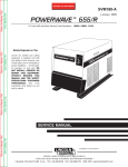
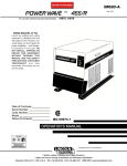
POWER WAVE 455/R
For use with machines having Code Numbers: 10675
10676
View Safety Info
Safety Depends on You
View Safety Info
Return to Master TOC
Return to Master TOC
Return to Master TOC
RETURN TO MAIN MENU
Lincoln arc welding and cutting
equipment is designed and built
with safety in mind. However,
your overall safety can be increased by proper installation . . .
and thoughtful operation on
your part. DO NOT INSTALL,
OPERATE OR REPAIR THIS
EQUIPMENT WITHOUT
READING THIS MANUAL AND
THE SAFETY PRECAUTIONS
CONTAINED THROUGHOUT.
And, most importantly, think
before you act and be careful.
PO
WE
RW
AV
E4
55
/R
/R
55
4
VE
WA
R
WE
PO
IO
N
O
OF
F
IEC 60974-1
View Safety Info
Return to Master TOC
SERVICE MANUAL
Copyright © 2001 Lincoln Global Inc.
• World's Leader in Welding and Cutting Products •
• Sales and Service through Subsidiaries and Distributors Worldwide •
Cleveland, Ohio 44117-1199 U.S.A. TEL: 216.481.8100 FAX: 216.486.1751 WEB SITE: www.lincolnelectric.com
Return to Master TOC
i
i
SAFETY
WARNING
CALIFORNIA PROPOSITION 65 WARNINGS
The engine exhaust from this product contains
Diesel engine exhaust and some of its constituents
chemicals known to the State of California to cause
are known to the State of California to cause cancancer, birth defects, or other reproductive harm.
cer, birth defects, and other reproductive harm.
The Above For Gasoline Engines
The Above For Diesel Engines
ARC WELDING can be hazardous. PROTECT YOURSELF AND OTHERS FROM POSSIBLE SERIOUS INJURY OR DEATH.
KEEP CHILDREN AWAY. PACEMAKER WEARERS SHOULD CONSULT WITH THEIR DOCTOR BEFORE OPERATING.
Return to Master TOC
Return to Master TOC
Read and understand the following safety highlights. For additional safety information, it is strongly recommended that you
purchase a copy of “Safety in Welding & Cutting - ANSI Standard Z49.1” from the American Welding Society, P.O. Box 351040,
Miami, Florida 33135 or CSA Standard W117.2-1974. A Free copy of “Arc Welding Safety” booklet E205 is available from the
Lincoln Electric Company, 22801 St. Clair Avenue, Cleveland, Ohio 44117-1199.
BE SURE THAT ALL INSTALLATION, OPERATION, MAINTENANCE AND REPAIR PROCEDURES ARE
PERFORMED ONLY BY QUALIFIED INDIVIDUALS.
FOR ENGINE
powered equipment.
1.a. Turn the engine off before troubleshooting and maintenance
work unless the maintenance work requires it to be running.
____________________________________________________
1.b.Operate engines in open, well-ventilated
areas or vent the engine exhaust fumes
outdoors.
____________________________________________________
1.c. Do not add the fuel near an open flame welding arc or when the engine is running. Stop
the engine and allow it to cool before refueling to prevent spilled fuel from vaporizing on
contact with hot engine parts and igniting. Do
not spill fuel when filling tank. If fuel is spilled,
wipe it up and do not start engine until fumes
have been eliminated.
____________________________________________________
1.d. Keep all equipment safety guards, covers
and devices in position and in good
repair.Keep hands, hair, clothing and tools
away from V-belts, gears, fans and all other
moving parts when starting, operating or
repairing equipment.
____________________________________________________
Return to Master TOC
1.h. To avoid scalding, do not remove the
radiator pressure cap when the engine is
hot.
1.e. In some cases it may be necessary to remove safety
guards to perform required maintenance. Remove
guards only when necessary and replace them when the
maintenance requiring their removal is complete.
Always use the greatest care when working near moving
parts.
___________________________________________________
1.f. Do not put your hands near the engine fan. Do not attempt to
override the governor or idler by pushing on the throttle control rods while the engine is running.
___________________________________________________
1.g. To prevent accidentally starting gasoline engines while
turning the engine or welding generator during maintenance
work, disconnect the spark plug wires, distributor cap or
magneto wire as appropriate.
ELECTRIC AND
MAGNETIC FIELDS
may be dangerous
2.a. Electric current flowing through any conductor causes
localized Electric and Magnetic Fields (EMF). Welding
current creates EMF fields around welding cables and
welding machines
2.b. EMF fields may interfere with some pacemakers, and
welders having a pacemaker should consult their physician
before welding.
2.c. Exposure to EMF fields in welding may have other health
effects which are now not known.
2.d. All welders should use the following procedures in order to
minimize exposure to EMF fields from the welding circuit:
2.d.1. Route the electrode and work cables together - Secure
them with tape when possible.
2.d.2. Never coil the electrode lead around your body.
2.d.3. Do not place your body between the electrode and
work cables. If the electrode cable is on your right
side, the work cable should also be on your right side.
2.d.4. Connect the work cable to the workpiece as close as
possible to the area being welded.
2.d.5. Do not work next to welding power source.
Mar ‘95
Return to Master TOC
Return to Master TOC
ii
ELECTRIC SHOCK can kill.
ARC RAYS can burn.
3.a. The electrode and work (or ground) circuits
are electrically “hot” when the welder is on.
Do not touch these “hot” parts with your bare
skin or wet clothing. Wear dry, hole-free
gloves to insulate hands.
4.a. Use a shield with the proper filter and cover
plates to protect your eyes from sparks and
the rays of the arc when welding or observing
open arc welding. Headshield and filter lens
should conform to ANSI Z87. I standards.
3.b. Insulate yourself from work and ground using dry insulation.
Make certain the insulation is large enough to cover your full
area of physical contact with work and ground.
4.b. Use suitable clothing made from durable flame-resistant
material to protect your skin and that of your helpers from
the arc rays.
In addition to the normal safety precautions, if welding
must be performed under electrically hazardous
conditions (in damp locations or while wearing wet
clothing; on metal structures such as floors, gratings or
scaffolds; when in cramped positions such as sitting,
kneeling or lying, if there is a high risk of unavoidable or
accidental contact with the workpiece or ground) use
the following equipment:
• Semiautomatic DC Constant Voltage (Wire) Welder.
• DC Manual (Stick) Welder.
• AC Welder with Reduced Voltage Control.
4.c. Protect other nearby personnel with suitable, non-flammable
screening and/or warn them not to watch the arc nor expose
themselves to the arc rays or to hot spatter or metal.
3.c. In semiautomatic or automatic wire welding, the electrode,
electrode reel, welding head, nozzle or semiautomatic
welding gun are also electrically “hot”.
3.d. Always be sure the work cable makes a good electrical
connection with the metal being welded. The connection
should be as close as possible to the area being welded.
3.e. Ground the work or metal to be welded to a good electrical
(earth) ground.
3.f. Maintain the electrode holder, work clamp, welding cable and
welding machine in good, safe operating condition. Replace
damaged insulation.
Return to Master TOC
ii
SAFETY
3.g. Never dip the electrode in water for cooling.
3.h. Never simultaneously touch electrically “hot” parts of
electrode holders connected to two welders because voltage
between the two can be the total of the open circuit voltage
of both welders.
3.i. When working above floor level, use a safety belt to protect
yourself from a fall should you get a shock.
3.j. Also see Items 6.c. and 8.
FUMES AND GASES
can be dangerous.
5.a. Welding may produce fumes and gases
hazardous to health. Avoid breathing these
fumes and gases.When welding, keep
your head out of the fume. Use enough
ventilation and/or exhaust at the arc to keep
fumes and gases away from the breathing zone. When
welding with electrodes which require special
ventilation such as stainless or hard facing (see
instructions on container or MSDS) or on lead or
cadmium plated steel and other metals or coatings
which produce highly toxic fumes, keep exposure as
low as possible and below Threshold Limit Values (TLV)
using local exhaust or mechanical ventilation. In
confined spaces or in some circumstances, outdoors, a
respirator may be required. Additional precautions are
also required when welding on galvanized steel.
5.b. Do not weld in locations near chlorinated hydrocarbon vapors
coming from degreasing, cleaning or spraying operations.
The heat and rays of the arc can react with solvent vapors to
form phosgene, a highly toxic gas, and other irritating
products.
5.c. Shielding gases used for arc welding can displace air and
cause injury or death. Always use enough ventilation,
especially in confined areas, to insure breathing air is safe.
5.d. Read and understand the manufacturer’s instructions for this
equipment and the consumables to be used, including the
material safety data sheet (MSDS) and follow your
employer’s safety practices. MSDS forms are available from
your welding distributor or from the manufacturer.
Return to Master TOC
5.e. Also see item 1.b.
Mar ‘95
Return to Master TOC
iii
WELDING SPARKS can
cause fire or explosion.
6.a. Remove fire hazards from the welding area.
If this is not possible, cover them to prevent
the welding sparks from starting a fire.
Remember that welding sparks and hot
materials from welding can easily go through small cracks
and openings to adjacent areas. Avoid welding near
hydraulic lines. Have a fire extinguisher readily available.
6.b. Where compressed gases are to be used at the job site,
special precautions should be used to prevent hazardous
situations. Refer to “Safety in Welding and Cutting” (ANSI
Standard Z49.1) and the operating information for the
equipment being used.
Return to Master TOC
6.c. When not welding, make certain no part of the electrode
circuit is touching the work or ground. Accidental contact can
cause overheating and create a fire hazard.
6.d. Do not heat, cut or weld tanks, drums or containers until the
proper steps have been taken to insure that such procedures
will not cause flammable or toxic vapors from substances
inside. They can cause an explosion even though they have
been “cleaned”. For information, purchase “Recommended
Safe Practices for the Preparation for Welding and Cutting of
Containers and Piping That Have Held Hazardous
Substances”, AWS F4.1 from the American Welding Society
(see address above).
6.e. Vent hollow castings or containers before heating, cutting or
welding. They may explode.
6.f. Sparks and spatter are thrown from the welding arc. Wear oil
free protective garments such as leather gloves, heavy shirt,
cuffless trousers, high shoes and a cap over your hair. Wear
ear plugs when welding out of position or in confined places.
Always wear safety glasses with side shields when in a
welding area.
Return to Master TOC
iii
SAFETY
6.g. Connect the work cable to the work as close to the welding
area as practical. Work cables connected to the building
framework or other locations away from the welding area
increase the possibility of the welding current passing
through lifting chains, crane cables or other alternate circuits.
This can create fire hazards or overheat lifting chains or
cables until they fail.
6.h. Also see item 1.c.
CYLINDER may explode
if damaged.
7.a. Use only compressed gas cylinders
containing the correct shielding gas for the
process used and properly operating
regulators designed for the gas and
pressure used. All hoses, fittings, etc. should be suitable for
the application and maintained in good condition.
7.b. Always keep cylinders in an upright position securely
chained to an undercarriage or fixed support.
7.c. Cylinders should be located:
• Away from areas where they may be struck or subjected to
physical damage.
• A safe distance from arc welding or cutting operations and
any other source of heat, sparks, or flame.
7.d. Never allow the electrode, electrode holder or any other
electrically “hot” parts to touch a cylinder.
7.e. Keep your head and face away from the cylinder valve outlet
when opening the cylinder valve.
7.f. Valve protection caps should always be in place and hand
tight except when the cylinder is in use or connected for
use.
7.g. Read and follow the instructions on compressed gas
cylinders, associated equipment, and CGA publication P-l,
“Precautions for Safe Handling of Compressed Gases in
Cylinders,” available from the Compressed Gas Association
1235 Jefferson Davis Highway, Arlington, VA 22202.
FOR ELECTRICALLY
powered equipment.
8.a. Turn off input power using the disconnect
switch at the fuse box before working on
the equipment.
8.b. Install equipment in accordance with the U.S. National
Electrical Code, all local codes and the manufacturer’s
recommendations.
8.c. Ground the equipment in accordance with the U.S. National
Electrical Code and the manufacturer’s recommendations.
Return to Master TOC
Mar ‘95
Return to Master TOC
Return to Master TOC
Return to Master TOC
Return to Master TOC
iv
iv
SAFETY
PRÉCAUTIONS DE SÛRETÉ
Pour votre propre protection lire et observer toutes les instructions
et les précautions de sûreté specifiques qui parraissent dans ce
manuel aussi bien que les précautions de sûreté générales suivantes:
Sûreté Pour Soudage A L’Arc
1. Protegez-vous contre la secousse électrique:
a. Les circuits à l’électrode et à la piéce sont sous tension
quand la machine à souder est en marche. Eviter toujours
tout contact entre les parties sous tension et la peau nue
ou les vétements mouillés. Porter des gants secs et sans
trous pour isoler les mains.
b. Faire trés attention de bien s’isoler de la masse quand on
soude dans des endroits humides, ou sur un plancher
metallique ou des grilles metalliques, principalement dans
les positions assis ou couché pour lesquelles une
grande partie du corps peut être en contact avec la
masse.
c. Maintenir le porte-électrode, la pince de masse, le câble
de soudage et la machine à souder en bon et sûr état
defonctionnement.
d. Ne jamais plonger le porte-électrode dans l’eau pour le
refroidir.
e. Ne jamais toucher simultanément les parties sous tension
des porte-électrodes connectés à deux machines à souder parce que la tension entre les deux pinces peut être le
total de la tension à vide des deux machines.
f. Si on utilise la machine à souder comme une source de
courant pour soudage semi-automatique, ces precautions
pour le porte-électrode s’applicuent aussi au pistolet de
soudage.
2. Dans le cas de travail au dessus du niveau du sol, se protéger contre les chutes dans le cas ou on recoit un choc. Ne
jamais enrouler le câble-électrode autour de n’importe quelle
partie du corps.
3. Un coup d’arc peut être plus sévère qu’un coup de soliel,
donc:
a. Utiliser un bon masque avec un verre filtrant approprié
ainsi qu’un verre blanc afin de se protéger les yeux du
rayonnement de l’arc et des projections quand on soude
ou quand on regarde l’arc.
b. Porter des vêtements convenables afin de protéger la
peau de soudeur et des aides contre le rayonnement de
l‘arc.
c. Protéger l’autre personnel travaillant à proximité au
soudage à l’aide d’écrans appropriés et non-inflammables.
4. Des gouttes de laitier en fusion sont émises de l’arc de
soudage. Se protéger avec des vêtements de protection
libres de l’huile, tels que les gants en cuir, chemise épaisse,
pantalons sans revers, et chaussures montantes.
5. Toujours porter des lunettes de sécurité dans la zone de
soudage. Utiliser des lunettes avec écrans lateraux dans les
zones où l’on pique le laitier.
6. Eloigner les matériaux inflammables ou les recouvrir afin de
prévenir tout risque d’incendie dû aux étincelles.
7. Quand on ne soude pas, poser la pince à une endroit isolé
de la masse. Un court-circuit accidental peut provoquer un
échauffement et un risque d’incendie.
8. S’assurer que la masse est connectée le plus prés possible
de la zone de travail qu’il est pratique de le faire. Si on place
la masse sur la charpente de la construction ou d’autres
endroits éloignés de la zone de travail, on augmente le risque
de voir passer le courant de soudage par les chaines de levage, câbles de grue, ou autres circuits. Cela peut provoquer
des risques d’incendie ou d’echauffement des chaines et des
câbles jusqu’à ce qu’ils se rompent.
9. Assurer une ventilation suffisante dans la zone de soudage.
Ceci est particuliérement important pour le soudage de tôles
galvanisées plombées, ou cadmiées ou tout autre métal qui
produit des fumeés toxiques.
10. Ne pas souder en présence de vapeurs de chlore provenant
d’opérations de dégraissage, nettoyage ou pistolage. La
chaleur ou les rayons de l’arc peuvent réagir avec les
vapeurs du solvant pour produire du phosgéne (gas fortement toxique) ou autres produits irritants.
11. Pour obtenir de plus amples renseignements sur la sûreté,
voir le code “Code for safety in welding and cutting” CSA
Standard W 117.2-1974.
PRÉCAUTIONS DE SÛRETÉ POUR
LES MACHINES À SOUDER À
TRANSFORMATEUR ET À
REDRESSEUR
1. Relier à la terre le chassis du poste conformement au code
de l’électricité et aux recommendations du fabricant. Le dispositif de montage ou la piece à souder doit être branché à
une bonne mise à la terre.
2. Autant que possible, I’installation et l’entretien du poste
seront effectués par un électricien qualifié.
3. Avant de faires des travaux à l’interieur de poste, la
debrancher à l’interrupteur à la boite de fusibles.
4. Garder tous les couvercles et dispositifs de sûreté à leur
place.
Mar. ‘93
v
- MASTER TABLE OF CONTENTS FOR ALL SECTIONS RETURN TO MAIN MENU
Page
Safety .................................................................................................................................................i-iv
Installation.............................................................................................................................Section A
Operation...............................................................................................................................Section B
Accessories ..........................................................................................................................Section C
Maintenance ..........................................................................................................................Section D
Theory of Operation .............................................................................................................Section E
Troubleshooting and Repair ................................................................................................Section F
Electrical Diagrams ..............................................................................................................Section G
Parts Manual ................................................................................................................................P-377
POWER WAVE 455/R
v
Return to Master TOC
Section A
TABLE OF CONTENTS
- INSTALLATION SECTION -
Installation.............................................................................................................................Section A
Technical Specifications ..............................................................................................................A-2
Safety Precautions ......................................................................................................................A-4
Select Suitable Location..............................................................................................................A-4
Lifting ....................................................................................................................................A-4
Stacking ................................................................................................................................A-4
Machine Grounding.....................................................................................................................A-4
High Frequency Protection..........................................................................................................A-4
Input Connection .........................................................................................................................A-5
Return to Master TOC
Input Fuse and Supply Wire Considerations ........................................................................A-5
Input Voltage Change Over (For Multiple Input Voltage Machines Only).............................A-6
Welding with Multiple Power Waves ...........................................................................................A-6
Electrode and Work Cable Connections .....................................................................................A-7
Negative Electrode Polarity.........................................................................................................A-7
Voltage Sensing ..........................................................................................................................A-8
Work Voltage Sensing ..........................................................................................................A-9
Electrode Voltage Sensing ...................................................................................................A-9
Power Wave / Power Feed Wire Feeder Interconnections.........................................................A-9
Control Cable Specifications ................................................................................................A-9
External I/O Connector .........................................................................................................A-9
Return to Master TOC
Return to Master TOC
Dip Switch Settings and Locations .....................................................................................A-10
Control Board Dip Switch ...................................................................................................A-10
Feed Head Board Dip Switch .............................................................................................A-10
Devicenet/Gateway Board Dip Switch, Bank (S2)..............................................................A-11
POWER WAVE 455/R
Section A
Return to Master TOC
A-2
INSTALLATION
TECHNICAL SPECIFICATIONS - POWER WAVE 455/R (K1761-1), (K1761-2)
INPUT AT RATED OUTPUT - THREE PHASE ONLY
INPUT
VOLTS
OUTPUT
CONDITIONS
INPUT
CURRENT
AMPS
(K1761-1)
208/230/460V - 60HZ
450A@38V 100%
570A@43V 60%
70/65/35
87/82/48
200/220/440V - 50HZ
400A@36V 100%
500A@40V 60%
64/58/32
79/74/41
(K1761-2)
208/230/460/575V-60HZ
450@38V 100%
570@43V 60%
58/53/25/22
82/78/37/31
200/220/440V - 50HZ
400@36V 100%
500A@40V 60%
49/45/23
67/61/31
IDLE
POWER
POWER FACTOR
EFFICIENCY
@ RATED OUTPUT @ RATED OUTPUT
0.89 MIN
400 Watts
MAX
88%
0.95 MIN
OUTPUT
Return to Master TOC
Return to Section TOC
Return to Section TOC
A-2
OPEN
CIRCUIT
VOLTAGE
75 VDC
PULSE
CURRENT
PULSE AND
PULSE
STT
AUXILIARY POWER
FREQUENCY VOLTAGE BACKGROUND PARAMETERS (CIRCUIT BREAKER
RANGE
TIME RANGE
RANGE
PROTECTED)
5 - 570
0.15 - 1000 Hz 5 - 55 VDC 100 MICRO SEC. 40-325 AMPS
-3.3 SEC.
PROCESS CURRENT RANGES (DC)
40 VDC @10 AMPS
115VAC @10 AMPS
CURRENT
MIG/MAG
FCAW
SMAW
Pulse
STT
50-570 Average Amps
40-570 Average Amps
30-570 Average Amps
5-750 Peak Amps
40-325 Average Amps
Return to Master TOC
Return to Master TOC
Return to Section TOC
Return to Section TOC
RECOMMENDED INPUT WIRE AND FUSE SIZES
INPUT
VOLTAGE /
FREQUENCY
(K1761-1)
208/230V - 60HZ
460V - 60HZ
200/220V - 50HZ
440V - 50HZ
208/230V - 60HZ
460V - 60HZ
200/220V - 50HZ
440V - 50HZ
(K1761-2)
208/230V - 60HZ
460V - 60HZ
575V - 60HZ
200/220V - 50HZ
440V - 50HZ
208/230V - 60HZ
460V - 60HZ
575V - 60HZ
200/220V - 50HZ
440V - 50HZ
AMPS/
DUTY
CYCLE
INPUT AMPERE
TYPE 75°C
TYPE 75°C
TYPE 75°C
RATING ON
COPPER WIRE GROUND WIRE (SUPER LAG)
IN CONDUIT
IN CONDUIT
OR BREAKER
NAMEPLATE
AWG[IEC] SIZES AWG[IEC] SIZES SIZE (AMPS)
(mm2)
(mm2)
450/100%
450/100%
400/100%
400/100%
570/60%
570/60%
500/60%
500/60%
70/65
35
64/58
32
87/82
48
79/74
41
4
8
4
8
4
8
4
8
(25)
(10)
(25)
(10)
(25)
(10)
(25)
(10)
8 (10)
10 (6)
8 (10)
10 (6)
6 (10)
10 (6)
8 (10)
10 (6)
90/90
45
90/80
45
110/110
70
100/100
60
450/100%
450/100%
450/100%
400/100%
400/100%
570/60%
570/60%
570/60%
500/60%
500/60%
58/53
25
22
49/45
23
82/78
37
31
67/61
31
4 (25)
10 (6)
10 (6)
6 (10)
10 (6)
4 (25)
8 (10)
10 (6)
8 (10)
10 (6)
8 (10)
10 (6)
10 (6)
8 (10)
10 (6)
6 (10)
10 (6)
10 (6)
8 (10)
10 (6)
70/60
35
30
70/60
30
110/100
50
40
90/80
40
Return to Master TOC
Return to Section TOC
A-3
A-3
INSTALLATION
TECHNICAL SPECIFICATIONS - POWER WAVE 455/R (K1761-1), (K1761-2)
(continued)
PHYSICAL DIMENSIONS
HEIGHT
WIDTH
DEPTH
26.10 in
663 mm
19.86 in
505 mm
32.88 in
835 mm
WEIGHT
(K1761-1) 247 lbs.
112 kg.
(K1761-2) 254 lbs.
115 kg.
TEMPERATURE RANGES
STORAGE TEMPERATURE RANGE
-40°C to +40°C
Return to Master TOC
Return to Master TOC
Return to Master TOC
Return to Section TOC
Return to Section TOC
Return to Section TOC
OPERATING TEMPERATURE RANGE
-20°C to +40°C
POWER WAVE 455/R
Return to Master TOC
Return to Section TOC
A-4
A-4
INSTALLATION
SAFETY PRECAUTIONS
CAUTION
Read this entire installation section before you
start installation.
WARNING
ELECTRIC SHOCK can kill.
DO NOT MOUNT OVER COMBUSTIBLE SURFACES.
Where there is a combustible surface directly under
stationary or fixed electrical equipment, that surface
shall be covered with a steel plate at least .06”(1.6mm)
thick, which shall extend not less than 5.90”(150mm)
beyond the equipment on all sides.
Return to Master TOC
Return to Section TOC
• Only qualified personnel should perform this installation.
• Turn the input power OFF at the disconnect switch or fuse box before working on this
equipment. Turn off the input power to any other equipment connected to the welding system at the disconnect switch or fuse box before working on the equipment.
LIFTING
• Do not touch electrically hot parts.
STACKING
• Always connect the Power Wave grounding lug
(located inside the reconnect input access door) to a
proper safety (Earth) ground.
Power Wave machines can be stacked a maximum of
three high.
CAUTION
SELECT SUITABLE LOCATION
Return to Master TOC
Return to Master TOC
Return to Section TOC
Do not use Power Waves in outdoor environments. The
Power Wave power source should not be subjected to
falling water, nor should any parts of it be submerged
in water. Doing so may cause improper operation as
well as pose a safety hazard. The best practice is to
keep the machine in a dry, sheltered area.
Return to Section TOC
Lift the machine by the lift bail only. The lift bail is
designed to lift the power source only. Do not attempt
to lift the Power Wave with accessories attached to it.
Place the welder where clean cooling air can freely circulate in through the rear louvers and out through the
case sides and bottom. Dirt, dust, or any foreign material that can be drawn into the welder should be kept at
a minimum. Do not use air filters on the air intake,
because the air flow will be restricted. Failure to
observe these precautions can result in excessive
operating temperatures and nuisance shutdowns.
Machines above code 10500 are equipped with F.A.N.
(fan as needed) circuitry. The fan runs whenever the
output is enabled, whether under loaded or open circuit
conditions. The fan also runs for a period of time
(approximately 5 minutes) after the output is disabled,
to ensure all components are properly cooled.
If desired, the F.A.N. feature can be disabled (causing
the fan to run whenever the power source is on). To disable F.A.N., connect leads 444 and X3A together at the
output of the solid state fan control relay, located on the
back of the Control PC board enclosure. (See the
Wiring Diagram.)
The bottom machine must always be placed on a firm,
secure, level surface. There is a danger of machines
toppling over if this precaution is not taken.
MACHINE GROUNDING
The frame of the welder must be grounded. A ground
terminal marked with the symbol
is located inside
the reconnect/input access door for this purpose. See
your local and national electrical codes for proper
grounding methods.
HIGH FREQUENCY PROTECTION
Locate the Power Wave away from radio controlled
machinery.
CAUTION
The normal operation of the Power Wave may adversely affect the operation of RF controlled equipment,
which may result in bodily injury or damage to the
equipment.
POWER WAVE 455/R
A-5
INSTALLATION
. Disconnect input power before
.
inspecting or servicing machine.
VOLTAGE=200-208V
W / L3
V / L2
200-208V
CR1
220-230V
U / L1
380-415V
Do not operate with covers
removed.
'A'
440-460V
ELECTRIC . Do not touch electrically live parts.
SHOCK
Only qualified persons should install,
CAN KILL
use or service this equipment.
.
VOLTAGE=220-230V
VOLTAGE=380-415V
200-208V
200-208V
200-208V
220-230V
220-230V
220-230V
380-415V
'A'
INPUT SUPPLY CONNECTION DIAGRAM
WARNING
WARNING
Disconnect input power before
inspecting or servicing machine.
Do not operate with covers
removed.
ELECTRIC
ELECTRIC
Do not touch electrically live parts.
SHOCK
SHOCK
Only qualified persons should install,
CAN KILL
CAN
KILL use or service this equipment.
Return to Master TOC
440-460V
VOLTAGE = 200-208V
W / L3
V / L2
200-208V
CR1
220-230V
U / L1
440-460V
VOLTAGE = 440-460V
VOLTAGE = 550-575V
200-208V
200-208V
200-208V
220-230V
220-230V
550-575V
'A'
'A'
550-575V
220-230V
440-460V
440-460V
'A'
550-575V
440-460V
'A'
550-575V
NOTE: Turn main input power to the machine OFF before performing connection procedure. Failure to do
so will result in damage to the machine.
INPUT FUSE AND SUPPLY WIRE
CONSIDERATIONS
INPUT CONNECTION
WARNING
Only a qualified electrician should connect the input
leads to the Power Wave. Connections should be made
in accordance with all local and national electrical codes
and the connection diagram located on the inside of the
reconnect/input access door of the machine. Failure to
do so may result in bodily injury or death.
Return to Master TOC
'A'
A
Return to Master TOC
Return to Section TOC
380-415V
(K1761-2) CONNECTION DIAGRAM ON CONNECTION/INPUT ACCESS DOOR
VOLTAGE = 220-230V
Return to Section TOC
'A'
380-415V
440-460V
440-460V
Return to Section TOC
VOLTAGE=440-460V
S23847
WARNING
THE LINCOLN ELECTRIC CO.
INPUT SUPPLY CONNECTION DIAGRAM
CLEVELAND, OHIO U.S.A.
FIGURE A.1
(K1761-1) CONNECTION DIAGRAM ON CONNECTION/INPUT ACCESS DOOR
THE LINCOLN ELECTRIC CO. CLEVELAND, OHIO U.S.A.
XA
S25198
Return to Master TOC
Return to Section TOC
A-5
Use a three-phase supply line. A 1.75 inch (45 mm)
diameter access hole for the input supply is located on
the upper left case back next to the input access door.
Connect L1, L2, L3 and ground according to the Input
Supply Connection Diagram decal located on the
inside of the input access door, or refer to Figure A.1.
Refer to the Technical Specifications at the beginning
of this Installation section for recommended fuse and
wire sizes. Fuse the input circuit with the recommended super lag fuse or delay type breakers (also called
“inverse time” or “thermal/magnetic” circuit breakers).
Choose an input and grounding wire size according to
local or national electrical codes. Using fuses or circuit
breakers smaller than recommended may result in
“nuisance” shut-offs from welder inrush currents, even
if the machine is not being used at high currents.
POWER WAVE 455/R
Return to Master TOC
Return to Master TOC
Return to Section TOC
Return to Section TOC
A-6
A-6
INSTALLATION
INPUT VOLTAGE CHANGE OVER
(FOR MULTIPLE INPUT VOLTAGE
MACHINES ONLY)
WELDING WITH MULTIPLE POWER
WAVES
CAUTION
Welders are shipped connected for the highest input
voltage listed on the rating plate. To move this connection to a different input voltage, see the diagram
located on the inside of the input access door. (Figure
A.1.) If the main reconnect switch or link position is
placed in the wrong position, the welder will not produce output power.
Special care must be taken when more than one Power
Wave is welding simultaneously on a single part. Arc
blow and arc interference may occur or be magnified.
If the Auxiliary (A) lead is placed in the wrong position,
there are two possible results. If the lead is placed in
a position higher than the applied line voltage, the
welder may not come on at all. If the auxiliary (A) lead
is placed in a position lower than the applied line voltage, the welder will not come on, and the two circuit
breakers in the reconnect area will open. If this occurs,
turn off the input voltage, properly connect the (A) lead,
reset the breakers, and try again.
Each power source requires a work lead from the work
terminal to the welding fixture. Do not combine all of the
work leads into one lead. The welding travel directions
should be in the direction moving away from the work
lead as shown in Figure A.2. Connect all of the work
sense leads from each power source to the work piece
at the end of the weld.
For the best results when pulse welding, set the wire
size and wire feed speed the same for all the Power
Waves.
FIGURE A.2 – MULTIPLE POWER WAVE CONNECTIONS
TWO POWER WAVES
I ON
I ON
Return to Master TOC
Return to Section TOC
POWERWAVE 455/R
POWERWAVE 455/R
O OFF
O OFF
SEN
SE L
EAD
ELECTRODE
ELECTRODE
VEL
TRAECTION
DIR
Return to Master TOC
Return to Section TOC
SENSE LEAD
CONNECT ALL WORK
SENSE LEADS AT THE
END OF THE JOINT
WORK LEAD
WORK LEAD
CONNECT ALL WELDING
WORK LEADS AT THE
BEGINNING OF THE JOINT
POWER WAVE 455/R
Return to Master TOC
Return to Section TOC
A-7
When these parameters are identical, the pulsing frequency will be the same, helping to stabilize the arcs.
Every welding gun requires a separate shielding gas
regulator for proper flow rate and shielding gas coverage.
Do not attempt to supply shielding gas for two or more
guns from only one regulator.
If an anti-spatter system is in use, each gun must have
its own anti-spatter system. See Figure A.2.
Return to Master TOC
Return to Section TOC
ELECTRODE AND WORK CABLE
CONNECTIONS
Connect a work lead of sufficient size and length (per
Table A.1) between the proper output terminal on the
power source and the work. Be sure the connection to
the work makes tight metal-to-metal electrical contact.
To avoid interference problems with other equipment
and to achieve the best possible operation, route all
cables directly to the work or wire feeder. Avoid excessive lengths and do not coil excess cable. Do not tightly bundle the electrode and work cables together.
Use K1796 coaxial welding cables wherever possible.
Return to Master TOC
Return to Section TOC
Minimum work and electrode cables sizes are as
follows:
TABLE A.1
(Current (60% Duty Cycle)
MINIMUM COPPER
WORK CABLE SIZE AWG
Up To 100 Ft. Length (30 m)
400 Amps
500 Amps
600 Amps
2/0 (67 mm )
3/0 (85 mm2)
3/0 (85 mm2)
Return to Master TOC
Most welding applications run with the electrode being
positive (+). For those applications, connect one end of
the electrode cable to the positive (+) output terminal
on the power source (located beneath the spring
loaded output cover near the bottom of the case front).
Connect the other end of the electrode cable to the
wire drive feed plate using the stud, lockwasher, and
nut provided on the wire drive feed plate. The electrode
cable lug must be against the feed plate. Be sure the
connection to the feed plate makes tight metal-to-metal
electrical contact. The electrode cable should be sized
according to the specifications given in Table A.1.
Connect a work lead from the negative (-) power
source output terminal to the work piece. The work
piece connection must be firm and secure, especially if
pulse welding is planned.
CAUTION
Excessive voltage drops caused by poor work piece
connections often result in unsatisfactory welding performance.
When welding with the STT process, use the positive
output connection labeled (STT) for STT welding. (If
desired, other welding modes can be used on this terminal; however, their average output current will be limited to 325 amps.) For non-STT processes, use the
positive output connection labeled (Power Wave), so
that the full output range of the machine is available.
CAUTION
2
When using an inverter type power source like the
Power Wave, use the largest welding (electrode and
ground) cables that are practical. At least 2/0 copper
wire - even if the average output current would not normally require it.
CAUTION
Return to Section TOC
A-7
INSTALLATION
When pulsing, the pulse current can reach very high
levels. Voltage drops can become excessive, leading
to poor welding characteristics, if undersized welding
cables are used.
Do not connect the STT and Power Wave terminals
together. Paralleling the terminals will bypass STT circuitry and severely deteriorate STT welding performance.
NEGATIVE ELECTRODE POLARITY
When negative electrode polarity is required, such as
in some Innershield applications, reverse the output
connections at the power source (electrode cable to
the negative (-) terminal, and work cable to the positive
(+) terminal).
When operating with electrode polarity negative, the
Dip switch 7 must be set to ON on the Wire Feed Head
PC Board. The default setting of the switch is OFF to
represent positive electrode polarity.
To set the Negative Polarity switch on Wire Feed Head
PC board, refer to the section DIP SWITCH
SETTINGS AND LOCATIONS.
POWER WAVE 455/R
Return to Master TOC
Return to Section TOC
A-8
VOLTAGE SENSING
The sense leads connect to the Power Wave at the
four-pin connector located underneath the output terminal cover. Lead 67 senses electrode voltage. Lead
21 senses work voltage.
The best arc performance occurs when the Power
Wave has accurate data about the arc conditions.
Depending upon the process, inductance within the
electrode and work lead cables can influence the voltage apparent at the terminals of the welder. Voltage
sense leads improve the accuracy of the arc conditions
and can have a dramatic effect on performance.
Enable the voltage sense leads as follows:
TABLE A.2
CAUTION
Return to Master TOC
If the voltage sensing is enabled but the sense leads
are missing or improperly connected, extremely high
welding outputs may occur.
Return to Section TOC
A-8
INSTALLATION
Do not tightly bundle the work sense lead to the work
lead.
Process
Electrode Voltage
Sensing 67 lead *
Work Voltage
Sensing 21 lead
GMAW
67 lead required
21 lead optional
GMAW-P 67 lead required
21 lead optional
FCAW
67 lead required
21 lead optional
STT
67 lead required
21 lead required
GTAW
Voltage sense at
terminals
Voltage sense at
terminals
SAW
67 lead required
21 lead optional
* The electrode voltage 67 sense lead is integral to the control cable to the wire feeder.
Return to Master TOC
Return to Master TOC
Return to Section TOC
Return to Section TOC
FIGURE A.3 – DIP SWITCH LOCATION
5/R
45
E
AV
RW
WE
O
P
REMOVE
FRONT
COVER
IO
N
O
OF
F
PO
WE
RW
AV
E4
55
/R
WIRE FEED
HEAD BOARD
ON RIGHT
POWER WAVE 455/R
CONTROL
BOARD
ON LEFT
WORK VOLTAGE SENSING
CONTROL CABLE SPECIFICATIONS
The Power Wave is shipped from the factory with the
work sense lead enabled.
It is recommended that genuine Lincoln control cables
be used at all times. Lincoln cables are specifically
designed for the communication and power needs of
the Power Wave / Power Feed system.
For processes requiring work voltage sensing, connect
the (21) work voltage sense lead from the Power Wave
to the work. Attach the sense lead to the work as close
to the weld as practical. To enable the work voltage
sensing in the Power Wave, refer to the section DIP
SWITCH SETTINGS AND LOCATIONS.
Enabling or disabling electrode voltage sensing is automatically configured through software. Electrode sense
lead 67 must be connected at the wire feeder.
CAUTION
The use of non-standard cables, especially in lengths
greater than 25 feet, can lead to communication problems (system shutdowns), poor motor acceleration
(poor arc starting) and low wire driving force (wire feeding problems).
Lincoln control cables are copper 22 conductor cable in
a SO-type rubber jacket.
3
4
5
6
7
8
9 10 11 12
Reserved for future use
2
Shutdown2 input
1
Shutdown1 input
A work lead must be run from the negative (-) power
source output connection to the work piece. The work
piece connection must be firm and secure, especially if
pulse welding is planned.
+15 for shutdown group
Output connections on some Power Waves are made
via 1/2-13 threaded output terminals located beneath
the spring-loaded output cover at the bottom of the
case front. On machines which carry the CE mark, output connections are made via Twist-Mate receptacles,
also located beneath the spring-loaded output cover at
the bottom of the case front.
Gas Purge Input
The Shutdown Group is always enabled. Shutdown 2 is
used for signaling low flow in the water cooler. Unused
shutdowns must be jumpered. Machines from the factory come with the shutdowns already jumpered. (See
Figure A.4)
FIGURE A.4 – INPUT PORT CONNECTIONS
Cold Inch Reverse
For convenience sake, the electrode and control
cables can be routed behind the left or right strain
reliefs (under the spring loaded output cover), and
along the channels formed into the base of the Power
Wave, out the back of the channels, and then to the
wire feeder.
Cold Inch Forward
The Power Wave is equipped with a port for making simple input signal connections. The port is divided into
three groups: Trigger group, Cold Inch Group and
Shutdown Group. Because the Power Wave is a “slave”
on the DeviceNet network, the Trigger and Cold Inch
Groups are disabled when the DeviceNet/Gateway is
active.
+15 VDC for Cold Inch Group
Connect the control cable between the power source
and wire feeder. The wire feeder connection on the
robotic Power Wave is located under the spring loaded
output cover, near the bottom of the case front. The
control cable is keyed and polarized to prevent improper connection.
4 Step Input
EXTERNAL I/O CONNECTOR
Dual Procedure Input
POWER WAVE / POWER FEED WIRE
FEEDER INTERCONNECTIONS
Trigger Input
Return to Master TOC
Return to Master TOC
Return to Section TOC
ELECTRODE VOLTAGE SENSING
Return to Section TOC
A-9
INSTALLATION
+15 VDC for Trigger Group
Return to Master TOC
Return to Section TOC
A-9
Return to Master TOC
Return to Section TOC
CAUTION
Excessive voltage drops at the work piece connection
often result in unsatisfactory pulse welding performance.
A
D
B
E
C
POWER WAVE 455/R
G
H
F
I
Return to Master TOC
Return to Section TOC
A-10
A-10
INSTALLATION
DIP SWITCH SETTINGS AND LOCATIONS
CONTROL BOARD DIP SWITCH:
DIP switches on the PC boards allow for custom configuration of the Power Wave. Access the DIP switches as follows:
switch
switch
switch
switch
switch
switch
switch
switch
WARNING
ELECTRIC SHOCK CAN KILL.
1
2
3
4
5
6
7
8
=
=
=
=
=
=
=
=
reserved for future
reserved for future
reserved for future
reserved for future
reserved for future
reserved for future
reserved for future
work sense lead
use
use
use
use
use
use
use
• Do not touch electrically live parts or
electrodes with your skin or wet clothing.
Return to Master TOC
Return to Section TOC
• Insulate yourself from the work and
ground.
switch 8
work sense lead
off
work sense lead not connected
on
work sense lead connected
• Always wear dry insulating gloves.
FEED HEAD BOARD DIP SWITCH:
• Turn off power at the disconnect switch.
switch
switch
switch
switch
switch
switch
switch
switch
• Remove the top four screws securing the front access
panel.
• Loosen, but do not completely remove, the bottom
two screws holding the access panel.
Return to Master TOC
Return to Section TOC
• Open the access panel, allowing the weight of the
panel to be carried by the bottom two screws. Make
sure to prevent the weight of the access panel from
hanging on the harness.
• Adjust the DIP switches as necessary. Using a pencil or other small object, slide the switch left for the
ON position or to the right for the OFF position, as
appropriate.
Return to Master TOC
=
=
=
=
=
=
=
=
reserved for future use
reserved for future use
reserved for future use
reserved for future use
reserved for future use
reserved for future use
negative polarity switch
high speed gear
switch 7
electrode polarity
off
positive
on
negative
switch 8
wire drive gear
off
low speed gear
on
high speed gear
• Replace the panel and screws and restore power.
CONTROL BOARD
(LOCATED IN
CONTROL BOX
BEHIND CASE
FRONT)
DEVICENET/
GATEWAY
BOARD
(LOCATED
BEHIND
FRONT
COVER)
FRONT
COVER
Return to Section TOC
1
2
3
4
5
6
7
8
LEFT
BANK S1
FEED HEAD
BOARD
(LOCATED IN
CONTROL
BOX BEHIND
CASE FRONT)
CASE FRONT
BANK S2
OPENING IN
CASE FRONT
TO ACCESS
CONTROL
BOX
RIGHT
POWER WAVE 455/R
Return to Master TOC
Return to Master TOC
Return to Section TOC
Return to Section TOC
A-11
INSTALLATION
DEVICENET/GATEWAY BOARD
DIP SWITCH, BANK (S2):
switch 1,2 = configure the baud rate
for DeviceNET
Prior to S24958-6 software
switch 1
switch 2
baud rate
off
off
-------
on
off
125K
off
on
250K
on
on
500
S24958-6 and later software
switch 1
switch 2
baud rate
off
off
125K
off
on
250K
on
off
500K
on
on
500K
Return to Section TOC
Return to Master TOC
Return to Section TOC
Return to Master TOC
Programmable value. Consult local Lincoln Technical
representative.
switch
switch
switch
switch
5
6
7
8
=
=
=
=
reserved
reserved
reserved
reserved
for
for
for
for
future
future
future
future
use
use
use
use
POWER WAVE 455/R
A-11
Return to Section TOC
Return to Master TOC
Return to Section TOC
Return to Master TOC
Return to Master TOC
Return to Section TOC
Return to Master TOC
Return to Section TOC
A-12
NOTES
POWER WAVE 455/R
A-12
Return to Master TOC
Section B-1
TABLE OF CONTENTS
- OPERATION SECTION -
Section B-1
Operation...............................................................................................................................Section B
Safety Precautions ......................................................................................................................B-2
Graphic Symbols.........................................................................................................................B-3
General Description ....................................................................................................................B-4
Design Features and Advantages ........................................................................................B-4
Recommended Processes and Equipment.................................................................................B-5
Recommended Processes....................................................................................................B-5
Recommended Equipment ...................................................................................................B-5
Required Equipment .............................................................................................................B-5
Duty Cycle and Time Period.................................................................................................B-5
Case Front Controls ....................................................................................................................B-6
Welding Mode Descriptions ........................................................................................................B-7
Constant Voltage Welding ....................................................................................................B-7
Pulse Welding.......................................................................................................................B-8
STT Welding .........................................................................................................................B-9
Return to Master TOC
Return to Master TOC
Return to Master TOC
Limitations.............................................................................................................................B-5
POWER WAVE 455/R
Return to Master TOC
Return to Section TOC
B-2
OPERATION
SAFETY PRECAUTIONS
Read this entire section of operating instructions
before operating the machine.
WARNING
Return to Master TOC
Return to Section TOC
ELECTRIC SHOCK can kill.
• Unless using cold feed feature, when
feeding with gun trigger, the electrode and
drive mechanism are always electrically
energized and could remain energized
several seconds after the welding ceases.
• Do not touch electrically live parts or electrodes with
your skin or wet clothing.
• Insulate yourself from the work and ground.
• Always wear dry insulating gloves.
FUMES AND GASES can be
dangerous.
• Keep your head out of fumes.
Return to Master TOC
Return to Section TOC
• Use ventilation or exhaust to remove
fumes from breathing zone.
WELDING SPARKS can cause
fire or explosion.
• Keep flammable material away.
• Do not weld on containers that have held
combustibles.
ARC RAYS can burn.
Return to Master TOC
Return to Section TOC
• Wear eye, ear, and body protection.
Observe additional guidelines detailed in the beginning
of this manual.
POWER WAVE 455/R
B-2
Return to Master TOC
Return to Master TOC
Return to Master TOC
Return to Section TOC
Return to Section TOC
Return to Section TOC
B-3
B-3
OPERATION
GRAPHIC SYMBOLS THAT APPEAR ON
THIS MACHINE OR IN THIS MANUAL
INPUT POWER
SMAW
ON
GMAW
OFF
FCAW
HIGH TEMPERATURE
GTAW
MACHINE STATUS
U0
OPEN CIRCUIT VOLTAGE
CIRCUIT BREAKER
U1
INPUT VOLTAGE
WIRE FEEDER
U2
OUTPUT VOLTAGE
POSITIVE OUTPUT
I1
INPUT CURRENT
NEGATIVE OUTPUT
I2
OUTPUT CURRENT
3 PHASE INVERTER
PROTECTIVE
GROUND
INPUT POWER
WARNING OR
CAUTION
Return to Master TOC
Return to Section TOC
THREE PHASE
DIRECT CURRENT
POWER WAVE 455/R
Return to Master TOC
Return to Master TOC
Return to Master TOC
Return to Master TOC
Return to Section TOC
Return to Section TOC
Return to Section TOC
Return to Section TOC
B-4
OPERATION
B-4
GENERAL DESCRIPTION
DESIGN FEATURES AND ADVANTAGES
The Power Wave power source is designed to be a part
of a modular, multi-process welding system.
Depending on configuration, it can support constant
current, constant voltage, Surface Tension Transfer
and pulse welding modes.
• Designed to the IEC 974-1 Standard.
The Power Wave power source is designed to be used
with the family of Power Feed wire feeders, operating
as a system. Each component in the system has special circuitry to “talk with” the other system components, so each component (power source, wire feeder,
electrical accessories) knows what the other is doing at
all times. The components communicate using ArcLink
protocol.
Robotic systems can communicate with other industrial machines via DeviceNET protocol. The result is a
highly intrigated and flexible welding cell.
The Power Wave 455/R is a high performance, digitally controlled inverter welding power source capable of
complex, high-speed waveform control. Properly
equipped, it can support the GMAW, GMAW-P, FCAW,
GTAW and STT processes. It carries an output rating of
either 450 amps, 38 volts; or 400 amps, 36 volts (both
at 100% duty cycle), depending on input voltage and
frequency. The Surface Tension transfer process (STT)
is supported at currents up to 325 amps, at 100% duty
cycle.
• Power Wave 455 multiple process output ranges:
5 - 570 amps
• Easy access for input connections. Connections are
simple strip and clamp (no lugs required).
• F.A.N. (Fan As Needed). Cooling fan runs only when
necessary (above Code 10500 only, and all STT
machines).
• Modular construction for easy servicing.
• Thermostatically protected.
• Electronic over-current protection.
• Input over-voltage protection.
• Utilizes digital signal processing and microprocessor
control.
• Simple, reliable input voltage change over.
• All system components communicate and transfer
information.
• Auto device recognition simplifies accessory cable
connections.
If the duty cycle is exceeded, a thermostat will shut off
the output until the machine cools to a reasonable
operating temperature.
POWER WAVE 455/R
Return to Master TOC
Return to Master TOC
Return to Master TOC
Return to Master TOC
Return to Section TOC
Return to Section TOC
Return to Section TOC
Return to Section TOC
B-5
OPERATION
RECOMMENDED PROCESSES
AND EQUIPMENT
B-5
REQUIRED EQUIPMENT
• PF-10/R Wire Feeder, K1780-1
• Control Cables (22 pin to 22 pin), K1795-10,-25,-50,100
RECOMMENDED PROCESSES
The Power Wave 455/R can be set up in a number of
configurations, some requiring optional equipment or
welding programs. Each machine is factory preprogrammed with multiple welding procedures, typically
including GMAW, GMAW-P, FCAW, GTAW and STT
for a variety of materials, including mild steel, stainless
steel, cored wires, and aluminum. The STT process
supports mild steel and stainless steel welding.
• Control Cables (for use on FANUC robot arm, 22 pin
to 14 pin, 10 ft), K1804-1
The Power Wave 455/R is recommended only for
automatic or mechanized applications such as robotic
welding.
LIMITATIONS
RECOMMENDED EQUIPMENT
• Power Waves are not to be used in outdoor environments.
Automatic Operation
All welding programs and procedures are set through
software for the robotic Power Wave. FANUC robots
equipped with RJ-3 controllers may communicate
directly with the Power Wave. Other pieces of equipment such as PLCs or computers can communicate
with the Power Wave using DeviceNET. All wire welding processes require a robotic Power Feed wire feeder.
• Control Cables (for use on FANUC robot arm, 22 pin
to 14 pin, 18 in), K1805-1
• Control Cables (for use on FANUC robot arm, 22 pin
to 14 pin, 18 in), K1804-2
• The Power Wave 455/R is not suitable for SMAW,
CAC-A or other processes not listed.
• Only ArcLink Power Feed wire feeders and user
interfaces may be used. Other Lincoln wire feeders
or non-Lincoln wire feeders cannot be used.
DUTY CYCLE AND TIME PERIOD
The Power Feed wire feeders are capable of welding at
a 100% duty cycle (continuous welding). The power
source will be the limiting factor in determining system
duty cycle capability. Note that the duty cycle is based
upon a ten minute period. A 60% duty cycle represents
6 minutes of welding and 4 minutes of idling in a ten
minute period.
POWER WAVE 455/R
Return to Master TOC
Return to Section TOC
B-6
CASE FRONT CONTROLS
3. HIGH TEMPERATURE LIGHT (thermal overload):
A yellow light that comes on when an over temperature situation occurs. Output is disabled until
the machine cools down. When cool, the light
goes out and output is enabled.
All operator controls and adjustments are located on
the case front of the Power Wave. (See Figure B.1)
1. POWER SWITCH: Controls input power to the
Power Wave.
2. STATUS LIGHT: A two color light that indicates system errors. Normal operation is a steady green
light. Error conditions are indicated, per Table B.1.
4. 10 AMP WIRE FEEDER CIRCUIT BREAKER:
Protects 40 volt DC wire feeder power supply.
5. 10 AMP AUXILIARY POWER CIRCUIT BREAKER:
Protects 115 volt AC case front receptacle auxiliary supply.
Return to Master TOC
Return to Section TOC
NOTE: The robotic Power Waves’ status light will flash
green, and sometimes red and green, for up to
one minute when the machine is first turned on.
This is a normal situation as the machine goes
through a self test at power up.
Return to Master TOC
6. LEAD CONNECTOR S2 (SENSE LEAD)
7. 5-PIN ARC LINK S1
TABLE B.1
Light
Condition
8. 5-PIN DEVICENET CONNECTOR S5
9. I / O CONNECTOR
Meaning
Steady
Green
System OK. Power source
communicating normally with
wire feeder and its components.
Blinking
Green
Normal for first 1-10 seconds
after power is turned on.
Alternating
Green
and Red
Return to Section TOC
B-6
OPERATION
Steady
Red
10. NEGATIVE OUTPUT TERMINAL
11. INTERFACE CONNECTOR S6
12. STT TERMINAL
13. POSITIVE OUTPUT TERMINAL
14. AUXILIARY OUTPUT
Non-recoverable system fault.
Must turn power source off, find
source of error, and turn power
back on to reset. See
Troubleshooting Guide.
See Troubleshooting Guide.
FIGURE B.1 – POWER WAVE CASE FRONT CONTROLS
2
I ON
6
POWERWAVE 455/R
3
1
O OFF
7
Return to Master TOC
Return to Section TOC
8
9
11
10
12
13
5
14
4
POWER WAVE 455/R
Return to Section TOC
Return to Master TOC
Return to Section TOC
Return to Master TOC
Return to Section TOC
Return to Master TOC
B-7
OPERATION
WELDING MODE DESCRIPTIONS
CONSTANT VOLTAGE WELDING
For each wire feed speed, a corresponding voltage is
preprogrammed into the machine through special software at the factory. The preprogrammed voltage is the
best average voltage for a given wire feed speed. With
synergic programs, when the wire feed speed changes,
the Power Wave will automatically adjust the corresponding voltage.
Wave control adjusts the inductance of the waveshape.
(This adjustment is often referred to as "pinch". Inductance is inversely proportional to pinch.) Increasing
wave control greater than 0 results in a harsher, colder
arc, while decreasing the wave control to less than 0
provides a softer, hotter arc. (See Figure B.2.)
FIGURE B.2 – CV WAVE CONTROL CHARACTERISTICS
Wave Control +10.0
Wave Control 0.00
Wave Control -10.0
Current
Return to Master TOC
Time
Return to Section TOC
B-7
POWER WAVE 455/R
Return to Master TOC
Return to Master TOC
Return to Section TOC
Return to Section TOC
B-8
OPERATION
PULSE WELDING
Pulse welding procedures are set by controlling an
overall “arc length” variable. When pulse welding, the
arc voltage is highly dependent upon the waveform.
The peak current, background current, rise time, fall
time and pulse frequency all affect the voltage. The
exact voltage for a given wire feed speed can only be
predicted when all the pulsing waveform parameters
are known. Using a preset voltage becomes impractical, and instead the arc length is set by adjusting “trim.”
The Power Wave utilizes “adaptive control” to compensate for changes in electrical stick-out while welding.
(Electrical stick-out is the distance from the contact tip
to the work piece.) The Power Wave waveforms are
optimized for a 0.75" (19mm) stick-out. The adaptive
behavior supports a range of stickouts from 0.50"
(13mm) to 1.25" (32mm). At very low or high wire feed
speeds, the adaptive range may be less due to reaching the physical limitations of the welding process.
Trim adjusts the arc length and ranges from 0.50 to
1.50, with a nominal value of 1.00. Trim values greater
than 1.00 increase the arc length, while values less
than 1.00 decrease the arc length.
Wave control in pulse programs usually adjusts the
focus or shape of the arc. Wave control values greater
than 0 increase the pulse frequency while decreasing
the background current, resulting in a tight, stiff arc
best for high speed sheet metal welding. Wave control
values less than 0 decrease the pulse frequency while
increasing the background current for a soft arc good
for out-of-position welding. (See Figure B.3.)
Most pulse welding programs are synergic. As the wire
feed speed is adjusted, the Power Wave will automatically recalculate the waveform parameters to maintain
similar arc properties.
Return to Master TOC
Return to Section TOC
FIGURE B.3 – PULSE WAVE CONTROL CHARACTERISTICS
Current
Wave Control -10.0
Wave Control 0.00
Wave Control +10.0
Return to Master TOC
Time
Return to Section TOC
B-8
POWER WAVE 455/R
Return to Master TOC
Return to Section TOC
B-9
B-9
OPERATION
STT WELDING
The pictures illustrate the waveshape of current for the
process. They are not drawn to scale, and are intended only for the purpose of showing how the variables
affect the waveform.
Trim in the STT mode adjusts the tailout and background portion of the waveform. Trim values greater
than 1.0 add more energy to the weld and make the
weld puddle hotter; trim values less than 1.0 reduce
energy to weld. A nominal value of 1.0 will work for
most applications. (See Figure B.4.)
Return to Master TOC
Return to Master TOC
Return to Section TOC
Return to Section TOC
FIGURE B.4 – STT TRIM CONTROL CHARACTERISTICS
Trim 1.50
Current
Trim 1.00
Time
Trim 0.50
For most programs, peak current is adjusted by wave
control values. A value of +10.0 maximizes the peak
current, while a wave control of -10.0 minimizes peak
current. In general, the peak current is proportional to
torch arc length. (See Figure B.5.)
NOTE: The ranges on Wave Control and Trim are
dependent on the weld programs. The values
shown are typical ranges.
FIGURE B.5 – STT WAVE CONTROL CHARACTERISTICS
Wave Control +10.0
Wave Control 0.00
Wave Control -10.0
Return to Master TOC
Return to Section TOC
Current
Time
POWER WAVE 455/R
Return to Section TOC
Return to Master TOC
Return to Section TOC
Return to Master TOC
Return to Master TOC
Return to Section TOC
Return to Master TOC
Return to Section TOC
B-10
NOTES
POWER WAVE 455/R
B-10
TABLE OF CONTENTS
- ACCESSORIES SECTION -
Optional Equipment ....................................................................................................................C-2
Factory Installed ...................................................................................................................C-2
Field Installed .......................................................................................................................C-2
Return to Master TOC
Return to Master TOC
Section C-1
Accessories ..........................................................................................................................Section C
Return to Master TOC
Return to Master TOC
Section C-1
POWER WAVE 455/R
Return to Master TOC
Return to Section TOC
C-2
Return to Master TOC
Return to Master TOC
Return to Master TOC
Return to Section TOC
Return to Section TOC
C-2
OPTIONAL EQUIPMENT
FACTORY INSTALLED
There are no factory installed options available for the
Power Wave 455R.
The water cooler is designed to cool only one welding
gun and should be not used to cool multiple guns or
other devices.
FIELD INSTALLED
•
Return to Section TOC
ACCESSORIES
Gas Guard Regulator (K659-1)
The Gas Guard regulator is available as an optional accessory for the Power Feed Robotic wire drive
unit. Install the 5/8-18 male outlet on the regulator
to the proper 5/8-18 female gas inlet on the back
panel of the wire drive. Secure the fitting with the
flow adjuster key at the top.
•
Voltage Sense Leads (K940-10, -25 or -50)
The voltage sense leads connect at the front of the
machine. (See Figure A.2.)
•
Power Wave Water Cooler (K1767-1)*
The K1767-1 is the recommended water cooler for
the Power Wave. Incorporated into the cooler is an
automatic flow sensor to detect low coolant flow. In
the event of a low flow condition, a fault signal is
sent to the Power Wave, and welding output automatically stops to protect the torch.
Water cooler manufacturers often specify additives
to the coolant such as fungicides or alkalies. Follow
the manufacturers’ recommendations to achieve
proper operation and long lifetime without clogging.
•
Water Flow Sensor (K1536-1)
Water cooled guns can be damaged very quickly if
they are used even momentarily without water flowing. Recommend practice is to install a water flow
sensor such as on the water return line of the torch.
When fully integrated into the welding system, the
sensor will prevent welding if no water flow is present.
•
Dual Cylinder Undercarriage, K1570-1*
•
Coaxial Welding Cable, K1796
*The Dual Cylinder Undercarriage, K1570-1, is not
compatible in combination with the Power Wave
Water Cooler K1767-1.
POWER WAVE 455/R
TABLE OF CONTENTS
- MAINTENANCE SECTION -
Safety Precautions......................................................................................................................D-2
Routine and Periodic Maintenance.............................................................................................D-2
Main Assembly (Exploded View) ...............................................................................................D-3
Return to Master TOC
Return to Master TOC
Section D-1
Maintenance ..........................................................................................................................Section D
Return to Master TOC
Return to Master TOC
Section D-1
POWER WAVE 455/R
Return to Master TOC
Return to Section TOC
D-2
MAINTENANCE
PERFORM THE FOLLOWING DAILY:
SAFETY PRECAUTIONS
1. Check that no combustible materials are in the
welding or cutting area or around the machine.
WARNING
2. Remove any debris, dust, dirt, or materials that
could block the air flow to the machine for cooling.
ELECTRIC SHOCK can kill.
• Only Qualified personnel should
perform this maintenance.
• Turn the input power OFF at the
disconnect switch or fuse box
before working on this equipment.
Return to Master TOC
Return to Section TOC
•
D-2
Do not touch electrically hot parts.
3. Inspect the electrode cables for any slits or punctures in the cable jacket, or any condition that
would affect the proper operation of the machine.
PERFORM PERIODICALLY:
Clean the inside of the machine with a low pressure air
stream. Clean the following parts. Refer to Figure
D.1.
• Transformer and output rectifier assembly.
ROUTINE AND PERIODIC
MAINTENANCE
• Electrode and work cable connections.
• PC board connections..
1. Disconnect input AC power supply lines to the
machine before performing periodic maintenance,
tightening, cleaning, or replacing parts. See
Figure D.1.
• Intake and outlet louvers on the machine case.
• Any obvious accumulations of dirt within the
machine.
• Fan Assembly.
Return to Section TOC
Return to Master TOC
Return to Section TOC
Return to Master TOC
NOTE: The fan motor has sealed bearings which
require no maintenance.
POWER WAVE 455/R
D-3
MAINTENANCE
Return to Master TOC
Return to Section TOC
D-3
FIGURE D.1 – MAIN ASSEMBLY (EXPLODED VIEW)
7
7
1
Return to Master TOC
Return to Section TOC
7
3
Return to Master TOC
Return to Section TOC
4
2
2
6
5
1. CASE FRONT ASSEMBLY
2. TRANSFORMER AND OUTPUT
RECTIFIER ASSEMBLY
3. INPUT ASSEMBLY
Return to Master TOC
Return to Section TOC
4. CONTROL BOX AND VERTICAL
DIVIDER ASSEMBLY
2
5. BASE, LIFT BAIL AND FAN
ASSEMBLY
6. SWITCH BOARD HEATSINK
ASSEMBLY
7. CASE PARTS
POWER WAVE 455/R
Return to Section TOC
Return to Master TOC
Return to Section TOC
Return to Master TOC
Return to Master TOC
Return to Section TOC
Return to Master TOC
Return to Section TOC
D-4
NOTES
POWER WAVE 455/R
D-4
Return to Master TOC
Section E-1
Section E-1
TABLE OF CONTENTS
- THEORY OF OPERATION SECTION -
Theory of Operation .............................................................................................................Section E
General Description ....................................................................................................................E-2
Input Voltage and Precharge ......................................................................................................E-3
Switch Boards and Main Transformer.........................................................................................E-4
DC Bus Board, Power Board, Feed Head Board, Gateway Board
and Voltage Sense Board ...........................................................................................................E-5
Control Board ..............................................................................................................................E-7
Output Rectifier, Output Choke and STT Chopper Board ..........................................................E-8
Return to Master TOC
Thermal Protection, Protective Circuits, Over Current Protection
and Under/Over Voltage Protection ............................................................................................E-9
General Description of STT (Surface Tension Transfer) Process.............................................E-10
Insulated Gate Bipolar Transistor (IGBT) Operation .................................................................E-11
Pulse Width Modulation ............................................................................................................E-12
FIGURE E.1 – BLOCK LOGIC DIAGRAM
IGBT DRIVE
FROM
CONTROL
BOARD
POWER WAVE 455/R
INPUT
RECTIFIER
Return to Master TOC
+20 VDC FROM
POWER BOARD
IGBT DRIVE
FROM
CONTROL CT CURRENT
TO CONTROL
BOARD
BOARD
SW1
CURRENT
TRANSDUCER
STT CHOPPER
BOARD
STT
ELECTRODE
TERMINAL
+
RIGHT
SWITCH
BOARD
CAP. V/F
FEEDBACK
ELECTRODE
TERMINAL
+
LEFT
SWITCH
BOARD
RECONNECT
SWITCH
STT
DRIVE
CURRENT
TRANSDUCER
OUTPUT
CHOKE
WORK
TERMINAL
67A
INPUT
BOARD
S1
67B
CONTACTOR AND PRECHARGE
CONTROL SIGNALS FROM
CONTROL BOARD
AUX
RECONNECT
MAIN
TRANSFORMER
OUTPUT DIODES
D1 -D4
CAP. V/F
FEEDBACK
CR1
CT CURRENT
TO CONTROL
BOARD
S6
VOLT
SENSE
BOARD
VOLTAGE SENSE
OUTPUT
VOLTAGE SENSE SELECT
ARC LINK
2
4
V
A
C
FROM CONTROL
BOARD
FEED
HEAD
BOARD
40 VDC
115 VAC
FAN
RELAY
DEVICE NET
S5
GATEWAY
BOARD
CONNECTION
TO
ROBOT
TO
LEFT
S.B.
TO
RIGHT
S.B.
C
U
R
R
E
N
T
F
B
S
T
T
F
B
40 VDC
TO FAN RELAY
IGBT
DRIVES
CONTACTOR AND
PRECHARGE
CONTROL SIGNALS
ARC LINK
115 VAC
+5V RS232
65 VDC
52 VAC
Return to Master TOC
DC
BUS
BOARD
BUS BOARD
RECTIFIER
T1
230 VAC
WATER
COOLER
S6
CONNECTION
TO WIRE
DRIVE
+5 V ARC LINK
POWER
BOARD
40 VDC
T2
115 VAC
S2 WORK
SENSE
+15V SPI
40 VDC
S3
RS232
+5 V
+15 V
-15 V
40 VDC
115 VAC
RECP.
+5V SPI
THERMOSTATS
CONTROL
BOARD
S1
ARC LINK
WIRE
FEEDER
RECP.
POWER WAVE 455/R
LEFT S.B.
CAP. V/F
RIGHT S.B.
CAP. V/F
+20 VDC
TO
CHOPPER
BOARD
LEFT CT
CURRENT
FB
RIGHT CT
CURRENT
FB
STATUS
LIGHT
THERMAL
LIGHT
Return to Master TOC
Return to Section TOC
E-2
FIGURE E.2 – INPUT VOLTAGE AND PRECHARGE
IGBT DRIVE
FROM
CONTROL
BOARD
POWER WAVE 455/R
INPUT
RECTIFIER
Return to Master TOC
+20 VDC FROM
POWER BOARD
IGBT DRIVE
FROM
CONTROL CT CURRENT
TO CONTROL
BOARD
BOARD
SW1
CURRENT
TRANSDUCER
STT CHOPPER
BOARD
STT
ELECTRODE
TERMINAL
+
RIGHT
SWITCH
BOARD
CAP. V/F
FEEDBACK
ELECTRODE
TERMINAL
+
LEFT
SWITCH
BOARD
RECONNECT
SWITCH
STT
DRIVE
CURRENT
TRANSDUCER
OUTPUT
CHOKE
WORK
TERMINAL
67A
INPUT
BOARD
S1
67B
CONTACTOR AND PRECHARGE
CONTROL SIGNALS FROM
CONTROL BOARD
AUX
RECONNECT
MAIN
TRANSFORMER
CT CURRENT
TO CONTROL
BOARD
OUTPUT DIODES
D1 -D4
CAP. V/F
FEEDBACK
CR1
Return to Section TOC
E-2
THEORY OF OPERATION
S6
VOLT
SENSE
BOARD
VOLTAGE SENSE
OUTPUT
DEVICE NET
S5
VOLTAGE SENSE SELECT
ARC LINK
2
4
V
A
C
FROM CONTROL
BOARD
FEED
HEAD
BOARD
40 VDC
115 VAC
FAN
RELAY
GATEWAY
BOARD
CONNECTION
TO
ROBOT
TO
LEFT
S.B.
TO
RIGHT
S.B.
C
U
R
R
E
N
T
F
B
S
T
T
F
B
40 VDC
TO FAN RELAY
IGBT
DRIVES
CONTACTOR AND
PRECHARGE
CONTROL SIGNALS
ARC LINK
115 VAC
+5V RS232
65 VDC
52 VAC
230 VAC
S6
DC
BUS
BOARD
BUS BOARD
RECTIFIER
T1
CONNECTION
TO WIRE
DRIVE
Return to Master TOC
Return to Master TOC
Return to Section TOC
Return to Section TOC
115 VAC
+5V SPI
THERMOSTATS
CONTROL
BOARD
S2 WORK
SENSE
+15V SPI
S3
RS232
+5 V
+15 V
40 VDC
-15 V
40 VDC
T2
POWER
BOARD
40 VDC
WATER
COOLER
115 VAC
RECP.
+5 V ARC LINK
S1
ARC LINK
WIRE
FEEDER
RECP.
LEFT S.B.
CAP. V/F
RIGHT S.B.
CAP. V/F
+20 VDC
TO
CHOPPER
BOARD
LEFT CT
CURRENT
FB
RIGHT CT
CURRENT
FB
STATUS
LIGHT
THERMAL
LIGHT
GENERAL DESCRIPTION
The Power Wave 455/R power source is designed to
be a part of a modular, multi-process welding system.
It is a high performance, digitally controlled inverter
welding power source capable of complex, high-speed
waveform control. Depending upon configuration, it
can support constant current, constant voltage, surface
tension transfer and pulse welding modes. Each
machine is factory preprogrammed with multiple welding procedures. Typically these procedures include
GMAW, GMAW-P, FCAW, GTAW and STT (Surface
Tension Transfer) for a variety of materials such as
mild steel, stainless steel, cored wires and aluminum.
The STT process supports mild steel and stainless
steel welding.
The Power Wave 455/R has an output rating of either
450 amps at 38 volts or 400 amps at 36 volts. The two
output ratings are dependent upon input voltage and
frequency. Both have a duty cycle of 100%. The STT
process is rated at currents up to 325 amps at a 100%
duty cycle.
NOTE: Unshaded areas of Block Logic Diagram are the subject of discussion.
POWER WAVE 455/R
Return to Master TOC
Return to Master TOC
Return to Master TOC
Return to Master TOC
Return to Section TOC
Return to Section TOC
Return to Section TOC
Return to Section TOC
E-3
THEORY OF OPERATION
E-3
INPUT VOLTAGE AND PRECHARGE
The Power Wave 455/R can be connected for a variety
of three-phase input voltages. Refer to Figure E.2.
The initial input power is applied to the Power Wave
455/R through a line switch located on the front of the
machine. Two phases of the three-phase input power
are applied to the Input Board and both auxiliary transformers. The various secondary voltages developed
by transformer T1 are applied to the Input Board, the
fan motor (via a control relay) and the Bus Board rectifier. The 65VDC produced from the Bus Board rectifier is used by the Bus Board to provide various DC voltages for the Power Board, the Feed Head Board and
the wire feeder receptacle. The 115/230VAC developed on the secondary of auxiliary transformer T2 is
applied to the 115VAC receptacle and to the water
cooler receptacle.
the precharge or "soft start" sequence, these two phases are current limited by the Input Board. The AC input
voltage is rectified, and the resultant DC voltage is
applied through the reconnect switches to the input
capacitors located on the right and left switch boards.
The Control Board monitors the voltage across the
capacitors. When the capacitors have charged to an
acceptable level, the Control Board signals the Input
Board to energize the main input contactor, making all
three phases of input power, without current limiting,
available to the input capacitors. At this point the
Power Wave 455/R is in the "Run Mode" of operation.
If the capacitors become undervoltaged, overvoltaged,
or unbalanced, the Control Board will signal the Input
Board to de-energize the main input contactor, and the
Power Wave 455/R will be disabled. See Figure E.2.
The two phases that are connected to the Input Board,
through the input line switch SW1, are connected to the
input rectifier through the CR1 precharge relay. During
POWER WAVE 455/R
Return to Master TOC
Return to Section TOC
E-4
FIGURE E.3 - SWITCH BOARDS AND MAIN TRANSFORMER
IGBT DRIVE
FROM
CONTROL
BOARD
POWER WAVE 455/R
Return to Master TOC
Return to Section TOC
+20 VDC FROM
POWER BOARD
+
STT
DRIVE
67B
CONTACTOR AND PRECHARGE
CONTROL SIGNALS FROM
CONTROL BOARD
S6
VOLT
SENSE
BOARD
VOLTAGE SENSE
OUTPUT
DEVICE NET
S5
VOLTAGE SENSE SELECT
ARC LINK
2
4
V
A
C
FROM CONTROL
BOARD
FEED
HEAD
BOARD
40 VDC
115 VAC
FAN
RELAY
GATEWAY
BOARD
OUTPUT
CHOKE
WORK
TERMINAL
CONNECTION
TO
ROBOT
TO
LEFT
S.B.
TO
RIGHT
S.B.
C
U
R
R
E
N
T
F
B
S
T
T
F
B
40 VDC
TO FAN RELAY
IGBT
DRIVES
CONTACTOR AND
PRECHARGE
CONTROL SIGNALS
ARC LINK
115 VAC
+5V RS232
65 VDC
52 VAC
S6
DC
BUS
BOARD
BUS BOARD
RECTIFIER
CONNECTION
TO WIRE
DRIVE
+5 V ARC LINK
POWER
BOARD
T2
115 VAC
115 VAC
RECP.
+5V SPI
THERMOSTATS
CONTROL
BOARD
S2 WORK
SENSE
+15V SPI
40 VDC
WATER
COOLER
S3
RS232
+5 V
+15 V
40 VDC
-15 V
40 VDC
Return to Master TOC
CURRENT
TRANSDUCER
S1
230 VAC
Return to Master TOC
STT
ELECTRODE
TERMINAL
67A
INPUT
BOARD
T1
Return to Section TOC
CURRENT
TRANSDUCER
STT CHOPPER
BOARD
RIGHT
SWITCH
BOARD
CAP. V/F
FEEDBACK
ELECTRODE
TERMINAL
+
IGBT DRIVE
FROM
CONTROL CT CURRENT
TO CONTROL
BOARD
BOARD
SW1
AUX
RECONNECT
MAIN
TRANSFORMER
LEFT
SWITCH
BOARD
INPUT
RECTIFIER
CR1
CT CURRENT
TO CONTROL
BOARD
OUTPUT DIODES
D1 -D4
CAP. V/F
FEEDBACK
RECONNECT
SWITCH
Return to Section TOC
E-4
THEORY OF OPERATION
S1
LEFT S.B.
CAP. V/F
RIGHT S.B.
CAP. V/F
+20 VDC
TO
CHOPPER
BOARD
ARC LINK
WIRE
FEEDER
RECP.
LEFT CT
CURRENT
FB
RIGHT CT
CURRENT
FB
STATUS
LIGHT
THERMAL
LIGHT
SWITCH BOARDS AND MAIN
TRANSFORMER
There are two switch boards in the Power Wave 455/R
machine. Each contains an input capacitor and insulated gate bipolar transistor (IGBT) switching circuitry.
Refer to Figure E.3. When the machine reconnect
switches are configured for a lower input voltage
(below 300VAC), the input capacitors are connected in
parallel. When the machine is configured for higher
input voltages (300VAC and above), the input capacitors are connected in series.
When the input capacitors are fully charged, they act
as power supplies for the IGBT switching circuits. The
insulated gate bipolar transistors switch the DC power
from the input capacitors "on and off," thus supplying
pulsed DC current to the main transformer primary
windings. See IGBT OPERATION DISCUSSION AND
DIAGRAMS in this section.
Each switch board feeds current to a separate, oppositely wound primary winding in the Main Transformer.
The reverse directions of current flow through the main
transformer primaries, and the offset timing of the IGBT
switch boards induce an AC square wave output signal
at the secondary of the main transformer. Current
transformers located on the switch boards monitor the
primary currents. If the primary currents become
abnormally high, the Control Board will shut off the
IGBTs, thus disabling the machine’s output. The DC
current flow through each primary winding is clamped
back to each respective input capacitor when the
IGBTs are turned off. This is needed due to the inductance of the transformer primary windings. The firing of
the two switch boards occurs during halves of a 50microsecond interval, creating a constant 20 KHZ output.
NOTE: Unshaded areas of Block Logic Diagram are the subject of discussion.
POWER WAVE 455/R
Return to Master TOC
Return to Section TOC
E-5
FIGURE E-4 – DC BUS BOARD, POWER BOARD, FEED HEAD BOARD,
GATEWAY BOARD AND VOLTAGE SENSE BOARD
IGBT DRIVE
FROM
CONTROL
BOARD
POWER WAVE 455/R
Return to Master TOC
Return to Section TOC
+
STT
DRIVE
67B
CONTACTOR AND PRECHARGE
CONTROL SIGNALS FROM
CONTROL BOARD
S6
VOLT
SENSE
BOARD
VOLTAGE SENSE
OUTPUT
DEVICE NET
S5
VOLTAGE SENSE SELECT
ARC LINK
2
4
V
A
C
FROM CONTROL
BOARD
FEED
HEAD
BOARD
40 VDC
115 VAC
FAN
RELAY
OUTPUT
CHOKE
GATEWAY
BOARD
CONNECTION
TO
ROBOT
TO
LEFT
S.B.
TO
RIGHT
S.B.
C
U
R
R
E
N
T
WORK
TERMINAL
F
B
S
T
T
F
B
40 VDC
TO FAN RELAY
IGBT
DRIVES
CONTACTOR AND
PRECHARGE
CONTROL SIGNALS
ARC LINK
115 VAC
+5V RS232
65 VDC
S6
DC
BUS
BOARD
BUS BOARD
RECTIFIER
230 VAC
CONNECTION
TO WIRE
DRIVE
+5 V ARC LINK
POWER
BOARD
T2
115 VAC
115 VAC
RECP.
+5V SPI
THERMOSTATS
CONTROL
BOARD
S2 WORK
SENSE
+15V SPI
40 VDC
WATER
COOLER
S3
RS232
+5 V
+15 V
40 VDC
-15 V
40 VDC
Return to Master TOC
CURRENT
TRANSDUCER
S1
T1
Return to Master TOC
STT
ELECTRODE
TERMINAL
67A
INPUT
BOARD
52 VAC
Return to Section TOC
CURRENT
TRANSDUCER
STT CHOPPER
BOARD
RIGHT
SWITCH
BOARD
CAP. V/F
FEEDBACK
AUX
RECONNECT
+20 VDC FROM
POWER BOARD
IGBT DRIVE
FROM
CONTROL CT CURRENT
TO CONTROL
BOARD
BOARD
SW1
ELECTRODE
TERMINAL
+
LEFT
SWITCH
BOARD
INPUT
RECTIFIER
CR1
MAIN
TRANSFORMER
CT CURRENT
TO CONTROL
BOARD
OUTPUT DIODES
D1 -D4
CAP. V/F
FEEDBACK
RECONNECT
SWITCH
Return to Section TOC
E-5
THEORY OF OPERATION
S1
ARC LINK
WIRE
FEEDER
RECP.
DC BUS BOARD, POWER BOARD,
FEED HEAD BOARD, GATEWAY
BOARD AND VOLTAGE SENSE
BOARD
The DC Bus Board receives approximately 65VDC
from the Bus Board rectifier. The DC Bus Board regulates that 65VDC to a +40VDC supply. This regulated
40VDC is applied to the Feed Head Board, the Power
Board, and the wire feeder receptacle.
The switching power supplies on the Power Board supply a variety of regulated DC voltages to the Control
Board and a +20VDC to the STT Chopper Board. The
Control Board uses these regulated voltages to power
the many circuits and communication functions incorporated within the Control Board.
LEFT S.B.
CAP. V/F
RIGHT S.B.
CAP. V/F
+20 VDC
TO
CHOPPER
BOARD
LEFT CT
CURRENT
FB
RIGHT CT
CURRENT
FB
STATUS
LIGHT
THERMAL
LIGHT
When the Feed Head Board activates the Voltage
Sense Board, the actual arc voltage is sensed (lead
67), and this information is delivered through the voltage sense board to the Control Board.
The Power Wave 455R uses two digital communication
platforms. Internally the PC boards communicate via
ArcLink. Externally the Power Wave 455R communicates using the industry standard Device Net protocol.
The Gateway Board makes the translation between the
two platforms possible. The Power Wave 455R does
not have a dedicated interface device or board. The
robot (or other input device – PLC, etc.) acts as the
user interface, issuing commands through the Device
Net protocol that are translated by the Gateway Board
to ArcLink compatible messages. The following block
diagram (Figure E.5) depicts the flow of communication information.
NOTE: Unshaded areas of Block Logic Diagram are the subject of discussion.
POWER WAVE 455/R
FIGURE E.5 – POWER WAVE 455/R COMMUNICATIONS
A
rc L
ink
Arc
Link
Control
Board
Gateway
Board
Translator
Feed
Head
Board
Return to Master TOC
Return to Master TOC
Return to Master TOC
Return to Section TOC
Return to Section TOC
Weld Controller /
Sequencer
Return to Section TOC
E-6
THEORY OF OPERATION
Return to Master TOC
Return to Section TOC
E-6
PF-10R
PW-455R
D
evice N
et
Device
Net
Robot
Controller
POWER WAVE 455/R
Return to Master TOC
Return to Section TOC
E-7
FIGURE E.6 – CONTROL BOARD
IGBT DRIVE
FROM
CONTROL
BOARD
POWER WAVE 455/R
Return to Master TOC
Return to Section TOC
+
STT
DRIVE
67B
CONTACTOR AND PRECHARGE
CONTROL SIGNALS FROM
CONTROL BOARD
S6
VOLT
SENSE
BOARD
VOLTAGE SENSE
OUTPUT
DEVICE NET
S5
VOLTAGE SENSE SELECT
ARC LINK
2
4
V
A
C
FROM CONTROL
BOARD
FEED
HEAD
BOARD
40 VDC
115 VAC
FAN
RELAY
GATEWAY
BOARD
OUTPUT
CHOKE
WORK
TERMINAL
CONNECTION
TO
ROBOT
TO
LEFT
S.B.
TO
RIGHT
S.B.
C
U
R
R
E
N
T
F
B
S
T
T
F
B
40 VDC
TO FAN RELAY
IGBT
DRIVES
CONTACTOR AND
PRECHARGE
CONTROL SIGNALS
ARC LINK
115 VAC
+5V RS232
65 VDC
52 VAC
S6
DC
BUS
BOARD
BUS BOARD
RECTIFIER
CONNECTION
TO WIRE
DRIVE
+5 V ARC LINK
POWER
BOARD
T2
115 VAC
115 VAC
RECP.
+5V SPI
THERMOSTATS
CONTROL
BOARD
S2 WORK
SENSE
+15V SPI
40 VDC
WATER
COOLER
S3
RS232
+5 V
+15 V
40 VDC
-15 V
40 VDC
Return to Master TOC
CURRENT
TRANSDUCER
S1
230 VAC
Return to Master TOC
STT
ELECTRODE
TERMINAL
67A
INPUT
BOARD
T1
Return to Section TOC
CURRENT
TRANSDUCER
STT CHOPPER
BOARD
RIGHT
SWITCH
BOARD
CAP. V/F
FEEDBACK
AUX
RECONNECT
+20 VDC FROM
POWER BOARD
IGBT DRIVE
FROM
CONTROL CT CURRENT
TO CONTROL
BOARD
BOARD
SW1
ELECTRODE
TERMINAL
+
LEFT
SWITCH
BOARD
INPUT
RECTIFIER
CR1
MAIN
TRANSFORMER
CT CURRENT
TO CONTROL
BOARD
OUTPUT DIODES
D1 -D4
CAP. V/F
FEEDBACK
RECONNECT
SWITCH
Return to Section TOC
E-7
THEORY OF OPERATION
S1
LEFT S.B.
CAP. V/F
RIGHT S.B.
CAP. V/F
+20 VDC
TO
CHOPPER
BOARD
ARC LINK
WIRE
FEEDER
RECP.
LEFT CT
CURRENT
FB
RIGHT CT
CURRENT
FB
STATUS
LIGHT
THERMAL
LIGHT
CONTROL BOARD
The Control Board performs the primary interfacing
functions to establish and maintain output control of the
Power Wave 455R machine. The function generator
and weld files exist within the Control Board hardware
and software. Digital command signals and feedback
information is received and processed at the Control
Board. Software within the Control Board processes
the command and feedback information and sends the
appropriate pulse width modulation (PWM) signals
(see PULSE WIDTH MODULATION in this section) to
the switch board IGBTs. In this manner, the digitally
controlled high-speed welding waveform is created.
The Control Board also monitors and controls the STT
(Surface Tension Transfer) circuitry incorporated in the
Power Wave 455R. STT output currents and arc voltages are monitored, and the appropriated gate firing
signals are applied (or removed) from the STT
Chopper Board and switch boards to create a low spatter, low fume MIG welding process. See GENERAL
DESCRIPTION OF STT (SURFACE TENSION
TRANSFER PROCESS) in this section.
In addition, the Control Board monitors the thermostats, the main transformer primary currents and
input filter capacitor voltages. Depending on the fault
condition, the Control Board will activate the thermal
and/or the status light and will disable or reduce the
machine output. In some conditions the input contactor will be de-energized.
POWER WAVE 455/R
Return to Master TOC
Return to Section TOC
E-8
FIGURE E.7 – OUTPUT RECTIFIER, OUTPUT CHOKE AND STT CHOPPER BOARD
IGBT DRIVE
FROM
CONTROL
BOARD
POWER WAVE 455/R
Return to Master TOC
Return to Section TOC
+
STT
DRIVE
67B
CONTACTOR AND PRECHARGE
CONTROL SIGNALS FROM
CONTROL BOARD
S6
VOLT
SENSE
BOARD
VOLTAGE SENSE
OUTPUT
DEVICE NET
S5
VOLTAGE SENSE SELECT
ARC LINK
2
4
V
A
C
FROM CONTROL
BOARD
FEED
HEAD
BOARD
40 VDC
115 VAC
FAN
RELAY
GATEWAY
BOARD
OUTPUT
CHOKE
WORK
TERMINAL
CONNECTION
TO
ROBOT
TO
LEFT
S.B.
TO
RIGHT
S.B.
C
U
R
R
E
N
T
F
B
S
T
T
F
B
40 VDC
TO FAN RELAY
IGBT
DRIVES
CONTACTOR AND
PRECHARGE
CONTROL SIGNALS
ARC LINK
115 VAC
+5V RS232
65 VDC
52 VAC
S6
DC
BUS
BOARD
BUS BOARD
RECTIFIER
CONNECTION
TO WIRE
DRIVE
+5 V ARC LINK
POWER
BOARD
T2
115 VAC
115 VAC
RECP.
+5V SPI
THERMOSTATS
CONTROL
BOARD
S2 WORK
SENSE
+15V SPI
40 VDC
WATER
COOLER
S3
RS232
+5 V
+15 V
40 VDC
-15 V
40 VDC
Return to Master TOC
CURRENT
TRANSDUCER
S1
230 VAC
Return to Master TOC
STT
ELECTRODE
TERMINAL
67A
INPUT
BOARD
T1
Return to Section TOC
CURRENT
TRANSDUCER
STT CHOPPER
BOARD
RIGHT
SWITCH
BOARD
CAP. V/F
FEEDBACK
AUX
RECONNECT
+20 VDC FROM
POWER BOARD
IGBT DRIVE
FROM
CONTROL CT CURRENT
TO CONTROL
BOARD
BOARD
SW1
ELECTRODE
TERMINAL
+
LEFT
SWITCH
BOARD
INPUT
RECTIFIER
CR1
MAIN
TRANSFORMER
CT CURRENT
TO CONTROL
BOARD
OUTPUT DIODES
D1 -D4
CAP. V/F
FEEDBACK
RECONNECT
SWITCH
Return to Section TOC
E-8
THEORY OF OPERATION
ARC LINK
WIRE
FEEDER
RECP.
S1
LEFT S.B.
CAP. V/F
RIGHT S.B.
CAP. V/F
+20 VDC
TO
CHOPPER
BOARD
LEFT CT
CURRENT
FB
RIGHT CT
CURRENT
FB
STATUS
LIGHT
THERMAL
LIGHT
OUTPUT RECTIFIER, OUTPUT
CHOKE AND STT CHOPPER
BOARD
The output rectifier receives the AC output from the
main transformer secondary and rectifies it to a DC
voltage level. The output choke is in series with the
negative leg of the output rectifier and also in series
with the welding load. Due to the current "smoothing"
capability of the output choke, a filtered DC output current is applied through machine output terminals to the
welding arc.
The STT Chopper Board is in series with the STT output terminal and is used to interrupt the welding current for very short periods of time during the short-arc
MIG welding process. The IGBT modules incorporated on this board receive their gate firing commands
from the Control Board.
POWER WAVE 455/R
Return to Master TOC
Return to Master TOC
Return to Master TOC
Return to Master TOC
Return to Section TOC
Return to Section TOC
Return to Section TOC
Return to Section TOC
E-9
THEORY OF OPERATION
E-9
THERMAL PROTECTION
OVER CURRENT PROTECTION
Three normally closed (NC) thermostats protect the
machine from excessive operating temperatures.
These thermostats are wired in series and are connected to the control board. One of the thermostats is
located on the heat sink of the output rectifier, one on
the DC bus, and one on the output choke. Excessive
temperatures may be caused by a lack of cooling air or
by operating the machine beyond its duty cycle or output rating. If excessive operating temperatures should
occur, the thermostats will prevent output from the
machine. The yellow thermal light, located on the front
of the machine, will be illuminated. The thermostats
are self-resetting once the machine cools sufficiently. If
the thermostat shutdown was caused by excessive
output or duty cycle and the fan is operating normally,
the power switch may be left on and the reset should
occur within a 15-minute period. If the fan is not turning or the intake air louvers are obstructed, the power
must be removed from the machine and the fan condition or air obstruction corrected. On later production
machines (above code 10500) the cooling fan runs
only when necessary. The F.A.N. (fan as needed) system is controlled by the Control Board via a solid state
relay.
If the average current exceeds 570 amps, the peak current will be limited to 100 amps until the average current decreases to under 50 amps or the system is retriggered.
PROTECTIVE CIRCUITS
3. Voltage across a capacitor is under 70 volts. (This
would be due to improper input voltage connections.)
Protective circuits are designed into the Power Wave
455/R to sense trouble and shut down the machine
before damage occurs to the machine’s internal components.
UNDER/OVER VOLTAGE
PROTECTION
A protective circuit is included on the Control Board to
monitor the voltage across the input capacitors. In the
event that a capacitor voltage is too high, too low, or
becomes unbalanced side-to-side, the protection circuit will de-energize the input contactor. Machine output will be disabled, and the "soft start" mode will be
repeated. The protection circuit will prevent output if
any of the following circumstances occur.
1. Capacitor conditioning is required. (This may be
required if the machine has been off for a long period of time and is connected for high input voltage
operation.)
2. Voltage across a capacitor exceeds 390 volts. (This
could result from high line surges or improper input
voltage connections.)
4. Internal component damage.
POWER WAVE 455/R
E-10
THEORY OF OPERATION
Return to Master TOC
Return to Section TOC
E-10
FIGURE E.8 – STT WAVEFORMS
Wave Control +10.0
Wave Control 0.00
Wave Control -10.0
Return to Master TOC
Return to Section TOC
Current
Time
STT Wave control characteristics
Return to Master TOC
Return to Section TOC
Trim 1.50
Current
Trim 1.00
Time
Trim 0.50
STT Trim control characteristics
Return to Master TOC
Return to Section TOC
GENERAL DESCRIPTION OF
THE STT (SURFACE TENSION
TRANSFER) PROCESS
The STT process cannot be classified as either a constant current (CC) or a constant voltage (CV) application. The STT function produces current of a desired
waveform to reduce spatter and fumes. The STT
process is optimized for short-circuit GMAW welding
only.
POWER WAVE 455/R
FIGURE E.9 – IGBT OPERATION
POSITIVE
VOLTAGE
APPLIED
SOURCE
Return to Master TOC
Return to Master TOC
Return to Master TOC
Return to Section TOC
Return to Section TOC
n+
Return to Section TOC
E-11
THEORY OF OPERATION
Return to Master TOC
Return to Section TOC
E-11
GATE
SOURCE
n+
n+
GATE
n+
p
BODY REGION
p
BODY REGION
n-
DRAIN DRIFT REGION
n-
DRAIN DRIFT REGION
n+
BUFFER LAYER
n+
BUFFER LAYER
p+
INJECTING LAYER
p+
INJECTING LAYER
DRAIN
DRAIN
B. ACTIVE
A. PASSIVE
INSULATED GATE BIPOLAR
TRANSISTOR (IGBT) OPERATION
An IGBT is a type of transistor. IGBTs are semiconductors well suited for high frequency switching and
high current applications.
Drawing A shows an IGBT in a passive mode. There is
no gate signal, zero volts relative to the source, and
therefore, no current flow. The drain terminal of the
IGBT may be connected to a voltage supply; but since
there is no conduction, the circuit will not supply current
to components connected to the source. The circuit is
turned off like a light switch in the OFF position.
Drawing B shows the IGBT in an active mode. When
the gate signal, a positive DC voltage relative to the
source, is applied to the gate terminal of the IGBT, it
is capable of conducting current. A voltage supply
connected to the drain terminal will allow the IGBT to
conduct and supply current to circuit components coupled to the source. Current will flow through the conducting IGBT to downstream components as long as
the positive gate signal is present. This is similar to
turning ON a light switch.
POWER WAVE 455/R
THEORY OF OPERATION
Return to Master TOC
Return to Section TOC
E-12
E-12
FIGURE E.10 – TYPICAL IGBT OUTPUTS
25
sec
sec
sec
50
sec
sec
Return to Master TOC
Return to Section TOC
MINIMUM OUTPUT
24 sec
24 sec
1 sec
1 sec
50 sec
MAXIMUM OUTPUT
Return to Master TOC
Return to Section TOC
PULSE WIDTH MODULATION
The term PULSE WIDTH MODULATION (PWM) is
used to describe how much time is devoted to conduction in the positive and negative portions of the cycle.
Changing the pulse width is known as MODULATION.
Pulse Width Modulation is the varying of the pulse
width over the allowed range of a cycle to affect the
output of the machine.
MAXIMUM OUTPUT
MINIMUM OUTPUT
Return to Master TOC
By controlling the duration of the gate signal, the IGBT
is turned on and off for different durations during a
cycle. The top drawing below shows the minimum output signal possible over a 50-microsecond time period.
Return to Section TOC
The shaded portion of the signal represents one IGBT
group1, conducting for 1 microsecond. The negative portion is the other IGBT group. The dwell time (off time) is
48 microseconds (both IGBT groups off). Since only 2
microseconds of the 50-microsecond time period are
devoted to conducting, the output power is minimized.
1
By holding the gate signals on for 24 microseconds each
and allowing only 2 microseconds of dwell or off time
(one microsecond during each half cycle) during the 50
microsecond cycle, the output is maximized. The darkened area under the minimum output curve can be compared to the area under the maximum output curve. The
more darkened area, the more power is present.
An IGBT group consists of the sets of IGBT modules grouped onto
one switch board.
POWER WAVE 455/R
Return to Master TOC
Section F-1
TABLE OF CONTENTS
- TROUBLESHOOTING & REPAIR SECTION -
Troubleshooting & Repair ...................................................................................................Section F
How to Use Troubleshooting Guide ...........................................................................................F-2
PC Board Troubleshooting Procedures.......................................................................................F-3
Troubleshooting Guide ................................................................................................................F-4
Test Procedures ..........................................................................................................................F-9
Input Filter Capacitor Discharge Procedure .........................................................................F-9
Switch Board Test ...............................................................................................................F-11
Input Rectifier Test .............................................................................................................F-14
Input Contactor Test............................................................................................................F-17
Return to Master TOC
DC Bus Power Supply PC Board Test................................................................................F-20
Power Board Test ..............................................................................................................F-23
Input Board Test .................................................................................................................F-26
STT Chopper Board Test ....................................................................................................F-30
Power Wave Current Transducer Test ...............................................................................F-33
STT Current Transducer Test ............................................................................................F-37
Output Rectifier Test ..........................................................................................................F-41
Auxiliary Transformer No. 1 Test .......................................................................................F-43
Auxiliary Transformer No. 2 Test .......................................................................................F-46
Component Removal and Replacement Procedure..................................................................F-48
Input Rectifier Removal and Replacement ........................................................................F-48
Return to Master TOC
Input Contactor Removal and Replacement ......................................................................F-50
Auxiliary Transformer No. 1 Removal and Replacement Procedure..................................F-52
Auxiliary Transformer No. 2 Removal and Replacement Procedure..................................F-55
Control, Feed Head, or Voltage Sense PC Board Removal and Replacement .................F-58
Gateway PC Board Removal and Replacement ...............................................................F-62
STT Current Transducer Removal and Replacement ...................................................... F-64
Power Wave Current Transducer Removal and Replacement.......................................... F-67
Output Rectifier, STT Chopper Board and Rectifier Module Removal
and Replacement ........................................................................................................F-70
Switch Board and Filter Capacitor Removal and Replacement .........................................F-74
Return to Master TOC
Retest after Repair ...................................................................................................................F-77
POWER WAVE 455/R
Section F-1
Return to Master TOC
Return to Master TOC
Return to Master TOC
Return to Section TOC
Return to Section TOC
Return to Section TOC
F-2
TROUBLESHOOTING & REPAIR
HOW TO USE TROUBLESHOOTING GUIDE
WARNING
Service and repair should be performed by only Lincoln Electric Factory Trained Personnel.
Unauthorized repairs performed on this equipment may result in danger to the technician and machine
operator and will invalidate your factory warranty. For your safety and to avoid Electrical Shock, please
observe all safety notes and precautions detailed throughout this manual.
This Troubleshooting Guide is provided to help
you locate and repair possible machine malfunctions. Simply follow the three-step procedure
listed below.
Step 1. LOCATE PROBLEM (SYMPTOM). Look
under the column labeled “PROBLEM” (SYMPTOMS). This column describes possible symptoms that the machine may exhibit. Find the listing that best describes the symptom that the
machine is exhibiting. Symptoms are grouped
into two main categories: Output Problems and
Function Problems.
Step 2. PERFORM EXTERNAL TESTS. The
second column, labeled “POSSIBLE AREAS OF
MISADJUSTMENT(S)”, lists the obvious external
possibilities that may contribute to the machine
symptom. Perform these tests/checks in the
order listed. In general, these tests can be conducted without removing the case cover.
Step 3. PERFORM COMPONENT TESTS. The
last column, labeled “Recommended Course of
Action” lists the most likely components that may
have failed in your machine. It also specifies the
appropriate test procedure to verify that the subject component is either good or bad. If there are
a number of possible components, check the
components in the order listed to eliminate one
possibility at a time until you locate the cause of
your problem.
All of the referenced test procedures referred to in
the Troubleshooting Guide are described in detail
at the end of this section.
Refer to the
Troubleshooting and Repair Table of Contents to
locate each specific Test Procedure. All of the
referred to test points, components, terminal
strips, etc., can be found on the referenced electrical wiring diagrams and schematics. Refer to
the Electrical Diagrams Section Table of Contents
to locate the appropriate diagram.
Return to Master TOC
Return to Section TOC
CAUTION
If for any reason you do not understand the test procedures or are unable to perform the test/repairs
safely, contact the Lincoln Electric Service Department for electrical troubleshooting assistance before
you proceed. Call 1-800-833-9353.
POWER WAVE 455/R
F-2
Return to Master TOC
Return to Master TOC
Return to Section TOC
Return to Section TOC
F-3
TROUBLESHOOTING & REPAIR
PC BOARD TROUBLESHOOTING PROCEDURES
WARNING
ELECTRIC SHOCK can kill.
Have an electrician install and service
this equipment. Turn the machine OFF
before working on equipment. Do not
touch electrically hot parts.
Sometimes machine failures appear to be due to PC
board failures. These problems can sometimes be
traced to poor electrical connections. To avoid problems when troubleshooting and replacing PC boards,
please use the following procedure:
1. Determine to the best of your technical ability that
the PC board is the most likely component causing
the failure symptom.
2. Check for loose connections at the PC board to
assure that the PC board is properly connected.
Return to Master TOC
Return to Master TOC
Return to Section TOC
3. If the problem persists, replace the suspect PC
board using standard practices to avoid static electrical damage and electrical shock. Read the warning inside the static resistant bag and perform the
following procedures:
Return to Section TOC
F-3
PC Board can be damaged by
static electricity.
ATTENTION
Static-Sensitive
Devices
Handle only at
Static-Safe
Workstations
• Remove your body’s static charge
before opening the static-shielding
bag. Wear an anti-static wrist
strap. For safety, use a 1 Meg
ohm resistive cord connected to a
grounded part of the equipment
frame.
• If you don’t have a wrist strap,
touch an unpainted, grounded,
part of the equipment frame. Keep
touching the frame to prevent static build-up. Be sure not to touch
any electrically live parts at the
same time.
• Remove the PC Board from the static-shielding bag
and place it directly into the equipment. Don’t set the
PC Board on or near paper, plastic or cloth which
could have a static charge. If the PC Board can’t be
installed immediately, put it back in the staticshielding bag.
• If the PC Board uses protective shorting jumpers,
don’t remove them until installation is complete.
• If you return a PC Board to The Lincoln Electric
Company for credit, it must be in the static-shielding
bag. This will prevent further damage and allow proper failure analysis.
4. Test the machine to determine if the failure symptom has been corrected by the replacement PC
board.
NOTE: Allow the machine to heat up so that all electrical components can reach their operating temperature.
5. Remove the replacement PC board and substitute
it with the original PC board to recreate the original
problem.
a. If the original problem does not reappear
by substituting the original board, then the
PC board was not the problem. Continue
to look for bad connections in the control
wiring harness, junction blocks, and terminal strips.
b. If the original problem is recreated by
substitution of the original board, then
PC board was the problem. Reinstall
replacement PC board and test
machine.
the
the
the
the
6. Always indicate that this procedure was followed
when warranty reports are to be submitted.
NOTE: Following this procedure and writing on the
warranty
report,
“INSTALLED
AND
SWITCHED PC BOARDS TO VERIFY PROBLEM,” will help avoid denial of legitimate PC
board warranty claims.
• Tools which come in contact with the PC Board must
be either conductive, anti-static or static-dissipative.
POWER WAVE 455/R
Return to Master TOC
Return to Master TOC
Return to Master TOC
Return to Master TOC
Return to Section TOC
Return to Section TOC
Return to Section TOC
Return to Section TOC
F-4
TROUBLESHOOTING & REPAIR
TROUBLESHOOTING GUIDE
Observe Safety Guidelines
detailed in the beginning of this manual.
PROBLEMS
(SYMPTOMS)
F-4
POSSIBLE AREAS OF
MISADJUSTMENT(S)
RECOMMENDED
COURSE OF ACTION
OUTPUT PROBLEMS
Major physical or electrical damage
is evident when the sheet metal
covers are removed.
Contact your local authorized
Lincoln Electric Field Service
Facility for technical assistance.
Contact the Lincoln Electric Service
Department at 1-800-833-9353
(WELD).
The input fuses repeatedly fail or
the input circuit breakers keep tripping.
1. Make certain the fuses or breakers are properly sized.
1. Check the reconnect switches
and associated wiring. See the
Wiring Diagram.
2. Make certain the reconnect
panel is configured properly for
the applied voltage.
3. The welding procedure may be
drawing too much input current
or the duty cycle may be too
high. Reduce the welding current and /or reduce the duty
cycle.
2. Perform the Input Rectifier
Test.
3. Perform the Switch Board Test.
4. Perform the Input Contactor
Test.
CAUTION
If for any reason you do not understand the test procedures or are unable to perform the test/repairs safely,
contact the Lincoln Electric Service Department for electrical troubleshooting assistance before you proceed. Call
1-800-833-9353.
POWER WAVE 455/R
Return to Master TOC
Return to Section TOC
F-5
TROUBLESHOOTING GUIDE
PROBLEMS
(SYMPTOMS)
Observe Safety Guidelines
detailed in the beginning of this manual.
POSSIBLE AREAS OF
MISADJUSTMENT(S)
1. Make certain the input power
switch SW1 is in the ON position.
2. Check the main input fuses (or
breakers). If open, replace or
reset.
Return to Master TOC
RECOMMENDED
COURSE OF ACTION
OUTPUT PROBLEMS
The machine is dead—no lights—
no output—the machine appears to
be off.
Return to Section TOC
F-5
TROUBLESHOOTING & REPAIR
3. Check the 6 amp CB4 breaker
located in the reconnect area.
Reset if tripped.
4. Make certain the reconnect
panel is configured correctly for
the applied input voltage.
1. Check the input power switch
SW1 for proper operation. Also
check the associated leads for
loose or faulty connections.
See the Wiring Diagram.
2. Check circuit breaker CB4 for
proper operation.
3. Perform the T1
Transformer Test.
Auxiliary
4. The power board rectifier may
be faulty. Check rectifier and
associated wiring. See the
Wiring Diagram.
5. Perform the DC Bus Board
Test.
6. Perform the Power Board Test.
Return to Section TOC
Return to Master TOC
Return to Section TOC
Return to Master TOC
7. The Control Board may be
faulty.
CAUTION
If for any reason you do not understand the test procedures or are unable to perform the test/repairs safely,
contact the Lincoln Electric Service Department for electrical troubleshooting assistance before you proceed. Call
1-800-833-9353.
POWER WAVE 455/R
Return to Master TOC
Return to Section TOC
F-6
Return to Master TOC
Return to Section TOC
TROUBLESHOOTING GUIDE
Observe Safety Guidelines
detailed in the beginning of this manual.
PROBLEMS
(SYMPTOMS)
POSSIBLE AREAS OF
MISADJUSTMENT(S)
1. Turn the input power off and
make certain the reconnect
panel is configured correctly for
the applied input voltage.
2. If the Thermal light is lit, the unit
may be overheated. Let the
machine cool and adjust welding load and /or duty cycle to
coincide with the output limits of
the machine.
Return to Master TOC
Return to Master TOC
1. Perform the Input Contactor
Test.
2. Perform the Input Board Test.
3. Perform the T1
Transformer Test.
Auxiliary
4. Perform the Input Rectifier
Test.
5. Perform the Switch Board Test.
6. Perform the Power Board Test.
7. The Control Board may be faulty.
The thermal light is lit.
The
machine regularly "overheats."
1. The welding application may be
exceeding the recommended
duty cycle and/or current limits
of the machine.
2. Dirt and dust may have clogged
the cooling channels inside the
machine. Refer to the Maintenance Section of this manual.
Return to Section TOC
RECOMMENDED
COURSE OF ACTION
OUTPUT PROBLEMS
The Power Wave 455R does not
have welding output. The main
input contactor CR1 is not activating.
Return to Section TOC
F-6
TROUBLESHOOTING & REPAIR
1. One of the thermostats may be
faulty. Also check associated
wiring for loose or faulty connections.
See the Wiring
Diagram.
3. Air intake and exhaust louvers
may be blocked due to inadequate clearance around the
machine.
4. Make sure the fan is functioning
correctly. Machines above code
10500 are equipped with F.A.N.
(fan as needed) circuitry. The
fan runs whenever the output is
enabled, whether under load or
open circuit conditions. The fan
also runs for a period of time
(approximately 5 minutes) after
the output is disabled.
CAUTION
If for any reason you do not understand the test procedures or are unable to perform the test/repairs safely,
contact the Lincoln Electric Service Department for electrical troubleshooting assistance before you proceed. Call
1-800-833-9353.
POWER WAVE 455/R
Return to Master TOC
Return to Master TOC
Return to Master TOC
Return to Master TOC
Return to Section TOC
Return to Section TOC
Return to Section TOC
Return to Section TOC
F-7
F-7
TROUBLESHOOTING & REPAIR
TROUBLESHOOTING GUIDE
PROBLEMS
(SYMPTOMS)
Observe Safety Guidelines
detailed in the beginning of this manual.
POSSIBLE AREAS OF
MISADJUSTMENT(S)
RECOMMENDED
COURSE OF ACTION
FUNCTION PROBLEMS
The machine often "noodle welds"
when running a particular process.
The output is limited to approximately 100 amps.
1. The machine may be trying to
deliver too much power. When
the average output current
exceeds 570 amps, the
machine will "phase back" to
protect itself. Adjust the procedure or reduce the load to lower
the current draw from the Power
Wave 455R machine.
1. Perform
the
Transducer Test.
The Power Wave 455R will not produce full output.
1. The input voltage may be too
low, limiting the output capability
of the machine. Make certain
the input voltage is correct for
the machine and the reconnect
panel configuration.
1. Perform the Output Rectifier
Test.
2. Make sure all three phases of
input power are being applied to
the machine.
4. The Control Board may be
faulty.
3. If using the STT output terminal,
be aware that the STT output is
limited to 325 amps.
Current
2. The Control Board may be
faulty.
2. Perform the Current Transducer Test.
3. Perform the Power Board Test.
5. If using the STT output terminal,
the STT Chopper Board may be
faulty. See the Wiring Diagram.
CAUTION
If for any reason you do not understand the test procedures or are unable to perform the test/repairs safely,
contact the Lincoln Electric Service Department for electrical troubleshooting assistance before you proceed. Call
1-800-833-9353.
POWER WAVE 455/R
Return to Master TOC
Return to Section TOC
F-8
Observe Safety Guidelines
detailed in the beginning of this manual.
TROUBLESHOOTING GUIDE
PROBLEMS
(SYMPTOMS)
RECOMMENDED
COURSE OF ACTION
POSSIBLE AREAS OF
MISADJUSTMENT(S)
FUNCTION PROBLEMS
The Auxiliary Receptacle is "dead."
The 120VAC is not present at the
receptacle.
1. Check the 10 amp circuit breaker (CB2) located on the case
front. Reset if necessary.
Return to Master TOC
Return to Section TOC
2. Check the 6 amp circuit breaker
(CB4) located in the reconnect
area. Reset if necessary.
Return to Section TOC
Return to Master TOC
Return to Master TOC
1. Check the receptacle and associated wiring for loose or faulty
connections. See the Wiring
Diagram.
2. Perform the T2
Transformer Test.
Auxiliary
3. Make sure all three phases of
input power are being applied to
the machine.
The Power Wave 455R is "triggered" for output but there is no
welding output.
1. Make sure that the triggering
method and device is correct
and operating properly.
2. Check circuit breaker CB4.
Reset if tripped.
When in the STT mode,
the spatter is higher than normal
and the arc is inconsistent.
Return to Section TOC
F-8
TROUBLESHOOTING & REPAIR
Use troubleshooting software to
find the problem. Contact Lincoln
Electric Service Department to
obtain software.
1. Make certain the work sense
lead (21) is connected properly.
1. Perform the STT Chopper
Board Test.
2. Make certain the electrode
cable is connected only to the
STT output terminal and NOT
the Power Wave positive output
terminal.
2. Perform
the
Current
Transducer (STT) Test.
3. The Control Board may be
faulty.
3. Make sure the welding parameters are correct for the process.
CAUTION
If for any reason you do not understand the test procedures or are unable to perform the test/repairs safely,
contact the Lincoln Electric Service Department for electrical troubleshooting assistance before you proceed. Call
1-800-833-9353.
POWER WAVE 455/R
Return to Master TOC
Return to Section TOC
F-9
TROUBLESHOOTING & REPAIR
INPUT FILTER CAPACITOR DISCHARGE PROCEDURE
WARNING
Service and repair should be performed by only Lincoln Electric factory trained personnel.
Unauthorized repairs performed on this equipment may result in danger to the technician
or machine operator and will invalidate your factory warranty. For your safety and to avoid
electrical shock, please observe all safety notes and precautions detailed throughout this
manual.
Return to Master TOC
Return to Section TOC
If for any reason you do not understand the test procedures or are unable to perform the
test/repairs safely, contact the Lincoln Electric Service Department for electrical troubleshooting assistance before you proceed. Call 1-800-833-9353 (WELD).
DESCRIPTION
This “safety” procedure should be performed before any internal maintenance or repair
procedures are attempted on the Power Wave 455/R. Capacitance normally discharges
within 2 minutes of removing input power. This procedure is used to check that the capacitors have properly discharged.
MATERIALS NEEDED
Return to Section TOC
Return to Master TOC
Return to Section TOC
Return to Master TOC
3/8” Nut driver
Volt-ohmmeter
25-1000 ohms @ 25 watts (minimum) resistor
Electrically insulated gloves and pliers
This procedure should take approximately 15 minutes to perform.
POWER WAVE 455/R
F-9
Return to Section TOC
Return to Master TOC
Return to Section TOC
Return to Master TOC
F-10
TROUBLESHOOTING & REPAIR
F-10
INPUT FILTER CAPACITOR DISCHARGE PROCEDURE (CONTINUED)
FIGURE F.1 – CAPACITOR DISCHARGE PROCEDURE
SWITCH
BOARD
Return to Master TOC
Return to Section TOC
CAPACITOR
TERMINALS
TEST PROCEDURE
1. Remove input power to the Power Wave
455/R.
2. Using the 3/8” nut driver, remove the left and
right case sides.
3. Be careful not to make contact with the
capacitor terminals that are located in the
bottom center of the left and right side switch
boards. See Figure F.1.
Return to Master TOC
Return to Section TOC
4. Carefully check for a DC voltage at the
capacitor terminals on both boards. Note
the polarity is marked on the PC board and
also lead #19 is positive.
5. If any voltage is present, proceed to Step #6.
If no voltage is present, the capacitors are
discharged.
NOTE: Normally the capacitors discharge in
about two minutes after input power is
removed.
6. Using the high wattage resistor (25-1000
ohms @ 25 watts (minimum), electrically
insulated gloves and pliers, connect the
resistor across the two capacitor terminals.
Hold the resistor in place for 10 seconds.
DO NOT TOUCH THE CAPACITOR TERMINALS WITH YOUR BARE HANDS. NEVER
USE A SHORTING STRAP FOR THIS
PROCEDURE.
7. Repeat procedure for the other capacitor.
8. Recheck the voltage across the capacitor
terminals. The voltage should be zero. If
any voltage remains, repeat the discharge
procedure.
NOTE: If the capacitor voltage is present after
the discharge has been performed, this
may indicate a faulty switch board.
POWER WAVE 455/R
Return to Master TOC
Return to Section TOC
F-11
TROUBLESHOOTING & REPAIR
SWITCH BOARD TEST
WARNING
Service and repair should be performed by only Lincoln Electric factory trained personnel.
Unauthorized repairs performed on this equipment may result in danger to the technician
or machine operator and will invalidate your factory warranty. For your safety and to avoid
electrical shock, please observe all safety notes and precautions detailed throughout this
manual.
Return to Master TOC
Return to Section TOC
If for any reason you do not understand the test procedures or are unable to perform the
test/repairs safely, contact the Lincoln Electric Service Department for electrical troubleshooting assistance before you proceed. Call 1-800-833-9353 (WELD).
DESCRIPTION
This test will help determine if the “power section” of the switch boards are functioning correctly. This test will NOT indicate if the entire PC board is functional. This resistance test
is preferable to a voltage test with the machine energized because these boards can be
damaged easily. In addition, it is dangerous to work on these boards with the machine
energized.
MATERIALS NEEDED
Return to Section TOC
Return to Master TOC
Return to Section TOC
Return to Master TOC
3/8” Nut driver
3/8” Wrench
Analog volt-ohmmeter
Wiring Diagram
This procedure should take approximately 20 minutes to perform.
POWER WAVE 455/R
F-11
Return to Master TOC
Return to Section TOC
F-12
F-12
TROUBLESHOOTING & REPAIR
SWITCH BOARD TEST (CONTINUED)
FIGURE F.2 – RECONNECT SWITCHES
19C
19D
Return to Section TOC
Return to Master TOC
Return to Section TOC
Return to Master TOC
RECONNECT
SWITCHES
TEST PROCEDURE
1. Remove input power to the Power Wave
455/R.
2. Using the 3/8” nut driver, remove the case
top and sides.
Return to Master TOC
Return to Section TOC
3. Perform
the
Procedure.
Capacitor
Discharge
4. Locate label and remove leads 19C and 19D
from the reconnect switches with the 3/8”
wrench. Note lead placement for reassembly. Clear leads. Refer to Figure F.2.
5. Using the Analog ohmmeter, perform the
resistance tests detailed in Table F.1. Refer
to Figure F.3 for the test points.
6. If any test fails replace both switch boards.
See Switch Board Removal and
Replacement.
7. If the switch board resistance tests are OK,
check the molex pin connections and associated wiring from the switch boards to the
control board. See the Wiring Diagram.
POWER WAVE 455/R
Return to Section TOC
Return to Master TOC
Return to Section TOC
Return to Master TOC
F-13
SWITCH BOARD TEST (CONTINUED)
FIGURE F.3 – SWITCH BOARD TEST POINTS
13/14
OR
17/18
Return to Master TOC
SWITCH
BOARD
Return to Section TOC
F-13
TROUBLESHOOTING & REPAIR
-20 +19
11/12
OR
15/16
8. Reconnect leads 19C and 19D to the reconnect switches. Ensure that the leads are
installed in the same location they were
removed from.
9. Install the right and left case sides and top
using the 3/8” nut driver.
Return to Master TOC
Return to Section TOC
TABLE F.1 – SWITCH BOARD RESISTANCE TEST
APPLY POSITIVE TEST
PROBE TO TERMINAL
APPLY NEGATIVE TEST
NORMAL
PROBE TO TERMINAL
RESISTANCE READING
+19
+19
11/12 OR 15/16
13/14 OR 17/18
- 20
- 20
11/12 OR 15/16
13/14 OR 17/18
11/12 OR 15/16
13/14 OR 17/18
- 20
- 20
11/12 OR 15/16
13/14 OR 17/18
+19
+19
Greater than 1000 ohms
Greater than 1000 ohms
Greater than 1000 ohms
Greater than 1000 ohms
Less than 100 ohms
Less than 100 ohms
Less than 100 ohms
Less than 100 ohms
POWER WAVE 455/R
Return to Master TOC
Return to Section TOC
F-14
TROUBLESHOOTING & REPAIR
INPUT RECTIFIER TEST
WARNING
Service and repair should be performed by only Lincoln Electric factory trained personnel.
Unauthorized repairs performed on this equipment may result in danger to the technician
or machine operator and will invalidate your factory warranty. For your safety and to avoid
electrical shock, please observe all safety notes and precautions detailed throughout this
manual.
Return to Section TOC
Return to Master TOC
Return to Section TOC
Return to Master TOC
Return to Section TOC
Return to Master TOC
If for any reason you do not understand the test procedures or are unable to perform the
test/repairs safely, contact the Lincoln Electric Service Department for electrical troubleshooting assistance before you proceed. Call 1-800-833-9353 (WELD).
TEST DESCRIPTION
This test will help determine if the input rectifier has “shorted” or “open” diodes.
MATERIALS NEEDED
Analog volt-ohmmeter
Phillips head screw driver
Wiring Diagram
3/8” Nut driver
This procedure should take approximately 15 minutes to perform.
POWER WAVE 455/R
F-14
Return to Section TOC
Return to Master TOC
Return to Section TOC
Return to Master TOC
Return to Section TOC
Return to Master TOC
F-15
INPUT RECTIFIER TEST (CONTINUED)
FIGURE F.4 – INPUT RECTIFIER TEST
INPUT
RECTIFIER
B
NEG (-)
POS (+)
TEST PROCEDURE
1. Remove input power to the Power Wave
455/R.
3. Perform
the
Procedure.
Return to Master TOC
C
A
2. Using the 3/8” nut driver, remove the case
top.
Return to Section TOC
F-15
TROUBLESHOOTING & REPAIR
Capacitor
Discharge
NOTE: Some RTV sealant may have to be
removed from the input rectifier terminals. The RTV should be replaced
when test is complete.
5. With the phillips head screw driver remove
the positive and negative leads from the rectifier.
4. Locate the Input Rectifier and lead locations.
Refer to Figure F.4.
POWER WAVE 455/R
Return to Master TOC
Return to Section TOC
F-16
INPUT RECTIFIER TEST (CONTINUED)
6. Use the analog ohmmeter to perform the
tests detailed in Table F.2.
7. If the input rectifier does not meet the
acceptable readings outlined in the table,
the component may be faulty. Replace.
Return to Master TOC
Return to Section TOC
NOTE: Before replacing the input rectifier, perform the Switch Board Test and the
Input Contactor Test.
9. If the input rectifier is good, be sure to
reconnect the positive and negative leads
to the correct terminals and torque to 31
in.-lbs. See the Wiring Diagram.
10. Replace any RTV sealant previously
removed.
11. Install the case top.
8. When installing a new input rectifier, see
Input
Rectifier
Removal
and
Replacement procedure.
TABLE F.2 – INPUT RECTIFIER TEST POINTS AND ACCEPTABLE READINGS
ANALOG METER X100
RANGE
Return to Master TOC
Return to Master TOC
Return to Section TOC
TEST POINT TERMINALS
Return to Section TOC
F-16
TROUBLESHOOTING & REPAIR
+ Probe
- Probe
Acceptable Meter Readings
A
B
C
NEG
NEG
NEG
Greater than 1000 ohms
Greater than 1000 ohms
Greater than 1000 ohms
A
B
C
POS
POS
POS
Approx. 500 ohms
Approx. 500 ohms
Approx. 500 ohms
NEG
NEG
NEG
A
B
C
Approx. 500 ohms
Approx. 500 ohms
Approx. 500 ohms
POS
POS
POS
A
B
C
Greater than 1000 ohms
Greater than 1000 ohms
Greater than 1000 ohms
POWER WAVE 455/R
Return to Master TOC
Return to Section TOC
F-17
TROUBLESHOOTING & REPAIR
INPUT CONTACTOR TEST
WARNING
Service and repair should be performed by only Lincoln Electric factory trained personnel.
Unauthorized repairs performed on this equipment may result in danger to the technician
or machine operator and will invalidate your factory warranty. For your safety and to avoid
electrical shock, please observe all safety notes and precautions detailed throughout this
manual.
Return to Master TOC
Return to Section TOC
If for any reason you do not understand the test procedures or are unable to perform the
test/repairs safely, contact the Lincoln Electric Service Department for electrical troubleshooting assistance before you proceed. Call 1-800-833-9353 (WELD).
TEST DESCRIPTION
This test will help determine if the input contactor is functional and if the contacts are
functioning correctly.
MATERIALS NEEDED
Return to Section TOC
Return to Master TOC
Return to Section TOC
Return to Master TOC
3/8” Nut driver
Volt-ohmmeter
External 24 VAC supply
This procedure should take approximately 17 minutes to perform.
POWER WAVE 455/R
F-17
Return to Master TOC
Return to Section TOC
F-18
F-18
TROUBLESHOOTING & REPAIR
INPUT CONTACTOR TEST (CONTINUED)
FIGURE F.5 – INPUT CONTACTOR COIL
INPUT
CONTACTOR
601
Return to Section TOC
Return to Master TOC
Return to Section TOC
Return to Master TOC
X4
TEST PROCEDURE
1. Remove input power to the Power Wave
455/R.
2. Using the 3/8” nut driver, remove the input
access panel and case top.
4. Using the external 24 VAC supply, apply 24
VAC to the terminals of the input contactor
coil. If the contactor does NOT activate, the
input contactor is faulty. Replace.
Return to Master TOC
Return to Section TOC
3. Locate, mark, and remove the two leads
(601, X4) that are connected to the input
contactor coil. Refer to Figure F.5.
POWER WAVE 455/R
Return to Master TOC
Return to Master TOC
Return to Section TOC
Return to Section TOC
F-19
TROUBLESHOOTING & REPAIR
INPUT CONTACTOR TEST (CONTINUED)
FIGURE F.6 – INPUT CONTACTOR TEST POINTS
L3
T3
L2
T2
L1
T1
5. With the input contactor activated, check the
continuity across the three sets of contacts.
(Zero ohms or very low resistance is normal.) Refer to Figure F.6. If the resistance
is high, the input contactor is faulty. Replace
the input contactor.
7. Reconnect the two leads (601, X4) to the
input contactor coil.
8. Install the input access door and case top
using the 3/8” nut driver.
Return to Section TOC
Return to Master TOC
Return to Master TOC
6. When the contactor is NOT activated, the
resistance should be infinite or very high
across the contacts. If the resistance is low,
the input contactor is faulty.
Return to Section TOC
F-19
POWER WAVE 455/R
Return to Master TOC
Return to Section TOC
F-20
TROUBLESHOOTING & REPAIR
DC BUS POWER SUPPLY PC BOARD TEST
WARNING
Service and repair should be performed by only Lincoln Electric factory trained personnel.
Unauthorized repairs performed on this equipment may result in danger to the technician
or machine operator and will invalidate your factory warranty. For your safety and to avoid
electrical shock, please observe all safety notes and precautions detailed throughout this
manual.
Return to Master TOC
Return to Section TOC
If for any reason you do not understand the test procedures or are unable to perform the
test/repairs safely, contact the Lincoln Electric Service Department for electrical troubleshooting assistance before you proceed. Call 1-800-833-9353 (WELD).
TEST DESCRIPTION
This test will determine if the DC Bus Power Supply PC Board is receiving and processing the proper voltages.
MATERIALS NEEDED
Return to Section TOC
Return to Master TOC
Return to Section TOC
Return to Master TOC
3/8” Nut driver
Volt/ohmmeter
Wiring Diagram
This procedure should take approximately 30 minutes to perform.
POWER WAVE 455/R
F-20
Return to Master TOC
Return to Section TOC
F-21
TROUBLESHOOTING & REPAIR
F-21
DC BUS POWER SUPPLY PC BOARD TEST (CONTINUED)
FIGURE F.7 – DC BUS POWER SUPPLY POWER SUPPLY PC BOARD
LED
Return to Master TOC
Return to Master TOC
Return to Section TOC
Return to Section TOC
DC BUS
POWER
SUPPLY
PC BOARD
J47
J46
CAPACITOR
C3
CAUTION!
J46
J47
1 2
1 2 3 4
3 4
5 6 7 8
TEST PROCEDURE
WARNING
1. Remove input power to the machine.
ELECTRIC SHOCK can kill.
2. Using the 3/8” nut driver, remove the case
top.
High voltage is present when
input power is applied to the
machine.
Return to Master TOC
Return to Section TOC
3. Locate the DC Bus Power Supply PC Board
and plugs P46 and P47. See Figure F.7.
4. Carefully apply input power to the Power
Wave 455/R.
5. Turn on the Power Wave 455/R. The LED
on the DC Bus Power Supply PC Board
should light.
POWER WAVE 455/R
Return to Master TOC
Return to Section TOC
F-22
DC BUS POWER SUPPLY PC BOARD TEST(CONTINUED)
6. Check the DC Bus Power Supply PC Board
input and output voltages according to Table
F.3.
See Figure F.7 and the Wiring
Diagram.
WARNING
ELECTRIC SHOCK can kill.
Return to Master TOC
Return to Master TOC
Return to Master TOC
Return to Section TOC
Return to Section TOC
High voltage is present at the
terminals of Capacitor C3 near
where testing is to be done.
Return to Section TOC
F-22
TROUBLESHOOTING & REPAIR
7. If all the voltages are correct, the DC Bus
Power Supply PC Board is operating properly.
8. If any of the output voltages are not correct and the input voltage is correct, the
DC Bus Power Supply PC Board may be
faulty.
9. If the input voltage is not correct, check
the leads between the DC Bus Power
Supply PC Board and the Power PC
Board Rectifier. See the Wiring Diagram.
10. When finished testing, replace the case
top.
TABLE F.3 – DC BUS POWER SUPPLY PC BOARD VOLTAGE TABLE
Positive Meter Probe
Test Point
Negative Meter Probe
Test Point
Approximate Voltage
Reading
Conditions/Comments
Plug P46 – Pin 1
Plug P46 – Pin 3
65 – 75 VDC
Should be same as the
Power PC Board
Rectifier
Plug P47 – Pin 7
Plug P47 – Pin 6
38.0 – 42.0 VDC
Supply to Power PC
Board
Plug P47 – Pin 8
Plug P47 – Pin 6
38.0 – 42.0 VDC
Supply to Power PC
Board
Plug P47 – Pin 4
Plug P47 – Pin 2
38.0 – 42.0 VDC
Supply to Feed Head PC
Board
Plug P47 – Pin 3
Plug P47 – Pin 1
38.0 – 42.0 VDC
Supply to S1 Wire
Feeder Receptacle
POWER WAVE 455/R
Return to Master TOC
Return to Section TOC
F-23
TROUBLESHOOTING & REPAIR
POWER BOARD TEST
WARNING
Service and repair should be performed by only Lincoln Electric factory trained personnel.
Unauthorized repairs performed on this equipment may result in danger to the technician
or machine operator and will invalidate your factory warranty. For your safety and to avoid
electrical shock, please observe all safety notes and precautions detailed throughout this
manual.
Return to Master TOC
Return to Section TOC
If for any reason you do not understand the test procedures or are unable to perform the
test/repairs safely, contact the Lincoln Electric Service Department for electrical troubleshooting assistance before you proceed. Call 1-800-833-9353 (WELD).
TEST DESCRIPTION
This test will help determine if the Power Board is receiving the correct voltages and also
if the Power Board is regulating and producing the correct DC voltages.
MATERIALS NEEDED
3/8” Nut driver
Volt-ohmmeter
Wiring Diagram
Return to Section TOC
Return to Master TOC
Return to Section TOC
Return to Master TOC
This procedure should take approximately 30 minutes to perform.
POWER WAVE 455/R
F-23
TROUBLESHOOTING & REPAIR
Return to Master TOC
Return to Section TOC
F-24
POWER BOARD TEST (CONTINUED)
FIGURE F.8 – POWER BOARD TEST
J41
Return to Master TOC
1
Return to Master TOC
4
Return to Master TOC
Return to Section TOC
Return to Section TOC
J42
Return to Section TOC
F-24
2
3
5 6
J42
1
J43
2
1
2
3 4
3 4
J41
7
8
9 10 11 12
J43
5
6
TEST PROCEDURE
1. Remove input power to the Power Wave
455/R.
2. Using the 3/8” nut driver, remove the case
top.
6. Turn on the Power Wave 455/R. Carefully
test for the correct voltages at the Power
Board according to Table F.4.
Discharge
7. If either of the 40 VDC voltages is low or not
present at plug J41, perform the DC Bus PC
Board Test. See the Wiring Diagram. Also
perform the T1 Auxiliary Transformer Test.
4. Locate the Power Board and plugs J42 and
J43. Do not remove plugs or leads from
the Power Board. Refer to Figure F.8.
8. If any of the DC voltages are low or not present at plugs J42 and/or 43, the Power
Board may be faulty.
5. Carefully apply input power to the Power
Wave 455/R.
9. Install the case top using the 3/8” nut driver.
3. Perform
the
Procedure.
Capacitor
WARNING
ELECTRIC SHOCK can kill.
High voltage is present when
input power is applied to the
machine.
POWER WAVE 455/R
Return to Master TOC
Return to Master TOC
Return to Section TOC
Return to Section TOC
F-25
F-25
TROUBLESHOOTING & REPAIR
POWER BOARD TEST (CONTINUED)
TABLE F.4 – POWER BOARD VOLTAGE CHECKS
CHECK POINT
LOCATION
TEST
DESCRIPTION
CONNECTOR
PLUG PIN NO.
LEAD NO. OR
IDENTITY
NORMAL
ACCEPTABLE
VOLTAGE
READING
POWER BOARD
CONNECTOR
PLUG J41
CHECK 40 VDC
INPUT FROM
DC BUS BOARD
2 (+)
1 (-)
477 (+)
475 (-)
38 – 42 VDC
POWER BOARD
CONNECTOR
PLUG J42
CHECK +15
VDC SUPPLY FROM
POWER BOARD
225 (+)
222 (-)
+15 VDC
221 (+)
222 (-)
+5 VDC
222 (+)
223 (-)
-15 VDC
274 (+)
273 (-)
+5 VDC
475
477
1 (+)
5 (-)
225
222
POWER BOARD
CONNECTOR
PLUG J42
CHECK +5 VDC
SUPPLY FROM
POWER BOARD
POWER BOARD
CONNECTOR
PLUG J42
CHECK -15 VDC
SUPPLY FROM
POWER BOARD
3 (+)
5 (-)
221
222
223
2 (+)
5 (-)
222
POWER BOARD
CONNECTOR
PLUG J43
CHECK +5 VDC
ARCLINK SUPPLY
FROM POWER BOARD
5 (+)
10 (-)
POWER BOARD
CONNECTOR
PLUG J43
CHECK +5 VDC
“RS-232” SUPPLY
FROM POWER BOARD
4 (+)
9 (-)
226 (+)
228 (-)
+5 VDC
226
6 (+)
11 (-)
266 (+)
267 (-)
+15 VDC
266
478 (+)
476 (-)
38 – 42 VDC
268A (+)
262 (-)
+5 VDC
345 (+)
346 (-)
+20 VDC
274
Return to Master TOC
Return to Section TOC
273
228
POWER BOARD
CONNECTOR
PLUG J43
CHECK +15 VDC
SPI SUPPLY FROM
POWER BOARD
267
POWER BOARD
CONNECTOR
PLUG J41
CHECK +40 VDC
INPUT FROM
DC BUS BOARD
4 (+)
3 (-)
Return to Master TOC
Return to Section TOC
476
POWER BOARD
CONNECTOR
PLUG J43
CHECK +5 VDC
SPI SUPPLY FROM
POWER BOARD
268A
478
3 (+)
12 (-)
262
POWER BOARD
CONNECTOR
PLUG J43
CHECK +20 VDC STT
SUPPLY FROM
POWER BOARD
346
7 (+)
1 (-)
345
POWER WAVE 455/R
Return to Master TOC
Return to Section TOC
F-26
TROUBLESHOOTING & REPAIR
INPUT BOARD TEST
WARNING
Service and repair should be performed by only Lincoln Electric factory trained personnel.
Unauthorized repairs performed on this equipment may result in danger to the technician
or machine operator and will invalidate your factory warranty. For your safety and to avoid
electrical shock, please observe all safety notes and precautions detailed throughout this
manual.
Return to Master TOC
Return to Section TOC
If for any reason you do not understand the test procedures or are unable to perform the
test/repairs safely, contact the Lincoln Electric Service Department for electrical troubleshooting assistance before you proceed. Call 1-800-833-9353 (WELD).
TEST DESCRIPTION
This test will help determine if the Input Board is sending the correct voltages and also if
the Input Board is regulating and producing the correct DC voltages.
MATERIALS NEEDED
Return to Section TOC
Return to Master TOC
Return to Section TOC
Return to Master TOC
3/8” Nut driver
Volt-ohmmeter
Wiring Diagram
This procedure should take approximately 30 minutes to perform.
POWER WAVE 455/R
F-26
INPUT BOARD TEST (CONTINUED)
FIGURE F.9 – INPUT CONTACTOR CR1
Return to Master TOC
Return to Section TOC
J60
Return to Master TOC
Return to Section TOC
J61
601
1
2
3 4
1
2
3 4
5
X4
INPUT
CONTACTOR
5
6 7
J60
8
6
7
8 9 10
J61
TEST PROCEDURE
WARNING
1. Remove input power to the Power Wave
455/R.
ELECTRIC SHOCK can kill.
2. Using the 3/8” nut driver, remove the case
top.
High voltage is present when
input power is applied to the
machine.
Return to Master TOC
3. Remove lead X4 from the coil terminal of
main input contactor CR1. Insulate lead X4.
Refer to Figure F.9.
Return to Section TOC
F-27
TROUBLESHOOTING & REPAIR
Return to Master TOC
Return to Section TOC
F-27
4. Carefully apply input power to the Power
Wave 455/R.
5. Turn on the Power Wave 455/R. Carefully
test for the correct voltages according to
Table F.5.
POWER WAVE 455/R
Return to Master TOC
Return to Section TOC
F-28
TROUBLESHOOTING & REPAIR
INPUT BOARD TEST(CONTINUED)
6. Remove input power to the Power Wave
455/R. If any of the voltages are low or not
present, perform the Input Contactor Test.
If that checks out, the Input Board may by
faulty.
9. Turn on the Power Wave 455/R. Check for
the presence of 24 VAC from lead X4 to
lead 601. See Figure F. 9. If the voltage
is not present, perform the Auxiliary
Transformer #1 Test.
7. Reconnect lead X4 to the main input contactor CR1 coil terminal.
9. This 24 VAC is the coil voltage for main
input contactor CR1. It will normally be
present approximately 12 seconds after
input line switch (SW1) is activated.
8. Carefully apply the correct input voltage to
the Power Wave 455/R.
Return to Master TOC
Return to Master TOC
Return to Master TOC
Return to Section TOC
Return to Section TOC
WARNING
Return to Section TOC
F-28
10. When the test is completed, remove input
power from the Power Wave 455/R.
11. Install the case top using the 3/8” nut driver.
ELECTRIC SHOCK can kill.
High voltage is present when
input power is applied to the
machine.
POWER WAVE 455/R
Return to Master TOC
Return to Section TOC
F-29
F-29
TROUBLESHOOTING & REPAIR
INPUT BOARD TEST(CONTINUED)
TABLE F.5 – INPUT BOARD VOLTAGE CHECKS
TEST POINTS
LEAD
NUMBERS
EXPECTED
VOLTAGE
READINGS
J61
SAME AS
INPUT
VOLTAGE
PLUG J61 PIN 8 (H1D)
TO
PLUG J61 PIN 2 (612)
COMMENTS
Present when Input
Switch SW1 is closed.
#612
Return to Master TOC
Return to Section TOC
H1D
PLUG J61 PIN 10 (T3)
TO
PLUG J61 PIN 2 (T1)
J61
T1
J60
#238
Return to Master TOC
This is Pre-Charge Voltage and
will normally be present 6 seconds after activating Input Switch
SW1. The Pre-Charge Voltage
should remain for approximately 6
seconds and then be removed.
13 – 15 VDC
This is the Coil Voltage for the
Pre-Charge Relay. Normally this
DC Voltage will be present 6 seconds after Input Switch SW1 is
activated. This 13 - 15 VDC will
remain for approximately 6 seconds and then be removed. The
Relay is controlled by the Control
Board. See the Wiring Diagram.
13 – 15 VDC
This is the DC Coil Voltage for the
Control Relay. Normally this DC
Voltage will be present approximately 12 seconds after Input
Switch SW1 is activated. The
Relay is controlled by the Control
PC Board. See the Wiring
Diagram.
T3
PLUG J60 PIN 3 (238)
TO
PLUG J60 PIN 4 (604)
Return to Section TOC
A LITTLE LESS
THAN INPUT
VOLTAGE
PLUG J60 PIN 3 (238)
TO
PLUG J60 PIN 5 (232)
#604
J60
#238
Return to Master TOC
Return to Section TOC
#232
POWER WAVE 455/R
Return to Master TOC
Return to Section TOC
F-30
TROUBLESHOOTING & REPAIR
STT CHOPPER BOARD TEST
WARNING
Service and repair should be performed by only Lincoln Electric factory trained personnel.
Unauthorized repairs performed on this equipment may result in danger to the technician
or machine operator and will invalidate your factory warranty. For your safety and to avoid
electrical shock, please observe all safety notes and precautions detailed throughout this
manual.
Return to Master TOC
Return to Section TOC
If for any reason you do not understand the test procedures or are unable to perform the
test/repairs safely, contact the Lincoln Electric Service Department for electrical troubleshooting assistance before you proceed. Call 1-800-833-9353 (WELD).
TEST DESCRIPTION
This test will help determine if the STT Chopper Board is receiving the necessary voltages
to function and if the related circuitry is correct.
MATERIALS NEEDED
Return to Section TOC
Return to Master TOC
Return to Section TOC
Return to Master TOC
3/8” Nut driver
Volt-ohmmeter
Wiring Diagram
This procedure should take approximately 30 minutes to perform.
POWER WAVE 455/R
F-30
F-31
TROUBLESHOOTING & REPAIR
Return to Master TOC
Return to Section TOC
F-31
STT CHOPPER BOARD TEST (CONTINUED)
FIGURE F.10 – STT CHOPPER BOARD TEST DETAILS
CONTROL PC BOARD
POWER PC BOARD
J43
J43
J7
Return to Master TOC
Return to Section TOC
J7
1
2
3
4
5
6
7
8
346
9 10 11 12 13 14 15 16
4W 4R
1
2
3 4
5
6
7
8
9 10 11 12
345
Return to Master TOC
Return to Section TOC
STT OUTPUT
TERMINAL
POWER WAVE
+ OUTPUT
TERMINAL
TEST PROCEDURE
1. Remove input power to the Power Wave
455/R.
+ probe on the Power Wave + output terminal
2. Using the 3/8” nut driver, remove the case
top and the control box cover. See Figure
F.10.
- probe on the STT output terminal
3. Perform the following resistance tests:
+ probe on the STT output terminal
Return to Master TOC
Return to Section TOC
- probe on the Power Wave + output terminal
The reading should be approximately
300,000 ohms
POWER WAVE 455/R
The reading should be less than 500 ohms
If both the polarity resistance tests are low,
either the STT Chopper Module is faulty or
diode D6 is shorted. See the Wiring
Diagram.
Return to Master TOC
Return to Section TOC
F-32
TROUBLESHOOTING & REPAIR
STT CHOPPER BOARD TEST (CONTINUED)
4. Carefully apply input power to the Power
Wave 455/R.
WARNING
ELECTRIC SHOCK can kill.
Return to Master TOC
Return to Master TOC
Return to Master TOC
Return to Section TOC
Return to Section TOC
High voltage is present when
input power is applied to the
machine.
Return to Section TOC
F-32
For steps 5 and 6, see Figure F.10.
6. Measure the voltage from Control Board
plug J7 lead 4W pin 13 (-) to lead 4R pin 14
(+). The voltage should be 4 – 5 VDC. This
is the pulse width modulation signal to the
STT Chopper Board. If not correct, the
Control Board may be faulty.
7. When the test is completed, remove input
power from the Power Wave 455/R.
8. Install the case top using the 3/8” nut driver.
5. Turn on the Power Wave 455/R. Measure
the voltage from Power Board plug J43 lead
345 pin 7 (+) to lead 346 pin 1 (-). The voltage should be approximately 20 VDC. If not
correct, the Power Board may be faulty.
POWER WAVE 455/R
Return to Master TOC
Return to Section TOC
F-33
TROUBLESHOOTING & REPAIR
POWER WAVE CURRENT TRANSDUCER TEST
WARNING
Service and repair should be performed by only Lincoln Electric factory trained personnel.
Unauthorized repairs performed on this equipment may result in danger to the technician
or machine operator and will invalidate your factory warranty. For your safety and to avoid
electrical shock, please observe all safety notes and precautions detailed throughout this
manual.
Return to Master TOC
Return to Section TOC
If for any reason you do not understand the test procedures or are unable to perform the
test/repairs safely, contact the Lincoln Electric Service Department for electrical troubleshooting assistance before you proceed. Call 1-800-833-9353 (WELD).
TEST DESCRIPTION
This test will help determine if the Power Wave current transducer and associated wiring
is functioning correctly.
MATERIALS NEEDED
Return to Section TOC
Return to Master TOC
Return to Section TOC
Return to Master TOC
3/8” nut driver
Volt-Ohmmeter
This procedure should take approximately 25 minutes to perform.
POWER WAVE 455/R
F-33
Return to Master TOC
Return to Section TOC
F-34
TROUBLESHOOTING & REPAIR
F-34
POWER WAVE CURRENT TRANSDUCER TEST (CONTINUED)
FIGURE F.11 – POWER WAVE CURRENT TRANSDUCER TEST
CONTROL BOARD
Return to Master TOC
Return to Section TOC
J8
J8
211 212 213
1
2
3 4
5
6
7 8
216
CURRENT
TRANSDUCER
Return to Master TOC
Return to Section TOC
1234
P91
TEST PROCEDURE
WARNING
1. Remove input power to the Power Wave
455/R.
2. Using the 3/8” nut driver, remove the case
top and the control box cover.
Return to Master TOC
Return to Section TOC
3. Locate the Power Wave current transducer
leads at Control Board plug J8. See Figure
F.11.
4. Carefully apply input power to the Power
Wave 455/R.
POWER WAVE 455/R
ELECTRIC SHOCK can kill.
High voltage is present when
input power is applied to the
machine.
Return to Master TOC
Return to Section TOC
F-35
POWER WAVE CURRENT TRANSDUCER TEST (CONTINUED)
FIGURE F.12 – RECEPTACLE S7 TRIGGERED
RECEPTACLE
S7
POWER
WAVE
Return to Section TOC
Return to Master TOC
Return to Section TOC
Return to Master TOC
Return to Master TOC
STT
Return to Section TOC
F-35
TROUBLESHOOTING & REPAIR
5. Turn on the Power Wave 455/R. Check for
the correct DC supply voltage to the current
transducer at plug J8. See Figure F.11.
NOTE: The machine can be triggered by
jumpering pin 1 to pin 2 at receptacle
S7. See Figure F.12.
A. Pin 2 (lead 212+) to pin 6 (lead 216-)
should read +15 VDC.
7. With the Power Wave 455/R triggered,
check the feedback voltage from the current
transducer. The current feedback voltage
can be read at plug J8 on the Control Board.
B. Pin 3 (lead 213-) to pin 6 (lead 216+)
should read -15 VDC.
If the DC supply voltages are not present,
the control board may be faulty.
6. If both of the supply voltages are low or
missing, check the associated leads
between plug J8 and current transducer plug
P91 and the Control Board.
POWER WAVE 455/R
A. Pin 1 (lead 211) to pin 6 (lead 216)
should read 2.0 VDC (machine loaded
to 250 amps).
Return to Master TOC
Return to Section TOC
F-36
TROUBLESHOOTING & REPAIR
POWER WAVE CURRENT TRANSDUCER TEST (CONTINUED)
8. If for any reason the machine cannot be
loaded to 250 amps, Table F.6 shows what
feedback voltage is produced at various current loads.
Return to Master TOC
Return to Master TOC
Return to Master TOC
Return to Section TOC
Return to Section TOC
9. If the correct supply voltages are applied to
the current transducer, and with the machine
loaded, the feedback voltage is missing or
Return to Section TOC
F-36
not correct, the current transducer may be
faulty. Also make certain that lead 211
(plug J8 pin 1) has continuity (zero ohms)
between the current transducer and the
control board. See the Wiring Diagram.
10. Install the right side case cover using the
3/8” nut driver.
TABLE F.6 - CURRENT FEEDBACK AT VARIOUS OUTPUT LOADS
OUTPUT LOAD CURRENT
EXPECTED TRANSDUCER FEEDBACK
VOLTAGE
500
450
400
350
300
250
200
150
100
50
4.0
3.6
3.2
2.8
2.4
2.0
1.6
1.2
0.8
0.4
POWER WAVE 455/R
Return to Master TOC
Return to Section TOC
F-37
TROUBLESHOOTING & REPAIR
STT CURRENT TRANSDUCER TEST
WARNING
Service and repair should be performed by only Lincoln Electric factory trained personnel.
Unauthorized repairs performed on this equipment may result in danger to the technician
or machine operator and will invalidate your factory warranty. For your safety and to avoid
electrical shock, please observe all safety notes and precautions detailed throughout this
manual.
Return to Master TOC
Return to Section TOC
If for any reason you do not understand the test procedures or are unable to perform the
test/repairs safely, contact the Lincoln Electric Service Department for electrical troubleshooting assistance before you proceed. Call 1-800-833-9353 (WELD).
TEST DESCRIPTION
This test will help determine if the STT current transducer and associated wiring is functioning correctly.
MATERIALS NEEDED
Return to Section TOC
Return to Master TOC
Return to Section TOC
Return to Master TOC
3/8” nut driver
Volt-Ohmmeter
This procedure should take approximately 25 minutes to perform.
POWER WAVE 455/R
F-37
Return to Master TOC
Return to Section TOC
F-38
F-38
TROUBLESHOOTING & REPAIR
STT CURRENT TRANSDUCER TEST (CONTINUED)
FIGURE F.13 – STT CURRENT TRANSDUCER TEST
CONTROL BOARD
Return to Section TOC
Return to Master TOC
Return to Section TOC
Return to Master TOC
J8
813
1
2
3 4
5
6
7 8
811
816 812
J8
1234
P90
CURRENT
TRANSDUCER
TEST PROCEDURE
WARNING
1. Remove input power to the Power Wave
455/R.
Return to Master TOC
Return to Section TOC
2. Using the 3/8” nut driver, remove the case
top and the control box cover.
3. Locate the STT current transducer leads at
Control Board plug J8. See Figure F.13.
4. Carefully apply input power to the Power
Wave 455/R.
POWER WAVE 455/R
ELECTRIC SHOCK can kill.
High voltage is present when
input power is applied to the
machine.
Return to Master TOC
Return to Section TOC
F-39
STT CURRENT TRANSDUCER TEST (CONTINUED)
FIGURE F.14 – RECEPTACLE S7 TRIGGERED
POWER
WAVE
RECEPTACLE
S7
Return to Master TOC
Return to Master TOC
Return to Section TOC
Return to Section TOC
STT
5. Turn on the Power Wave 455/R. Check for
the correct DC supply voltage to the current
transducer at plug J8.
NOTE: The machine can be triggered by
jumpering pin 1 to pin 2 at receptacle
S7. See Figure F. 14.
A. Pin 8 (lead 812+) to pin 7 (lead 816-)
should read +15 VDC.
7. With the Power Wave 455/R triggered,
check the feedback voltage from the current
transducer. The current feedback voltage
can be read at plug J8 on the Control Board.
B. Pin 4 (lead 813-) to pin 7 (lead 816+)
should read -15 VDC.
If the DC supply voltages are not present,
the control board may be faulty.
Return to Master TOC
6. If both of the supply voltages are low or
missing, check the associated leads
between plug J8 and current transducer plug
P90 and the Control Board.
Return to Section TOC
F-39
TROUBLESHOOTING & REPAIR
POWER WAVE 455/R
A. Pin 5 (lead 811) to pin 7 (lead 816)
should read 2.0 VDC (machine loaded
to 50 amps).
Return to Master TOC
TROUBLESHOOTING & REPAIR
Return to Master TOC
Return to Master TOC
F-40
STT CURRENT TRANSDUCER TEST (CONTINUED)
8. If for any reason the machine cannot be
loaded to 50 amps, Table F.6 shows what
feedback voltage is produced at various current loads.
faulty. Also make certain that lead 811 (plug
J8 pin 5) has continuity (zero ohms)
between the current transducer and the
control board. See the Wiring Diagram.
9. If the correct supply voltages are applied to
the current transducer, and with the machine
loaded, the feedback voltage is missing or
not correct, the current transducer may be
10. Install the right side case cover using the
3/8” nut driver.
Return to Master TOC
Return to Section TOC
Return to Section TOC
Return to Section TOC
Return to Section TOC
F-40
POWER WAVE 455/R
Return to Master TOC
Return to Section TOC
F-41
TROUBLESHOOTING & REPAIR
OUTPUT RECTIFIER TEST
WARNING
Service and repair should be performed by only Lincoln Electric factory trained personnel.
Unauthorized repairs performed on this equipment may result in danger to the technician
or machine operator and will invalidate your factory warranty. For your safety and to avoid
electrical shock, please observe all safety notes and precautions detailed throughout this
manual.
Return to Section TOC
Return to Master TOC
Return to Section TOC
Return to Master TOC
Return to Section TOC
Return to Master TOC
If for any reason you do not understand the test procedures or are unable to perform the
test/repairs safely, contact the Lincoln Electric Service Department for electrical troubleshooting assistance before you proceed. Call 1-800-833-9353 (WELD).
TEST DESCRIPTION
The test will help determine if any of the output rectifiers are shorted.
MATERIALS NEEDED
Analog Volt-Ohmmeter
3/8” Nut driver
5/16” Wrench
This procedure should take approximately 20 minutes to perform.
POWER WAVE 455/R
F-41
Return to Master TOC
Return to Section TOC
F-42
TROUBLESHOOTING & REPAIR
F-42
OUTPUT RECTIFIER TEST (CONTINUED)
FIGURE F.15 – OUTPUT RECTIFIER TEST
I ON
Return to Section TOC
Return to Master TOC
Return to Section TOC
Return to Master TOC
POWERWAVE 455/R
NEGATIVE (-)
OUTPUT
TERMINAL
STT OUTPUT
TERMINAL
POSITIVE (+)
OUTPUT
TERMINAL
TEST PROCEDURE
1. Remove main input supply power to the
Power Wave 455/R.
2. Remove the case top and sides and perform
the Input Filter Capacitor Discharge procedure.
3. Using the 5/16” wrench, remove and insulate lead 202A from the negative output terminal.
Return to Master TOC
4. Remove any output load that may be connected to the Power Wave 455/R.
Return to Section TOC
O OFF
5. With the analog ohmmeter, measure the
resistance between the positive and negative output terminals (NOT the STT terminal). Refer to Figure F.15.
IMPORTANT: The positive (+) meter probe
must be attached to the positive (+) output terminal and the negative (-) meter probe must be
attached to the negative (-) output terminal.
6. If the reading is more than 200 ohms, the
output rectifier modules are not shorted. If
the reading is less than 200 ohms, one or
more of the rectifier modules are shorted.
Refer to the Output Rectifier Module
Replacement procedure.
7. Reconnect lead 202A to the negative output
terminal.
8. Replace the case top and sides.
POWER WAVE 455/R
Return to Master TOC
Return to Section TOC
F-43
TROUBLESHOOTING & REPAIR
AUXILIARY TRANSFORMER NO. 1 TEST
WARNING
Service and repair should be performed by only Lincoln Electric factory trained personnel.
Unauthorized repairs performed on this equipment may result in danger to the technician
or machine operator and will invalidate your factory warranty. For your safety and to avoid
electrical shock, please observe all safety notes and precautions detailed throughout this
manual.
Return to Master TOC
Return to Section TOC
If for any reason you do not understand the test procedures or are unable to perform the
test/repairs safely, contact the Lincoln Electric Service Department for electrical troubleshooting assistance before you proceed. Call 1-800-833-9353 (WELD).
TEST DESCRIPTION
This test will determine if the correct voltage is being applied to the primary of Auxiliary
Transformer No. 1 and also if the correct voltages are being induced on the secondary
windings of the transformer.
MATERIALS NEEDED
Return to Section TOC
Return to Master TOC
Return to Section TOC
Return to Master TOC
Volt-ohmmeter (Multimeter)
3/8” Nut driver
Wiring Diagram
This procedure should take approximately 30 minutes to perform.
POWER WAVE 455/R
F-43
F-44
TROUBLESHOOTING & REPAIR
Return to Master TOC
Return to Section TOC
F-44
AUXILIARY TRANSFORMER NO. 1 TEST (CONTINUED)
FIGURE F.16 – AUXILIARY TRANSFORMER NO. 1 TEST
X3
X5
INPUT
CONTACTOR
X1
+
601
FAN MOTOR
LEADS
Return to Section TOC
Return to Master TOC
Return to Section TOC
Return to Master TOC
X4
-
X2
POWER BOARD
RECTIFIER BRIDGE
TEST PROCEDURE
1. Remove the main input power to the Power
Wave 455/R machine.
5. Locate secondary leads X3 and X5 (fan
motor leads).
2. Using the 3/8” nut driver, remove the case
top and sides.
6. Locate secondary lead X4 (at main contactor).
Return to Master TOC
Return to Section TOC
3. Perform the Capacitor Discharge procedure.
4. Locate secondary leads X1 and X2 (at
power board rectifier bridge). Refer to
Figure F.16.
POWER WAVE 455/R
Return to Master TOC
Return to Master TOC
Return to Section TOC
Return to Section TOC
F-45
TROUBLESHOOTING & REPAIR
AUXILIARY TRANSFORMER NO. 1 TEST (CONTINUED)
TABLE F.7 – SECONDARY VOLTAGES
LEAD IDENTIFICATION
NORMAL EXPECTED VOLTAGE
X1 to X2
X3 to X5
X3 to X4
52 VAC
115 VAC
24 VAC
7. Carefully apply the correct input voltage to
the Power Wave 455/R.
WARNING
ELECTRIC SHOCK can kill.
High voltage is present at primary of the Auxiliary Transformer.
Return to Section TOC
Return to Master TOC
Return to Master TOC
8. Check for the correct secondary voltages
according to Table F.7.
Return to Section TOC
F-45
NOTE: The secondary voltages will vary if the
input line voltage varies.
9. If the correct secondary voltages are present, the T1 auxiliary transformer is functioning properly. If any of the secondary
voltages are missing or low, check to make
certain the primary is configured correctly
for the input voltage applied. See the
Wiring Diagram.
10. If the correct input voltage is applied to the
primary, and the secondary voltage(s) are
not correct, the T1 transformer may be
faulty.
11. Replace any cables ties and insulation
removed earlier.
12. Install the case sides and top using the 3/8”
nut driver.
POWER WAVE 455/R
Return to Master TOC
Return to Section TOC
F-46
TROUBLESHOOTING & REPAIR
AUXILIARY TRANSFORMER NO. 2 TEST
WARNING
Service and repair should be performed by only Lincoln Electric factory trained personnel.
Unauthorized repairs performed on this equipment may result in danger to the technician
or machine operator and will invalidate your factory warranty. For your safety and to avoid
electrical shock, please observe all safety notes and precautions detailed throughout this
manual.
Return to Master TOC
Return to Section TOC
If for any reason you do not understand the test procedures or are unable to perform the
test/repairs safely, contact the Lincoln Electric Service Department for electrical troubleshooting assistance before you proceed. Call 1-800-833-9353 (WELD).
TEST DESCRIPTION
This test will determine if the correct voltage is being applied to the primary of Auxiliary
Transformer No. 2 and also if the correct voltages are being induced on the secondary
windings of the transformer.
MATERIALS NEEDED
Return to Section TOC
Return to Master TOC
Return to Section TOC
Return to Master TOC
Volt-ohmmeter (Multimeter)
3/8” Nut driver
Wiring Diagram
This procedure should take approximately 25 minutes to perform.
POWER WAVE 455/R
F-46
Return to Master TOC
Return to Section TOC
F-47
F-47
TROUBLESHOOTING & REPAIR
AUXILIARY TRANSFORMER NO. 2 TEST (CONTINUED)
FIGURE F.17 – AUXILIARY TRANSFORMER NO. 2 TEST
H4 H3 H1
1
2
3
VIEWED FROM
TRANSFORMER
LEAD SIDE
5
6
H5 H6 H2
P50
Return to Master TOC
Return to Section TOC
4
350 352
1
2
VIEWED FROM
TRANSFORMER
LEAD END
3
4
33A
P52
Return to Master TOC
Return to Section TOC
TEST PROCEDURE
1. Remove the main input power to the Power
Wave 455/R machine.
2. Remove any load that may be connected to
the 115 VAC receptacle.
3. Using the 3/8” nut driver, remove the case
top.
4. Locate plugs P52 and P50 at the Auxiliary
Transformer No. 2. Refer to Figure F.17.
5. Carefully apply the correct input power.
WARNING
Return to Master TOC
Return to Section TOC
ELECTRIC SHOCK can kill.
High voltage is present at both
plugs.
6. Check for 115 VAC at plug P52 pins 1 and
4 (leads 350 to 33A). Check for 230 VAC
at plug P52 pins 1 and 2 (leads 350 to
352).
7. If 115 VAC and 230 VAC are present,
Auxiliary Transformer No. 2 is good.
8. If 115 is not present between pins 1 and 4,
and 230 VAC is not present between pins 1
and 2, check the associated leads and
plugs for loose or faulty connections.
9. Carefully test for the correct AC input voltage applied to the primary windings at plug
P50. See the Wiring Diagram.
10. If the correct AC input voltage is applied to
the primary of the Auxiliary Transformer
No. 2 and the secondary voltage is NOT
correct, the transformer may be faulty.
Replace.
11. Replace any cables ties and insulation
removed earlier.
12. Install the case top using the 3/8” nut dri-
POWER WAVE 455/R
Return to Master TOC
Return to Section TOC
F-48
TROUBLESHOOTING & REPAIR
INPUT RECTIFIER REMOVAL AND REPLACEMENT
WARNING
Service and repair should be performed by only Lincoln Electric factory trained personnel.
Unauthorized repairs performed on this equipment may result in danger to the technician
or machine operator and will invalidate your factory warranty. For your safety and to avoid
electrical shock, please observe all safety notes and precautions detailed throughout this
manual.
Return to Master TOC
Return to Section TOC
If for any reason you do not understand the test procedures or are unable to perform the
test/repairs safely, contact the Lincoln Electric Service Department for electrical troubleshooting assistance before you proceed. Call 1-800-833-9353 (WELD).
DESCRIPTION
This procedure will aid the technician in the removal and replacement of the input rectifier module.
MATERIALS NEEDED
3/8” nut driver
3/16” Allen wrench
Phillips head screwdriver
Return to Section TOC
Return to Master TOC
Return to Section TOC
Return to Master TOC
This procedure should take approximately 15 minutes to perform.
POWER WAVE 455/R
F-48
Return to Master TOC
Return to Section TOC
F-49
F-49
TROUBLESHOOTING & REPAIR
INPUT RECTIFIER REMOVAL AND REPLACEMENT (CONTINUED)
FIGURE F.18 – INPUT RECTIFIER REMOVAL AND REPLACEMENT
INPUT
RECTIFIER
C
B
A
NEG (-)
Return to Section TOC
Return to Master TOC
Return to Section TOC
Return to Master TOC
POS (+)
REMOVAL PROCEDURE
REPLACEMENT PROCEDURE
1. Remove input power to the Power Wave
455/R.
1. Clean heat sink surfaces.
2. Using the 3/8” nut driver, remove the case
top, sides, and input access panel.
3. Perform the Capacitor Discharge procedure.
Return to Master TOC
Return to Section TOC
4. Locate and remove the RTV sealant from
the input rectifier connection terminals. See
Figure F. 18.
5. Label and, using the phillips head screwdriver, carefully remove the five leads from the
input rectifier terminals. Note placement for
reassembly. See Figure F.18.
6. Using the 3/16” allen wrench, remove the
two mounting screws and washers from the
rectifier module.
2. Apply an even coating of joint compound
(Penetrox A-13) to both the heat sink and
module mounting surfaces. The joint compound should be 0.002 - 0.005 in. thick per
surface.
3. Mount the module to the heat sink and evenly torque the mounting screws (with washers) to 44 in/lbs.
4. Assemble the leads to the correct module
terminals and torque to 26 in/lbs. See
Figure F.18.
5. Apply RTV sealant to the rectifier connection
terminals.
6. Install the case top, sides, and input access
panel using the 3/8” nut driver.
7. Carefully remove the input rectifier module.
POWER WAVE 455/R
Return to Master TOC
Return to Section TOC
F-50
TROUBLESHOOTING & REPAIR
INPUT CONTACTOR REMOVAL AND REPLACEMENT
WARNING
Service and repair should be performed by only Lincoln Electric factory trained personnel.
Unauthorized repairs performed on this equipment may result in danger to the technician
or machine operator and will invalidate your factory warranty. For your safety and to avoid
electrical shock, please observe all safety notes and precautions detailed throughout this
manual.
Return to Master TOC
Return to Section TOC
If for any reason you do not understand the test procedures or are unable to perform the
test/repairs safely, contact the Lincoln Electric Service Department for electrical troubleshooting assistance before you proceed. Call 1-800-833-9353 (WELD).
TEST DESCRIPTION
This procedure will aid the technician in the removal and replacement of the input contactor.
MATERIALS NEEDED
Return to Section TOC
Return to Master TOC
Return to Section TOC
Return to Master TOC
3/8” nut driver
5/16” nut driver
Phillips head screwdriver
This procedure should take approximately 15 minutes to perform.
POWER WAVE 455/R
F-50
Return to Master TOC
Return to Section TOC
F-51
F-51
TROUBLESHOOTING & REPAIR
INPUT CONTACTOR REMOVAL AND REPLACEMENT (CONTINUED)
FIGURE F.19 – INPUT CONTACTOR REMOVAL AND REPLACEMENT
INPUT
CONTACTOR
601
Return to Section TOC
Return to Master TOC
Return to Section TOC
Return to Master TOC
X4
REMOVAL PROCEDURE
REPLACEMENT PROCEDURE
1. Remove input power to the Power Wave
455/R.
1. Mount the contactor and tighten the mounting screws.
2. Using the 3/8” nut driver, remove the case
top, sides, and input access panel.
2. Assemble the leads to the correct terminals.
See Figure F.18.
3. Perform the Capacitor Discharge procedure
3. Install the case top, sides, and input access
panel using the 3/8” nut driver.
Return to Master TOC
Return to Section TOC
4. Locate the input contactor. Label and,
using the phillips head screwdriver, carefully remove the leads from the input contactor terminals. Note placement for reassembly. See Figure F.19.
5. With the 5/16” nut driver, remove the three
mounting screws. See Figure F.19.
6. Carefully remove the input contactor.
POWER WAVE 455/R
Return to Master TOC
Return to Section TOC
F-52
TROUBLESHOOTING & REPAIR
AUXILIARY TRANSFORMER NO. 1 REMOVAL AND
REPLACEMENT PROCEDURE
WARNING
Service and repair should be performed by only Lincoln Electric factory trained personnel.
Unauthorized repairs performed on this equipment may result in danger to the technician
or machine operator and will invalidate your factory warranty. For your safety and to avoid
electrical shock, please observe all safety notes and precautions detailed throughout this
manual.
Return to Master TOC
Return to Section TOC
If for any reason you do not understand the test procedures or are unable to perform the
test/repairs safely, contact the Lincoln Electric Service Department for electrical troubleshooting assistance before you proceed. Call 1-800-833-9353 (WELD).
DESCRIPTION
This procedure will aid the technician in the removal and replacement of auxiliary transformer No. 1.
MATERIALS NEEDED
Return to Section TOC
Return to Master TOC
Return to Section TOC
Return to Master TOC
3/8” Nut driver
Wire cutters
Wire splicer or soldering equipment
This procedure should take approximately 25 minutes to perform.
POWER WAVE 455/R
F-52
AUXILIARY TRANSFORMER NO. 1 REMOVAL AND
REPLACEMENT PROCEDURE (CONTINUED)
FIGURE F.20 – AUXILIARY TRANSFORMER NO. 1 REMOVAL AND REPLACEMENT
X3
X5
H1
CB4
RECONNECT
TERMINALS
H2
H3
H4
H5
Return to Section TOC
Return to Master TOC
Return to Master TOC
X1
-
INPUT
CONTACTOR
601
FAN MOTOR
LEADS
Return to Section TOC
F-53
TROUBLESHOOTING & REPAIR
Return to Master TOC
Return to Section TOC
F-53
+
X4
X2
POWER BOARD
RECTIFIER BRIDGE
Return to Master TOC
Return to Section TOC
REMOVAL PROCEDURE
1. Remove input power to the Power Wave
455/R.
4. Using the 3/8” nut driver, remove the case
back.
2. Using the 3/8” nut driver, remove the case
top, sides and input access panel.
5. Remove lead X4 from the input contactor
coil terminal.
3. Perform the Capacitor Discharge procedure.
POWER WAVE 455/R
Return to Master TOC
Return to Section TOC
F-54
TROUBLESHOOTING & REPAIR
AUXILIARY TRANSFORMER NO. 1 REMOVAL AND
REPLACEMENT PROCEDURE (CONTINUED)
6. Remove leads X1 and X2 from the power
board rectifier bridge. Refer to Figure
F.20.
8. Cut the X3 lead that is connected to the
input board. Leave enough lead length to
splice in the new transformer lead.
Return to Master TOC
Return to Section TOC
7. Cut X3 and X5 from the fan motor leads.
Leave enough lead length to splice in the
new transformer leads.
9. Locate, label, and remove primary lead H1
from circuit breaker CB4.
10. Label and remove primary leads H2, H3,
H4, and H5 from the reconnect terminals
on the reconnect panel. Note lead placement for reassembly.
6. Splice the new transformer fan leads to
the fan motor leads X3 and X5.
7. Connect lead X4 to the main contactor
coil terminal.
8. Connect leads X1 and X2 to the power
board rectifier bridge.
9. Reposition any wire leads and install
cable ties as necessary.
10. Install the case back using the 3/8” nut
driver.
11. Install the case top, sides, and input
access panel using the 3/8” nut driver.
11. Cut any necessary cable ties and clear the
leads.
12. Using the 3/8” nut driver, remove the two
mounting screws that hold the transformer
to the fan baffle and the machine base.
Return to Master TOC
Return to Master TOC
Return to Section TOC
13. Carefully remove the transformer from the
Power Wave 455/R.
Return to Section TOC
F-54
REPLACEMENT PROCEDURE
1.
Carefully place the transformer into the
Power Wave 455/R.
2.
Install the two mounting screws that hold
the transformer to the fan baffle and the
machine base using the 3/8” nut driver.
3.
Install the primary leads H2, H3, H4, and
H5 to the reconnect terminals on the
reconnect panel.
4.
Connect primary lead H1 to circuit breaker
CB4.
5.
Splice the new transformer lead with the
X3 lead connected to the input board.
POWER WAVE 455/R
Return to Master TOC
Return to Section TOC
F-55
TROUBLESHOOTING & REPAIR
AUXILIARY TRANSFORMER NO. 2 REMOVAL AND
REPLACEMENT PROCEDURE
WARNING
Service and repair should be performed by only Lincoln Electric factory trained personnel.
Unauthorized repairs performed on this equipment may result in danger to the technician
or machine operator and will invalidate your factory warranty. For your safety and to avoid
electrical shock, please observe all safety notes and precautions detailed throughout this
manual.
Return to Master TOC
Return to Section TOC
If for any reason you do not understand the test procedures or are unable to perform the
test/repairs safely, contact the Lincoln Electric Service Department for electrical troubleshooting assistance before you proceed. Call 1-800-833-9353 (WELD).
TEST DESCRIPTION
This procedure will aid the technician in the removal and replacement of auxiliary transformer No. 2.
MATERIALS NEEDED
Return to Section TOC
Return to Master TOC
Return to Section TOC
Return to Master TOC
3/8” Nut driver
Wire cutters
This procedure should take approximately 25 minutes to perform.
POWER WAVE 455/R
F-55
Return to Master TOC
Return to Section TOC
F-56
F-56
TROUBLESHOOTING & REPAIR
AUXILIARY TRANSFORMER NO. 2 REMOVAL AND
REPLACEMENT PROCEDURE (CONTINUED)
FIGURE F.21 – AUXILIARY TRANSFORMER NO. 2 REMOVAL AND REPLACEMENT
INPUT
CONTACTOR
601
Return to Section TOC
Return to Master TOC
Return to Section TOC
Return to Master TOC
X4
P52
P50
CB4 CIRCUIT
BREAKER &
115V RECEPTACLE
LEADS 33/32
REMOVAL PROCEDURE
Return to Master TOC
Return to Section TOC
1. Remove input power to the Power Wave
455/R.
2. Using the 3/8” nut driver, remove the case
top, sides and input access panel.
3. Perform the Capacitor Discharge procedure.
5. Disconnect plugs P50 and P52.
6. Disconnect leads 33 and 32 to circuit breaker
CB2 and the 115 V receptacle.
7. Using the 3/8” nut driver, remove the two
transformer mounting screws.
4. Using the 3/8” nut driver, remove the case
back.
POWER WAVE 455/R
Return to Master TOC
Return to Section TOC
F-57
TROUBLESHOOTING & REPAIR
AUXILIARY TRANSFORMER NO. 2 REMOVAL AND
REPLACEMENT PROCEDURE (CONTINUED)
REPLACEMENT PROCEDURE
1. Carefully place the transformer into the
Power Wave 455/R.
Return to Master TOC
Return to Master TOC
Return to Master TOC
Return to Section TOC
Return to Section TOC
Return to Section TOC
2. Install the two mounting screws that hold the
transformer to the machine base using the
3/8” nut driver.
3. Connect leads 33 and 32 to circuit breaker
CB4 and the 115 V receptacle.
4. Connect plugs P50 and P52.
5. Reposition any wire leads and install cable
ties as necessary.
6. Install the case back using the 3/8” nut driver.
7. Install the case top, sides, and input access
panel using the 3/8” nut driver.
POWER WAVE 455/R
F-57
Return to Master TOC
Return to Section TOC
F-58
TROUBLESHOOTING & REPAIR
CONTROL, FEED HEAD, OR VOLTAGE SENSE PC BOARD
REMOVAL AND REPLACEMENT
WARNING
Return to Master TOC
Return to Section TOC
Service and repair should be performed by only Lincoln Electric factory trained personnel.
Unauthorized repairs performed on this equipment may result in danger to the technician
or machine operator and will invalidate your factory warranty. For your safety and to avoid
electrical shock, please observe all safety notes and precautions detailed throughout this
manual.
If for any reason you do not understand the test procedures or are unable to perform the
test/repairs safely, contact the Lincoln Electric Service Department for electrical troubleshooting assistance before you proceed. Call 1-800-833-9353 (WELD).
DESCRIPTION
This procedure will aid the technician in the removal and replacement of either the
Control Board the Feed Head Board, or the Voltage Sense Board.
MATERIALS NEEDED
Return to Section TOC
Return to Master TOC
Return to Section TOC
Return to Master TOC
3/8” Nut driver
Anti-static wrist strap
This procedure should take approximately 15 minutes to perform.
POWER WAVE 455/R
F-58
Return to Master TOC
Return to Section TOC
F-59
TROUBLESHOOTING & REPAIR
F-59
CONTROL, FEED HEAD, OR VOLTAGE SENSE PC BOARD
REMOVAL AND REPLACEMENT (CONTINUED)
FIGURE F.22 – CONTROL OR FEED HEAD BOARD REMOVAL AND REPLACEMENT
COMPARTMENT
COVER
Return to Master TOC
Return to Section TOC
CONTROL
BOARD
Return to Master TOC
Return to Section TOC
POWER
BOARD
REMOVAL PROCEDURE
1. Remove input power to the Power Wave
455/R.
Return to Master TOC
Return to Section TOC
2. Using the 3/8” nut driver, remove the case
top and sides.
3. Perform the Capacitor Discharge procedure.
4. Observe all static electricity precautions.
6. Using the 3/8” nut driver, remove the two
screws holding the rear of the Control Box in
place.
7. Clear the leads in the sleeving and the grommets on the sides of the control box.
8. Label and remove the molex plugs from the
Control Board and the Feed Head Board.
5. Using the 3/8” nut driver, remove the PC
board compartment cover. Refer to Figure
F.22.
POWER WAVE 455/R
Return to Master TOC
Return to Section TOC
F-60
F-60
TROUBLESHOOTING & REPAIR
CONTROL, FEED HEAD, OR VOLTAGE SENSE PC BOARD
REMOVAL AND REPLACEMENT (CONTINUED)
FIGURE F.23 – VOLTAGE SENSE BOARD REMOVAL AND REPLACEMENT
COMPARTMENT
COVER
Return to Master TOC
Return to Master TOC
Return to Master TOC
Return to Section TOC
Return to Section TOC
Return to Section TOC
CONTROL
BOARD
VOLTAGE
SENSE
BOARD
POWER
BOARD
9. Tilt back the rear of the control box to
access the PC board mounting nuts. Using
the 3/8” nut driver, remove the self-locking
mounting nuts from the Control and Feed
Head Boards.
Carefully remove the
boards.
REPLACEMENT PROCEDURE
1. Install either the Control or the Feed Head
Board to the back of the control box with the
self-locking nuts. Use the 3/8” nut driver.
10. Remove plugs J1 and J2 from the Voltage
Sense Board. See Figure F.23.
2. Connect the molex plugs to the Control
Board and the Feed Head Board. Be sure
the lead harnesses are securely and properly positioned.
11. Using the needle-nose pliers, carefully
pinch the three plastic standoffs. Remove
the Voltage Sense Board.
3. Secure the rear of the control box in place
using two screws and the 3/8” nut driver.
POWER WAVE 455/R
Return to Master TOC
Return to Section TOC
F-61
TROUBLESHOOTING & REPAIR
CONTROL, FEED HEAD, OR VOLTAGE SENSE PC BOARD
REMOVAL AND REPLACEMENT (CONTINUED)
3. Secure the rear of the control box in place
using two screws and the 3/8” nut driver.
4. Press the Voltage Sense Board onto its
standoffs. Make sure the board snaps into
place on all three standoffs.
Return to Master TOC
Return to Master TOC
Return to Master TOC
Return to Section TOC
Return to Section TOC
Return to Section TOC
5. Connect the two molex plugs to the Voltage
Sense Board.
6. Install the PC board compartment cover
using the 3/8” nut driver.
7. Install the case top and sides using the 3/8”
nut driver.
POWER WAVE 455/R
F-61
Return to Master TOC
Return to Section TOC
F-62
TROUBLESHOOTING & REPAIR
GATEWAY PC BOARD REMOVAL AND REPLACEMENT
WARNING
Return to Master TOC
Return to Section TOC
Service and repair should be performed by only Lincoln Electric factory trained personnel.
Unauthorized repairs performed on this equipment may result in danger to the technician
or machine operator and will invalidate your factory warranty. For your safety and to avoid
electrical shock, please observe all safety notes and precautions detailed throughout this
manual.
If for any reason you do not understand the test procedures or are unable to perform the
test/repairs safely, contact the Lincoln Electric Service Department for electrical troubleshooting assistance before you proceed. Call 1-800-833-9353 (WELD).
DESCRIPTION
This procedure will aid the technician in the removal and replacement of the Gateway PC
Board.
MATERIALS NEEDED
Return to Section TOC
Return to Master TOC
Return to Section TOC
Return to Master TOC
Phillips head screw driver
3/8” Nut driver
Anti-static wrist strap
This procedure should take approximately 15 minutes to perform.
POWER WAVE 455/R
F-62
Return to Master TOC
Return to Section TOC
F-63
TROUBLESHOOTING & REPAIR
F-63
GATEWAY PC BOARD REMOVAL AND REPLACEMENT (CONTINUED)
FIGURE F.24 – GATEWAY BOARD REMOVAL AND REPLACEMENT
Return to Master TOC
Return to Section TOC
DEVICENET/
GATEWAY BOARD
(LOCATED BEHIND
FRONT COVER)
Return to Master TOC
Return to Section TOC
PHILLIPS
SCREW
REMOVAL PROCEDURE
REPLACEMENT PROCEDURE
1. Remove input power to the Power Wave
455/R.
1. Install the Gateway Board to the case front
cover with the self-locking nuts. Use the 3/8”
nut driver.
2. Using the phillips head screw driver, remove
the six screws from the case front cover. Tilt
open the cover and support it. See Figure
F.24.
Return to Master TOC
Return to Section TOC
3. Observe all static electricity precautions.
2. Connect the four molex plugs to the
Gateway Board.
3. Using the phillips head screw driver, attach
the cover to the case front.
4. Label and remove the four molex plugs from
the Gateway Board.
5. Using the 3/8” nut driver, remove the selflocking mounting nuts from the Gateway
Board. Carefully remove the board. Refer
to Figure F.24.
POWER WAVE 455/R
Return to Master TOC
Return to Section TOC
F-64
TROUBLESHOOTING & REPAIR
STT CURRENT TRANSDUCER
REMOVAL AND REPLACEMENT
WARNING
Service and repair should be performed by only Lincoln Electric factory trained personnel.
Unauthorized repairs performed on this equipment may result in danger to the technician
or machine operator and will invalidate your factory warranty. For your safety and to avoid
electrical shock, please observe all safety notes and precautions detailed throughout this
manual.
Return to Master TOC
Return to Master TOC
Return to Master TOC
Return to Section TOC
Return to Section TOC
Return to Section TOC
If for any reason you do not understand the test procedures or are unable to perform the
test/repairs safely, contact the Lincoln Electric Service Department for electrical troubleshooting assistance before you proceed. Call 1-800-833-9353 (WELD).
DESCRIPTION
This procedure will aid the technician in the removal and replacement of the STT Current
Transducer.
MATERIALS NEEDED
3/8” Nut driver
5/16” Open end wrench
5/16” Socket wrench with extension
Universal adapter
3/4” Wrench
Phillips head screw driver
Wire cutters
Wiring Diagram
This procedure should take approximately 25 minutes to perform.
POWER WAVE 455/R
F-64
Return to Section TOC
Return to Master TOC
Return to Section TOC
Return to Master TOC
F-65
TROUBLESHOOTING & REPAIR
F-65
STT CURRENT TRANSDUCER
REMOVAL AND PLACEMENT (CONTINUED)
FIGURE F.25 – STT CURRENT TRANSDUCER REMOVAL AND REPLACEMENT PROCEDURE
RESISTOR
ASSEMBLY
1234
P90
Return to Master TOC
Return to Section TOC
STT OUTPUT
TERMINAL
(TOP RIGHT)
CURRENT
TRANSDUCER
REMOVAL PROCEDURE
1. Remove input power to the Power Wave
455/R.
2. Using the 3/8” nut driver, remove the case
top and right side.
Return to Master TOC
Return to Section TOC
3. Perform the Capacitor Discharge procedure.
4. Using the wire cutters, cut all cable ties to
the transducer lead harness. Unplug the
harness and swing it aside.
5. Label and remove the leads to the resistor
assembly. See Figure F.25. Using the
5/16” socket wrench, extension and universal adapter, remove the resistor assembly.
It may be necessary to remove the glastic
high voltage protection shield. (Use the
3/8” nut driver.) It may also be necessary to
use a 5/16” open end wrench to remove the
inside screws. Carefully swing the resistor
assembly aside.
POWER WAVE 455/R
Return to Master TOC
Return to Section TOC
F-66
TROUBLESHOOTING & REPAIR
STT CURRENT TRANSDUCER
REMOVAL AND REPLACEMENT (CONTINUED)
6. With the 5/16” open end wrench, remove
the small screw from the STT output terminal. Label and remove the small leads.
See the Wiring Diagram.
Return to Master TOC
Return to Section TOC
7. Using the 3/4” wrench, remove the bolt,
lock washer and flat washer from the STT
output terminal. Remove the double heavy
output leads. Cut any necessary cable
ties.
8. Using the phillips head screw driver,
remove the screws and lock washers that
hold the transducer to the front panel.
9. Remove the STT current transducer, carefully feeding the output leads through it.
3. Attach the double heavy leads to the STT
output terminal with the 3/4” bolt, lock washer and flat washer.
4. Attach the small leads to the STT output terminal with the 5/16” screw.
5. Install the resistor assembly using the 5/16”
socket wrench, extension and universal
adapter. Install the glastic high voltage protection shield with the 3/8” nut driver.
6. Replace all cable ties cut during removal.
7. Install the case top and right side using the
3/8” nut driver.
10. Remove the standoffs from the transducer
and save them for reassembly with the new
transducer.
REPLACEMENT PROCEDURE
Return to Section TOC
Return to Master TOC
Return to Master TOC
1. Attach the standoffs to the transducer.
Return to Section TOC
F-66
2. Position the transducer on the back of the
front panel and attach it with the two
phillips screws and lock washers. Feed the
output leads through the transducer.
POWER WAVE 455/R
Return to Master TOC
Return to Section TOC
F-67
TROUBLESHOOTING & REPAIR
POWER WAVE CURRENT TRANSDUCER
REMOVAL AND REPLACEMENT
WARNING
Service and repair should be performed by only Lincoln Electric factory trained personnel.
Unauthorized repairs performed on this equipment may result in danger to the technician
or machine operator and will invalidate your factory warranty. For your safety and to avoid
electrical shock, please observe all safety notes and precautions detailed throughout this
manual.
Return to Master TOC
Return to Section TOC
If for any reason you do not understand the test procedures or are unable to perform the
test/repairs safely, contact the Lincoln Electric Service Department for electrical troubleshooting assistance before you proceed. Call 1-800-833-9353 (WELD).
TEST DESCRIPTION
This procedure will aid the technician in the removal and replacement of the Power Wave
Current Transducer.
MATERIALS NEEDED
Return to Section TOC
Return to Master TOC
Return to Section TOC
Return to Master TOC
3/8” Nut driver
5/16” Open end wrench
9/16” Wrench
3/4” Wrench
Phillips head screw driver
Wire cutters
Wiring Diagram
This procedure should take approximately 25 minutes to perform.
POWER WAVE 455/R
F-67
Return to Section TOC
Return to Master TOC
Return to Section TOC
Return to Master TOC
Return to Section TOC
Return to Master TOC
F-68
TROUBLESHOOTING & REPAIR
POWER WAVE CURRENT TRANSDUCER
REMOVAL AND REPLACEMENT (CONTINUED)
FIGURE F.26 – POWER WAVE CURRENT TRANSDUCER REMOVAL AND REPLACEMENT PROCEDURE
CURRENT
TRANSDUCER
HEAVY LEAD
BOLTED CONNECTION
(BEHIND CASE FRONT)
REMOVAL PROCEDURE
1. Remove input power to the Power Wave
455/R.
2. Using the 3/8” nut driver, remove the case
top and sides and the control box cover.
Return to Master TOC
3. Perform the Capacitor Discharge procedure.
Return to Section TOC
F-68
4. Using the 3/8” socket wrench or nut driver,
remove the three screws along the bottom
case front. See Figure F.26.
6. Label all leads to all output terminals. Using
the 5/16” wrench and the 3/4” wrench,
remove all leads from the three output terminals. See the Wiring Diagram.
7. Cut any necessary cable ties. Then carefully swing the front panel aside.
8. Remove the insulating tape from the heavy
lead bolted connection. See Figure F.26.
Using the 9/16” wrenches, remove the bolt,
lock washer and nut.
5. Using the 3/8” socket wrench, remove the
four screws that hold the case front to the
machine.
POWER WAVE 455/R
Return to Master TOC
Return to Section TOC
F-69
TROUBLESHOOTING & REPAIR
POWER WAVE CURRENT TRANSDUCER
REMOVAL AND REPLACEMENT (CONTINUED)
9. Using the phillips head screw driver,
remove the screws and lock washers that
hold the transducer to the front panel.
10. Remove the Power Wave current transducer.
Return to Master TOC
Return to Section TOC
11. Remove the standoffs from the transducer
and save them for reassembly with the
new transducer.
4. Using the 5/16” wrench and the 3/4” wrench,
attach all leads to the three output terminals.
See the Wiring Diagram.
5. Replace all cable ties cut during removal.
6. Install the case top and sides using the 3/8”
nut driver.
REPLACEMENT PROCEDURE
1. Attach the standoffs to the transducer.
2. Position the transducer on the back of the
front panel and attach it with the two
phillips screws and lock washers. Feed the
output leads through the transducer.
Return to Section TOC
Return to Master TOC
Return to Master TOC
3. Run the heavy lead through transducer
and secure the bolted connection with the
9/16” bolt, lock washer and nut. Replace
the insulating tape around the connection.
Return to Section TOC
F-69
POWER WAVE 455/R
Return to Master TOC
Return to Section TOC
F-70
TROUBLESHOOTING & REPAIR
OUTPUT RECTIFIER, STT CHOPPER BOARD AND RECTIFIER MODULE
REMOVAL AND REPLACEMENT
WARNING
Service and repair should be performed by only Lincoln Electric factory trained personnel.
Unauthorized repairs performed on this equipment may result in danger to the technician
or machine operator and will invalidate your factory warranty. For your safety and to avoid
electrical shock, please observe all safety notes and precautions detailed throughout this
manual.
Return to Master TOC
Return to Section TOC
If for any reason you do not understand the test procedures or are unable to perform the
test/repairs safely, contact the Lincoln Electric Service Department for electrical troubleshooting assistance before you proceed. Call 1-800-833-9353 (WELD).
TEST DESCRIPTION
This procedure will aid the technician in the removal and replacement of the output rectifier assembly and individual rectifier module replacement.
This procedure takes approximately 35 minutes to remove and replace the output rectifier, 5 minutes to remove the STT Chopper Board and 5 minutes to remove and replace the
rectifier module.
Return to Section TOC
Return to Master TOC
Return to Master TOC
MATERIALS NEEDED
Return to Section TOC
F-70
3/8” Nut driver
7/16” Wrench
9/16” Wrench
9/64” Allen wrench
3/16” Allen wrench
Needle-nose pliers
Slot head screwdriver
Penetrox A13 Thermal Joint Compound
Wiring Diagram
This procedure should take approximately 45 minutes to perform.
POWER WAVE 455/R
Return to Master TOC
F-71
TROUBLESHOOTING & REPAIR
OUTPUT RECTIFIER, STT CHOPPER BOARD AND RECTIFIER MODULE
REMOVAL AND REPLACEMENT (CONTINUED)
FIGURE F.27 – OUTPUT RECTIFIER, STT CHOPPER BOARD AND RECTIFIER MODULE
REMOVAL AND REPLACEMENT
LEAD 287
(SNUBBER
DIODE)
Return to Master TOC
Return to Section TOC
Return to Section TOC
F-71
PLUG J10
RECTIFIER
THERMOSTAT
(LEADS 291 & 292)
LEAD 289B
(STT SNUBBER
CAPACITOR)
TRANSFORMER
LEADS
STT LEAD
RECTIFIER
MODULE
HEATSINK
MOUNT
BOLTS (4X)
POSITIVE
OUTPUT
LEAD
Return to Master TOC
Return to Section TOC
HEATSINK
RECTIFIER ASSEMBLY
REMOVAL PROCEDURE
1. Remove input power to the Power Wave
455/R.
2. Using the 3/8” nut driver, remove the case
top and sides.
Return to Master TOC
Return to Section TOC
3. Perform the Capacitor Discharge procedure.
4. Using the 9/16” wrench, remove the Power
Wave positive output lead from the rectifier
heat sink. Note fastener hardware for
reassembly. Refer to Figure F.27.
5. Using the 7/16” wrench, remove the STT
output lead from the rectifier heat sink. Note
fastener hardware for reassembly. Refer to
Figure F.27.
6. Using the 7/16” wrench, remove the eight
transformer leads from the rectifier modules.
Label the leads and take note of lead placement for reassembly. Note that each screw
has two flat washers and one lock washer.
POWER WAVE 455/R
Return to Master TOC
Return to Section TOC
F-72
TROUBLESHOOTING & REPAIR
OUTPUT RECTIFIER, STT CHOPPER BOARD AND RECTIFIER MODULE
REMOVAL AND REPLACEMENT (CONTINUED)
7. Using the needle-nose pliers, remove
leads #292 and #291 from the rectifier thermostat.
4. Using the 3/16” allen wrench, remove the
four screws and lock washers holding the
board to the heat sink.
8. Disconnect plug J10 from the STT
Chopper Board.
5. Carefully remove the STT Chopper Board.
9. With the 7/16” wrench, remove lead #287
from the STT Snubber Diode D5.
Return to Master TOC
Return to Section TOC
10. With the 7/16” wrench, remove lead #289B
from the STT Snubber Capacitor C10.
11. Using the 7/16” wrench, remove the four
nuts and associated washers from the heat
sink mounting bolts. The heat-sink assembly can be removed by carefully sliding the
assembly forward and removing the mounting bolts.
REPLACEMENT PROCEDURE
1. Position the new board on the heat sink,
using the standoffs for the slot head nylon
screws and the allen head screws.
2. Install the four 3/16” allen head screws and
lock washers.
3. Install the two nylon slot head screws.
4. Install the two 7/16” bolts, lock washers and
flat washers.
STT CHOPPER BOARD REMOVAL
AND REPLACEMENT PROCEDURE
Return to Section TOC
Return to Master TOC
Return to Master TOC
1. Place the output rectifier assembly on a
clean bench surface.
Return to Section TOC
F-72
2. Using a slot head screw driver, remove the
two nylon screws holding the board to the
heat sink. Save the standoffs for reassembly.
3. Using the 7/16” wrench, remove the two
bolts, lock washers and flat washers. Save
the standoffs for reassembly.
POWER WAVE 455/R
Return to Master TOC
Return to Section TOC
F-73
TROUBLESHOOTING & REPAIR
OUTPUT RECTIFIER, STT CHOPPER BOARD AND RECTIFIER MODULE
REMOVAL AND REPLACEMENT (CONTINUED)
RECTIFIER MODULE REMOVAL AND
REPLACEMENT PROCEDURE
RECTIFIER ASSEMBLY REPLACEMENT PROCEDURE
1. Using the 9/64” allen wrench, remove the
cap screw from the center of the rectifier
module that is to be replaced.
1. Position the assembly in place with the
mounting bolts.
Return to Master TOC
Return to Section TOC
2. Using the 7/16” wrench, remove the two
mounting bolts and associated washers
from the rectifier module to be replaced.
3. Remove the faulty module.
4. This module requires special mounting considerations to prevent warping of the base
plate. The heat sink surfaces must be clean
and flat. Apply a thin, even coating of thermal compound, (Penetrox A13) 0.004 to
0.010 inches thick. Keep the compound
away from the area of the mounting holes.
5. Press the new module firmly against the
heat sink while aligning the mounting holes.
Start all three screws two to three turns by
hand.
Return to Master TOC
6. Tighten each of the outer screws to between
5 and 10 in-lbs.
Return to Section TOC
F-73
7. Tighten the center screw to between 12 and
18 in-lbs.
8. Tighten each of the outer screws again, this
time to between 30 and 40 in/lbs.
2. Assemble the nuts and associated washers to the mounting bolts.
3. Using the 7/16” wrench, tighten the four
nuts on the mounting bolts.
4. Replace leads #292 and #291 to the thermostat.
5. Connect plug J10 to the STT Chopper
Board.
6. With the 7/16” wrench, attach lead #287
from the STT Snubber Diode D5.
7. With the 7/16” wrench, attach lead #289B
from the STT Snubber Capacitor C10.
8. Connect the eight transformer leads to the
correct rectifier modules. Tighten the
screws (with two flat washers and one lock
washer) to between 30 and 40 in/lbs. Do
not stress the terminals when making
these connections.
9. Apply a thin coat of Penetrox A13 to the
heat sink where the Power Wave positive
output lead and the STT output lead attach.
10. Attach the Power Wave positive output
lead to the heat sink using the 9/16”
wrench.
11. Attach the STT output lead to the heat sink
using the 7/16” wrench.
Return to Master TOC
Return to Section TOC
12. Install the case top and sides using the 3/8”
nut driver.
POWER WAVE 455/R
Return to Master TOC
Return to Section TOC
F-74
TROUBLESHOOTING & REPAIR
SWITCH BOARD AND FILTER CAPACITOR
REMOVAL AND REPLACEMENT
WARNING
Service and repair should be performed by only Lincoln Electric factory trained personnel.
Unauthorized repairs performed on this equipment may result in danger to the technician
or machine operator and will invalidate your factory warranty. For your safety and to avoid
electrical shock, please observe all safety notes and precautions detailed throughout this
manual.
Return to Master TOC
Return to Section TOC
If for any reason you do not understand the test procedures or are unable to perform the
test/repairs safely, contact the Lincoln Electric Service Department for electrical troubleshooting assistance before you proceed. Call 1-800-833-9353 (WELD).
TEST DESCRIPTION
This procedure will aid the technician in the removal and replacement of the switch
board(s) and/or filter capacitor(s).
MATERIALS NEEDED
Return to Section TOC
Return to Master TOC
Return to Section TOC
Return to Master TOC
3/8” Nut driver
7/16” Wrench
3/16” Allen wrench
Slot head screwdriver
Penetrox A13 thermal joint compound
This procedure should take approximately 25 minutes to perform.
POWER WAVE 455/R
F-74
Return to Section TOC
Return to Master TOC
Return to Section TOC
Return to Master TOC
F-75
F-75
TROUBLESHOOTING & REPAIR
SWITCH BOARD AND FILTER CAPACITOR
REMOVAL AND REPLACEMENT (CONTINUED)
FIGURE F.28 – SWITCH BOARD AND FILTER CAPACITOR REMOVAL AND REPLACEMENT
MOLEX PLUG
MOUNTING
SCREW (4X)
13/14
OR
17/18
SWITCH
BOARD
19+
Return to Master TOC
Return to Section TOC
20-
11/12
OR
15/16
REMOVAL PROCEDURE
NOTE: Observe all static electricity precautions.
Lead and plug references below use a slash (/)
to indicate machine right side/left side wire
number differences.
Return to Master TOC
1. Remove input power to the Power Wave
455/R.
Return to Section TOC
NYLON
SCREW
(2X)
2. Using the 3/8” nut driver, remove the case
top and sides.
4. Using the 5/16” nut driver, remove the three
screws mounting the glastic high voltage
protective shield. Remove the shield.
5. Remove molex plug J40/J50 from the top of
the switch board. Refer to Figure F.28.
6. Remove the mylar insulating shield covering
leads 13/14 or 17/18. Cut the cable tie.
3. Perform the Capacitor Discharge procedure.
POWER WAVE 455/R
Return to Master TOC
Return to Section TOC
F-76
TROUBLESHOOTING & REPAIR
SWITCH BOARD AND FILTER CAPACITOR
REMOVAL AND REPLACEMENT (CONTINUED)
7. Using the 7/16” wrench, remove leads
13/14 or 17/18 from the switch board.
8. Using the 7/16” wrench, remove leads
11/12 or 15/16 from the switch board.
5. Mount the new switch board and tighten
the four cap head screws in the following
manner.
Tighten all until snug.
Tighten all from 24 to 28 in-lbs.
Return to Master TOC
Return to Section TOC
9. Using the 7/16” wrench, remove leads
19C/D+ and 20C/D- from the switch board
capacitor connection bolts.
10. With the slot head screwdriver, remove the
two nylon mounting screws at the bottom of
the switch board. Note placement of the
shake-proof washers and fiber spacers.
11. Using the 3/16” allen wrench, carefully
remove the four cap screws that mount the
switch board to the heat sink.
12. Carefully remove the switch board from the
heat sink.
13. If the filter capacitor is to be removed, carefully slide it out of the mounting bracket.
Return to Master TOC
Return to Section TOC
REPLACEMENT PROCEDURE
1. If the filter capacitor is to be replaced, carefully slide the new capacitor into the mounting bracket. Position the capacitor so the
correct polarity terminal is lined up with the
correct hole on the switch board.
2. All heat sink and IGBT mounting surfaces
must be clean.
Tighten all from 40 to 48 in-lbs.
6. Make sure the capacitor is positioned correctly. Connect leads 19C/D+ and 20C/Dto the correct terminals. Tighten to 55
in/lbs.
7. Position and mount the two nylon screws,
fiber spacers, and washers. Torque from 4
to 8 in-lbs.
8. Connect leads 11/12 or 15/16 to the correct
terminal.
9. Connect leads 13/14 or 17/18 to the correct
terminal.
10. Install the mylar insulating shield covering
leads 11/12 or 15/16. Replace the cable
tie.
11. Connect molex plug J40/J50 to the top of
the switch board.
12. Using the 5/16” nut driver, install the glastic
high voltage protective shield.
13. Install the case top and sides using the 3/8”
nut driver.
3. Apply a thin coat of thermal compound
(Penetrox A13) 0.005 to 0.010 inches thick
to the mating surfaces. Do not apply
around mounting holes.
Return to Master TOC
4. Apply a thin coat of Penetrox A13 to the
capacitor terminals. Be careful not to apply
compound to screw threads or threaded
area of terminals.
Return to Section TOC
F-76
POWER WAVE 455/R
Return to Master TOC
Return to Section TOC
F-77
F-77
TROUBLESHOOTING & REPAIR
RETEST AFTER REPAIR
Retest a machine:
If it is rejected under test for any reason that requires you to remove any part which could affect the machine’s
electrical characteristics.
OR
Return to Master TOC
Return to Section TOC
If you repair or replace any electrical components.
INPUT IDLE AMPS AND WATTS
Input Volts/Hertz
Maximum Idle Amps
Maximum Idle KW
208/60
230/60
400/60
460/60
575/60
4.0
3.3
2.1
2.0
1.8
0.45
0.45
0.45
0.45
0.45
Return to Section TOC
Return to Master TOC
Return to Section TOC
Return to Master TOC
MAXIMUM OUTPUT VOLTAGES
Input Volts/Hertz
208/60
230/60
400/60
460/60
575/60
Output Terminals
- No load
50-70 VDC
X1 - X2
115 Volt Receptacles
OCV
10 Amp Load
115 - 123 VAC
111 - 119 VAC
48.5 - 55 VDC
POWER WAVE 455/R
Return to Section TOC
Return to Master TOC
Return to Section TOC
Return to Master TOC
Return to Master TOC
Return to Section TOC
Return to Master TOC
Return to Section TOC
F-78
NOTES
POWER WAVE 455/R
F-78
Return to Master TOC
Section G-1
TABLE OF CONTENTS
- ELECTRICAL DIAGRAMS SECTION -
Section G-1
Electrical Diagrams ..............................................................................................................Section G
Wiring Diagram (Code 10675)....................................................................................................G-2
Wiring Diagram (Code 10676)....................................................................................................G-3
Schematic - Complete Machine (Code 10675) ..........................................................................G-4
Schematic - Complete Machine (Code 10676) ..........................................................................G-5
Schematic - Chopper PC Board .................................................................................................G-6
PC Board Assembly - Chopper PC Board ..................................................................................G-7
Schematic - DeviceNet/Gateway PC Board ...............................................................................G-8
PC Board Assembly - DeviceNet/Gateway PC Board ................................................................G-9
Return to Master TOC
Schematic - Control PC Board .................................................................................................G-10
PC Board Assembly - Control PC Board ..................................................................................G-11
Schematic - Digital Power Supply PC Board............................................................................G-12
PC Board Assembly - Digital Power Supply PC Board ............................................................G-13
Schematic - FeedHead PC Board #1 .......................................................................................G-14
Schematic - FeedHead PC Board #2 .......................................................................................G-15
Schematic - FeedHead PC Board #3 .......................................................................................G-16
PC Board Assembly - FeedHead PC Board .............................................................................G-17
Schematic - Input PC Board .....................................................................................................G-18
PC Board Assembly - Input PC Board......................................................................................G-19
Schematic - Switch PC Board ..................................................................................................G-20
Return to Master TOC
Return to Master TOC
PC Board Assembly - Switch PC Board ...................................................................................G-21
Schematic - Voltage Sense PC Board......................................................................................G-22
PC Board Assembly - Voltage Sense PC Board ......................................................................G-23
Schematic - 40 VDC Bus PC Board .........................................................................................G-24
PC Board Assembly - 40 VDC Bus PC Board..........................................................................G-25
POWER WAVE 455/R
POWER WAVE
LEFT SIDE OF MACHINE
C1
.05/600V
L2
L5
J70
1
2
+24V
+24V GND 3
Return to Master TOC
CAN_H
CAN_L
4
5
A
B
TO
J75
S1
WIRE
FEEDER
RECEPTACLE
894
893
892
891
S6
ROBOTIC/
WIREDRIVE
INTERFACE
RECEPTACLE
A
B
C
D
E
F
G
H
I
J
K
L
M
N
C
67A
D
52
E
51
TO
P73
J2VS
CB1
J47
J71
TO
S1
S2
VOLTAGE
SENSE
RECEPTACLE
841
844
842
843
845
846
847
3 CONDUCTOR
TWISTED/SHIELDED
SHIELD GROUND TO CASE
67B
539
541
TO
J83
J84
J2VS
1
2
3
4
J72
L4
TO
J9
21A
J73
1
2
3
4
5
6
7
S3
RS232
CONNECTOR
521
53
54
253
254
J74
TO
J2
J75
251
20
522
P
R
S
T
U
V
W
X
J76
CB1
10A CIRCUIT
BREAKER
GND-A
52
TO
L2
BUSS BD
50
J1
J2
J3
743
741
800
840
53
54
TO
J81
TO
S1
J4
892
893
TO
S5
891
894
J5
830
TO
WORK
ELECTRODE
TP3
J6
1
2
3
4
5
6
7
8
9
10
11
12
851
852
853
854
855
856
857
858
859
860
861
862
S4
115V
RECEPTACLE
TO
WORK
STT
TP6
TO
J85
31
32
TO
AUX 2
CB2
VOLTAGE SENSE
SELECT
BOARD
512
J1
1
2
3
4
5
6
67
511
TO
J9
J85
J2
1
2
67A
67B
TO
S1
S6 J8
GND-B
GND-A
202A
50Ω
TO
WORK
ELECTRODE
R
1
206A
CB2
10A CIRCUIT
BREAKER
1B
2B
1W
31
TO
S4
AUX 2
33
D6
+40VDC
DIODE
J9
880
N.A.
STATUS LED (R/G)
TO J7
2W
J7
AC
TO
J83
886
AC
J10A
J10B
N.A.
THERMAL LED (Y)
TO J7
J11
TO J9
206
J82
J83
251
253
254
TO
S3
J84
267
266
268
228
226
227
221
222
223
225
224
220
TO
J42
J43
R5
J85
TO
RECT
THERM
231
232
J86
504
503
406
405
238
505
TO
J20
J40
J50
604
506
403
404
J87
1W
1B
2W
2B
4W
4R
3R
3W
211
212
213
813
811
216
816
812
206
202
67
21A
414
418
514
518
154
153
273
274
TO
SSR
J10CH
+
1
2
3
4
743
741
800
840
TO
J72
1
2
3
4
153
154
500
540
TO
J11
J47
1
2
3
4
5
6
539
541
521
522
886
880
TO
S6
D6
1
2
3
4
5
6
7
8
841
842
843
844
845
846
847
TO
S6
1
2
3
4
5
6
7
8
9
10
11
12
13
14
15
16
851
852
853
854
855
856
857
858
859
860
861
862
512
511
1
2
3
4
5
6
1
2
3
4
1
2
3
4
5
6
7
8
9
10
11
12
J42
J41
J43
J47
TO
J1VS
4W
216
211
213
212
220
TO AUX#1
224A
CHOKE
THERM
TO RECT
THERM
P91
4
3
2
1
+
291
H1A
TO AUX #2
H5A
H4A
TO
AUX #2
CB4
RECONNECT PANEL
H4
H3
(220-230)
H2
(200-208)
H1
H3A
H3
220A
POS
POS
NEG
NEG
H2A
H2
H1
TO SOLID STATE RELAY
444
FAN
X5
TO AUX#1
THIS AREA VIEWED FROM
REAR OF MACHINE
51
500
50
540
475
476
477
478
RECONNECT SWITCH
SEC
(TOP
LEFT)
PRI
(TOP
LEFT)
TO
SWITCH
BD #2
F4
TO RECT
THERM
292
.022
SEC
800V (BOTTOM
TO D5
LEFT)
J40
12
NEG
TO
INPUT RECT
3500µF
500V
C4
TO
20C 19C MAIN TRANSFORMER
F3
289B
TO C10
TO
AUX #2
14
15 16 11 12
F3
TP2
262
268
268A
R5
TO
ROBOT
IFACE
TO
J4
J43
Return to Master TOC
+
ELECTRODE
289D
R2
TO TP3
+
Return to Section TOC
288D
TO R1
206A
TO RECONNECT PANEL
A
TO J61
H1D
(TOP)
288E
STT
LOAD LINE TO CONTACTOR
L3A
2Ω
R3
288F
2Ω
R4
2Ω
STT SNUBBER
RESISTOR BANK
SW1
POWER
TO CB3
612B
TO CONTACTOR
L1A
289E
POWER BD
RECTIFIER
TO
D6
J47
S1
J11
AC
AC
X2
J60
F2
TO
C3
AUX. #1
TO
J40,J50
C3
2.7 10W
SEC
(TOP
RIGHT)
PRI
(TOP
RIGHT)
POS
POS
POS
F1
TO J46
POWER BD RECT
287
+
STT CURRENT
TRANSDUCER
P90
1
2
3
4
288B
J61
SWITCH BOARD
#2
STT SNUBBER
DIODE D5
289F
C10
20uF
400V
POS
NEG
T2
612
H1D
TO
CR1
SW1
CB4
AC
3
AC
2
AC
1
T3
TO J61
TO J60
15 16
T3
T2
T1
L3
L2
L1
601
20D 19D
+
CR1
X4
TO
RECONNECT
SWITCH
TO
MAIN
TRANSFORMER
N.B. PLACE SWITCH IN APPROPRIATE POSITION FOR INPUT
VOLTAGE. CONNECTION SHOWN IS FOR 380-460V
OPERATION.
STT SNUBBER
CAPACITOR BANK
T1
3500µF
500V
C5
288A
TO C10
TO C8
INPUT POS
RECTIFIER
1
2
3
4
5
6
7
8
9
10
J50
RIGHT SIDE
-
18
13
F1
NOTES:
20uF C8
400V
TO
RECONNECT
SWITCH
231
NEG
17
TO
SWITCH
BD #1
.022
800V
D1
812
813
811
816
TO
CR1
J6
AUX #1
11
NEG
NEG
NEG
TO J8
TO
J43
J88
TO J6, J10B
TP7
2400µF
100V
TO J1 VOLTAGE SENSE
WORK
ELECTRODE
S2
17
601
X3
238
604
232
F2
NEG
TO
J73
TO
P90
P91
1
2
3
4
5
6
7
8
PRI
TO
(BOTTOM SWITCH
RIGHT) BD #2
D2
X1
289A
289C
288B
288C
288D
288E
289B
289C
289D
289E
3
4
INPUT BOARD
.022
800V
POS
TO
SSR, J10 CHOPPER BD.
288A
288C
33A
S8
WATER
COOLER
RECEPTACLE
15
2.7 10W
SEC
(BOTTOM
RIGHT)
TO D5
TP5
1
2
TO RECONNECT SWITCH
TO AUX #1
N.C. PLACE "A" LEAD ON APPROPRIATE CONNECTION FOR
INPUT VOLTAGE. CONNECTION SHOWN IS FOR 440-460V
OPERATION.
RIGHT SIDE OF MACHINE
32
33
1
352
H6
(550-575)
H5
(440-460)
H4
(380-415)
H3
(220-230)
H2
(200-208)
H1
W
(115V) R
33A
4
2
TO
S4
CB2
350
P52
1
4
(230V)
2
5
H6A
6
H5A
3
H4A
2
H3A
COMPONENT VALUES:
CAPACITORS=MFD/VOLTS
RESISTORS=OHMS/WATTS
J10,J2VS
J74
1
2
J2,J5,J11,
J41,J46,J72
J73,J76,J81
J82
1 2
3
4
TO SW1
L1A
W
4
H2A
1
H1A
V
U
TO SUPPLY LINES
TO
CB3
AUX #1
G
TO A SYSTEM GROUND PER
NATIONAL ELECTRICAL CODE.
AUXILIARY TRANSFORMER #2
ELECTRICAL SYMBOLS PER E1537
LEAD COLOR CODING
B=BLACK
G=GREEN
N=BROWN
R=RED
U=BLUE
W=WHITE
TO SW1
L3A
P50
N.A. PIN NEAREST THE FLAT EDGE OF LED LENS (CATHODE)
ALIGNS WITH BLACK LEAD OF LED SOCKET.
C6
.05/600V
350
352
EMITTER
TO TP6
C2
.05/600V
20C
20D
TO
SWITCH BD #2
200-208V
220-230V
380-415V
440-460V
'A
'
11 12
D3
TO C8
289A
TO AUX #1
H2
H3
H4
H5
TO
SWITCH BD #1
SWITCH BOARD
#1
PRI
TO
(BOTTOM SWITCH
LEFT)
BD #1
TO SW1
N.C.
TO
INPUT RECT
18
2.7 10W
287
RECONNECT
PANEL
TO
SWITCH BD #1
POS
D4
F4
220A
TO
SWITCH BD #2
19D
13
14
19C
291
TO
CB1
J41
J82
S1
N.B.
TO J6,J10B
16
292
CB4
6A
CIRCUIT
BREAKER
H1
TO AUX #1
X3A
TO SOLID STATE RELAY
CURRENT
TRANSDUCER
RECT
THERM
TO
CHOKE
THERM
TO J61
CB3
612A
612
TO FAN
TO
CR1
J60
MAIN
TRANSFORMER
LEFT SIDE
OUTPUT
RECT
224A
COLLECTOR
1
2
3
J10
4
5
6
4R
346
1
2
3
4
5
6
7
8
9
10
11
12
13
14
15
16
X3A
224
CHOPPER BD
345
TP4
TO POWER BD.
RECTIFIER
X3
W
X3
(24V) N
X4
(115V) R
X5
H6
H5
CB3
10A
CIRCUIT
BREAKER
TO CB4
612A
H6A
TO J5
1
2
3
4
1
2
3
4
5
6
7
8
TO
S7
TO J8
(51V)
U
X2
MAIN CHOKE
L1
228
273
267
262
H6
(550-575)
H5
(440-460)
H4
(380-415)
1
TO FAN
TO
J4
J11
R5
W
X1
444
346
TO C3
J46
TO
J47
TO SW1
612B
AUXILIARY TRANSFORMER #1
SOLID
STATE
RELAY
475
477
476
478
268A
226
274
266
345
-
TO
J4
2
DC BUS
BOARD
DC BUS
THERM
1
2
3
4
5
6
7
8
9
10
225
223
221
227
222
3W
4
3
REAR OF MACHINE
FRONT OF MACHINE
S7
12 PIN
CONNECTOR
J81
DIGITAL POWER
SUPPLY BOARD
414
418
403
404
405
406
WORK
FEED HEAD
BOARD
1
2
3
4
5
6
1
2
3
4
5
6
7
8
9
10
11
12
13
14
15
16
1
2
3
4
5
6
7
8
9
10
1
2
3
4
1
2
3
4
1
2
1
2
3
4
5
6
1
2
3
4
1
2
3
4
5
6
7
8
9
10
11
12
13
14
15
16
1
2
3
4
1
2
3
4
5
6
7
8
9
10
1
2
3
4
5
6
7
8
9
10
11
12
1
2
3
4
1
2
3
4
5
6
7
8
9
10
11
12
13
14
15
16
1
2
3
4
5
6
7
8
9
10
11
12
13
14
15
16
1
2
3
4
5
6
7
8
1
2
3
4
5
6
1
2
1
2
1
2
3
4
TO
J7
514
518
503
504
505
506
TO
CB1
J47
3R
1
2
3
4
5
6
DEVICE NET
GATEWAY
BOARD
+
TO TP3
202A
TO R1
-
CONTROL BOARD
TO J9
S5
Return to Master TOC
455 / R WIRING DIAGRAM
TO TP6
202
DEVICENET
CONNECTOR
Return to Section TOC
TM
+
Return to Master TOC
WIRING DIAGRAM - POWER WAVE 455/R CODE 10675
TP1
Return to Section TOC
G-2
ELECTRICAL DIAGRAMS
+
Return to Section TOC
G-2
J1VS,J9,J10CH,
J14,J40J42,
J50,J75,J83
J8,
J47,J60
J84
J3,
J61,J86
J4,J13,
J43,J71
1
3
1
4
1
5
1
6
1
7
1
4
6
5
8
6
10
7
12
8
14
9
J1,J6,J7
J10,J70,J85
J87
8
16
11-3-2000A
CONNECTOR CAVITY NUMBERING SEQUENCE (VIEWED FROM COMPONENT SIDE OF BOARD)
G3792
NOTE: This diagram is for reference only. It may not be accurate for all machines covered by this manual. The wiring diagram specific to your code is pasted inside one of the enclosure panels of your machine.
POWER WAVE 455/R
POWER WAVE
LEFT SIDE OF MACHINE
C1
.05/600V
L2
L5
J70
1
2
+24V
+24V GND 3
Return to Master TOC
CAN_H
CAN_L
4
5
A
B
TO
J75
S1
WIRE
FEEDER
RECEPTACLE
894
893
892
891
S6
ROBOTIC/
WIREDRIVE
INTERFACE
RECEPTACLE
A
B
C
D
E
F
G
H
I
J
K
L
M
N
52
E
51
1
2
3
4
J72
L4
TO
J9
21A
J73
1
2
3
4
5
6
7
S3
RS232
CONNECTOR
521
67A
D
TO
S1
3 CONDUCTOR
TWISTED/SHIELDED
SHIELD GROUND TO CASE
TO
J83
J84
J2VS
67B
539
541
C
TO
P73
J2VS
CB1
J47
J71
S2
VOLTAGE
SENSE
RECEPTACLE
841
844
842
843
845
846
847
53
54
253
254
J74
TO
J2
J75
251
20
522
P
R
S
T
U
V
W
X
J76
CB1
10A CIRCUIT
BREAKER
GND-A
52
TO
L2
BUSS BD
50
J1
J2
J3
743
741
800
840
53
54
TO
J81
TO
S1
J4
892
893
TO
S5
891
894
J5
830
TO
WORK
ELECTRODE
TP3
J6
1
2
3
4
5
6
7
8
9
10
11
12
851
852
853
854
855
856
857
858
859
860
861
862
S4
115V
RECEPTACLE
TO
WORK
STT
TP6
TO
J85
31
32
TO
AUX 2
CB2
VOLTAGE SENSE
SELECT
BOARD
1
2
3
4
5
6
512
J1
67
511
TO
J9
J85
J2
1
2
67A
67B
TO
S1
S6 J8
GND-B
GND-A
202A
50Ω
TO
WORK
ELECTRODE
R
1
206A
CB2
10A CIRCUIT
BREAKER
1B
1W
2B
2W
31
TO
S4
AUX 2
33
J7
D6
+40VDC
DIODE
J9
880
N.A.
STATUS LED (R/G)
TO J7
AC
TO
J83
886
AC
J10A
J10B
N.A.
THERMAL LED (Y)
TO J7
J11
TO J9
206
J82
J83
251
253
254
TO
S3
J84
267
266
268
228
226
227
221
222
223
225
224
220
TO
J42
J43
R5
J85
TO
RECT
THERM
231
232
J86
504
503
406
405
238
505
TO
J20
J40
J50
604
506
403
404
J87
1W
1B
2W
2B
4W
4R
3R
3W
211
212
213
813
811
216
816
812
206
202
67
21A
414
418
514
518
154
153
273
274
TO
SSR
J10CH
+
1
2
3
4
743
741
800
840
TO
J72
1
2
3
4
153
154
500
540
TO
J11
J47
1
2
3
4
5
6
539
541
521
522
886
880
1
2
3
4
5
6
7
8
841
842
843
844
845
846
847
1
2
3
4
5
6
7
8
9
10
11
12
13
14
15
16
851
852
853
854
855
856
857
858
859
860
861
862
512
511
1
2
3
4
5
6
1
2
3
4
1
2
3
4
5
6
7
8
9
10
11
12
J42
J41
TO
S6
D6
J43
TO
S6
J47
TO
J1VS
4W
216
211
213
212
220
TO AUX#1
224A
CHOKE
THERM
TO RECT
THERM
P91
4
3
2
1
+
291
H1A
TO AUX #2
H5A
H4A
TO
AUX #2
CB4
RECONNECT PANEL
H4
H3
(220-230)
H2
(200-208)
H1
H3A
H3
220A
H2A
H2
H1
TO SOLID STATE RELAY
444
FAN
CURRENT
TRANSDUCER
X5
TO AUX#1
THIS AREA VIEWED FROM
REAR OF MACHINE
51
500
50
540
475
476
477
478
RECONNECT SWITCH
PRI
(TOP
LEFT)
TO
SWITCH
BD #2
F4
TO RECT
THERM
292
.022
SEC
800V (BOTTOM
TO D5
LEFT)
J40
12
C4
289B
TO C10
11 12
TO
AUX #2
TO
MAIN TRANSFORMER
14
15 16 11 12
F3
TO RECONNECT SWITCH
TO
ROBOT
IFACE
TO
J4
J43
.022
800V
TO
SSR, J10 CHOPPER BD.
AC
AC
SEC
(BOTTOM
RIGHT)
X2
TO
C3
AUX. #1
2400µF
100V
TO J1 VOLTAGE SENSE
WORK
ELECTRODE
S2
TO
J40,J50
INPUT BOARD
SEC
(TOP
RIGHT)
PRI
(TOP
RIGHT)
F1
+
STT CURRENT
TRANSDUCER
P90
1
2
3
4
13
J50
288B
STT SNUBBER
DIODE D5
C5
288A
TO C10
TO C8
J61
3500µF
500V
15 16
20D 19D
+
TP2
Return to Master TOC
+
ELECTRODE
289D
R2
TO TP3
+
Return to Section TOC
288D
TO R1
206A
TO RECONNECT PANEL
A
TO J61
H1D
(TOP)
288E
STT
LOAD LINE TO CONTACTOR
L3A
2Ω
R3
288F
2Ω
R4
2Ω
STT SNUBBER
RESISTOR BANK
SW1
POWER
TO CB3
612B
TO CONTACTOR
L1A
289E
289F
288A
288C
TO
MAIN
TRANSFORMER
N.B. PLACE SWITCH IN APPROPRIATE POSITION FOR INPUT
VOLTAGE. CONNECTION SHOWN IS FOR 440-575V
OPERATION.
289A
289C
288B
288C
288D
288E
289B
289C
289D
289E
20uF C8
400V
C10
20uF
400V
STT SNUBBER
CAPACITOR BANK
POS
NEG
AC
3
231
AC
2
AC
1
T1
T2
612
H1D
TO
CR1
SW1
CB4
TO J61
TO J60
T3
T2
T1
L3
L2
L1
601
T3
CR1
X4
NOTES:
TO D5
TP5
INPUT
RECTIFIER
TO
CR1
J6
AUX #1
TO
RECONNECT
SWITCH
TO AUX #1
N.C. PLACE "A" LEAD ON APPROPRIATE CONNECTION FOR
INPUT VOLTAGE. CONNECTION SHOWN IS FOR 550-575V
OPERATION.
RIGHT SIDE OF MACHINE
32
33
1
P52
1
352
H6
(550-575)
H5
(440-460)
H4
(380-415)
H3
(220-230)
H2
(200-208)
H1
W
(115V) R
33A
4
2
TO
S4
CB2
350
4
(230V)
2
5
H6A
6
H5A
3
H4A
2
H3A
COMPONENT VALUES:
CAPACITORS=MFD/VOLTS
RESISTORS=OHMS/WATTS
J10,J2VS
J74
1
2
J2,J5,J11,
J41,J46,J72
J73,J76,J81
J82
1 2
3
4
TO SW1
L1A
W
4
H2A
1
H1A
V
U
TO SUPPLY LINES
TO
CB3
AUX #1
G
TO A SYSTEM GROUND PER
NATIONAL ELECTRICAL CODE.
AUXILIARY TRANSFORMER #2
ELECTRICAL SYMBOLS PER E1537
LEAD COLOR CODING
B=BLACK
G=GREEN
N=BROWN
R=RED
U=BLUE
W=WHITE
TO SW1
L3A
P50
N.A. PIN NEAREST THE FLAT EDGE OF LED LENS (CATHODE)
ALIGNS WITH BLACK LEAD OF LED SOCKET.
C6
.05/600V
601
X3
238
604
232
1
2
3
4
5
6
7
8
9
10
SWITCH BOARD
#2
RIGHT SIDE
-
1
2
3
4
5
6
7
8
18
J60
F1
287
17
TO
SWITCH
BD #1
.022
800V
D1
POS
POS
POS
812
813
811
816
TO
J43
J88
2.7 10W
NEG
NEG
NEG
TO J8
POS
TO J6, J10B
11
TO J46
POWER BD RECT
TO
RECONNECT
SWITCH
19
F2
TP7
C3
3
4
NEG
17
NEG
TO
J73
33A
S8
WATER
COOLER
RECEPTACLE
19D
20C
F2
X1
TO
P90
P91
1
2
PRI
TO
(BOTTOM SWITCH
RIGHT) BD #2
D2
POS
TO
D6
J47
S1
J11
350
352
15
2.7 10W
POWER BD
RECTIFIER
TO TP6
C2
.05/600V
HARMONIC
FILTER
20
268
268A
20
FILTER
20C 19C
F3
200-208V
220-230V
440-460V
550-575V
'A
'
HARMONIC
3500µF
500V
EMITTER
R5
NEG
20D
TO
SWITCH BD #2
TO
D3
TO C8
289A
262
TO AUX #1
H2
H3
H5
H6
TO
SWITCH BD #1
SWITCH BOARD
#1
TO
PRI
(BOTTOM SWITCH
LEFT)
BD #1
TO SW1
N.C.
TO
HARMONIC
FILTER
18
2.7 10W
287
RECONNECT
PANEL
TO
SWITCH BD #1
19
D4
F4
220A
TO
SWITCH BD #2
POS
13
14
19C
SEC
(TOP
LEFT)
291
TO
CB1
J41
J82
S1
N.B.
TO J6,J10B
16
292
CB4
6A
CIRCUIT
BREAKER
H1
TO AUX #1
X3A
TO SOLID STATE RELAY
RECT
THERM
TO
CHOKE
THERM
TO J61
CB3
612A
612
TO FAN
TO
CR1
J60
MAIN
TRANSFORMER
LEFT SIDE
OUTPUT
RECT
224A
POS
POS
NEG
NEG
COLLECTOR
1
2
3
J10
4
5
6
4R
346
1
2
3
4
5
6
7
8
9
10
11
12
13
14
15
16
X3A
224
CHOPPER BD
345
TP4
TO POWER BD.
RECTIFIER
X3
W
X3
(24V) N
X4
(115V) R
X5
H6
H5
CB3
10A
CIRCUIT
BREAKER
TO CB4
612A
H6A
TO J5
TO C3
TO
S7
TO J8
(51V)
U
X2
TO FAN
228
273
267
262
H6
(550-575)
H5
(440-460)
H4
(380-415)
1
MAIN CHOKE
L1
TO
J4
J11
R5
W
X1
444
346
1
2
3
4
1
2
3
4
5
6
7
8
J46
TO
J47
TO SW1
612B
AUXILIARY TRANSFORMER #1
SOLID
STATE
RELAY
475
477
476
478
268A
226
274
266
345
-
TO
J4
2
DC BUS
BOARD
DC BUS
THERM
1
2
3
4
5
6
7
8
9
10
225
223
221
227
222
3W
4
3
REAR OF MACHINE
FRONT OF MACHINE
S7
12 PIN
CONNECTOR
J81
3R
DIGITAL POWER
SUPPLY BOARD
414
418
403
404
405
406
WORK
FEED HEAD
BOARD
1
2
3
4
5
6
1
2
3
4
5
6
7
8
9
10
11
12
13
14
15
16
1
2
3
4
5
6
7
8
9
10
1
2
3
4
1
2
3
4
1
2
1
2
3
4
5
6
1
2
3
4
1
2
3
4
5
6
7
8
9
10
11
12
13
14
15
16
1
2
3
4
1
2
3
4
5
6
7
8
9
10
1
2
3
4
5
6
7
8
9
10
11
12
1
2
3
4
1
2
3
4
5
6
7
8
9
10
11
12
13
14
15
16
1
2
3
4
5
6
7
8
9
10
11
12
13
14
15
16
1
2
3
4
5
6
7
8
1
2
3
4
5
6
1
2
1
2
1
2
3
4
514
518
503
504
505
506
TO
CB1
J47
TO
J7
1
2
3
4
5
6
DEVICE NET
GATEWAY
BOARD
+
TO TP3
202A
TO R1
-
CONTROL BOARD
TO J9
S5
Return to Master TOC
455 / R WIRING DIAGRAM
TO TP6
202
DEVICENET
CONNECTOR
Return to Section TOC
TM
+
Return to Master TOC
WIRING DIAGRAM- POWER WAVE 455/R CODE 10676
TP1
Return to Section TOC
G-3
ELECTRICAL DIAGRAMS
+
Return to Section TOC
G-3
J1VS,J9,J10CH,
J14,J40J42,
J50,J75,J83
J8,
J47,J60
J84
J3,
J61,J86
J4,J13,
J43,J71
1
3
1
4
1
5
1
6
1
7
1
4
6
5
8
6
10
7
12
8
14
9
J1,J6,J7
J10,J70,J85
J87
8
16
5-11-2001F
CONNECTOR CAVITY NUMBERING SEQUENCE (VIEWED FROM COMPONENT SIDE OF BOARD)
G4010
NOTE: This diagram is for reference only. It may not be accurate for all machines covered by this manual. The wiring diagram specific to your code is pasted inside one of the enclosure panels of your machine.
POWER WAVE 455/R
SCHEMATIC - COMPLETE MACHINE 10675
N.A.
S
13
.022u
800V
A
19C
POS
NEG
T2
414
+
20C
418
521
3J83
SOLENOID +40VDC
522
4J83
SOLENOID INPUT
539
1J83
MOTOR "+"
541
2J83
MOTOR "-"
841
1J84
4J40
V/F (+)
405
5J40
V/F (-)
L1A
L3A
INPUT BOARD
ON
1J60
SW1
POWER
+13V
232
5J60
OFF
D6
2J61
4J84
844
T1
+13V
AUX. RECONNECT
A
H2
200-208V
H3
220-230V
H4
380-415V
H5
440-460V
4J60
T2
3J60
+13V
SINGLE PHASE DETECT
8J60
(LOW=1 PHASE)
238
Return to Master TOC
A
B
C
D
E
F
G
I
J
K
N
P
T
5J84
TACH 2A DIFF. INPUT
846
6J84
TACH 2B DIFF. INPUT
847
7J84
SINGLE TACH INPUT
851
1J85
TRIGGER +15VDC
852
2J85
TRIGGER INPUT
514
1J50
CT CURRENT (-)
518
2J50
CT CURRENT (+)
503
3J50
IGBT DRIVE (+)
504
4J50
V/F (+)
505
5J50
V/F (-)
3J85
DUAL PROC. INPUT
854
4J85
4 STEP INPUT
841
844
842
843
845
846
847
855
5J85
COLD INCH +15VDC
856
6J85
COLD IN. FORWARD
857
7J85
COLD IN. REVERSE
67B
539
541
521
522
GND-A
858
8J85
GAS PURGE INPUT
859
9J85
860
10J85
11J85
861
S7 I/O
RECEPTACLE
12J85
862
851
852
853
854
855
856
857
858
859
860
861
862
C5
(CAP "B")
3500uF
500V
6J50
ARCLINK L
(380-415)
24V
(220-230)
H3A
6A
612
115V
H2
3J10
4R
5J83
886
2J82
154
53
1J73
ARCLINK -
54
2J73
ARCLINK +
+
ARCLINK H
2J81
741
2J72
ARCLINK H
ARCLINK L
1J81
743
1J72
ARCLINK L
Return to Master TOC
Return to Section TOC
612B
612A
H5A
6
H4A
3
H3A
2
COMMON
3J81
800
3J72
COMMON
+40VDC
4J81
840
4J72
+40VDC
COMMON
3J82
500
5J75
+24VDC
H2A
4
+40VDC
4J82
540
893
2J75
+24V GND
VOLTAGE SENSE SELECT (-)
14J85
511
892
1J75
CAN_H
891
4J75
512
13J85
H6
2J2
67B
H1A
1
7J8
CONTROL BOARD COMMON
1
811
5J8
STT FEEDBACK
2
813
4J8
-15V
812
8J8
+15V
L4
WORK VOLTAGE SENSE
21A
6J9
3
GND
4
4W
13J7
STT CHOPPER DRIVE (-)
4R
14J7
STT CHOPPER DRIVE (+)
503
6J6
IGBT DRIVE (+)
504
5J6
V/F (+)
505
10J6
V/F (-)
506
14J6
IGBT DRIVE (-)
THERMAL LED
8J7
THERMAL LED
7J7
2B
YELLOW
THERMAL
LED
2W
1W
3J7
RED/GREEN
STATUS
LED
1J10B
CT CURRENT (-)
STATUS LED (HI FOR GREEN)
518
2J10B
CT CURRENT (+)
403
15J6
404
16J6
V/F (+)
405
8J6
V/F (-)
406
7J6
414
1J10A
VOLTAGE SENSE SELECT (-)
4J1
511
1J1
512
220A
DCBUS
THERMOSTAT
262
418
2J10A
224
2J5
THERMOSTAT
220
3J5
THERMOSTAT
3W
16J7
FAN CONTROL (-)
3R
15J7
FAN CONTROL (+)
268
3J4
IGBT DRIVE (-)
CT CURRENT (+)
}
(NORMALLY CLOSED)
+5V SPI
238
9J6
604
12J6
PRECHARGE CONTROL
231
1J6
SINGLE PHASE DETECT
(LOW=1 PHASE)
232
2J6
MAIN CONTACTOR CONTROL
67
4J9
POWER BOARD
SPI COMMON
345
7J43
+13V
VOLTAGE SENSE
3J1
67
1J2
67A
346
1J43
C3
262
12J43
268A
3J43
2J4
+15V SPI
11J43
267
1J4
SPI COMMON
4J42
227
7J4
1J42
225
12J4
221
3J42
8J4
53
A ARCLINK -
54
B ARCLINK +
67A
C ELECTRODE SENSE
52
D +40VDC
51
E 0VDC
POWER DOWN INTERUPT
+15V
SPI COMMON
+5V
DC BUS BD
266
STT COMMON
+15V
S1 WIRE FEEDER
RECEPTACLE
L5
6J43
STT +20V
POWER DOWN INTERUPT
VOLTAGE SENSE OUTPUT
WIRE FEEDER VOLTAGE SENSE
1B
CT CURRENT (-)
ROBOTIC VOLTAGE SENSE
VOLTAGE SENSE SELECT (+)
4J7
IGBT DRIVE (+)
268A
3W
N.A.
514
R5
10
+15V SPI
-
2
352
230V
(440-460)
115V
352A
2
33A
4
S8 WATER COOLER
RECEPTACLE
500
2J47
540
4J47
CB2
10A
H4
33
0V
4
+5V
SPI +5V
CONTROL BOARD COMMON
5J42
222
10J4
CONTROL BOARD COMMON
1
32
H2
3
1
32
S4
110V
RECEPTACLE
COMMON
-15V
2J42
223
11J4
-15V
ARCLINK +5V
+40V COMMON
5J43
274
4J11
+5V ARCLINK +5V
ARCLINK COMMON
10J43
273
3J11
ARCLINK COMMON
RS232 +5V
4J43
226
6J4
RS232 +5V
894
2 +24VDC
RS232 COMMON
9J43
228
5J4
RS232 COMMON
893
3 +24V GND
892
4 CAN_H
891
5 CAN_L
5J47
475
1J41
+40VDC POWER
7J47
477
2J41
+40V
COMMON
6J47
476
3J41
+40V COMMON
COMMON
+40VDC POWER
33
350
H3
H1
S2 VOLTAGE SENSE
RECEPTACLE
816
CAN_L
N.A.
24000uF/100V
(200-208)
10A
224A
CHOKE
THERMOSTAT
OUTPUT RECTIFIER
THERMOSTAT
894
VOLT SENSE BD
N.A.
NEG
(220-230)
CB3
+15
X2
(550-575)
H5
(380-415)
-15V
3J76
3R
P80
5
2J8
830
1J76
TRANSFORMER T2
H6A
4J90
GATEWAY BD
292
52V
H1
H1
4W
153
INPUT B
X5
X1
(200-208)
H2A
4J10
6J10
1J82
SHUTDOWN 2 INPUT
POS
65VDC
212
COMMON
SHUTDOWN 1 INPUT
FAN
X4
H3
-15V
+20V STT
N.A.
880
6J83
POWER BD. RECT.
X3
H4
CURRENT FEEDBACK
3J8
TP5
320V
160J
C6
.05uF
600V
291
444
X3
0V
1J8
STATUS LED (HI FOR RED)
SHUTDOWN +15VDC
TP4
H5
H4A
1J10
346
+40VDC
H6
(440-460)
211
213
7
20
STT
IGBT DRIVE (-)
SOLID STATE RELAY
(550-575)
CONTROL BOARD COMMON
251
1J2
16
ARCLINK H
X3A
H5A
6J8
D
15
+40VDC
AUXILIARY
TRANSFORMER T1
CB4
F
18
VOLTAGE SENSE SELECT (+)
H6A
P90
S
16
+
C
345
506
853
TRIGGER +15VDC 1
TRIGGER INPUT 2
DUAL PROC. INPUT 3
4 STEP INPUT 4
COLD INCH +15VDC 5
COLD IN. FORWARD 6
COLD IN. REVERSE 7
GAS PURGE INPUT 8
SHUTDOWN +15VDC 9
SHUTDOWN 1 INPUT 10
SHUTDOWN 2 INPUT 11
INPUT B 12
216
231
S6 ROBOTIC
INTERFACE
RECEPTACLE
TACH +15VDC
TACH COMMON
TACH 1A DIFF SIGNAL
TACH 1B DIFF SIGNAL
TACH 2A DIFF SIGNAL
TACH 2B DIFF SIGNAL
SINGLE TACH INPUT
VOLTAGE SENSE
MOTOR "+"
MOTOR "-"
SOLENOID +40VDC
SOLENOID INPUT
845
604
PRECHARGE RELAY
4J61
F
17
TACH COMMON
CHOPPER BOARD
S
15
+15V
TACH 1B DIFF. INPUT
I OUT
3J84
3J90
843
2J90
842
811
6J61
T3
153
RS232 COMMON
816
612
10J61
6
ARC LINK L
R4
1J90
8J61
+
812
A
612B
TACH 1A DIFF. INPUT
- ELECTRODE VOLTAGE SENSE
+
N.C.
R2
2J84
3J9
ARC LINK H
CURRENT
TRANSDUCER
C8
813
MAIN CONTACTOR CONTROL
3
1J9
2J11
N.C.
C10
D5
+15VDC TACH
2
1J11
TP1
320V
160J
R3
H1D
253
254
154
TP6
150V
80J
N.A.
SWITCH BOARD #2 (RIGHT)
3J2
4J2
ELECTRODE
C1
.05uF
600V
880
IGBT DRIVE (-)
6J40
MAIN
CHOKE
L1
886
P91
X3
2J60
C4
(CAP "A")
3500uF
500V
GND
404
I OUT
IGBT DRIVE (+)
-15V
3J40
406
N.A.
601
202
202A
4J91
FEED HD BD
403
RS232 RECEIVE
RS232 TRANSMIT
+ELECTRODE VOLTAGE SENSE
4
CT CURRENT (+)
2J40
S3 RS232
CONNECTOR
5
+
12
TP2
320V
160J
TP3
150V
80J
CURRENT
TRANSDUCER
211
X4
C2
.05uF
600V
-
20D
N.A.
R1
50
2.7
10W
+15V
NEG
206A
OUTPUT DIODES
D1-D4
CT CURRENT (-)
NEG
T3
L3
W
1J40
2.7
10W
212
AC1
Return to Master TOC
.022u
800V
11
V
CONTROL BOARD
ELECTRODE
206
B
S
19D
AC2
L2
.022u
800V
F
14
POS
+
216
AC3
T1
2.7
10W
2J91
L1
U
G
Return to Section TOC
N.A.
F
208-230V
2.7
10W
3J91
380-460V
.022u
800V
1J91
CR1
MAIN TRANSFORMER T1
SWITCH BOARD #1 (LEFT)
RECONNECT
SWITCH
INPUT
RECTIFIER
CR1
Return to Section TOC
G-4
ELECTRICAL DIAGRAMS
213
Return to Master TOC
Return to Section TOC
G-4
31
POS
1J46
POS
2J46
+40VDC POWER
8J47
COMMON
1J47
478
4J41
+40V
S5 DEVICENET
CONNECTOR
L2
51
NOTES :
N.A. PC BOARD COMPONENTS SHOWN FOR
REFERENCE ONLY. ALL COMPONENTS
ARE NOT SHOWN.
N.C. R2, R3 AND R4 ARE 2 /300.
C8 AND C10 ARE 20 mfd/400V.
NEG
3J46
NEG
4J46
+40VDC FEEDER
3J47
52
50
CB1
10A
ELECTRICAL SYMBOLS PER E1537
THIS SHEET CONTAINS PROPRIETARY INFORMATION OWNED BY THE LINCOLN ELECTRIC COMPANY AND IS NOT TO BE REPRODUCED, DISCLOSED OR USED WITHOUT THE EXPRESS WRITTEN PERMISSION OF THE LINCOLN ELECTRIC COMPANY, CLEVELAND, OHIO U.S.A.
UNLESS OTHERWISE SPECIFIED TOLERANCE
MANUFACTURING TOLERANCE PER E2056
"X" INFO.
ON 2 PLACE DECIMALS IS± .02
ON 3 PLACE DECIMALS IS ± .002
ON ALL ANGLES IS± .5 OF A DEGREE
MATERIAL TOLERANCE (" t ") TO AGREE
WITH PUBLISHED STANDARDS.
DO NOT SCALE THIS DRAWING
Chg. Sheet No.
XB
11-3-2000A
DESIGN INFORMATION
REFERENCE:
DRAWN BY: KJ
G3450
ENGINEER: KJ
SUPERSEDING:
APPROVED:
EQUIPMENT TYPE:
SUBJECT:
SCALE: NONE
INVERTER WELDERS
PW455/R MACHINE SCHEMATIC
DATE: 7/11/00
DRAWING No.:
G 3791
NOTE: This diagram is for reference only. It may not be accurate for all machines covered by this manual.
POWER WAVE 455/R
SCHEMATIC-COMPLETE MACHINE CODE 10676
N.A.
.022u
800V
INPUT
RECTIFIER
CR1
380-460V
208-230V
AC3
T1
POS
U
AC2
L2
HARMONIC
FILTER
POS
NEG
T2
V
20C
1J40
418
NEG
2.7
10W
206A
OUTPUT DIODES
D1-D4
C2
.05uF
600V
R1
50
2.7
10W
1J9
TP3
150V
80J
CURRENT
TRANSDUCER
3J83
521
X4
P91
N.A.
L1A
L3A
601
INPUT BOARD
ON
1J60
SW1
POWER
4J83
SOLENOID INPUT
539
1J83
MOTOR "+"
541
2J83
MOTOR "-"
232
5J60
841
1J84
6J61
2J61
4J84
844
T1
+13V
AUX. RECONNECT
A
H2
200-208V
H3
220-230V
H5
440-460V
H6
550-575V
4J60
T2
3J60
+13V
SINGLE PHASE DETECT
8J60
(LOW=1 PHASE)
238
Return to Master TOC
A
B
C
D
E
F
G
I
J
K
N
P
T
5J84
TACH 2A DIFF. INPUT
846
6J84
TACH 2B DIFF. INPUT
847
7J84
SINGLE TACH INPUT
851
1J85
TRIGGER +15VDC
852
2J85
TRIGGER INPUT
514
1J50
CT CURRENT (-)
518
2J50
CT CURRENT (+)
503
3J50
IGBT DRIVE (+)
504
4J50
V/F (+)
505
5J50
V/F (-)
3J85
DUAL PROC. INPUT
854
4J85
4 STEP INPUT
841
844
842
843
845
846
847
855
5J85
COLD INCH +15VDC
856
6J85
COLD IN. FORWARD
857
7J85
COLD IN. REVERSE
67B
539
541
521
522
GND-A
858
8J85
GAS PURGE INPUT
859
9J85
860
10J85
11J85
861
S7 I/O
RECEPTACLE
12J85
862
851
852
853
854
855
856
857
858
859
860
861
862
C5
(CAP "B")
3500uF
500V
6J50
ARCLINK L
(380-415)
24V
(220-230)
H3A
6A
612
115V
H2
3J10
4R
5J83
886
2J82
154
GND
53
1J73
ARCLINK -
54
2J73
ARCLINK +
ARCLINK H
2J81
741
2J72
ARCLINK H
ARCLINK L
1J81
743
1J72
ARCLINK L
+
3J81
800
3J72
COMMON
+40VDC
4J81
840
4J72
+40VDC
COMMON
3J82
500
5J75
+24VDC
Return to Master TOC
Return to Section TOC
612B
612A
H5A
6
H4A
3
+40VDC
4J82
540
893
2J75
+24V GND
VOLTAGE SENSE SELECT (-)
14J85
511
892
1J75
CAN_H
891
4J75
512
13J85
VOLT SENSE BD
N.A.
2J2
67B
H3A
2
H2A
4
H1A
1
H6
(440-460)
115V
352A
1
STT FEEDBACK
2
813
4J8
-15V
812
8J8
+15V
L4
WORK VOLTAGE SENSE
21A
6J9
3
GND
4
4W
13J7
STT CHOPPER DRIVE (-)
4R
14J7
STT CHOPPER DRIVE (+)
503
6J6
IGBT DRIVE (+)
504
5J6
V/F (+)
THERMAL LED
8J7
THERMAL LED
7J7
505
10J6
V/F (-)
506
14J6
IGBT DRIVE (-)
2B
YELLOW
THERMAL
LED
2W
1W
3J7
RED/GREEN
STATUS
LED
VOLTAGE SENSE SELECT (-)
4J1
511
VOLTAGE SENSE SELECT (+)
1J1
512
220A
DCBUS
THERMOSTAT
262
1J10B
CT CURRENT (-)
STATUS LED (HI FOR GREEN)
518
2J10B
CT CURRENT (+)
403
15J6
404
16J6
V/F (+)
405
8J6
V/F (-)
7J43
7J6
414
1J10A
3J1
67
1J2
67A
1J43
418
2J10A
224
2J5
THERMOSTAT
220
3J5
THERMOSTAT
3W
16J7
FAN CONTROL (-)
3R
15J7
FAN CONTROL (+)
268
3J4
IGBT DRIVE (-)
CT CURRENT (+)
}
(NORMALLY CLOSED)
+5V SPI
238
9J6
604
12J6
PRECHARGE CONTROL
231
1J6
SINGLE PHASE DETECT
(LOW=1 PHASE)
232
2J6
MAIN CONTACTOR CONTROL
67
4J9
+13V
VOLTAGE SENSE
262
12J43
268A
3J43
DC BUS BD
266
2J4
+15V SPI
11J43
267
1J4
SPI COMMON
4J42
227
7J4
1J42
225
12J4
221
3J42
8J4
53
A ARCLINK -
54
B ARCLINK +
67A
C ELECTRODE SENSE
52
D +40VDC
51
E 0VDC
POWER DOWN INTERUPT
+15V
SPI COMMON
+5V
S1 WIRE FEEDER
RECEPTACLE
L5
6J43
STT COMMON
+15V
C3
1B
CT CURRENT (-)
STT +20V
POWER DOWN INTERUPT
VOLTAGE SENSE OUTPUT
WIRE FEEDER VOLTAGE SENSE
4J7
IGBT DRIVE (+)
406
POWER BOARD
SPI COMMON
345
N.A.
514
ROBOTIC VOLTAGE SENSE
346
2
4
33A
S8 WATER COOLER
RECEPTACLE
500
2J47
540
4J47
CB2
10A
H4
33
0V
4
+5V
SPI +5V
CONTROL BOARD COMMON
5J42
222
10J4
CONTROL BOARD COMMON
1
H3
32
3
1
32
S4
110V
RECEPTACLE
COMMON
-15V
2J42
223
11J4
-15V
ARCLINK +5V
+40V COMMON
5J43
274
4J11
+5V ARCLINK +5V
ARCLINK COMMON
10J43
273
3J11
ARCLINK COMMON
RS232 +5V
4J43
226
6J4
RS232 +5V
894
2 +24VDC
RS232 COMMON
9J43
228
5J4
RS232 COMMON
893
3 +24V GND
892
4 CAN_H
891
5 CAN_L
5J47
475
1J41
+40VDC POWER
7J47
477
2J41
+40V
COMMON
6J47
476
3J41
+40V COMMON
COMMON
+40VDC POWER
33
350
H2
H1
CONTROL BOARD COMMON
5J8
268A
3W
-
2
352
230V
(200-208)
10A
7J8
811
CAN_L
N.A.
24000uF/100V
(220-230)
CB3
816
R5
10
+15V SPI
NEG
S2 VOLTAGE SENSE
RECEPTACLE
X2
(550-575)
H5
(380-415)
224A
CHOKE
THERMOSTAT
OUTPUT RECTIFIER
THERMOSTAT
894
3R
P80
5
-15V
3J76
COMMON
INPUT B
X5
+15
830
1J76
153
TRANSFORMER T2
H6A
4J90
GATEWAY BD
292
52V
H1
H1
4W
1J82
SHUTDOWN 2 INPUT
POS
65VDC
X1
(200-208)
H2A
4J10
6J10
SHUTDOWN 1 INPUT
FAN
X4
H3
2J8
COMMON
N.A.
880
6J83
POWER BD. RECT.
X3
H4
212
+20V STT
291
444
X3
0V
-15V
STATUS LED (HI FOR RED)
SHUTDOWN +15VDC
TP4
H5
H4A
1J10
346
+40VDC
H6
(440-460)
CURRENT FEEDBACK
3J8
TP5
320V
160J
C6
.05uF
600V
IGBT DRIVE (-)
SOLID STATE RELAY
(550-575)
1J8
7
20
16
ARCLINK H
X3A
H5A
211
213
251
1J2
STT
D
15
+40VDC
AUXILIARY
TRANSFORMER T1
CB4
F
18
VOLTAGE SENSE SELECT (+)
H6A
P90
S
16
+
C
345
506
853
TRIGGER +15VDC 1
TRIGGER INPUT 2
DUAL PROC. INPUT 3
4 STEP INPUT 4
COLD INCH +15VDC 5
COLD IN. FORWARD 6
COLD IN. REVERSE 7
GAS PURGE INPUT 8
SHUTDOWN +15VDC 9
SHUTDOWN 1 INPUT 10
SHUTDOWN 2 INPUT 11
INPUT B 12
CONTROL BOARD COMMON
231
S6 ROBOTIC
INTERFACE
RECEPTACLE
TACH +15VDC
TACH COMMON
TACH 1A DIFF SIGNAL
TACH 1B DIFF SIGNAL
TACH 2A DIFF SIGNAL
TACH 2B DIFF SIGNAL
SINGLE TACH INPUT
VOLTAGE SENSE
MOTOR "+"
MOTOR "-"
SOLENOID +40VDC
SOLENOID INPUT
845
604
PRECHARGE RELAY
4J61
F
17
TACH COMMON
CHOPPER BOARD
S
15
+15V
TACH 1B DIFF. INPUT
I OUT
3J84
3J90
TACH 1A DIFF. INPUT
843
2J90
842
1J90
T3
6J8
RS232 COMMON
816
612
10J61
811
8J61
ARC LINK L
216
R4
812
A
612B
2J84
+
813
MAIN CONTACTOR CONTROL
6
ARC LINK H
+
N.C.
R2
- ELECTRODE VOLTAGE SENSE
153
TP1
320V
160J
R3
H1D
3
2J11
CURRENT
TRANSDUCER
C8
D5
+15VDC TACH
2
1J11
N.C.
C10
SWITCH BOARD #2 (RIGHT)
253
254
154
TP6
150V
80J
N.A.
X3
2J60
+13V
OFF
522
IGBT DRIVE (-)
6J40
3J2
4J2
ELECTRODE
C1
.05uF
600V
880
SOLENOID +40VDC
406
I OUT
V/F (-)
-15V
5J40
4J91
405
MAIN
CHOKE
L1
886
216
FEED HD BD
D6
212
N.A.
C4
(CAP "A")
3500uF
500V
+15V
V/F (+)
2J91
4J40
3J91
404
1J91
IGBT DRIVE (+)
20D
CR1
G
3J9
202
202A
211
3J40
RS232 RECEIVE
RS232 TRANSMIT
+ELECTRODE VOLTAGE SENSE
4
403
S3 RS232
CONNECTOR
5
+
12
TP2
320V
160J
CT CURRENT (+)
2J40
CONTROL BOARD
ELECTRODE
206
20
NEG
Return to Master TOC
+
CT CURRENT (-)
+
AC1
T3
.022u
800V
11
414
2.7
10W
B
S
19D
19
.022u
800V
F
14
19C
L1
.022u
800V
A
S
13
2.7
10W
N.A.
F
L3
Return to Section TOC
MAIN TRANSFORMER T1
SWITCH BOARD #1 (LEFT)
RECONNECT
SWITCH
W
Return to Section TOC
G-5
ELECTRICAL DIAGRAMS
213
Return to Master TOC
Return to Section TOC
G-5
31
POS
1J46
POS
2J46
+40VDC POWER
8J47
COMMON
1J47
478
4J41
+40V
S5 DEVICENET
CONNECTOR
L2
51
NOTES :
N.A. PC BOARD COMPONENTS SHOWN FOR
REFERENCE ONLY. ALL COMPONENTS
ARE NOT SHOWN.
N.C. R2, R3 AND R4 ARE 2 /300.
C8 AND C10 ARE 20 mfd/400V.
NEG
NEG
3J46
4J46
+40VDC FEEDER
3J47
52
50
CB1
10A
ELECTRICAL SYMBOLS PER E1537
THIS SHEET CONTAINS PROPRIETARY INFORMATION OWNED BY THE LINCOLN ELECTRIC COMPANY AND IS NOT TO BE REPRODUCED, DISCLOSED OR USED WITHOUT THE EXPRESS WRITTEN PERMISSION OF THE LINCOLN ELECTRIC COMPANY, CLEVELAND, OHIO U.S.A.
UNLESS OTHERWISE SPECIFIED TOLERANCE
MANUFACTURING TOLERANCE PER E2056
"X" INFO.
Chg. Sheet No.
DESIGN INFORMATION
REFERENCE:
ON 2 PLACE DECIMALS IS± .02
XB-S
5-11-2001F
DRAWN BY: LW
G3791
ENGINEER: TR
SUP
ERSEDING:
ON 3 PLACE DECIMALS IS ± .002
ON ALL ANGLES IS± .5 OF A DEGREE
MATERIAL TOLERANCE (" t ") TO AGREE
WITH PUBLISHED STANDARDS.
DO NOT SCALE THIS DRAWING
APPROVED:
EQUIPMENT TYPE:
SUBJECT:
SCALE: NONE
INVERTER WELDERS
PW455/R MACHINE SCHEMATIC
DATE: 9/11/00
DRAWING No.:
G 4009
NOTE: This diagram is for reference only. It may not be accurate for all machines covered by this manual.
POWER WAVE 455/R
L 11340
Return to Master TOC
Return to Section TOC
INPUT
6
PWM
.0047
C11
1
2
5
OCI1
50V
CNY17-3
6
4
C22
5
R4
1
3.32K
2
X3
3
C12
C13
12
820p
100p
50V
100V
X3
11
B
4
A
X1
+15
11
B
12
A
T1
15
3.32K
J10
13
5
/Q
T1
1
T2
2
Q
X1
6
/Q
T2
Q
14
10
X3
4
332
RST
3
1
7
2
3
4
6
R27
8
3.32K
X3
10
VS
IN
C14
.0047
X2
VS
OUT
NC
OUT
GND
GND
8
D5
C15
C16
C17
100p
100p
475
820p
100V
100V
50V
1.0A
7
30V
DZ1
D6
15V
1.0A
1W
30V
301
5
6
50V
C23
4.7
35V
3
com
D7
9
R6
R11
19
301
16
R12
13
301
10
R13
301
R14
R18
301
R20
301
R21
301
G1
MIC4451BN
7
4
1
G7
19
R19
13
301
10
16
7
4
1
C1
20
301
301
G1
G7
C2
E1
17
21
C1
20
E1
21
C3
14
G4
E2
18
C2
17
G4
E2
18
C4
11
G3
E3
15
C3
14
G3
E3
15
C5
8
E4
12
E5
C4
11
E4
12
C6
5
9
E6
6
C5
8
E5
9
C6
5
E6
6
DR.
J10
+15
R9
301
From Bridge
R10
C7
2
G2
40N60B3
A1
G5
630Vdc
C18
G6
.47
R15
E7
3
301
To STT Output
com
com
+15
RST
13
9
R16
301
From Bridge
40N60B3
G5
R22
301
3-3-99
CHK.
K.J.
TYPE
EQUIP.
SUBJECT
23
DZ1
INVERTER WELDERS
EARTH GROUND CONNECTION
FRAME CONNECTION
COMMON CONNECTION
POWER SUPPLY SOURCE POINT
VOLTAGE NET
7
27
CD-
R-
SUPPLY
LABELS
LAST NO. USED
SHT.
NO.
L
ll340
SCHEMATIC, CHOPPER PCB
SUP'S'D'G.
X3
DATE
NONE
CLEVELAND, OHIO U.S.A.
THE LINCOLN ELECTRIC CO.
SCALE
com
JLJ
7
(UNLESS OTHERWISE SPECIFIED)
8
WITH PUBLISHED STANDARDS
5
MATERIAL TOLERANCE ("t") TO AGREE
com
4093B
XA
50V
2-11-2000
GND
ON HOLES SIZES PER E-2056
0.1
63V
ON 2 PLACE DECIMALS IS + .O2
com
1.0
ON 3 PLACE DECIMALS IS + .OO2
4
50V
UNLESS OTHERWISE SPECIFIED)
14
ON ALL ANGLES IS + .5 OF A DEGREE
8
0.1
FILENAME: L11340-1CA
GND
C10
THE LINCOLN ELECTRIC CO.
D4
X2
Ch'ge.Sht.No.
J10
MIC4451BN
AND IS NOT TO BE REPRODUCED, DISCLOSED OR USED WITHOUT THE EXPRESS PERMISSION OF
50V
UNLESS OTHERWISE SPECIFIED TOLERANCE
0.1
63V
THE LINCOLN ELECTRIC CO.
C9
1.0
NUMBER.
com
C8
NOT SHOW THE EXACT COMPONENTS OR CIRCUITRY OF CONTROLS HAVING A COMMON CODE
J10
X1
MC14538B
THIS SHEET CONTAINS PROPRIETARY INFORMATION OWNED BY
50V
1A, 400V
0.1
63V
DIODES =
C7
1.0
50V
WITHOUT AFFECTING THE INTERCHANGEABILITY OF A COMPLETE BOARD, THIS DIAGRAM MAY
C6
0.1
25V
C21
SINCE COMPONENTS OR CIRCUITRY ON A PRINTED CIRCUIT BOARD MAY CHANGE
C3
50
50V
C20
N.A.
C2
500
VS
1/4W
C1
1
UNLESS OTHERWISE SPECIFIED)
OUT
RESISTORS = Ohms (
VS
MFD ( .022/50V
D3
16
+15
CAPACITORS =
+t
+15
NOTES :
2
.24
+15
ELECTRICAL SYMBOLS PER E1537
5
GENERAL INFORMATION
GND
R8
4
D2
4.75K
J10
R5
14 to 22 Vac
X4
47.5K
Return to Master TOC
Return to Section TOC
IN
R26
1
D1
332K
R1
R23
R3
Return to Master TOC
Return to Section TOC
+15
4.75K
R2
Return to Master TOC
Return to Section TOC
G-6
ELECTRICAL DIAGRAMS
G-6
SCHEMATIC - CHOPPER PC BOARD
R17
C7
2
G2
A2
630Vdc
C19
G6
.47
E7
3
To STT Output
J10
150p
50V
R25
221K
com
NOTE: This diagram is for reference only. It may not be accurate for all machines covered by this manual.
POWER WAVE 455/R
PC BOARD ASSEMBLY -CHOPPER
5.50
±.04
B48
B49
C10
D6
C6
DZ1
D5
R14
R26
X2
C9
X1
C8
R13
C3
X3
R12
C13
R27
C15
C1
R11
R3
R4
C12
R19
R6
C14
R18
C16
R20
D7
C23
C17
C20
A2
xxx x xx x x x
x
x
x
x
x
x
x
x
x
x
x C19
x
x
x
x
x
x
x
x
x
x
x
xxx x x x x x x xx
C21
R5
R17
C7
C2
xx x x x x x x xx
x
x
x
x
x
x
x
x
x
x
x
C18
x
x
x
x
x
x
x
x
x
x
xx x x x x x x x xx
ITEM
C1
C2
C3,C7,C9,10,C21
C6,C8,C20
C11,C14
C12,C17
C13,C15,C16
C18,C19
C22
C23
REQ'D
1
1
5
3
2
2
3
2
1
1
PART NO.
T11577-49
S13490-8
S16668-11
S13490-173
S16668-10
S16668-7
S16668-3
S20500-2
S16668-9
S13490-25
IDENTIFICATION
500/50
50/25
.1/50
CAP.,MPF,1.0 uF,63VDC
4700pF/50
820pF/50
100pF/100
.47/630
150pF/100
4.7/35
D1,D2,D3,D4,D7
D5,D6
5
2
T12199-1
T12705-23
1N4004
1N5818
DZ1
1
T12702-29
1N4744A
J10
1
S20351-6
HEADER
OCI1
1
S15000-10
OPTO ISOLATOR
R1
R2
R3,R4,R27
R5
R6
R8,R23
R9,R10,R11,R12,R13,R14,
R15,R16,R17,R18,R19,R20,
R21,R22
R25
R26
1
1
3
1
1
2
S18380-5
S19400-3320
S19400-3321
S19400-4752
S19400-4750
S19400-4751
THERM.,PTC,.5-1.17 OHM, .5A
332 1/4W
3.32K 1/4W
47.5K 1/4W
475 1/4W
4.75K 1/4W
14
S19400-3010
301 1/4W
1
1
S19400-2213
S19400-3323
221K 1/4W
332K 1/4W
1
1
1
1
S15018-9
S15018-21
S15018-15
S15128-6
CMOS MC14538B
IC,DRIVER,12A MOSFET(SS)
14 PIN IC
VOLTAGE REGULATOR
X1
X2
X3
X4
CAPACITORS = MFD/VOLTS
RESISTORS = OHMS
R21
R10
R25
X4
A1
Return to Master TOC
R15
R23
R8
R16
Return to Section TOC
G-7
ELECTRICAL DIAGRAMS
STT CHOPPER G3339-1
Return to Master TOC
Return to Section TOC
G-7
R9
R1
D2
D1
D3
D4
OCI1
R2
C22
R22
Return to Master TOC
J10
B55
B53
.45
0
±.04
7.50
0
4.00
1.30
:
THIS SHEET CONTAINS PROPRIETARY INFORMATION OWNED BY THE LINCOLN ELECTRIC COMPANY AND IS NOT TO BE REPRODUCED, DISCLOSED OR USED WITHOUT THE EXPRESS WRITTEN PERMISSION OF THE LINCOLN ELECTRIC COMPANY, CLEVELAND, OHIO U.S.A.
UNLESS OTHERWISE SPECIFIED TOLERANCE
MANUFACTURING TOLERANCE PER E2056
Chg. Sheet No.
2-11-2000
ON ALL ANGLES IS± .5 OF A DEGREE
MATERIAL TOLERANCE (" t ") TO AGREE
WITH PUBLISHED STANDARDS.
8-4-2000J
DO NOT SCALE THIS DRAWING
NOTE:
"X" INFO.
ON 2 PLACE DECIMALS IS± .02
ON 3 PLACE DECIMALS IS ± .002
EN-170
Return to Master TOC
Return to Section TOC
1.30
9-22-2000A
DESIGN INFORMATION
REFERENCE:
DRAWN BY: JLV/RAS
G3135-1
ENGINEER: KJ
SUPERSEDING:
APPROVED:DRS
EQUIPMENT TYPE:
SUBJECT:
SCALE: 1:1
INVERTER WELDERS
CHOPPER P.C. BOARD ASSEMBLY
DATE: 2-23-98 DRAWING No.:
G 3339-1
Lincoln Electric assumes no responsibility for liablilities resulting from board level troubleshooting. PC Board repairs will invalidate your factory warranty. Individual Printed Circuit Board Components are not available from Lincoln Electric. This information is provided for reference only. Lincoln Electric discourages board level troubleshooting and repair since it may compromise the quality of the design and may result in danger to the Machine Operator or Technician. Improper PC board repairs could result in damage to the
machine.
SOLID EDGE
Return to Section TOC
C11
POWER WAVE 455/R
Return to Master TOC
ELECTRICAL DIAGRAMS
G-8
SCHEMATIC-DEVICENET/GATEWAY PC BOARD
Return to Master TOC
Return to Master TOC
Return to Master TOC
Return to Section TOC
Return to Section TOC
Return to Section TOC
Return to Section TOC
G-8
NOTE: This diagram is for reference only. It may not be accurate for all machines covered by this manual.
POWER WAVE 455/R
Return to Master TOC
G-9
ELECTRICAL DIAGRAMS
PC BOARD ASSEMBLY-DEVICENET/GATEWAY
ITEM
PART NO.
QTY
PC BOARD REFERENCE
DESCRIPTION
DESIGNATORS
1
G3820-D
1
GATEW AY PC BOARD BLANK
2
S24671
1
PLUG, KEYING PLUG
3
M19436-5
1
POTTING TRAY
4
S8025-80
2
SELF TAPPING SCREW
5
E2527
195g.
(6.87OZ) EPOXY ENCAPSULATING RESIN
6
E3539
AS REQ.
ELECTRICAL INSULATING COMPOUND
7
S24824-3
1
X11
SOFTW ARE CPLD
8
S24825-1
1
X13
SOFTW ARE, FLASH
FOR ITEMS LISTED BELOW REFER TO ELECTRONIC COMPONENT DATABASE FOR COMPONENT SPECIFICATIONS
(5.84)
Return to Master TOC
Return to Section TOC
Return to Section TOC
G-9
Return to Master TOC
Return to Section TOC
(6.34)
.
9
10
11
12
13
14
15
S25020-13SMT
S25024-8SMT
S13490-179
S25024-5SMT
S25024-6SMT
S25024-2SMT
S25020-3SMT
2
5
1
4
4
4
30
16
17
18
19
20
21
22
23
S25020-15SMT
S13490-182
S13490-181
S25040-10SMT
S25040-9SMT
S25040-2SMT
S25040-11SMT
S25040-4SMT
3
1
1
2
1
3
3
8
24
25
26
27
28
29
S25049-3SMT
S25049-4SMT
S25040-5SMT
S25046-1SMT
S25046-3SMT
S25044-9SMT
1
1
6
1
4
7
30
31
32
33
34
35
S18248-16
S18248-10
S24020-4
S24020-2
S24020-6
S25080-2SMT
1
1
3
1
1
6
36
37
38
39
40
41
42
43
S25080-1SMT
S15000-28SMT
S15000-32SMT
S25050-2SMT
S25051-4SMT
S25000-4750SMT
S25003-2000SMT
S25000-1002SMT
3
4
2
5
6
6
2
25
44
45
46
47
48
49
50
51
S25000-4751SMT
S25000-1001SMT
S25001-1002SMT
S25000-1501SMT
S25001-3320SMT
S25000-7500SMT
S25001-1211SMT
S25001-2670SMT
5
6
2
1
6
3
2
7
52
53
54
55
56
57
58
59
60
61
62
63
64
65
66
67
68
69
70
71
72
73
74
75
S25000-1000SMT
S25001-24R9SMT
S25001-2000SMT
S18380-5
S19869-8
S20375-8
S20353-1SMT
S15128-25SMT
S25068-6SMT
S15128-5SMT
S24841-1
S25068-7SMT
S25069-2SMT
M15101-14SMT
S25070-3SMT
S25069-3SMT
S17900-11SMT
S25069-4SMT
S20353-5SMT
S20353-4SMT
S25068-4SMT
S17900-24SMT
S25065-2SMT
S25082-1SMT
6
3
3
1
2
1
1
1
2
1
1
2
1
1
1
1
1
1
2
2
1
1
1
1
C2,C7
C3,C4,C5,C6,C8
C9
C10,C13,C27,C30
C11,C12,C43,C60
C14,C16,C20,C25
C15,C17,C18,C19,C21,C22
C23,C24,C26,C28,C31,C32
C33,C35,C36,C37,C38,C41
C42,C44,C45,C46,C47,C48
C49,C50,C51,C53,C54,C58
CAPACITOR,SMD,CERAMIC,150pF,100V,5%,C
CAPACITOR,SMD,TANTALUM,10MF,16V,10%,S
CAPACITOR,ALEL,1000,35V,20%
CAPACITOR,SMD,TANTALUM,4.7MF,35V,10%,
CAPACITOR,SMD,TANTALUM,22MF,16V,10%,S
CAPACITOR,SMD,TANTALUM,1.0MF,35V,10%,
CAPACITOR,SMD,CERAMIC,0.1MF,50V,10%,X
C29,C39,C40
C56
C59
D1,D5
D2
D3,D6,D21
D4,D16,D20
D7,D8,D9,D10,D12,D13,D14
D15
D17
D19
D22,D23,D24,D25,D26,D27
DZ1
DZ2,DZ3,DZ4,DZ5
DZ6,DZ7,DZ8,DZ10,DZ11,DZ12
DZ13
J70
J71
J72,J73,J76
J74
J75
LED1,LED2,LED3,LED5,LED7
LED9
LED4,LED6,LED8
O C I1, O C I2, O C I3, O C I4
O C I5,O C I6
Q2,Q4,Q5,Q12,Q13
Q6,Q7,Q8,Q9,Q10,Q11
R1,R2,R39,R40,R66,R67
R3,R4
R5,R8,R9,R10,R11,R12,R13
R14,R15,R16,R17,R19,R20
R21,R22,R23,R24,R25,R29
R34,R35,R42,R60,R61,R69
CAPACITOR,SMD,CERAMIC,22PF,50V,5%,COG
C A P ,A L E L , 3 3 0 0 , 6 3 V , 2 0 %
C A P ,A L E L , 2 2 , 6 3 V , 2 0 %
DIODE,SMD,3A,400V,D0-214AB
DIODE,SMD,3A,200V,D0-214AB,ULTRA-FAST
DIODE,SMD,1A,400V,DO-214BA/AC
DIODE,SMD,1A,600V,S403A,ULTRA-FAST RE
DIODE,SMD,DUAL,0.200A,70V,UFR
R6,R38,R43,R45,R101
R18,R37,R41,R65,R68,R100
R27,R28
R30
R31,R32,R33,R46,R47,R72
R36,R44,R76
R48,R49
R50,R51,R52,R53,R57,R58
R59
R54,R55,R56,R80,R81,R82
R73,R74,R75
R77,R78,R79
R83
S1,S2
T1
X2
X3
X4,X24
X5
X6
X7,X9
X8
X10
X11
X13
X14
X15
X16,X18
X17,X22
X20
X23
X31
Y1
DIODE,SMD,3A,40V,SCHOTTKY,CASE 403-3
DIODE,SMD,DUAL,200MA,30V,SCHOTTKY,SOT
DIODE,SMD,DUAL,0.200A,70V,UFR
ZENER DIODE,SMD,0.5W ,5.1V, 5%,SOD123
ZENER DIODE,SMD,0.5W ,18V, 5%,SOD123
ZENER DIODE,SMD,3W,6.2V,5%, SMB
C O N N E C T O R , M O L E X , M I N I,PCB,16-PIN
C O N N E C T O R , M O L E X , M I N I,PCB,10-PIN
C O N N E C T O R , M O L E X , M I N I,PCB,4-PIN,TIN
C O N N E C T O R , M O L E X , M I N I,PCB,2-PIN,TIN
C O N N E C T O R , M O L E X , M I N I,PCB,6-PIN,TIN
LED,SMD,GREEN,CLEAR,S1206
LED,SMD,RED,CLEAR,S1206
OPTOCOUPLER,SMD,TTL-OUT,HI-SPD,HI-CMR
OPTOCOUPLER,SMD,CMOS,HIGH SPEED,HIGH
TRANSISTOR,SMS,PNP,SOT23,0.5A, 40V,MM
TRANSISTOR,SMD,NMF,SOT-23,0.115A,60V,
R E S IS T O R ,S M D ,M E T A L F I L M , 1 / 1 0 W , 4 7 5 O H M S
R E S IS T O R ,S M D , 1 W , 2 0 0 O H M S , 1 %
R E S IS T O R ,S M D ,M E T A L F I L M , 1 / 1 0 W , 1 0 . 0 K , 1
R E S IS T O R ,S M D ,M E T A L F I L M , 1 / 1 0 W , 4 . 7 5 K , 1
R E S IS T O R ,S M D ,M E T A L F I L M , 1 / 1 0 W , 1 . 0 0 K , 1
R E S IS T O R ,S M D , 1 0 K , 1 / 4 W , 1 2 0 6 , 1 % , T R
R E S IS T O R ,S M D ,M E T A L F I L M , 1 / 1 0 W , 1 . 5 0 K , 1
R E S IS T O R ,S M D , 3 3 2 O H M S , 1 / 4 W , 1 2 0 6 , 1 % , T R
R E S IS T O R ,S M D ,M E T A L F I L M , 1 / 1 0 W , 7 5 0 O H M S
R E S IS T O R ,S M D , 1 . 2 1 K , 1 / 4 W , 1 2 0 6 , 1 % , T R
R E S IS T O R ,S M D , 2 6 7 O H M S , 1 / 4 W , 1 2 0 6 , 1 % , T R
R E S IS T O R ,S M D ,M E T A L F I L M , 1 / 1 0 W , 1 0 0 O H M S
R E S IS T O R ,S M D , 2 4 . 9 O H M S , 1 / 4 W , 1 2 0 6 , 1 % , T R
R E S IS T O R ,S M D , 2 0 0 O H M S , 1 / 4 W , 1 2 0 6 , 1 % , T R
THERMISTOR,PTC,0.5-1.17 OHMS,0.5A
S W IT C H , D I P , S P S T , 8 - C I R C U I T S
TRANSFORMER,PCB,PW M ,FLYBACK
IC,SMD,CMOS,DRIVER,RECEIVER,EIA232,14
IC,SMD,VOLTAGE REGULATOR,FIXED,POSITI
IC,SMD,VOLT REG,FIXED,3-T,(+),0.1A,5V
IC,VOLT REG,SMD,FIXED,3-T,(+),1A,5V
IC,MODULE,CONVERTER,DC-DC,+5V/3A OUT
IC,SMD,CMOS,UNDERVOLT-SENSING,RESET,M
IC,SMD,CMOS,EEPROM,SERIAL,SPI,64Kx8,S
IC,SMD,CMOS,MCU,32-BIT,2K-RAM,TPU,25M
CPLD,PROGRAMMABLE,XC9536,44-PIN,VQFP(
IC,SMD,CMOS,EEPROM,FLASH,16-BIT,512K
IC,SMD,CMOS,TRANCEIVER,BUS,3-STATE,OC
RAM,STATIC,16-BIT,128K,44-PIN,TSOP
IC,CMOS,CONTROLLER,COMMUNICATION,SERI
IC,CMOS,SMD,XCVR,EIA485(SS)
IC,SMD,TRANSCEIVER,CAN,UC5350,S0IC-8
IC,SMD,CMOS,GATE,NAND,2-INPUT,QUAD,SC
IC,SMD,ACT,LATCH,OCTAL,3-STATE,TSSOPCRYSTAL,SMD,QUARTZ,16MHZ
Return to Master TOC
Return to Section TOC
UNLESS OTHERWISE SPECIFIED:
RESISTANCE = OHMS
.
11-3-2000A
L11046-1
NOTE:
Lincoln Electric assumes no responsibility for liablilities resulting from board level troubleshooting. PC Board repairs will invalidate your factory warranty. Individual Printed Circuit Board Components are not available from Lincoln Electric. This information is provided for reference only. Lincoln Electric discourages board level troubleshooting and repair since it may compromise the quality of the design and may result in danger to the Machine Operator or Technician. Improper PC board repairs could result in damage to the
machine.
POWER WAVE 455/R
D32
1SMB5931
1.5W
18V
100pF
/RES
3
9
(3)
2 BAV99
D78
3
R84
CAPA_OV
CAPAUV
R135
CAPA_UV
D7
MMSZ5231
1/2W
5.1V
820pF
1
(2)
(1)
(4)
(4)
D6
MMSZ5231
1/2W
5.1V
D8
MMSZ5231
1/2W
5.1V
820pF
D
C69
4700pF
(3)
820pF
+15V
D
R32
10
D17
10.0K
3
2
R99
MMSZ5231
1/2W
5.1V
1
R33
10.0K
C46
R100
475K
1uF
35V
R2
2
J5
J5
1
J5
3
47.5
C2
4
R3
1uF
35V
INT_1_3PH
(4)
C74
(4)
/BKPT
14
/DS
G1
V1 11
G2
V2 19
G3
V3 37
G4
V4 47
G5
V5 61
G6
V6 72
G7
V7 86
G8
V8 89
G9
G10 V9 109
G11 V10 121
G12 V11 135
G13 V12 144
G14
2
12
20
35
48
54
62
74
82
91
107
120
128
134
CRYSTAL 85
83
/RES 92
93
80
TSC
/BERR 94
FREEZE 81
/BKPT 79
FPGA_RESET 114
FPGA_DONE 113
LEVEL_IN 112
RMC 111
/AS 106
/DS 110
SOFTST 105
MN_CNT 104
RMC
/AS
/DS
OUTPUT_ON 102
SYS_RESET 101
PWRDN_INT 100
99
FAULT_INT
98
FPGA_INT
97
INT_CAN
96
FPGA_BAD
INT_100 95
FPGA_INT
INT_CAN
FPGA_BAD
(4)
+5V
J6
12
C67
C73
C68
0.1uF
0.1uF
0.1uF
FAULT
SIGNAL
RED
D
LED7
R183
D
D
+5V
TPU0
TPU1
TPU2
TPU3
TPU4
TPU5
TPU6
750
D
+5V
+5V
+5V
X17
CLK_8
CLK
SCK7
CMP4
/RES
THERMOSTAT
SSOUT
OVR_CUR
FET_B
CAPA_OV
CAPA_UV
FET_A
MN_CNT
FAULT_INT
PRI_OC
PWRDN_INT
MN_OUT
SPI_LATCH7
43
44
1
36
34
33
J1
J1
J1
J1
J1
40
41
42
2
3
5
6
7
8
12
13
14
16
18
GCK1
GCK2
GCK3
GTS1
GTS2
GSR
IO1A
IO2A
IO4A
IO6A
IO8A
IO9A
IO10A
IO11A
IO12A
IO13A
IO14A
IO15A
IO16A
IO17A
TCK
TMS
CPLD TDI
TDO
IO1B
IO2B
IO4B
IO7B
IO8B
IO9B
IO10B
IO11B
IO12B
IO13B
IO14B
IO15B
IO16B
IO17B
8
9
11
10
9
24
39
38
37
32
31
30
29
28
27
23
22
21
20
19
11
10
MISO7
RESET_RAMP
STROBE_AD
CAPB_UV
CAPB_OV
CLR_CAP
CMP0
CMP2
CRYSTAL
OUTPUT_ON
SOFTST
DISABLE_455
R174
(4)
(3)
(3)
(2)
MISO
(4)
MOSI
(3,4)
SCK
(3,4) SPI_CS0
(4)
SPI_CS1
(4)
SPI_CS2
(4)
SPI_CS3
(4) RS232_TXD
(2) RS232_RXD
(2)
13
34
33
32
31
30
29
28
27
24
23
22
21
17
16
15
14
65
66
67
68
69
70
71
75
76
EXTAL
XTAL
XFC
CLKOUT
CSBOOT'
RESET'
BR' /CS0'
HALT'
BG' /CS1'
TSC
BGACK' /CS2'
IPIPE' /DSO
BERR'
FREEZE IFETCH' / DSI
BKPT'/DSCLK
R/W
DSACK0'
/PE0
A0
DSACK1'
/PE1
A1
AVEC'
/PE2
A2
RMC'
/PE3
A3
AS'/PE4
A4
DS'/PE5
A5
SIZ0 /PE6
A6
SIZ1 /PE7
A7
A8
PF0/ MODCLK
A9
PF1/ IRQ1'
A10
PF2/ IRQ2'
A11
PF3/ IRQ3'
A12
PF4/ IRQ4'
A13
PF5/ IRQ5'
A14
PF6/ IRQ6'
A15
PF7/ IRQ7'
A16
A17
T2CLK
TPUCH0 PC3/CS6' /A18
TPUCH1 PC4/CS7' /A19
TPUCH2 PC5/CS8' /A20
TPUCH3 PC6/CS9' /A21
A22
TPUCH4
CS10' /A23
TPUCH5
TPUCH6 PC0/CS3' /FC0
TPUCH7 PC1/CS4' /FC1
TPUCH8 PC2/CS5' /FC2
TPUCH9
TPUCH10
D0
TPUCH11
D1
TPUCH12
D2
TPUCH13
D3
TPUCH14
D4
TPUCH15
D5
D6
PQS0/MISO
D7
PQS1/MOSI
D8
PQS2/SCK
D9
PQS3/PCS0/ SS'
D10
PQS4/PCS1
D11
PQS5/PCS2
D12
PQS6/PCS3
D13
PQS7/TXD
D14
RXD
D15
MC68332PV
+5V
11
X30
1
1
11
11
11
11
11
11
14
12
25
24
23
22
21
20
19
18
8
7
6
5
4
3
2
1
48
17
16
26
11
28
47
/RES
ADDR1
ADDR2
ADDR3
ADDR4
ADDR5
ADDR6
ADDR7
ADDR8
ADDR9
ADDR10
ADDR11
ADDR12
ADDR13
ADDR14
ADDR15
ADDR16
ADDR17
ADDR18
ADDR19
/CSB
R/W
X25
WP' VPP
RP' VCC
A0
A1
A2
A3
A4
D0
A5
D1
A6
D2
A7
D3
A8
D4
A9
D5
A10
D6
A11
D7
A12
D8
A13
D9
A14 D10
A15 D11
A16 D12
A17 D13
A18 D14
CE' D15
WE' GND1
OE' GND2
BYTE'
0.1uF
29
31
33
35
38
40
42
44
30
32
34
36
39
41
43
45
46
27
+5V TE28F800B5-B90
10
C111
13
37
512Kx16
FLASH
ADDR[1:19]
MMBT4401
D
2
R/W
X24
15
2
Q20
D
(3)
10.0K
R254
OUTPUT_ON
(4) SYS_RESET
(2,3,4)
(4)
(2)
(4)
/RES
1
11
D
DATA0
DATA1
DATA2
DATA3
DATA4
DATA5
DATA6
DATA7
DATA8
DATA9
DATA10
DATA11
DATA12
DATA13
DATA14
DATA15
D
87
90 CLK
(1,4)
140 /CSB
141 /CS0
142 /CS1
143 /CS2
77
/IPIPE
78
/IFETCH
103
R/W
115
39
ADDR1
40
ADDR2
41
ADDR3
42
ADDR4
43
ADDR5
44
ADDR6
45
ADDR7
46
ADDR8
49
ADDR9
50
ADDR10
51
ADDR11
52
ADDR12
56
ADDR13
57
ADDR14
58
ADDR15
60
ADDR16
63
ADDR17
64
ADDR18
6
ADDR19
7 DSP_RESET
8 VPP_CTRL
9 IACK
10 CAN_CS
3
4FPGA_CS
5 FUNCEN
12
4
J1
J1
+5V
(4)
(3)
(2)
ADDR1
ADDR2
ADDR3
ADDR4
ADDR5
ADDR6
ADDR7
ADDR8
ADDR9
ADDR10
ADDR11
ADDR12
ADDR13
ADDR14
ADDR15
ADDR16
ADDR17
(3)
(4)
139
138
137
136
133
132
131
130
127
125
124
122
119
118
117
116
DATA0
DATA1
DATA2
DATA3
DATA4
DATA5
DATA6
DATA7
DATA8
DATA9
DATA10
DATA11
DATA12
DATA13
DATA14
DATA15
44
43
42
27
26
25
24
21
20
19
18
5
4
3
2
1
22
ADDR[1:19]
/CS2
R/W
/CS2
/CS0
/CS1
D
(3)
(4)
(4)
/CS0
/CS1
6
17
41
39
40
(4)
(4)
X27
A0 VCC1
A1 VCC2
A2
A3128KX16
A4 SRAM
A5
A6
D0
A7
D1
A8
D2
A9
D3
A10
D4
A11
D5
A12
D6
A13
D7
A14
D8
A15
D9
A16 D10
D11
D12
CE' D13
WE' D14
OE' D15
LB' GND1
UB' GND2
IS61C12816
BANK1
C113
11
33
7
8
9
10
13
14
15
16
29
30
31
32
35
36
37
38
0.1uF
D
DATA0
DATA1
DATA2
DATA3
DATA4
DATA5
DATA6
DATA7
DATA8
DATA9
DATA10
DATA11
DATA12
DATA13
DATA14
DATA15
12
34
D
DATA[0:15]
820pF
(4)
D
NOISE_GND
D
D
(3)
FREEZE
3
D
+5V
1
D
47.5
D19
BAV99
NOISE_GND
SINGLE/THREE PHASE DETECT
R34
1.00K
D2
J5
2.21K
MMSZ5231
1/2W
5.1V
1
NOISE_GND
5
13
3.32K
2 X23
VDD
1
RES' 1
VSS
MMBT4401
3 S80746AN
4.6V/2%
3
1
Q19
R179
PWRDN_INT
FPGA_RESET
FPGA_DONE
3
CAPB_UV
C72
3 10A,100V
2
1.00K
C4
/RES
3
Q10
NOISE_GND
22.1K
R169
CAPBUV
J6
NOISE_GND
(4)
2
R203 CAPB_OV
1.00k
4
CAP0
X30
R168
FILTER CAPACITOR VOLTAGE MONITORING
Return to Master TOC
D
74AC14
22.1K
5
820pF
J6
820pF
R37
CAPBOV
C6
J6
820pF
1
R39
BAV99
D79
1
3
1
R85
C71
475
NOISE_GND
22.1K
J6
2
C70
3 10A,100V
2 IRLR120N
C142
0V = NORMAR
5V = FAULT
J6
+5V
11
+15V
/RES
0.1uF
D5
820pF
C3
2
(4)
(4)
(4)
(4)
(4)
2
1.00K
C5
J6
CAPAOV
1.00k R136
/BERR
4
+5V
1
DATA0
DATA1
DATA2
DATA6
DATA7
DATA11
DATA3
DATA8
THERMOSTAT
D
THIS SHEET CONTAINS PROPRIETARY INFORMATION OWNED BY THE LINCOLN ELECTRIC COMPANY AND IS NOT TO BE REPRODUCED, DISCLOSED OR USED WITHOUT THE EXPRESS WRITTEN PERMISSION OF THE LINCOLN ELECTRIC COMPANY, CLEVELAND, OHIO U.S.A.
UNLESS OTHERWISE SPECIFIED TOLERANCE
MANUFACTURING TOLERANCE PER E2056
ON 2 PLACE DECIMALS IS ± .02
ON 3 PLACE DECIMALS IS ± .002
ON ALL ANGLES IS ± .5 OF A DEGREE
MATERIAL TOLERANCE (" t ") TO AGREE
WITH PUBLISHED STANDARDS.
"X" INFO.
XM5626
Chg. Sheet No.
DESIGN INFORMATION
6-2-2000A
DRAWN BY: F.V.
XA
DO NOT SCALE THIS DRAWING
ENGINEER: T. KOOKEN
APPROVED:
REFERENCE:
SUPERSEDING:
EQUIPMENT TYPE:
SUBJECT:
SCALE: NONE
INVERTER WELDERS
DIGITAL CONTROL SCHEMATIC
DATE: 12-15-99 DRAWING No.:
G 3789-1D0/1
SOLID EDGE
3
22.1K
MMSZ5231
1/2W
5.1V
J6
13
1
1
1
/RES
6
X30
1uF
35V
10.0k R189
Return to Master TOC
R35
22.1K
J6
NOISE_GND
Q9
475
D
C141
0.1uF
R38
10
J6
26
15
35
74AC14
D25
26.7K
7
330pF
C104
D
9
2 IRLR120N
R187
MMSZ5231
1/2W
5.1V
0V = NORMAR
5V = FAULT
D3
S1G
+5V
475
+15V
J7
D4
S1G
VCCIO
VCC1
VCC2
475
NOISE_GND
XC9536-15-VQ44I
J7
12
LEVEL_IN
GND1
GND2
GND3
13
R41
0.1uF
4
17
25
6
+15V
2
R11
X30
1uF
J1
J1
J1
J1
J1
J1
3
1
19
18
17
16
15
14
13
12
R242
5
X10
74AC14
(4)
/RES
0.1uF
475
R36
3
NOISE_GND
C136 C11
10
1
Q
Q
Q
Q
Q
Q
Q
Q
10.0K
2
D86
BAV70LT1
R257
1
D81
1BAT54S
C27
10.0K
C123
BAT54S
D82
2
4.75K
J7
16
R21
X10
DATA[0:15]
X21
X21
X21
X21
X21
X21
X21
X21
+5V
C143
+5V
D
D
J6
J6
15
11
LE
OE'
D
D
D
D
D
D
D
D
D
+5V
475
820pF
14
D18
Q7
1
NOISE_GND
D115
(4)
FAN_CONTROL
2
475
1
2
X2
1
VS1 8
VS2 6
OUTPUT1 7
OUTPUT2 4
GND1 5
GND2 3
NC 2
INPUT
MIC4451BM
6
1SMB5930
1.5W
16V
D85
BAV70LT1
BAV70LT1
D91
R51
R40 475
1
3
MMBT4401 3
NOISE_GND
0.1uF
D114
3
1uF
D
+5V
R/W
1SMB5931
1.5W
18V
/RES
3
0.1uF
C43
R87
MMBR130LT3MMBR130LT3
100pF
C135 C14
D
C99
3
VPP
(2,4)
8
0.1uF
D30
2
D80
BAT54S
R258
1
C122
CAP1
X10
4700pF
NOISE_GND
10.0K
J6
J6
7
C44
R88
R186 10.0K
C22
10.0K
J6
10.0K R181
J7
13
475
2
4.75K
D
8
9
1.00K
7
120uF
50V
D76
1
(4)
16
D77
R15
Q5
R46
STT_ON
J6
475
NOISE_GND
3
MMBT4401 3
NOISE_GND
0.1uF
10.0K
R185
D31
1SMB5931
1.5W
18V
100pF
R90
22.1K
R81
C13 J4
4.7uF
35V
X3
1
VS1 8
VS2 6
OUTPUT1 7
OUTPUT2 4
GND1 5
GND2 3
NC 2
INPUT
MIC4451BM
MMBR130LT3MMBR130LT3
Return to Master TOC
PTC
D83
BAT54S
2
R259
C12
MF-R050
C25
10.0K
475
1.00K
C90
1
0.1uF
+15V
1SMB5930
1.5W
16V
2
Q15
MMBT4403
10.0K
R8
C110 C120 C108
22uF
20V
D15
R47
THERMAL_LED
4.75K
C119
+15V
J7
0.1uF
2
1
+5V
22uF
20V
8
R171
MC68332
R172
3
MMBT4401 3 R20
NOISE_GND
1
Q6
10.0K
+15V
J7
14
74AC573
11
1
2
3
4
5
6
7
8
9
/RES
R170
MICRO_CONTROLLER
D84
BAV70LT1
3
BAV70LT1
D90
(4)
2
100pF
R17
475
D29
1
D
J7
15
1SMB5931
1.5W
18V
C18
10.0K
C95
10.0K R200
2
0.1uF
10.0K R199
MISC1
475
0.1uF
10.0K R180
R43
Q4
0.1uF
0.1uF
R19
475
J7
5
0.1uF
J7
10.0K R164
1
R14
1uF
35V
10.0K
MMBT4401 3
NOISE_GND
R260
Return to Section TOC
R10
475
1
4.75K
Return to Section TOC
1uF
35V
VDDSYN 84
VDDE 25
VSSE 26
38 VSTDBY
74AC14
100pF
C105 C93 C109 C106
MMSZ5231
1/2W
5.1V
R261
J7
7
+5V
+5V
X24
D44
10.0K
C94 C107
74AC14
2
C15
R18
475
74AC14
4.75K
Q1
R255
1K
1
MMBT4401
1
J7
6
R256
1K
2
+5V
R16
475
MMSZ5231
1/2W
5.1V
R42
MISC0
R9
D9
(4)
+15V
J7
2
3
74AC14
475
3
BAV70LT1
D89
D24
Return to Master TOC
SCHEMATIC - CONTROL PC BOARD
(4)
Return to Section TOC
G-10
ELECTRICAL DIAGRAMS
1SMB5931
1.5W
18V
Return to Section TOC
G-10
NOTE: This diagram is for reference only. It may not be accurate for all machines covered by this manual.
POWER WAVE 455/R
51
52
53
54
29
30
31
32
33
FOR ITEMS LISTED BELOW REFER TO ELECTRICAL DATABASE FOR COMPONENT
SPECIFICATIONS
C138 C134 C133 C125 C55 C96 C98 C100 C28
C82 C14 C11 C83 C103 C121 C101 C117 C115
C111 C113 C85 C90 C48 C93 C109 C120 C127
C106 C95 C105 C73 C68 C8 C114 C108 C99
S25020-3SMT
68
SCAP,0.1uF,0805,50V,X7R,10%,TR
C77 C76 C75 C84 C79 C67 C88 C80 C50 C78
C23 C21 C91 C51 C92 C58 C57 C52 C60 C59
C131 C123 C122 C124 C30 C129 C139 C140
C42 C137 C141 C142
S14390-173
2
CAP,1uF,RA,63V,10%,NP
C136 C135
S25020-2SMT
2
SCAP,0.022uF,0805,50V,X7R,10%,
C86 C7
S25020-10SMT
2
SCAP,4700pF,0805,50V,X7R,10%
C44 C69
S25020-5SMT
4
SCAP,22pF,0805,50V,COG,5%,TR,N
C118 C116 C128 C130
S25020-18SMT
1
SCAP,10pF,CER,0805,100V,5%
C32
S25020-13SMT
7
SCAP,150pF,0805,100V,COG,5%,TR,
C64 C89 C26 C35 C36 C38 C37
S25020-4SMT
11
SCAP,820pF,0805,50V,COG,5%,TR,
C43 C4 C74 C3 C71 C19 C70 C5 C72 C6 C17
S24833-1
2
CAP,0.27uF,MF,50V,5mm,5%,TR,NP
C56 C34
S25020-14SMT
2
SCAP,330pF,100V
C126 C143
S25025-5SMT
9
SCAP,4.7uF,7343,35V,10%,TR,NP
C12 C102 C1 C9 C10 C39 C40 C16 C61
S25024-2SMT
8
SCAP,1uF,TAN,3528,35V,TR,NP
C94 C97 C104 C107 C47 C81 C2 C46
S25024-8SMT
4
SCAP,10uF,TAN,6032,TR,NP
C66 C62 C65 C63
S25024-10SMT
4
SCAP,22uF,TAN,7343,25V,10%
C119 C110 C49 C54
S13490-179
1
CAP,1000uF,ALU,35V,20%,NP
C45
S13490-183
1
SCAP,120MF,50V,20%,RADIAL,AE
C13
D68 D67 D4 D3 D75 D63 D64 D65 D70 D72 D71
S25040-2SMT
13
SDIO,1A,400V,DO-214BA,GLS
D73 D74
D25 D45 D44 D17 D9 D6 D2 D5 D7 D8 D35 D36
S25046-1SMT
19
SDIO,MMSZ5231BT1,5.1V,NP
D38 D37 D42 D41 D40 D39 D69
S25044-9SMT
7
SDIO,1SMB5920BT3,6.2V,NP
D62 D61 D60 D13 D12 D1 D46
S25046-3SMT
4
SDIO,MMSZ5248B,18V,ZENER,TR,NP
D53 D52 D58 D59
S25044-10SMT
3
SDIO,B5930,16V,1.5W,ZENER,TR,N
D18 D15 D43
S25044-5SMT
9
SDIO,1SMB5931BT3,3W,18V,5%
D27 D32 D26 D30 D31 D29 D24 D14 D16
S25044-4SMT
2
SDIO,B5929,15V,1.5W,ZENER,TR,N
D10 D11
34
S25040-5SMT
13
SDIO,BAV99LT1,SOT23,DUAL SWITC
35
S25049-4SMT
8
SDIO,BAT54S,DUAL,30V,200mA
D34 D54 D28 D47 D80 D81 D82 D83
36
S25080-2SMT
8
SLED,GRN,1206,TR,NP
LED8 LED1 LED5 LED3 LED2 LED4 LED6
LED9
37
38
39
40
S25080-1SMT
S25083-1SMT
S25001-4752SMT
S25001-2211SMT
2
1
8
8
SLED,RED,1206,TR,NP
SIND,FERRITEBEAD,TR,NP
SRES,47.5K,1206,1%,1/8W,TR,NP
SRES,2.21K,1206,1%,1/8W,NP
41
S25001-1001SMT
33
SRES,1K,1206,1%,1/8W,TR(9X0056
42
S25001-1002SMT
57
SRES,10K,MF,1206,1%,1/8W
43
S25001-4750SMT
28
SRES,475,1206,1%,1/8W,TR,NP
44
S25001-4751SMT
15
SRES,4.75K,1206,1%,1/8W,SM100-
R190 R192 R182 R184 R137 R146 R209 R210
R222 R42 R43 R46 R47 R51 R67
45
46
47
48
49
50
S25003-2000SMT
S25001-1501SMT
S25001-7500SMT
S25001-5110SMT
S25001-1004SMT
S25001-2672SMT
2
7
1
2
2
4
SRES,200,2512,1%,1W,TR,NP
SRES,1.5K,1206,1%,1/8W,NP
SRES,750,1206,1%,1/8W,NP
SRES,511,MF,1206,1%,1/8W,TR
SRES,1M,1206,1%,1/8W,TR(9X0098
SRES,26.7K,THK,1206,1%,1/8W,10
R132 R133
R113 R118 R122 R74 R76 R80 R78
R183
R24 R23
R212 R211
R187 R114 R120 R72
11
12
13
14
15
16
17
18
19
20
21
22
23
24
25
26
(6.34)
27
Return to Master TOC
28
Return to Section TOC
G-11
ELECTRICAL DIAGRAMS
Return to Master TOC
Return to Section TOC
G-11
COMPONENT SIDE
D66 D50 D33 D49 D19 D78 D79 D102 D103
D104 D105 D106 D107
LED7 LED10
E1
R230 R27 R28 R26 R53 R29 R110 R57
R25 R13 R12 R32 R1 R31 R134 R66
R171 R178 R177 R193 R231 R167 R61 R34
R89 R82 R163 R135 R136 R169 R131 R112
R60 R56 R126 R71 R54 R69 R68 R143 R144
R58 R206 R213 R214 R90 R168 R255 R256
R173 R191 R181 R164 R170 R172 R189 R186
R180 R91 R92 R93 R94 R95 R96 R97 R98 R22
R174 R201 R185 R104 R87 R33 R99 R260
R261 R139 R140 R121 R200 R107 R199 R103
R221 R229 R204 R242 R241 R216 R217 R218
R243 R246 R244 R245 R247 R248 R249 R250
R251 R252 R253 R254 R257 R258 R259
R195 R194 R41 R11 R83 R86 R166 R165 R21
R15 R20 R88 R81 R14 R9 R17 R19 R10 R18
R16 R141 R138 R119 R116 R85 R84 R40 R36
S25001-3321SMT
S25001-2212SMT
S25001-47R5SMT
S25001-4753SMT
4
6
2
1
55
S25001-1003SMT
10
56
57
58
59
60
61
62
63
S25001-1213SMT
S25001-3322SMT
S25001-1000SMT
S25001-2210SMT
S25001-2671SMT
S25001-1502SMT
S25001-6811SMT
S25001-1500SMT
1
3
4
5
1
2
2
2
64
S25006-10R0
10
65
66
67
68
69
70
71
72
73
74
75
76
77
78
79
80
81
82
83
84
85
86
87
88
89
90
91
92
93
94
95
96
97
98
99
100
101
102
103
104
105
106
107
108
109
110
111
112
113
S25050-2SMT
S25051-6SMT
S25050-1SMT
S25051-4SMT
S25051-7SMT
S24020-4
S24020-6
S24020-2
S18248-10
S18248-16
S24020-16
S24020-12
S24020-8
S20353-4SMT
S25065-2SMT
S25070-7SMT
S15000-28SMT
S20353-5
S25082-1SMT
S20353-1SMT
S25067-3SMT
S17900-1SMT
S15128-13SMT
S15128-18SMT
S25069-3SMT
S25069-4SMT
M15101-14SMT
S25068-8SM
S25065-3SMT
S25057-3SMT
M15105-9SMT
S15018-21SMT
S25067-2SMT
S25070-3SMT
S25069-2SMT
S15128-21SMT
S19869-8
S25066-2SMT
S25068-7SMT
S25070-4SMT
S20620-1003
S25040-12SMT
S25020-SMT
S25000-1000SMT
T12702-60
T12702-59
S25049-2SMT
S25001-3320SMT
S25040-6SMT
5
2
9
2
1
3
1
2
1
1
2
1
1
1
1
1
4
1
1
1
2
1
1
3
1
1
1
1
2
2
1
2
1
1
1
2
1
1
1
1
4
8
5
6
2
2
4
6
6
SRES,3.32K,1206,1%,1/8W,NP(AM2
SRES,22.1K,1206,1%,1/8W,TR,NP
SRES,47.5,1206,1%,1/8W,TR,NP
SRES,475K,1206,1%,1/8W,TR,NP
R123 R128 R129 R179
R37 R38 R35 R203 R8 R39
R3 R2
R100
R55 R111 R49 R108 R115 R124 R142 R208
SRES,100K,1206,1%,1/8W,200PPM,
R207 R106
SRES,121K,1206,MF,1%,1/4W
R70
SRES,33.2K,1206,1%,1/8W,TR,NP
R63 R65 R233
SRES,100,1206,1%,1/8W,TR,NP
R62 R44 R52 R30
SRES,221,1206,1%,1/8W,NP
R59 R48 R102 R197 R45
SRES,2.67K,1206,1%,1/8W,TR,NP
R109
SRES,150K,1206,1%,1/8W,NP
R117 R125
SRES,6.81K,1206,1%,1/8W,NP
R127 R130
SRES,150,1206,1%,1/8W,TR,NP
R196 R198
R151 R154 R157 R160 R148 R161 R158 R155
SRES,10,
R152 R149
STRA,2N4403,SO23,TR,(500475),N
Q17 Q16 Q15 Q13 Q14
STRA,IRLR120N,10A,100V,MOSFET,
Q9 Q10
STRA,MMBT4401LT,NPN,SOT-23
Q12 Q4 Q7 Q5 Q6 Q1 Q18 Q19 Q20
STRA,2N7002,TR,NP
Q3 Q2
SICS,IRF7103,NP
Q11
CON,4P,TIN,MINI,NP
J5 J11 J2
CON,6P,TIN,MINI,NP
J9
CON,2P,TIN,MINI,NP
J10A J10B
CON,10P,MINI,NP
J3
CON,16P,MINI,NP
J1
CON,16P,TIN,MINI,NP
J6 J7
CON,12P,TIN,MINI,NP
J4
CON,8P,TIN,MINI,NP (or TH600-265)
J8
SICS,MAX485ESA,NP
X29
SICS,74ACT573,OCTAL,TRANS.,LAT
X21
SICS,TMS320F240PQA,NP
X22
SICS,HCPL-0601,OPTOCOUPLER
OCI1 OCI2 OCI3 OCI4
SICS,AN82527
X28
SXTL,16MHZ,HC40,20PF,NP
Y1
SICS,MC145407,RECEIVER/DRVR,RS
X16
SICS,ADG417,SPST,CMOS,SWT,SO8
X13 X31
74HC245, NEW PACKAGE
X33
SICS,OP-27G,OPAMP,SO8,TR,NP
X1
SICS,MC33074,QUAD,OPAMP,SO14,T
X8 X14 X20
SICS,28F800B5-90,FLASH RO,90n
X25
SICS,128Kx16,20nS,TSOP
X27
SICS,MC68332
X24
SICS,MC79L05ABD
X4
SICS,74VHC14,NP
X10 X30
SICS,AD8403ARU10
X6 X32
SICS,7945
X
12
ICS,MIC4451BM
X2 X3
SICS,ADG409BR
X15
ICS,XC9536-15 VQ44
X17
SICS,25128,SERIAL EEPR,NP
X11
SICS,LT1016,COMPARATOR
X5 X7
SWT,78B08S,DIP,SPST,8P,NP
S1
SICS,AD7862,DUAL,12BIT,250kSPS
X19
SICS,4.6V,2%,VOLT. DETECTOR,SO
X23
SICS,XCS20,FPGA
X18
RES,100K,AX,5%,1/2W,HI VOLT,TR
R73 R79 R75 R77
SDIO,MURS320T3,3A,200V,ULTRAFA
D51 D55 D56 D57 D98 D99 D100 D101
SCAP,100pF,0805,COG,100V,5%
C15, C18, C22, C25, C27
SRES,100,0805,1%,1/10W
R223, R224, R240, R226, R227, R228
DIO,1N5358B
DZ3 DZ4
DIO,1N5333B
DZ1 DZ2
SDIO,MBRA130LT3,1A,30V,SCHOTKY
D76 D77 D114 D115
SRES,332,1206,1%,1/4W
R262 R263 R264 R265 R266 R267
SDIO,BAV70
D84 D85 D86 D89 D90 D91
Return to Master TOC
Return to Section TOC
(8.09)
Return to Master TOC
Return to Section TOC
CAPACITORS = MFD/VOLTS
INDUCTANCE = HENRIES
RESISTANCE = OHMS
THIS SHEET CONTAINS PROPRIETARY INFORMATION OWNED BY THE LINCOLN ELECTRIC COMPANY AND IS NOT TO BE REPRODUCED, DISCLOSED OR USED WITHOUT THE EXPRESS WRITTEN PERMISSION OF THE LINCOLN ELECTRIC COMPANY, CLEVELAND, OHIO U.S.A.
UNLESS OTHERWISE SPECIFIED TOLERANCE
MANUFACTURING TOLERANCE PER E2056
ON 2 PLACE DECIMALS IS ± .02
ON 3 PLACE DECIMALS IS ± .002
OTHER COMPONENT SIDE (BACKSIDE)
ON ALL ANGLES IS ± .5 OF A DEGREE
MATERIAL TOLERANCE (" t ") TO AGREE
WITH PUBLISHED STANDARDS.
DO NOT SCALE THIS DRAWING
NOTE:
Chg. Sheet No.
5-25-2001F
"X" INFO.
DESIGN INFORMATION
REFERENCE:
DRAWN BY: F.V.
ENGINEER: T. O'DONNEL
APPROVED:
SUPERSEDING:
EQUIPMENT TYPE:
SUBJECT:
SCALE: NONE
INVERTER WELDERS
CONTROL
P.
C.ARD
BO AS'BLY
-99
DATE: 4-6
DRAWING No.:
L 11088-1D2
Lincoln Electric assumes no responsibility for liablilities resulting from board level troubleshooting. PC Board repairs will invalidate your factory warranty. Individual Printed Circuit Board Components are not available from Lincoln Electric. This information is provided for reference only. Lincoln Electric discourages board level troubleshooting and repair since it may compromise the quality of the design and may result in danger to the Machine Operator or Technician. Improper PC board repairs could result in damage to the
machine.
POWER WAVE 455/R
G-12
ELECTRICAL DIAGRAMS
SCHEMATIC - DIGITIAL POWER SUPPLY PC BOARD
2
R50
10
11
OUT
6
Vref 1
D3
1A
600V
8
VREF
VFB
2
4
RT/CT
COMP 1
5
GND
CS
J41
S
10.0
X5
R5
100K
100K
IN
3A
600V
X8
4
D21
1.0A
30V
OV1
C11
22
35V
T1
475
C14
0.1
50V
C47
1.0
35V
1.21K
.33W
Vfb1
R52
1.82K
221K
4
6
C7
0.1
50V
C6
4.7
35V
C8
820p
50V
R39
R12
56.2K
5.62K
C45
150p
100V
3W
0.05
C32
10p
100V
J41
3
R11
Return to Master TOC
C42
R13
2700p
50V
10.0K
1
5
8
DZ1
24V
3W
R36
30.1
30.1
R35
IN
OCI2
2
G
2
RT/CT
COMP 1
5
R1
C26
1
200V
150p
100V
3
D20
1.0A
30V
Vfb2
75K
C53
.1
OV2
C4
820p
50V
S
R31
X4
C2
0.1
50V
C3
4.7
35V
CS
GND
R32
15.0
R29
Q2
21A
200V
J43
DZ7
18V
3W
3
R38
R28
56.2K
5.62K
15Volts, .250Amps
SPI
C28
10p
100V
249
3W
0.05
J43
R40
3
+t
.13
60V
D16
16A
200V
LED1
2
C35
100
16V
C34
0.1
50V
+5Volts, 3 Amps
150
.33W
150
.33W
150
.33W
SPI
Vref 2
332
C33
4.7
35V
5
IN
OUT
1A
600V
C5
0.1
50V
C30
1.0
35V
R44
C1
4.7
35V
T2
1
GND
150
.33W
+5Volts, .100 Amp
OCI3
CNY17-3
8
CAN
11
6
+t
C17
4.7
35V
9
C18
4.7
35V
C21
0.1
50V
R19
10
T2
2
.24
2.49K
.33W
R21
C46
150p
100V
4
7
.24
C10
4.7
35V
C9
0.1
50V
C29
1.0
35V
+5Volts, .100 Amp
150
.33W
T2
8
RS232
C20
4.7
35V
C19
4.7
35V
C22
0.1
50V
R23
GND
R25
10
OUT
C16
R22
2700p
50V
10.0K
7
+t
D6
1A
600V
2.49K
.33W
1
+20Volts
.200 Amps
Gate Drive
8
X2
TL431 REF
6
R18
X6
1.82K
R20
J43
R24
J43
D1
T2
Vfb2
475K
2
IN
4
J43
D12
1A
600V
6
+20Volts
.200 Amps
Gate Drive
J43
5
5
J43
R17
D7
1A
600V
43.2K
X7
R42
J43
D15
4
15
44.2K
C36
100
16V
R43
C37
100
16V
13
R41
D13
R63
D17
T2
Return to Master TOC
1.21K
.33W
12
OV1
DZ4
3.3V
3W
C23
1.0
35V
C25
0.1
50V
C24
4.7
35V
T2
> 55 VDC
D14
OUT
ADJ
100K
C52
150p
6
X3
IN
D9
1A
600V
R30
221K
Overvoltage
Shutdown
5.62K
6
VFB
R33
gnd_mcps
OUT
VREF
4
C27
DZ3
27V
.5W
VCC
8
15.0K
R56
R34
7
R62
6
Vref 2
C49
.022
D10
D
4
DZ2
27V
.5W
R45
D25
1
CNY17-3
J42
6
C31
.0015
2000V
D23
1.0A
30V
4
J42
gnd_mcps
R37
D2
1A
600V
5
J42
2
D8
1A
600V
R64
R26
Operation
30-55 VDC
1.00K
1
6
J42
OUT
X9
14
+5V
5
1.21K
.33W
-15Volts, .100Amp
ADJ
T2
Undervoltage
Detect
<30VDC
R48
C40
1.0
35V
R49
C44
0.1
50V
C38
4.7
35V
T1
OV2
8
X1
TL431 REF
GND
1
43.2K
J41
DC Input (-)
10.0K
Return to Section TOC
6
9
T1
Machine Control
Shut Down
Capacitor
OCI1
CNY17-3
2
R8
6.19K
7
5
1
OUT
ADJ
R3
+t
R15
1
R10
J42
D19
4
R55
.750 Amp
D24
DZ8
18V
3W
Vfb1
3
+15Volts
Q1
21A
200V
R14
J41
2
R16
12
D
G
DC Input (+)
Vref 1
R51
R60
VCC
7
33.2
10.0
R61
C13
1
200V
33.2
332
R53
R9
D22
1.0A
30V
C39
0.1
50V
C41
100
16V
3
44.2K
10.0K
+5Volts, .750 Amp
C43
100
16V
T1
R46
10.0K
R27
R2
T1
10.0K
+t
.13
60V
LED2
C12
.0015
2000V
10-55 VDC
Operation
J42
3
6A
200V
47.5
R6
47.5
R7
47.5
47.5
R58
R57
1
D4
6A
200V
10.0
Return to Section TOC
+5V
Machine Control Power Supply
D18
R4
Return to Master TOC
Return to Section TOC
G-12
J43
11
J43
J43
9
J43
1
12
FILENAME: G3631-2D2
LAST NO. USED
R-
ELECTRICAL SYMBOLS PER E1537
MFD ( .022/50V
CAPACITORS =
NOTES :
RESISTORS = Ohms (
DIODES =
1A, 400V
N.A. SINCE COMPONENTS OR CIRCUITRY ON A PRINTED CIRCUIT BOARD MAY CHANGE
WITHOUT AFFECTING THE INTERCHANGEABILITY OF A COMPLETE BOARD, THIS DIAGRAM MAY
NOT SHOW THE EXACT COMPONENTS OR CIRCUITRY OF CONTROLS HAVING A COMMON CODE
NUMBER.
UNLESS OTHERWISE SPECIFIED)
1/4W UNLESS OTHERWISE SPECIFIED)
(UNLESS OTHERWISE SPECIFIED)
C-
LABELS
D-
SUPPLY
VOLTAGE NET
POWER SUPPLY SOURCE POINT
COMMON CONNECTION
FRAME CONNECTION
EARTH GROUND CONNECTION
UNLESS OTHERWISE SPECIFIED TOLERANCE
MANUFACTURING TOLERANCE PER E2056
ON 2 PLACE DECIMALS IS ± .02
ON 3 PLACE DECIMALS IS ± .002
ON ALL ANGLES IS ± .5 OF A DEGREE
MATERIAL TOLERANCE (" t ") TO AGREE
WITH PUBLISHED STANDARDS.
DO NOT SCALE THIS DRAWING
"X" INFO.
Chg. Sheet No.
6-2-2000A
10-27-2000E
DESIGN INFORMATION
REFERENCE:
DRAWN BY: JP\TK
ENGINEER:
APPROVED:
SUPERSEDING:
EQUIPMENT TYPE:
SUBJECT:
SCALE: NONE
Digital Systems
Schematic, Digital Power Supply
DATE: 11-30-98 DRAWING No.:
G 3631
SOLID EDGE
THIS SHEET CONTAINS PROPRIETARY INFORMATION OWNED BY THE LINCOLN ELECTRIC COMPANY AND IS NOT TO BE REPRODUCED, DISCLOSED OR USED WITHOUT THE EXPRESS WRITTEN PERMISSION OF THE LINCOLN ELECTRIC COMPANY, CLEVELAND, OHIO U.S.A.
EN-170
Return to Master TOC
Return to Section TOC
GENERAL INFORMATION
NOTE: This diagram is for reference only. It may not be accurate for all machines covered by this manual.
POWER WAVE 455/R
Return to Master TOC
Return to Master TOC
Return to Master TOC
Return to Section TOC
Return to Section TOC
Return to Section TOC
G-13
PC BOARD ASSEMBLY-DIGITAL POWER SUPPLY
ITEM
1
2
3
4
5
ITEM
6
7
8
9
10
11
12
13
14
15
16
17
18
19
20
21
22
23
24
25
26
27
28
(3.64)
CR
Return to Master TOC
(6.14)
Return to Section TOC
G-13
ELECTRICAL DIAGRAMS
29
30
31
32
33
34
35
36
37
38
39
40
41
42
43
44
45
46
47
48
49
50
51
52
53
54
55
56
57
58
59
60
61
62
63
64
65
66
67
68
69
70
71
72
73
74
75
76
77
78
79
PART NUMBER
REQ'D.
DESCRIPTION
REFERENCE
DESIGNATOR
G3632-C
1
POWER PC BOARD BLANK
M19436-3
1
POTTING TRAY
S8025-80
2
SELF TAPPING SCREW
E2527
115g
EPOXY ENCAPSULATIOG RESIN
E2861
AS REQ'D ELECTRICAL INSULATING COMPOUND
FOR ITEMS LISTED BELOW REFER TO ELECTRONIC COMPONENT DATABASE FOR COMPONENT
SPECIFICATIONS
PART NUMBER
QTY.
DESCRIPTION
REFERENCE
PCLIN-503-3
1
PCB,MTP,DC POWER ASSY,NP
N/A
707W04095
2
SDIO,MURS120T3,NO PRINT
D1 D15
A262564400
2
SRES,1.82K,1206,1%,1/8W,NP
R14 R20
A262566900
3
SRES,5.62K,1206,1%,1/8W,TR,NP
R12 R28 R45
A262569000
6
SRES,10K,1206,1%,1/4W,(09X-007
R4 R13 R22 R2 R27 R56
A262576200
2
SRES,56.2K,1206,1%,1/8W,NP(500
R38 R39
A262577900
4
SRES,100K,TKF,1206,1%,1/8W,TR,
R5 R10 R21 R29
SM100-035
2
SRES,330,1206,5%,1/4W
R41 R53
SM100-444
1
SRES,249,1206,1%,1/4W,TR,NP
R33
SM100-411
2
SRES,221K,1206,1%,1/8W,TR,NP
R34 R52
SM100-420
1
SRES,20,1206,1%,1/8W,TR,NP
R32
SM100-440
2
SRES,0.05,1%,2W,TR,NP
R11 R30
SM100-441
1
SRES,1K,5%,2W,TR,NP
R26
SM100-443
3
SRES,33.2,1206,1%,1/4W,TR,NP
R15 R16 R43
SM100-445
2
SRES,43.2K,1206,1%,1/4W,TR,NP
R18 R49
SM100-446
2
SRES,44.2K,1206,1%,1/4W,TR,NP
R42 R51
SM100-447
1
SRES,THERMISTOR,POS TEMP,TR,NP
R50
SM100-448
2
SRES,THERMISTOR,POS TEMP,TR,NP
R17 R24
C1 C10 C17 C18 C19 C20 C24
SM200-145
11
SCAP,4.7uF,TAN,35V,20%,TR,NP
C33 C38 C3 C6
SM200-183
3
SCAP,150pF,0805,50V,COG,5%,TR,
C27 C45 C46
SM200-188
5
SCAP,1uF,TAN,3528,35V,TR,NP
C23 C29 C30 C40 C47
SM200-192
2
SCAP,820pF,0805,50V,COG,5%,TR,
C4 C8
SM200-193
2
SCAP,2700pF,0805,5OV,X7R,5%,TR
C16 C42
C2 C5 C7 C9 C14 C21 C22 C25
SM200-194
11
SCAP,0.1uF,0805,50V,X7R,10%,TR
C34 C39 C44
SM200-200
2
SCAP,10pF,CER,0805,100V,5%,TR,
C28 C32
SM200-201
1
SCAP,33uF,TAN,7343,25V,10%,TR,LOW ESR C11
SM200-202
5
SCAP,100uF,TAN,7343,10V,20%,TR
C35 C36 C37 C41 C43
SM550-079
7
SDIO,1A,400V,DO-214BA,GLS,NP
D10 D12 D13 D14 D17 D24 D25
SM550-109
2
SLED,RED,1206,TR,NP
LED1 LED2
SM550-122
2
SDIO,MURD620CT,6A,200V,ULTRA-F
D4 D18 D16
SM550-123
4
SDIO,MBRA130LT3,1A,30V,SCHOTTK
D20 D21 D22 D23
SM550-148
1
SDIO,MURB1620CT,16A,200V
D16
SM550-149
1
SDIO,1SMB5934BT3,24V,3W
DZ1
SM550-125
2
SDIO,MMSZ5254BT1,0.5W,27V,5%,T
DZ2 DZ3
SM550-126
1
SDIO,1SMB5913BT3,3W,3.3V,5%,TR
DZ4
SM550-128
703W31526
A262567400
SM550-104
A287245100
SM800-299
SM800-297
707W03410
HW900-379
TH100-160
TH100-161
TH200-132
TH300-023-A
TH300-024-A
TH400-053
TH600-263
TH600-264
TH600-266
PPW-11110-1
PPW-11160-1
707W04224
TH200-219
SM200-220
SM200-221
SM200-522
703W01044
SM100-523
SM400-057
SM400-058
SM400-059
SM100-524
SM100-525
SM100-526
SM100-409
SM900-001
9P7951
SM200-194
A262577600
SM100-526
2
1
1
6
2
2
2
3
2
1
1
2
1
1
2
1
1
1
2
2
1
2
1
1
4
3
2
1
1
1
2
3
2
1
2
AS REQ'D
1
1
1
SDIO,1SMB5931BT3,3W,18V,5%,TR,
SRES,15K,FXD,1206,1%,1/8W,TR
SRES,6.19K,1206,1%,1/8W,TR,NP
SDIO,MURS160,1A,600V,FAST RECO
SICS,TL4311D,LIN,V-REF,36V,-40
SICS,PWM CONTROLLER,I-MODE,NP
SICS,MC78M05,V-REG,100mA,5V,NP
TRA,CNY17-3,NP
HSS,MTP,VERT MOUNT,TO220,NP
RES,THERMISTOR,PTC,POS TEMP,TR
RES,THERMISTOR,NTC,NEG TEMP,NP
CAP,1uF,PEMF,200V,10%,NP
TFM,L-5763-3,FLYBACK,NP
TFM,L-5764-3,FLYBACK,NP
TRA,BUZ30A,NMF,21A,200V,T0220,
CON,4P,TIN,MINI,NP
CON,6P,TIN,MINI,NP
CON,12P,TIN,MINI,NP
SCREW
WASHER
SDIO,MURS360T3,NP
CAP, 1500pF,200V,MET POLYPROP
SCAP,0.022uF,50v, X7R
SCAP,330pF,0805,50V,5%, COG
SRES,47.5,1210,5%,1/2W,TR,NP
SRES,10,TKF,0805,1%,1/10W
SRES,30.1,FXD,1210,5%,1/2W,TR
STRA,78M15C,DPACK
STRA,7815C,DPACK
STRA,79M15C,DPACK
SRES,2.49K,1210,5%,1/2W,T/R
SRES,1.21K,1210,5%,1/2W,TR,NP
SRES,150,1210,5%,1/2W,TR,NP
SRES,475,1206
SHSS,MTP,D2PACK,TO263
THERMAL JOINT COMPOUND
SCAP,0.1uF,0805,50V,X7R,10%,TR
SRES,75K,TKF,1206,1%,1/8W,TR,
SRES,150,1210,5%,1/2W,TR,NP
DZ7 DZ8
R1
R3
D2 D3 D6 D7 D8 D9
X1 X2
X4 X5
X6 X7
OCI1 OCI2 OCI3
Q1,Q2 HEATSINKS
R40
R55
C13 C26
T1
T2
Q1 Q2
J41
J42
J43
N/A
N/A
D19
C12,31
C49
C52
R6 R7 R57 R58
R9 R60 R61
R35 R36
X3
X8
X9
R19 R23
R46 R48 R37
R25 R44
R8
X8,D16 HEATSINKS
N/A
C53
R31
R62, R63, R64
CAPACITORS = MFD/VOLTS
INDUCTANCE = HENRIES
RESISTANCE = OHMS
INVERTER WELDERS
DIGITAL POWER P.C. BOARD AS'BLY
6-2-2000A
G3632-1
NOTE:
Lincoln Electric assumes no responsibility for liablilities resulting from board level troubleshooting. PC Board repairs will invalidate your factory warranty. Individual Printed Circuit Board Components are not available from Lincoln Electric. This information is provided for reference only. Lincoln Electric discourages board level troubleshooting and repair since it may compromise the quality of the design and may result in danger to the Machine Operator or Technician. Improper PC board repairs could result in damage to the
machine.
POWER WAVE 455/R
Return to Master TOC
G-14
ELECTRICAL DIAGRAMS
SCHEMATIC - FEEDHEAD PC BOARD #1
Return to Master TOC
Return to Master TOC
Return to Master TOC
Return to Section TOC
Return to Section TOC
Return to Section TOC
Return to Section TOC
G-14
XA
11-3-2000A
1 OF 3
LRW
COMMON DIGITAL CONTROLS
FEEDHEAD PC BOARD SCHEMATIC
07/17/2000
3823-1C1/1
NOTE: This diagram is for reference only. It may not be accurate for all machines covered by this manual.
POWER WAVE 455/R
Return to Section TOC
Return to Master TOC
Return to Section TOC
Return to Master TOC
G-15
G-15
ELECTRICAL DIAGRAMS
SCHEMATIC- FEEDHEAD PC BOARD #2
TPD
Return to Section TOC
Return to Master TOC
Return to Section TOC
Return to Master TOC
TPE
COMMON DIGITAL CONTROLS
XA
11-3-2000A
2 OF 3
LRW
FEEDHEAD PC BOARD SCHEMATIC
07/17/2000
3823-1C1/2
NOTE: This diagram is for reference only. It may not be accurate for all machines covered by this manual.
POWER WAVE 455/R
Return to Master TOC
G-16
ELECTRICAL DIAGRAMS
SCHEMATIC- FEEDHEAD PC BOARD #3
Return to Master TOC
Return to Master TOC
Return to Master TOC
Return to Section TOC
Return to Section TOC
Return to Section TOC
Return to Section TOC
G-16
XA
11-3-2000A
3 OF 3
LRW
COMMON DIGITAL CONTROLS
FEEDHEAD PC BOARD SCHEMATIC
07/17/2000
3823-1C1/3
NOTE: This diagram is for reference only. It may not be accurate for all machines covered by this manual.
POWER WAVE 455/R
PC BOARD ASSEMBLY-FEEDHEAD
Return to Master TOC
Return to Master TOC
G-17
ELECTRICAL DIAGRAMS
74
75
76
S25001-3320SMT
S25005-1SMT
S25001-4751SMT
6
2
4
77
S25000-4751SMT
14
78
79
80
S25001-1503SMT
S25000-1211SMT
S25000-2002SMT
1
1
3
81
S25000-1002SMT
24
82
83
84
85
86
87
88
89
90
91
92
93
94
95
96
97
98
99
100
101
102
103
104
105
106
107
S19869-8
S20375-8
S25068-7SMT
M15101-14SMT
S25069-2SMT
S20353-1SMT
S25070-6SMT
S17900-24SMT
S25069-3SMT
S25066-2SMT
S25057-3SMT
M15105-9SMT
S15128-21SMT
S15128-18SMT
S15128-16SMT
S15018-20SMT
S25069-4SMT
S20353-5
S25065-2SMT
S20353-4SMT
S25068-8SMT
S25068-6SMT
S15128-25SMT
S17900-11SMT
S24841-1
S25082-1SMT
1
1
1
1
1
1
1
1
1
1
1
1
1
2
1
1
1
1
1
3
1
2
1
1
1
1
R139,R140,R141,R142,R143,R144
R97,R98
R99,R114,R132,R137
R101,R104,R125,R126,R127,
R128,R129,R130,R131,R133,
R134,R145,R90,R109
R115
R135
R146,R147,R76
R2,R3,R4,R5,R6,R7,R9,R16,R17,
R18,R19,R20,R21,R22,R23,R53,
R54,R77,R80,R106,R116,R138,
R148,R149
S1
T1
X1
X2
X3
X4
X5
X7,X29
X9
X10
X11
X12
X13
X14,X20
X15
X16
X17
X18
X19
X21,X26,X27
X22
X23,X24
X25
X28
X30
Y1
RESISTOR,SMD,332ohms,1/4W,1206,1%
SRES,0.05,3W,1%,TR,NP
SRES,4.75K,1206,1%,1/8W,NP,(SM
ITEM
SRES,4.75K,0805,1%,TR,NP
SRES,150K,1206,1%,1/8W,NP
SRES,1.21K,0805,1%,1/10W,TR,NP
SRES,20K,TKF,0805,1%,01/10W,TR
RESISTOR,SMD,METAL FILM,1/10W,10.0K,1%
SWT,78B08S,DIP,SPST,8P,NP
TFM,L5936,Noreast,Switching Pwr
SICS,4.6V,2%,VOLT. DETECTOR
SICS,MC68332,MICRCONTROLLER,TQ
SICS,25128,SERIAL EEPR,NP
SICS,MC145407,RECEIVER/DRVR,RS
SICS,XC9572-15,CPLD,TQ100,NP
SICS,74HC132,NP
SICS,28F800B5B90,FLASH ROM,90n
SICS,AD7862,DUAL,12BIT,250kSPS
SICS,AD8403ARU10,DIGITAL POT,NP
SICS,AD7945,12BIT,PARALLEL,DAC
SICS,LT1016,COMPARATOR,NP
SICS,MC33074,QUAD,OPAMP,S014,T
ICS,SMD,OP-AMP,QUAD,HIGH PERFORMANCE 1014
SICS,HIP4082,H-BRIDGE,FET DRIVE
SICS,128Kx16,20nS,TSOP(II)
SICS,AN82527,CAN CONTROLLER,PL
SICS,74ACT573,OCTAL,TRANS. LAT
SICS,MAX485,TRANSCEIVER,NP
SICS,79L05,V-REG,-5V,SO8
SICS,78L05,V-REG,+5V,SO8
SICS,LM2576HVS-5.0,VREG,60V,SWI
SICS,74HC245,SOL20,HCMOS,NP
ICS,DC/DC,5V 3A OUT,36-75V IN
SXTL,16MHz,HC40,20pF,NP
(6.34)
Return to Master TOC
Return to Section TOC
Return to Section TOC
Return to Section TOC
G-17
(5.84)
N.D.
N.E.
PART NO.
1
2
3
G3822-D
M19436-5
S8025-80
PC BOARD REFERENCE
DESIGNATORS
QTY
1
1
2
195g
6.88 OZ.
AS REQ.
1
1
4
E2527
5
6
7
E3539
S24822-2
S24823-2
8
S25024-2SMT
4
9
S25020-3SMT
47
10
11
12
13
14
15
16
17
18
19
20
21
22
23
24
S25024-8SMT
S25020-13SMT
S25024-5SMT
S25024-10SMT
S25020-2SMT
S25020-10SMT
S25020-9SMT
S25020-15SMT
S24833-1
S13490-179
S13490-182
S13490-184
S25020-4SMT
S25040-12SMT
S25040-2SMT
5
2
6
3
1
3
2
3
2
1
1
1
2
2
4
25
S25040-5SMT
10
26
27
28
29
30
31
32
33
S25049-4SMT
S25040-4SMT
S25040-11SMT
S25040-9SMT
S25040-10SMT
S25046-3SMT
S25046-1SMT
S25044-9SMT
4
5
4
1
1
4
3
6
34
S25044-1SMT
9
35
36
S25046-2SMT
S18380-5
4
2
37
S18380-14
12
38
39
40
41
42
43
44
45
46
47
S24020-4
S24020-6
S24020-8
S24020-16
S18248-10
S18248-16
S15000-28SMT
S15000-26SMT
S25051-4SMT
S25050-2SMT
2
1
1
1
1
1
4
1
5
5
DESCRIPTION
FEED HEAD PC BOARD BLANK
POTTING TRAY
SELF TAPPING SCREW
EPOXY ENCAPSULATING RESIN
ELECTRICAL INSULATING COMPOUND
SOFTWARE,CPLD
SOFTWARE,FLASH
X5
X9
FOR ITEMS LISTED BELOW REFER TO ELECTRONIC COMPONENT DATABASE FOR COMPONENT SPECIFICATIONS
48
S25050-1SMT
9
49
50
S25051-5SMT
S23060-1SMT
4
1
51
S25000-1002SMT
24
52
53
54
S25001-1002SMT
S25001-4752
S25003-2000SMT
6
4
2
55
S25001-4750SMT
9
56
S25000-1001SMT
8
57
S25000-4750SMT
2
58
S25004-2430SMT
12
59
S25000-3320SMT
9
60
S25000-2210SMT
9
61
S25001-2000SMT
8
62
63
64
65
66
67
68
69
70
71
72
73
S25001-7500SMT
S25000-2213SMT
S25000-4752SMT
S25000-1003SMT
S25001-1001SMT
S25000-9092SMT
S25000-3921SMT
S25001-4753SMT
S25001-4752SMT
S25001-1000SMT
S25001-15R0SMT
S25001-1500SMT
1
1
2
6
1
2
1
2
2
9
2
4
C1,C2,C7,C50
SCAP,1uF,TAN,3528,35V,TR,NP
C3,C4,C5,C6,C8,C9,C12,C14,
C15,C19,C20,C22,C25,
C26,C27,C28,C29,C30,C31,
C32,C34,C35,C38,C39,C41,
SCAP,0.1uF,0805,50V,X7R,10%,TR
C43,C45,C46,C47,C48,C49,
C51,C54,C56,C57,C59,C60,
C64,C65,C69,C72,C75,C76,
C77,C78,C81,C82
C10,C11,C17,C18,C80
SCAP,10uF,TAN,6032,16V,10%,TR,NP
C13,C16
SCAP,150pF,CER,0805,100V,COG,5%,TR,NP
C23,C63,C66,C67,C68,C71
SCAP,4.7uF,TAN,7343,35V,10%,TR,NP
C24,C36,C73
SCAP,22uF,TAN,7343,25V,10%,POLAR,TR
C37
SCAP,0.022uF,0805,50V,X7R,10%,
C40,C42,C44
SCAP,4700pF,0805,50V,X7R,10%,T
C52,C79
SCAP,47pF,0805,50V,COG,5%,TR,N
C55,C58,C83
SCAP,22pF,0805,50V,COG,5%,TR,N
C61,C62
CAP,0.27uF,PCF,63V,5%,TR,NP
C70
CAP,1000uF,ALU,35V,20%,NP
C74
CAP,3300uF,ALU,63V,20%,NP
C84
CAP,330uF,100V
C85,C86
CAPACITOR ,SMD CERAMIC,820PF,50V,5%COG,S0805
D1,D12
SDIO,MURS320T3,3A,200V,ULTRAFA
D2,D17,D20,D27
SDIO,400V,0.8A,NP
D3,D4,D5,D6,D9,D18,D21,D28,D29,
SDIO,BAV99LT1,SOT23,DUAL SWITC
D31
D7,D8,D10,D19
SDIO,BAT54S,DUAL/SERIES,30V,20
D11,D13,D14,D15,D16
SDIO,BAW56LT1,SOT23,DUAL SWT,T
D22,D23,D24,D25
SDIO,MURS160,1A,600V,FAST RECO
D26
SDIO,3A,200V,D0-214AB,UFR
D30
DIODE,SMD,3A,400V
DZ1,DZ2,DZ3,DZ4
SDIO,MMSZ5248B,18V,ZENER,TR,NP
DZ5,DZ28,DZ29
SDIO,MMSZ5231BT1,5.1V,NP
DZ6,DZ7,DZ8,DZ9,DZ26,DZ27
SDIO,1SMB5920BT3,6.2V,NP
DZ10,DZ11,DZ12,DZ13,DZ14,
SDIO,1SMB5918BT3,3W,5.1V,5%,TR,NP
DZ15,DZ16,DZ17,DZ18
DZ20,DZ21,DZ22,DZ23
SDIO,MMSZ5240BT1,10V,500mW,ZEN
F1,F2
RES,50,VAR,PTC,NP
F3,F4,F5,F6,F7,F8,F9,F10,
RES,500,PTC,265V
F11,F12,F13,F14
J81,J82
CON,MOLEX,15-97-7042,MINI,PCB,4 PIN,TIN
J83
CON,MOLEX,15-97-7062,MINI,PCB,6 PIN,TIN
J84
CON,MOLEX,15-97-7082,MINI,PCB,8 PIN,TIN
J85
CON,MOLEX,15-97-7162,MINI,PCB,16 PIN,TIN
J86
CON,10P,MINI,NP
J87
CON,MOLEX,39-28-1163,PCB,16 PIN,TIN
OCI1,OCI2,OCI3,OCI4
SICS,Optocoupler, HCPL-0601 (SO-8)
OCI5
SICS,HCPL-0201,OPTOCOUPLE
Q1,Q12,Q13,Q15,Q16
STRA,2N7002,TR,NP, (SM400-020)
Q2,Q3,Q7,Q14,Q17
STRA,2N4403,SO23,TR,(500475),N
Q4,Q5,Q6,Q19,Q20,Q21,Q22,Q23,Q2
STRA,2N4401,SOT-23,NPN,TR,
4
Q8,Q9,Q10,Q11
Q18
R2,R3,R4,R5,R6,R7,R9,R16,
R17,R18,R19,R20,R21,R22,
R23,R53,R54,R77,R80,R106,
R116,R138,R148,R149
R8,R10,R13,R83,R100,R118
R84,R85,R86,R152
R11,R12
R14,R15,R62,R68,R78,R102,
R103,R107,R112
R24,R25,R55,R105,R113,
R136,R153,R154
R26,R27
R28,R29,R30,R31,R32,R33,
R34,R35,R36,R37,R38,R39
R41,R42,R48,R49,R50,R51,
R52,R121,R123
R43,R44,R45,R46,R47,R65,
R108,R122,R124
R56,R57,R58,R61,R64,R66,
R110,R111
R1
R63
R67,R72
R69,R71,R73,R75,R82,R117
R70
R74,R81
R79
R87,R120
R88,R119
R89,R93,R96,R155,R156,R157,
R91,R92
R94,R95,R150,R151
STRA,75A,55V,0.007 OHM FET,N-CHAN
IC,SMD,SWITCH,LO-SIDE,2.2A60V,
SRES,10K,0805,1%,1/10W,TR,NP
SRES,10K,MF,1206,1%,1/8W,TR
RESISTOR,SMD,47.5K,1/4W,1206,1%
SRES,200,2512,5%,1W,TR,NP
SRES,475,1206,1%,1/8W,TR,NP
SRES,1K,0805,1%,1/10W,TR,NP
SRES,475,0805,1%,TR,NP
SRES,243,WSC-1,1%,1W,TR,NP
SRES,332,0805,1%,1/10W,TR,NP
SRES,221,TKF,0805,1%,1/10W,TR
SRES,200,1206,1%,1/8W,TR,NP
RESISTOR,SMD,750ohms,1/4W,1206,1%
SRES,221K,TKF,0805,1%,01/10W,TR
SRES,47.5K,TKF,0805,1%,01/10W,TR
SRES,100K,TKF,0805,1%,01/10W,TR
SRES,1K,1206,1%,1/8W,TR,NP,(09
SRES,90.9K,TKF,0805,1%,1/10W
SRES,3.92K,TKF,0805,1%,1/10W,TR
SRES,475K,1206,1%,1/8W,TR,NP
SRES,47.5K,1206,1%,1/8W,TR,NP
SRES,100,1206,1%,1/8W,TR,NP
SRES,15,1206,1%,1/8W,TR,NP
SRES,150,1206,1%,1/8W,TR,NP
Return to Master TOC
Return to Section TOC
UNLESS OTHERWISE SPECIFIED:
RESISTANCE = OHMS
COMMON DIGITAL CONTROLS
FEED HEAD PC BOARD ASSEMBLY
4-20-2001C
L11087-2
NOTE:
Lincoln Electric assumes no responsibility for liablilities resulting from board level troubleshooting. PC Board repairs will invalidate your factory warranty. Individual Printed Circuit Board Components are not available from Lincoln Electric. This information is provided for reference only. Lincoln Electric discourages board level troubleshooting and repair since it may compromise the quality of the design and may result in danger to the Machine Operator or Technician. Improper PC board repairs could result in damage to the
machine.
POWER WAVE 455/R
Return to Master TOC
G-18
ELECTRICAL DIAGRAMS
SCHEMATIC - INPUT PC BOARD
M 19528
Return to Section TOC
G-18
PRE-CHARGE CONNECTIONS
CONTACTOR OUTPUT
2
10
2
J60
4
CONTACTOR
3
J61
J61
J61
COIL CONNECT
CR1
4
TP1
TP3
1
660V
660V
250J
100
10W
10W
R2
R1
100
100
10W
10W
3
660V
CR2
5
4
CR2
R22
660V
250J
R11
D2
3.01K
R12
3.01K
R13
3.01K
R14
3.01K
R15
3.01K
R16
3.01K
R17
3.01K
R18
3.01K
R19
3.01K
R5
+13V
R20
10W
PRE-CHARGE CONTROL
J60
3.01K
100
10W
R24
100
4
3.01K
R3
R25
10W
R6
3.01K
100
10W
R23
100
+13V FROM CONTROL BOARD
CR2
3.01K
R10
R21
R7
3
J60
J61
8
CONTACTOR CONTROL
+13V
CR1
6
TP4
Input
5
J60
250J
3.01K
1
D1
1A
475
D3
5
OCI1
CNY17-3V
1500V
2
6
4
SINGLE PHASE DETECT
8
J60
CENTER LEG TO OUTSIDE LEG OF INPUT
267K
C1
.022
R4
Return to Master TOC
100
Return to Master TOC
Return to Section TOC
Return to Section TOC
VAC
R8
250J
TP2
3.01K
J61
6
R9
J60
50V
GENERAL INFORMATION
UNUSED PINS
LAST NO. USED
ELECTRICAL SYMBOLS PER E1537
J61
J60
6
1
J61
RESISTORS = Ohms (
J60
7
3
MFD ( .022/50V
CAPACITORS =
NOTES :
N.A.
DIODES =
1A, 400V
1/4W
UNLESS OTHERWISE SPECIFIED)
LABELS
UNLESS OTHERWISE SPECIFIED)
(UNLESS OTHERWISE SPECIFIED)
SINCE COMPONENTS OR CIRCUITRY ON A PRINTED CIRCUIT BOARD MAY CHANGE
Return to Master TOC
Return to Section TOC
9
AND IS NOT TO BE REPRODUCED, DISCLOSED OR USED WITHOUT THE EXPRESS PERMISSION OF
UNLESS OTHERWISE SPECIFIED TOLERANCE
ON 3 PLACE DECIMALS IS + .OO2
ON ALL ANGLES IS + .5 OF A DEGREE
Ch’ge.Sht.No.
EQUIP.
THE LINCOLN ELECTRIC CO.
XA
TYPE
CLEVELAND, OHIO U.S.A.
11-3-2000A
SCALE
MATERIAL TOLERANCE ("t") TO AGREE
WITH PUBLISHED STANDARDS
TP- 4
VOLTAGE NET
EARTH GROUND CONNECTION
FILENAME: M19528-1AA
THE LINCOLN ELECTRIC CO.
ON HOLES SIZES PER E-2056
ON 2 PLACE DECIMALS IS + .O2
3
COMMON CONNECTION
THE LINCOLN ELECTRIC CO.
THIS SHEET CONTAINS PROPRIETARY INFORMATION OWNED BY
J61
CR- 2
D-
FRAME CONNECTION
J61
7
OCI- 1
1
POWER SUPPLY SOURCE POINT
NOT SHOW THE EXACT COMPONENTS OR CIRCUITRY OF CONTROLS HAVING A COMMON CODE
NUMBER.
5
25
C-
SUPPLY
WITHOUT AFFECTING THE INTERCHANGEABILITY OF A COMPLETE BOARD, THIS DIAGRAM MAY
J61
R-
DR.
MAB
DATE
SUBJECT
INVERTEC 450 - 650
INPUT P.C. BOARD SCHEMATIC
NONE
5-25-99
CHK.
SUP’S’D’G.
SHT.
NO.
M 19528
NOTE: This diagram is for reference only. It may not be accurate for all machines covered by this manual.
POWER WAVE 455/R
Return to Master TOC
Return to Section TOC
G-19
G-19
ELECTRICAL DIAGRAMS
PC BOARD ASSEMBLY-INPUT
ITEM
REQ’D
PART NO.
IDENTIFICATION
2.80
RESISTORS = OHMS/WATTS
CAPACITORS = MFD/VOLTS
Return to Master TOC
4.50
xxxxx
4.25
xxxxx
INVERTEC 455-655 INPUT
J61
J60
D1
R24
R25
R23
TP2
R21
R20
x
x
x
x
x
R9
x
x
x
x
x
x
xxx x
x
Return to Master TOC
Return to Section TOC
xxx
TP1
.25
R19
R18
R7
R6
R8
R3
R10
R5
D2
TP3
D3
TP4
R4
R22
C1
Return to Section TOC
~.04
OCI1
R11
R12
R13
R14
R15
R16
R17
x
x
x
x
x
x
x
x
x
x
x
x
x
CR1
CR2
x
x
x
x
x
R1
R2
x
x
x
x
x
L11396-1
0
~.04
6.00
Return to Master TOC
Return to Section TOC
0
.25
3.00
5.75
INVERTER WELDERS
INPUT P.C. BOARD ASSEMBLY
11-3-2000A
L11396-1
NOTE:
Lincoln Electric assumes no responsibility for liablilities resulting from board level troubleshooting. PC Board repairs will invalidate your factory warranty. Individual Printed Circuit Board Components are not available from Lincoln Electric. This information is provided for reference only. Lincoln Electric discourages board level troubleshooting and repair since it may compromise the quality of the design and may result in danger to the Machine Operator or Technician. Improper PC board repairs could result in damage to the
machine.
POWER WAVE 455/R
Return to Section TOC
Return to Master TOC
Return to Section TOC
Return to Master TOC
Return to Master TOC
Return to Section TOC
Return to Master TOC
Return to Section TOC
G-20
ELECTRICAL DIAGRAMS
SCHEMATIC -SWITCH PC BOARD
NOTE: This diagram is for reference only. It may not be accurate for all machines covered by this manual.
G-20
Return to Master TOC
G-21
ELECTRICAL DIAGRAMS
PC BOARD ASSEMBLY-SWITCH
ITEM
6.00 ±.04
C5
C8
C9
C2
D1
R4
C10
C11
B11
C12
C1
X2
D3
D4
D5
D6
D7
R8
R2
R3
R1
R11
R12
R5
R15
Return to Master TOC
C3
DZ3
OCI1
DZ2
C6
REQ'D
C1
1
C2
1
C3
1
C4,C6,C7
3
C5
1
C8,C9,C10,C11,C12,C13,C14
10
C15,C16,C17
D1,D2
2
D3,D4,D5,D6,D7,D8,D9,D10
10
D11,D12
DZ1
1
DZ2,DZ3,DZ5,DZ6
4
DZ4,DZ7
2
J40
1
L1,L2,L3,L4,L5,L6,L7,L8,L9
10
L10
OCI1
1
R1
1
R2
1
R3,R8
2
R4,R13,R14,R17,R18,R19,R20 13
R21,R23,R24,R25,R26,R27
R5,R9
2
R6
1
R7
1
R10,R12,R15
3
R11
1
R16,R22
2
R28,R29,R30,R31,R32
5
T1
1
T2
1
X1
1
X2
1
PART NO
S2 0500-14
S16668-11
S16668-5
S16668-6
S13490-93
S20500-1
IDENTIFICATION
CAPACITOR,PPMF,.022,100V,BOX,5%
CAPACITOR,CEMO,0.1, 50V,10%
CAPACITOR,CEMO,.022, 50V,20%
CAPACITOR,CEMO,4700p,50V,10%
CAPACITOR,TAEL,27,35V,10%
CAPACITOR,PPMF,0.1,1000V,10%,BOX
T12705-44
T12705-32
DIODE,AXLDS,1A,1000V,FR, 818
DIODE,T220,15A,600V,FR,MUR1560
T12702-4
T12702-29
T12702-40
S24020-6
T 12218-15
ZENER DIODE, 1W,20V,5% 1N4747A
ZENER DIODE, 1W,15V,5% 1N4744A
ZENER DIODE, 1W,6.2V,5% 1N4735A
CONNECTOR,MOLEX,MINI,PCB,6-PIN,TIN
CHOKE,RF,FERRITE BEAD,180 OHM
S15000-22
S16296-5
S19400-6811
S19400-1002
S19400-10R0
OPTOCOUPLER,PHOTO-Q,70V,CNY17-3/VDE
TRIMMER,MT,1/2W,10K, 10%,LINEAR
RESISTOR,MF,1/4W,6.81K,1%
RESISTOR,MF,1/4W,10.0K,1%
RESISTOR,MF,1/4W,10.0,1%
S19400-2001
S19400-2213
S19400-1000
S19400-1003
S19400-6191
S19400-1001
T14648-9
T12737-7
M19612
M13552-3
S15128-10
RESISTOR,MF,1/4W,2.00K,1%
RESISTOR,MF,1/4W,221K,1%
RESISTOR,MF,1/4W,100,1%
RESISTOR,MF,1/4W,100K,1%
RESISTOR,MF,1/4W,6.19K,1%
RESISTOR,MF,1/4W,1.00K,1%
RESISTOR,WW,5W,2.5K,5%,SQ
TRANSFORMER,PULSE,3-WINDING
CURRENT-TRANSDUCER,125-TURN
IC,CONVERTER,V/F,654
VOLTAGE REF,ADJ, PECISION,431I
DZ4
L4
R18
R13
R17
C4
R19
R16
L1
R6
R20
L2
R7
R21
L3
DZ1
L5
B20
DZ5
R 1.62
C7
3.00
R30
R29
T1
DZ6
R28
R14
DZ7
R31
B19
R27
R26
R25
R24
L10
L9
L8
L7
J40
R23
L6
R22
D2
B14
2
Return to Section TOC
.30 +.12
-.00
X1
R9
R10
A1
SH1
Return to Section TOC
G-21
1
A2
T2
Return to Master TOC
0
.00
1.20
1.38 +.12
-.00
N.T.,N.U.,N.V.
11.15 ±.04
UNLESS OTHERWISE SPECIFIED TOLERANCE
MANUFACTURING TOLERANCE PER E2056
ON 2 PLACE DECIMALS IS± .02
ON 3 PLACE DECIMALS IS ± .002
NOTE:
ON ALL ANGLES IS± .5 OF A DEGREE
MATERIAL TOLERANCE (" t ") TO AGREE
WITH PUBLISHED STANDARDS.
DO NOT SCALE THIS DRAWING
"X" INFO.
XD-RW
Chg. Sheet No.
5-11-2001F
DESIGN INFORMATION
REFERENCE:
DRAWN BY: F.V
.
G3734-1
ENGINEER: L. C.
SUPERSEDING:
APPROVED:
EQUIPMENT TYPE:
SUBJECT:
SCALE: 1:1
INVERTER WELDERS
SWITCH P.C. BOARD AS'BLY
DATE: 10-3-2000 DRAWING No.:
G 3734-2
Lincoln Electric assumes no responsibility for liablilities resulting from board level troubleshooting. PC Board repairs will invalidate your factory warranty. Individual Printed Circuit Board Components are not available from Lincoln Electric. This information is provided for reference only. Lincoln Electric discourages board level troubleshooting and repair since it may compromise the quality of the design and may result in danger to the Machine Operator or Technician. Improper PC board repairs could result in damage to the
machine.
SOLID EDGE
THIS SHEET CONTAINS PROPRIETARY INFORMATION OWNED BY THE LINCOLN ELECTRIC COMPANY AND IS NOT TO BE REPRODUCED, DISCLOSED OR USED WITHOUT THE EXPRESS WRITTEN PERMISSION OF THE LINCOLN ELECTRIC COMPANY, CLEVELAND, OHIO U.S.A.
EN-170
Return to Master TOC
2.00 ±.12
Return to Section TOC
C13
C14
C15
C16
C17
Return to Section TOC
B13
D8
D9
D10
D11
D12
R32
.30 +.12
-.00
POWER WAVE 455/R
Return to Master TOC
ELECTRICAL DIAGRAMS
G-22
SCHEMATIC - VOLTAGE SENSE PC BOARD
Return to Master TOC
Return to Master TOC
Return to Master TOC
Return to Section TOC
Return to Section TOC
Return to Section TOC
Return to Section TOC
G-22
NOTE: This diagram is for reference only. It may not be accurate for all machines covered by this manual.
POWER WAVE 455/R
Return to Master TOC
Return to Section TOC
G-23
G-23
ELECTRICAL DIAGRAMS
PC BOARD ASSEMBLY-VOLTAGE SENSE
.20
.
.
1.80
M19540-1
.20
0
Return to Master TOC
Return to Section TOC
0
D1
L1
R1
R2
R3
1
T12199-1
J1
J2
L1
1
1
1
S24020-6
S24020-2G
T12218-7
OCI1,OCI2
R1,R2
R3
TP1,TP2
2
2
1
2
S15000-20
S19400-4750
S18380-1
T13640-18
PART NO.
IDENTIFICATION
1N4004
HEADER
HEADER
330uH
PHOTO FET
475 1/4W
THERMISTOR,PTC
160J
J2
OCI2
J1
REQD
D1
CAPACITORS = MFD/VOLTS
RESISTORS = OHMS
INDUCTANCE = HENRYS
OCI1
VOLTAGE SENSE SELECT
Return to Master TOC
1.75
1.55
Return to Master TOC
Return to Section TOC
Return to Section TOC
±.04
ITEM
TP2
TP1
A RA
±.04
1.00
2.00
COMMON DIGITAL CONTROLS
VOLTAGE SENSE SELECT P.C. BD AS'BLY
1-3-2000A
M19540-1
NOTE:
Lincoln Electric assumes no responsibility for liablilities resulting from board level troubleshooting. PC Board repairs will invalidate your factory warranty. Individual Printed Circuit Board Components are not available from Lincoln Electric. This information is provided for reference only. Lincoln Electric discourages board level troubleshooting and repair since it may compromise the quality of the design and may result in danger to the Machine Operator or Technician. Improper PC board repairs could result in damage to the
machine.
POWER WAVE 455/R
Return to Master TOC
ELECTRICAL DIAGRAMS
G-24
SCHEMATIC - 40 VDC BUS PC BOARD
Return to Master TOC
Return to Master TOC
Return to Master TOC
Return to Section TOC
Return to Section TOC
Return to Section TOC
Return to Section TOC
G-24
NOTE: This diagram is for reference only. It may not be accurate for all machines covered by this manual.
POWER WAVE 455/R
Return to Master TOC
Return to Section TOC
G-25
PC BOARD ASSEMBLY-40 VDC BUS
ITEM
X1
1
PART NO
M15458-4
IDENTIFICATION
IC,PWM-CONTROLLER,IMODE,2842A
C2,C3,C5
3
S13490-25
CAPACITOR,TAEL,4.7,35V 10%
C16
1
S13490-42
CAPACITOR,TAEL,1.0,35V,10%
C6
1
S13490-66
CAPACITOR,TAEL,47,35V 10%
C1
1
S13490-93
CAPACITOR,TAEL,27,35V,10%
C15
1
S13490-174
CAPACITOR,ALEL,470,100V,+50/-10%
X2
1
S15018-16
IC,CMOS,DRIVER,MOSFET,2110(SS)
C14
1
S16668-3
C11,C17
2
S16668-10
CAPACITOR,CEMO,4700P, 50V,2%
C7,C8,C9,C10
4
S16668-11
CAPACITOR,CEMO,0.1, 50V,10%
R15,R16
2
S19400-47R5
RESISTOR,MF,1/4W,47.5,1%
R12,R13
2
S19400-1000
RESISTOR,MF,1/4W,100,1%
R3,R4,R5,R7,R8
5
S19400-1002
RESISTOR,MF,1/4W,10.0K,1%
R14,R22
2
S19400-1821
RESISTOR,MF,1/4W,1.82K,1%
R23
1
S19400-2213
RESISTOR,MF,1/4W,221K,1%
R20,R21
2
S19400-2672
RESISTOR,MF,1/4W,26.7K,1%
R29
1
S19400-3323
RESISTOR,MF,1/4W,332K,1%
R28
1
S19400-4752
RESISTOR,MF,1/4W,47.5K ,1%
R19
1
S19400-5622
RESISTOR,MF,1/4W,56.2K,1%
R9,R10,R11
3
S19400-8251
RESISTOR,MF,1/4W,8.25K,1%
CAPACITOR,CEMO,100P, 100V,5%
C13
1
S20500-2
CAPACITOR,PPMF,0.47,630V,10%,BOX
1
S24020-4
CONNECTOR,MOLEX,MINI,PCB,4-PIN,TIN
J47
1
S24020-8
CONNECTOR,MOLEX,MINI,PCB,8-PIN,TIN
D2
1
T12199-1
D1
1
T12199-2
L1
1
T12218-16
CHOKE,HIGH-CURRENT,100UH,10A,10%, LOW
R26,R27
2
T12300-86
RESISTOR,WW,3W,0.05,1%
DZ4
1
T12702-25
ZENER DIODE,5W,20V,5% 1N5357B
DZ5,DZ6
2
T12702-45
ZENER DIODE, 1W,18V,5% 1N4746A
D4
1
T12705-23
DIODE,AXLDS,1A,30V,SCHOTTKY,1N5818
D5
1
T12705-34
DIODE,AXLDS,1A,400V,FR,1N4936
D3
1
T12705-59
DIODE,AXLDS,3A,600V,UFR
R5
MOV1
1
T13640-15
MOV,50VRMS,15J,14MM
R7
MOV2
1
T13640-24
MOV,175VRMS,120J,20MM
R8
LED1
1
T13657-2
LED,T-1,3/4,RED,HLMP-3003
T14648-17
RESISTOR,WW,5W,270,5%,SQ
3.65
MOV2
J47
J46
LED1
R4
1
DIODE,AXLDS,1A,400V
DIODE,AXLDS,1A,1000V
C13
L1
R26
C15
MOV1
R25
1A
CAPACITORS = MFD/VOLTS
C2
R11
RESISTORS = OHMS, 1/4 WATT (UNLESS OTHERWISE SPECIFIED)
R20
R19
R22
D1
R3
Return to Master TOC
REQ’D
J46
3.85~.04
Return to Master TOC
Return to Section TOC
4.30
R27
C16
DZ5
R15
R16
C7
C8
C9
X2
C10
R14
R29
R13
D4
C6
D2
C11
R25
C5
DZ4
X1
C17
R21
R9
D3
R23
.20
DZ6
C1
R10
D5
C3
R12
R28
C14
Return to Section TOC
G-25
ELECTRICAL DIAGRAMS
0
.20
Return to Master TOC
Return to Section TOC
0
4.50~.04
MULTI-WELD 350
40V DC BUS P.C. BOARD ASSEMBLY
9-22-2000
L11078-1
NOTE:
Lincoln Electric assumes no responsibility for liablilities resulting from board level troubleshooting. PC Board repairs will invalidate your factory warranty. Individual Printed Circuit Board Components are not available from Lincoln Electric. This information is provided for reference only. Lincoln Electric discourages board level troubleshooting and repair since it may compromise the quality of the design and may result in danger to the Machine Operator or Technician. Improper PC board repairs could result in damage to the
machine.
POWER WAVE 455/R
Return to Master TOC
We need to know if there are errors in our manuals. We also value any suggestions as to
additional tests or procedures that would make this SVM a better tool for you.
If you discover new or different “Problems or Symptoms” that are not covered in the three column troubleshooting chart, please share this information with us. Please include the
machine’s code number and how the problem was resolved.
Thank You,
Technical Services Group
Lincoln Electric Co.
22801 St. Clair Ave.
Cleveland, Ohio 44117-1199
Return to Master TOC
Return to Section TOC
Return to Section TOC
SVM ERROR REPORTING FORM
FAX 216-481-2309
SVM Number ___________________________
Page Number if necessary__________________
Return to Section TOC
Return to Master TOC
Return to Section TOC
Return to Master TOC
Your Company__________________________
Your Name_____________________________
Please give detailed description below:
___________________________________________________________________________
___________________________________________________________________________
___________________________________________________________________________
___________________________________________________________________________
___________________________________________________________________________
___________________________________________________________________________
___________________________________________________________________________
___________________________________________________________________________
___________________________________________________________________________
___________________________________________________________________________
___________________________________________________________________________
___________________________________________________________________________
___________________________________________________________________________
SD287 01/99