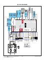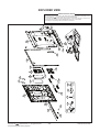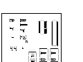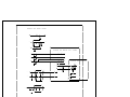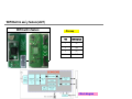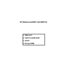
1
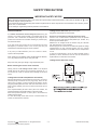
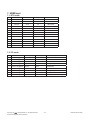
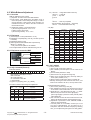
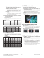
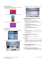
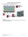
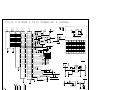
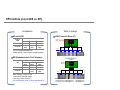
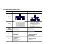
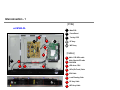
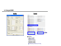
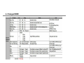
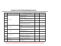
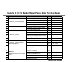
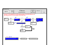
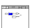
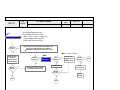
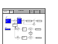
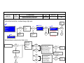
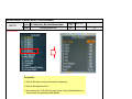
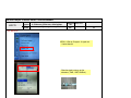
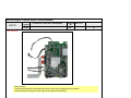
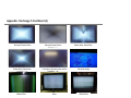
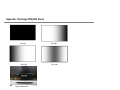
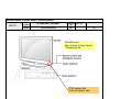
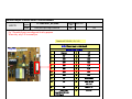
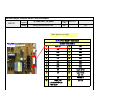
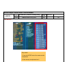
Internal Use Only North/Latin America Europe/Africa Asia/Oceania http://aic.lgservice.com http://eic.lgservice.com http://biz.lgservice.com LED LCD TV SERVICE MANUAL CHASSIS : LD22E MODEL: 32LM660S/660T/669S/669T MODEL: 32LM660S/660T-ZA 32LM669S/669T-ZC CAUTION BEFORE SERVICING THE CHASSIS, READ THE SAFETY PRECAUTIONS IN THIS MANUAL. P/NO : MFL67360905 (1204-REV00) Printed in Korea CONTENTS CONTENTS . ............................................................................................. 2 SAFETY PRECAUTIONS ......................................................................... 3 SERVICING PRECAUTIONS..................................................................... 4 SPECIFICATION........................................................................................ 6 ADJUSTMENT INSTRUCTION............................................................... 10 SCREW ASSEMBLY WORKING GUIDE ............................................... 18 BLOCK DIAGRAM................................................................................... 19 EXPLODED VIEW .................................................................................. 20 SCHEMATIC CIRCUIT DIAGRAM .............................................................. Copyright © LG Electronics. Inc. All rights reserved. Only for training and service purposes -2- LGE Internal Use Only SAFETY PRECAUTIONS IMPORTANT SAFETY NOTICE Many electrical and mechanical parts in this chassis have special safety-related characteristics. These parts are identified by in the Schematic Diagram and Exploded View. It is essential that these special safety parts should be replaced with the same components as recommended in this manual to prevent Shock, Fire, or other Hazards. Do not modify the original design without permission of manufacturer. General Guidance Leakage Current Hot Check (See below Figure) Plug the AC cord directly into the AC outlet. An isolation Transformer should always be used during the servicing of a receiver whose chassis is not isolated from the AC power line. Use a transformer of adequate power rating as this protects the technician from accidents resulting in personal injury from electrical shocks. It will also protect the receiver and it's components from being damaged by accidental shorts of the circuitry that may be inadvertently introduced during the service operation. If any fuse (or Fusible Resistor) in this TV receiver is blown, replace it with the specified. When replacing a high wattage resistor (Oxide Metal Film Resistor, over 1 W), keep the resistor 10 mm away from PCB. Keep wires away from high voltage or high temperature parts. Do not use a line Isolation Transformer during this check. Connect 1.5 K / 10 watt resistor in parallel with a 0.15 uF capacitor between a known good earth ground (Water Pipe, Conduit, etc.) and the exposed metallic parts. Measure the AC voltage across the resistor using AC voltmeter with 1000 ohms/volt or more sensitivity. Reverse plug the AC cord into the AC outlet and repeat AC voltage measurements for each exposed metallic part. Any voltage measured must not exceed 0.75 volt RMS which is corresponds to 0.5 mA. In case any measurement is out of the limits specified, there is possibility of shock hazard and the set must be checked and repaired before it is returned to the customer. Leakage Current Hot Check circuit Before returning the receiver to the customer, always perform an AC leakage current check on the exposed metallic parts of the cabinet, such as antennas, terminals, etc., to be sure the set is safe to operate without damage of electrical shock. Leakage Current Cold Check(Antenna Cold Check) With the instrument AC plug removed from AC source, connect an electrical jumper across the two AC plug prongs. Place the AC switch in the on position, connect one lead of ohm-meter to the AC plug prongs tied together and touch other ohm-meter lead in turn to each exposed metallic parts such as antenna terminals, phone jacks, etc. If the exposed metallic part has a return path to the chassis, the measured resistance should be between 1 MΩ and 5.2 MΩ. When the exposed metal has no return path to the chassis the reading must be infinite. An other abnormality exists that must be corrected before the receiver is returned to the customer. Copyright © LG Electronics. Inc. All rights reserved. Only for training and service purposes -3- LGE Internal Use Only SERVICING PRECAUTIONS CAUTION: Before servicing receivers covered by this service manual and its supplements and addenda, read and follow the SAFETY PRECAUTIONS on page 3 of this publication. NOTE: If unforeseen circumstances create conflict between the following servicing precautions and any of the safety precautions on page 3 of this publication, always follow the safety precautions. Remember: Safety First. General Servicing Precautions 1. Always unplug the receiver AC power cord from the AC power source before; a. Removing or reinstalling any component, circuit board module or any other receiver assembly. b. Disconnecting or reconnecting any receiver electrical plug or other electrical connection. c. Connecting a test substitute in parallel with an electrolytic capacitor in the receiver. CAUTION: A wrong part substitution or incorrect polarity installation of electrolytic capacitors may result in an explosion hazard. 2. Test high voltage only by measuring it with an appropriate high voltage meter or other voltage measuring device (DVM, FETVOM, etc) equipped with a suitable high voltage probe. Do not test high voltage by "drawing an arc". 3. Do not spray chemicals on or near this receiver or any of its assemblies. 4. Unless specified otherwise in this service manual, clean electrical contacts only by applying the following mixture to the contacts with a pipe cleaner, cotton-tipped stick or comparable non-abrasive applicator; 10 % (by volume) Acetone and 90 % (by volume) isopropyl alcohol (90 % - 99 % strength) CAUTION: This is a flammable mixture. Unless specified otherwise in this service manual, lubrication of contacts in not required. 5. Do not defeat any plug/socket B+ voltage interlocks with which receivers covered by this service manual might be equipped. 6. Do not apply AC power to this instrument and/or any of its electrical assemblies unless all solid-state device heat sinks are correctly installed. 7. Always connect the test receiver ground lead to the receiver chassis ground before connecting the test receiver positive lead. Always remove the test receiver ground lead last. 8. Use with this receiver only the test fixtures specified in this service manual. CAUTION: Do not connect the test fixture ground strap to any heat sink in this receiver. Electrostatically Sensitive (ES) Devices Some semiconductor (solid-state) devices can be damaged easily by static electricity. Such components commonly are called Electrostatically Sensitive (ES) Devices. Examples of typical ES devices are integrated circuits and some field-effect transistors and semiconductor “chip” components. The following techniques should be used to help reduce the incidence of component damage caused by static by static electricity. 1. Immediately before handling any semiconductor component or semiconductor-equipped assembly, drain off any electrostatic charge on your body by touching a known earth ground. Alternatively, obtain and wear a commercially available discharging wrist strap device, which should be removed to prevent potential shock reasons prior to applying power to the unit under test. Copyright © LG Electronics. Inc. All rights reserved. Only for training and service purposes 2. After removing an electrical assembly equipped with ES devices, place the assembly on a conductive surface such as aluminum foil, to prevent electrostatic charge buildup or exposure of the assembly. 3. Use only a grounded-tip soldering iron to solder or unsolder ES devices. 4. Use only an anti-static type solder removal device. Some solder removal devices not classified as “anti-static” can generate electrical charges sufficient to damage ES devices. 5. Do not use freon-propelled chemicals. These can generate electrical charges sufficient to damage ES devices. 6. Do not remove a replacement ES device from its protective package until immediately before you are ready to install it. (Most replacement ES devices are packaged with leads electrically shorted together by conductive foam, aluminum foil or comparable conductive material). 7. Immediately before removing the protective material from the leads of a replacement ES device, touch the protective material to the chassis or circuit assembly into which the device will be installed. CAUTION: Be sure no power is applied to the chassis or circuit, and observe all other safety precautions. 8. Minimize bodily motions when handling unpackaged replacement ES devices. (Otherwise harmless motion such as the brushing together of your clothes fabric or the lifting of your foot from a carpeted floor can generate static electricity sufficient to damage an ES device.) General Soldering Guidelines 1. Use a grounded-tip, low-wattage soldering iron and appropriate tip size and shape that will maintain tip temperature within the range or 500 °F to 600 °F. 2. Use an appropriate gauge of RMA resin-core solder composed of 60 parts tin/40 parts lead. 3. Keep the soldering iron tip clean and well tinned. 4. Thoroughly clean the surfaces to be soldered. Use a mall wirebristle (0.5 inch, or 1.25 cm) brush with a metal handle. Do not use freon-propelled spray-on cleaners. 5. Use the following unsoldering technique a. Allow the soldering iron tip to reach normal temperature. (500 °F to 600 °F) b. Heat the component lead until the solder melts. c. Quickly draw the melted solder with an anti-static, suctiontype solder removal device or with solder braid. CAUTION: Work quickly to avoid overheating the circuit board printed foil. 6. Use the following soldering technique. a. Allow the soldering iron tip to reach a normal temperature (500 °F to 600 °F) b. First, hold the soldering iron tip and solder the strand against the component lead until the solder melts. c. Quickly move the soldering iron tip to the junction of the component lead and the printed circuit foil, and hold it there only until the solder flows onto and around both the component lead and the foil. CAUTION: Work quickly to avoid overheating the circuit board printed foil. d. Closely inspect the solder area and remove any excess or splashed solder with a small wire-bristle brush. -4- LGE Internal Use Only IC Remove/Replacement Some chassis circuit boards have slotted holes (oblong) through which the IC leads are inserted and then bent flat against the circuit foil. When holes are the slotted type, the following technique should be used to remove and replace the IC. When working with boards using the familiar round hole, use the standard technique as outlined in paragraphs 5 and 6 above. 3. Solder the connections. CAUTION: Maintain original spacing between the replaced component and adjacent components and the circuit board to prevent excessive component temperatures. Circuit Board Foil Repair Excessive heat applied to the copper foil of any printed circuit board will weaken the adhesive that bonds the foil to the circuit board causing the foil to separate from or "lift-off" the board. The following guidelines and procedures should be followed whenever this condition is encountered. Removal 1. Desolder and straighten each IC lead in one operation by gently prying up on the lead with the soldering iron tip as the solder melts. 2. Draw away the melted solder with an anti-static suction-type solder removal device (or with solder braid) before removing the IC. Replacement 1. Carefully insert the replacement IC in the circuit board. 2. Carefully bend each IC lead against the circuit foil pad and solder it. 3. Clean the soldered areas with a small wire-bristle brush. (It is not necessary to reapply acrylic coating to the areas). At IC Connections To repair a defective copper pattern at IC connections use the following procedure to install a jumper wire on the copper pattern side of the circuit board. (Use this technique only on IC connections). "Small-Signal" Discrete Transistor Removal/Replacement 1. Remove the defective transistor by clipping its leads as close as possible to the component body. 2. Bend into a "U" shape the end of each of three leads remaining on the circuit board. 3. Bend into a "U" shape the replacement transistor leads. 4. Connect the replacement transistor leads to the corresponding leads extending from the circuit board and crimp the "U" with long nose pliers to insure metal to metal contact then solder each connection. Power Output, Transistor Device Removal/Replacement 1. Heat and remove all solder from around the transistor leads. 2. Remove the heat sink mounting screw (if so equipped). 3. Carefully remove the transistor from the heat sink of the circuit board. 4. Insert new transistor in the circuit board. 5. Solder each transistor lead, and clip off excess lead. 6. Replace heat sink. Diode Removal/Replacement 1. Remove defective diode by clipping its leads as close as possible to diode body. 2. Bend the two remaining leads perpendicular y to the circuit board. 3. Observing diode polarity, wrap each lead of the new diode around the corresponding lead on the circuit board. 4. Securely crimp each connection and solder it. 5. Inspect (on the circuit board copper side) the solder joints of the two "original" leads. If they are not shiny, reheat them and if necessary, apply additional solder. 1. Carefully remove the damaged copper pattern with a sharp knife. (Remove only as much copper as absolutely necessary). 2. carefully scratch away the solder resist and acrylic coating (if used) from the end of the remaining copper pattern. 3. Bend a small "U" in one end of a small gauge jumper wire and carefully crimp it around the IC pin. Solder the IC connection. 4. Route the jumper wire along the path of the out-away copper pattern and let it overlap the previously scraped end of the good copper pattern. Solder the overlapped area and clip off any excess jumper wire. At Other Connections Use the following technique to repair the defective copper pattern at connections other than IC Pins. This technique involves the installation of a jumper wire on the component side of the circuit board. 1. Remove the defective copper pattern with a sharp knife. Remove at least 1/4 inch of copper, to ensure that a hazardous condition will not exist if the jumper wire opens. 2. Trace along the copper pattern from both sides of the pattern break and locate the nearest component that is directly connected to the affected copper pattern. 3. Connect insulated 20-gauge jumper wire from the lead of the nearest component on one side of the pattern break to the lead of the nearest component on the other side. Carefully crimp and solder the connections. CAUTION: Be sure the insulated jumper wire is dressed so the it does not touch components or sharp edges. Fuse and Conventional Resistor Removal/Replacement 1. Clip each fuse or resistor lead at top of the circuit board hollow stake. 2. Securely crimp the leads of replacement component around notch at stake top. Copyright © LG Electronics. Inc. All rights reserved. Only for training and service purposes -5- LGE Internal Use Only SPECIFICATION NOTE : Specifications and others are subject to change without notice for improvement. 1. Application range This specification is applied to the LCD TV used LD22E chassis. 3. Test method 2. Requirement for Test Each part is tested as below without special appointment. 1) Performance: LGE TV test method followed 2) Demanded other specification - Safety : CE, IEC specification - EMC : CE, IEC - Wireless : Wireless HD Specification (Option) 1) Temperature: 25 °C ± 5 °C(77 °F ± 9 °F), CST: 40 °C ± 5 °C 2) Relative Humidity: 65 % ± 10 % 3) Power Voltage : Standard input voltage (AC 100-240 V~, 50/60 Hz) * Standard Voltage of each products is marked by models. 4) Specification and performance of each parts are followed each drawing and specification by part number in accordance with BOM. 5) The receiver must be operated for about 20 minutes prior to the adjustment. 4. Model General Specification No. Item Specification Remarks DTV & Analog (Total 37 countries) DTV (MPEG2/4, DVB-T) : 30 countries Germany, Netherland, Switzerland, Hungary, Austria, Slovenia, Bulgaria, France, Spain, Italy, Belgium, Russia, Luxemburg, Greece, Czech, Croatia, Turkey, Moroco, Ireland, Latvia, Estonia, Lithuania, Poland, Portugal, Romania, Albania, Bosnia, Serbia, Slovakia, Beralus DTV (MPEG2/4, DVB-T2) : 7 countries UK, Sweden, Denmark, Finland, Norway, Ukraine, Kazakhstan, Ireland 1 Market DTV (MPEG2/4, DVB-C) : 37 countries Germany, Netherland, Switzerland, Hungary, Austria, Slovenia, Bulgaria, France, Spain, Italy, Belgium, Russia, Luxemburg, Greece, Czech, Croatia, Turkey, Moroco, Ireland, Latvia, Estonia, Lithuania, Poland, Portugal, Romania, Albania, Bosnia, Serbia, Slovakia, Beralus, UK, Sweden, Denmark, Finland, Norway, Ukraine, Kazakhstan EU(PAL Market-36Countries) DTV (MPEG2/4,DVB-S) : 30 countries Germany, Netherland, Switzerland, Hungary, Austria, Slovenia, Bulgaria, France, Spain, Italy, Belgium, Russia, Luxemburg, Greece, Czech, Croatia, Turkey, Moroco, Ireland, Latvia, Estonia, Lithuania, Poland, Portugal, Romania, Albania, Bosnia, Serbia, Slovakia, Beralus Supported satellite : 22 satellites HISPASAT 1C/1D, ATLANTIC BIRD 2, NILESAT 101/102, ATLANTIC BIRD 3, AMOS 2/3, THOR 5/6, IRIUS 4, EUTELSAT-W3A, EUROBIRD 9°, EUTELSAT-W2A, HOTBIRD 6/8/9, EUTELSAT-SESAT, ASTRA 1L/H/M/KR, ASTRA 3°/3B, BADR 4/6, ASTRA 2D, EUROBIRD 3, EUTELSATW7, HELLASSAT 2, EXPRESS AM1, TURKSAT 2°/3°, INTERSAT10 Copyright © LG Electronics. Inc. All rights reserved. Only for training and service purposes -6- LGE Internal Use Only No. 2 Item Broadcasting system Specification Remarks 1) PAL-BG 2) PAL-DK 3) PAL-I/I’ 4) SECAM L/L’, DK, BG, I 5) DVB-T 6) DVB-C 7) DVB-T2 8) DVB-S DVB-S: Satellite ► DVB-T - Guard Interval(Bitrate_Mbit/s) 1/4, 1/8, 1/16, 1/32 - Modulation : Code Rate QPSK : 1/2, 2/3, 3/4, 5/6, 7/8 16-QAM : 1/2, 2/3, 3/4, 5/6, 7/8 64-QAM : 1/2, 2/3, 3/4, 5/6, 7/8 3 Receiving system ► DVB-T2 - Guard Interval(Bitrate_Mbit/s) 1/4, 1/8, 1/16, 1/32, 1/128, 19/128, 19/256, - Modulation : Code Rate QPSK : 1/2, 2/5, 2/3, 3/4, 5/6 16-QAM : 1/2, 2/5, 2/3, 3/4, 5/6 64-QAM : 1/2, 2/5, 2/3, 3/4, 5/6 256-QAM : 1/2, 2/5, 2/3, 3/4, 5/6 Analog : Upper Heterodyne Digital : COFDM, QAM ► DVB-C - Symbolrate : 4.0Msymbols/s to 7.2Msymbols/s - Modulation : 16QAM, 64-QAM, 128-QAM and 256-QAM ► DVB-S/S2 - symbolrate DVB-S2 (8PSK / QPSK) : 2 ~ 45Msymbol/s DVB-S (QPSK) : 2 ~ 45Msymbol/s - viterbi DVB-S mode : 1/2, 2/3, 3/4, 5/6, 7/8 DVB-S2 mode : 1/2, 2/3, 3/4, 3/5, 4/5, 5/6, 8/9, 9/10 4 Scart Gender Jack (1EA) PAL, SECAM 5 Video Input RCA(1EA) PAL, SECAM, NTSC 6 Head phone out 7 Component Input (1EA) 8 RGB Input 9 HDMI Input (4EA) 10 Audio Input (3EA) 11 12 13 SPDIF out (1EA) USB (3EA) Ethernet Connect(1EA) Scart jack is Full scart and support MNT/DTV-OUT (not support DTV Auto AV) 4 System : PAL, SECAM, NTSC, PAL60 AV gender jack 1EA Antenna, AV1, AV2, Component, RGB, HDMI1, HDMI2, HDMI3, HDMI4, USB1, USB2, USB3 Y/Cb/Cr Y/Pb/Pr RGB-PC HDMI1-DTV HDMI2-DTV HDMI3-DTV HDMI4-DTV RGB/DVI Audio Component AV SPDIF out EMF, DivX HD, For SVC (download) Ethernet Connect Copyright © LG Electronics. Inc. All rights reserved. Only for training and service purposes -7- Component Gender 1EA Analog(D-SUB 15PIN) HDMI4 : PC support(HDMI version 1.3) Support HDCP L/R Input JPEG, MP3, DivX HD LGE Internal Use Only 5. Component Video Input (Y, Cb/Pb, Cr/Pr) No. Resolution H-freq(kHz) V-freq(Hz) Porposed 1 720×480 15.73 60.00 SDTV, DVD 480i 2 720×480 15.63 59.94 SDTV, DVD 480i 3 720×480 31.47 59.94 480p 4 720×480 31.50 60.00 480p 5 720×576 15.625 50.00 SDTV, DVD 625 Line 6 720×576 31.25 50.00 HDTV 576p 7 1280×720 45.00 50.00 HDTV 720p 8 1280×720 44.96 59.94 HDTV 720p 9 1280×720 45.00 60.00 HDTV 720p 10 1920×1080 31.25 50.00 HDTV 1080i 11 1920×1080 33.75 60.00 HDTV 1080i 12 1920×1080 33.72 59.94 HDTV 1080i 13 1920×1080 56.250 50 HDTV 1080p 14 1920×1080 67.5 60 HDTV 1080p 6. RGB input (PC) No. Resolution H-freq(kHz) V-freq.(Hz) Proposed 1 640 x 350 @70Hz 31.468 70.09 EGA 2 720 x 400 @70Hz 31.469 70.08 DOS 3 640 x 480 @60Hz 31.469 59.94 VESA(VGA) 4 800 x 600 @60Hz 37.879 60.31 VESA(SVGA) 5 1024 x 768 @60Hz 48.363 60.00 VESA(XGA) 6 1152 x 864 @60Hz 54.348 60.053 VESA 7 1360 x 768 @60Hz 47.712 60.015 VESA(WXGA) 8 1920 x 1080 @60Hz 67.5 60.00 WUXGA(Reduced Blanking)) Copyright © LG Electronics. Inc. All rights reserved. Only for training and service purposes -8- LGE Internal Use Only 7. HDMI Input 7.1. DTV mode No. Resolution H-freq(kHz) V-freq.(kHz) Proposed 1. 640*480 2. 720*480 31.469 / 31.5 59.94/60 SDTV 480P 31.469 / 31.5 59.94 / 60 SDTV 480P 3. 4. 720*576 31.25 50 SDTV 576P 720*576 15.625 50 SDTV 576I 5. 1280*720 37.500 50 HDTV 720P 6. 1280*720 44.96 / 45 59.94 / 60 HDTV 720P 7. 1920*1080 33.72 / 33.75 59.94 / 60 HDTV 1080I 8. 1920*1080 28.125 50.00 HDTV 1080I 9. 1920*1080 26.97 / 27 23.97 / 24 HDTV 1080P 10. 1920*1080 25 HDTV 1080P 11. 1920*1080 33.716 / 33.75 29.976 / 30.00 HDTV 1080P 12. 1920*1080 56.250 50 HDTV 1080P 13. 1920*1080 67.43 / 67.5 59.94 / 60 HDTV 1080P 7.2. PC mode No. Resolution 1 640 x 350 @70Hz 31.468 H-freq(kHz) 70.09 V-freq.(Hz) EGA 2 720 x 400 @70Hz 31.469 70.08 DOS 3 640 x 480 @60Hz 31.469 59.94 VESA(VGA) 4 800 x 600 @60Hz 37.879 60.31 VESA(SVGA) 5 1024 x 768 @60Hz 48.363 60.00 VESA(XGA) 6 1152 x 864 @60Hz 54.348 60.053 VESA 7 1280 x 1024 @60Hz 63.981 60.020 VESA(SXGA) 8 1360 x 768 @60Hz 47.712 60.015 VESA(WXGA) 9 1920 x 1080 @60Hz 67.5 60.00 WUXGA(Reduced Blanking)) Copyright © LG Electronics. Inc. All rights reserved. Only for training and service purposes -9- Proposed LGE Internal Use Only ADJUSTMENT INSTRUCTION 1. Application Range 3.1.3. Adjustment This specification sheet is applied to all of the LED LCD TV with LD22E chassis. 2. Designation (1) Because this is not a hot chassis, it is not necessary to use an isolation transformer. However, the use of isolation transformer will help protect test instrument. (2) Adjustment must be done in the correct order. (3) The adjustment must be performed in the circumstance of 25 °C ± 5 °C of temperature and 65 % ± 10 % of relative humidity if there is no specific designation. (4) The input voltage of the receiver must keep AC 100-240 V~, 50/60 Hz. (5) The receiver must be operated for about 5 minutes prior to the adjustment when module is in the circumstance of over 15. In case of keeping module is in the circumstance of 0 °C, it should be placed in the circumstance of above 15 °C for 2 hours. In case of keeping module is in the circumstance of below -20 °C, it should be placed in the circumstance of above 15 °C for 3 hours. [Caution] When still image is displayed for a period of 20 minutes or longer (Especially where W/B scale is strong. Digital pattern 13ch and/or Cross hatch pattern 09ch), there can some afterimage in the black level area. (1) Adjustment method ▪ Don’t need to adjust ADC because there is data in OTP and adjusted initially. ▪ Check ADC adjustment 1) Press In start key on the Adj. Remote Control, then Adjust ADC(OTP) status is displayed on “1.Adjustment check”. Select “2.ADC Data”, then ADC data is displayed. 2) Press Adj. key on the Adjustmetn Remote Control, and select “9.ADC Calibration”. Set up the ADC Type to OTP, then Select [Start] button by pressing Enter key, Component and RGB are Writed and display Success or NG. (2) Adj. protocol Protocol Enter adj. mode Source change Begin adj. Command a 00 OK00x xb 00 04 b 00 OK04x (Adjust 480i, 1080p Comp1 ) xb 00 06 b 00 OK06x (Adjust 1920*1080 RGB) ad 00 10 OKx (Case of Success) NGx (Case of Fail) Return adj. result Read adj. data Set ACK aa 00 00 (main) ad 00 20 (main) 000000000000000000000000007c007b006dx (sub ) (Sub) 000000070000000000000000007c00830077x ad 00 21 Confirm adj. ad 00 99 NG 03 00x (Fail) NG 03 01x (Fail) NG 03 02x (Fail) OK 03 03x (Success) End adj. aa 00 90 a 00 OK90x Ref.) ADC Adj. RS232C Protocol_Ver1.0 3. Automatic Adjustment 3.1. ADC Adjustment 3.1.1. Overview ADC adjustment is needed to find the optimum black level and gain in Analog-to-Digital device and to compensate RGB deviation. 3.1.2. Equipment & Condition (3) Adj. order - aa 00 00 [Enter ADC adj. mode] - xb 00 04 [Change input source to Component1 (480i& 1080p)] - ad 00 10 [Adjust 480i&1080p Comp1] - xb 00 06 [Change input source to RGB(1024*768)] - ad 00 10 [Adjust 1920*1080 RGB] - ad 00 90 End adj. (1) USB to RS-232C Jig (2) M SPG-925 Series Pattern Generator(MSPG-925FA, pattern - 65) - Resolution :1080P Comp1 1920*1080 RGB - Pattern : Horizontal 100% Color Bar Pattern - Pattern level : 0.7 ± 0.1 Vp-p - Image Copyright © LG Electronics. Inc. All rights reserved. Only for training and service purposes - 10 - LGE Internal Use Only 3.2. M AC address D/L, CI+ key D/L, Widevine key D/L, ESN D/L 3.3.3. WIDEVINE key Inspection - Confirm key input data at the "IN START" MENU Mode. Connect: USB port Communication Prot connection ▪ Com 1,2,3,4 and 115200(Baudrate) Mode check: Online Only ▪ Check the test process: DETECT -> MAC -> CI -> Widevine -> ESN ▪. Play: START ▪. Result: Ready, Test, OK or NG ▪. Printer Out (MAC Address Label) G 3.4. LAN PORT INSPECTION(PING TEST) Connect SET → LAN port == PC → LAN Port SET PC 3.4.1. Equipment setting (1) Play the LAN Port Test PROGRAM. (2) Input IP set up for an inspection to Test Program. *IP Number : 12.12.2.2 Play: Start 3.4.2. LAN PORT inspection(PING TEST) 3.3. LAN (1) Play the LAN Port Test Program. (2) Connect each other LAN Port Jack. (3) Play Test (F9) button and confirm OK Message. (4) Remove LAN cable. 3.3.1. Equipment & Condition ▪ Each other connection to LAN Port of IP Hub and Jig 3.3.2. LAN inspection solution ▪ LAN Port connection with PCB ▪ Network setting at MENU Mode of TV ▪ Setting automatic IP ▪ Setting state confirmation → If automatic setting is finished, you confirm IP and MAC Address. Copyright © LG Electronics. Inc. All rights reserved. Only for training and service purposes - 11 - LGE Internal Use Only 3.5. Model name & Serial number Download 2) Check the key download for transmitted command (RS232: ci 00 10) 3.5.1. Model name & Serial number D/L Press "Power on" key of service remote control. (Baud rate : 115200 bps) ▪ Connect RS232 Signal Cable to RS-232 Jack. ▪ Write Serial number by use RS-232. ▪ Must check the serial number at Instart menu. ▪ CMD 1 CMD 2 C I Data 0 1 0 3) Result value - Normally status for download : OKx - Abnormally status for download : NGx 3.5.2. Method & notice (1) Serial number D/L is using of scan equipment. (2) Setting of scan equipment operated by Manufacturing Technology Group. (3) Serial number D/L must be conformed when it is produced in production line, because serial number D/L is mandatory by D-book 4.0 3.6.2. Check the method of CI+ key value(RS232) 1) Into the main ass’y mode(RS232: aa 00 00) CMD 1 CMD 2 A A Data 0 0 0 2) Check the mothed of CI+ key by command (RS232: ci 00 20) * Manual Download (Model Name and Serial Number) If the TV set is downloaded by OTA or service man, sometimes model name or serial number is initialized.(Not always) It is impossible to download by bar code scan, so It need Manual download. 1) Press the "Instart" key of Adjustment remote control. 2) Go to the menu "5.Model Number D/L" like below photo. 3) Input the Factory model name(ex 47LM760S-ZB-A) or Serial number like photo. CMD 1 CMD 2 C I Data 0 2 0 3) Result value i 01 OK 1d1852d21c1ed5dcx CI+ Key Value 3.7. WIFI MAC ADDRESS CHECK (1) Using RS232 Transmission H-freq(kHz) V-freq.(Hz) [A][I][][Set ID][][20][Cr] [O][K][X] or [NG] (2) Check the menu on in-start. 4) Check the model name Instart menu. → Factory name displayed. (ex 47LM760S-ZB) 5) C heck the Diagnostics.(DTV country only) → Buyer model displayed. (ex 47LM760S-ZB) 3.6. CI+ Key checking method - Check the Section 3.2 Check whether the key was downloaded or not at ‘In Start’ menu. (Refer to below). => Check the Download to CI+ Key value in LGset. 3.6.1. Check the method of CI+ Key value (1) Check the method on Instart menu (2) Check the method of RS232C Command 1) Into the main ass’y mode(RS232: aa 00 00) CMD 1 CMD 2 A A Data 0 0 0 Copyright © LG Electronics. Inc. All rights reserved. Only for training and service purposes - 12 - LGE Internal Use Only 4. Manual Adjustment ▪ Reference - HDMI1 ~ HDMI4 / RGB - In the data of EDID, bellows may be different by S/W or Input mode. ⓐ. Product ID HEX EDID Table DDC Function * ADC adjustment is not needed because of OTP(Auto ADC adjustment) 4.1 EDID(The Extended Display Identification Data)/DDC(Display Data Channel) download 0001 4.1.1. Overview It is a VESA regulation. A PC or a MNT will display an optimal resolution through information sharing without any necessity of user input. It is a realization of "Plug and Play". 4.1.2. Equipment Chassis - Since embedded EDID data is used, EDID download JIG, HDMI cable and D-sub cable are not need. - Adjustment remote control For HDMI EDID DVI-D to HDMI or HDMI to HDMI 00 00 00 FC 00 4C 47 20 54 56 0A 20 20 20 20 20 20 20 ⓔ. Checksum: Changeable by total EDID data. ⓔ1 (1) Press "ADJ" key on the Adjustment remote control then select "10.EDID D/L", By pressing "Enter" key, enter EDID D/L menu. (2) S elect "Start" button by pressing "Enter" key, HDMI1/ HDMI2/ HDMI3/ HDMI4/ RGB are writing and display OK or NG. For Analog Analog/Digital MODEL NAME(HEX) LD22E 4.1.3. Download method D-sub to D-sub 01 00 ⓑ. Serial No: Controlled on production line. ⓒ. Month, Year: Controlled on production line: ex) Week : '01' -> '01' Year : '2012' -> '16' fix ⓓ. Model Name(Hex): LGTV ⓔ2 10 bit/ Xvycc ⓔ2 8 bit/ Xvycc ⓔ2 10 bit/ none XvYcc ⓔ2 8 bit/ none XvYcc ⓔ3 HDMI1 43 11 49 15 4D X HDMI2 43 01 39 05 3D X HDMI3 43 F1 29 F5 2D X HDMI4 43 E1 19 E5 1D X RGB X X X X X 5C ⓕ. Vendor Specific(HDMI) 1) Deep color (module 10bit) INPUT MODEL NAME(HEX) HDMI1 78 03 0C 00 10 00 B8 2D 20 C0 0E 01 4F 3F FC 08 10 18 10 06 10 16 10 28 10 HDMI2 78 03 0C 00 20 00 B8 2D 20 C0 0E 01 4F 3F FC 08 10 18 10 06 10 16 10 28 10 HDMI3 78 03 0C 00 30 00 B8 2D 20 C0 0E 01 4F 3F FC 08 10 18 10 06 10 16 10 28 10 HDMI4 78 03 0C 00 40 00 B8 2D 20 C0 0E 01 4F 3F FC 08 10 18 10 06 10 16 10 28 10 4.1.4. EDID DATA (1) 3D EDID DATA 2) None deep color (module 8bit) INPUT MODEL NAME(HEX) HDMI1 78 03 0C 00 10 00 80 2D 20 C0 0E 01 4F 3F FC 08 10 18 10 06 10 16 10 28 10 HDMI2 78 03 0C 00 20 00 80 2D 20 C0 0E 01 4F 3F FC 08 10 18 10 06 10 16 10 28 10 HDMI3 78 03 0C 00 30 00 80 2D 20 C0 0E 01 4F 3F FC 08 10 18 10 06 10 16 10 28 10 HDMI4 78 03 0C 00 40 00 80 2D 20 C0 0E 01 4F 3F FC 08 10 18 10 06 10 16 10 28 10 ⓖ Colorimetry Data Block(HDMI) - The Model not supporting XvYcc(Except for LM7600) INPUT HDMI1 HDMI2 HDMI3 HDMI4 Copyright © LG Electronics. Inc. All rights reserved. Only for training and service purposes - 13 - MODEL NAME(HEX) E3 05 00 00 E3 05 00 00 E3 05 00 00 E3 05 00 00 LGE Internal Use Only 4.2. White Balance Adjustment Ex) wb 00 00 -> Begin white balance auto-adj. wb 00 10 -> Gain adj. ja 00 ff -> Adj. data jb 00 c0 ... ... wb 00 1f → Gain adj. completed *(wb 00 20(Start), wb 00 2f(end)) → Off-set adj. wb 00 ff → End white balance auto-adj. 4.2.1. Overview ▪ W/B adj. Objective & How-it-works (1) Objective: To reduce each Panel's W/B deviation (2) How-it-works : When R/G/B gain in the OSD is at 192, it means the panel is at its Full Dynamic Range. In order to prevent saturation of Full Dynamic range and data, one of R/G/B is fixed at 192, and the other two is lowered to find the desired value. (3) Adjustment condition : normal temperature 1) Surrounding Temperature : 25 °C ± 5 °C 2) Warm-up time: About 5 Min 3) Surrounding Humidity : 20 % ~ 80 % ▪ Adj. Map Adj. item 4.2.2. Equipment (1) Color Analyzer: CA-210 (LED Module : CH 14) (2) Adjustment Computer(During auto adj., RS-232C protocol is needed) (3) Adjustment Remote control (4) Video Signal Generator MSPG-925F 720p/204-Gray (Model: 217, Pattern: 49) -> Only when internal pattern is not available ▪ Color Analyzer Matrix should be calibrated using CS-100. Cool Command (lower caseASCII) Data Range (Hex.) CMD1 MIN MAX R Gain j g CMD2 00 C0 G Gain j h 00 C0 B Gain j i 00 C0 R Gain j a 00 C0 G Gain j b 00 C0 B Gain j c 00 C0 R Gain j d 00 C0 G Gain j e 00 C0 B Gain j f 00 C0 Default (Decimal) R Cut G Cut B Cut Medium 4.2.3. Equipment connection MAP R Cut G Cut B Cut Co lo r Analyzer RS -232C Probe Warm Co m p ut er RS -232C R Cut RS -232C G Cut Pat t ern Generat o r Signal Source * If TV internal pattern is used, not needed 4.2.5. Adj. method 4.2.4. Adj. Command (Protocol) <Command Format> START 6E A 50 A LEN A 03 A CMD A 00 A VAL A CS STOP - LEN: Number of Data Byte to be sent - CMD: Command - VAL: FOS Data value - CS: Checksum of sent data - A: Acknowledge Ex) [Send: JA_00_DD] / [Ack: A_00_okDDX] ▪ RS-232C Command used during auto-adjustment. RS-232C COMMAND [CMD ID DATA] (2) Manual adjustment. method 1) Set TV in Adj. mode using P-Only key. 2) Zero Calibrate the probe of Color Analyzer, then place it on the center of LCD module within 10 cm of the surface. 3) Press ADJ key → EZ adjust using adj. R/C → 7. WhiteBalance then press the cursor to the right(key ►). (When right key(►) is pressed 216 Gray internal pattern will be displayed) 4) One of R Gain / G Gain / B Gain should be fixed at 192, and the rest will be lowered to meet the desired value. 5) Adjustment is performed in COOL, MEDIUM, WARM 3 modes of color temperature. ▪ If internal pattern is not available, use RF input. In EZ Adj. menu 7.White Balance, you can select one of 2 Test-pattern: ON, OFF. Default is inner(ON). By selecting OFF, you can adjust using RF signal in 216 Gray pattern. Explantion wb 00 00 Begin White Balance adjustment wb 00 10 Gain adjustment(internal white pattern) wb 00 1f Gain adjustment completed wb 00 20 Offset adjustment(internal white pattern) wb 00 2f Offset adjustment completed wb 00 ff End White Balance adjustment (internal pattern disappears ) Copyright © LG Electronics. Inc. All rights reserved. Only for training and service purposes (1) Auto adj. method 1) Set TV in adj. mode using P-Only key. 2) Zero calibrate probe then place it on the center of the Display. 3) Connect Cable.(RS-232C to USB) 4) Select mode in adj. Program and begin adj. 5) When adj. is complete (OK Sign), check adj. status pre mode. (Warm, Medium, Cool) 6) Remove probe and RS-232C cable to complete adj. ▪ W/B Adj. must begin as start command “wb 00 00” , and finish as end command “wb 00 ff”, and Adj. offset if need. - 14 - LGE Internal Use Only ▪ Adjustment condition and cautionary items 1) Lighting condition in surrounding area Surrounding lighting should be lower 10 lux. Try to isolate adj. area into dark surrounding. 2) Probe location : Color Analyzer(CA-210) probe should be within 10 cm and perpendicular of the module surface.(80° ~ 100°) 3) Aging time - After Aging Start, Keep the Power ON status during 5 Minutes. - In case of LCD, Back-light on should be checked using no signal or Full-white pattern. 4.3. EYE-Q function check (1) Turn on TV. (2) Press EYE key of Adjustment remote control. (3) Cover the Eye Q II sensor on the front of the using your hand and wait for 6 seconds. (4) Confirm that R/G/B value is lower than 10 of the "Raw Data (Sensor data, Back light)". If after 6 seconds, R/G/B value is not lower than 10, replace Eye Q II sensor. (5) Remove your hand from the Eye Q II sensor and wait for 6 seconds. (6) Confirm that "ok" pop up. If change is not seen, replace Eye Q II sensor. 4.2.6. Reference(White balance adjusmtment coordinate and color temperature) ▪ Luminance : 204 Gray ▪ Standard color coordinate and temperature using CS-1000 (over 26 inch) Coordinate Mode x y Temp ∆uv Cool 0.269 0.273 13000 K 0.0000 Medium 0.285 0.293 9300 K 0.0000 Warm 0.313 0.329 6500 K 0.0000 4.4. Local Dimming Function Check Step 1) Turn on TV. Step 2) Press “TILT” key on the Adj. R/C. Step 3) At the Local Dimming mode, module Edge Backlight moving right to left Back light of IOP module moving. Step 4) Confirm the Local Dimming mode. Step 5) Press "exit" key. ▪ Standard color coordinate and temperature using CA-210(CH 14) Coordinate Mode Temp ∆uv x y Cool 0.269 ± 0.002 0.273 ± 0.002 13000 K 0.0000 Medium 0.285 ± 0.002 0.293 ± 0.002 9300 K 0.0000 Warm 0.313 ± 0.002 0.329 ± 0.002 6500 K 0.0000 4.2.7. LED White balance table - EDGE LED module change color coordinate because of aging time. - Apply under the color coordinate table, for compensated aging time. - LM76/67/66 series GP4 Aging time (Min) 1 2 3 4 5 6 7 8 9 0-2 3-5 6-9 10-19 20-35 36-49 50-79 80-119 Over 120 Cool X 269 283 282 281 279 277 274 271 270 269 y 273 293 291 290 289 284 279 277 274 273 Medium x y 285 293 299 313 298 311 297 310 295 309 293 304 290 299 287 297 286 294 285 293 Local Dimming Demo (Edge LED Model) 4.5. Magic Motion Remote control test Warm x 313 320 319 318 316 314 311 308 307 306 Copyright © LG Electronics. Inc. All rights reserved. Only for training and service purposes y 329 339 337 336 335 330 325 323 320 319 - 15 - (1) Equipment : RF Remote control for test, IR-KEY-Code Remote control for test (2) You must confirm the battery power of RF-Remote control before test(recommend that change the battery per every lot) (3) Sequence (test) 1) if you select the "Start(Wheel)" key on the Adjustment remote control, you can pairing with the TV SET. 2) You can check the cursor on the TV Screen, when select the "Wheel" key on the Adjustment remote control. 3) You must remove the pairing with the TV Set by select "Mute" key on the Adjustment remote control LGE Internal Use Only 4.6. 3D function test Step 4) If the system finds any AP like blow PIC, it is working well. (Pattern Generator MSHG-600, MSPG-6100[Support HDMI1.4]) * HDMI mode NO. 872 , pattern No.83 (1) Please input 3D test pattern like below. (2) When 3D OSD appear automatically, then select OK key. 4.8. LNB voltage and 22KHz tone check (only for DVB-S/S2 model) ▪ Test method (1) Set TV in Adj. mode using POWER ON. (2) Connect cable between satellite ANT and test JIG. (3) Press Yellow key(ETC+SWAP) in Adj Remote control to make LNB on. (4) Check LED light ‘ON’ at 18 V menu. (5) Check LED light ‘ON’ at 22 KHz tone menu. (6) Press Blue key(ETC+PIP INPUT) in Adj Remote control to make LNB off. (7) Check LED light ‘OFF’ at 18 V menu. (8) Check LED light ‘OFF’ at 22 KHz tone menu. (3) Don't wear a 3D Glasses, check the picture like below. 4.7. Wi-Fi Test ▪ Test result (1) After press LNB On key, ‘18 V LED’ and ‘22 KHz tone LED’ should be ON. (2) After press LNB OFF key, ‘18 V LED’ and ‘22 KHz tone LED’ should be OFF. Step 1) Turn on TV Step 2) Select Network Connection option in Network Menu. 4.9. Option selection per country 4.9.1. Overview - Option selection is only done for models in Non-EU 4.9.2. Method (1) Press ADJ key on the Adj. R/C, then select Country Group Meun (2) Depending on destination, select Country Group Code 04 or Country Group EU then on the lower Country option, select US, CA, MX. Selection is done using +, - or ►◄ key. Step 3) Select Start Connection button in Network Connection. 4.10. Tool Option selection ▪ Method : Press "ADJ" key on the Adjustment remote control, then select Tool option. 4.11. Ship-out mode check(In-stop) ▪ After final inspection, press "IN-STOP" key of the Adjustment remote control and check that the unit goes to Stand-by mode. Copyright © LG Electronics. Inc. All rights reserved. Only for training and service purposes - 16 - LGE Internal Use Only 6. USB S/W Download(Service only) 4.12. GND and Internal Pressure check 4.12.1. Method (1) Put the USB Stick to the USB socket. (2) Automatically detecting update file in USB Stick. - If your downloaded program version in USB Stick is Low, it didn't work. But your downloaded version is High, USB data is automatically detecting. (Download Version High & Power only mode, Set is automatically Download) (3) Show the message "Copying files from memory". (1) GND & Internal Pressure auto-check preparation - Check that Power cord is fully inserted to the SET. (If loose, re-insert) (2) Perform GND & Internal Pressure auto-check - Unit fully inserted Power cord, Antenna cable and A/V arrive to the auto-check process. - Connect D-terminal to AV JACK TESTER - Auto CONTROLLER(GWS103-4) ON - Perform GND TEST - If NG, Buzzer will sound to inform the operator. - If OK, changeover to I/P check automatically. (Remove CORD, A/V form AV JACK BOX.) - Perform I/P test - If NG, Buzzer will sound to inform the operator. - If OK, Good lamp will lit up and the stopper will allow the pallet to move on to next process. 4.12.2. Checkpoint ▪ TEST voltage - GND: 1.5 KV / min at 100 mA - SIGNAL: 3 KV / min at 100 mA ▪ TEST time: 1 second ▪ TEST POINT - G ND TEST = POWER CORD GND & SIGNAL CABLE METAL GND - Internal Pressure TEST = POWER CORD GND & LIVE & NEUTRAL ▪ LEAKAGE CURRENT: At 0.5 mArms 5. Audio No. Item Min Typ Max Unit 9 10 12 W 1. Audio practical max Output, L/R (Distortion=10% max Output) 8.10 10.8 Vrms 2. Speaker (8Ω Impedance) 9 10 12 W (4) Updating is starting. (5) Updating Completed, The TV will restart automatically. (6) If your TV is turned on, check your updated version and Tool option. (explain the Tool option, next stage) * If downloading version is more high than your TV have, TV can lost all channel data. In this case, you have to channel recover. if all channel data is cleared, you didn’t have a DTV/ ATV test on production line. Remark EQ Off AVL Off Clear Voice Off * After downloading, have to adjust Tool Option again. (1) Push "IN-START" key in service remote control. (2) Select "Tool Option 1" and push "OK" key. (3) Punch in the number. (Each model has their number) EQ Off AVL Off Clear Voice Off Measurement condition: (1) RF input: Mono, 1 KHz sine wave signal, 100 % Modulation (2) CVBS, Component: 1 KHz sine wave signal 0.5 Vrms (3) RGB PC: 1 KHz sine wave signal 0.7 Vrms Copyright © LG Electronics. Inc. All rights reserved. Only for training and service purposes - 17 - LGE Internal Use Only SCREW ASSEMBLY WORKING GUIDE ■ Screw specification and application situation A A A A חͷͲͳͤͤͤͪͥͣ͢͡ A A A A ͙;ͤ͛ͽͥͦ͑͟͝ͳͼ͑͝;ΒΔΙΚΟΖ͚ ͧ͢ חͶͲ A A A A A A A D D C C C A D D C • FAB30013202 (M3*L8, White, Taptite) • 4EA חͷͲͳͤͧͣͥ͢͢͡͡ ͙;ͥ͛ͽͥ͑͢͝ͳͼ͑͝;ΒΔΙΚΟΖ͚ ͥ חͶͲ E E חͷͲͳͤͧͣͣ͑͢͢͡͡ ͙;ͥ͛ͽͣ͑͡͝ͳͼ͑͝;ΒΔΙΚΟΖ͚ ͥ חͶͲ E E <Warning> Check Screw Type When Screw is assembled at 'A' Part. If 'C' Screw is used at the 'A' part, Module will get damaged. Copyright © LG Electronics. Inc. All rights reserved. Only for training and service purposes - 18 - LGE Internal Use Only DVB-S Air/ Cable TUNER (S2) TUNER (T/C) sui DIGITAL DEMOD (S2) DIGITAL DEMOD (T/C) ANALOG DEMOD Copyright © LG Electronics. Inc. All rights reserved. Only for training and service purposes - 19 RS-232C LAN OPTIC PC-AUDIO PC-RGB HDMI4 HDMI3 HDMI2 HDMI1 USB3 USB_WIFI USB1 USB2 IF(+/-) P_TS Rear Side P_TS CVBS P_TS jpG Ethernet (HDCP SYSTEM DDR3 X 1600 X 16 (2Gb) UART I2C IR UART SPI I2S Out EPI CONTROLER A/B DDR SYSTEM DDR3 X 1600 X 16 (2Gb) MTK EEPROM) SPDIF OUT L/R In RGB,H/V HDMI MUX USB TS_S/P CVBS T/C Demod X_TAL 27MHz Remote Control M-Remote Module LOCAL DIMMING ( STA) Audio AMP Sub Micom (RENESASA) 50P 50P eMMC X 1 (2GB) SYSTEM EEPROM X 1 (256Kb) SYSTEM DDR3 X 1600 X 16 (2Gb) SYSTEM DDR3 X 1600 X 16 (2Gb) BLOCK DIAGRAM LGE Internal Use Only EXPLODED VIEW IMPORTANT SAFETY NOTICE * Set + Stand * Stand Base + Body A21 501 A2 301 500 300 A22 A10 200 122 AG1 123 AG2 Clip Type (Option) 120 522 800 LV1 LV2 530 540 810 521 310 510 410 560 910 900 400 700 570 710 Many electrical and mechanical parts in this chassis have special safety-related characteristics. These parts are identified by in the Schematic Diagram and EXPLODED VIEW. It is essential that these special safety parts should be replaced with the same components as recommended in this manual to prevent X-RADIATION, Shock, Fire, or other Hazards. Do not modify the original design without permission of manufacturer. Copyright © LG Electronics. Inc. All rights reserved. Only for training and service purposes - 20 - LGE Internal Use Only EAX6430790* : LD22* / LC22* EAX6443420* : LT22* / LJ22* / LA22* / LB22* Crystal Matching Test result : 27pF -> 20pF -> 24pF IC104-*1 M24256-BRMN6TP NVRAM +3.3V_NORMAL E0 E1 E2 R103 4.7K R105 4.7K OPT R104 VSS 8 2 7 3 6 4 5 A1 A2 1 8 2 7 3 6 X-TAL IC104-*2 R1EX24256BSAS0A VCC A0 WC A1 SCL A2 SDA VSS NVRAM_ST A0 4.7K OPT +3.3V_NORMAL IC104 AT24C256C-SSHL-T 1 1 8 2 7 3 6 4 5 +3.3V_NORMAL VCC WP JTAG NVRAM_RENESAS AR100 10K R146 10K MTK_JTAG R152 MTK_JTAG P100 1K 12507WS-12L 33 2 JTRST# I2C_SCL5 JTDI 3 JTMS 4 0 EMMC_CLK 1 - Low : Normal Operation - High : Write Protection R136 MT5369_XTAL_OUT C115 24pF C113 24pF Close to eMMC Flash (IC8100) MTK_JTAG SDA Write Protection SCL IC R119 MT5369_XTAL_IN SCL VCC WP X100 27MHz +3.3V_NORMAL R174 10K MT5369_NON_RM IC105 LGE2112 +3.3V_NORMAL GND 4 5 SDA R137 33 5 JTCLK I2C_SDA5 6 R143 JTDO NVRAM_ATMEL 33 JTCLK 7 MTK_JTAG AM14 JTDI 8 +3.3V_NORMAL AP14 AR14 JTDO AR15 9 R144 10K HDCP EEPROM A0 1 IC100 M24C16-R NC_2 NC_3 8 2 7 WC R181 OSDA0 12 R145 10K MTK_JTAG VCC A1 2 7 WP A2 3 6 SCL VSS 4 5 SDA R149 10K MTK_JTAG 3 6 SCL R191 22 5 SDA R192 22 AN12 OSCL0 13 U0RX JTDO SOC_TX AP18 R165 4.7K SOC_RX R167 4.7K AU16 JTMS U1RX JTRST U1TX M_REMOTE_RX AT16 M_REMOTE_TX A35 OSDA0 POWE POOE OSCL0 POCE1 AP15 AN15 OSCL1 MT5369_XTAL_IN MT5369_XTAL_OUT 4.7K VSS 4 U0TX JTDI AP12 OSDA1 C101 0.1uF 16V VCC 8 AN14 JTRST# JTCK 11 IC100-*1 24LC16B HDCP_EEPROM_ST 1 10 HDCP_EEPROM_MICRO +3.3V_NORMAL NC_1 JTMS AR18 AVDD_33SB OSDA1 POCE0 OSCL1 PDD7 PDD6 AT34 AU34 XTALI PDD5 XTALO PDD4 PDD3 AK27 AH26 C116 0.1uF I2C_SCL1 AVDD33_XTAL_STB PDD2 AVSS33_XTAL_STB PDD1 PDD0 I2C_SDA1 PARB AVDD_33SB +3.3V_NORMAL PACLE AK18 C117 0.1uF AK17 AVDD33_VGA_STB PAALE AVSS33_VGA_STB EMMC_CLK EMMC_CMD C33 B34 EMMC_DATA[2-7] D33 D29 EMMC_DATA[7] C30 EMMC_DATA[6] D30 EMMC_DATA[5] B31 EMMC_DATA[4] A31 EMMC_DATA[3] B32 EMMC_DATA[2] +3.3V_NORMAL R157 4.7K OPT A32 C32 D32 A34 R178 4.7K OPT EMMC_DATA[1] C34 EMMC_DATA[0] C29 EMMC_CLK +3.3V_NORMAL AM20 R147 1K OPT R150 1K STRAPPING R153 1K OPT LED_PWM0 LED_PWM0 LED_PWM1 OPWRSB OPCTRL3 ICE mode + 27M + Serial boot 0 0 0 ICE mode + 27M + ROM to Nand boot 0 0 1 VDD3V3 AM22 AK23 C118 0.1uF AM27 AVDD33_PLLGP R154 1K ICE mode + 27M + Rom to eMMC boot from eMMC pins (share pins w/s NAND) 0 ICE mode + 27M + ROM to eMMC boot from SDIO pins 0 1 D27 AJ20 AVDD10_LDO 1 C107 2.2uF 10V 1 C108 2.2uF 10V I2C +3.3V_NORMAL IC105-*1 LGE2112-AL AMP, L/DIMMING,HDCP KEY T-CON MICOM S/Demod,T2/Demod, LNB NVRAM TUNER_MOPLL(T/C,ATV) AC1 CI_ADDR[0] H32 CI_ADDR[1] F37 CI_ADDR[2] F36 CI_ADDR[3] G37 CI_ADDR[4] G36 CI_ADDR[5] G35 AC2 A3 A4 B4 C4 D4 B3 C3 AC3 AC4 ARDQM0 DDRV_45 ARDQS0 DDRV_1 ARDQS0 DDRV_2 ARDQ0 DDRV_5 ARDQ1 DDRV_8 ARDQ2 DDRV_10 ARDQ3 DDRV_4 ARDQ4 DDRV_7 ARDQ5 DDRV_46 ARDQ6 R134 2.7K R139 2.7K R142 2.7K R173 2.7K R185 2.7K ARDQM1 ARDQS1 ARDQS1 RVREF_B ARDQ8 RVREF_A ARDQ9 ARDQ11 F10 R188 2.7K R156 2.7K R160 2.7K ARDQ12 ARCKE R164 2.7K R177 2.7K ARDQ13 D9 C9 ARCLK1 ARDQ14 ARCLK1 ARDQ15 ARCLK0 ARDQM2 ARCLK0 ARDQS2 ARODT ARDQ16 A20 A21 STB_SCL STB_SDA R110 R111 33 I2C_SCL1 33 E17 I2C_SDA1 E16 D14 OPCTRL_11_SCL R112 33 I2C_SCL2 OPCTRL_10_SDA R113 33 I2C_SDA2 I2C_SCL3 R115 33 I2C_SDA3 OSCL2 R116 33 OSDA2 R114 R117 ARRAS ARDQ17 ARCAS ARDQ18 ARCS ARDQ19 ARWE ARDQ20 ARRESET ARDQ22 ARDQ21 B14 D16 ARBA0 ARDQM3 ARBA2 ARDQS3 ARDQS3 F13 C14 33 I2C_SDA4 OSCL0 R118 33 I2C_SCL5 OSDA0 R121 33 I2C_SDA5 OPCTRL_1_SCL R122 33 I2C_SCL6 OPCTRL_0_SDA R123 33 I2C_SDA6 ARDQ24 ARCSX ARDQ25 C15 I2C_SCL4 F11 E15 D13 B15 E14 F16 E13 B13 A14 F14 F15 SOC -> CI SLOT C23 B17 CI_ADDR[8] L34 CI_ADDR[9] L32 CI_ADDR[10] K33 D23 MT5369_MCLKI MT5369_MIVAL_ERR C17 D24 C16 C24 CI_ADDR[11] K32 CI_ADDR[12] H33 CI_ADDR[13] L35 CI_ADDR[14] K36 D15 MT5369_MISTRT B20 C20 A17 A23 SOC -> CI SLOT D17 B23 D20 J32 MT5369_TS_OUT[0-7] D22 J34 D19 C22 K34 B9 MT5369_TS_OUT[0] A9 K35 C12 D6 MT5369_TS_OUT[1] B12 K37 C5 C13 MT5369_TS_OUT[2] J36 MT5369_TS_OUT[3] J37 A5 A12 B5 E10 ARBA1 F18 A15 H34 ARDQ23 A13 G11 33 OSDA1 OSCL1 CI_ADDR[7] A7 ARDQS2 E18 F17 G34 D21 MEMTP MEMTN ARDQ10 R131 1.2K C21 B21 ARDQ7 DDRV_47 G9 G13 G21 CI_ADDR[6] C19 DDRV_44 G10 R128 1.2K ARA14 ARDQ26 ARA13 ARDQ27 ARA12 ARDQ28 ARA11 ARDQ29 ARA10 ARDQ30 ARA9 ARDQ31 D8 C6 CI_DATA[0-7] D10 D7 ARA7 C7 ARA5 AVSS33_MEMPLL ARA3 DVSS_48 H35 CI_DATA[0] H31 CI_DATA[1] F34 N15 R1 DVSS_50 ARA1 G33 B7 B10 ARA4 ARA2 J33 MT5369_TS_OUT[6] MT5369_TS_OUT[7] C10 N14 AVDD33_MEMPLL J35 MT5369_TS_OUT[5] C11 ARA8 ARA6 MT5369_TS_OUT[4] C8 P21 ARA0 CI_DATA[2] E36 CI_DATA[3] N33 CI_DATA[4] P32 CI_DATA[5] M35 CI_DATA[6] M37 CI_DATA[7] M33 F35 MT5369_TS_IN[0] E35 MT5369_TS_IN[1] Model Option +3.3V_NORMAL CI SLOT -> SOC E37 MT5369_TS_IN[2] MT5369_TS_IN[3] N32 M34 MT5369_TS_IN[4] M36 M32 NO_FRC MTK_EPI R189 4.7K MTK_DVB_C2_TUNER R186 4.7K MT5369_TS_IN[6] MT5369_TS_IN[7] MTK_DVB_S_TUNER R175 4.7K MTK_DVB_T2_TUNER R140 4.7K MTK_CP_BOX R135 4.7K MTK_DDR_768MB R132 4.7K MTK_3D_DEPTH_IC R130 4.7K MTK_OPTIC_Tx_IC R125 4.7K MTK_FHD R108 4.7K MTK_Int_FRC/URSA5 R106 4.7K MTK_FRC3/URSA5 R101 4.7K MT5369_TS_IN[5] SoC internal FRC LG FRC2 Reserved MODEL_OPT_0 0 0 1 1 MODEL_OPT_1 0 1 0 1 L33 /USB_OCD2 E33 /USB_OCD1 E32 /USB_OCD3 F32 A29 USB_CTL2 D31 USB_CTL1 C31 USB_CTL3 EPI_LOCK6 MODEL_OPT_0 MODEL_OPT_0 MODEL_OPT_1 HIGH C100 C102 C103 C105 C106 C104 0.1uF 0.1uF 0.1uF 0.1uF 0.1uF 0.1uF OPT OPT OPT OPT OPT OPT LOW MODEL_OPT_2 HD FHD MODEL_OPT_2 MODEL_OPT_3 MODEL_OPT_9 MODEL_OPT_10 Reserved EPI Default Support Not Support M104 MODEL_OPT_10 MDS61887710 Not Support M103 Support MTK_H/S_9.5T S Tuner M102 MODEL_OPT_8 Disable Not Support MDS62110213 Support MDS62110213 Enable T2 Tuner MTK_H/S_3.5T CP BOX MODEL_OPT_7 MODEL_OPT_3 M_RFModule_ISP MODEL_OPT_5 MODEL_OPT_6 HEAT SINK SMD GASKET DDR_Default M101 MODEL_OPT_6 ERROR_OUT SC_ID_SOC MTK_H/S_3.5T MODEL_OPT_7 DDR_768MB MODEL_OPT_1 MODEL_OPT_7 NON_OPTIC NON_3D_Depth_IC MDS62110213 MODEL_OPT_9 MTK_NON_EPI R190 4.7K MTK_NON_DVB_C2_TUNER R187 4.7K MTK_NON_DVB_S_TUNER R184 4.7K MTK_NON_DVB_T2_TUNER R141 4.7K MTK_NON_CP_BOX R138 4.7K MTK_DDR_DEFAULT R133 4.7K MTK_NON_3D_DEPTH_IC R129 4.7K MTK_NON_OPTIC_Tx_IC R127 4.7K MTK_HD R109 4.7K MTK_NO_FRC/FRC3 R107 4.7K MTK_NO_FRC/Int_FRC R102 4.7K M_RFModule_ISP MODEL_OPT_8 DDR 3D_Depth_IC M100 MODEL_OPT_5 3D DEPTH MTK_H/S_3.5T MODEL_OPT_4 MODEL_OPT_6 OPTIC MODEL_OPT_3 MTK_H/S_3.5T MODEL_OPT_4 MDS62110213 /S2_RESET MODEL_OPT_5 33 R159 OPT 4.7K AT21 STB_SCL E30 E31 F31 E29 AP9 AT9 AR9 AU9 DEMOD_TSCLK GPIO2 DEMOD_TSDATA0 GPIO3 DEMOD_TSDATA1 GPIO4 DEMOD_TSDATA2 GPIO5 DEMOD_TSDATA3 GPIO6 DEMOD_TSDATA4 GPIO7 DEMOD_TSDATA5 GPIO8 DEMOD_TSDATA6 GPIO9 DEMOD_TSDATA7 GPIO11 DEMOD_TSSYNC CI_INT GPIO14 CI_TSCLK GPIO15 CI_TSDATA0 GPIO16 CI_TSSYNC GPIO17 CI_TSVAL GPIO18 AN23 R176 10K AN24 R162 10K AP23 R163 10K AR23 M_RFModule_RESET OPC_EN /TU_RESET /S2_RESET AU23 AT23 AM24 AM23 FE_TS_CLK T36 FE_TS_DATA[0] U36 FE_TS_DATA[1] T33 FE_TS_DATA[2] T30 FE_TS_DATA[3] V33 FE_TS_DATA[4] V32 FE_TS_DATA[5] V31 FE_TS_DATA[6] PVR_TSVAL GPIO21 PVR_TSSYNC GPIO22 PVR_TSDATA0 GPIO23 PVR_TSDATA1 GPIO24 T35 FE_TS_SYNC T31 FE_TS_VAL /PCM_REG T37 /PCM_CE1 MT5369_TS_SYNC CI SLOT -> SOC /PCM_WE R35 R37 R36 /PCM_OE GPIO26 SPI_CLK GPIO27 SPI_DATA GPIO28 SPI_CLE GPIO29 MT5369_TS_VAL CI SLOT -> SOC CI_A_VS1 R32 R33 MT5369_TS_CLK CI SLOT -> SOC /PCM_IRQA P33 P34 N37 SPI_CLK1 P35 N34 N35 /PCM_WAIT +3.3V_NORMAL /CI_CD2 /CI_CD1 /PCM_IORD /PCM_IOWR R161 4.7K OPT R171 R168 4.7K OPT R166 2.7K OPT AU12 GPIO30 OPWM2 GPIO31 OPWM1 GPIO32 OPWM0 AR12 10K R169 A37 GPIO34 SD_D0 GPIO35 SD_D1 GPIO36 SD_D2 GPIO37 SD_D3 GPIO38 SD_CMD GPIO39 SD_CLK A36 SMARTCARD_RST B35 R170 LDM_CS GPIO43 LDM_CLK GPIO44 LDM_VSYNC GPIO45 LDM_DO GPIO46 LDM_DI PWM_DIM1 R126 1K SMARTCARD_DET B36 SMARTCARD_VCC B37 SMARTCARD_CLK SMARTCARD_PWR_SEL SMARTCARD_DATA FOR JAPAN SMARTCARD_RST SMARTCARD_DET AT11 GPIO42 PWM_DIM2 A_DIM C120 2.2uF 10V OPT PWM2_PULL_DOWN_1K PWM1_PULL_DOWN_1K R120 1K SMARTCARD_CLK SMARTCARD_PWR_SEL C35 GPIO40 GPIO41 22 22 AT12 OPT GPIO33 EXTERNAL DEMOD -> SOC FE_TS_DATA[7] V30 R34 PVR_TSCLK GPIO20 GPIO25 FE_TS_DATA[0-7] PCM_RST T32 N36 GPIO13 GPIO19 C114 0.1uF 16V STB_SDA DEMOD_TSVAL GPIO12 SMARTCARD_VCC AU11 L/DIM0_SCLK AR10 SMARTCARD_DATA L/DIM0_VS AM9 FOR JAPAN L/DIM0_MOSI AP10 GPIO47 GPIO48 AN22 GPIO49 LED_PWM1 GPIO50 LED_PWM0 LED_PWM1 AP21 LED_PWM0 GPIO51 GPIO52 5V Tolerance GPIO53 AU20 GPIO54 OPCTRL11 GPIO55 OPCTRL10 OPCTRL9 NON_EU R193 10K MODEL_OPT_4 DEMOD_RST GPIO1 GPIO10 SOC_RESET 22 STB_SCL AR21 T34 GPIO0 R172 IR FSRC_WR STB_SDA MT5369_RM : : : : : : R158 0 CI_ADDR[0-14] I2C_1 I2C_2 I2C_3 I2C_4 I2C_5 I2C_6 AU21 OIRI OPCTRL3 R151 1K OPT R148 1K R155 10K OPT ORESET AVSS33_PLLGP LED_PWM1 OPCTRL8 ADIN0_SRV OPCTRL7 ADIN1_SRV OPCTRL6 ADIN2_SRV OPCTRL5 ADIN3_SRV OPCTRL4 ADIN4_SRV OPCTRL3 ADIN5_SRV OPCTRL2 ADIN6_SRV OPCTRL1 ADIN7_SRV OPCTRL0 OPCTRL_11_SCL AT20 OPCTRL_10_SDA AN18 COMP1_DET AP20 SC_DET AM18 DSUB_DET AN19 HP_DET AP19 AV1_CVBS_DET AR19 AMP_RESET_SOC AN21 OPCTRL3 AM19 RF_SWITCH_CTL AN20 OPCTRL_1_SCL AR20 OPCTRL_0_SDA MODEL OPTION 8 is just for CP Box It should not be appiled at MP R124 AMP_RESET_SOC 33 AMP_RESET_BY_SOC THE SYMBOL MARK OF THIS SCHEMETIC DIAGRAM INCORPORATES SPECIAL FEATURES IMPORTANT FOR PROTECTION FROM X-RADIATION. FILRE AND ELECTRICAL SHOCK HAZARDS, WHEN SERVICING IF IS ESSENTIAL THAT ONLY MANUFATURES SPECFIED PARTS BE USED FOR THE CRITICAL COMPONENTS IN THE SYMBOL MARK OF THE SCHEMETIC. Copyright © 2012 LG Electronics. Inc. All rights reserved. Only for training and service purposes MID_MAIN_1 AMP_RESET_N R100 10K AMP_RESET_BY_SOC 2011.12.13 8 LGE Internal Use Only PLACE AT JACK SIDE C319 10uF 16V 1608 sizs For EMI R314 PC_L_IN PC_L_IN_SOC 1608 sizs For EMI R333 0 R300 C300 560pF 50V OPT 470K OPT C314 100pF 50V OPT AV1_CVBS_IN AV1_CVBS_IN_SOC 1608 sizs For EMI R336 120-ohm C344 27pF 50V OPT ZD300 5.48VTO5.76V C320 10uF 16V ZD301 5.48VTO5.76V C348 100pF 50V R330 75 1% C340 47pF 50V PC_R_IN_SOC PC_R_IN 1.0Vpp 0 1608 sizs For EMI 0 COMP1_Y C315 100pF 50V OPT C301 560pF 50V OPT R301 470K OPT ZD303 5.48VTO5.76V C345 10uF 16V 1608 sizs For EMI R344 AV1_L_IN 30K COMP1_Pb R328 C338 560pF 50V OPT 470K OPT C342 100pF 50V C386 27pF 50V OPT ZD304 5.48VTO5.76V ZD305 5.48VTO5.76V 10V R302 180 C311 ARC DSUB_VSYNC R308 1.2K OPT 1uF C329 5pF 50V OPT HDMI_ARC R324 22 COMP1_Y_SOC C394 27pF 50V OPT C384 10pF 50V R355 75 1% 1608 sizs For EMI 0 R373 AV1_L_IN_SOC +5V_NORMAL R374 C388 27pF 50V OPT ZD302 5.48VTO5.76V C391 27pF 50V OPT COMP1_Pb_SOC R354 75 1% C379 10pF 50V DSUB_VSYNC_SOC OPT R325 2K C346 10uF 16V 1608 sizs For EMI R345 AV1_R_IN 1608 sizs For EMI 0 R372 COMP1_Pr AV1_R_IN_SOC COMP1_Pr_SOC 30K R303 82 R309 100K DSUB_HSYNC C330 5pF 50V OPT R323 22 C339 560pF 50V OPT R329 470K OPT DSUB_HSYNC_SOC OPT R326 2K C343 100pF 50V C385 27pF 50V FOR EMI OPT ZD306 5.48VTO5.76V ZD307 5.48VTO5.76V C392 27pF 50V OPT R353 75 1% C378 10pF 50V IC105 LGE2112 IC105 LGE2112 CHANGE SYMBOL AA32 AE33 AC33 DDC_SCL_1_SOC AH32 DDC_SCL_4_JACK AD33 AB33 DDC_SDA_1_SOC DDC_SDA_4_JACK 5V_HDMI_2_JACK 5V_HDMI_1_SOC 5V_HDMI_4_JACK AH33 R304 1K AG31 R305 1K AE31 R306 1K AC31 R307 1K AH31 HDMI_0_RX_1 HDMI_1_SCL HDMI_0_RX_1B HDMI_2_SCL HDMI_0_RX_2 HDMI_3_SCL HDMI_0_RX_2B HDMI_0_SDA HDMI_0_RX_CB HDMI_0_RX_C HDMI_1_SDA HDMI_1_RX_0 HDMI_3_SDA HDMI_1_RX_0B HDMI_0_PWR5V HDMI_1_RX_1B HDMI_1_PWR5V HDMI_1_RX_2 HDMI_2_PWR5V HDMI_1_RX_2B HDMI_1_RX_1 HDMI_3_PWR5V AE32 HDMI_1_RX_C AC32 HDMI_HPD_1_SOC HDMI_HPD_4_JACK AJ32 HDMI_2_RX_0 HDMI_2_HPD HDMI_2_RX_0B HDMI_3_HPD HDMI_2_RX_1 HDMI_2_RX_1B AA24 Y24 C306 0.1uF C303 0.1uF W24 AB24 AVDD12_HDMI_0_RX HDMI_2_RX_2 AVDD12_HDMI_1_RX HDMI_2_RX_2B AVDD12_HDMI_2_RX HDMI_2_RX_C AVDD12_HDMI_3_RX AA29 Y29 AC29 C304 0.1uF C307 0.1uF HDMI_3_RX_0 AVDD33_HDMI_1_RX HDMI_3_RX_0B AVDD33_HDMI_2_RX HDMI_3_RX_1 AVDD33_HDMI_3_RX HDMI_3_RX_1B HDMI_3_RX_2 AF31 AF32 AVSS33_HDMI_RX_1 HDMI_3_RX_2B AVSS33_HDMI_RX_2 HDMI_3_RX_C AVSS33_HDMI_RX_3 HDMI_3_RX_CB AO4N AO4P D1-_HDMI2_JACK AF35 AOCLKN D2+_HDMI2_JACK AF34 AOCLKP D2-_HDMI2_JACK AH35 AO2N CK+_HDMI2_JACK AH34 AO2P CK-_HDMI2_JACK AD34 E27 MODEL_OPT_9 D0-_HDMI3_JACK D1+_HDMI3_JACK AD35 F30 MODEL_OPT_10 F29 GCLK_SOC D1-_HDMI3_JACK B27 MCLK_SOC AC35 D2+_HDMI3_JACK AC34 B28 EO_SOC CK+_HDMI3_JACK AE34 A27 GST_SOC D2-_HDMI3_JACK AE35 A28 VCOM_DYN CK-_HDMI3_JACK C28 PMIC_RESET D28 2D/3D_CTL D0+_HDMI1_SOC AB34 E28 MODEL_OPT_2 D0-_HDMI1_SOC D1+_HDMI1_SOC AA35 AA34 AA37 F28 PCM_5V_CTL B29 EMMC_RST D1-_HDMI1_SOC USB_DM3 USB_DP2 Port was changed !!!! USB_DM2 WIFI_DP WIFI_DM USB_DP1 VDD3V3 USB_DM1 AO1P AO0N TCON2 AO0P TCON3 AE4N TCON5 AE4P TCON6 AE3N TCON7 AE3P TCON8 AECLKN TCON9 AECLKP TCON10 AE2N TCON11 AE2P TCON12 AE1N +1.2V_MTK_AVDD AE1P AE0N C350 0.1uF CK-_HDMI1_SOC C354 0.1uF AJ6 VDD3V3 AF6 AE6 D0+_HDMI4_JACK AK34 AH7 D0-_HDMI4_JACK D1+_HDMI4_JACK AJ35 AJ34 C347 0.1uF D1-_HDMI4_JACK AJ37 AJ36 AJ33 AK33 AVDD12_LVDS_1 AG5 D2-_HDMI4_JACK AF5 CK+_HDMI4_JACK AE5 CK-_HDMI4_JACK AH5 BO4N AVDD12_VPLL BO4P AVDD33_LVDSB BO3N AVDD33_LVDSA BO3P BOCLKN AVSS12_LVDS_2 BOCLKP AVSS12_LVDS_1 BO2N AVSS12_VPLL BO2P AVSS33_LVDSB BO1N AVSS33_LVDSA BO1P BO0N AG7 REXT_VPLL USB_DP_P0 D37 BE4P USB_DP_P1 BE3N USB_DM_P1 BE3P AT13 BECLKN USB_DP_P2 BECLKP USB_DM_P2 BE2N AT14 AU14 USB_DP_P3 SC_R_IN_SOC BE2P USB_DM_P3 SC_L_IN_SOC BE1N BE1P D35 AP13 BE0N AVDD33_USB_P0P1 AU35 AVSS33_USB_P1 AVSS33_USB_P2 PC_R_IN_SOC W35 +1.2V_MTK_AVDD W34 Y34 Y35 VDD3V3 C316 0.1uF AT18 PCIE11_TXP TXVP_0 PCIE11_TXN TXVN_0 PCIE11_RXN RXVN_1 V24 PHYLED1 AV1_R_IN_SOC R337 AV1_L_IN_SOC EPHY_RDP AT36 0 AR37 0 AR33 AP32 AR36 AM16 AP37 PHYLED0 W30 AVSS12_PCIE11 AD15 REXT W36 W37 AT37 AU36 R338 AN16 AVDD33_PCIE11 C308 0.1uF AT35 30K AP34 EPHY_RDN AT17 RXVP_1 AVDD12_PCIE11 30K R310 EPHY_TDN AU17 PCIE11_RXP U24 R311 PC_L_IN_SOC EPHY_TDP AU18 PCIE11_REFCKN 24K +1.2V_MTK_AVDD AR35 R315 AP36 AD14 PCIE11_REFCKP AVDD12_REC AD16 AVDD33_COM AD17 AVDD33_LD C323 0.1uF VDD3V3 AR0_ADAC AIN0_L_AADC AL0_ADAC AIN1_L_AADC AR1_ADAC AIN2_R_AADC AL1_ADAC AIN2_L_AADC C362 0.1uF AJ28 AIN3_R_AADC AR2_ADAC AIN3_L_AADC AL2_ADAC AIN4_R_AADC AIN4_L_AADC AR3_ADAC AIN5_R_AADC AVDD33_DAC AIN6_L_AADC AVDD33_DAC1 C352 Close to Tuner IF_N R331 0 T/C&AT&CHB ASPDIF0 AOBCK C358 0.01uF 50V AOLRCK AOMCLK C363 1uF 25V AOSDATA4 AOSDATA3 AOSDATA2 51 T/C&AT&CHB R335 AU32 51 AT32 T/C&AT&CHB VDD3V3 HSYNC ADCINN_DEMOD VSYNC RP AVDD33_DEMOD C364 0.1uF +1.2V_MTK_AVDD BP AVDD12_DEMOD T/C&AT&CHB R342 10K AJ26 AVSS33_DEMOD C341 0.047uF T/C&AT&CHB PB1P PR1P U35 Close to MT5369 TP300 HP_OUT L303 BLM18PG121SN1D IF_AGC Y1P RF_AGC SOY1 COM0 AP31 AN30 LOUTN PB0P LOUTP PR0P HP_LOUT Y0P V35 OSCL2 HP_OUT C332 0.22uF 10V V34 OSDA2 OSCL2 AR29 VDACX_OUT SC0 AJ4 TXD2P AJ1 TXD1N AJ2 TXD1P AH3 TXD0N AH4 TXD0P TXA4N AU2 CI_ADDR[0-14] CH3 TXA4P AT1 CI_ADDR[0] TXA3N AU1 CH2 TXACLKP AP1 TU_CVBS R340 100 100 C360 C359 0.047uF 0.047uF AR30 AR31 AN29 C361 1uF AP30 CVBS3P AK24 AK25 CI_ADDR[12] CI_ADDR[11] CI_ADDR[13] TXB3N CI_ADDR[14] For PCB Pattern TXBCLKN AR5 AT4 AU4 TXBCLKP HP_OUT 1.2K R351 1.2K HP_OUT R369 TXB2N 1.2K 1.2K R370 CH6 TXB2P AP4 R352 C377 1200pF HP_OUT HP_OUT TXB1N AR4 CH5 TXB1P AP3 C383 HP_OUT 1200pF HP_OUT TP328 C390 1200pF HP_OUT C395 1200pF HP_OUT MT5369_TS_OUT[0] HP_LOUT_MAIN MT5369_TS_OUT[1] MT5369_TS_OUT[2] MT5369_TS_OUT[3] MT5369_TS_OUT[4] SCART_Rout_SOC AN34 MT5369_TS_OUT[5] CI_DATA[0-7] MT5369_TS_OUT[6] MT5369_TS_OUT[7] AUDIO_R_OUT_COMMERCIAL AM32 CI_DATA[1] CI_DATA[2] AM35 1.2K R377 R378 TP341 TP342 1.2K R379 TP345 MT5369_TS_IN[0] C399 1200pF C400 1200pF MT5369_TS_IN[1] MT5369_TS_IN[2] MT5369_TS_IN[3] AF30 DAC_3V3 C365 0.01uF AE30 TP344 CI_DATA[7] C398 1200pF C397 1200pF MT5369_TS_IN[4] PLACE AT JACK SIDE SPDIF_OUT C380 0.1uF ARC 100 R367 100 AM12 R368 100 R371 AM10 AUD_SCK 100 AM11 AN11 C333 47pF 50V R322 75 AUD_LRCK AUD_MASTER_CLK TP351 /CI_CD2 /CI_CD1 D301 ADLC 5S 02 015 5.5V AUD_LRCH C389 22pF OPT C387 22pF OPT Don’t use as GPIO AN10 C393 22pF OPT C396 33pF OPT L301 DSUB_G+ AN9 DSUB_HSYNC_SOC AM25 AR25 0.01uF C366 100 R356 AR24 0.01uF C367 100 R357 AU24 0.01uF C368 100 AP24 0.01uF C369 100 AT24 1500pF C370 AR22 TP357 TP358 PCM_RST /PCM_REG TP307 /PCM_CE1 MT5369_TS_SYNC TP309 D300 ADLC 5S 02 015 5.5V MT5369_TS_VAL CI_A_VS1 MT5369_TS_CLK L304 R358 DSUB_B+ R359 BLM15BD121SN1 C334 47pF 50V RGB_DDC_SDA AP22 R321 75 RGB_DDC_SCL R320 75 D302 ADLC 5S 02 015 5.5V AP26 AU26 AP25 0.01uF AU28 C371 0.01uF 100 R361 C372 100 R362 AR28 0.01uF C373 100 R363 AP27 0.01uF C374 100 R364 AR27 1500pF C375 AT28 TP308 TP310 TP311 TP359 TP360 TP361 TP362 /PCM_IRQA TP363 /PCM_WAIT TP364 SC_R_IN_SOC TP365 SC_L_IN_SOC TP366 SC_CVBS_IN_SOC TP367 SC_COM_SOC SC_G_SOC AR26 TP355 TP356 /PCM_IORD /PCM_OE DSUB_VSYNC_SOC TP353 TP354 /PCM_IOWR /PCM_WE BLM15BD121SN1 C335 47pF 50V TP348 TP350 TP352 SC_ID_SOC BLM15BD121SN1 R366 AP11 TP347 MT5369_TS_IN[6] MT5369_TS_IN[7] DSUB_R+ Y32 TP346 TP349 MT5369_TS_IN[5] L300 AR16 AR11 TP336 TP343 CI_DATA[6] 1.2K TP334 TP335 TP338 CI_DATA[5] R376 TP333 TP340 CI_DATA[4] 1.2K TP330 TP332 TP339 CI_DATA[3] AM33 TP329 TP331 TP337 CI_DATA[0] AM34 AM36 TP325 TP327 HP_ROUT_MAIN CH4 TXB0P TP324 TP326 MT5369_TS_OUT[0-7] TXB0N AR3 TP321 TP322 TP323 TP368 TP369 SC_COM_SOC SC_R_SOC TP370 SC_G_SOC SC_B_SOC TP371 SC_R_SOC SC_FB_SOC TP372 SC_B_SOC DTV/MNT_V_OUT_SOC TP373 SC_FB_SOC SCART_Rout_SOC For PCB Pattern COMP1_Pb_SOC TP374 SCART_Lout_SOC TP375 PCM_5V_CTL TP377 SC_DET TP378 COMP1_Pr_SOC AU30 0 AP29 0 OPT COMP1_Y_SOC R349 R350 DTV/MNT_V_OUT_SOC VDD3V3 AD21 AVDD33_VDAC CVBS2P AD19 CVBS1P AVDD12_RGB +1.2V_MTK_AVDD CVBS0P CVBS_COM VDD3V3 CI_ADDR[10] MT5369_MISTRT TXB3P AP5 AD20 AVDD33_VDAC_BG AT30 R341 MT5369_MCLKI MT5369_MIVAL_ERR TXB4P AR6 TP320 CI_ADDR[9] TXB4N AP6 TP319 CI_ADDR[8] TXA0P AU6 TP318 CI_ADDR[7] TXA0N AM4 TP317 CI_ADDR[6] CH1 TXA1P AM3 TP316 CI_ADDR[5] TXA1N AN2 TP315 CI_ADDR[4] TXA2P AN1 TP314 CI_ADDR[3] TXA2N AP2 TP313 CI_ADDR[2] TXACLKN AR2 TP312 CI_ADDR[1] TXA3P AR1 VDACY_OUT SY0 SC_CVBS_IN_SOC For PCB Pattern AV1_CVBS_IN_SOC HP_OUT C331 0.22uF 10V TXD2N SOY0 OSDA2 AP28 HP_ROUT TXDCLKP AJ3 AT26 COM1 U34 HP_OUT L302 BLM18PG121SN1D TXDCLKN AK4 VGA_SCL AVSS12_DEMOD C355 0.047uF T/C&AT&CHB Close to Tuner SOG VGA_SDA AM28 T/C&AT&CHB R332 10K GP COM AL27 C351 0.1uF HP_ROUT_AMP TXD3P AK3 AN25 ADCINP_DEMOD AD22 33pF T/C&AT&CHB HP_LOUT_AMP TXD3N AL2 AOSDATA0 Close to MT5369 1uF 10V T/C&AT&CHB C310 IF_AGC ASPDIF1 AN28 AOSDATA1 T/C&AT&CHB C337 AL1 Y33 ALIN MPXP R334 C309 OPT 0.01uF R339 2.2K OPT 33pF TXD4P AVSS33_DAC1 AVDD33_AADC VMID_AADC C336 1uF 10V TXC0P TXD4N AL4 AG30 AIN6_R_AADC AJ27 AL14 T/C&AT&CHB R346 0 AD2 AL3_ADAC AIN5_L_AADC AVSS33_AADC AL15 IF_P TXC0N AM37 AL31 C305 1uF 25V TUNER_SIF T/C&AT&CHB C312 TXC1P AD1 AUDIO_L_OUT_COMMERCIAL AIN1_R_AADC AVSS33_DAC AVSS12_REC TXC1N AE2 AK30 AL16 AVSS33_LD AVSS33_COM TXC2P AE1 AN35 AIN0_R_AADC VDD3V3 C328 0.1uF TXC2N AE4 SCART_Lout_SOC AU37 D34 AR13 TXCCLKP AE3 BE0P For PCB Pattern AVDD33_USB_P2P3 C302 0.1uF TXCCLKN AF4 AT6 BE4N D36 AU13 TXC3P AF3 BO0P R343 24K 1% USB_DM_P0 TXC3N AG2 AT2 AVDD12_LVDS_2 AJ5 D2+_HDMI4_JACK TXC4P AG1 AE0P AG6 CK+_HDMI1_SOC AC36 TXC4N AG4 AL3 TCON4 D2-_HDMI1_SOC AC37 C36 C37 TCON0 TCON1 D2+_HDMI1_SOC AA36 AVSS33_HDMI_RX_4 USB_DP3 AO1N F27 MODEL_OPT_8 D0+_HDMI3_JACK AE36 AK35 AVDD33_HDMI_0_RX AB30 AD30 AG36 HDMI_2_RX_CB AB29 VDD3V3 AG37 AB35 HDMI_1_HPD AO3P D0-_HDMI2_JACK D1+_HDMI2_JACK HDMI_1_RX_CB HDMI_0_HPD AO3N D0+_HDMI2_JACK AG34 AE37 HDMI_2_SDA AG32 HDMI_HPD_2_JACK HDMI_HPD_3_JACK +1.2V_MTK_AVDD HDMI_0_SCL AF33 DDC_SDA_2_JACK DDC_SDA_3_JACK 5V_HDMI_3_JACK HDMI_0_RX_0 HDMI_0_RX_0B AG33 DDC_SCL_2_JACK DDC_SCL_3_JACK AG3 AG35 HDMI_CEC AJ22 AVSS33_VDAC_BG AVDD33_CVBS_1 AVSS12_RGB AVDD33_CVBS_2 AVSS33_VDAC AJ21 C382 0.1uF AL24 AL25 AM26 AVSS33_CVBS_1 AVSS33_CVBS_2 Place at JACK SIDE THE SYMBOL MARK OF THIS SCHEMETIC DIAGRAM INCORPORATES SPECIAL FEATURES IMPORTANT FOR PROTECTION FROM X-RADIATION. FILRE AND ELECTRICAL SHOCK HAZARDS, WHEN SERVICING IF IS ESSENTIAL THAT ONLY MANUFATURES SPECFIED PARTS BE USED FOR THE CRITICAL COMPONENTS IN THE SYMBOL MARK OF THE SCHEMETIC. Copyright © 2012 LG Electronics. Inc. All rights reserved. Only for training and service purposes MID_MAIN_2 2011.12.19 9 LGE Internal Use Only +3.3V_NORMAL +1.2V_MTK_CORE VDD3V3 C503 10uF C500 10uF 5600mA 60mA L500 BLM18PG121SN1D C510 0.1uF C506 10uF C524 10uF C504 2.2uF C529 0.1uF C505 10uF C532 0.1uF IC105 LGE2112 C535 0.1uF IC105 LGE2112 +1.2V_MTK_CORE +1.2V_MTK_CORE AR7 AT7 AU7 AP8 AR8 +1.2V_MTK_CORE AT8 AU8 AM7 C539 10uF C543 0.1uF C546 0.1uF C548 0.1uF C550 0.1uF C552 0.1uF AN7 C553 0.1uF AP7 AM8 AN8 P14 R14 T14 VDD3V3 U14 AVDD_33SB V14 L501 BLM18PG121SN1D W14 Y14 AA14 C501 0.1uF +1.2V_MTK_CORE +1.2V_MTK_AVDD AB14 AC14 L502 BLM18PG121SN1D AC19 P15 C525 10uF C502 0.1uF AC15 P16 AC16 V23 W23 Y23 AA23 AC22 VCCK_43 VCCK_31 VCCK_45 VCCK_32 VCCK_47 VCCK_36 VCCK_42 VCCK_8 VCCK_44 VCCK_10 VCCK_46 VCCK_12 VCCK_48 VCCK_33 VCCK_37 VCCK_30 VCCK_39 VCCK_7 VCCK_41 VCCK_29 VCCK_38 VCCK_6 VCCK_40 VCCK_27 VCCK_1 VCCK_5 VCCK_9 VCCK_26 VCCK_11 VCCK_4 VCCK_13 VCCK_34 VCCK_14 VCCK_35 R2 AC23 R3 AD24 J4 P23 R4 R24 Y4 T24 F5 AC24 J5 AC21 R5 P20 Y5 AC20 W5 P19 L7 AC18 M7 P18 R7 AC17 AA5 P17 AB5 AD18 K7 AD23 U7 VCCK_16 W7 VDD3V3 E9 VCCK_18 VCCK_20 E8 AL9 VCCK_22 VCC3IO_B_4 VCCK_23 VCC3IO_B_2 VCCK_28 VCC3IO_B_1 VCCK_2 VCC3IO_B_3 VCCK_24 VCC3IO_A_5 VCCK_3 VCC3IO_A_7 VCCK_25 VCC3IO_A_6 VCCK_15 VCC3IO_A_8 VCCK_17 VCC3IO_A_3 VCCK_19 VCC3IO_A_4 VCCK_21 VCC3IO_A_2 F9 AK10 G14 AK9 J6 AK11 R15 H29 T15 J29 U15 H30 V15 J30 W15 G31 Y15 G32 AA15 F33 AB15 E34 H11 VCC3IO_A_1 R16 T16 U16 V16 DAC_3V3 +5V_NORMAL W16 IC501 AP1117E33G-13 Y16 AA16 AB16 INADJ/GND R17 OUT POWER_ON/OFF1 T17 C526 10uF 10V TP500 U17 V17 Y17 T18 V18 Y18 R500 1 T19 V19 Y19 C540 10uF 10V C544 0.1uF 16V W17 AA17 AB17 R18 AB6 H19 H22 J11 J12 J22 R6 DVSS_51 DVSS_55 DVSS_52 DVSS_62 DVSS_37 DVSS_73 DVSS_53 DVSS_83 DVSS_107 DVSS_92 DVSS_20 DVSS_104 DVSS_38 DVSS_117 DVSS_54 DVSS_127 DVSS_108 DVSS_137 DVSS_95 DVSS_29 DVSS_44 DVSS_63 DVSS_46 DVSS_74 DVSS_56 DVSS_84 DVSS_120 DVSS_93 DVSS_130 DVSS_105 DVSS_43 DVSS_118 DVSS_77 DVSS_128 DVSS_97 DVSS_138 DVSS_13 DVSS_64 DVSS_12 DVSS_75 DVSS_22 DVSS_85 DVSS_28 DVSS_94 DVSS_39 DVSS_106 DVSS_57 DVSS_119 DVSS_68 DVSS_129 DVSS_78 DVSS_139 DVSS_87 DVSS_65 DVSS_99 DVSS_76 DVSS_112 DVSS_86 DVSS_122 DVSS_140 DVSS_132 DVSS_96 DVSS_34 DVSS_30 DVSS_58 DVSS_27 DVSS_69 DVSS_109 DVSS_79 DVSS_17 DVSS_88 DVSS_25 DVSS_100 DVSS_45 DVSS_113 DVSS_66 DVSS_123 DVSS_7 DVSS_133 DVSS_14 DVSS_59 DVSS_8 DVSS_70 DVSS_18 DVSS_80 DVSS_26 DVSS_89 DVSS_33 DVSS_114 DVSS_136 DVSS_71 DVSS_126 DVSS_90 DVSS_49 DVSS_115 DVSS_103 DVSS_72 DVSS_82 DVSS_91 DVSS_61 DVSS_116 DVSS_110 DVSS_101 DVSS_135 DVSS_124 DVSS_125 DVSS_134 DVSS_102 DVSS_60 DVSS_131 DVSS_81 DVSS_121 DVSS_35 DVSS_47 DVSS_36 DVSS_67 DVSS_40 DVSS_98 DVSS_41 DVSS_111 DVSS_42 DVSS_11 R20 T20 U20 V20 W20 Y20 AA20 AB20 G16 R21 T21 U21 V21 W21 Y21 AA21 AB21 R22 T22 U22 V22 W22 Y22 AA22 AB22 R23 T23 U23 AB23 W6 G17 F25 Y6 E21 F21 L8 T7 D11 E11 D12 E22 F22 G25 AB19 AA19 P22 W19 U19 R19 Y7 AB18 AA18 W18 U18 AA7 N22 T8 W8 Y8 E7 F8 DVSS_21 +3.3V_NORMAL 3.3V_EMMC +3.3V_NORMAL EMMC_VCCQ LAN_JACK_POWER L504 BLM18PG121SN1D L506 BLM18PG121SN1D C512 0.1uF 16V TP501 C522 0.1uF 16V DECAP FOR SOC (HIDDEN - UCC) DECAP FOR SOC (BOTTOM) SMD Gaskit +1.2V_MTK_CORE THE SYMBOL MARK OF THIS SCHEMETIC DIAGRAM INCORPORATES SPECIAL FEATURES IMPORTANT FOR PROTECTION FROM X-RADIATION. FILRE AND ELECTRICAL SHOCK HAZARDS, WHEN SERVICING IF IS ESSENTIAL THAT ONLY MANUFATURES SPECFIED PARTS BE USED FOR THE CRITICAL COMPONENTS IN THE SYMBOL MARK OF THE SCHEMETIC. Copyright © 2012 LG Electronics. Inc. All rights reserved. Only for training and service purposes SMD_GASKIT_8.5T_COMP M502 C514 0.1uF C520 0.1uF C527 0.1uF C531 0.1uF C537 0.1uF C545 0.1uF MDS62110209 +1.5V_DDR +1.5V_DDR USB3 MDS62110217 MDS62110217 USB1~2 SMD_GASKIT_12.5T_HDMI1 M506 MDS62110209 COMP SMD_GASKIT_12.5T_USB3 M505 SMD_GASKIT_8.5T_RGB M501 M504 M500 RGB HDMI2~3 MDS62110217 M503 HDMI1~2 SMD_GASKIT_12.5T_USB1 MDS62110209 LAN MDS62110217 SMD_GASKIT_12.5T_HDMI2 SMD_GASKIT_8.5T_LAN +1.2V_MTK_CORE C508 0.1uF C523 0.1uF C533 0.1uF MID_MAIN_3 C536 0.1uF C547 0.1uF 2011.12.09 10 LGE Internal Use Only PLACE AT JACK SIDE R610 51K SC_ID_SOC SC_ID 1/16W 1% EU R613 10K EU READY FOR FILTER (EMI) R611 SC_CVBS_IN SC_CVBS_IN_IF 120-ohm C601 10pF OPT C607 100pF EU EU R604 75 1% EU SC_FB_SOC SC_FB R608 75 1% EU R609 22 EU PLACE AT MAIN SOC SIDE R623 SC_R R605 75 1% EU C615 100 0.01uF EU C604 10pF EU R622 SC_R_SOC EU C614 100 0.01uF SC_G_SOC SC_G R606 75 1% EU EU C605 10pF EU R620 EU 100 C612 0.01uF 100 C613 EU 0.01uF EU R621 SC_B R607 75 1% EU EU C606 10pF EU SC_CVBS_IN_IF R617 SC_B_SOC EU 100 C616 EU SCART_Rout_SOC SC_COM_SOC 0.047uF 15K 15K SCART_Rout R619 EU C610 10uF 16V OPT R630 100K R632 R618 R627 330pF 50V EU READY FOR FILTER (EMI) +12V EU EU SCART_Lout_SOC PLACE AT IC6000 SC_CVBS_IN_SOC +12V 0 EU OPT R628 100K R633 OPT R631 100K SCART_Lout R603 330pF 50V EU OPT R629 100K 0 EU R614 0 SC_L_IN_SOC SC_L_IN R601 470K OPT C602 330pF 50V OPT R625 30K EU EU C608 100pF 50V EU C611 10uF 16V 1/16W 5% EU SC_R_IN_SOC R602 470K OPT C603 330pF 50V OPT R626 30K EU EU C609 100pF 50V EU 1/16W 5% EU R635 0 EU 10K EU SCART_AMP_R_FB R624 0 SC_R_IN R612 R634 R636 0 EU 10K EU SCART_AMP_L_FB READY FOR FILTER (EMI) EU R600 DTV/MNT_V_OUT_SOC R616 75 1% EU TU_CVBS THE SYMBOL MARK OF THIS SCHEMETIC DIAGRAM INCORPORATES SPECIAL FEATURES IMPORTANT FOR PROTECTION FROM X-RADIATION. FILRE AND ELECTRICAL SHOCK HAZARDS, WHEN SERVICING IF IS ESSENTIAL THAT ONLY MANUFATURES SPECFIED PARTS BE USED FOR THE CRITICAL COMPONENTS IN THE SYMBOL MARK OF THE SCHEMETIC. Copyright © 2012 LG Electronics. Inc. All rights reserved. Only for training and service purposes R615 75 1% 0 C600 220pF OPT EU C617 22