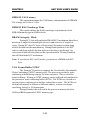
1
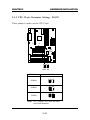
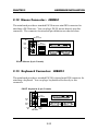
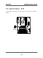
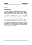
CHAPTER 1 INTRODUCTION Chapter 1 INTRODUCTION The MS-6112 is a high-performance personal computer mainboard based on the Pentium® II processor. The mainboard uses the highly integrated Intel® 82440LX AGPset which optimize the system bandwidth and concurrency with the implementation of Quad Port Acceleration (QPA). QPA provides 4-port concurrent arbitration of the processor bus, graphics, PCI bus and SDRAM. The Intel® 82371AB chipset integrates all system control functions such as ACPI (Advanced Configuration and Power Interface). The ACPI provides more Energy Saving Features for the OSPM(OS Direct Power Management) function. The Intel® 82371AB chipset also improves the IDE transfer rate by supporting Ultra DMA/33 IDE that transfers data at the rate of 33MB/s. The mainboard also supports the LM78 System Hardware Monitor Controller as optional function. The LM78 function includes: CPU /power supply/chassis fan revolution detect, CPU/system voltage monitor, system temperature monitor, and chassis intrusion detect(optional). 1-1 CHAPTER 1 INTRODUCTION 1.1 Mainboard Features CPU l l l Slot 1 for Pentium® II processor Supports 200MHz, 233MHz, 266MHz, 300MHz, and 333MHz. Core/Bus ratios are x2, x2.5, x3, x3.5, x4, x4.5, x5, x5.5, x6 and higher. Switching Voltage Regulator l On-board switching mode DC-DC Step Down Regulator. l Conforms to Intel® VRM ver 8.1 specifications. l Over-Voltage and Over-Current protection. Chip Set l Intel ® 82440LX PCI Chipset. Clock Generator l 66.6MHz clocks are supported. Main Memory l Supports six memory banks using three 168-pin unbuffered DIMM sockets. l Supports a maximum memory size of 512MB with SDRAM, or 1GB with EDO. l Supports ECC(Error Check Correct) and EC(Multiple-Bit Error Correction) function. l Supports 3.3v Extended Data Output (EDO) and SDRAM DIMM. Slots l One AGP(Accelerated Graphics Port) slot. - AGP specification compliant - AGP 66/133MHz 3.3v device support l Three 32-bit Master PCI Bus slots and four 16-bit ISA bus slots wherein one shared slot that can be used as ISA or PCI. l Supports 3.3v/5v PCI bus Interface. 1-2 CHAPTER 1 INTRODUCTION On-Board IDE l An IDE controller on the Intel ® 82371AB PCI Chipset provides IDE HDD/ CD-ROM with PIO, Bus Master and Ultra DMA/33 operation modes. l Can connect up to four IDE devices. On-Board Peripherals l On-Board Peripherals include: - 1 floppy port supports 2 FDD with 360K, 720K, 1.2M, 1.44M and 2.88Mbytes. - 2 serial ports (COMA + COMB) - 1 parallel port supports SPP/EPP/ECP mode - 2 USB ports - 1 IrDA connector for SIR. BIOS l The mainboard BIOS provides “Plug & Play” BIOS which detects the peripheral devices and expansion cards of the board automatically. l The mainboard provides a Desktop Management Interface(DMI) function which records your mainboard specifications. On-Board System Hardware Monitor(LM78) l CPU/Power Supply/Chassis Fan Revolution Detect l CPU Fan Control (the fan will automatically stop when the system enters suspend mode) l System Voltage Detect l Chassis Intrusion Detect(reserved) l Display Actual Current Voltage RTC l Non-Volatile RTC. Keyboard Connector l PS/2® keyboard interface and PS/2® mouse interface. 1-3 CHAPTER 1 INTRODUCTION Dimension l ATX Form Factor: 30cm(L) x 23cm(W) x 4 layers PCB. l Double deck I/O connectors, compatible with Intel ® Venus Mainboard. Mounting l 9 mounting holes. 1-4 CHAPTER 1 INTRODUCTION 1.2 Mainboard Layout PSFAN1 USB Top: Port 1 Bottom: Port 2 ATX Power Supply Top: mouse Bottom: keyboard LM75 (optional) LM78 (optional) CFAN1 SLOT 1 Top: LPT Bottom: COM A COM B JSW1 DIMM 1 DIMM 2 IR1 DIMM 3 FW82443LX 1 AGP J3 J4 PCI SLOT 1 Chassis Intrusion Sensor (optional) IDE1 IDE2 FDC JFAN Clock Generator J10 J9 BATT PCI SLOT 2 JFP1 + SW1 FW82371AB PCI SLOT 3 JSW2 JGL1 JBAT1 ISA SLOT BIOS KBC JLG1 ISA SLOT ISA SLOT JMODE1 ISA SLOT SFAN1 MS-6112 1-5 CHAPTER 2 HARDWARE INSTALLATION Chapter 2 HARDWARE INSTALLATION 2.1 Central Processing Unit: CPU The mainboard operates with Intel® Pentium® II processor. The mainboard uses a CPU Slot called Slot 1 for easy CPU installation and a DIP switch (SW1) to set the proper speed for the CPU. The CPU should always have a Heat Sink and a cooling fan attached to prevent overheating. 2-1 CHAPTER 2 HARDWARE INSTALLATION 2.1-1 CPU Installation Procedures There are two kinds of Pentium® II processor that is currently used: the OEM Pentium® II processor and the Boxed Pentium ® II processor. OEM Pentium® II processor has no Heat Sink, Fan and Heat Sink Support, while the Boxed Pentium® II processor is provided with Heat Sink w/ fan and Heat Sink Support. A. OEM Pentium® II processor Installation Procedures Processor Lock Heat Sink W/Fan Pentium® II Processor Notch Hole Retention Mechanism Heat Sink Support Top Bar Heat Sink Support Base Heat Sink Support Pin Required Things: Pentium® II processor - Processor. *Retention Mechanism(RM) - Plastic Guide that holds the S.E.C. Catridge in the Slot 1 connector. *Retention Mechanism Attach Mount(RMAM) - Bolt/Bridge assemblies inserted up through the bottom of the motherboard. RM secures to RMAM ( 2 RMAM required per RM ). *Heat Sink Support Base (HSSBASE) - Plastic support bar mounted to the mainboard under the ATX heatsink. (One leg is always bigger than the other one) 2-2 CHAPTER 2 HARDWARE INSTALLATION *Heat Sink Support Pin (HSSPIN) - Plastic pins inserted through the HSSBASE to secure it to the mainboard (2 required per Assembly). *Heat Sink Support Top Bar (HSSTOP) - Plastic bar that clips onto the HSSBASE through the fins on the ATX heatsink. **Heat Sink w/ fan - Heat Sink that can be attached to the Pentium® II processor with metal clip. Note: * Provided by MSI mainboard. ** Provided by Special request. HSSBASE RM HSSPIN RMAM HSSTOP 2-3 CHAPTER 2 HARDWARE INSTALLATION Step 1: Insert the Retention Mechanism Attach Mount at the bottom of the mainboard. Step 2: Install the Retention Mechanism. Look for the key on Slot 1, and match it with the Notch Key on the Retention Mechanism for proper direction. Then, attach the Retention Mechanism to the Retention Mechanism Attach Mount. Use a Screwdriver to secure the Retention Mechanism. Retention Mechanism ê Retention Mechanism Attach Mount ê ê Notch Key Key SLOT1 2-4 ê CHAPTER 2 HARDWARE INSTALLATION Step 3: Install the Heat Sink Support Base. Look for the Two holes across Slot 1, and match it with the Two legs of the Heat Sink Support Base for the proper direction. Take note that one hole/leg is bigger than the other. The Four top pins of the Heat Sink Support Base should also be oriented towards Slot 1. pins Heat Sink Support Pin Leg Heat Sink Support Base Push the Heat Sink Support Base onto the mainboard, until you hear a click sound. Check for a perfect fit. Step 4: Install the Heat Sink Support Pin. Push the Heat Sink Support Pins onto the two holes of the Heat Sink Support Base. Check for a perfect fit. These pins are used to secure the Heat Sink Support Base. 2-5 CHAPTER 2 HARDWARE INSTALLATION Step 5: Install the Heat Sink with Fan to the Processor. Push down the metal clips, so that they are in line with the back of the Heat Sink. Be careful, so as not detach the metal clips from the Heat Sink. Heat Sink w/ Fan arrow â The should be pointing down. Heat Sink Base Holder Metal Clips In case the metal clips are detached from the Heat Sink, re-attach them. Look for the arrow on the metal clip. This arrow should be pointing down and aligned with the Heat Sink Support Base Holder. Attach the Heat Sink to the processor. Metal Clips Ear Clip Holder Secure Posts Secure holes Clip Holder S.E.C. Cartridge - Thermal P Isometric View N tT S l Metal Clips Ear Pentium ® II processor (Back) Heat Sink w/ Fan(Back) - Look at the back of the Heat Sink and take note of the 2 secure posts. Insert these 2 Secure posts to the 2 secure holes on the back of the processor. - Align the ears of the metal clips with the clip holders on the back of the processor. Use a screw driver to push the metal clips onto the clip holders. Check for a perfect fit. 2-6 CHAPTER 2 HARDWARE INSTALLATION Step 6: Install the Processor. Unlock the Processor by pushing in the Processor Locks. è ç Insert the Processor like inserting a PCI or an ISA card. Step 7: Lock the Processor Locks. Secure the CPU by pulling the Processor Locks out. è ç 2-7 CHAPTER 2 HARDWARE INSTALLATION Step 8: Install the Heat Sink Support Top Bar. Push the Heat Sink Support Top Bar to the Heat Sink Support Base, Until you hear a “click” sound. Check for a perfect fit. Heatsink Support Top Bar The installation is now complete. 2-8 CHAPTER 2 HARDWARE INSTALLATION B. Boxed Pentium® II processor Installation Procedures The Boxed Pentium® II processor has a built- in Fan and Heat Sink. It also has a Heat Sink Support. So if you’re going to use the Boxed processor, all you need is the Retention Mechanism. Step 1: Insert the Retention Mechanism Attach Mount at the bottom of the mainboard. Step 2: Install the Retention Mechanism. Look for the key on Slot 1, and match it with the Notch Key on the Retention Mechanism for proper direction. Then, attach the Retention Mechanism to the Retention Mechanism Attach Mount. Use a Screwdriver to secure the Retention Mechanism. Retention Mechanism ê Retention Mechanism Attach Mount ê ê Notch Key Key SLOT1 2-9 ê CHAPTER 2 HARDWARE INSTALLATION Step 3: Install the Heat Sink Support Base. Look for the 2 holes across Slot 1, and match it with the 2 Heat Sink Support Base. Take note that one hole/base is bigger than the other. Retention Mechanism Notch Hole PC-3742 Heat Sink Support Base Push the Heat Sink Support Base onto the mainboard, until you hear a click sound. Check for a perfect fit. 2-10 CHAPTER 2 HARDWARE INSTALLATION Step 4: Install the Heat Sink Support. Attach the 2 Heat Sink Supports to the sides of the Processor. These Heat Sink Supports will fit in any direction, so be sure that the Heat Sink Support Locks are oriented outwards for the proper direction. Intel® Boxed PentiumTM II Processor Heat Sink Support PC-3743 Heat Sink Support Lock 2-11 CHAPTER 2 HARDWARE INSTALLATION Step 5: Unlock the Processor Locks and Heat Sink Support Locks. Push in the Processor Locks. Open the Heat Sink Support Locks. Processor Lock Heatsink Support Lock PC-3744 Step 6: Insert the Processor like inserting a PCI or an ISA card. 2-12 CHAPTER 2 HARDWARE INSTALLATION PC-3745 Step 7: Lock the Processor Locks and Heat Sink Support Locks Secure the CPU by pushing out the Processor Locks. Close the Heat Sink Support Locks. The installation is now complete. 2-13 CHAPTER 2 HARDWARE INSTALLATION 2.1-2 CPU Speed Setting: SW1 To adjust the speed of the CPU, you must know the spec. of your CPU (always ask the vendor for CPU spec.). Then look at Table 2.1 (200 ~ 333MHz Intel® Pentium® II processor) for setting. 1 2 3 4 OFF SW1 ON ON DIP Speed Setting CPU Type SW1 DIP 2 ON 1 ON 3 4 DIP 2 ON 1 4 3 4 DIP 2 3 4 DIP ON 1 OFF ON ON 333MHz DIP OFF 3 300MHz ON 2 OFF 1 266MHz ON ON 4 OFF 3 233MHz ON 2 OFF 1 200MHz Table 2.1 200 ~ 333MHz Intel ® Pentium ® II processor 2-14 CHAPTER 2 HARDWARE INSTALLATION 2.1-3 CPU Clock Generator Setting: J10/J9 These jumper is used to set the CPU Clock. J10 J9 CPU Clock J10 J9 66 MHz 68 MHz 75 MHz Note: 68/75 MHz CPU clock are both reserved function. 2-15 CHAPTER 2 HARDWARE INSTALLATION 2.1-4 CPU Fan Power Connectors: JFAN/CFAN1/SFAN1/ PSFAN1 These connectors support system cooling fan with +12V. It supports three pin head connector. When connecting the wire to the connector, always take note that the red wire is the positive and should be connected to the +12V, the black wire is Ground and should be connected to GND. If your mainboard has LM78 chipset on-board, you must use a specially designed fan with speed sensor to take advantage of LM78’s CPU fan control. GND GND +12V +12V SENSOR PSFAN1 SENSOR CFAN1 GND +12V GND JFAN GND +12V SENSOR PSFAN1 : Power Supply Fan CFAN1 : CPU Fan SFAN1 : System(Chassis) Fan SFAN1 For fans with fan speed sensor, every rotation of the fan will send out 2 pulses. LM78 will count and report the fan rotation speed. Note: 1. CFAN1/SFAN1/PSFAN1 are the CPU, Power and Chassis Cooling Fan Speed Connector (reserved for LM78 System Hardware Monitor Option.) 2. Always consult vendor for proper CPU cooling fan. 2-16 CHAPTER 2 HARDWARE INSTALLATION 2.2 Flash ROM Programming Voltage: JMODE1 This jumper is for setting the Voltage of the Flash ROM BIOS. 1 3 JMODE1 Voltage Setting JMODE1 JMODE1 +12V 1 PWD VCC 1 +12V PWD VCC 3 3 +5V +12V (default) Note: Short 1-2 pin, if you’re using Intel® or flash memory and you want to flash the ROM data. 2-17 CHAPTER 2 HARDWARE INSTALLATION 2.3 External Battery Connector: JBAT1 A battery must be used to retain the mainboard configuration in CMOS RAM. If you use the on-board battery, you must short 1-2 pins of JBAT1 to keep the CMOS data. 1 3 JBAT1 1 1 3 3 Clear Data Keep Data Note: You can clear CMOS by shorting 2-3 pin, while the system is off. Then, return to 1-2 pin position. Avoid clearing the CMOS while the system is on; it will damage the mainboard. 2-18 CHAPTER 2 HARDWARE INSTALLATION 2.4 Memory Installation 2.4-1 Memory Bank Configuration The mainboard supports a maximum of 1 GB of memory for EDO and 512MB for SDRAM: It provides three 168-pin unbuffered DIMMs (Double In-Line Memory Module) sockets. It supports 8 MB to 256 Mbytes DIMM memory module. The memory module can be either SDRAM or EDO (Extended Data Output) Mode DRAM. A DIMM consists of two Banks and may have a maximum of 256 MB of memory. 2-19 DIMM1(Bank0 + Bank1) DIMM2(Bank2 + Bank3) DIMM3(Bank4 + Bank5) Note: FP(Fast Page) & BEDO(Burst EDO) are not supported. CHAPTER 2 HARDWARE INSTALLATION 2.4-2 Memory Installation Procedures A. How to install a DIMM Module Single Sided DIMM Double Sided DIMM 1. The DIMM slot has a two Notch Key “VOLT and DRAM”, so the DIMM memory module can only fit in one direction. 2. Insert the DIMM memory module vertically into the DIMM slot. Then push it in. DRAM VOLT 3. Close the plastic clip at the side of the DIMM slot. Note: You can only use a 3.3 volt DIMM module (EDO or SDRAM). 2-20 CHAPTER 2 HARDWARE INSTALLATION 2.4-1 Memory Population Rules 1. Supports EDO and SDRAM. 2. Supports unbuffered DIMM. 3. To operate properly, at least one 168-pin DIMM module must be installed. 4. This mainboard supports Table Free memory, so memory can be installed on DIMM1, DIMM2, or DIMM 3 in any order. 5. Supports 3.3 volt DIMM. 6. The DRAM addressing and the size supported by the mainboard is shown next page. 2-21 CHAPTER 2 HARDWARE INSTALLATION Table 2.4-1 EDO DRAM Memory Addressing DRAM Tech. 4M 16M 64M DRAM DRAM Density & Addressing Width 1Mx4 SYMM 1Mx16 SYMM 1Mx16 ASYM 2Mx8 ASYM 2Mx8 ASYM 4Mx4 SYMM 4Mx4 ASYM 2Mx32 ASYM 2Mx32 ASYM 2Mx32 ASYM 4Mx16 SYMM 4Mx16 ASYM 8Mx8 ASYM 16Mx4 SYMM Address Size Row Column 10 10 12 11 12 11 12 11 12 13 11 12 12 12 10 10 8 10 9 11 10 10 9 8 11 10 11 12 MB/SIMM Single no. Double no. Side(S) pcs. Side(D) pcs. 4MBx8 8MBx16 4MBx2 8MBx4 4MBx2 8MBx4 8MBx4 16MBx8 8MBx4 16MBx8 16MBx8 32MBx16 16MBx8 32MBx16 8MBx1 16MBx2 8MBx1 16MBx2 8MBx1 16MBx2 16MBx2 32MBx4 16MBx2 32MBx4 32MBx4 64MBx8 64MBx8 128MBx16 Table 2.4-2 SDRAM Memory Addressing DRAM Tech. 16M 64M 64M DRAM DRAM Density & Addressing Width 1Mx16 ASYM 2Mx8 ASYM 4Mx4 ASYM 2Mx32 ASYM 2Mx32 ASYM 4Mx16 ASYM 4Mx16 ASYM 8Mx8 ASYM 16Mx4 ASYM 2Mx32 ASYM 4Mx16 ASYM 8Mx8 ASYM 16Mx4 ASYM Address Size Row Column 11 11 11 11 12 11 13 13 13 11 12 12 12 8 9 10 9 8 10 8 9 10 8 8 9 10 2-22 MB/DIMM Single no. Double no. Side(S) pcs. Side(D) pcs. 8MBx4 16MBx8 16MBx8 32MBx16 32MB 64MB 32MBx2 64MBx4 16MBx2 32MBx4 32MB 64MB 32MB 64MB 64MB 128MB 128MB 256MB CHAPTER 2 HARDWARE INSTALLATION 2.5 Case Connector: JFP1 The Turbo LED, Reset Switch, Key Lock, Power LED, Speaker and HDD LED are all connected to the JFP1 connector block. Keylock + Power LED Turbo LED + Speaker Reset Switch + HDD LED JFP1 2-23 CHAPTER 2 HARDWARE INSTALLATION 2.5-1 Turbo LED The Turbo LED is always ON. You can connect the Turbo LED from the system case to this pin. 2.5-2 Reset Switch Reset switch is used to reboot the system rather than turning the power ON/ OFF. Avoid rebooting while the HDD LED is lit. You can connect the Reset switch from the system case to this pin. 2.5-3 Keylock Keylock allows you to disable the keyboard for security purposes. You can connect the keylock to this pin. 2.5-4 Power LED The Power LED is always lit while the system power is on. You can connect the Power LED from the system case to this pin. 2.5-5 Speaker Speaker from the system case is connected to this pin. 2.5-6 HDD LED HDD LED shows the activity of a hard disk drive. Avoid turning the power off while the HDD led is lit. You can connect the HDD LED from the system case to this pin. 2-24 CHAPTER 2 HARDWARE INSTALLATION 2.6 Floppy Disk Connector: FDC The mainboard also provides a standard floppy disk connector FDC that supports 360K, 720K, 1.2M, 1.44M and 2.88M floppy disk types. This connector support the provided floppy drive ribbon cables. FDC 1 2-25 CHAPTER 2 HARDWARE INSTALLATION 2.7 Hard Disk Connectors: IDE1 & IDE2 Primary IDE Connector Secondary IDE Connector The mainboard has a 32-bit Enhanced PCI IDE Controller that provides PIO mode 0~4, Bus Master, and Ultra DMA/33 function. It has two HDD connectors IDE1 (primary) and IDE2 (secondary). You can connect up to four hard disk drives, CD-ROM, 120MB Floppy (reserved for future BIOS) and other devices to IDE1 and IDE2. These connectors support the provided IDE hard disk cable. 1 1 IDE1(Primary IDE Connector) The first hard drive should always be connected to IDE1. IDE1 can connect a Master and a Slave drive. You must configure second hard drive to Slave mode by setting the jumper accordingly. IDE2(Secondary IDE Connector) IDE2 can also connect a Master and a Slave drive. 2-26 CHAPTER 2 HARDWARE INSTALLATION 2.8 Power Supply 2.8-1 ATX 20-pin Power Connector: JPWR1 This connector supports the power button on-board. Using the ATX power supply, functions such as Modem Ring Wake-Up and Soft Power Off are supported by this mainboard. 10 20 ATX Power Connector 1 11 PIN DEFINITION PIN 1 2 3 4 5 6 7 8 9 10 PIN 11 12 13 14 15 16 17 18 19 20 SIGNAL 3.3V 3.3V GND 5V GND 5V GND PW_OK 5V_SB 12V 2-27 SIGNAL 3.3V -12V GND PS_ON GND GND GND -5V 5V 5V CHAPTER 2 HARDWARE INSTALLATION 2.8-2 Remote Power On/Off Switches: JSW1/JSW2 Connect to a 2-pin push button switch. Every time the switch is shorted by pushing it once, the power supply will change its status from OFF to ON. During ON stage, push once and the system goes to sleep mode: pushing it more than 4 seconds will change its status from ON to OFF. If you want to change the setup, you could go to the BIOS Power Management Setup. This is used for ATX type power supply. JSW1 JSW2 Note: The two switches are provided by the mainboard for your convenience, so you can use any of them. The two switches have the same feature. 2-28 CHAPTER 2 HARDWARE INSTALLATION 2.9 IrDA Infrared Module Connector: IR1 The mainboard provides two 5-pin infrared (IR) connectors for IR modules. These connectors are for optional wireless transmitting and receiving infrared module. You must configure the setting through the BIOS setup to use the IR function. FIR and Consumer IR are reserved functions. 1 VCC NC IRRX GND IRTX IR1 2-29 CHAPTER 2 HARDWARE INSTALLATION 2.10 Serial Port Connectors: COM A & COM B The mainboard has two 9-pin male DIN connectors for serial ports COM A and COM B. These two ports are 16550A high speed communication ports that send/receive 16 bytes FIFOs. You can attach a mouse or a modem cable directly into these connectors. 1 2 3 4 5 6 7 8 9 COM A COM B PIN DEFINITION PIN SIGNAL 1 DCD(Data Carry Detect) 2 SIN(Serial In or Receive Data) 3 SOUT(Serial Out or Transmit Data) 4 DTR(Data Terminal Ready) 5 GND 6 DSR(Data Set Ready) 7 RTS(Request To Send) 8 CTS(Clear To Send) 9 RI(Ring Indicate) 2-30 CHAPTER 2 HARDWARE INSTALLATION 2.11 Parallel Port Connector: LPT The mainboard provides a 25 pin female centronic connector for LPT. A parallel port is a standard printer port that also supports Enhanced Parallel Port(EPP) and Extended capabilities Parallel Port(ECP). See connector and pin definition below: LPT 13 12 11 10 9 8 7 6 5 4 3 2 1 25 24 23 22 21 20 19 18 17 16 15 14 PIN DEFINITION PIN 1 2 3 4 5 6 7 8 9 10 11 12 13 SIGNAL STROBE DATA0 DATA1 DATA2 DATA3 DATA4 DATA5 DATA6 DATA7 ACK# BUSY PE SELECT PIN 14 15 16 17 18 19 20 21 22 23 24 25 2-31 SIGNAL AUTO FEED# ERR# INIT# SLIN# GND GND GND GND GND GND GND GND CHAPTER 2 HARDWARE INSTALLATION 2.12 Mouse Connector: JKBMS1 The mainboard provides a standard PS/2® mouse mini DIN connector for attaching a PS/2®mouse. You can plug a PS/2® mouse directly into this connector. The connector location and pin definition are shown below: Pin6 NC Pin4 VCC Pin5 Mouse Clock Pin3 GND Pin1 Mouse DATA Pin2 NC PS/2® Mouse (6-pin Female) 2.13 Keyboard Connector: JKBMS1 The mainboard provides a standard PS/2® keyboard mini DIN connector for attaching a keyboard. You can plug a keyboard cable directly to this connector. PS/2® Keyboard (6-pin Female) Pin5 KBD Clock Pin6 NC Pin4 VCC Pin2 NC Pin3 Pin1 GND KBD DATA 2-32 CHAPTER 2 HARDWARE INSTALLATION 2.14 USB Connector: USB The mainboard provides a UHCI(Universal Host Controller Interface) Universal Serial Bus root for attaching USB devices like: keyboard, mouse and other USB devices. You can plug the USB device directly to this connector. USB Port 1 1 2 3 4 USB Port 2 PIN 1 2 3 4 SIGNAL VCC -Data0 GND +Data0 2-33 CHAPTER 2 HARDWARE INSTALLATION 2.15 Power Saving LED Connector: JGL1 JGL1 can be connected with LED. This will lit while the system is in suspend mode. JGL1 2-34 CHAPTER 2 HARDWARE INSTALLATION 2.16 Special Jumpers: J3/J4 These jumper is used only by special customer. Always leave it on default setting. 3 1 J3 J4 (default) 2-35 CHAPTER 3 AMI® BIOS USERS GUIDE Chapter 3 AMI® BIOS USER GUIDE The system configuration information and chipset register information is stored in the CMOS RAM. This information is retained by a battery when the power is off. Enter the BIOS setup (if needed) to modify this information. The following pages will describe how to enter BIOS setup, and all about options. 3-1 CHAPTER 3 AMI® BIOS USERS GUIDE 3.1 Enter BIOS Setup Enter the AMI® setup Program’s Main Menu as follows: 1. Turn on or reboot the system. The following screen appears with a series of diagnostic check. AMIBIOS (C) 1996 American Megatrends Inc. AGIOMS VXXX XXXXXX Hit <DEL> if you want to run setup (C) American Megatrends Inc. 61-XXXX-001169-00111111-071592-i82440FX-H 2. When the “Hit <DEL>” message appears, press <DEL> key to enter the BIOS setup screen. 3. After pressing <DEL> key, the BIOS setup screen will appear. Note: If you don’t want to modify CMOS original setting, then don’t press any key during the system boot. 3-2 CHAPTER 3 AMI® BIOS USERS GUIDE AMIBIOS HIFLEX SETUP UTILITIES - VERSION 1.07 (C) 1996 American Megatrends, Inc. All Rights Reserved Standard CMOS Setup Advanced CMOS Setup Advanced Chipset Setup Power Management Setup PCI/Plug and Play Setup Peripheral Setup Hardware Monitor Setup Auto-Detect Hard Disks Change User Password Change Supervisor Password Change Language Setting Auto Configuration with Optimal Settings Auto Configuration with Fail Safe Settings Save Settings and Exit Exit without Saving Standard CMOS setup for changing time, hard disk type, etc. 4. Use the <Up> and <Down> key to move the highlight scroll up or down. 5. Use the <ENTER> key to select the option. 6. To exit, press <ESC>. To save and exit, press <F10>. 7. Section 3.2 to 3.7 will explain the option in more details. 3-3 CHAPTER 3 AMI® BIOS USERS GUIDE 3.2 Standard CMOS Setup 1. Press <ENTER> on “Standard CMOS Setup” of the main menu screen . AMIBIOS SETUP - STANDARD CMOS SETUP (C)1996 American Megatrends,Inc.All Rights Reserved Date (mm/dd/yyyy): Mon Jul 28, 1997 Time (hh/mm/ss): 17:09:25 Floppy Drive A: Floppy Drive B: Pri Pri Sec Sec Master Slave Master Slave Type :Auto :Auto :Auto :Auto 1.44 MB 3 1/2 Not Installed Size Cyln Head WPcom Sec LBA Mode ON ON ON ON Blk Mode ON ON ON ON PIO Mode AUTO AUTO AUTO AUTO 32Bit Mode ON ON ON ON Boot Sector Virus Protection Disabled Month Day Year : Jan-Dec : 01-31 : 1901-2099 ESC:Exit :Sel PgUp/PgDn:Modify F2/F3:Color 2. Use <Up> and <Down> to choose the item and <PgUp> and <PgDn> keys to modify the highlighted item. 3. After you have finished with the Standard CMOS Setup, <ESC> to go back to the main menu. 3-4 press CHAPTER 3 AMI® BIOS USERS GUIDE 3.3 Advanced CMOS Setup 1. Press <ENTER> on “Advanced CMOS Setup” of the main menu AMIBIOS SETUP - ADVANCED CMOS SETUP (C) 1996 American Megatrends, Inc. All Rights Reserved Quick Boot Ist Boot Device 2nd Boot Device 3rd Boot Device Try Other Boot Devices Initial Display Mode Display Mode At ADD-ON ROM Init Floppy Access Control Hard Disk Access Control BootUp Num-Lock Floppy Drive Swap Floppy Drive Seek PS/2 Mouse Support Primary Display Password Check Parity Check Boot to OS/2 64M System BIOS Cacheable C000, 16k Shadow C400, 16k Shadow C800, 16k Shadow CC00, 16k Shadow D000, 16k Shadow D400, 16k Shadow D800, 16k Shadow DC00, 16k Shadow Enabled Floppy IDE 0 CD-ROM Yes BIOS Force BIOS Read-Write Read-Write On Disabled Disabled Enabled Abset Setup Disabled No Enabled Cached Cached Disabled Disabled Disabled Disabled Disabled Disabled Available Options: Enabled Disabled ESC:Exit :Sel PgUp/PgDn:Modify F2/F3:Color 2. Use <Up> and <Down> to choose the item and <PgUp> and <PgDn> keys to modify the highlighted item. 3. After you have finished with the Advanced CMOS Setup, press <ESC> to go back to the main menu. 3-5 CHAPTER 3 AMI® BIOS USERS GUIDE Description of the item on screen follows: Quick Boot Set this option to Enabled to permit AMI® BIOS to boot within 5 seconds. This option replaces the old ABOVE 1 MB Memory Test option. The Optimal default setting is Enabled. The Fail-Safe default setting is Disabled. 1st Boot Device/2nd Boot Device/3rd Boot Device This option sets the sequence of boot drives. The settings are: IDE0 The system will boot from the first HDD. IDE1 The system will boot from the Second HDD. IDE2 The system will boot from the Third HDD. IDE3 The system will boot from the Fourth HDD. F(optical) The system will boot from LS-120(120M Floppy). SCSI The system will boot from the SCSI. Network The system will boot from the Network drive. CD-ROM The system will boot from the CD-ROM. Disable Disable this sequence. Try other Boot Devices This option sets the device boot, if all the Four Boot Devices failed. Floppy Access Control This option sets the Floppy to Read-only or Read-Write. HDD Access Control This option sets the HDD to Read-only or Read-Write. During Read-only, if you try to write on the HDD, the system will halt. 3-6 CHAPTER 3 AMI® BIOS USERS GUIDE Boot up Num Lock When this option is set to Off, AMI® BIOS turns off the Num Lock key when the system is powered on. The end user can then use the arrow keys on both the numeric keypad and the keyboard. The settings are On or Off. The optimal default and Fail-Safe default settings are On. Floppy Drive Swap Set this option to Enabled to specify that floppy drives A: and B: are swapped. The setting are Enabled and Disabled. The Optimal and FailSafe default settings are Disabled. Floppy Drive Seek When this option is set to Enabled, AMI® BIOS performs a Seek command on floppy drive A: before booting the system. The settings are Enabled and Disabled. The Optimal and Fail-Safe default settings are Disabled. PS/2® Mouse Support When this option is set to Enabled, AMI® BIOS supports a PS/2®type mouse. The settings are Enabled and Disabled. The Optimal and FailSafe default settings are Enabled. Primary Display This option configures the primary display subsytem in the computer. The settings are Mono(monochrome), 40CGA, 80CGA or VGA/ EGA. The optimal and Fail-Safe default settings are VGA/EGA. Password Check This option specifies the type of AMI® BIOS password protection that is implemented. The Optimal and Fail-Safe default settings are Setup. 3-7 CHAPTER 3 AMI® BIOS USERS GUIDE Parity Check Set this option to Enabled to use the Parity Check function. The DIMM module need to have parity bit for this function to work. Boot to OS/2® Set this option to Enabled to permit the BIOS to run properly, if OS/2® is to be used with > 64MB of DRAM. The settings are Enabled or Disabled. The Optimal and Fail-safe default settings are Disabled. Internal Cache/External Cache This option selects the type of caching algorithm used by AMI® BIOS and the CPU for L1 cache memory(internal/external to the CPU). The settings are Writeback - a writeback algorithm is used, Write-through - a write-through algorithm is used or Disabled - AMI® BIOS does not specify the type of caching algorithm. The algorithm is set by the CPU. The Optimal and Fail-Safe default settings are Writeback. System BIOS Cacheable AMI® BIOS always copies the system BIOS from ROM to RAM for faster execution. Set this option to Enabled to permit the contents of the F0000h RAM memory segment to be written to and read from cache memory. The settings are Enabled or Disabled. The Optimal default setting is Enabled. The Fail-Safe default setting is Disabled. C000, 16K Shadow/C400, 16k Shadow These options specify how the contents of the video ROM are handled. The settings are: Disabled - the Video ROM is not copied to RAM. Cached -the contents of the video ROM from C0000h C7FFFh are not only copied from ROM to RAM; it can also be written to or read from cache memory. Shadow - the Contents of the video ROM from C0000h C7FFFh are copied(shadowed) from ROM to RAM for faster execution. The Optimal and Fail-Safe default setting is Cached. 3-8 CHAPTER 3 AMI® BIOS USERS GUIDE C800, 16k Shadow/CC00, 16k Shadow/D000, 16K Shadow/ D400, 16k Shadow/D800, 16k Shadow/DC00, 16K Shadow These options specify how the contents of the adaptor ROM named in the option title are handled. The ROM area that is not used by ISA adapter cards will be allocated to PCI adapter cards. The settings are; Disabled - The specified ROM is not copied to RAM. Cache - The contents of the ROM area are not only copied from ROM to RAM for faster execution, it can also be written to or read from cache memory. Shadow - The contents of the ROM area are copied from ROM to RAM for faster execution. The Optimal and Fail-Safe default settings are Disabled. 3-9 CHAPTER 3 AMI® BIOS USERS GUIDE 3.4 Advanced Chipset Setup 1. Press <ENTER> on “Advanced Chipset Setup” of the main menu screen. AMIBIOS SETUP - ADVANCED CHIPSET SETUP (C) 1996 American Megatrends, Inc. All Rights Reserved Auto Configure EDO DRAM Timing EDO DRAM Speed (ns) EDO Read Burst Timing EDO Write Burst Timing EDO RAS Precharge Timing EDO RAS to CAS Delay MA wait State ***** SDRAM Timing ***** SDRAM RAS to CAS Delay SDRAM CAS Latency SDRAM RAS Precharge Time DRAM Integrity Mode VGA Frame Buffer USWC PCI Frame Buffer USWC Fixed Memory Hole CPU To PCI IDE Posting USWC Write I/O Post AGP Aperture Size USB Passive Release PIIX4 Passive Release PIIX4 Delayed Transaction USB Function USB Keyboard Legacy Support Enabled 60 x222 x222 3 clocks 3 clocks Slow Available Options: Enabled Disabled 2 Clks 3 Clks 2 Clks Non ECC Disabled Disabled Disabled Enabled Disabled 64 MB Enabled Enabled Enabled Enabled Disabled ESC:Exit :Sel PgUp/PgDn:Modify F2/F3:Color 2. Use <Up> and <Down> to choose the item and <PgUp> and <PgDn> keys to modify the highlighted item. 3. After you have finished with the Advanced Chipset Setup, press <ESC> to go back to the main menu. 3-10 CHAPTER 3 AMI® BIOS USERS GUIDE Description of the item on screen follows: Auto Configure EDO DRAM Timing Choose Enabled(default) will automatically configure the DRAM timing depending on the “DRAM Speed” selection. Choose disable to customize setup. EDO DRAM Speed (ns) This option specifies the RAS access time (in nanoseconds) for the DRAM used in the computer. The settings are 50,60 or 70. The Optimal default setting is 60 and the Fail-Safe default setting is 70. EDO DRAM Read Burst Timing Choose DRAM read burst timing for the customize setup. B stand for BEDO DRAM, E stand for EDO DRAM and F stand for FAST PAGE DRAM. EDO DRAM Write Burst Timing Choose DRAM write burst timing for the customize setup. EDO RAS Precharge Timing This option defines the RAS# precharge requirements for the EDO memory type in 66MHz clocks. EDO RAS to CAS Delay This operation decide the delay in assertion of CAS#(SCAS#) from assertion of RAS#(SRAS#) in 66MHz. MA Wait State This option selects Fast or Slow MA bus timing. The Slow timing is equal to Fast+1, in term of clock number for EDO DRAM. SDRAM RAS to CAS Delay This operation decide the delay in assertion of CAS#(SCAS#) from assertion of RAS#(SRAS#) in 66MHz. 3-11 CHAPTER 3 AMI® BIOS USERS GUIDE SDRAM CAS Latency This option determines the CAS latency time parameter of SDRAM. The settings are 2 clks or 3 clks. SDRAM RAS Precharge Time This option defines the RAS# precharge requirements for the SDRAM memory type in 66MHz clocks. DRAM Integrity Mode During ECC, this will enable the DRAM ECC mechanism that allows detection of single-bit and multiple-bit errors and recovery of single-bit errors. During EC, the ECC logic will calculate 8-bit pattern written along with 64-bit data into the main memory. During Read operation, 8-bit ECC code is read along with 64-bit data and error checking is performed. No correction of data will take place in this operation mode. During Disabled, this will disable the ECC mechanism. Note: If you choose ECC or EC modes, you must use a DIMM with ECC byte. VGA Frame Buffer USWC The Pentium® II processor supports the Uncacheable Speculatable Write-Combining (USWC) memory type. The processor provides a writecombining with buffering strategy for write operation. This is useful for frame buffering. Writing to USWC memory can be buffered and combined in the processors write-combining buffer (WCB). The WCBs are viewed as a special purpose outgoing write buffers, rather than a cache. The WCBs are written into memory to allocate a different address, or after executing a serializing, locked, or I/O instructions. During Enabled, this will enable the processor memory location A000 and B000 segment as USWC memory type. 3-12 CHAPTER 3 AMI® BIOS USERS GUIDE PCI Frame Buffer USWC The Pentium® II processor supports the Uncacheable Speculatable Write-Combining (USWC) memory type. The processor provides a writecombining with buffering strategy for write operation. This is useful for frame buffering. Writing to USWC memory can be buffered and combined in the processors write-combining buffer (WCB). The WCBs are viewed as a special purpose outgoing write buffers, rather than a cache. The WCBs are written into memory to allocate a different address, or after executing a serializing, locked, or I/O instructions. During Enabled, this will enable the processor memory location C000 and DFFF segment as USWC memory type. DRAM Refresh Queue Choose Enabled, the system will provide 4-deep refresh queue. All refresh request are queued, with the 4th refresh request being the priority request. All refresh requests are priority when the refresh queue is Disabled. Fixed Memory Hole This option allows the end user to specify the location of a memory hole. The cycle matching the selected memory hole will be passed to the ISA bus. If Enabled, the selected hole is not remapped. CPU To PCI IDE Posting Set this option to Enabled to enable posted messages from the CPU to the PCI bus or IDE controller. The settings are Enabled or Disabled. The Optimal and Fail-Safe default settings are Enabled. USWC Write I/O Post Set this option to Enabled to use USWC(Uncacheable, Speculatable, Write-Combined) memory. The settings are Enabled or Disabled. The Optimal and Fail-Safe default settings are Disabled. 3-13 CHAPTER 3 AMI® BIOS USERS GUIDE AGP Aperture Size This option determines the effective size of the graphics aperture used in the particular PAC configuration. The AGP aperture is memorymapped, while graphics data structure can reside in a graphics aperture. The aperture range should be programmed as not cacheable in the processor cache, accesses with the aperture range are forwarded to the main memory, then PAC will translate the original issued address via a translation table that is maintained on the main memory. The option allows the selection of an aperture size of 4MB, 8MB, 16MB, 32MB, 64MB, 128MB, and 256MB. USB Passive Release During Enabled, this will allow the PIIX4® to use passive release(look at PIIX4® Passive Release) while transferring control information or data for USB transaction. During Disabled, PIIX4® will perform PCI accesses for USB without using passive release. PIIX4® Passive Release The PIIX4® ISA bridge support GAT (Guaranteed Access Time) mode, which will now violate the spirit of the PCI specification. The systems provides a programmable passive release mechanism to meet the required master latencies. During Enabled, ISA masters may see long delays in accessing PCI memory, including the main DRAM array. The ISA GAT mode is also not supported during enable. ISA masters must honor IOCHRDY. PIIX4® Delayed Transaction During Enabled, the PIIX4® delay transaction mechanism is enabled when the PIIX4® is the target of a PCI transaction. A read cycle from Host to PCI is immediately retrived due to any pending PCI to DRAM cycle. During Disabled, a read cycle from Host to PCI is waited until timeout due to any pending PCI to DRAM cycle. 3-14 CHAPTER 3 AMI® BIOS USERS GUIDE USB Function Set this option to Enabled or Disabled the on-chip USB controller. The Optional and Fail-Safe default settings are Disabled. USB Keyboard Legacy Support Set this option to Enabled or Disabled USB keyboard/mouse. The Optional and Fail-Safe default settings are Disabled. 3-15 CHAPTER 3 AMI® BIOS USERS GUIDE 3.5 Power Management Setup 1. Press <ENTER> on “Power Management Setup” of the main menu screen. AMIBIOS SETUP - POWER MANAGEMENT SETUP (C) 1996 American Megatrends, Inc. All Rights Reserved Power Management / APM Green PC Monitor Power State Video Power Down Mode Hard Disk Power Down Mode Standby Time Out Suspend Time Out Throttle Slow Clock Ratio Modem Use IO Port Modem Use IRQ Display Activity Device 6(Serial Port 1) Device 7(Serial Port 2) Device 8(Parallel Port) Device 5(Floppy Disk) Device 0(Primary master IDE) Device 1(Primary slave IDE) Device 2(Secondary master IDE) Device 3(Secondary slave IDE) System Thermal Thermal Slow Clock Ratio CPU Critical Temperature Power Button Function Ring Resume From Soft-Off RTC Alarm Resume From Soft-Off Disabled Stand By Suspend Stand By 1 1 50-62.5% N/A N/A Ignore Monitor Monitor Ignore Monitor Monitor Ignore Monitor Ignore Ignore 50-62.5% 40oc/104 of Suspend Disabled Disabled RTC RTC RTC RTC 15 12 50 30 Alarm Alarm Alarm Alarm Date Hour Minute Second Available Options: Enabled Disabled ESC:Exit :Sel PgUp/PgDn:Modify F2/F3:Color 2. Use <Up> and <Down> to choose the item and <PgUp> and <PgDn> keys to modify the highlighted item. 3. After you have finished with the Power Management Setup, press <ESC> to go back to the main menu. 3-16 CHAPTER 3 AMI® BIOS USERS GUIDE Description of the item on screen follows: Power Management/APM Set this option to Enabled to enable the Intel® 82440LX ISA power management features and APM(Advanced Power Management). The settings are Enabled, Inst-On(instant-on) or Disabled. The Optimal and FailSafe default settings are Disabled. Green PC Monitor Power State This option specifies the power state that the green PC-compliant video monitor enters when AMI® BIOS places it in a power savings state after the specified period of display inactivity has expired. The settings are Off, Standby, Suspend or Disabled. The Optimal and Fail-Safe default settings are Standby. Video Power Down Mode This option specifies the power conserving state that the VESA VGA video subsystem enters after the specified period of display inactivity has expired. The settings are Disabled, Standby or Suspend. The Optimal and Fail-Safe default settings are Standby. Hard Disk Power Down Mode This option specifies the power conserving state that the hard disk drive enters after the specified period of hard drive inactivity has expired. The settings are Disabled, Standby or Suspend. The Optimal and Fail-Safe default settings are Disabled. 3-17 CHAPTER 3 AMI® BIOS USERS GUIDE Standby Time Out This option specifies the length of a period of system inactivity while in Full power on state. When this length of time expires, the computer enters Standby power state. The settings are Disabled, 1 min, 2 min, 3 min, 4 min, 5 min, 6 min, 7 min, 8 min, 9 min, 10 min, 11 min, 12 min, 13 min, 14 min or 15 min. The Optimal and Fail-Safe default settings are Disabled. Suspend Time Out This option specifies the length of a period of system inactivity while in Standby state. When this length of time expires, the computer enters Suspend power state. The settings are Disabled, 1 min, 2 min, 3 min, 4 min, 5 min, 6 min, 7 min, 8 min, 9 min, 10 min, 11 min, 12 min, 13 min, 14 min or 15 min. The Optimal and Fail-Safe default settings are Disabled. Throttle Slow Clock Ratio This option specifies the speed at which the system clock runs in power saving states. The settings are expressed as a ratio between the normal CPU clock speed and the CPU clock speed when the computer is in the power-conserving state. Modem Use IO Port This indicates which IO port will be used by the Modem(if there is a Modem). Modem Use IRQ This indicates which IRQ no. will be used by the Modem(if there is a Modem). 3-18 CHAPTER 3 AMI® BIOS USERS GUIDE Display Activity/Device 6/Device 7/Device 8/Device 5/Device 0/Device 1/Device 1/Device 2/Device 3/System Thermal When set to Monitor, these options enable event monitoring on the specified hardware interrupt request line. If set to Monitor and the computer is in a power saving state, AMI® BIOS watches for activity on the specified IRQ line. The computer enters the full on power state if any activity occurs. AMI® BIOS reloads the Standby and Suspend timeout timers if activity occurs on the specified IRQ line. Power Button Function During Suspend, if you push the switch one time, the system goes into suspend mode and if you push it more than 4 seconds, the system will be turned off. During On/Off, the system will turn off once you push the switch. Ring Resume from Soft-Off During Disabled, the system will ignore any incoming call from the modem. During Enabled, the system will boot up if there’s an incoming call from the modem. Note: If you have change the setting, you must let the system boot up until it goes to the operating system. Then, power off the system. This function will work the next time you power on. RTC Alarm Resume From Soft-Off This function is for setting the Date, Hour, Minute, and Second for your computer to boot up. During Disabled, you cannot use this function. During Enabled, Choose the Date, Hour, Minute, and Second: RTC Alarm Date Choose which day the system will boot up. RTC Alarm Hour Choose which hour the system will boot up. RTC Alarm Minute Choose which minute the system will boot up. RTC Alarm Second Choose which second the system will boot up. Note: If you have change the setting, you must let the system boot up until it goes to the operating system. Then, power off the system. This function will work the next time you power on. 3-19 CHAPTER 3 AMI® BIOS USERS GUIDE 3.6 PCI/Plug and Play Setup 1. Press <ENTER> on “PCI/Plug and Play Setup” of the main menu screen. AMIBIOS SETUP - PCI/PLUG AND PLAY SETUP (C) 1996 American Megatrends, Inc. All Rights Reserved Plug and Play Aware O/S PCI Latency Timer (PCI Clocks) PCI VGA Palette Snoop Allocate IRQ to PCI VGA PCI IDE Busmaster OffBoard PCI IDE Card OffBoard PCI IDE Primary IRQ OffBoard PCI IDE Secondary IRQ PCI Slot4 IRQ Priority DMA Channel 0 DMA Channel 1 DMA Channel 3 DMA Channel 5 DMA Channel 6 DMA Channel 7 IRQ3 IRQ4 IRQ5 IRQ7 IRQ8 IRQ9 IRQ10 IRQ11 IRQ12 No 64 Disabled Yes Disabled Auto Disabled Disabled Auto PnP PnP PnP PnP PnP PnP PCI/PnP PCI/PnP PCI/PnP PCI/PnP PCI/PnP PCI/PnP PCI/PnP PCI/PnP PCI/PnP IRQ14 IRQ15 Reserved Memory Size Reserved Memory Address PCI/PnP PCI/PnP Disabled C8000 Available Options: Enabled Disabled ESC:Exit :Sel PgUp/PgDn:Modify F2/F3:Color 2. Use <Up> and <Down> to choose the item and <PgUp> and <PgDn> keys to modify the highlighted item. 3. After you have finished with the PCI/Plug and Play Setup, press <ESC> to go back to the main menu. 3-20 CHAPTER 3 AMI® BIOS USERS GUIDE Description of the item on screen follows: Plug and Play Aware O/S Set this option to Yes if the operating system in this computer is aware of and follows the Plug and Play specification. Currently, only Windows® 95 is PnP-aware. The settings are Yes or No. The Optimal and Fail-Safe default settings No. PCI Latency Timer (PCI Clocks) This option specifies the latency timings (in PCI clocks) for all PCI devices on the PCI bus. The settings are 32, 64, 96, 128, 160, 192, 224 or 248. The Optimal and Fail-Safe default settings are 64. PCI VGA Palette Snoop When this option is set to Enabled, multiple VGA devices operating on different buses can handle data from the CPU on each set of palette registers on every video device. Bit 5 of the command register in the PCI device configuration space is the VGA Palette Snoop bit (0 is disabled). For example, if there are two VGA devices in the computer (one PCI and ISA) and the Bit settings are: Disabled - Data read and written by the CPU is only directed to the PCI VGA device’s palette registers. Enabled - Data read and written by the CPU is directed to both the PCI VGA device’s palette registers and the ISA VGA device palette registers, permitting the palette registers of both devices to be identical. This option must be set to Enabled if an ISA adapter card requires VGA palette snooping. The settings are Enabled or Disabled. The Optimal and Fail-Safe default settings are Disabled. Allocate IRQ to PCI VGA Choose the IRQ to be assigned to the PCI VGA display adapter card. The Optimal and Fail-Safe default setting is No. 3-21 CHAPTER 3 AMI® BIOS USERS GUIDE PCI IDE BusMaster Set this option to Enabled to specify that the IDE controller on the PCI local bus includes a bus mastering capability. The settings are Enabled or Disabled. The Optimal and Fail-Safe default settings are Disabled. Offboard PCI IDE Card This option specifies if an offboard PCI IDE controller adapter card is installed in the computer. You must specify the PCI expansion slot on the mainboard where the offboard PCI IDE controller is installed. If an offboard PCI IDE controller is used, the onboard IDE controller is automatically disabled. The settings are Auto(AMI® BIOS automatically determines where the offboard PCI IDE controller adaper card is installed), Slot1, Slot2, Slot3 or Slot4. The Optimal and Fail-Safe settings are Auto. If an offboard PCI IDE controller adapter card is installed in the computer, you must also set the Offboard PCI IDE Primary IRQ and Offboard PCI IDE Secondary IRQ options. Offboard PCI IDE Primary IRQ/ Offboard PCI IDE Secondary IRQ These options specify the PCI interrupt used by the Primary (or Secondary) IDE channel on the offboard PCI IDE controller. The settings are Disabled, Hardwired, INTA, INTB, INTC or INTD. The Optimal and Fail-Safe default settings are Disabled. 3-22 CHAPTER 3 AMI® BIOS USERS GUIDE DMA Channel 0/1/3/5/6/7 These options specify the bus that the specified DMA channel is used. These options allow you to reserve DMAs for legacy ISA adapter cards. These options determine if AMI® BIOS should remove a DMA from the available DMAs passed to devices that are configurable by the system BIOS. The available DMA pool is determined by reading the ESCD NVRAM. If more DMAs must be removed from the pool, the end user can use these options to reserve the DMA by assigning an ISA/EISA setting to it. IRQ3/IRQ4/IRQ5/RQ7/IRQ9/IRQ10/IRQ11/IRQ14/IRQ15 These options specify the bus that the specified IRQ line is used on. These options allow you to reserve IRQs for legacy ISA adapter cards. These options determine if AMI® BIOS should remove an IRQ from the pool of available IRQs passed to devices that are configurable by the system BIOS. The available IRQ pool is determined by reading the ESCD NVRAM. If more IRQs must be removed from the pool, the end user can use these options to reserve the IRQ by assigning an ISA/EISA setting to it. Onboard I/O is configured by AMI® BIOS. All IRQs used by onboard I/O are configured as PCI/PnP. If all IRQs are set to ISA/EISA and IRQ14 and 15 are allocated to the onboard PCI IDE, IRQ9 will still be available for PCI and PnP devices, because at least one IRQ must be available for PCI and PnP devices. The settings are ISA/EISA or PCI/PnP. The Optimal and Fail-Safe default settings are IRQ3 through 7 are ISA/EISA. The Optimal and Fail-Safe default settings PCI/PnP. Reserved Memory Size/Reserved Memory Address Some ISA cards have ROM at 0C000h~0D000h segments, but in a non-standard format. So Plug & Play BIOS can’t detect it. The end user needs to set it up manually. Setting these options under this condition, will inform the BIOS which location and how many location is occupied. 3-23 CHAPTER 3 AMI® BIOS USERS GUIDE 3.7 Peripheral Setup 1. Press <ENTER> on “Peripheral Setup” of the main menu screen. AMIBIOS SETUP - PERIPHERAL SETUP (C) 1996 American Megatrends, Inc. All Rights Reserved OnBoard FDC OnBoard Serial PortA OnBoard Serial PortB IR Port Support IR Base Address Select IR IRQ Select IR DMA Select OnBoard Parallel Port Parallel Port Mode EPP Version Parallel Port IRQ Parallel Port DMA Channel Onboard IDE Enabled 3F8h/COM1 2F8h/COM2 Disabled 2F8 10 Disabled 378 ECP N/A 7 3 Both Available Options: Enabled Disabled ESC:Exit :Sel PgUp/PgDn:Modify F2/F3:Color 2. Use <up> and <down> to choose the item and <PgUp> and <PgDn> keys to modify the highlighted item. 3. After you have finished with the Peripheral Setup, press <ESC> to go back to the main menu. 3-24 CHAPTER 3 AMI® BIOS USERS GUIDE Description of the item on screen follows: Onboard FDC Choose Auto, for the BIOS to automatically detect the device If the ISA add-on card has Onboard FDC to be set at FDC exist Disabled none FDC exist Enabled Choose Enabled, Enabling onboard FDC. Choose Disabled, Disabling onboard FDC. The Optimal and Fail-Safe default settings are Auto. Onboard Serial Port A/Onboard Serial Port B Choose 3F8, for the BIOS to automatically detect the device. If the ISA add-on card has COM4 COM3 COM2 COM1 (I/O:3F8H) (I/O:3F8H) (I/O:3E8H) (I/O:2E8H) ü ü X ü X ü ü ü X X ü X X X ü ü X X ü ü ü X ü X X ü X X ü X ü X ü ü X ü ü X X X ü X ü X ü ü X X ü ü ü X X X X ü Onboard Serial port to be set at PORT1 DISABLED COM3 COM1 COM2 COM1 COM4 COM3 COM2 COM1 COM1 COM2 COM1 COM1 COM1 IRQ ASSIGNED X 4 4 3 4 3 4 3 4 4 3 4 4 4 PORT2 DISABLED COM4 COM2 COM3 COM4 DISABLED DISABLED DISABLED DISABLED COM2 COM3 COM3 COM2 COM2 IRQ ASSIGNED X 3 3 4 3 X X X X 3 4 4 3 3 Note: If the onboard serial port interrupt and ISA add-on card interrupt are in conflict, the serial port will not work properly. Please disable one of the devices. 3-25 CHAPTER 3 AMI® BIOS USERS GUIDE IR Port Support Choose Auto, the BIOS will automatically assigned onboard port for IR. IR Base Address Select This option will assigned which base address will be used by IR IR IRQ Select This option is for selecting the IRQ for the IR. IR DMA Select This option is for selecting the DMA for the IR. Onboard Parallel Port Choose Auto, the BIOS automatically assigned onboard parallel port to the available parallel port or disabled. If the ISA add-on card has Onboard parallel port to be set as LPT1 LPT2 LPT3 I/O:378H I/O:278H I/O:3BCH ü ü ü ü ü X ü X ü X ü ü ü X X X ü X X X ü X X X PORT ASSIGNED Disabled LPT3 LPT2 LPT1 LPT2 LPT1 LPT1 LPT1 IRQ ASSIGNED X 5 5 7 5 7 7 7 Note: If the onboard parallel port interrupt and ISA add-on card interrupt are in conflict, the parallel port will not work properly. Please disable one of the devices. 3-26 CHAPTER 3 AMI® BIOS USERS GUIDE EPP Version This option is for setting which EPP version will be used. The settings are 1.7 and 1.9. Parallel Port Mode This option allows user to choose the operating mode of the onbaord parallel port. The settings are Normal, SPP/EPP or ECP mode. Parallel Port IRQ If the onboard parallel mode is not on auto mode, the user can select the interrupt line for onboard parallel port. We suggest that the user select the interrupt for the onboard parallel port as shown below: Onboard parallel port set at Parallel Port IRQ LPT1(378H) 7 LPT2(278H) 5 LPT3(3BCH) 5 Parallel Port DMA Channel This option allows user to choose DMA channel 1 to 3 for the onboard parallel port on ECP mode. Onboard IDE Set this option to enable or disable on board IDE controller. 3-27 CHAPTER 3 AMI® BIOS USERS GUIDE 3.8 Hardware Monitor Setup The Hardware Monitor Setup is used to monitor the Current CPU temperature, CPU Fan speed, Chassis Fan Speed, Power fan speed, Vcore, and etc. AMIBIOS SETUP - HARDWARE MONITOR SETUP (C) 1996 American Megatrends, Inc. All Rights Reserved -=System Hardware Monitor=Current CPU Temperature Current CPU Fan Speed Current Chassis Fan Speed Current Power Fan Speed Vcore Vtt Vio +5,000V +12,000V -12,000V -5,000V 30o c/1000 f 5273RPM 0 RPM 0 RPM 2.2V 1.5V 3.3V +5V +12V -12V -5V Available Options: Enabled Disabled ESC:Exit :Sel PgUp/PgDn:Modify F2/F3:Color 3-28