1
9HUVLRQ
FUJITSU MICROELECTRONICS EUROPE
Development tools for 16LX Family
CPU Board
User Guide
DEVELO P M ENT TO O LS F O R 16LX F AM I LY
&38%RDUG8VHU*XLGH
7DEOHRI&RQWHQW
What is in This Guide ...............................................................................................................................................................................................................2
What is not included in this guide .....................................................................................................................................................................................2
Where to find news, options, OTHER beans, OTHER CPU boards, latest FAQ and support ..............................................................................3
CPU Board Features and Technical Specification ..............................................................................................................................................................4
Features .................................................................................................................................................................................................................................4
Flash It! .....................................................................................................................................................................................................................................5
Overview of the DevKit16 FLASH Programming Tool ...............................................................................................................................................5
CPU Board Description............................................................................................................................................................................................................6
CPU board overview ...........................................................................................................................................................................................................6
Connectors ............................................................................................................................................................................................................................6
Jumpers, buttons and switches.........................................................................................................................................................................................9
Default HW settings...........................................................................................................................................................................................................12
CPU Board Power Supply Requirements .............................................................................................................................................................................13
Warranty and Disclaimer.......................................................................................................................................................................................................14
Revision and Error List ..........................................................................................................................................................................................................15
Appendix ..................................................................................................................................................................................................................................16
&KDSWHU
:KDWLV LQ 7KLV*XLGH
What you’ll find inside this guide and few words about its
organization
C
PU Board in its interface to the Devkit16 Mainboard is designed in such a way
that it is possible to use different CPU boards (with various members of the
16LX family) with the same Mainboard. This guide describes how to use the
CPU board as a standalone board.
&38 ERDUG IHDWXUHV DQG WHFKQLFDO VSHFLILFDWLRQ FKDSWHU provides
necessary technical and operational information
)/$6+ ,W FKDSWHU
explains how to store final application in DevKit16 CPU or
external FLASH.
&38 %RDUG 'HVFULSWLRQ FKDSWHU provides explanation how to control the CPU
board configuration and detailed description of CPU board including all DIP
switches, jumpers and connectors.
3RZHU VXSSO\ UHTXLUHPHQWV FKDSWHU
5HYLVLRQV DQG HUURUV OLVW
$SSHQGL[ includes schematics of the CPU board and other technical references
:+$7 ,6 127 ,1&/8'(' ,1 7+,6 *8,'(
This guide is not detailed manual for the CPU, parts and software tools. Please find more
in the following resources:
MCU, Softune Workbench and tools –
FUJITSU Micros CD ROM (Ver 3.0 or higher)
Processor Expert(TM) and tools – DEVKIT16 Software CD ROM
Parts and other HW components – datasheets of their producers
: + ( 5 (
& 3 8
7 2
) , 1 '
% 2 $ 5 ' 6 1 ( : 6 / $ 7 ( 6 7
2 3 7 , 2 1 6 ) $ 4
$ 1 '
2 7 + ( 5
% ( $ 1 6 2 7 + ( 5
6 8 3 3 2 5 7
Please visit DevKit16 WEB site www.processorexpert.com/devkit16 for news and
giveaways. You can also register in order to obtain news by mail.
For MCUs and Fujitsu
http://ww.fujitsu-fme.com.
technologies
please
visit
FUJITSU
WEB
site
When you need additional CPU personality board please call your nearest FUJITSU
subsidiary or authorised FUJITSU distributor. You should specify:
version of CPU you need
CPU soldered or in socket. Socket version is provided for users who want to
use the FUJITSU emulator
&KDSWHU
&38 %RDUG )HDWXUHV
DQG 7HFKQLFDO 6SHFLILFDWLRQ
This chapter introduces features of CPU board and provides
necessary technical and operational information for DevKit16.
T
he CPU board was designed as a replaceable part of the Devkit16. So, it
contains only few features and the rest is provided by the Devkit16
Mainboard.
)($785(6
Position for a PQFP 100 processor or NQPACK socket
connectors for all CPU pins
a Bus Interface connector for main board connection
a Device Bus connector
a power supply supervisor IC with reset generation
RST, HST buttons
DIP switch for setting the CPU mode
High speed (in socket) and low speed quartzes
Serial port connector
power supply regulators 5V or 3.3V, depending on CPU used
power supply connector for external power source and DC power supply circuitry
&KDSWHU
)ODVK ,W
If the CPU mounted on the CPU board has a FLASH memory, the
DevKit16 FLASH Programming Tool can be used to program it.
29(59,(: 2) 7+( '(9.,7
)/$6+ 352*5$00,1* 722/
DevKit16
FLASH
Programming
Tool
provides
standard
operations
(check/program/verify) for CPU Internal FLASH memory, Mainboard FLASH or both.
With the standalone CPU board, it is possible to program only the internal FLASH. The
check-box "External bus free ?" should be set to "no" (this tells the SW not to use the
FPGA UART). The Flashtool will guide you to set the proper mode on the CPU board
DIP switches. The communication will run on 9600Bd only, and only CPU FLASH can
be programmed.
For further information, please see the DevKit16 FLASH Programming Tool online
Help.
&KDSWHU
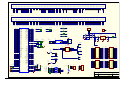
&38 %RDUG 'HVFULSWLRQ
This chapter provides detailed description of CPU board including
all DIP switches, jumpers and connectors.
CPU board can work standalone or in connection with the Mainboard. If the Mainboard is
in use, please switch all switches on CPU board configuration DIP to OFF.
&38 %2$5' 29(59,(:
CPU board is designed as low cost board, which provides compatibility on Interface Bus
and the Device Bus level for different CPUs. Additionally, headers pin compatible to CPU
pins are provided.
This part contains description of CPU board for MB90F543CPU.
Connectors
Jumpers, buttons and switches
Board layout
&211(&7256
. %XV ,QWHUIDFH FRQQHFWRU
This connector serves for connecting the CPU board to the Mainboard.
. 'HYLFH %XV FRQQHFWRU
This connector provides connection to CPU peripherals.
Note: For the pinout of these connectors, please see the attachments section of this
manual.
. &38 6HULDO LQWHUIDFH FRQQHFWRU
AD00 1
2 AD01
MD0 3
4 MD2
SERRES 5
6 SIN
SOT 7
8 SCK
VCC 9
10 GND
The serial interface connector should be used only when the CPU board is not connected
to the mainboard, because mainboard connects its own serial (RS232) interface to the
UART0 and UART1 CPU signals. To be able to use the K7 connector, please refer to the
description of J7, J8, J9 jumpers later in this section.
Warning: if you want to use the K7 connector when Mainboard is
connected to the CPU board, you have to disconnect the serial interface
selected by J7-J9 from the RS232 drivers on the Mainboard. To achieve this,
remove jumpers on positions 3-4, 5-6 from both the J21 and J22 headers on
the Mainboard. Also, when the Async. Serial programming mode is set on
the Mainboard System control DIP switches, the FPGA UART RS232 driver
is connected to UART0 or UART1 (depending on the setting of the
UART0/1 switch) after reset. If you want to use K7 also in that case, remove
the 3-4, 5-6 jumpers on the J23 as well.
. SRZHU VXSSO\ FRQQHFWRU
GND
+9V
Before applying the power to the Devkit16, check the polarity of your power chord plug –
the GND must be in the center, while the +9V on the shell of the connector. Even thought
the DevKit16 power lines are protected by a diode on the power input, do not ever apply
power with the opposite polarity. Also, make sure that the power supply complies to the
specifications in chapter CPU board Power Supply Requirements.
. . .
. &38 SLQV FRQQHFWRUV
.
.
A16 2 A17
INT6 31
32 INT7
A18 4 A19
ADTG 33
34 AVCC
A20 6 A21
AVR+ 35
36 AVR-
A22 8 A23
AVss 37
38 AN0
10 #RD
AN1 39
40 AN2
12 #WRL
AN3 41
42 Vss
#WRH 14 HRQ
AN4 43
44 AN5
#HAK 15
16 RDY
AN6 45
46 AN7
18 SOT0
TIN0 47
48 TOT0
SCK0 19
20 SIN0
MD0 49
50 MD1
SIN1 21
22 SCK1
FVCC 23
24 SOT1
SOT2 25
26 SCK2
SOT2 25
26 SIN2
INT4 25
26 INT5
ALE GND CLK 17
.
MD2 51
.
IN0 53
54 IN1
IN2 54
56 IN3
IN4 57
58 IN5
OUT2/IN6 59
VSS 81
X1 83
52 #HST
60 OUT3/IN7
82 X0
PPG0 61
62 PPG1
84 VCC
PPG2 63
64 PPG3
AD00 85
86 AD01
OUT0 65
66 OUT1
AD02 87
88 AD03
TIN1 67
68 TOT1
AD04 89
90 AD05
INT0 69
70 INT1
AD06 91
92 AD07
INT2 71
72 INT3
AD08 93
94 AD09
TX0 73
74 RX0
AD10 95
96 AD11
TX1 75
76 RX1
AD12 97
98 AD13
RST 77
78 PA0
AD14 99
100 AD15
X1A 79
80 X0A
- 9&& FRQQHFWRU
1: VCC
2: VCC
3: VCC
4: VCC
- *1' FRQQHFWRU
1: GND
2: GND
3: GND
4: GND
5: GND
6: GND
- 8 0 3 ( 5 6 % 8 7 7 2 1 6
$ 1 '
6 : , 7 & + ( 6
- 6XSSO\ IRU WKH ZKROH ERDUG
When SHORT, the +5V from the voltage regulator is connected to board VCC. This
jumper must be removed when using an external +5V power supply to avoid current
flowing back to the regulator.
- 6XSSO\ IRU &38
When SHORT, the VCC is connected to CPU’s VCC pins. Before removing this jumper,
remove the J3 (AVCC to CPU) jumper as well to completely disconnect the power from
the CPU.
- $QDORJ 6XSSO\ IRU &38
When SHORT, board’s VCC is connected to CPU’s AVcc pin.
- $QDORJ *URXQG IRU &38
When SHORT, board’s GND is connected to CPU’s AGND pin.
- $QDORJ 5HIHUHQFH 9ROWDJH IRU &38
When SHORT, board’s VCC is connected to CPU’s AVR+ pin. When removed, the
voltage at the AVR+ pin is set to 4V
- $QDORJ 5HIHUHQFH 9ROWDJH IRU &38
When SHORT, board’s GND is connected to CPU’s AVR- pin. When removed, the
voltage at the AVR- pin is set to 0.9V.
- - - 8$57 VHOHFWLRQ IRU WKH . FRQQHFWRU
These jumpers select, which of the two UART0, UART1 interfaces signals will be
connected to the pins of the K7 connector. If all of these jumpers are in
1-2 position - the UART1 interface signals will be connected to the K7
2-3 position – the UART0 interface signals will be connected to the K7 connector.
Default setting: the UART1 signals are connected to the K7.
Note: The J7 jumper selects between SCK1 and SCK0, J8 between SIN1 and SIN0
and J9 between SOT1 and SOT0
Warning: if you want to use the K7 connector when Mainboard is
connected to the CPU board, you have to disconnect the selected serial
interface (UART0 or UART1) from the RS232 drivers on the Mainboard. To
achieve this, remove jumpers on positions 3-4, 5-6 from both the J21 and J22
headers on the Mainboard. Also, when the Mainboard is connected to the
CPU board and the Async. Serial programming mode is set on the Mainboard
System control DIP switches, the FPGA UART is connected to UART0 or
UART1 (depending on the setting of the UART0/1 switch) after reset. If you
want to use K7 also in that case, remove the 3-4, 5-6 jumpers on the J23.
& VRIWZDUH HPXODWLRQ MXPSHUV
- - ,
These jumpers allow to use Mainboard’s I2C connector/EEPROM memory even in the
case, when CPU itself doesn’t provide the I2C interface. When both of these jumpers are
SHORT, the CPU’s HRQ signal is connected to the Mainboard’s SDA signal (via J19) and
#HAK signal is connected to SCL signal. An user can then program the #HAK, HRQ
signals to behave as I2C interface.
- - /RZ VSHHG ;7$/ MXPSHUV
When short, these jumpers connect the 32.768 kHz crystal to the Bus Interface connector
X1A, X0A pins.
- - +LJK VSHHG ;7$/ MXPSHUV
When short, these jumpers connect the 4MHz crystal to the Bus Interface connector X0,
X1 pins.
6: ² 5HVHW EXWWRQ
This button can be used for reseting the CPU.
6: ² +DUGZDUH VWDQGE\ EXWWRQ
While this button is pressed, the CPU stays in the standby mode (all oscillators are
stopped, all I/O pins are set to high impedance state, special purpose registers such as the
accumulator are reset to their default values, but content of internal RAM is preserved)
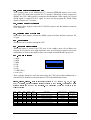
6: ² &38 ',3 VZLWFKHV
1: MD0
2: MD1
3: MD2
4: S-R
5: S-H
6: H-R
7: AD00 (P00)
8
7
6
5
4
3
2
1
ON
8: AD01 (P01)
These switches should be used only when using the CPU board without Mainboard, or
with the FPGA disabled (see the description of J29 in the Mainboard section).
0' 0' 0' ² WKHVH VZLWFKHV DUH FRQQHFWHG WR &38 SLQV 0' 0' 0' ,Q
WKH 21 SRVLWLRQ D VZLWFK SXOOV WKH VLJQDO FRQQHFWHG WR LW WR ORJ ¶· 7KH VHWWLQJ RI WKHVH
VZLWFKHV DIIHFWV WKH PRGH RI
WKH
SURFHVVRU
7KH
GHVFULSWLRQ
RI
DOO
WKH
PRGHV
LV
LQ WKH
IROORZLQJ WDEOH
MD2
MD1
MD0
ON
ON
ON
ON
OFF
OFF
OFF
OFF
ON
ON
OFF
OFF
ON
ON
OFF
OFF
ON
OFF
ON
OFF
ON
OFF
ON
OFF
AD00/
P00
OFF
OFF
OFF
OFF
X
X
ON
X
AD01
/P01
OFF
OFF
OFF
OFF
X
X
ON
X
Mode name
Reset vector area
External vector mode 0
External vector mode 1
External vector mode 2
Internal vector mode
Reserved
Reserved
Async serial programming
Reserved
External
External
External
Internal
External data
bus witdth
8
16
16
(Mode data)
4: S-R – if ON, this switch connects the RES pin of the K7 connector to the CPU’s #RST
signal.
5: S-H – if ON, this switch connects the RES pin of the K7 connector to the CPU’s #HST
signal.
6. H-R – if ON, the #RST and #HST signals are connected together.
7: AD00, 8:AD01 – if ON, the AD00/P00 and AD01/P01 signals are pulled to log. ‘0’
level. This setting must be done for bringing processor to the Serial programming mode.
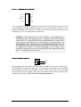
8 7 6 5
4 3
2 1
ON
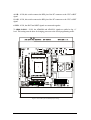
Figure 1: CPU board layout and default jumper settings
'()$8/7 +: 6(77,1*6
These jumpers come in the SHORT position as a default factory setting:
J2: The CPU is connected to the +5V power supply through this jumper
J3: The CPU AVCC supply pin is connected +5V power supply through this jumper
J4: The CPU AGND supply pin is connected to the GND through this jumper
J5: The CPU AVR+ pin is connected to the +5V voltage through this jumper
J6: The CPU AVR- pin is connected to the 0V voltage through this jumper
J7-9: The CPU UART1 signals are connected to the K7 connector
J13: The board is powered from the +5V from the power supply voltage regulator
J19: The CPU HRQ pin is connected to the SDA Mainboard signal
J20: The CPU #HAK pin is connected to the SCL Mainboard signal
&KDSWHU
&38 %RDUG 3RZHU 6XSSO\
5HTXLUHPHQWV
CPU board does not come with power supply, please check, if your
power supply match the requirements before you plug it to the CPU
board!
Power supply voltage: 9V
Power supply current (CPU board MB90F543 with Main board connected):
Single chip CPU mode, no external peripheral connected: 290mA max.
External bus mode, no peripheral connected: 350mA
External bus with:
: (
keyboard connected: 450mA typical, but can vary with the keyboard used
(most of modern AT keyboard uses max. 100mA. User should check his
keyboard current requirements before connecting the keyboard to the
DevKit16 Mainboard).
keyboard and VGA interface connected: 650mA
5 ( & 2 0 0 ( 1 '
$
1 2 7
0 , 1 ' ( / , 9 ( 5
$ % 2 9 ( % 2 $ 5 '
6 8 3 3 / <
7 + (
: , / /
8 6 , 1 *
2 8 7 3 8 7
9
& 8 5 5 ( 1 7 6
' ( 9 . , 7 % (
6 7 $ % , / , = ( '
& 8 5 5 ( 1 7 $ 6
: , / /
, )
7 + (
6 3 ( & , ) , ( '
1 2 7
3 ( 5 , 2 ' , & $ / / <
6 8 3 3 / <
: , 7 +
6 8 3 3 / <
& $ 1
, 1
: 2 5 .
5 ( 6 ( 7
3 2 : ( 5
3 2 : ( 5
7 + (
6 3 ( & , ) , & $ 7 , 2 1
3 5 2 3 ( 5 / <
% <
7 + (
²
7 + (
0 % 3 2 : ( 5
6 8 3 ( 5 9 , 6 2 5 Warning: If the DevKit16 is powered using the on-board stabilizer, the
supply current must not exceed the 1A limit of the stabilizer. Before
connecting any peripheral to the DevKit16, please check that its power
supply current requirements doesn’t does not cause this limit to be exceeded.
&KDSWHU
:DUUDQW\ DQG 'LVFODLPHU
To the maximum extent permitted by applicable law, Fujitsu Microelectronics Europe GmbH
restricts its warranties and its liability for the DEVKIT16 and all its deliverables (eg. software,
application examples, target boards, evaluation boards, etc.), its performance and any consequential
damages, on the use of the Product in accordance with (i) the terms of the License Agreement and the
Sale and Purchase Agreement under which agreements the Product has been delivered, (ii) the
technical descriptions and (iii) all accompanying written materials. In addition, to the maximum extent
permitted by applicable law, Fujitsu Microelectronics Europe GmbH disclaims all warranties and
liabilities for the performance of the Product and any consequential damages in cases of unauthorised
decompiling and/or reverse engineering and/or disassembling. Note, the DEVKIT16 and all its
deliverables are intended and must only be used in an evaluation laboratory environment.
1. Fujitsu Microelectronics Europe GmbH warrants that the Product will perform substantially in
accordance with the accompanying written materials for a period of 90 days form the date of receipt
by the customer. Concerning the hardware components of the Product, Fujitsu Microelectronics
Europe GmbH warrants that the Product will be free from defects in material and workmanship
under use and service as specified in the accompanying written materials for a duration of 1 year
from the date of receipt by the customer.
2. Should a Product turn out to be defect, Fujitsu Microelectronics Europe GmbH´s entire liability and
the customer´s exclusive remedy shall be, at Fujitsu Microelectronics Europe GmbH´s sole
discretion, either return of the purchase price and the license fee, or replacement of the Product or
parts thereof, if the Product is returned to Fujitsu Microelectronics Europe GmbH in original
packing and without further defects resulting from the customer´s use or the transport. However,
this warranty is excluded if the defect has resulted from an accident not attributable to Fujitsu
Microelectronics Europe GmbH, or abuse or misapplication attributable to the customer or any
other third party not relating to Fujitsu Microelectronics Europe GmbH.
3. To the maximum extent permitted by applicable law Fujitsu Microelectronics Europe GmbH
disclaims all other warranties, whether expressed or implied, in particular, but not limited to,
warranties of merchantability and fitness for a particular purpose for which the Product is not
designated.
4. To the maximum extent permitted by applicable law, Fujitsu Microelectronics Europe GmbH´s and
its suppliers´ liability is restricted to intention and gross negligence.
NO LIABILITY FOR CONSEQUENTIAL DAMAGES
To the maximum extent permitted by applicable law, in no event shall Fujitsu
Microelectronics Europe GmbH and its suppliers be liable for any damages whatsoever
(including but without limitation, consequential and/or indirect damages for personal injury,
assets of substantial value, loss of profits, interruption of business operation, loss of information,
or any other monetary or pecuniary loss) arising from the use of the Product.
Should one of the above stipulations be or become invalid and/or unenforceable, the remaining
stipulations shall stay in full effect.
&KDSWHU
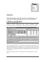
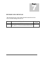
5HYLVLRQ DQG (UURU /LVW
The following bugs have been found with the board and need to be
observed when working with this tool:
Date
Revisions - Errors
05.11.1999
13.02.2000
Version 1.2 is valid for CPU Board ver. 1.3
The table “Device Bus (K2) and Interface Bus (K1 ) connectors
pins” (pages 16, 17, 18) was not consistent with the schematics.
Table1: List of found errors and revisions for version V1.2
Revised
Version
V1.2
V1.21
&KDSWHU
$SSHQGL[
Here you will find Interface bus and Device Bus description and CPU
board schematics.
'HYLFH %XV . DQG ,QWHUIDFH %XV . FRQQHFWRUV SLQV
DIN Conn.
PIN
PIN NO.
Device Bus
Interface Bus
CPU Pin Nr.
Function
CPU PIN Nr.
SIGNAL
2nd Function
A1
18
SOT0
85
AD00
P00
B1
19
SCK0
86
AD01
P01
C1
20
SIN0
87
AD02
P02
A2
24
SOT1
88
AD03
P03
B2
22
SCK1
89
AD04
P04
C2
21
SIN1
90
AD05
P05
A3
91
AD06
P06
B3
92
AD07
P07
C3
93
AD08
P10
A4
69
INT0
94
AD09
P11
B4
70
INT1
95
AD10
P12
C4
71
INT2
96
AD11
P13
A5
72
INT3
97
AD12
P14
B5
29
INT4
98
AD13
P15
C5
30
INT5
99
AD14
P16
A6
31
INT6
100
AD15
P17
B6
32
INT7
1
A16
P20
C6
25
SOT2
2
A17
P21
A7
26
SCK2
3
A18
P22
B7
28
SIN2
4
A19
P23
C7
5
A20
P24
A8
6
A21
P25
B8
7
A22
P26
C8
8
A23
P27
A9
9
ALE
P30
B9
10
\RD
P31
C9
12
\WRL
P32
A10
13
\WRH
P33
B10
14
HRQ
P34
DIN Conn.
PIN
PIN NO.
Device Bus
Interface Bus
CPU Pin Nr.
Function
A11
47
TIN0
B11
48
TOT0
C10
C11
CPU PIN Nr.
SIGNAL
2nd Function
15
\HAK
P35
16
RDY
P36
17
CLK
P37
GND
GND
GND
A12
67
TIN1
18
SOT0
P40
B12
68
TOT1
19
SCK0
P41
C12
20
SIN0
P42
A13
24
SOT1
P45
B13
53
IN0
22
SCK1
P44
C13
54
IN1
21
SIN1
P43
A14
55
IN2
25
SOT2
P46
B14
56
IN3
26
SCK2
P47
C14
57
IN4
28
SIN2
P50
A15
58
IN5
B15
59
OUT2/IN6
C15
60
OUT3/IN7
61
PPG0
P80
A16
65
OUT0
62
PPG1
P81
B16
66
OUT1
67
TIN1
P86
C16
SDA
SCL
VCC
VCC
A17
59
OUT3/IN7
33
ADTG
P55
C17
60
OUT2/IN6
AVCC
68
TOT1
P87
34
AVCC
A18
35
AVR+
B18
36
AVR-
37
AGND
38
AN0
C17
C18
AGND
A19
B19
39
C19
GND
P60
AN1
P61
GND
GND
C20
40
AN2
P62
A21
41
AN3
P63
C20
43
AN4
P64
A21
44
AN5
P65
B21
45
AN6
P66
46
AN7
P67
77
\RST
C21
A22
61
PPG0
B22
62
PPG1
52
\HST
C22
63
PPG2
69
INT0
P90
A23
64
PPG3
70
INT1
P91
B23
71
INT2
P92
C23
72
INT3
P93
A24
73
TX0
29
INT4
P51
B24
74
RX0
30
INT5
P52
C24
75
TX1
31
INT6
P53
A25
76
RX1
32
INT7
P54
B25
53
IN0
P70
C25
54
IN1
P71
A26
55
IN2
P72
B26
56
IN3
P73
C26
59
OUT2/IN6
P76
A27
60
OUT3/IN7
P77
B27
NC(SGO)
C27
NC(SGA)
DIN Conn.
PIN
PIN NO.
Device Bus
CPU Pin Nr.
Interface Bus
Function
CPU PIN Nr.
SIGNAL
2nd Function
A28
73
TX0
P94
B28
74
RX0
P95
C28
75
TX1
P96
A29
76
RX1
P97
B29
79
X1AJ
C29
80
X0AJ
A30
82
X0J
B30
83
C30
VCC
X1J
VCC
A31
49
MD0
B31
50
MD1
51
MD2
C31
NC
A32
B32
C32
NC
GND
GND
A32
B32
C32
GND
A31
B31
C31
A30
B30
C30
A29
B29
C29
A28
B28
C28
A27
B27
C27
A26
B26
C26
A25
B25
C25
VCC
TX0
RX0
TX1
RX1
A24
B24
C24
A23
B23
C23
P P G3
A22
B22
C22
P P G0
P P G1
P P G2
A21
B21
C21
A20
B20
C20
GND
AGND
A19
B19
C19
A18
B18
C18
A17
B17
C17
OUT3/IN7
OUT2/IN6
AVCC
OUT0
OUT1
VCC
A16
B16
C16
A15
B15
C15
IN5
OUT2/IN6
OUT3/IN7
A14
B14
C14
IN2
IN3
IN4
A13
B13
C13
A12
B12
C12
IN0
IN1
TIN0
TOT0
GND
TIN1
TOT1
A11
B11
C11
A10
B10
C10
A9
B9
C9
A8
B8
C8
A7
B7
C7
SCK2
SIN2
A6
B6
C6
INT6
INT7
SOT2
A5
B5
C5
INT3
INT4
INT5
INT0
INT1
INT2
A4
B4
C4
A3
B3
C3
A2
B2
C2
SOT1
SCK1
SIN1
SOT0
SCK0
SIN0
A1
B1
C1
K2
DIN_41612
#RST
77
PA0
78
49
50
51
#HST
X1
22pF 4MHz
X1
52
83
X0
82
X1A
79
X0A
80
P90/INT0
P91/INT1
P92/INT2
P93/INT3
P94/TX0
P95/RX0
P96/TX1
P97/RX1
#RST
PA0
MD0
MD1
MD2
AVss
P60/AN0
P61/AN1
P62/AN2
P63/AN3
P64/AN4
P65/AN5
P66/AN6
P67/AN7
P70/IN0
P71/IN1
P72/IN2
P73/IN3
P74/IN4
P75/IN5
P76/OUT2/IN6
P77/OUT3/IN7
P80/PPG0
P81/PPG1
P82/PPG2
P83/PPG3
P84/OUT0
P85/OUT1
P86/TIN1
P87/TOT1
C
X1
VCC
VCC
36
AVR-
37
AGND
38
39
40
41
43
44
45
46
AN0
AN1
AN2
AN3
AN4
AN5
AN6
AN7
53
54
55
56
57
58
59
60
IN0
IN1
IN2
IN3
IN4
IN5
OUT2/IN6
OUT3/IN7
X2
GND
C9
C8
22pF
22pF
32.768KHz
X0A
MB90540
61
62
63
64
65
66
67
68
PPG0
PPG1
PPG2
PPG3
OUT0
OUT1
TIN1
TOT1
27
C
VSS
VSS
VSS
R1
220R
R2
1K
C10
10M/25V
CT
VSC
OUTC
GND
RESET
VSA
VSB/RESIN
VCC
8
7
6
5
#RST
1N4007 SMD
D7
A
K
1N4007 SMD
1N4007 SMD
GND PL1
GND
A32
B32
C32
MD2
GND
OUT
OUT
VCC
C15
100N
GND
GND
GND
PWRD
SIN0
SERRES
A
AD00
MD0
D2
K
1N4148 SMD
1
3
5
7
9
K3
AD01
MD2
2
4
6
8
10
J9
JUMPER3
SCK1
1
GND
GND
C12
100N
J7
JUMPER3
SOT1
1
A16
A18
A20
A22
ALE
GND
#WRH
#HAK
CLK
SCK0
SIN1
FVCC
SOT2
C
INT4
1
3
5
7
9
11
13
15
17
19
21
23
25
27
29
#HST
SW2
PB1720
GND
VCC
J11
VCC
1
10K
10K
10K
10K
10K
GND
R13 10K
R14 10K
R6
1K
SW3
VCC
R8
R9
R10
R11
R12
MD0
MD1
MD2
#RST
#HST
#HST
AD00
AD01
1
2
3
4
5
6
7
8
16
15
14
13
12
11
10
9
SW DIP-8
A17
A19
A21
A23
#RD
#WRL
HRQ
RDY
SOT0
SIN0
SCK1
SOT1
SCK2
SIN2
INT5
MD2
IN0
IN2
IN4
OUT2/IN6
PPG0
PPG2
OUT0
TIN1
INT0
INT2
TX0
TX1
#RST
X1A
INT7
AVCC
AVRAN0
AN2
GND
AN5
AN7
TOT0
MD1
GND
X1
AD00
AD02
AD04
AD06
AD08
AD10
AD12
AD14
1
3
5
7
9
11
13
15
17
19
21
23
25
27
29
J10
1
2
3
4
5
6
1
2
3
4
HEADER 4
GND
SERRES
#RST
D3
LED 5mm
INT6
ADTG
AVR+
AGND
AN1
AN3
AN4
AN6
TIN0
MD0
1
3
5
7
9
11
13
15
17
19
GND
K6
2
4
6
8
10
12
14
16
18
20
1
3
5
7
9
11
13
15
17
19
HEADER 10X2
X0
FVCC
AD01
AD03
AD05
AD07
AD09
AD11
AD13
AD15
2
4
6
8
10
12
14
16
18
20
HEADER 10X2
HEADER 6
Title
GND
Size
A3
Date:
File:
#HST
IN1
IN3
IN5
OUT3/IN7
PPG1
PPG3
OUT1
TOT1
INT1
INT3
RX0
RX1
PA0
X0A
2
4
6
8
10
12
14
16
18
20
22
24
26
28
30
HEADER 15X2
K4
GND
VCC
K5
2
4
6
8
10
12
14
16
18
20
22
24
26
28
30
HEADER 15X2
SOT0
C13
100N
C5
10M/25V
A31
B31
C31
C18
100M/25V
1
SCK0
C3
100N
IN
C16
100N
JUMPER3
SIN1
GND
#RST
C4
100N
MD0
MD1
X0J
X1J
VCC
IN
2
+5V
J13
JUMPER2
IC3
LM7805
K7
BOXHEADER 5X2
J4
JUMPER2
J2
JUMPER2
2
GND
J8
MB3771
VCC
C1
10M/25V
C2
100N
A30
B30
C30
A29
B29
C29
RX1
X1AJ
X0AJ
A28
B28
C28
A
+5V
PL3
1 2
+5V
K
GND
K
D6
1N4007 SMD
D5
K
GND 1
R16
3K6
R4
220R
SW1
PB1720
GND
TX0
RX0
TX1
A27
B27
C27
OUT3/IN7
SGO
SGA
A26
B26
C26
IN2
IN3
OUT2/IN6
A25
B25
C25
INT7
IN0
IN1
A24
B24
C24
INT4
INT5
INT6
A23
B23
C23
INT1
INT2
INT3
A22
B22
C22
#RST
#HST
INT0
A21
B21
C21
AN5
AN6
AN7
AN2
AN3
AN4
A20
B20
C20
A19
B19
C19
1
1
IC2
1
2
3
4
VCC
R3
1K
J6
JUMPER2
GND
FVCC
11
42
81
A
C11
100N
R15
10K
D4
GND
1
K
X1A
J3
JUMPER2
1
22pF
GND
J5
JUMPER2
GND
23
84
1
2
AVR+
1
35
X1J
VCC
GND
AVR-
#HST
XO
AVCC
A
A
69
70
71
72
73
74
75
76
AVR+
34
PL2
1
X0J
K
INT0
INT1
INT2
INT3
TX0
RX0
TX1
RX1
P30/ALE
P31/#RD
P32/#WRL/#WR
P33/#WRH
P34/HRQ
P35/#HAK
P36/RDY
P37/CLK
AVcc
2
1
SK 129 25.4mm
J18
JUMPER2
X1
CH1
X1AJ
J17
JUMPER2
X0
1
9
10
12
13
14
15
16
17
MD0
MD1
MD2
GND
C6
ALE
#RD
#WRL
#WRH
HRQ
#HAK
RDY
CLK
P20/A16
P21/A17
P22/A18
P23/A19
P24/A20
P25/A21
P26/A22
P27/A23
J16
JUMPER2
X1A
#HAK
D1
1N4148 SMD
C7
GND
1
2
3
4
5
6
7
8
P50/SIN2
P51/INT4
P52/INT5
P53/INT6
P54/INT7
P55/ADTG
P56/TIN0
P57/TOT0
SIN2
INT4
INT5
INT6
INT7
ADTG
TIN0
TOT0
SCL
HRQ
A AVCC
A16
A17
A18
A19
A20
A21
A22
A23
P10/AD08
P11/AD09
P12/AD10
P13/AD11
P14/AD12
P15/AD13
P16/AD14
P17/AD15
28
29
30
31
32
33
47
48
SDA
K9
K375A
X0AJ
1
93
94
95
96
97
98
99
100
P40/SOT0
P41/SCK0
P42/SIN0
P43/SIN1
P44/SCK1
P45/SOT1
P46/SOT2
P47/SCK2
SOT0
SCK0
SIN0
SIN1
SCK1
SOT1
SOT2
SCK2
1
AD08
AD09
AD10
AD11
AD12
AD13
AD14
AD15
P00/AD00
P01/AD01
P02/AD02
P03/AD03
P04/AD04
P05/AD05
P06/AD06
P07/AD07
18
19
20
21
22
24
25
26
1
85
86
87
88
89
90
91
92
1
AD00
AD01
AD02
AD03
AD04
AD05
AD06
AD07
J15
JUMPER2
X0A
J20
JUMPER2
1
SOUND
J19
JUMPER2
IC1
AN0
AN1
GND
A18
B18
C18
AVR+
AVRAGND
A17
B17
C17
ADTG
TOT1
AVCC
A16
B16
C16
P P G1
TIN1
VCC
A15
B15
C15
SDA
SCL
P P G0
A14
B14
C14
SOT2
SCK2
SIN2
A13
B13
C13
A12
B12
C12
SOT1
SCK1
SIN1
RDY
CLK
GND
SOT0
SCK0
SIN0
A11
B11
C11
A10
B10
C10
#WRH
HRQ
#HAK
A9
B9
C9
ALE
#RD
#WRL
A8
B8
C8
A21
A22
A23
A7
B7
C7
A18
A19
A20
A6
B6
C6
AD15
A16
A17
A5
B5
C5
AD12
AD13
AD14
A4
B4
C4
AD09
AD10
AD11
A3
B3
C3
AD06
AD07
AD08
A2
B2
C2
AD03
AD04
AD05
AD00
AD01
AD02
A1
B1
C1
K1
DIN_41612
Devkit16 - CPU Board
Number
Revision
Ver. 1
8-Dec-1999
D:\Cpuboard13.ddb
3
Sheet of
Drawn By: