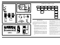
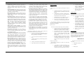
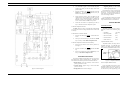
1
LBI-31629B Maintenance Manual M-PD SYSTEM 136-174 MHz PERSONAL TWO-WAY FM RADIO COMBINATION INCLUDES SERVICE SECTION . . . . . . . . . . . . . . LBI-31677 ericssonz Ericsson Inc. Private Radio Systems Mountain View Road Lynchburg, Virginia 24502 1-800-528-7711 (Outside USA, 804-528-7711) Printed in U.S.A. LBI-31629 SPECIFICATIONS TABLE OF CONTENTS Page SPECIFICATIONS . . . . . . . . . . . . . . . . . . . . . . . . . . . . . . . . . . . . . . . . . . . . . . . . . . . . 1 OPTIONS AND ACCESSORIES . . . . . . . . . . . . . . . . . . . . . . . . . . . . . . . . . . . . . . . . . . . . . 2 COMBINATION NOMENCLATURE . . . . . . . . . . . . . . . . . . . . . . . . . . . . . . . . . . . . . . . . . . 2 DESCRIPTION . . . . . . . . . . . . . . . . . . . . . . . . . . . . . . . . . . . . . . . . . . . . . . . . . . . . . . 2 OPERATION . . . . . . . . . . . . . . . . . . . . . . . . . . . . . . . . . . . . . . . . . . . . . . . . . . . . . . . 3 SYSTEM ANALYSIS . . . . . . . . . . . . . . . . . . . . . . . . . . . . . . . . . . . . . . . . . . . . . . . . . . . 4 MAINTENANCE . . . . . . . . . . . . . . . . . . . . . . . . . . . . . . . . . . . . . . . . . . . . . . . . . . . . . 9 INTRINSICALLY SAFE USAGE . . . . . . . . . . . . . . . . . . . . BATTERIES . . . . . . . . . . . . . . . . . . . . . . . . . . . . . ACCESSORIES . . . . . . . . . . . . . . . . . . . . . . . . . . . MEMORY EFFECT IN NICKEL-CADMIUM BATTERIES: . . . REDUCED CAPACITY IN NICKEL- CADMIUM BATTERIES: . . . . . . . . . . . . . . . . . . . . . . . . . . . . . . . . . . . . . . . . . . . . . . . . . . . . . . . . . . . . . . . . . . . . . . . . . . . . . . . . . . . . . . . . . . . . . . . . . . . . . . . . . . . . . . . . . . . . 12 . 12 . 12 . 12 . 13 INTERCONNECTION DIAGRAMS . . . . . . . . . . . . . . . . . . . . . . . . . . . . . . . . . . . . . . . . . . . 14 OUTLINE DIAGRAMS: Radio Board . . . . Controller Board . . Signaling Board . . LCD Board . . . . . Battery Packs . . . . . . . . . . . . . . . . . . . . . . . . . . . . . . . . . . . . . . . . . . . . . . . . . . . . . . . . . . . . . . . . . . . . . . . . . . . . . . . . . . . . . . . . . . . . . . . . . . . . . . . . . . . . . . . . . . . . . . . . . . . . . . . . . . . . . . . . . . . . . . . . . . . . . . . . . . . . . . . . . . . . . . . . . . . . . . . . . . . . . . . . . . . . . . . . . . . . . . . . . . . . . . . . . . . . . . . . . . . . . . . . . . . . . . . . . . . . . . . . . . . . . . . . 15 17 19 20 22 SCHEMATIC DIAGRAMS: Radio Board . . . . . . Controller Board . . . . Signaling Board . . . . LCD Board . . . . . . . Battery Packs . . . . . . . . . . . . . . . . . . . . . . . . . . . . . . . . . . . . . . . . . . . . . . . . . . . . . . . . . . . . . . . . . . . . . . . . . . . . . . . . . . . . . . . . . . . . . . . . . . . . . . . . . . . . . . . . . . . . . . . . . . . . . . . . . . . . . . . . . . . . . . . . . . . . . . . . . . . . . . . . . . . . . . . . . . . . . . . . . . . . . . . . . . . . . . . . . . . . . . . . . . . . . . . . . . . . . . . . . . . . . . . . . . . . . . . . . . . . . . . . 16 18 19 21 22 MECHANICAL PARTS BREAKDOWN . . . . . . . . . . . . . . . . . . . . . . . . . . . . . . . . . . . . . . . . 23 PARTS LISTS: M-PD Radio Chassis . Mechanical Parts . . . Radio Board . . . . . Controller Board . . . Signaling Board . . . LCD Board . . . . . . 13 24 25 26 27 27 . . . . . . . . . . . . . . . . . . . . . . . . . . . . . . . . . . . . . . . . . . . . . . . . . . . . . . . . . . . . . . . . . . . . . . . . . . . . . . . . . . . . . . . . . . . . . . . . . . . . . . . . . . . . . . . . . . . . . . . . . . . . . . . . . . . . . . . . . . . . . . . . . . . . . . . . . . . . . . . . . . . . . . . . . . . . . . . . . . . . . . . . . . . . . . . . . . . . . . . . . . . . . . . . . . . . . . . . . . . . . . . . . . . . . . . . . . . . . . . . . . . . . . . . . . . . . . . . . . . . . . . . . . . . . . . . . . . . . . . . . . . . . . . . SYSTEM Frequency Range 136 MHz to 160 MHz 150 MHz to 174 MHz Frequency Stability Battery Drain (at 7.5 VDC) Standby Receiver (Rated Audio) Transmitter Dimensions (H x W x D) (With Standard Capacity) (With High Capacity (short) Battery) (With High Capacity (long) Battery) (With Extra High Capacity Battery) Weight (With Standard Capacity Battery) (With High Capacity (short) Battery) (With High Capacity (long) Battery) (With Extra High Capacity Battery) Operable Temperature Range TRANSMIT RF Power Output Spurious Emissions Maximum Deviation FM Hum & Noise (EIA) Audio Distortion (60% MOD) Frequency Stability (-30°C to + 60°C) RF Load Impedance Microphone Sensitivity (EIA 60% MOD) Maximum Attack Time (PTT Pushed) Audio Frequency Response RECEIVE Sensitivity (12 dB SINAD) Spurious Emissions Spurious Response Rejection IM Distortion Rejection Adjacent Channel Selectivity Squelch Sensitivity Distortion (EIA 0.5 Watt) Audio Frequency Response FCC Identification Number AXA9WNTR-145-A AXA9WNTR-145-B 5 PPM 65 Milliamperes 195 Milliamperes 1.9 amperes 183 x 69 x 43 mm 183 x 69 x 43 mm 219 x 69 x 43 mm 219 x 69 x 43 mm 24 ounces 24 ounces 29 ounces 29 ounces -30°C to +60°C 0.5 to 5 Watts -37 dBm 5 kHz -45 dB 3% 5 PPM 50 ohms Less than 90 dB SPL 25 milliseconds Within +1 and -3 dB of a 6 dB/octave pre-emphasis from 300 Hz to 3000 Hz. -116 dBm -57 dBm 72 dB (Minimum) 70 dB (Minimum) 70 dB (30 kHz) 6 dB SINAD (Minimum) Adjustable 5% (Maximum) Within +1 and -3 dB of a 6 dB/octave de-emphasis from 300 Hz to 3000 Hz. Copyright © April 1987, General Electric Company 1 LBI-31629 COMBINATION NOMENCLATURE HB UHF Digits 1 & 2 Digit 3 Digit 4 Digit 5 Digit 6 Digit 7 Product Code Frequency Range Controller Selectivity Stability Power Souce 800 MHz BELT CLIP PDHC15 PD SWIVEL MOUNT PDHC16 CARRYING CASES WITH BELT LOOP PDHC11 PDHC12 WITH SWIVEL MT PDHC13 PDHC14 STANDARD MODEL SCAN MODEL SHOULDER STRAP PDHC18 G C S 5 M 136-160 MHz System Standard 5 PPM HIGH CAP. NICD H N 150-174 MHz STD CAP. NICD SYSTEM MODEL P OR HEADSET/MIC OR GENERAL ELECTRIC EARPIECE PDAB10 PDAC10 SPKR-MIC PDAE-10 bdac bdac bdac bdac bdac bdac bdac bdac bdac bdac bdac bdac bdac bdac bdac bdac bdac bdac bdac bdac bdac bdac bdac bdac bdac bdac bdac bdac bdac bdac bdac bdac bdac bdac bdac bdac bdac bdac bdac bdac bdac bdac bdac bdac bdac bdac bdac bdac bdac bdac bdac bdac bdac bdac bdac bdac bdac bdac bdac bdac bdac bdac bdac bdac bdac bdac bdac bdac bdac bdac bdac bdac bdac bdac bdac bdac bdac bdac bdac GENERAL bdac bdac bdac bdac ELECTRIC bdac bdac bdac bdac bdac bdac bdac bdac bdac bdac bdac bdac bdac bdac bdac bdac bdac bdac bdac bdac bdac bdac bdac bdac bdac bdac bdac bdac bdac bdac bdac bdac bdac bdac bdac bdac bdac bdac bdac bdac bdac bdac bdac bdac bdac bdac bdac bdac bdac bdac bdac bdac bdac bdac bdac bdac bdac bdac bdac bdac GENERAL ELECTRIC GENERAL X HIGH CAP. NICD ELECTRIC PDPA10 (Optional) DESCRIPTION HIGH CAPACITY BATTERY Ericsson GE’s M-PD System Personal Radio is a highquality, high-performance, two-way, FM, communications unit consisting of a transmit/receive circuit with a frequency synthesizer controlled by a microprocessor. The M-PD Personal Radio is ideal for use in public services by providing the following features: (Standard) TOP VIEW TOP VIEW FRONT VIEW FRONT VIEW GENERAL MULTI-CHARGER H2A2L2A H2A2J1A H2A2M2A H2A2N1A 2 No Battery GE-STAR LANYARD PDAC12 INTERFACE CONNECTOR (Provided with PDAB10) STANDARD CAPACITY X 121 VAC 16 HR 121 VAC 1 HR 240 VAC 16 HR 240 VAC 1 HR ELECTRIC DESK CHARGER H2A1L2A H2A1J1A H2A1M2A H2A1N1A 121 VAC 16 HR 121 VAC 1 HR 240 VAC 16 HR 240 VAC 1 HR VEHICULAR CHGR/RPTR H2V01 - Vehicular Charger H2V02 - Vehicular Chgr/Rptr Control The same channel is used with and without Channel Guard by programming two different radio channels with the same frequency information but only one with Channel Guard capability. • Programmable Multi-Code Digital Channel Guard Encode/Decode: Similar capability as with Tone Channel Guard is provided. • 48 Channel Capability: Channel designation can be a mixture of numerics (0 - 48) and alphanumerics through the eight characters in the LCD display. Channel control can come from either the up/down channel ramping buttons, front keypad entry or the "Home" Channel feature. • Programmable Carrier Control Timer: Personality information includes an optional period of transmit time from 15 to 120 seconds, after which the unit will automatically unkey and provide an alerting tone. This feature is reinitiated on every PTT and the alert tone is removed upon release of the PTT. • Eight Programmable Modes: Up to eight modes are programmable with any number of channels in each mode: the sum of channels and blank channels in all modes equal to 48. • Minimum Volume Level: Personality information includes a minimum volume level below which the radio controls cease to reduce the volume. • Programmable Multi-Tone Channel Guard (CTCSS) Encode/Decode: Channel Guard tone frequencies within the range of 67 Hz to 210.7 Hz, including all of the standard EIA frequencies, may be programmed. Different encode/decode, encode only and with/without Channel Guard frequencies are also programmable into the radio. • Squelch Tail Elimination: Squelch and audio circuits are designed so that annoying squelch pops which may occur at the end of received messages are minimized, both with and without Channel Guard. This system is compatible with an existing GE system. • Programmable Squelch: The noise squelch opening threshold can be programmed for each channel. LBI-31629 • Channel Busy Lock Out: Personality information includes the capability to prevent the transmitter from operating on a channel where carrier activity is present. The "Channel Busy" indicator (BSY) is active during this time. • Automatic/Manual Power Levels: The desired power level on each channel can be programmed into the radio personality such that it is automatically selected channelby-channel or selected manually. • Home Channel Feature: A "Home" channel can be programmed into the radio which is selected by pressing the "Home" button. This allows a user to quickly reach a reference channel. Compatibility with Channel Guard, Digital Channel Guard, GE-STAR, DTMF, Dual Priority and Scan are maintained. Various audible alerting signals are available on choice when programming the radio. • DTMF Encode Reperatory Dialing: When enabled by the information programmed into the personality of the radio, the DTMF encode function can be used by either manually dialing from the keypad or by recalling a complete number stored in memory. Ten stored numbers, including the 1ast number dialed, up to 16 digits are easily recalled to the display for viewing. A convenient display overflow and shift mechanism is incorporated into the display control procedure. • Surveillance Feature: In addition to the ability to program the display 1ighting on or off per channel, the sidetone beep related to the operation of a radio control is capable of being disabled on a channel by channel basis. It is not necessary to press the PTT switch while dialing. Features needed for overdialing, autopatch and paging terminals, including programmed delays, pauses and the generation of the "*" and "#" DTMF pairs are included. • Eight Character Alphanumeric Liquid Crystal Display: This display is used to exhibit the condition of the radio. It shows: Channel Designation, Signaling ON/OFF, Transmit, Volume Level, Battery Condition, Channel Busy, High/Low Power output, SCAN 0N/0FF and Priority 1 & 2. • Programmable Dual-Priority Scan: The radio is programmed to listen to a selected channel while scanning back to two priority channels. The radio reverts to the priority 1evel channels should any activity occur on those channels. There are two 1evels of priority. The first priority channel takes precedence over the second priority channel and the second priority channel takes precedence over the user selected channel. • Simple Remote Control Capability: By connection through the UDC (Universal Devices Connector) a simple speaker/ microphone can be operated which can also control PTT and Volume level. • Push Button Controls Only: All control functions on the radio, with the exception of the power ON/OFF switch, are operated through push button controls on the top and sides of the radio. • Programmable through UDC: The entire personality of the radio is programmed into the radio through the UDC through four connections. The Ericsson GE TQ2310 Universal programmer is one method of programming the radio, while the capability exists to interface to an RS-232 device at a maximum of 1200 baud. • Keyboard Enable: Pressing two keypad keys (Secondary Function and KEY BD) in sequence activates the front DTMF keyboard. The user can then change radio functions as required. The top keypad is not protected in this manner for ease of using the frequently switched functions (volume, channel, Signaling On/Off, . . .etc.). • Two-Tone Sequential Encode/Decode: Selective calling encode, decode or encode/decode is enabled or disabled on each individual channel. Three simultaneous unique decodes are available for each channel to allow large systems the capability for individual and group calls. • Manual High/Low Power Selection: If programmed into the radio, the user will be able to manually select either high or low RF power output through the front panel keyboard. Physically an M-PD radio consists of three printed wire board assemblies and a battery pack as follows: a. A printed wire board specially shielded with zinc alloy on which the radio assembly (transmit/receive/synthesizer) is assembled. b. A Logic control board containing the microprocessor. c. A Display board carrying various display and indicating circuits. d. A battery pack that fits the M-PD main unit. e. Light weight metal front and back housing. Radio Assembly b. VCTCXO Module: The VCTCXO is a temperature compensated crystal oscillator to provide a 13.2 MHz reference frequency and has modulation capability. c. Phase Lock Loop: Consists of a frequency divider and a low current drain C-MOS IC for phase comparison. Transmit: The transmit circuit is made up of four major circuits as follows: a. Wideband Hybrid Exciter: Amplifies the signal from the frequency synthesizer with about 21 dB gain. b. Wideband Power Amplifier: Amplifies the output signal of the exciter (13 dB to 18 dB) to the desired output level for transmission. c. Wideband Power Control Hybrid IC: Can reduce the transmitter output level by 10 dB. d. Output Low pass Filter (LPF): Consists of a three stage LPF to eliminate higher harmonics. Logic Circuit The Logic circuit consists of a LCD board, a signaling board and a control board with an audio IC as follows: The transmitter completely covers the band within the split with no adjustments except for the RF power control voltage from the controller. a. LCD Board: Includes LCD driver circuits for the display. b. Signaling Board: Includes a CMOS microcomputer, an audio amplifier and a comparator circuit. This board provides DTMF and GE STAR encoding, sequential Two Tone decoding and control for the SCAN operation. c. Control Board: Carries a microprocessor, a battery backed RAM, audio circuit and I/O interconnections with the frequency synthesizer and the display. Thus, this board commands all the functions and operation of the M-PD radio. d. Audio IC: Includes transmitter and receiver audio circuits. Receive Circuit: The receiver consists of three major circuits as follows: a. Front End Circuit: Consists of single stage preamplifier with about 12 dB gain and the pre BPFs and the post-BPFs of the pre-amplifier. b. First Mixer and IF Circuit: A special double balanced mixer provide a 45 MHz first IF, which is coupled through band pass filter (BPF) and an IF amplifier to get the desired first IF signal. c. Second IF (455 kHz): Consists of one IC and one BPF, containing the second mixer, second IF amplifier and FM detector. The second IF output provides the Logic section with audio output. Frequency Synthesizer: The frequency synthesizer is made up of three major modules as follows: a. VCO Module: The VHF band frequency synthesizer has two VCO’s, one for transmitting and one for receiving. The transmitter is modulated at both the VCO and the VCTCXO. Power Supply The M-PD battery pack connects to the bottom of the MPD radio to supply 7.5 Volts DC to the unit. The battery packs are available in three capacities: standard, high and extra high. To charge these battery packs, charges are available in three different styles: a desk charger, a wall mount multicharger and a vehicular charger. OPERATION The M-PD Personal Radio is delivered disassembled into three parts: 1. M-PD Radio (Main Unit) 2. Antenna 3. Battery Pack 3 LBI-31629 Assemble these parts into one unit according to the following procedure and as shown in Figure 1 - M-PD Operating Controls and Accessories. Display If BSY If BSY lights, it means that the channel is busy. NOTE Either the antenna or the RF connector should be connected to the M-PD radio main unit, as desired. If the RF connector is inserted in the receptacle, located in the side of the unit, the antenna connector circuit will become open. 1. 2. Screw the antenna or the RF test connector In its receptacle. A clockwise turn will insert the antenna or RF test connector, while a counter clockwise turn will remove them. Slide the battery pack along the bottom of the MPD main unit from the arrow-marked direction, shown in Figure 1, until the battery pack locks into place. Operating Procedure (Refer to Figure 1) 4. Adjust the audio volume to the desired level by pressing the ▲ mark side (to turn the volume up) or the ▼ mark side (to turn the volume down) of the VOL switch . As the VOL switch is operated, the indication in the display window changes 1 through 31 (about 45 dB). The volume level cannot be set lower than the level programmed in the minimum volume option. To Send a Message: Hold the radio so that the antenna is vertical. Then, press the Push-to-Talk (PTT) bar on the left side of the main unit an speak directly into the microphone in a clear and distinctive voice. Always release the PTT bar as soon as you stop talking. Upon pressing the PTT bar, an indication will appear in the display window . To Receive a Message: 1. 2. Slide the Power switch on the side of the battery pack up to turn on the radio. An operating mode may be selected by pressing the MODE key, also located on the front keypad. Pressing the MODE key displays the current mode. To select a different mode, key in the desired mode number, then press the MODE key. The new mode will be displayed. 4 Lights for high power. Select a desired channel within a selected mode by pressing the ▲ mark side or ▼ mark side, of the CHAN switch 6 while watching the indicaion in the display window. An operating channel may also be selected by pressing the CHAN key on the front keypad. Pressing this CHAN key displays the current operating channel. To select a different channel, key in the channel number, then press the CHAN key. The display will indicate the new channel name or number and update the display flags. 3. Lights while you are speaking. To monitor the channel for idle or busy, watch for the "BSY" symbol to be illuminated in the display or audibly monitor the channel by simultaneously depressing both the ▲ and ▼ volume buttons. NOTE The M-PD unit is provided with an optional timer which inhibits continuous transmission beyond about 12O seconds. When transmission is interrupted due to "time-out", you can resume transmission by releasing and then pressing the PTT bar again. To Make a Telephone Call: You can make a telephone call by direct entry through the DTMF keypad or through the Recall Telephone Number feature. 1. Turn the radio on, adjust the audio level and select the desired operating channel as covered in TO RECEIVE A MESSAGE. Figure 1 - M-PD Operating Controls and Accessories LBI-31629 • Signaling Board: provides additional software controlled signaling functions 2. Use the DTMF keypad or use the Recall Telephone Number key (RCL) to enter the digits of the telephone number. 3. Press the secondary key and then press the SEND key. An optional tone (sidetone) may be heard as each digit is transmitted. Interconnection of the control board with other boards and control circuits is made with flexible circuit boards and connectors. All control leads which are "barred", such as PTT, mean that the function indicated occurs when the lead is in a low voltage condition. 4. When someone answers, press the PTT bar and speak directly into the grille on the radio, or across the face of an external microphone. Release the PTT bar as soon as you stop talking. Messages can not be received when the PTT bar is pressed. Circuit illustrations shown in the following text are simplified representatives of actual circuits. They are intended only to illustrate basic circuit functions. 5. RADIO BOARD When the conversation is completed, press the (#) key to disconnect from the telephone system. Transmit Circuits To Recall a Telephone Number: The RCL button is used to recall the last number dialed or to recall one of the ten 16-digit numbers that can be stored in memory. To Recall the Last Number Dialed: 1. Press the secondary key button. and then the RCL 2. Then press the secondary key and then the SEND key as in Step 3 of To Make a Telephone Call. To Recall a Telephone Number Stored in Memory: 1. Press the key number of the memory location (1 through 9). 2. Press the secondary key key. 3. Press the secondary key and the SEND key as in Step 3 of To Make a Telephone Call. and then the RCL The M-PD transmit circuit, as shown in Figure 2 - Block Diagram, consists of the following integrated circuit modules: • Amplifier (TX-Amp) • Power Amplifier (PA) • Power Controller (PC) • Antenna Switch (AS) • Filter Network (FN) Amplifier Module (A201): Amplifier module (TX-Amp) A201 is a single stage RF amplifier hybrid IC. A 0 dBm RF signal on the input will produce a +23 dBm signal on the output (refer to Figure 3). This module is broadband and does not require tuning. SYSTEM ANALYSIS Ericsson GE M-PD Personal radios are two-way, FM radios designed for public communications. The M-PD System radio consists of four printed wire boards as follows: • Radio Board: carries the transmit, receive and frequency synthesizer circuits • Control Board: supports logic, control and audio processor circuits Figure 2 - Block Diagram • Display Board: carries LCD displays Figure 3 - Amplifier Module (TX-Amp) Power Amplifier Module (A202): Power Amplifier (PA) A202 is a three stage, wide band amplifier module with an input and an output impedance of 50 ohms (refer to Figure 4). The first stage of the PA module has the DC power supplied by power control transistor 5 LBI-31629 Q202. The RF power output from Pin 2 of the TX-Amp module A201 is connected through a resistor attenuator to Pin 1 of the PA module where it is applied to the input of the RF power amplifier stages. The RF power amplifier stages amplify the input from the TX-Amp module to a typical power output level of 6 watts at Pin 5. The output at Pin 5 is connected through the power control hybrid IC A203 (PC) and TX-RX switching diode CR201 to low pass filter network FN. A minimum power level of 5 watts is on the output of the filter network. Power Control Module (A203): The RF power output of the radio is regulated by sensing variations in the RF power output of the transmit PA module to control the supply voltage to the first stage of the PA module (refer to Figure 5). Supply voltage cannot be applied to the first stage of the PA module until the transmit circuit is keyed, applying 5.4 Volts to Pin 11 of Power Control (PC) hybrid IC A203. When the transmit circuit is keyed, the output of a reference amplifier, determined by the High-Low power control, is applied to the positive (+) input of a comparator circuit. The output of the final PA is connected to Pin 1 of the PC module and to the 50 ohm coupled line. The detected voltage of the CM coupled output is applied to the negative (-) input of the comparator circuit. The amplifier is enabled when the transmit circuit is keyed, until then, the output of the amplifier is low and transistor Q202 is held off. As the PA module begins to increase output power, the detected voltage causes the series regulator circuit to regulate the supply voltage to maintain constant RF output power. Filter Network (FN): The output of the PA module is connected to filter network FN through TX-RX switching diode CR201. The FN network is a passive LC low pass filter with an insertion loss of less than 0.5 dB in the pass band. It also has a rejection greater than 45 dB in the stop band. The output of the FN is connected to the system antenna or to the UDC connector. Receive Circuit The M-PD receive circuit, as shown in Figure 2, consists of the following circuits: • RF Amplifier/Mixer • First IF Amplifier • Second IF Amplifier/Discriminator 6 RF Amplifier/Mixer: The RF Amplifier/Mixer circuit contains two third order band pass filters (FL301 and FL302), an RF amplifier circuit (Q301) and a double balanced diode mixer circuit (A301). Refer to Figure 6 - RF Amplifier/Mixer. RF from the antenna or UDC connector is coupled through transmit low pass filter FN and RF switching diode CR201 to the input of the RF amplifier circuit. Low pass filter FN is used in the receive circuit to provide additional receive selectivity. The RF signal on the input of the RF amplifier is first coupled through band pass filter FL301 to the input of grounded emitter, broad band RF amplifier transistor Q301. This amplifier provides 12 dB of power gain to reduce thermal noise. The output of the RF amplifier is coupled through band pass filter FL302 to drive double balanced mixer A301. The RF signal from the RF amplifier and the injection frequency from the synthesizer circuit, provide a difference of 45 MHz IF on the output of the mixer. The double balanced Mixer has a typical conversion loss of 6 dB between the RF input and IF output. All inputs and the output of the RF Amplifier/Mixer one 50 ohms impedance. The +7 dBm injection frequency level, provided by the synthesizer and amplifier circuit transistor Q106, is connected to the injection frequency input through a 50 ohms matching circuit. The output of the Mixer circuit is connected to the input of the first IF Amplifier. Figure 4 - Power Amplifier First IF Amplifier: The first IF amplifier contains two amplifier circuits and two crystal filters of two and four poles respectively (refer to Figure 7). The first IF signal (45 MHz) from the first mixer circuit connects to the input of pre-amplifier transistor Q302 through pre-crystal filter FL303 with an impedance of approximately 3K ohms. Pre-amplifier Q302 provides a 17 dB power gain. The output is connected to the input of IF amplifier transistor Q303 through crystal filter FL304. IF amplifier Q303 has a 13 dB power gain, an input impedance of approximately 3K ohms and an output impedance of approximately 2.2K ohms. Second IF Amplifier/Discriminator (A302): The Second IF Amplifier/Discriminator circuit contains FM IF IC A302 (HA12442V) and 455 kHz ceramic filter FL305 (refer to Figure 8). The FM IF IC contains a local oscillator, mixer, IF amplifier, FM detector and an audio amplifier. The 45 MHz IF output from the first IF amplifier is connected to the input of second IF amplifier A302a, Pin 2 of HA12442V and converted to the second IF frequency (455 kHz). The second IF output is connected to Pin 7 of HA12442V through the 455 kHz ceramic filter to the IF amplifier and FM detector circuits. The recovered audio from the FM IF IC is connected to J102-4. Figure 5 - Power Control Module LBI-31629 Synthesizer Circuit Figure 6 - RF Amplifier/Mixer The Synthesizer circuit contains Phase-Lock-loop module (PLL) A102, VCTCXO Reference Oscillator module A103, TX/RX Voltage Controlled Oscillator module (VCO) A106 and a Low Pass Filter amplifier (LPF). Refer to Figure 9 - Synthesizer. The VCO used to generate the receive and transmit reference frequencies is phase locked to a stable VCTCXO reference oscillator through the use of the PLL. This feedback loop divides the VCO frequency down to a signal in the range of 7 MHz - 10 MHz; divides this signal with a programmable divider to 5/6.25 kHz and generates a VCO control signal by comparing the 5/6.25 kHz feedback with a 5/6.25 kHz signal derived by dividing a 13.5 MHz VCTCXO by 1056. As the least significant bit in the programming is changed, the VCO is forced to change by 5/6.25 kHz. The synthesizer circuitry is contained on two modules, the VCO module A106 and the VCTCXO reference Oscillator module A103. Phase-Lock-Loop Module (A102): The PLL module A102 contains a reference frequency, divider, phase detector and a programmable divider. The phase detector DC voltage output signal is filtered with a passive low pass filter followed by a 6.25 kHz filter to reduce the level of reference modulation on the VCO. This DC output represents the error between the VCO frequency (phase) and the reference (VCTCXO) and is applied to the VCO on frequency. A lock detect output is developed from Pin 9 output of A102. This output is checked by the microcomputer to prevent transmission before the VCO is on frequency. Serial data from the microcomputer is shifted into the PLL to set the division parameter which establishes the frequency. A clock signal is provided on another input and the data is latched with the enable input. Voltage Controlled Oscillator A106: The VCO uses a low noise, high gain transistor as the basic oscillator. The resonant circuit, which determines the frequency of oscillation, is formed by a High Q coil which is used to set the center frequency at the factory. The output of each VCO (TX and RX) is coupled into a cascade amplifier which produces +3 dBm. The output of the RX-VCO amplifier is coupled into the receive first double balanced mixer circuit A301 through buffered amplifier Q106. The TXVCO amplifier output is directly connected to the TX-Amp input through attenuator circuit R201, R202 and R203. VCTCXO Reference Oscillator A103: The A103 oscillator module is self contained, fully temperature compensated and operates at a frequency of 13.2 MHz. The oscillator also has modulation capability. Frequency is adjusted by a trimmer while monitoring the transmit circuit output at the antenna jack. Figure 7 - First IF Amplifier Figure 8 - Second IF Amplifier/Discriminator Figure 9 - Synthesizer 7 LBI-31629 CONTROLLER CIRCUIT • TX Power, TX Modulation Data • Squelch Data This controller circuit consists of control circuits and audio circuits. Physically, this circuit consists of three circuit boards as follows: • Control Board • Signaling Board • LCD Board Control Board • Display Data ...etc. Audio Processor (A3): The Audio processor consists of a one-chip IC accommodating almost all of the audio functions. The audio functions are under control of the microcomputer in compliance with the function of the radio unit. The functions of the audio processor are as follows: • Tone Reject Filter The Control board consists of the following circuits (see Figure 2): • CMOS Microcomputer (A1) • Volume and Modulation Level Control • RAM with Lithium Battery (A2 plus BT1) • Post Limiter Filter flexible cable and rubber contacts. The cable connects with the microcomputer. The Signaling Board consists of the following circuits: • CMOS Microcomputer (A301) UDC Connector • Audio Amplifier (A302) The UDC connector is located on the side of the radio housing so that various kinds of external equipment connections can be made. External equipment connecting signals are as follows: • Comparator (A303) Microcomputer (A301): • TX Data The microcomputer provides various software for signaling the radio unit as follows: • RX Data • Encoding the DTMF and GE Star • CTS • Decoding the sequential Two Tone • PTT • Providing control for SCAN operation • EXT MIC • Audio Processor (A3) • Squelch Filter and Rectifier • Audio Amplifier (A4, A6) • CG/DCG Encode/Decode Filter and Limiter • Mute • Voltage Regulator Circuits (A7, A9, Q2, Q3, Q10 and Q11) • D/A Converter and comparator The audio amplifier is located between the audio processor and the microcomputer (A301). Amplifier (A302b and A302a) provides a Low Pass Filter, resistors R310-R312 and capacitors C303-C305, for tone encoding. Comparator (A303): • Switch Out Microcomputer (A1): The microcomputer provides various software for controlling the radio unit as follows: • Loading data to the frequency synthesizer • Fetching and processing the PTT, monitor, channel selection and volume control • Loading data to the LCD display • Controlling the audio circuit (Processor) • Encoding/decoding the Channel Guard and digital Channel Guard • Controlling the loading interface for the radio data (channel number and signaling) RAM (A2): RAM has a capacity of 2K bits X 8 for storing various data for controlling the radio. The data is entered from the outside to the microcomputer through the UDC connector and then to the RAM. The data mainly consist of the following: • Channel Frequency Data • CG/DCG data • OSC Circuit and Digital Interface for Microcomputer All of these functions are made up of switched, capacitor filters, amplifiers and timing logic. The timing for this logic is derived from the 3.579545 MHz clock generator. The clock signal is also applied to the microcomputer. The comparator converts the audio signal from the DISC output into a signal which can decode the microcomputer (A301). Audio Amplifier (A4 and A6): The audio amplifier is located between the audio processor and the microphone or the speaker. Amplifier A6 provides pre-emphasis and amplification for transmit audio and de-emphasis for the receive audio. Amplifier A4 amplifies the output signal of A6 to the level adequate for driving the speaker and VDC audio output. LCD Board The LCD board is composed of the following items: • LCD Drive IC (A1) • LCD • Back Lighting Circuit (Q1, Q2 and CR1 - 6) Voltage Regulator Circuits (A7, A9, Q2, Q3, Q10 and Q11): Voltage Regulator Circuit A9 provides a regulated +2.5 VDC. Using the 2.5 VDC as a reference voltage, A9, Q2 and Q3, in combination, generate 5.4 VDC for the radio unit. The control Transistors Q10 and Q11 are used for currentlimiting to avoid break down. External Data Buffer (A5): The External Data Buffer is located between the UDC connector and the microcomputer for protection of the internal circuits. The LCD driver converts data from the microcomputer into a signal which can drive the LCD display. The LCD display is equipped with 8 character, 14 segments each and eight status displays. Microcomputer signals drive the LCD driver and the driver turns the LCD on. Also this board has a back 1ighting circuit enabled upon receiving a signal from the microcomputer when any of the control switches (VOL, PTT, ...etc.) are operated. Key Pad The key pad, used with the standard M-PD Personal Radio, is located on the top of the housing. This key pad consists of For Data Loader • RX Audio Out Audio Amplifier (A302): • External Data Buffer (A5) 8 • Limiter Amplifier Signaling Board • T/R • Disc Out For External MIC & SPKR • +7.5 Volts • EMER GE Star Lanyard • UDC The radio control microprocessor senses the value of voltage at the UDC line and switches the appropriate audio circuits to provide proper radio/ accessory operation. The UDC voltage is set by two resistors within the UDC connector. Battery Packs The battery packs are available in three capacities: standard, high and extra high. All battery packs provide a nominal 7.5 Volt DC output. To protect the battery pack from external short circuits, the positive (+) charging contact is diode protected. An internal thermistor senses variations in battery pack temperature to automatically control a charger and provide a maximum charge without overheating the battery pack. All battery packs can be charged in one hour. The battery is shipped fully charged to the customer, ready for use. However, if the battery pack is stored for any length of time it should be fully charged before placing into service. LBI-31629 Charger combinations for charging the battery packs are available with charge times of 1 hour, 3 hours and 16 hours. A combination can be a single unit desk or a vehicular charger. It can also be a wall mounted multiple charger. Charge Level A fully charged battery pack should provide a terminal voltage greater than 7.5V. A fully discharged battery pack should provide a reading of no less than 6V. PREVENTIVE MAINTENANCE To ensure a high operating efficiency and to prevent mechanical and electrical failures, routine checks should be performed of all mechanical and electrical parts at regular intervals. Preventive maintenance should include the following checks: Disassembly Procedure (See Figure 11): CAUTION ALWAYS remove the battery pack before removing any component board to avoid blowing the fuse. Antenna: The antenna and antenna contact should be kept clean, free from dirt or corrosion. If the antenna or contact should become dirty or corroded, loss of radiation and a weak signal will result. Equipment Required: • Small Phillips-head screwdriver Since portable radio units are subject to shock and vibration, check for loose plugs, nuts, screws and other parts to make sure that nothing is working loose. • Allen-head wrench for removing set screws • Pencil-type soldering iron (25-40 Watts) with a fine tip Step 1: Alignment: Figure 10 - Battery Pack MAINTENANCE This Maintenance section provides information on adjustments of the radio (transmit, receive and synthesizer), preventive maintenance and a Disassembly Procedure. Information is also provided for removing and replacing chip components and module replacement. The Service Section, listed in the Table Of Contents, provides a more complete set of alignment procedures for the radio plus a detailed Troubleshooting Procedure. The transmit and receive circuit meter readings should be checked periodically and the alignment "touched up" when necessary. Refer to the applicable alignment procedure and troubleshooting sheet, found in Service Section LBI-31677, for typical voltage readings. To gain access to the radio, loosen, but do not remove, the four captive screws shown at and . Carefully remove the back cover. For normal radio alignment, the back cover is all that needs to be removed. When tightening the captive screws, they should be no tighter than 4 0.5 inchpounds. (See Figure 12) Frequency Check: Step 2: Check transmit frequency and deviation. Normally, these checks are made when the unit is first put into operation. They should be repeated after the first month of operation, then again one time each year. To remove the Radio Board, unscrew and remove the antenna at and RF connector at . Remove the six screws at using the Phillips-head screwdriver. The radio portion can now be detached from the rear cover. (See Figure 13) INITIAL ADJUSTMENT WARNING After the radio has been programmed, as described in Programming Instructions (LBI-31635), the following adjustments should be made by a certified electronics technician. Transmit Circuit Alignment: The transmit circuit is factory tuned and should not require any readjustment. The frequency and modulation should be measured and recorded for future reference. Receive Circuit: No initial adjustments to the receive circuit are required. Synthesizer Circuit: No initial adjustments to the synthesizer are required. To prevent loss of memory in RAM A2 on the Controller Board, lithium battery BT1 should be replaced at three years. A procedure for changing BT1 is provided in Service Section LBI-31677. DISASSEMBLY To gain access to the Radio board (transmit, receive and synthesizer circuits) or Control Board for servicing, disassemble as follows: Radio Board: Controller Board: Step 1 through Step 4 Step 5 through Step 7 Step 7: To remove the LCD Board, pull the contact Pins at out of the socket in the MIC flex circuit. Remove the seven screws at , using the Phillips-head screwdriver. The LCD board can now be readily removed. (See Figure 18) The major components of the M-PD Personal Radio are the PA, TX-AMP (driving amplifier), PC (Power Control Module), VCO (Voltage Controlled Oscillator) and the VCTCXO (Ref. Osc.). These are very reliable devices and will not normally need to be replaced. Before replacing any of these modules, always check out the associated circuitry carefully. To remove any of these major components, refer to the applicable replacement procedure found in the Service Section (LBI-31677). TROUBLESHOOTING PROCEDURE Maintenance of the M-PD Personal Radio is faciliated by using the Troubleshooting Procedures and service techniques unique to this radio. The Troubleshooting procedures are designed to quickly lead the serviceman to the defective circuit or component. These procedures are found in the Service Section. WEATHERPROOF INTEGRITY Step 3: Remove the shield cover Figure 14) Unplug the LCD control flex circuit at from the connector at . The Controller Board can now readily be removed from the LCD board. (See Figure 17) REPLACEMENT • Small flat-blade screwdriver • Needlenose pliers Mechanical Inspection: Step 6: from the eggcrate. (See Step 4: To remove the antenna changeover switch, remove the tap screw at using the Phillips-head screwdriver. Unsolder the antenna switch lead connection at . The antenna switch assembly can now readily be removed by hand. (See Figure 15) The M-PD radio is designed to meet MI-810-D specification for Blowing Rain. All access to the M-PD radio are protected from water entry by suitable gaskets and seals. However, degradation due to use, or disassembly during repairs, may affect the integrity of the seals as provided by factory assembly. A maintenance procedure is provided in the Service Section (LBI-31677) to assure that the radio housing will continue to meet the weatherproof features as designed. Step 5: To remove the Controller Board remove the five screws at from the Controller board. Use the Phillips-head screwdriver. (See Figure 16) 9 LBI-31629 Figure 11 - Disassembly Figure 13 - Disassembly Step 2 Figure 14 - Disassembly Step 3 Figure 12 - Disassembly Step 1 10 LBI-31629 Figure 15 - Disassembly Step 4 Figure 17 - Disassembly Step 6 Figure 16 - Disassembly Step 5 Figure 18 - Disassembly Step 7 11 LBI-31629 INTRINSICALLY SAFE USAGE Selected personal radios with appropriate factory installed F4 Options are certified as Intrinsically Safe by the Factory Mutual Research Corporation for use in Class 1, Division 1 or 2, hazardous locations in the presence of Groups C and D atmospheres; Non-incendive Class 1, Division 2, hazardous locations in the presence of Groups A, B, C and D atmospheres. Hazardous locations are defined in the National Electrical Code Useful standards NFPA 437A and NFPA 437M for the classifications of hazardous areas may be ordered from the National Fire Protection Association, Batterymarch Park, Quincy, MA 02269. Antenna, 162-174 MHz, Helical • PDNC1E (19B234804P11) Antenna, 403-440 MHz, Helical • PDNC1F (19B234804P12) Antenna, 440-470 MHz, Helical • PDNC1G (19B234804P13) Antenna, 470-512 MHz, Helical • PDNC1L (19A149061P10) Antenna, 403-440 MHz, Whip • PDNC1M (19A149061P11) Antenna, 440-470 MHz, Whip • PDNC1N (19A149061P12) Antenna, 470-512 MHz, Whip BATTERIES • PDNC1H (19B235043P1) Antenna, 806-870 MHz, Elevated Feed Only batteries with a green latch shall be used with a personal radio that is rated and labeled as Factory Mutual Intrinsically Safe. Use of non-specified batteries voids Factory Mutual approval. The following battery options are approved for use in intrinsically safe radios: • PDNC1J (19A149061P2) Antenna, 806-870 MHz, Short Flex • PDPA1C (19A704850P4) Rechargeable battery, standard capacity • PDPA1D (19A704860P4) Rechargeable battery, high capacity • PDPA1F (19A704860P6) Rechargeable battery, extra high capacity ACCESSORIES The accessories listed below are approved for use with intrinsically safe radios. Use of accessories other than those listed voids Factory Mutual approval. • PDAB1A (19B801508P3) Headset/Microphone • PDAC1A (19B801508P2) Earpiece kit • PDAC1B (19B801508P8) GE-STAR Lanyard • PDAE1A (19B801508P1) Speaker/Microphone • PDAE1B (19B801508P4) Speaker/Microphone with GE-STAR Lanyard • PDAE1C (19B801508P6) Speaker/Microphone/Antenna • PDNC1A (19B234804P21) Antenna, 150-174 MHz, Helical, WB 12 • PDNC1D (19B234804P3) • PDNC1B (19B234804P1) Antenna, 136-151 MHz, Helical • PDNC1C (19B234804P2) Antenna, 150-162 MHz, Helical • PDNC1K (19A149061P1) Antenna, 806-870 MHz, Flex • PDHC1C (19A144704G1) Belt Clip (19B233241G1) • PDHC1D (19B226627G2) Swivel Mount (19A144704G1) (19B233243G1) • PDHC1P (19D901765P2) Case & Belt Loop (19D901765P5) (19D901765P13) • PDHC1R (19D901765P4) Case & Belt Loop for (19D901765P5) radio w/high capacity battery (19D901765P13) • PDHC1S (19D901765P1) Case/Swivel Mount/Belt Loop (19D9017 65P5) (19D901765P13) (19B226627G2) • PDHC1T (19D901765P3) Case/Swivel Mount/Belt (19D901765P5) Loop for radio w/high (19D901765P13) capacity battery (19B226627G2) • PDHC1K (19B233236G1) Shoulder Strap (19B216496P3) MEMORY EFFECT IN NICKEL-CADMIUM BATTERIES: Nickel-Cadmium batteries can develop a condition called "Memory Effect" or reduced battery capacity. This condition occurs when: PARTS LIST 1. The battery is continuously overcharged for long periods of time. 2. A regularly performed duty cycle which allows the battery to expend only a limited portion of its capacity. If the nickel-cadmium battery is only sparingly or seldom used and is left on continuous charge for one or two months at a time, it could develop the "Memory Effect." On the first discharging cycle, the output voltage could be sufficiently lowered to reduce the battery’s hours of useful service. The most common method of causing this limited capacity is regularly performing short duty cycles; when the battery is operated so that only a portion (< 50%) of its capacity is expended. This type of operation can cause the battery to become temporarily inactive and show a severe decrease in the ability to deliver at full rated capacity. Any nickel-cadmium battery showing signs of reduced capacity should be carefully checked before being returned under warranty or scrapped. If reduced capacity is a fact, the following procedure may restore capacity: 1. The most common method of causing the "Memory Effect" is regularly performing short duty cycles. This is when the battery is operated so that only a portion (50%) of its capacity is expended. This type of operation can cause the battery to become temporarily inactive and show a severe decrease in the ability to deliver at full rated capacity. Any nickel-cadmium battery showing signs of reduced capacity should be checked for the "Memory Effect" before being returned under warranty or scrapped. If the "Memory Effect" is a fact, a procedure for reconditioning it should be performed as follows: 1. A complete discharge (deep discharge). This can be accomplished by turning the radio on and allowing the battery to discharge overnight. 2. A full charge cycle using an appropriate Ericsson GE charger. 3. This procedure should be repeated again. Performing the deep discharge and charge cycle at least twice should sufficiently restore the battery. REDUCED CAPACITY IN NICKELCADMIUM BATTERIES: LBI-31629 Discharge the multicell battery at the normal discharge rate until the output voltage is approximately 1 Volt per cell. This equals 6 Volts output for current Ericsson GE M-PD personal radio batteries. Refer to the typical Ni-Cd cell discharge curve in Figure 19. Note the flatness of the discharge voltage. Discharging below the knee of the curve does not give added service. Experience shows discharging below 1.0 Volt is not necessary for reconditioning a cell. 2. A full charge cycle using an appropriate Ericsson GE charger. 3. This procedure should be repeated again. Performing the rated discharge and charge cycle at least twice should sufficiently restore the battery. NOTE The above procedure is easily done when using the discharge analyzer (19B801506P9) with the Ericsson GE Rapid Multi-Charger (19B801506P16 or P18). Nickel-Cadmium batteries in some applications can develop a condition of reduced capacity, sometimes called "Memory Effect". This condition may occur when: 1. The battery is continuously overcharged for long periods of time. 2. A regularly performed duty cycle which allows the battery to expend only a limited portion of its capacity. If the nickel-cadmium battery is only sparingly or seldom used and is left on continuous charge for one or two months at a time, it could experience reduced capacity. On the first discharging cycle, the output voltage could be sufficiently lowered to reduce the battery’s hours of useful service. Figure 19 - Typical Ni-Cd Voltage Discharge Curve 13 LBI-31629 14 INTERCONNECTION DIAGRAM OUTLINE DIAGRAM LBI-31629 COMPONENT SIDE SOLDER SIDE RADIO BOARD A4WE03739/40 15 LBI-31629 RADIO SCHEMATIC DIAGRAM WITH TYPICAL VOLTAGE A4WE03739/40 16 SCHEMATIC DIAGRAM OUTLINE DIAGRAM LBI-31629 COMPONENT SIDE SOLDER SIDE Controller Board A4WE04023 17 LBI-31629 Controller Board A4WE04023 18 SCHEMATIC DIAGRAM OUTLINE DIAGRAM SCHEMATIC DIAGRAM LBI-31629 COMPONENT SIDE SOLDER SIDE Signalling Board A4WE04024 M-PD Signaling Board A4WE04024 19 LBI-31629 OUTLINE DIAGRAM COMPONENT SIDE LCD Board A4WE03737 20 SOLDER SIDE SCHEMATIC DIAGRAM LBI-31629 LCD 1 Board A4WE03737 21 LBI-31629 Battery Packs 22 SCHEMATIC & OUTLINE DIAGRAM MECHANICAL PARTS BREAKDOWN LBI-31629 M-PD EXPLODED VIEW SYSTEM TYPE A1WL09006 23 LBI-31629 24 PARTS LIST PARTS LIST LBI-31629 25 LBI-31629 26 PARTS LIST PARTS LIST LBI-31629 27