1
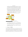
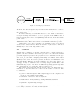
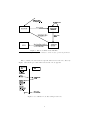
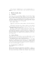
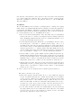
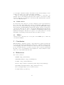
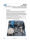
INRIA Rhônes-Alpes Montbonnot
Second Year Internship
from July 13th to August 19th
Internship tutor : Sandrine Avakian, Fabien Jammes
Wireless Sensor Network
Dorian Haglund
<[email protected]>
Montbonnot, August 19, 2011
Contents
1 Context - INRIA
3
2 Internship goals
2.1 Toolchain . . . . . . . . . .
2.2 Sensors Drivers . . . . . . .
2.3 Logging data on a SD card
2.4 Radio device . . . . . . . .
2.5 TDMA . . . . . . . . . . . .
.
.
.
.
.
.
.
.
.
.
.
.
.
.
.
.
.
.
.
.
.
.
.
.
.
.
.
.
.
.
.
.
.
.
.
.
.
.
.
.
.
.
.
.
.
.
.
.
.
.
.
.
.
.
.
.
.
.
.
.
.
.
.
.
.
.
.
.
.
.
.
.
.
.
.
.
.
.
.
.
.
.
.
.
.
.
.
.
.
.
.
.
.
.
.
.
.
.
.
.
.
.
.
.
.
4
5
5
6
6
6
3 Work actually done
3.1 Toolchain . . . . . . . . . .
3.2 Sensors Drivers . . . . . . .
3.3 Logging data on a SD card
3.4 Radio device . . . . . . . .
3.5 TDMA . . . . . . . . . . . .
.
.
.
.
.
.
.
.
.
.
.
.
.
.
.
.
.
.
.
.
.
.
.
.
.
.
.
.
.
.
.
.
.
.
.
.
.
.
.
.
.
.
.
.
.
.
.
.
.
.
.
.
.
.
.
.
.
.
.
.
.
.
.
.
.
.
.
.
.
.
.
.
.
.
.
.
.
.
.
.
.
.
.
.
.
.
.
.
.
.
.
.
.
.
.
.
.
.
.
.
.
.
.
.
.
7
7
8
8
10
10
4 Results
4.1 Sensors drivers . . .
4.2 File System Drivers .
4.3 Running FreeRTOS .
4.4 Radio device . . . .
4.5 TDMA . . . . . . . .
.
.
.
.
.
.
.
.
.
.
.
.
.
.
.
.
.
.
.
.
.
.
.
.
.
.
.
.
.
.
.
.
.
.
.
.
.
.
.
.
.
.
.
.
.
.
.
.
.
.
.
.
.
.
.
.
.
.
.
.
.
.
.
.
.
.
.
.
.
.
.
.
.
.
.
.
.
.
.
.
.
.
.
.
.
.
.
.
.
.
.
.
.
.
.
.
.
.
.
.
.
.
.
.
.
10
10
11
11
11
12
.
.
.
.
.
.
.
.
.
.
.
.
.
.
.
.
.
.
.
.
5 Conclusion
12
6 References
12
7 Appendix
12
2
Introduction
This report details the internship I made during summer 2011 in INRIA Rhônes-Alpes. During the internship I worked on a sensor network platform which can have various applications in sport, healthcare
or robotic fields. For example, if the sensors measure precisely a skier’s
trajectory, it can be recreated numerically and help the skier to improve
his performance. Another example is, if someone has a non functional leg,
the sensors can measure the movements and the forces impulsed by the
sane leg, and recreate it on the deficient leg to simulate a walk.
This platform is called Senslab. Its purpose is to provide a large scale
open wireless sensor network to researchers to enable them to test their
protocols for such networks. Furthermore, the platform offers a set of
tools to help in the design, development, tuning, and experimentation of
real large-scale sensor network applications.
This network is made up of 1024 nodes distributed over 4 INRIA sites
and remotely programmable for scientific research experimentation.
Figure 1: Senslab Network
a
a http://senslab.inrialpes.fr/wp-content/uploads/2010/07/carte.png
So far SWN430 board were used, but to overcome limitations due to
hardware capacities, the INRIA decided to use a more powerful board
based on the STM32 micro-controller. To use this board in the network
the software must be adapted for the new device. This is the part I worked
on.
We will first present the institute, then we will explain my goals. We
will explain the work actually done afterward. Finally, we will discuss the
results obtained and conclude.
1
Context - INRIA
I did my internship at INRIA Rhône-Alpes, located in Montbonnot, Isere France.
It is a state institute of research in computer science and automatic. It’s composed of various research teams and, among other services, a software development support service where I worked named SED. Its purpose is to support
the other teams by providing help for development tools, to create experimental
platforms and to participate in the research teams’ software development. My
supervisors was Sandrine Avakian, who is a generalist engineer in electronic,
3
telecommunication and computer science and Fabien Jammes who is also a generalist engineer specialized in image synthesis. Some of the SED’s members who
had worked on the Senslab project left the INRIA to create their own company
named HiKoB but continued the work they previously did in SED. They wrote
most of the drivers I worked on.
2
Internship goals
My main goal was to implement the same features as the WSN430 on the new
board. Given that their hardware specifications were different, I had to understand hardware behavior and then upgrade the C software efficiently. Figure 2
is a picture of the new card.
Figure 2: La carte STEVAL-MKI062V2
a
a http://www.st.com/internet/evalboard/product/250367.jsp
As you can see in this capture, the board has several devices such as :
• a pression sensor (LPS001DL)
• a temperature sensor (STML75DS2F)
• an accelerometer and a magnetometer (LSM303DLH)
• a gyroscope (LY330ALH)
• a SD slot
From capturing the data with different, to configure and use the operating
system on this micro-controller, a whole set of different features had to be
implemented. So the users could use this more effecient board for their projects.
An example of a project which could use the sensor network is represented in
Figure 3
4
Figure 3: Overall project structure
As shown, the data are captured by the sensors then transformed to be able to
reconstitute the trajectory. My work was focus on the left part of the scheme,
the capture part.
To achieve this target, several things had to be done. First of all, I had so
set up my working environment to be able to program on the STM32 board. I
helped replacing the former board (WSN430) with the new, from the software
point of view.
The embedded processor is a STM32 of the Cortex-M3 family using the
ARM architecture. This board is in fact a benchmark for this new processor.
I firstly had to set up the toolchains to programming on the board, then I
worked on two sensors drivers. After this I tried to log the data to a SD card.
Finally I try to use a radio chip with the card.
2.1
Toolchain
Firstly I had to install the tools that would allow me to compile and run programs on the new card. Since the sensors’ processor are not the same as usual
personal computers processors, the program need to be translated for the specific board. So the whole compilation chain must be redefined, this is called
“cross compilation”. Once the program is compiled, it needs to be written
(flashed) on the card. The service provided an interface for flashing the card
through a JLink. When the program is running on the new card, it has to be
debugged. A way to do this is to use an on-chip debugger, which allow to run
instructions step by step. I worked on a different Operating System (OS) than
the other members of the team who worked on this project.
The software was already known, but I had to figure out which version to
install, how to use them and how to make it work together on a Fedora. The
toolchain was :
• gcc-4.4.4 : Gnu C Compiler. This compiler support cross compilation for
various processor family such as ARM.
• newlib-0.19 : libraries for embedded system.
• binutils-2.20.1 : Binary utilities providing linker and assembler.
• OpenOCD : Open On Chip Debugger.
These programs were already installed and tested on other machines, so I had
to see if they could work on a Fedora Linux system.
5
2.2
Sensors Drivers
At first, I had to test and debug the drivers created for the new card. Functional
drivers implemented by ST Microelectronics for the card already existed, but the
code that we had was not clear enough and and not easy to maintain, plus the
drivers were not efficient enough to match the various applications requirements.
This is why the development team decided to write new ones which were smaller
in term of code size which reduced the memory used.
To communicate with its surrounding peripherals such as the sensors or the
micro-SD slot, the card’s processor needed drivers which could run the various
communication protocols. The various components of the card are not connected
all through the same buses so there are a driver for each bus.
The pressure sensor and accelerometer I worked on used the I 2 C bus. I 2 C
for Inter Integrated Circuit, is a bus to connect the sensor to the processor.
I had to check the communication process between the core and the sensors
through this bus.
The protocol contains many synchronization phases, which were implemented
by busy-waiting algorithms. Another way to solve this issue would be to wake
up the process on an interruption because the I 2 C bus is rather slow and busywaiting is a waste of processor resources. But the team was not experimented
with this I 2 C bus so we decided to take a simple approach first.
2.3
Logging data on a SD card
Once the drivers for the magnetometer and the pressure sensor were completed,
I had to log the data on a micro-SD card. To do so, I debugged and tested the
file system (FAT32) drivers and the file system interface. A file system is a way
to organize data on hard drives like SD cards or hard disk drive. The interface
is used to make the file system transparent to users. This is useful because when
the file system change, most of the programs can remain the same.
Then a real time operating system (FreeRTOS) needed to be installed on
the new card, which would manage the tasks that capture the data and transfer
them either to a SD card or, later, to other boards. Another approach is to
run the tasks alone on the card (without any OS) independently using timer
synchronization. But for only two tasks, this solution complexity is very high.
Indeed, assuming that the timers are correctly synchronized, there is no way to
predict the ISR (Interrupt Service Routine, launched by the timer) duration. If
a timer finishes before the previous ISR ends, that would imply data loss. Not
to mention that if more task end up be added, the problem would become even
more complex.
That is why the service decided to use an OS, which imply more memory
usage, but improve the code clarity and the stability of the running program.
FreeRTOS was chosen as embedded real time OS because it is a very light and
free OS for embedded system and real-time oriented. Moreover it was previously
used by other employees, which means that the code review would be much
easier. Other systems were tested such as Contiki and TinyOS, but for this
application FreeRTOS was better. As a matter of fact, TinyOS is written in
NesC (Network Embedded System C) and is not made for real-time applications
and Contiky has a too heavy kernel because of his various functionality.
6
Figure 4: TDMA divide each frequency channel into multiple time slots
a http://people.seas.harvard.edu/˜jones/cscie129/nu
2.4
a
lectures/lecture3%20/TDMA01.html
Radio device
The card I worked on doesn’t have an integrated radio device. Since the goal is
to set up a wireless sensor network, an external radio module was plugged on
the board.
Once again drivers were needed in order to communicate with the radio.
Drivers were already written for an other board than the STEVAL-MKI062V2,
so I could follow the example of this code and adapt it.
The first step was to make the micro-controller communicate with the radio
module. Then I had to make basic transmission and reception work, to see if
the radio could send data over the network. To test the reception, I was given
an antenna that emitted packed on the required frequency.
2.5
TDMA
TDMA (Time Division Multiple Access) was chosen as the communication protocol at the mac layer. It is a simple protocol based upon time slots allocation
to the network nodes. TDMA was chosen over CSMA because its timings are
more accurate, there is less data loss and is lighter on the battery state (nothing
to do between two time slots).
In this architecture there are two types of nodes, the sensor nodes which use
the sensors to record data and send it to the coordinator node which discover
the new capturing nodes, attribute the time slots and fetch the data. Figure 5
shows the machine state of a sensor node.
7
Figure 5: The node Finite State Machine
aA
a
beacon is message sent by the coordinator to all the nodes to provide its parameters
The coordinator nodes reserved a specific time slot for new node discovery.
Figure 6 shows the procedure when a new sensor node appears.
Figure 6: Coordinator node discovering a new node
8
I had to write the communication protocol for the capturing and the coordinator. Once again, code was provided for other boards, and so was the state
machine.
3
Work actually done
3.1
Toolchain
Since I had to work on a board using an ARM processor and with no display
screen, I started by installing the right compiler in order to be able to flash
the board. Then I had to set up a proxy between the card and my personal
computer in order to use debug utilities such as gdb and display execution traces.
A real time operating system was also needed to run the programs. Since the
development chain had never been installed on a Fedora system, I wrote a quick
tutorial so the team will be able to set it up quickly.
The toolchains contains :
• GCC is the compiler itself, it calls the binutils tools and the newlib library.
It
I learned that on embedded device, you have to map the code, the data, the
ram to specific part of the micro-controller device memory. And so how to write
a linking script which tells gcc how to do so.
FreeRTOS is embedded Operating System, which will be described below.
The various compilation-related software described above and the rather
complex installation procedures to set them up helped me to know the compilation chain better. Furthermore, it get me to know project compilation tools
such as cmake which can generate makefiles (files containing the compilation parameters) from simple text configuration files, and manage new project source
file in a simple way.
3.2
Sensors Drivers
On the first weeks, I worked mostly on I 2 C bus. Firstly I had to become
familiar with the embedded technologies, which I had never studied before. I
had to understand the the code given, and check every step.
The main part of the work was to check if registers were set to correct values
and if the bus commands were sent in the right order. To do this I used GDB
which allow to print the value stored at a given address - to examine registers
- and see where are the infinite waiting loop. Such loops appear if the protocol
is not respected. The protocols were documented in reference documentation of
the board, provided by ST Microelectronics.
3.3
Logging data on a SD card
SD Drivers
When the sensors drivers were functional, the team wanted to be able to to
write the data on a SD card. Drivers for the sd card and for the FAT32 file
system were already written by HiKoB, but not fully tested yet. I had to test
and debug the drivers using a benchmark. The benchmark consisted in writing
9
raw data into various hard-coded locations on the card, and read it afterward
to see if the result was consistent. As a consequence, I had to learn about the
Fat32 file organization, in sectors and clusters, and how to edit he FAT (File
Allocation Table).
FreeRTOS
We used FreeRTOS as the real time operating system to manage the logging
tasks. I had to get familiar with this OS and configure it to match the application
requirements. FreeRTOS configuration consists in editing one file which set the
OS main behaviors such as memory management, size of allocated memory,
process and threads policy, etc. FreeRTOS allowed us to :
• Choose the memory management. Since the tasks don’t need dynamical
memory allocation or deletion, the simplest memory manager (and less
ram-consuming) available was the best choice. In this system all the object
are allocated statically and never freed.
• Set the right stack/heap size. When my code was finished, I had to reduce
the stack given to each task, to optimize memory usage. To do so, I
gradually reduced the allocated memory until the program crash and the
moved back to last good value with a 10% margin for obvious safety reason.
Another approach is to to examine stacks’ task using GDB and see the
deepest address used in the stack. But this approach was complicated and
the code was likely to change, so a too precise analysis was pointless.
• Get the tasks to work together. Tasks can run at different priorities, assuming that the highest priority task preempt on (take the processor from)
the lower priority tasks, I had to deal with starving issue. The tasks run
simultaneously, so I had to deal with all the usual concurrency programming issues, such as race condition, resource starvation, deadlocks, etc
• Test the whole program. Since the several components were already tested
individually, I let the operating system run for hours (a night and half a
day) in order to see if any race condition, stack overflow, or other run-time
related errors occurred.
To write on the sd card, a classis producer-consumer pattern was used :
The data log is made of two steps :
• First, write captured data in a buffer. To do so, a free buffer (not dirty) is
needed. A buffer is dirty when it contains data and has not been written
on the card yet. When a free buffer is chosen, we must access it with
the guarantee that no other tasks are using it. That is why we need a
mutex for this buffer. A mutex is a structure that guarantee the access to
a resource by a only one process at a a time. Once the data are stored on
the hard drive, the buffer is usable and can be chosen by the sensors.
• Second, write a buffer to the SD card. A buffer must be chosen, but among
the dirty buffers some are more filled than others. The more used buffer
is chosen, and once the access is granted by a mutex, access to the buffer
(and lock it), and write it down on the card.
10
Figure 7: Buffers were accessed by two process in a concurrent manner
Actually, the algorithm is more complicated. In fact, there are two mutexes
for each buffer. One to access the buffer header, which describes the buffer’s
state, and one to access to the data itself. This permits to check the buffer
state when the data is locked. This allow to speed up the choosing function,
but increase the complexity.
Once again, the tasks were already written by the SED team but not functional. That is why I needed to first understand the concurrent access to buffers,
and then correct it. This was the more complicated but the more interesting
part of my internship. The SD standards don’t guarantee a stable response time
when writing to the sd, but they do guarantee a maximal response time. This
maximal response time is far too big for the log task to fit in between two captures. To overcome this issue of irregular writing time, it has been decided to
use 15 buffers to prevent data loss. 15 buffers was the best compromise between
memory allocation, and safe writing. If more buffer are used, every task’s stack
must be increased, and with less buffer, the data loss risk is too high.
3.4
Radio device
The first step was to make the micro-controller communicate with the radio
module. To do so, I configured the micro-controller and tried to read registers
into the device, which had predefined values.
The radio device was connected to the board via an SPI bus. A Serial
Peripheral Bus is used to connect a slave (in our case, the radio) to a master
module (the micro-controller). It had to configure ten lines. Using the board
data sheet I had to map the correct line to the micro-controller such as MISO
(Master Input Slave Output), MOSI and the interrupt and timer. I also had
to set the clock for the device. On the board, the main clock goes by various
electronic circuit which slow down the clock such as prescaler – which purpose
is to divide the clock to simulate a lower frequency – or speed it up (like the
Phase locked loop). I retraced all the way the clock went by to finally set the
device clock accordingly.
While setting up the ISR (Interrupt Service Routine). I discovered something
wrong in the linkage script. This script is in charge, among other thing, of setting
the memory outline, and it did not map the NVIC (Nested Vector Interrupt
Controller : which contained the adress of the ISRs) well. I hence learned the
11
script syntax and was able to understand the sections repartition according to
the option given to gcc such as -ffunction-sections or -fdata-sections. These
options allowed to improve the performance of the linkage, but were finally
removed because they caused problems in debug phase.
3.5
TDMA
I did not have enough time to port the TDMA protocols entirely on the new
card. But I wrote the sensor node part, without being able to test it correctly
because the coordinator part was not written and I had only one card. But
I could deduce, from the other card drivers – which were written under more
hardware constraints – the finite states machine.
4
4.1
Results
Sensors drivers
Thanks to the uart bus plugged in my machine’s usb port, I was able to print
the value captured by the sensors live. This can be done by connecting a terminal to the USB port such as minicom or gtkterm. So I was able to see if
the numbers were varying accordingly to what was expected. For example, as I
was rotating the board in order to put an axis toward the ground, I could see
the acceleration (provided by gravity) jump from one axis to the other. I could
test the magnetometer by pulling up electronic device such as mobile phone. In
a similar way, as the temperature sensor is very precise, I could see the values
going up or down as the room was cooling down or warming up. Once the transformation part of the project is done, we will be able to reproduce the board’s
movement because there will be full inertial module running (accelerometer and
gyroscope) and represent the temperature variations.
4.2
File System Drivers
In order to check the drivers for the FAT32 file system, there was two things to
look at. First : if given a certain address on the hard drive we could effectively
write on it. To do so, we first launched the program, and then plugged the card
into a standard computer and ran the Linux dd program which can dump what
it read on a device. By piping the output of dd to an hexadecimal interpreter (
hexdump), we could see if the data was actually there. After this, I had to test
the file system interface, so I created, filled, and closed a file on a program on the
board. Then I mounted the card on a computer, to see if the file was recognize
by the FAT32 driver of the Linux kernel. Then I unmounted the device, and
dumped it to see if the address in the file allocation table (FAT) matched the
effective data address.
4.3
Running FreeRTOS
To test the tasks running on FreeRTOS, I let the logging program run for a
night and half a day, to see if any deadlocks or starvation, occurred. Then I
checked the data on the sd card to see if they were consistent. Even is this test
does not provide any formal guarantee that all cases were covered, it was judged
12
good enough to valid the software. As a matter of fact, if any formal proof were
possible, it would be very complex and time consuming.
I also set several stack size, and switch the priorities, to check the code
stability. As it is, the tasks priorities favors the capture to the data recording.
I tried to make my code stable the other way around, which means to pay the
cost of an additional mutex.
4.4
Radio device
To check if the radio pins were correctly configured, I read some internal register of the radio chip which value were set by hardware. This allow me to
check, in one test, that the VCC (power supply bus), the MISO (Master Input
Slave Output), the MOSI (Master Output Slave Input), and the clock pin were
correctly set. The next two pins to test was the IRQ (interrupt pin) and the
timer pin was correctly set. To do so I simulated a transmission, which would
launch an interruption, and then a reception to see if the packet are correctly
timestamped, and thus proving that the timer is working correctly.
4.5
TDMA
I was not able to run any test on node part of the TDMA protocol since my
code was not finished.
5
Conclusion
This internship contributed greatly to my formation by giving me knowledge
about embedded system and hardware architecture, compilation chain and various debugging tools. He also allowed me to discover how to work on large scale
project, knowing that my code will be reviewed, and so made me understand
the value of a good documentation. He reassured me on my formation because
I met a lot of problems studied in class.
6
References
Site of the tools used :
• INRIA : http://www.inria.fr/
• SED Rhônes-Alpes : http://sed.inrialpes.fr/
• Senslab : http://www.senslab.info/
• Board : http://www.st.com/internet/evalboard/product/250367.jsp
• Real Time Operating System : http://www.freertos.org/
• Proxy debugger http://openocd.berlios.de/web/
• Compiler http://gcc.gnu.org/
13
7
Appendix
STEVAL-MKI062V2 data sheet :
5
4
3.3V Power Management
Vin
R70
Vin
3
2
2
RS (533-1804)
AVX (TAJR225K006RNJ)
Dimension2012-12 metric equal to 0805
Grd 3.3V
D2
D3
+3V3
+3V3
4DM
R25
R26
4.7k
4.7k
USBUF02W6
100 R29
I2C1_SCL
I2C1_SDA
C21
4.7nF
GPIO2_PB0 26
ST_LPR
27
Gyro_PR_RST 57
58
100 R30
+3V3
R72 56R
D4
36 PD/Sleep_LYaw
35 ST_LYaw
34 INT2_ACC
33 INT1_ACC
R31 100
30
29
R32 100
R27
R28
4.7k
4.7k
I2C2_SDA
I2C2_SCL
TP
LY330ALH
DAT2_Ex
DAT3_In
DAT3_Ex
CMD_In
CMD_Ex
CLK_In
CLK_Ex
DAT0_In
DAT1_In
Micro QFN
DAT0_Ex
DAT1_Ex
5
23
7
22
6
17
21
RES
RES
RES
VDD
VDD_DIG_M
27 INT2_ACC
RES
RES
28
3
RES
GND
RES
26 INT1_ACC
Y1
T2
R74 10K
32.768 kHz
4
3
1
2
OSC32_OUT
OSC32_IN
LYaw_Vref
NC
NC
NC
NC
NC
Y
4xOUTY
NC
13
NC
12
R88
Mount 0R LGA 28L
4xINY
NC
NC
GND
4xINX
NC
21
10
11
16
R87
15
0R
R89
0R Not Mount
LPR_Vref
3
9
VDD
ST_LYaw
VREF
OSCIN
R76
Not Mount 1M
LYaw_Vref
JTAG/SWD
10nF
R33
10k
8MHz
11 SDCard_CLK
232
UART2_RX 1
UART2_RTS 3
5
2
4
6
EMIF06-MSD02N16
RS232
UART2_TX
UART2_CTS
+3V3
Male Connector 2x3
Pitch 2.54 mm
2
1
J1
Digikey (WM18900-ND)
Molex 22-05-7025
S4
2
1
3
SWITCH 1X2
D2
EAO 09.03201.02
RS: 115-6283
SMTY5.0A
Farnell: 1608080
Distrelec: 210007
Temperature Sensor
For further details
please refer to datasheet
+3V3
USB_5V
VCC_EXT
J4
10 SDCard_D0
SDCard_D1
Vin
VCC_EXT
R6
10k
R35
10k
Male Connector 2x5
Pitch 1.27 mm
SAMTEC FTSH-105-01-F-D-K
R36
10k
JNTRST
JTMS
JTCK
JTDO
JTDI
RESET#
2
JP1 JUMPER
1
R44
10k
I2C2_SCL 2
nOS/INT
3
4
SDA
VDD
SCL
A0
nOS/INT A1
GND
A2
8
7
A0
6
A1
5
A2
C1
100nF
C40
1
3
5
7
9
10uF 6.3V
C41
100nF
U9
SWD/JTAG
GND
+3V3
J8
+3V3
1
I2C2_SCL 2
I2C2_SDA 4
5
GPIO2_PB0
SPI1_SCK
SPI1_MISO
GPIO1_PA8_MCO
1
3
5
7
9
+3V3
CS
SCL
SDA/MOSI
SA0/MISO
2
4
6
8
10
LPS001DL
I2C Address:
Read: 0xBB
Write: 0xBA
SPI1_CS
SPI1_MOSI
GPIO4_PC7
GPIO3_PC3
INT1
INT2
RES
GND
6INT1_PS
7
8
9
LGA 16
A
COMM. 2x5
Female Connector 2x5
Pitch 2.54 mm
Title
I2C Address:
Read: 0x91
Write: 0x90
+3V3
RS (405-9517)
AVX (TAJR106K006R)
+3V3
J7
2
4
6
8
10
Extended Connector
+3V3
U2
I2C2_SDA 1
B
Pressure Sensor LPS001DL
For further details please
refer to datasheet
GND
Power Selector
GND
Murata (CSTCE8M00G55-R0)
DigiKey (490-1195-1-ND)
RS: 283-961
Farnell: 1615352
HP Filter Disabled:
Assembly R/C3 --> R 0 Ohm
Not Assembly R76 1M Ohm
+3V3
R34
10k
+3V3
12 SDCard_CMD
OSCOUT
10nF
HP Filter Enabled:
Assembly R/C3 --> C 4.7 uF
Assembly R76 1M Ohm
15
13 SDCard_D3
Y3
LYaw_Vref
LPR_Vref
HP Filter Enabled:
Assembly R/C2 --> C 4.7 uF
Assembly R85 1M Ohm
HP Filter Disabled:
Assembly R/C2 --> R 0 Ohm
Not Assembly R85 1M Ohm
14 SDCard_D2
Yaw_OUT
C55
7
LGA 10
12 pF
DigiKey (300-8633-1-ND)
Farnell: 1457098
Citizen (CM130-32.768KDZF-UT)
R75
27k
PR_Y_1xOUT
C63
R85
Not Mount
1M
C17
12 pF
LP Filter
(Reccomended)
6
LP Filter
(Reccomended)
R83 27k
Not Mount
R84 0R
18
22 LPR_Vref
24 Gyro_PR_RST
9
19
27 ST_LPR
28 PD/Sleep_LPR
17
VCONT
FILTVDD
VREF
ST
HP
VDD
VDD
PD/Sleep
NC
RES
6
Default 1
0R
HP Filter
(Optional)
Default: R --> O Ohm
R/C2
R 0 / C 4.7uF
20
PR_Y_4xOUT 14
16
9
C
OSCILLATORS
TY
Test Point:
Vero technologies: 20-2137 Yaw_OUT
RS:101-2391
C50 10nF
TP Yaw_OUT
GND
RES
RES
GND
8
5
2
3PR_Y_1xOUT
LPR430AL
OUTY
2
7
SDCard_D1_PC9
VCC
DAT2_In
1
PR_Y_OUT
R78
PR_Y_OUT
R79
10K
1
6
SDCard_D0_PC8
RDATA_VCC
RDAT3_GND
GND
SDCard_CLK_PC12
WP/CD
17
4
5
4
HP Filter Disabled:
LPR_Vref
Assembly R/C1 --> R 0 Ohm
Not Assembly R81 1M Ohm
U14
SDCard_CMD_PD2
2
3
R86
0R
HP Filter Enabled:
Assembly R/C1 --> C 4.7 uF
Not
Assembly R81 1M Ohm
NC
LPR_Vref
+3V3
PR_X_4xOUT
8SDCard_D1
7SDCard_D0
6
5SDCard_CLK
4
3SDCard_CMD
2SDCard_D3
1SDCard_D2
4xOUTX
10nF
DAT1
DAT0
VSS
CLK
VDD
CMD
CD/DAT3
DAT2
8
R81
1M
Not Mount
microSD
Hirose Electric:
DM3AT-SF-PEJ
Digikey:
HR1939CT-ND
U13
OUTX
7
1
27k
23
C62
CN2
HP Filter
(Optional)Default: R --> O Ohm
R/C1
R 0 / C 4.7uF
R80
25
LP Filter
(Reccomended)
PR_X_1xOUT
26
SW2
SW PUSHBUTTON-DPST
RS (505-9186)
C&K (Y78B22110FP)
GND
OUTZ
1PR_Y_4xOUT
R82 0R
Not Mount
RS (505-9186)
C&K (Y78B22110FP) GND
RES
RES
TP PR_Y_OUT
C58 10nF
C59
470nF
X
RST
VDD
10
ST
TP LPR_Vref
DigiKey:
587-1093-1-ND
2
0R
B
SW PUSHBUTTON-DPST
25 I2C1_SDA
LSM303DLH
Default: R --> O Ohm
HP Filter
(Optional)
R/C3
R 0 / C 4.7uF
VCONT
U12
GND
C57
100nF
10uF 6.3V
1PR_X_4xOUT
C25
100nF
24 I2C1_SCL
TP LYaw_Vref
C52
100nF
PD/Sleep
10uF 6.3V
TG
TP Ground
3PR_X_1xOUT
A
C53
470nF
C56
TP PR_X_OUT
R77
3
LGA 28L
DigiKey:
587-1093-1-ND
Test Point:
Vero technologies: 20-2137
RS:101-2391 T4
LPR_Vref
RS (405-9517)
AVCC
AVX (TAJR106K006R)
Default 1
2
INT2
18 Mag_DRDY
C16
PR_X_OUT
1
RES
19 I2C1_SDA
1-AXIS Gyroscope LY330ALH (Yaw)
For further details please refer to datasheet
and User Manual
5
R22
10K
SDCard_D3_PC11
INT1
GND
2-AXIS Gyroscope
LPR430AL (Roll/Pitch)
For further details please refer to datasheet and User Manual
Push_Button
SDCard_D2_PC10
13
SDA_A
RES
RS (405-9517) AVCC
AVX (TAJR106K006R)
PR_X_OUT
R21
10K
microSD
SCL_A
RES
R73 56R
GREEN
Kingbright KP2012MGC
RS: 466-3778
Farnell: 8529906
LED 0805
+3V3
GND
DRDY_M
Y
SA0_A
+3V3
GND
TR
GND
VDD_IO_A
RES
PB15
PB14
PB13
PB12
PB11
PB10
+3V3
SDA_M
C1
C51
GND
+3V3
C24
100nF
SET1
4
11
I2C Address Magnetometer:
Read: 0x3D
Write: 0x3C
User_LED
RED
Kingbright KP2012SURC
RS: 466-3829
Farnell: 8529930
LED 0805
RESET#
15
16
SA0_A
+3V3
2.2uF
I2C Address Accelerometer:
Read: 0x33
Write: 0x32
LED RESET PS BUTTON
D3
RES_CAP
C49
GND
12
18
63
47
31
STM32F103RET7
SDCard_CLK_PC12
SDCard_D3_PC11
SDCard_D2_PC10
SDCard_D1_PC9
SDCard_D0_PC8
GPIO4_PC7
nOS/INT
LYaw_Vref
Yaw_OUT
GPIO3_PC3
LPR_Vref
PR_Y_OUT
PR_X_OUT
NC
13 VDDA
19 VDD_4
64 VDD_3
48 VDD_2
32 VDD_1
1 VBAT
STM32F103RET7
PB0
PB1
PB5
PB6
PB7
PB8
PB9
59
Mag_DRDY 61
User_LED 62
53
52
51
40
39
38
37
25
24
11
10
9
8
20 I2C1_SCL
16
15
14
13
USBDM 3
USB_DISCONNECT
PC12
PC11
PC10
PC9
PC8
PC7
PC6
PC5
PC4
PC3
PC2
PC1
PC0
NC
GND
PA0-WKUP
PA1
PA2
PA3
PA4
PA5
PA6
PA7
PA8
PA9
PA10
PA11
PA12
SCL_M
VDD
VDD
RES
VDD_IO
ID nc
GND
SHELL
SHELL
SHELL
SHELL
5
C48
2.2uF
SET2
3
10
11
12
2
12
10
UART2_CTS 14
UART2_RTS 15
UART2_TX 16
UART2_RX 17
SPI1_CS
20
SPI1_SCK 21
SPI1_MISO 22
SPI1_MOSI 23
GPIO1_PA8_MCO 41
INT1_PS
42
USB_DISCONNECT 43
USBDM
44
USBDP
45
C35
100nF
U5 SOTT323-6L
6DP
D1
D4
USBDP 1
C47
100nF
C46
100nF
2
4
5
6
7
8
9
+3V3
50 JTDI
49 JTCK
46 JTMS
56 JNTRST
55 JTDO
54 SDCard_CMD_PD2
2 Push_Button
2
GND
PA15-JTDI
PA14-JTCK
PA13-JTMS
PB4-JNTRST
PB3-JTDO
PD2
PC13-TAMPER-RTC
VDD_4
C34
100nF
GND
USB_miniB
VBUS
DM
DP
1V8 +3V3
D
LQFP-64
1
GND
PC14-OSC32_IN
PC15-OSC32_OUT
PD0 OSC_IN
PD1 OSC_OUT
NRST
BOOT0
PB2-BOOT1
9
1uF 6.3V
CN1
1
2
3
+3V3
U11
4
USB_5V
U6
OSC32_IN
3
OSC32_OUT 4
OSCIN
5
OSCOUT
6
RESET#
7
BOOT0
60
PD/Sleep_LPR 28
C29
100nF
+3V3
GND
AVCC
C44
100nF
10uF 6.3V
8
C66
10nF
+3V3
VDD_1
C26
100nF
RS (515-1995)
Molex (54819-0572)
R23
1M
RS (405-9517)
AVX (TAJR106K006R)
14
GND
RS (405-7779)
AVX (TACL105M006R)
C27 Dimension 1608-10
metric equal to 0603
2
4
C65
1uF
+3V3
VBAT
5
VOUT
BYPS
VIN
SOT23-5L
1V8
VDDA
Vdd_4
Vdd_3
Vdd_2
Vdd_1
VBAT
INH
LD3985M18R
VSSA
Vss_4
Vss_3
Vss_2
Vss_1
3
GND
Place near MCU
VDD_2
C
C20
1uF 6.3V
C45
1
+3V3
L2 30 Ohm 3A
1
2
Wurth Electronics:
74279206
RS: 358-6765
DM
DP
C19
100nF
GND
AVCC
USB
GND
Vin
U15
C13
10nF
RS (405-7779)
AVX (TACL105M006R)
Dimension 1608-10 metric
equal to 0603
VDDA
RS (405-9517)
AVX (TAJR106K006R)
Dimension2012-12 metric
C23
10uF 6.3V equal to 0805
C22
100nF
PD/Sleep_LYaw 8
3
INH
C43
2.2uF 6.3V
AVCC
+3V3
VDD_3
GND
BYPS
2
4
R69
0R
+3V3
5
SOT23-5L
C64
33nF
D
10K
BOOT0
3
Default 3
LDS3985M33R
VOUT
Z
VIN
X
U10
1
C42
1uF
1
LSM303DLH
6-axis Geomagnetic Module
For further details please refer to datasheet
MCU STM32F103
For further details please refer to datasheet
1V8
1
STLM75DS2F
STEVAL-MKI062V2 STMicroelectronics
Size
Document Number
Custom
Rev
1.0
iNEMO V2
Date:
5
4
3
2
Figure 8: STEVAL-MKI062V2 data sheet
14
Thursday, April 08, 2010
Sheet
1
2
of
2