1
Intel® Xeon® Processor E5-2400 v3
Product Family
Datasheet, Volume One: Electrical
Volume 1 of 2
January 2015
Reference Number:331592-001
You may not use or facilitate the use of this document in connection with any infringement or other legal analysis concerning Intel
products described herein. You agree to grant Intel a non-exclusive, royalty-free license to any patent claim thereafter drafted which
includes subject matter disclosed herein.
All information provided here is subject to change without notice. Contact your Intel representative to obtain the latest Intel product
specifications and roadmaps.
Intel technologies may require enabled hardware, specific software, or services activation. Check with your system manufacturer or
retailer.
No license (express or implied, by estoppel or otherwise) to any intellectual property rights is granted by this document.
The Intel® Xeon® Processor E5-2400 v3 Product Family may contain design defects or errors known as errata which may cause the
product to deviate from published specifications. Current characterized errata are available on request.
Contact your local Intel® sales office or your distributor to obtain the latest specifications and before placing your product order.
Copies of documents which have an order number and are referenced in this document, or other Intel literature, may be obtained by
calling 1-800-548-4725, or go to: http://www.intel.com/#/en_US_01
Hyper-Threading Technology requires a computer system with a processor supporting HT Technology and an HT Technology enabled
chipset, BIOS and operating system. Performance will vary depending on the specific hardware and software you use. For more
information including details on which processors support HT Technology, see
http://www.intel.com/products/ht/hyperthreading_more.htm.
Enabling Execute Disable Bit functionality requires a PC with a processor with Execute Disable Bit capability and a supporting operating
system. Check with your PC manufacturer on whether your system delivers Execute Disable Bit functionality.
Intel® Virtualization Technology requires a computer system with an enabled Intel® processor, BIOS, virtual machine monitor (VMM)
and, for some uses, certain computer system software enabled for it. Functionality, performance or other benefits will vary depending
on hardware and software configurations and may require a BIOS update. Software applications may not be compatible with all
operating systems. Please check with your application vendor.
Intel® Turbo Boost Technology requires a PC with a processor with Intel Turbo Boost Technology capability. Intel Turbo Boost
Technology performance varies depending on hardware, software and overall system configuration. Check with your PC manufacturer
on whether your system delivers Intel Turbo Boost Technology. For more information, see
http://www.intel.com/technology/turboboost.
No computer system can provide absolute security under all conditions. Intel® Trusted Execution Technology (Intel® TXT) requires a
computer with Intel® Virtualization Technology, an Intel TXT-enabled processor, chipset, BIOS, Authenticated Code Modules and an
Intel TXT-compatible measured launched environment (MLE). Intel TXT also requires the system to contain a TPM v1.s. For more
information, visit http://www.intel.com/technology/security
The Processor Spec Finder at http://ark.intel.com or contact your Intel representative for more information.
64-bit computing on Intel architecture requires a computer system with a processor, chipset, BIOS, operating system, device drivers
and applications enabled for Intel® 64 architecture. Performance will vary depending on your hardware and software configurations.
Consult with your system vendor for more information.
Δ Intel processor numbers are not a measure of performance. Processor numbers differentiate features within each processor family,
not across different processor families. See http://www.intel.com/products/processor_number for details.
I2C is a two-wire communications bus/protocol developed by Philips. SMBus is a subset of the I2C bus/protocol and was developed by
Intel. Implementations of the I2C bus/protocol may require licenses from various entities, including Philips Electronics N.V. and North
American Philips Corporation.
Intel, Xeon, Enhanced Intel SpeedStep Technology, Core, and the Intel logo are trademarks of Intel Corporation in the U. S. and other
countries.
*Other names and brands may be claimed as the property of others.
Copyright © 2009-2015, Intel Corporation. All rights reserved.
Intel® Xeon® Processor E5-2400 v3 Product Family
Datasheet Volume One
2
Table of Contents
1
Overview ................................................................................................................... 7
1.1
Introduction ....................................................................................................... 7
1.3
Terminology ....................................................................................................... 8
1.2
Related Documents ............................................................................................. 8
1.4
Processor Feature Overview................................................................................ 12
1.4.1 Core Feature Overview............................................................................ 12
1.5
Interface Feature Overview................................................................................. 12
1.5.1 System Memory ..................................................................................... 12
1.5.2 PCI Express* ......................................................................................... 13
1.5.3 Direct Media Interface Gen 2 (DMI2)......................................................... 13
1.5.4 Intel® QuickPath Interconnect (Intel® QPI) .............................................. 13
1.5.5 Platform Environment Control Interface (PECI) ........................................... 13
1.6
Package Summary............................................................................................. 13
1.7
Statement of Volatility (SOV) .............................................................................. 14
1.8
State of Data .................................................................................................... 14
2
Electrical Specifications ........................................................................................... 15
2.1
Integrated Voltage Regulators............................................................................. 15
2.2
Processor Signaling ........................................................................................... 15
2.2.1 System Memory Interface Signals............................................................. 15
2.2.2 PCI Express* Signals .............................................................................. 15
2.2.3 DMI2/PCI Express* Signals...................................................................... 15
2.2.4 Intel® QuickPath Interconnect (Intel® QPI) ............................................... 15
2.2.5 Platform Environmental Control Interface (PECI) ........................................ 16
2.2.5.1 Input Device Hysteresis ............................................................. 16
2.2.6 System Reference Clocks (BCLK{0/1}_DP, BCLK{0/1}_DN)......................... 16
2.2.7 JTAG and Test Access Port (TAP) Signals ................................................... 17
2.2.8 Processor Sideband Signals ..................................................................... 17
2.2.9 Power, Ground and Sense Signals............................................................. 17
2.2.9.1 Power and Ground Lands ........................................................... 17
2.2.9.2 Decoupling Guidelines ............................................................... 17
2.2.9.3 Voltage Identification (VID)........................................................ 18
2.2.10 Reserved or Unused Signals..................................................................... 18
2.3
Signal Group Summary ...................................................................................... 19
2.4
Power-On Configuration (POC) Options................................................................. 22
2.5
Fault Resilient Booting (FRB)............................................................................... 23
2.6
Mixing Processors.............................................................................................. 24
2.7
Flexible Motherboard Guidelines (FMB) ................................................................. 24
2.8
Absolute Maximum and Minimum Ratings ............................................................. 25
2.8.1 Storage Condition Specifications............................................................... 25
2.9
DC Specifications .............................................................................................. 26
2.9.1 Voltage and Current Specifications............................................................ 26
2.9.2 VCCIN Power Delivery for Integrated Voltage Regulators ............................. 27
2.9.3 Die Voltage Validation ............................................................................. 29
2.9.3.1 VCCIN Overshoot Specifications .................................................. 29
2.9.4 Signal DC Specifications .......................................................................... 30
2.9.4.1 PCI Express* DC Specifications ................................................... 34
2.9.4.2 DMI2/PCI Express* DC Specifications .......................................... 35
2.9.4.3 Intel® QuickPath Interconnect DC Specifications........................... 35
2.9.4.4 Reset and Miscellaneous Signal DC Specifications .......................... 35
2.10 System Reference Clock (BCLK{0/1}) Waveforms ................................................. 35
2.11 Signal Quality ................................................................................................... 37
2.11.1 DDR3 Signal Quality Specifications ........................................................... 38
Intel® Xeon® Processor E5-2400 v3 Product Family
Datasheet Volume One
3
2.11.2
2.11.3
2.11.4
2.11.5
2.12
I/O Signal Quality Specifications............................................................... 38
Intel® QuickPath Interconnect Signal Quality Specifications ......................... 38
Input Reference Clock Signal Quality Specifications..................................... 38
Overshoot/Undershoot Tolerance.............................................................. 38
2.11.5.1 Overshoot/Undershoot Magnitude ............................................... 39
2.11.5.2 Overshoot/Undershoot Pulse Duration ......................................... 39
2.11.5.3 Activity Factor .......................................................................... 39
2.11.5.4 Reading Overshoot/Undershoot Specification Tables ...................... 40
2.11.5.5 Compliance to Overshoot/Undershoot Specifications ...................... 40
C-State Power .................................................................................................. 42
3
Signal Descriptions .................................................................................................. 43
3.1
System Memory Interface Signals........................................................................ 43
3.2
PCI Express* Based Interface Signals................................................................... 44
3.3
DMI2/PCI Express* Port 0 Signals ....................................................................... 45
3.4
Intel® QuickPath Interconnect Signals ................................................................. 45
3.5
PECI Signal ...................................................................................................... 46
3.6
System Reference Clock Signals .......................................................................... 46
3.7
JTAG and TAP Signals ........................................................................................ 46
3.8
Serial VID Interface (SVID) Signals...................................................................... 46
3.9
Processor Asynchronous Sideband and Miscellaneous Signals .................................. 47
3.10 Processor Power and Ground Supplies .................................................................. 49
4
Processor Land Listing............................................................................................. 51
4.1
Land Listing by Name ........................................................................................ 51
Figures
1-1
2-1
2-2
2-3
2-4
2-5
2-6
2-7
2-8
Two-Socket Processor Platform ........................................................................... 12
Input Device Hysteresis ..................................................................................... 16
VCCIN Static and Transient Tolerance Loadlines .................................................... 29
VCCIN Overshoot Example Waveform .................................................................. 30
BCLK{0/1} Differential Clock Crosspoint Specification ............................................ 35
BCLK{0/1} Differential Clock Measurement Points for Duty Cycle and Period ............. 36
BCLK{0/1} Differential Clock Measurement Points for Edge Rate.............................. 36
BCLK{0/1} Differential Clock Measurement Point for Ringback ................................ 36
BCLK{0/1} Single Ended Clock Measurement Points for Absolute Cross Point
and Swing ........................................................................................................ 37
2-9
BCLK{0/1} Single Ended Clock Measurement Points for Delta Cross Point ................. 37
2-10 Maximum Acceptable Overshoot/Undershoot Waveform.......................................... 41
Tables
1-1
1-3
1-2
2-1
2-2
2-3
2-4
2-5
2-6
2-7
2-8
2-9
2-10
2-11
Processor Datasheet Volume Structure .................................................................. 7
Related Documents and Specifications.................................................................... 8
Processor Documents........................................................................................... 8
Power and Ground Lands.................................................................................... 17
SVID Address Usage .......................................................................................... 18
Signal Description Buffer Types ........................................................................... 19
Signal Groups ................................................................................................... 19
Signals with On-Die Termination ......................................................................... 22
Power-On Configuration Option Lands .................................................................. 22
Fault Resilient Booting (Output Tri-State) Signals .................................................. 23
Processor Absolute Minimum and Maximum Ratings ............................................... 25
Storage Condition Ratings .................................................................................. 25
Voltage Specification.......................................................................................... 26
Processor Power Supply Current Specifications ...................................................... 27
Intel® Xeon® Processor E5-2400 v3 Product Family
Datasheet Volume One
4
2-12
2-13
2-14
2-15
2-16
2-17
2-18
2-19
2-20
2-21
2-22
2-23
2-24
3-1
3-2
3-3
3-4
3-5
3-6
3-7
3-8
3-9
3-10
3-11
3-12
3-13
3-14
4-1
Processor VCCIN Static and Transient Tolerance .................................................... 28
VCCIN Overshoot Specifications .......................................................................... 29
DDR3 and DDR3L Signal DC Specifications............................................................ 30
PECI DC Specifications ....................................................................................... 31
System Reference Clock (BCLK{0/1}) DC Specifications ......................................... 32
SMBus DC Specifications .................................................................................... 32
JTAG and TAP Signals DC Specifications ............................................................... 33
Serial VID Interface (SVID) DC Specifications........................................................ 33
Processor Asynchronous Sideband DC Specifications .............................................. 34
Miscellaneous Signals DC Specifications................................................................ 34
Processor I/O Overshoot/Undershoot Specifications ............................................... 38
Processor Sideband Signal Group Overshoot/Undershoot Tolerance .......................... 40
Processor Package C-State Power Specifications .................................................... 42
Memory Channel DDR1, DDR2, DDR3................................................................... 43
Memory Channel Miscellaneous ........................................................................... 44
PCI Express* Port 1 Signals ................................................................................ 44
PCI Express* Port 3 Signals ................................................................................ 44
PCI Express* Miscellaneous Signals ..................................................................... 45
DMI2 and PCI Express Port 0 Signals ................................................................... 45
Intel® QPI Port Signals ...................................................................................... 45
PECI Signal ...................................................................................................... 46
System Reference Clock (BCLK) Signals ............................................................... 46
JTAG and TAP Signals ........................................................................................ 46
SVID Signals .................................................................................................... 46
Processor Asynchronous Sideband Signals ............................................................ 47
Miscellaneous Signals ........................................................................................ 49
Power and Ground Signals .................................................................................. 49
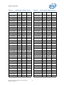
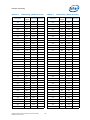
Land Listing...................................................................................................... 51
Intel® Xeon® Processor E5-2400 v3 Product Family
Datasheet Volume One
5
Revision History
Revision
Number
001
Description
Initial Release
Intel® Xeon® Processor E5-2400 v3 Product Family
Datasheet Volume One
Revision Date
January 2015
6
Overview
1
Overview
1.1
Introduction
Intel® Xeon® Processor E5-2400 v3 Product Family Datasheet - Volume One provides
DC electrical specifications, signal definitions and an overview of processor interfaces.
This document is intended to be distributed as a part of a two volume set. The structure
and scope of the volumes is provided in Table 1-1.
The Intel® Xeon® Processor E5-2400 v3 Product Family is the next generation of
64-bit, multi-core server-class processors built on 22-nanometer process technology.
Throughout this document, the Intel® Xeon® Processor E5-2400 v3 Product Family
may be referred to as simply the processor. This processor family is based on the lowpower, high performance Haswell processor microarchitecture to be paired with a
Platform Controller Hub (PCH). The Intel® Xeon® Processor E5-2400 v3 Product
Family is targeted for embedded server, communications and storage applications.
This processor features one Intel® QuickPath Interconnect point-to-point link capable
of up to 8.0 GT/s, 24 lanes of PCI Express* 3.0 capable of 8.0 GT/s, and 4 lanes of
DMI2/PCI Express* 2.0 interface with a peak transfer rate of 5.0 GT/s. The processor
supports up to 46 bits of physical address space and 48-bit of virtual address space.
This processor family incorporates an integrated memory controller (IMC) and
integrated I/O (IIO) including PCI Express* and DMI2) on a single silicon die.
Table 1-1.
Processor Datasheet Volume Structure
Volume One: Electrical
•
Overview
•
Signal Descriptions
•
Electrical Specifications
•
Processor Land Listing
Volume Two: Registers
•
Configuration Process and Registers Overview
•
Configuration Space Registers
•
Model Specific Registers (MSR)
Intel® Xeon® Processor E5-2400 v3 Product Family
Datasheet Volume One
7
Overview
1.2
Related Documents
The following documents provide additional information related to system design with the Intel®
Xeon® Processor E5-2400 v3 Product Family.
Table 1-2.
Processor Documents
Document
Number/
Location1
Document
Table 1-3.
Intel® Xeon® Processor E5 v3 Product Families Datasheet Volume 2; Registers
intel.com
Intel® Xeon® Processor E5-2400 v3 Product Families Thermal/Mechanical Specification
and Design Guide (TMSDG)
intel.com
Related Documents and Specifications
Document
Document Number/ Location
Advanced Configuration and Power Interface Specification 3.0
http://www.acpi.info
PCI Local Bus Specification 3.0
http://www.pcisig.com/specifications
PCI Express Base Specification - Revision 2.1 and 1.1
PCI Express Base Specification - Revision 3.0
http://www.pcisig.com
System Management Bus (SMBus) Specification
http://smbus.org/
DDR3 SDRAM Specification
http://www.jedec.org
Low (JESD22-A119) and High (JESD-A103) Temperature Storage Life
Specifications
http://www.jedec.org
Intel® 64 and IA-32 Architectures Software Developer's Manuals
• Volume 1: Basic Architecture
• Volume 2A: Instruction Set Reference, A-M
• Volume 2B: Instruction Set Reference, N-Z
• Volume 3A: System Programming Guide
• Volume 3B: System Programming Guide
Intel® 64 and IA-32 Architectures Optimization Reference Manual
1.3
http://www.intel.com/products/proce
ssor/manuals/index.htm
Intel® Virtualization Technology Specification for Directed I/O
Architecture Specification
http://www.intel.com/content/dam/w
ww/public/us/en/documents/productspecifications/vt-directed-io-spec.pdf
Intel® Trusted Execution Technology Software Development Guide
www.intel.com/technology/security
National Institute of Standards and Technology NIST SP800-90
http://csrc.nist.gov/publications/Pubs
SPs.html
Terminology
Term
ASPM
Description
Active State Power Management
BMC
Baseboard Management Controllers
Cbo
Cache and Core Box. It is a term used for internal logic providing ring interface to
LLC and Core.
DDR3
Third generation Double Data Rate SDRAM memory technology that is the
successor to DDR2 SDRAM
DMA
Direct Memory Access
DMI
Direct Media Interface
DMI2
Direct Media Interface Gen 2
Intel® Xeon® Processor E5-2400 v3 Product Family
Datasheet Volume One
8
Overview
Term
DTS
Description
Digital Thermal Sensor
ECC
Error Correction Code
Intel®
®
Enhanced
SpeedStep
Technology
Allows the operating system to reduce power consumption when performance is
not needed.
Execute Disable Bit
The Execute Disable bit allows memory to be marked as executable or nonexecutable, when combined with a supporting operating system. If code
attempts to run in non-executable memory the processor raises an error to the
operating system. This feature can prevent some classes of viruses or worms
that exploit buffer overrun vulnerabilities and can thus help improve the overall
security of the system. See the Intel® 64 and IA-32 Architectures Software
Developer's Manuals for more detailed information.
FIVR
Fully Integrated the Voltage Regulator. Internal DC-to-DC voltage regulators
integrated into processor to provide various voltage levels.
Flit
Flow Control Unit. The Intel® QPI Link layer’s unit of transfer; 1 Flit = 80-bits.
Functional Operation
Refers to the normal operating conditions in which all processor specifications,
including DC, AC, system bus, signal quality, mechanical, and thermal, are
satisfied.
IMC
Integrated Memory Controller. System memory controller that is integrated in
the processor die.
IIO
The Integrated I/O Controller. An I/O controller that is integrated in the
processor die.
Intel® ME
Intel® Management Engine (Intel® ME)
Intel® QuickData
Technology
Intel® QuickData Technology is a platform solution designed to maximize the
throughput of server data traffic across a broader range of configurations and
server environments to achieve faster, scalable, and more reliable I/O.
Intel® QuickPath
Interconnect (Intel® QPI)
A cache-coherent, link-based Interconnect specification for Intel processors,
chipsets, and I/O bridge components.
Intel® 64 Technology
64-bit memory extensions to the IA-32 architecture. Further details on Intel® 64
architecture and programming model can be found at
http://developer.Intel.com/technology/Intel®64
Intel® Turbo Boost
Technology
Intel® Turbo Boost Technology is a way to automatically run the processor core
faster than the marked frequency if the part is operating under power,
temperature, and current specifications limits of the Thermal Design Power
(TDP). This results in increased performance of both single and multi-threaded
applications.
Intel® TXT
Intel® Trusted Execution Technology
®
Intel Virtualization
Technology (Intel® VT)
Processor virtualization which when used in conjunction with Virtual Machine
Monitor software enables multiple, robust independent software environments
inside a single platform.
Intel® VT-d
Intel® Virtualization Technology (Intel® VT) for Directed I/O. Intel® VT-d is a
hardware assist, under system software (Virtual Machine Manager or OS)
control, for enabling I/O device virtualization. Intel® VT-d also brings robust
security by providing protection from errant DMAs by using DMA remapping, a
key feature of Intel® VT-d.
Integrated Heat Spreader
(IHS)
A component of the processor package used to enhance the thermal
performance of the package. Component thermal solutions interface with the
processor at the IHS surface.
Jitter
Any timing variation of a transition edge or edges from the defined Unit Interval
(UI).
IOV
I/O Virtualization
LGA1356 Socket
The 1356-land FCLGA package mates with the system board through this surface
mount, 1356-contact socket.
LLC
Last Level Cache
LRDIMM
Load Reduced Dual In-line Memory Module
NCTF
Non-Critical to Function: NCTF locations are typically redundant ground or noncritical reserved, so the loss of the solder joint continuity at end of life conditions
will not affect the overall product functionality.
Intel® Xeon® Processor E5-2400 v3 Product Family
Datasheet Volume One
9
Overview
Term
Description
NEBS
Network Equipment Building System. NEBS is the most common set of
environmental design guidelines applied to telecommunications equipment in the
United States.
PCH
Platform Controller Hub. The next generation chipset with centralized platform
capabilities including the main I/O interfaces along with display connectivity,
audio features, power management, manageability, security and storage
features.
PCU
Power Control Unit
PCI Express* 3.0
PCI Express* Generation 3.0
The third generation PCI Express* specification that operates at twice the speed
of PCI Express* 2.0 (8 Gb/s). PCI Express* 3.0 is backward compatible with PCI
Express* 1.0 and 2.0.
PCI Express* 2.0
PCI Express* Generation 2.0
PCI Express*
PCI Express* Generation 2.0/3.0
PECI
Platform Environment Control Interface
Phit
Physical Unit. Intel® QPI terminology defining units of transfer at the physical
layer. 1 Phit is equal to 20 bits in ‘full width mode’ and 10 bits in ‘half width
mode’
Processor
The 64-bit, single-core or multi-core component (package)
Core
A functional element of the processor capable of executing instructions. Each
core has an instruction cache, data cache, and 256-KB L2 cache. All execution
cores share the L3 cache.
RDIMM
Registered Dual In-line Module
Rank
A unit of DRAM corresponding four to eight devices in parallel, ignoring ECC.
These devices are usually, but not always, mounted on a single side of a DDR3
DIMM.
SCI
System Control Interrupt. Used in ACPI protocol.
SSE
Intel® Streaming SIMD Extensions (Intel® SSE)
SKU
Stock Keeping Unit (SKU) identifying a particular model having unique attributes.
Electrical, power and thermal specifications for these SKU’s are based on specific
use condition assumptions.
SMBus
System Management Bus. A two-wire interface through which simple system and
power management related devices can communicate with the rest of the
system. It is based on the principals of the operation of the I2C* two-wire serial
bus from Philips Semiconductor.
Storage Conditions
A non-operational state. The processor may be installed in a platform, in a tray,
or loose. Processors may be sealed in packaging or exposed to open air. Under
these conditions, processor land contacts s should not be connected to any
supply voltages, have any I/O buffers biased or receive any clocks. Upon
exposure to “free air” (i.e., unsealed packaging or a device removed from
packaging material) the processor must be handled in accordance with moisture
sensitivity labeling (MSL) as indicated on the packaging material.
TAC
Thermal Averaging Constant
TDP
Thermal Design Power
TSOD
Thermal Sensor on DIMM
UDIMM
Unbuffered Dual In-line Module
Uncore
The portion of the processor comprised of the shared cache, IMC, HA, PCU,
UBox, and Intel® QPI link interface.
Unit Interval
Signaling convention that is binary and unidirectional. In this binary signaling,
one bit is sent for every edge of the forwarded clock, whether it be a rising edge
or a falling edge. If a number of edges are collected at instances t1, t2, tn,...., tk
then the UI at instance “n” is defined as:
UI
n
= t n- t
n
-1
VCCIN
Voltage rail supplies the input source to the integrated voltage regulators.
VSS
Processor ground
Intel® Xeon® Processor E5-2400 v3 Product Family
Datasheet Volume One
10
Overview
Term
Description
VCCD
DDR3 power supply for the processor system memory interface.
x1
Refers to a Link or Port with one Physical Lane
x4
Refers to a Link or Port with four Physical Lanes
x8
Refers to a Link or Port with eight Physical Lanes
x16
Refers to a Link or Port with sixteen Physical Lanes
Intel® Xeon® Processor E5-2400 v3 Product Family
Datasheet Volume One
11
Overview
1.4
Processor Feature Overview
1.4.1
Core Feature Overview
• Up to 10 physical cores
• Each core supports two threads (Intel® Hyper-Threading Technology), up to 20
threads per socket
• 32-KB instruction and 32-KB data first-level cache (L1) for each core
• 256-KB shared instruction/data mid-level (L2) cache for each core
• Up to 25 MB last level cache (LLC): up to 2.5 MB per core instruction/data last level
cache (LLC), shared among all cores
A rudimentary block diagram is illustrated in Figure with two processors
interconnected to a Platform Controller Hub (PCH).
Figure 1-1.
Two-Socket Processor Platform
1.5
Interface Feature Overview
This section presents a limited high-level overview of the physical interfaces of the
Intel® Xeon® Processor E5-2400 v3 Product Family.
1.5.1
System Memory
• Three DDR3 channels
• DDR3 standard I/O Voltage of 1.5 V and DDR3 Low Voltage of 1.35 V
• 64-bit wide data plus 8-bits of ECC support for each channel
• Data transfer rates of 800, 1066, 1333, and 1600 MT/s
• Unbuffered DDR3 and registered DDR3 DIMMs
• 1Gb, 2Gb and 4Gb DDR3 DRAM technologies are supported for these devices:
— UDIMMs x8, x16
— RDIMMs x4, x8
Intel® Xeon® Processor E5-2400 v3 Product Family
Datasheet Volume One
12
Overview
— Up to 8 ranks supported per memory channel, 1, 2 or 4 ranks per DIMM
• Memory thermal monitoring support for DIMM temperature via two memory
signals, MEM_HOT_C{01/23}_N
1.5.2
PCI Express*
• Up to 24 lanes of PCI Express*
• Compliant to the PCI Express* Base Specification, Revision 3.0 (PCIe* 3.0)
• Configurable for up to six independent ports
• 4 lanes of PCI Express* at PCIe* 2.0 speeds when not using DMI2 port (Port 0),
also can be downgraded to x2 or x1
• Reduced link width negotiation supported:
— x16 port (Port 3) may negotiate down to x8, x4, x2, or x1
— x8 port (Port 1) may negotiate down to x4, x2, or x1
— x4 port (Port 0) may negotiate down to x2, or x1
— Lane reversal supported with limitations on reduced widths
• Non-Transparent Bridge (NTB) is supported by PCIe Port3a/IOU1. For more details
on NTB mode operation refer to PCI Express Base Specification - Revision 3.0.
1.5.3
Direct Media Interface Gen 2 (DMI2)
• Primary processor interface to the platform controller hub (PCH)
• Link width is exclusively x4 in DMI2 mode
• Operation at PCI Express* 1.0 or 2.0 speeds
1.5.4
Intel® QuickPath Interconnect (Intel® QPI)
• One Intel® QuickPath Interconnect port
• Full width port with 20 data lanes and 1 clock lane
• No bifurcation support
• Differential signaling
• Forwarded clocking with common input reference clock
• Up to 8.0 GT/s data rate (up to 16 GB/s direction peak bandwidth)
1.5.5
Platform Environment Control Interface (PECI)
PECI is a single-wire multi-drop interface providing a comm
• Supports operation at up to 2 Mbps data transfers
1.6
Package Summary
The Processor socket type is noted as Socket B3. It is a 45 mm x 42.5 mm FCLGA12
package (LGA1356-3).
Intel® Xeon® Processor E5-2400 v3 Product Family
Datasheet Volume One
13
Overview
1.7
Statement of Volatility (SOV)
The Intel® Xeon® Processor E5-2400 v3 Product Family does not retain any end-user
data when powered down and/or the processor is physically removed from the socket.
1.8
State of Data
The data contained within this document is the most accurate information available by
the publication date of this document. Electrical DC specifications are based on
estimated I/O buffer behavior.
§
Intel® Xeon® Processor E5-2400 v3 Product Family
Datasheet Volume One
14
Electrical Specifications
2
Electrical Specifications
2.1
Integrated Voltage Regulators
The Intel® Xeon® Processor E5-2400 v3 Product Family introduces platform innovation
by integrating several voltage regulators into the processor. Integrating these voltage
regulators reduces cost and simplifies system design by reducing the number of
external regulators on the system board.
The VCCIN voltage rail supplies the input source to the integrated voltage regulators
powering cores, cache and system agents. This integration improves regulation of ondie voltages optimizing performance and power savings. The VCCIN rail is supplied by an
external voltage regulator.
2.2
Processor Signaling
The processor includes 1356 lands, which utilize various signaling technologies. Signals
are grouped by electrical characteristics and buffer type into various signal groups.
These include DDR3 (Reference Clock, Command, Control, and Data), PCI Express*,
DMI2, Intel® QuickPath Interconnect, Platform Environmental Control Interface (PECI),
System Reference Clock, SMBus, JTAG and Test Access Port (TAP), SVID Interface,
Processor Asynchronous Sideband, Miscellaneous, and Power/Other signals. Refer to
Table 2-4 for details.
Intel strongly recommends performing analog simulations of all interfaces. Refer to
Section 1.2, “Related Documents” for signal integrity model availability.
2.2.1
System Memory Interface Signals
The system memory interface utilizes DDR3 technology, consisting of numerous signal
groups. These include: Reference Clocks, Command Signals, Control Signals, and Data
Signals. Each group consists of numerous signals, which may utilize various signaling
technologies. Refer to Table 2-4 for further details. Throughout this chapter the system
memory interface maybe referred to as DDR3.
2.2.2
PCI Express* Signals
The PCI Express Signal Group consists of PCI Express* ports 1, 2, and 3, and PCI
Express* miscellaneous signals. Refer to Table 2-4 for further details.
2.2.3
DMI2/PCI Express* Signals
The Direct Media Interface Gen 2 (DMI2) sends and receives packets and/or commands
to the PCH. DMI2 is an extension of the standard PCI Express Specification. The
DMI2/PCI Express interface consist of DMI2 receive and transmit input/output signals.
Refer to Table 2-4 for further details.
2.2.4
Intel® QuickPath Interconnect (Intel® QPI)
The processor provides one Intel® QPI port for high speed serial transfer between
processors. The port consists of two uni-directional links (for transmit and receive). A
high-speed differential signaling scheme is utilized.
Intel® Xeon® Processor E5-2400 v3 Product Family
Datasheet Volume One
15
Electrical Specifications
2.2.5
Platform Environmental Control Interface (PECI)
PECI is an Intel® proprietary interface that provides a communication channel between
Intel® processors and chipset components to external system management logic and
thermal monitoring devices. The processor integrates a Digital Thermal Sensor (DTS)
that reports a relative die temperature as an offset from Thermal Control Circuit (TCC)
activation temperature. Temperature sensors located throughout the die are
implemented as analog-to-digital converters calibrated at the factory. PECI provides an
interface for external devices to read processor temperature, perform processor
manageability functions, and manage processor interface tuning and diagnostics.
The PECI interface operates at a nominal voltage set by VCCPECI. The DC electrical
specifications shown in Table 2-15.
2.2.5.1
Input Device Hysteresis
The PECI client and host input buffers must use a Schmitt-triggered input design for
improved noise immunity. Refer to Figure 2-1 and Table 2-15.
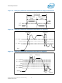
Figure 2-1.
Input Device Hysteresis
2.2.6
System Reference Clocks (BCLK{0/1}_DP,
BCLK{0/1}_DN)
The processor core, processor uncore, Intel® QuickPath Interconnect link, PCI Express*
and DDR3 memory interface frequencies are generated from BCLK{0/1}_DP and
BCLK{0/1}_DN signals. There is no relationship between core frequency and Intel®
QuickPath Interconnect link frequency. The processor maximum core frequency, Intel®
QuickPath Interconnect link frequency and DDR memory frequency are set during
manufacturing. It is possible to override the processor core frequency setting using
BIOS configuration software. This permits operation at frequencies lower than the
factory set maximum frequencies.
The processor core frequency is configured during reset by using values stored within
the device during manufacturing.
Clock multiplying within the processor is provided by the internal phase locked loop
(PLL), which requires a constant frequency BCLK{0/1}_DP, BCLK{0/1}_DN input, with
exceptions for spread spectrum clocking. DC specifications for the BCLK{0/1}_DP,
BCLK{0/1}_DN inputs are provided in Table 2-16.
Intel® Xeon® Processor E5-2400 v3 Product Family
Datasheet Volume One
16
Electrical Specifications
2.2.7
JTAG and Test Access Port (TAP) Signals
Due to the voltage levels supported by other components in the JTAG and Test Access
Port (TAP) logic, Intel recommends the processor be first in the TAP chain, followed by
any other components within the system. A translation buffer should be used to
connect to the rest of the chain unless one of the other components is capable of
accepting an input of the appropriate voltage. Two copies of each signal may be
required with each driving a different voltage level.
2.2.8
Processor Sideband Signals
The processor include asynchronous sideband signals that provide asynchronous input,
output or I/O signals between the processor and the platform or Platform Controller
Hub. Details can be found in Table 2-4 and the platform design guide.
All Processor Asynchronous Sideband input signals are required to be
asserted/deasserted for a defined number of BCLKs in order for the processor to
recognize the proper signal state.
2.2.9
Power, Ground and Sense Signals
Processors also include power and ground inputs and voltage sense points. Details can
be found in Table 2-4 and the Platform Design Guide.
2.2.9.1
Power and Ground Lands
All VCCIN, VCCD, ,VCCIO_IN and VCCPECI lands must be connected to their respective
processor power planes, while all VSS lands must be connected to the system ground
plane. Refer to the platform design guide for decoupling, voltage plane and routing
guidelines for each power supply voltage.
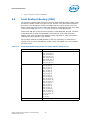
For clean on-chip power distribution, processors include lands for all required voltage
supplies. These are listed in Table 2-1.
Table 2-1.
Power and Ground Lands
Power and
Ground
Lands
Comments
VCCIN
107
Each VCCIN land must be connected to the voltage supply providing input to the
integrated voltage regulators. The operating voltage is requested via by the SVID
interface.
VCCD
16
Each VCCD land is connected to a switchable supply that provides power to the
processor DDR3 interface. This supply also powers the DDR3 memory subsystem.
VCCD is also controlled by the SVID Bus
VCCIO_IN
1
Connected to Miscellaneous I/O voltage supply.
VCCPECI
1
Connected to Miscellaneous I/O voltage supply.
VSS
2.2.9.2
Number of
Lands
417
Ground
Decoupling Guidelines
Due to its large number of transistors and high internal clock speeds, the processor is
capable of generating large current swings between low and full power states. This may
cause voltages on power planes to sag below their minimum values if bulk decoupling is
not adequate. Large electrolytic bulk capacitors (CBULK), help maintain the output
voltage during current transients, for example coming out of an idle condition. Care
Intel® Xeon® Processor E5-2400 v3 Product Family
Datasheet Volume One
17
Electrical Specifications
must be taken in the baseboard design to ensure that the voltages provided to the
processor remain within the specifications listed in Table 2-10. Failure to do so can
result in timing violations or reduced operational lifetime of the processor. For
requirements and implementation details, refer to the Platform Design Guide.
2.2.9.3
Voltage Identification (VID)
The target voltage level or the VID setting is transmitted via the SVID bus from the
processor to the voltage regulator controller chip. The VID settings are the nominal
voltages to be delivered to the processor's lands. VID codes will vary as a function of
temperature and current load changes in order to minimize power and maximize
performance of the processor. The processor specifies the VID required from the
voltage regulator to operate at desired frequencies.
Individual processor VID values may be calibrated during manufacturing such that two
processor units with the same core frequency may have different default VID settings.
If the processor socket is empty (SKTOCC_N high), or a “not supported” response is
received from the SVID bus, then the voltage regulation circuit cannot supply the
voltage that is requested, the voltage regulator must disable itself or not power on.
Vout MAX register (30h) is programmed by the processor to set the maximum
supported VID code and if the programmed VID code is higher than the VID supported
by the VR, then VR will respond with a “not supported” acknowledgement.
2.2.9.3.1
SVID Voltage Regulator Addressing
The processor addresses two voltage rail control segments (VCCIN and VCCD). The SVID
data packet contains a 4-bit address encoding as shown in Table 2-2
Table 2-2.
SVID Address Usage
PWM Address (HEX)
Processor Supply
00
VCCIN
01
NA
02
VCCD
03
N/A
Notes:
1.
Consult VR vendor for determining the physical address assignment method for their controllers.
2.
VR addressing is assigned on a per voltage rail basis.
3.
Dual VR controllers have two addresses with the lowest order address, always being the higher phase
count.
4.
For future platform flexibility, the VR controller should include an address offset, as shown with +1 not
used.
2.2.10
Reserved or Unused Signals
All Reserved (RSVD) signals must not be connected. Connection of these signals to
VCCIN, VCCD, VCCIO_IN, VCCPECI, VSS, or to any other signal (including each other) can result
in component malfunction or incompatibility with future processors.
For reliable operation, always connect unused inputs or bi-directional signals to an
appropriate signal level. Unused active high inputs should be connected through a
resistor to ground (VSS). Unused outputs maybe left unconnected; however, this may
interfere with some Test Access Port (TAP) functions, complicate debug probing, and
prevent boundary scan testing. A resistor must be used when tying bi-directional
signals to power or ground. When tying any signal to power or ground, a resistor will
Intel® Xeon® Processor E5-2400 v3 Product Family
Datasheet Volume One
18
Electrical Specifications
also allow for system testability. Resistor values should be within ± 20% of the
impedance of the baseboard trace, unless otherwise noted in the appropriate platform
design guidelines.
2.3
Signal Group Summary
Signals are grouped by buffer type and similar characteristics as listed in Table 2-3. The
buffer type indicates which signaling technology and specifications apply to the signals.
Table 2-3.
Signal Description Buffer Types
Buffer Type
Description
Analog
Analog reference or output. May be used as a threshold voltage or for buffer
compensation
Asynchronous1
Signal has no timing relationship with any system reference clock.
CMOS
CMOS buffers: 1.05V
DDR3
DDR3 buffers: 1.5V and 1.35V
DMI2
Direct Media Interface Gen 2 signals compatible with PCI Express* 2.0 and 1.0
Signaling Environment AC Specifications.
Intel® QPI
Current-mode 6.4 GT/s and 8.0 GT/s forwarded-clock Intel® QuickPath Interconnect
signaling
Open Drain CMOS
Open Drain CMOS (ODCMOS) buffers: 1.05V tolerant
PCI Express*
PCI Express* interface signals. These signals are compatible with PCI Express 3.0
Signalling Environment AC Specifications and are AC coupled. The buffers are not
3.3-V tolerant. Refer to the PCIe specification.
Reference
Voltage reference signal.
SSTL
Source Series Terminated Logic (JEDEC SSTL_15)
Notes:
1.
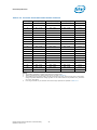
Table 2-4.
Qualifier for buffer type.
Signal Groups (Sheet 1 of 3)
Differential/Single
Ended
Signals1
Buffer Type
DDR3 Reference Clocks2
Differential
SSTL Output
DDR{1/2/3}_CLK_D[N/P][3:0]
DDR3 Command Signals2
Single ended
SSTL Output
DDR{1/2/3}_BA[2:0]
DDR{1/2/3}_CAS_N
DDR{1/2/3}_MA[15:0]
DDR{1/2/3}_PAR
DDR{1/2/3}_RAS_N
DDR{1/2/3}_WE_N
DDR3 Control Signals2
Single ended
CMOS1.5v Output
DDR{1/2/3}_CS_N[7:0]
DDR{1/2/3}_ODT[3:0]
DDR{1/2/3}_CKE[3:0]
Reference Output
DDR01_VREFDQ[1], DDR23_VREFDQ[1:0]
Reference Input
DDR01_VREF, DDR23_VREF
Compensation Input
DDR{01/23}_RCOMP[2:0]
DDR3 Data Signals2
Intel® Xeon® Processor E5-2400 v3 Product Family
Datasheet Volume One
19
Electrical Specifications
Table 2-4.
Signal Groups (Sheet 2 of 3)
Differential/Single
Ended
Signals1
Buffer Type
Differential
SSTL Input/Output
DDR{1/2/3}_DQS_[N/P][17:0]
Single ended
SSTL Input/Output
DDR{1/2/3}_DQ[63:0]
DDR{1/2/3}_ECC[7:0]
SSTL Input
DDR{1/2/3}_PAR_ERR_N
DDR3 Miscellaneous Signals2
Single ended
CMOS Input
Note: Input voltage from
cannot exceed 1.08V max.
DRAM_PWR_OK_C{01/23}
CMOS1.5v Output
DDR_RESET_C{1/23}_N
PCI Express* Port 1 & 3Signals
Differential
PCI Express* Input
PE1A_RX_D[N/P][3:0]
PE1B_RX_D[N/P][7:4]
PE3A_RX_D[N/P][3:0]
PE3B_RX_D[N/P][7:4]
PE3C_RX_D[N/P][11:8]
PE3D_RX_D[N/P][15:12]
Differential
PCI Express* Output
PE1A_TX_D[N/P][3:0]
PE1B_TX_D[N/P][7:4]
PE3A_TX_D[N/P][3:0]
PE3B_TX_D[N/P][7:4]
PE3C_TX_D[N/P][11:8]
PE3D_TX_D[N/P][15:12]
DMI2/PCI Express* Signals
Differential
DMI2 Input
DMI_RX_D[N/P][3:0]
DMI2 Output
DMI_TX_D[N/P][3:0]
Intel® QuickPath Interconnect (Intel® QPI) Signals
Differential
Intel® QPI Input
QPI1_DRX_D[N/P][19:0]
QPI1_CLKRX_D[N/P]
Intel® QPI Output
QPI1_DTX_D[N/P][19:0]
QPI1_CLKTX_D[N/P]
Platform Environmental Control Interface (PECI)
Single ended
PECI
PECI
System Reference Clock (BCLK{0/1})
Differential
CMOS1.05v Input
BCLK{0/1}_D[N/P]
Open Drain CMOS
Input/Output
DDR_SCL_C{01/23}
DDR_SDA_C{01/23}
PE_HP_SCL
PE_HP_SDA
SMBus
Single ended
Intel® Xeon® Processor E5-2400 v3 Product Family
Datasheet Volume One
20
Electrical Specifications
Table 2-4.
Signal Groups (Sheet 3 of 3)
Differential/Single
Ended
Signals1
Buffer Type
JTAG & TAP Signals
Single ended
CMOS1.05v Input
TCK, TDI, TMS, TRST_N, EAR_N
CMOS1.05v Input/Output
PREQ_N
CMOS1.05v Output
PRDY_N
Open Drain CMOS
Input/Output
BPM_N[7:0]
Open Drain CMOS Output
TDO
Serial VID Interface (SVID) Signals
Single ended
CMOS1.05v Input
SVIDALERT_N
Open Drain CMOS
Input/Output
SVIDDATA
Open Drain CMOS Output
SVIDCLK
Processor Asynchronous Sideband Signals
Single ended
CMOS1.05v Input
BIST_ENABLE
BMCINIT
DEBUG_EN_N
FRMAGENT
PWRGOOD
PMSYNC
RESET_N
SAFE_MODE_BOOT
SOCKET_ID[1:0]
TXT_AGENT
TXT_PLTEN
CMOS1.05v Output
FIVR_FAULT
Open Drain CMOS
Input/Output
CATERR_N
MEM_HOT_C{01/23}_N
MSMI_N
PM_FAST_WAKE_N
PROCHOT_N
Open Drain CMOS Output
ERROR_N[2:0]
THERMTRIP_N
Miscellaneous Signals
N/A
PROC_ID_N 2
SKTOCC_N
Output
Power/Other Signals
Power / Ground
VCCIN, VCCD,VCCIO_IN, VCCPECI, VSS
Sense Points
VCCIN_SENSE
VSS_VCCIN_SENSE
Notes:
1.
2.
DDR{1/2/3} refers toDDR3 Channel 1, DDR3 Channel 2 and DDR3 Channel 3.
PROC_ID_N land is unconnected within the processor package.
Intel® Xeon® Processor E5-2400 v3 Product Family
Datasheet Volume One
21
Electrical Specifications
Table 2-5.
Signals with On-Die Termination
Signal Name
Pull Up /Pull
Down
Rail
Value
Pull Up
VCCIO_IN
5K-15K
Ω
1
Pull Down
VSS
5K-15K
Ω
1
BIST_ENABLE
BMCINIT
Units
Notes
DDR{1/2/3}_PAR_ERR_N
Pull Up
VCCD
100
Ω
1
DEBUG_EN_N
Pull Up
VCCIO_IN
5K-15K
Ω
1
EAR_N
Pull Up
VCCIO_IN
5K-15K
Ω
1
Pull Down
VSS
5K-15K
Ω
1
PM_FAST_WAKE_N
Pull Up
VCCIO_IN
5K-15K
Ω
1
SAFE_MODE_BOOT
Pull Down
VSS
5K-15K
Ω
1
FRMAGENT
SOCKET_ID[1:0]
Pull Down
VSS
5K-15K
Ω
1
TCK
Pull Down
VSS
5K-15K
Ω
1
TDI
Pull Up
VCCIO_IN
5K-15K
Ω
1
TMS
Pull Up
VCCIO_IN
5K-15K
Ω
1
TRST_N
Pull Up
VCCIO_IN
5K-15K
Ω
1
TXT_AGENT
Pull Down
VSS
5K-15K
Ω
1
TXT_PLTEN
Pull Up
VCCIO_IN
5K-15K
Ω
1
Notes:
1.
Refer to the Platform Design Guide for circuit implementations for these signals.
2.4
Power-On Configuration (POC) Options
Functional options can be configured by hardware strapping of input signals. The
processor samples its hardware configuration at reset, on the active-to-inactive
transition of RESET_N, or upon assertion of PWRGOOD (inactive-to-active transition).
Configuration options are described in Table 2-6.
The sampled input configures the processor for subsequent operation. These
configuration options cannot be changed except by another reset transition of the
latching signal (RESET_N or PWRGOOD).
Table 2-6.
Power-On Configuration Option Lands
Configuration Option
Output high impedance state (FRB mode)
Execute BIST (Built-In Self Test)
Enable Service Processor Boot Mode
Enable Intel® Trusted Execution Technology (Intel® TXT) Platform
Power-up Sequence Halt
Enable Bootable Firmware Agent
Enable Intel® Trusted Execution Technology (Intel® TXT) Agent
Enable Safe Mode Boot
Configure Socket ID
Land Name
Notes
PROCHOT_N
1
BIST_ENABLE
2
BMCINIT
3
TXT_PLTEN
3
EAR_N
3
FRMAGENT
3
TXT_AGENT
3
SAFE_MODE_BOOT
3
SOCKET_ID[1:0]
3
Notes:
1.
PROCHOT_N for FRB mode is latched at de-assertion of RESET_N. Output high-impedance option enables
Fault Resilient Booting (FRB) as detailed in Section 2.5.
2.
BIST_ENABLE is sampled at de-assertion of RESET_N.
Intel® Xeon® Processor E5-2400 v3 Product Family
Datasheet Volume One
22
Electrical Specifications
3.
2.5
Signal is sampled at assertion of PWRGOOD .
Fault Resilient Booting (FRB)
The processor supports both socket and core level Fault Resilient Booting (FRB), which
provides the ability to boot the system as long as there is one processor functional in
the system. One limitation to socket level FRB is that the system cannot boot if the
legacy socket that connects to an active PCH becomes unavailable since this is the path
to the system BIOS. See Table 2-7 for a list of output tri-state FRB signals.
Socket level FRB will tri-state processor outputs via the PROCHOT_N signal. Assertion
of the PROCHOT_N signal through RESET_N de-assertion will tri-state processor
outputs. Note, that individual core disabling is also supported for those cases where
disabling the entire package is not desired.
The processor extends the FRB capability to the core granularity by maintaining a
register in the uncore so that BIOS or another entity can disable one or more specific
processor cores.
Table 2-7.
Fault Resilient Booting (Output Tri-State) Signals (Sheet 1 of 2)
Output Tri-State Signal Groups
Signals
Intel® QPI
QPI0_CLKTX_DN[1:0]
QPI0_CLKTX_DP[1:0]
QPI0_DTX_DN[19:0]
QPI0_DTX_DP[19:0]
QPI1_CLKTX_DN[1:0]
QPI1_CLKTX_DP[1:0]
QPI1_DTX_DN[19:0]
QPI1_DTX_DP[19:0]
PCI Express*
PE1A_TX_DN[3:0]
PE1A_TX_DP[3:0]
PE1B_TX_DN[7:4]
PE1B_TX_DP[7:4]
PE2A_TX_DN[3:0]
PE2A_TX_DP[3:0]
PE2B_TX_DN[7:4]
PE2B_TX_DP[7:4]
PE2C_TX_DN[11:8]
PE2C_TX_DP[11:8]
PE2D_TX_DN[15:12]
PE2D_TX_DP[15:12]
PE3A_TX_DN[3:0]
PE3A_TX_DP[3:0]
PE3B_TX_DN[7:4]
PE3B_TX_DP[7:4]
PE3C_TX_DN[11:8]
PE3C_TX_DP[11:8]
PE3D_TX_DN[15:12]
PE3D_TX_DP[15:12]
PE_HP_SCL
PE_HP_SDA
DMI2
DMI_TX_DN[3:0], DMI_TX_DP[3:0]
Intel® Xeon® Processor E5-2400 v3 Product Family
Datasheet Volume One
23
Electrical Specifications
Table 2-7.
2.6
Fault Resilient Booting (Output Tri-State) Signals (Sheet 2 of 2)
Output Tri-State Signal Groups
Signals
SMBus
DDR_SCL_C01
DDR_SDA_C01
DDR_SCL_C23
DDR_SDA_C23
PE_HP_SCL
PE_HP_SDA
Processor Sideband
BPM_N[7:0]
CATERR_N
ERROR_N[2:0]
FIVR_FAULT
MEM_HOT_C01_N
MEM_HOT_C23_N
MSMI_N
PM_FAST_WAKE_N
PROCHOT_N
PECI
PM_FASTWAKE_N
PRDY_N
THERMTRIP_N
SVID
SVIDCLK
SVIDDATA
Mixing Processors
Intel® supports and validates two-processor configurations only in which all processors
operate with the same Intel® QuickPath Interconnect frequency, core frequency, power
segment having the same internal cache sizes. Mixing components operating at
different internal clock frequencies is not supported and will not be validated by Intel®.
Combining processors from different power segments is also not supported.
Note:
Processors within a system must operate at the same frequency per bits [15:8] of the
FLEX_RATIO MSR (Address: 194h); however this does not apply to frequency
transitions initiated due to thermal events, Extended HALT, Enhanced Intel® SpeedStep
Technology transitions signal.
Not all operating systems can support dual processors with mixed frequencies. Mixing
processors of different steppings but the same model (as per CPUID instruction) is
supported provided there is no more than one stepping delta between the processors,
for example, S and S+1.
S and S+1 is defined as mixing of two CPU steppings in the same platform where one
CPU is S (stepping) = CPUID.(EAX=01h):EAX[3:0], and the other is S+1 =
CPUID.(EAX=01h):EAX[3:0]+1. The stepping ID is found in EAX[3:0] after executing
the CPUID instruction with Function 01h. Details regarding the CPUID instruction are
provided in Intel® 64 and IA-32 Architectures Software Developer’s Manual (SDM)
Volumes 1, 2, and 3.
2.7
Flexible Motherboard Guidelines (FMB)
Flexible Motherboard (FMB) guidelines are estimates of the maximum values the
processor will have over certain time periods. The values are only estimates and actual
specifications for future processors may differ. Processors may or may not have
Intel® Xeon® Processor E5-2400 v3 Product Family
Datasheet Volume One
24
Electrical Specifications
specifications equal to the FMB value in the foreseeable future. System designers
should meet the FMB values to ensure their systems will be compatible with future
processors.
2.8
Absolute Maximum and Minimum Ratings
Table 2-8 specifies absolute maximum and minimum ratings. At conditions outside
functional operation condition limits, but within absolute maximum and minimum
ratings, neither functionality nor long-term reliability can be expected. If a device is
returned to conditions within functional operation limits after having been subjected to
conditions outside these limits, but within the absolute maximum and minimum
ratings, the device may be functional, but with its lifetime degraded depending on
exposure to conditions exceeding the functional operation condition limits.
Although the processor contains protective circuitry to resist damage from ElectroStatic Discharge (ESD), precautions should always be taken to avoid high static
voltages or electric fields.
Table 2-8.
Processor Absolute Minimum and Maximum Ratings
Symbol
Parameter
Min
Max
Unit
VCCIN
Integrated Voltage Regulator voltage with respect to VSS
-0.3
1.98
V
VCCD
Processor I/O supply voltage for DDR3 (standard voltage) with
respect to VSS
-0.3
1.85
V
VCCDL
Processor I/O supply voltage for DDR3L (Low Voltage) with
respect to VSS
-0.3
1.7
V
VCCIO_IN
Processor I/O voltage with respect to VSS
-0.3
1.4
V
VCCPECI
Processor PECI voltage with respect to VSS
-0.3
1.4
V
Notes:
1.
For functional operation, all processor electrical, signal quality, mechanical, and thermal specifications must
be satisfied.
2.
Overshoot and undershoot voltage guidelines for input, output, and I/O signals are outlined. Excessive
overshoot or undershoot on any signal will likely result in permanent damage to the processor.
2.8.1
Storage Condition Specifications
Environmental storage condition limits define the temperature and relative humidity
limits to which the device is exposed to while being stored in a Moisture Barrier Bag.
The specified storage conditions are for component level prior to board attach (see
notes in Table 2-9 for post board attach limits).
Table 2-9 specifies absolute maximum and minimum storage temperature limits which
represent the maximum or minimum device condition beyond which damage, latent or
otherwise, may occur. The table also specifies sustained storage temperature, relative
humidity, and time-duration limits. These limits specify the maximum or minimum
device storage conditions for a sustained period of time. At conditions outside sustained
limits, but within absolute maximum and minimum ratings, quality & reliability may be
affected.
Table 2-9.
Storage Condition Ratings (Sheet 1 of 2)
Symbol
Tabsolute storage
Parameter
Min
Max
Unit
The minimum/maximum device storage temperature beyond
which damage (latent or otherwise) may occur when
subjected to for any length of time.
-25
125
°C
Intel® Xeon® Processor E5-2400 v3 Product Family
Datasheet Volume One
25
Electrical Specifications
Table 2-9.
Storage Condition Ratings (Sheet 2 of 2)
Symbol
Parameter
Min
Max
Unit
Tsustained storage
The minimum/maximum device storage temperature for a
sustained period of time.
-5
40
°C
Tshort term storage
The ambient storage temperature (in shipping media) for a
short period of time.
-20
85
°C
RHsustained storage
The maximum device storage relative humidity for a
sustained period of time.
60% @ 24
°C
Timesustained
storage
A prolonged or extended period of time; typically associated
with sustained storage conditions Unopened bag, includes 6
months storage time by customer.
0
30
months
Timeshort term
storage
A short period of time (in shipping media).
0
72
hours
Notes:
1.
Storage conditions are applicable to storage environments only. In this scenario, the processor must not
receive a clock, and no lands can be connected to a voltage bias. Storage within these limits will not affect
the long-term reliability of the device. For functional operation, refer to the processor case temperature
specifications.
2.
These ratings apply to the Intel® component and do not include the tray or packaging.
3.
Failure to adhere to this specification can affect the long-term reliability of the processor.
4.
Non-operating storage limits post board attach: Storage condition limits for the component once attached
to the application board are not specified. Intel® does not conduct component level certification
assessments post board attach given the multitude of attach methods, socket types and board types used
by customers. Provided as general guidance only, Intel® board products are specified and certified to meet
the following temperature and humidity limits (Non-Operating Temperature Limit: -40C to 70C & Humidity:
50% to 90%, non condensing with a maximum wet bulb of 28C).
5.
Device storage temperature qualification methods follow JEDEC High and Low Temperature Storage Life
Standards: JESD22-A119 (low temperature) and JESD22-A103 (high temperature).
2.9
DC Specifications
DC specifications are defined at the processor pads, unless otherwise noted.
DC specifications are only valid while meeting specifications for case temperature, clock
frequency, and input voltages. Care should be taken to read all notes associated with
each specification.
2.9.1
Voltage and Current Specifications
Table 2-10. Voltage Specification
Symbol
Parameter
Voltage
Plane
Min
Nom
Max
1.47
1.8
1.85
Unit
Notes1
V
2, 3
mV
10
VCCIN
Input supply to Integrated Voltage Regulator
VCCIN
VID_STEP
VID step size for VR12.5
VCCIN
VCCD
VCCD
(Standard)
I/O Voltage for DDR3
(Standard Voltage)
VCCD
1.425
1.50
1.575
V
VCCDL
(Low)
I/O Voltage for DDR3L
(Low Voltage)
VCCD
1.283
1.35
1.451
V
VCCIO_IN
I/O Voltage
VCCIO_IN
1.0
1.05
1.10
V
3, 5, 9
VCCPECI
PECI Voltage
VCCPECI
1.0
1.05
1.10
V
3, 5, 9
10
Notes:
1.
Unless otherwise noted, all specifications in this table apply to all processors in this processor family. Specifications are based
on preliminary silicon characterization.
Intel® Xeon® Processor E5-2400 v3 Product Family
Datasheet Volume One
26
Electrical Specifications
2.
Individual processor VID values may be calibrated during manufacturing such that two devices at the same speed may have
different settings.
3.
Voltages are targets only. A variable voltage source should exist on systems in the event that a different voltage is required.
A future processor may be developed requiring a nominal voltage 0.95V.
4.
The VCCIN voltage specification requirements are measured across the remote sense pin pairs (VCCIN_SENSE and
VSS_VCCIN_SENSE) on the processor package. Voltage measurement should be taken with a DC to 100 MHz bandwidth
oscilloscope limit (or DC to 20 MHz for older model oscilloscopes), using a 1.5 pF maximum probe capacitance, and 1 MΩ
minimum impedance. The maximum length of the ground wire on the probe should be less than 5 mm to ensure external
noise from the system is not coupled in the scope probe.
5.
For the processor refer to Table 2-12 and corresponding Figure 2-2. The processor should not be subjected to any static VCCIN
level that exceeds the VCCIN_MAX associated with any particular current. Failure to adhere to this specification can shorten
processor lifetime.
6.
Minimum VCCIN and maximum ICCIN are specified at the maximum processor case temperature (TCASE) shown in the
processor TMSDG. ICCIN_MAX is specified at the relative VCCIN_MAX point on the VCCIN Loadline. The processor is capable of
drawing ICCIN_MAX for up to 4 milliseconds.
7.
This specification represents the VCCIN increase or decrease due to each VID transition
8.
Baseboard bandwidth is limited to 20 MHz.
9.
DC + AC + Ripple specification
10. VCCIN has a VBOOT setting of 1.7 V and is included in the PWRGOOD indication.
Table 2-11. Processor Power Supply Current Specifications
Parameter and Definition
ICCIO_IN
I/O Termination Supply,
Processor Current on VCCIO_IN, VCCPECI
ICCD 3
Memory Controller DDR3 Supply,
Processor Current on VCCD
ICCIN
Integrated Voltage Regulator Supply
Processor Current on VCCIN
TDC 2
(A)
Max
(A)
.02
0.1
5
7
LV70W-10C
43
90
138
LV65W-8C 1S
40
83
128
LV55W-8C
34
70
109
LV50W-6C
28
57
88
LV45W-4C
25
51
78
Processor TDP / Core count
PMAX5
(W)
Notes1
All Intel® Xeon® Processor E5-2400
v3 Product Family
3
Notes:
1.
Unless otherwise noted, all specifications in this table apply to all models in the processor family. Specifications are based on
preliminary silicon characterization.
2.
TDC (Thermal Design Current) is the sustained (DC equivalent) current that the processor is capable of drawing indefinitely
and should be used for the voltage regulator thermal assessment. The voltage regulator is responsible for monitoring its
temperature and asserting the necessary signal to inform the processor of a thermal excursion.
3.
ICCD specifications are current draw on VCCD of processor only and do not include current consumption by memory devices.
4.
Minimum VCCIN and maximum ICCIN are specified at the maximum processor case temperature (TCASE) ICCIN_MAX is
specified at the corresponding voltage point on the VCCIN Loadline. The processor is capable of drawing ICCIN_MAX for up to
4 milliseconds.
5.
PMAX is provided for VCCIN for ensuring adequate capability in design and sizing of the power delivery components.
2.9.2
VCCIN Power Delivery for Integrated Voltage Regulators
The VCCIN voltage rail supplies the input source to the integrated voltage regulators
powering cores, cache and system agents. This integration improves regulation of ondie voltages optimizing performance and power savings. The VCCIN rail is supplied by
an external voltage regulator.
Adhering to power delivery specifications is mandatory for ensuring long-term reliable
operation of processors and system components. The Intel® Xeon® Processor E5-2400
v3 Product Family implements a 1.40-mΩ loadline with a tolerance band ±25 mV.
Static and Transient Tolerances are repeated here for convenience in Table 2-12 and
Figure 2-2
Intel® Xeon® Processor E5-2400 v3 Product Family
Datasheet Volume One
27
Electrical Specifications
Table 2-12. Processor VCCIN Static and Transient Tolerance
ICCIN [A]
VCCIN_Max [V]
VCCIN_Nominal [V]
VCCIN_Min [V]
Notes
0
VID + 0.025
VID - 0.000
VID - 0.025
1,2,3,4
5
VID + 0.018
VID - 0.007
VID - 0.032
1,2,3,4
10
VID + 0.011
VID - 0.014
VID - 0.039
1,2,3,4
15
VID +0.004
VID - 0.021
VID - 0.046
1,2,3,4
20
VID - 0.003
VID - 0.028
VID - 0.053
1,2,3,4
25
VID - 0.010
VID - 0.035
VID - 0.060
1,2,3,4
30
VID - 0.017
VID - 0.042
VID - 0.067
1,2,3,4
35
VID - 0.024
VID - 0.049
VID - 0.074
1,2,3,4
40
VID - 0.031
VID - 0.056
VID - 0.081
1,2,3,4
45
VID - 0.038
VID - 0.063
VID - 0.088
1,2,3,4
50
VID - 0.045
VID - 0.070
VID - 0.095
1,2,3,4
55
VID - 0.052
VID - 0.077
VID - 0.102
1,2,3,4
60
VID - 0.059
VID - 0.084
VID - 0.109
1,2,3,4
65
VID - 0.066
VID - 0.091
VID - 0.116
1,2,3,4
70
VID - 0.073
VID - 0.098
VID - 0.123
1,2,3,4
75
VID - 0.080
VID - 0.105
VID - 0.130
1,2,3,4
80
VID - 0.087
VID - 0.112
VID - 0.137
1,2,3,4
85
VID - 0.094
VID - 0.119
VID - 0.144
1,2,3,4
90
VID - 0.101
VID - 0.126
VID - 0.151
1,2,3,4
95
VID - 0.108
VID - 0.133
VID - 0.158
1,2,3,4
100
VID - 0.115
VID - 0.140
VID - 0.165
1,2,3,4
Notes:
1.
The loadline specification includes both static and transient limits.
2.
Table is intended to aid in reading discrete points on graph in Figure 2-2.
3.
The Loadlines specify voltage limits at the die measured at the Vccin_sense and Vss_Vccin_sense lands.
Voltage regulation feedback for voltage regulator circuits must be taken from processor Vccin_sense and
Vss_Vccin_sense lands.
4.
ICCIN range extends only to maximum value of the target processor as specified in Table 2-11.
Intel® Xeon® Processor E5-2400 v3 Product Family
Datasheet Volume One
28
Electrical Specifications
Figure 2-2.
VCCIN Static and Transient Tolerance Loadlines
2.9.3
Die Voltage Validation
VCCIN overshoot events at the processor must meet the specifications in Table 2-13
when measured across the VCCIN_SENSE and VSS_VCCIN_SENSE lands. Overshoot
events that are < 10 ns in duration may be ignored. These measurements of processor
die level overshoot should be taken with a 100 MHz bandwidth limited oscilloscope.
2.9.3.1
VCCIN Overshoot Specifications
The processor can tolerate short transient overshoot events where VCCIN exceeds the
VID voltage when transitioning from a high-to-low current load condition. This
overshoot cannot exceed VID + VOS_MAX (VOS_MAX is the maximum allowable overshoot
above VID). These specifications apply to the processor die voltage as measured across
the VCCIN_SENSE and VSS_VCCIN_SENSE lands.
Table 2-13. VCCIN Overshoot Specifications
Symbol
Parameter
Max
Units
Figure
VOS_MAX
Magnitude of VCCIN overshoot above VID
75
mV
2-3
TOS_MAX
Time duration of VCCIN overshoot above VCCIN_MAX value at the new
lighter load
25
μs
2-3
Intel® Xeon® Processor E5-2400 v3 Product Family
Datasheet Volume One
29
Notes
Electrical Specifications
Figure 2-3.
VCCIN Overshoot Example Waveform
Notes:
1.
VOS_MAX is the measured overshoot voltage.
2.
TOS_MAX is the measured time duration above VCCIN_MAX(I1).
3.
Istep: Load Release Current Step, for example, I2 to I1, where I2 > I1.
4.
VCCIN_MAX(I1) = VID + TOB
2.9.4
Signal DC Specifications
DC specifications are defined at the processor pads, unless otherwise noted.
DC specifications are only valid while meeting specifications for case temperature
specified in the processor TMSDG, clock frequency, and input voltages. Care should be
taken to read all notes associated with each specification.
Table 2-14. DDR3 and DDR3L Signal DC Specifications (Sheet 1 of 2)
Symbol
IIL
Parameter
Min
Input Leakage Current
Nom
-1.4
Max
Units
Notes1
+1.4
mA
10
0.43*VCCD
V
2, 3
V
2, 4, 5
Data Signals
VIL
Input Low Voltage
VIH
Input High Voltage
RON
DDR3 Data Buffer On Resistance
21
31
Ω
6
Data ODT
On-Die Termination for Data Signals
45
90
55
110
Ω
8
PAR_ERR_N ODT
On-Die Termination for Parity Error
Signals
0.57*VCCD
100
Ω
Reference Clock Signals, Command, and Data Signals
VOL
Output Low Voltage
(VCCD / 2) * (RON /(RON+RVTT_TERM))
V
2, 7
VOH
Output High Voltage
VCCD - ((VCCD / 2)* (RON/(RON+RVTT_TERM))
V
2, 5, 7
Reference Clock Signal
Intel® Xeon® Processor E5-2400 v3 Product Family
Datasheet Volume One
30
Electrical Specifications
Table 2-14. DDR3 and DDR3L Signal DC Specifications (Sheet 2 of 2)
Symbol
Parameter
Min
DDR3 Clock Buffer On Resistance
RON
Nom
Max
Units
Notes1
31
Ω
6
21
Command Signals
RON
DDR3 Command Buffer On Resistance
16
24
Ω
6
RON
DDR3 Reset Buffer On Resistance
25
75
Ω
6
VOL_CMOS1.5v
Output Low Voltage
DDR_RESET_ C{01/23}_N
0.2*VCCD
V
1,2
VOH_CMOS1.5v
Output High Voltage
DDR_RESET_ C{01/23}_N
V
1,2
IIL_CMOS1.5v
Input Leakage Current
μA
1,2
0.9*VCCD
-100
+100
Control Signals
RON
DDR3 Control Buffer On Resistance
DDR01_RCOMP[0]
COMP Resistance
21
128.7
130
31
Ω
6
131.3
Ω
9,12
DDR01_RCOMP[1]
COMP Resistance
39.8
40.2
40.6
Ω
9,12
DDR01_RCOMP[2]
COMP Resistance
119.8
121
122.2
Ω
9,12
DDR23_RCOMP[0]
COMP Resistance
128.7
130
131.3
Ω
9,12
DDR23_RCOMP[1]
COMP Resistance
39.8
40.2
40.6
Ω
9,12
DDR23_RCOMP[2]
COMP Resistance
119.8
121
122.2
Ω
9,12
0.55*VCCD +
0.2
V
2, 3,
11, 13
V
2, 4, 5,
11, 13
DDR3 Miscellaneous Signals
VIL
Input Low Voltage
DRAM_PWR_OK_C{01/23}
VIH
Input High Voltage
DRAM_PWR_OK_C{01/23}
0.55*VCCD +
0.3
Notes:
1.
Unless otherwise noted, all specifications in this table apply to all processor frequencies.
2.
The voltage rail VCCD which will be set to 1.50 V or 1.35 V nominal depending on the voltage of all DIMMs connected to the
processor.
3.
VIL is the maximum voltage level at a receiving agent that will be interpreted as a logical low value.
4.
VIH is the minimum voltage level at a receiving agent that will be interpreted as a logical high value.
5.
VIH and VOH may experience excursions above VCCD. However, input signal drivers must comply with the signal quality
specifications.
6.
This is the pull down driver resistance. Refer to processor signal integrity models for I/V characteristics. Reset drive does not
have a termination.
7.
RVTT_TERM is the termination on the DIMM and not controlled by the processor. Refer to the applicable DIMM datasheet.
8.
The minimum and maximum values for these signals are programmable by BIOS to one of the pairs.
9.
COMP resistance must be provided on the system board with 1% resistors. See the Platform Design Guide for implementation
details. DDR01_RCOMP[2:0] and DDR23_RCOMP[2:0] resistors are terminated to VSS.
10. Input leakage current is specified for all DDR3 signals.
11. DRAM_PWR_OK_C{01/23} must have a maximum of 30 ns rise or fall time over VCCD * 0.55 +300 mV and -200 mV and the
edge must be monotonic.
12. The DDR{01/23}_RCOMP error tolerance is ±15% from the compensated value.
13. DRAM_PWR_OK_C{01/23}: Data Scrambling must be enabled for production environments. Disabling Data scrambling is
supported only for debug and testing purposes. Operation of systems with Data Scrambling disabled violates specification.
Table 2-15. PECI DC Specifications (Sheet 1 of 2)
Symbol
Definition and Conditions
Min
Max
Units
-0.150
VCCPECI +0.150
V
Figure
Notes1
VIn
Input Voltage Range
VHysteresis
Hysteresis
0.100 * VCCPECI
VN
Negative-edge threshold voltage
0.275 * VCCPECI
0.500 * VCCPECI
V
2-1
2
VP
Positive-edge threshold voltage
0.550 * VCCPECI
0.725 * VCCPEC
V
2-1
2
Intel® Xeon® Processor E5-2400 v3 Product Family
Datasheet Volume One
31
V
Electrical Specifications
Table 2-15. PECI DC Specifications (Sheet 2 of 2)
Symbol
Definition and Conditions
Min
Max
Units
ISOURCE
High level output source
VOH = 0.75 * VCCPECI
-6.0
ILeak+
High impedance state leakage to VCCPECI (Vleak =
VOL)
50
200
µA
RON
Buffer On Resistance
20
36
Ω
CBus
Bus capacitance per node
VNoise
Signal noise immunity above 300 MHz
0.100 * VCCPECI
Output Edge Rate
(50 ohm to VSS, between VIL and VIH)
1.5
Figure
Notes1
mA
10
3
pF
4,5
Vp-p
4
V/ns
Notes:
1.
VCCPECI supplies the PECI interface. PECI behavior does not affect VCCPECI min/max specification
2.
It is expected that the PECI driver will take into account, the variance in the receiver input thresholds and consequently, be
able to drive its output within safe limits (-0.150 V to 0.275*VCCPECI for the low level and 0.725*VCCPECI to VCCPECI+0.150 V
for the high level).
3.
The leakage specification applies to powered devices on the PECI bus.
4.
One node is counted for each client and one node for the system host. Extended trace lengths might appear as additional
nodes.
5.
Excessive capacitive loading on the PECI line may slow down the signal rise/fall times and consequently limit the maximum bit
rate at which the interface can operate.
Table 2-16. System Reference Clock (BCLK{0/1}) DC Specifications
Symbol
Parameter
Min
VBCLK_diff_ih
Input High Voltage
(Differential)
VBCLK_diff_il
Input Low Voltage
(Differential)
Vcross (abs)
Absolute Crossing Point
(Single Ended)
Vcross(rel)
Relative Crossing Point
(Single Ended)
ΔVcross
Range of Crossing Points
(Single Ended)
VTH
Threshold Voltage
(Single Ended)
IIL
Input Leakage Current
Cpad
Pad Capacitance
Max
Notes1
Unit
Figure
V
2-7
-0.150
V
2-7
0.25
0.55
V
2-4
2-8
2, 4, 7
0.25 +0.5*(VHavg - 0.7)
0.55 + 0.5*(VHavg - 0.7)
V
2-4
3, 4, 5
V
2-9
6
0.150
0.140
Vcross - 0.1
1.12
Vcross + 0.1
V
1.50
μA
1.70
pF
8
Notes:
1.
Specifications apply to all processor frequencies. Parameters are specified at the processor pad.
2.
Crossing Voltage is defined as the instantaneous voltage value when the rising edge of BCLK{0/1}_DN is equal to the falling
edge of BCLK{0/1}_DP.
3.
VHavg is the statistical average of the VH measured by the oscilloscope.
4.
The crossing point must meet the absolute and relative crossing point specifications simultaneously.
5.
VHavg can be measured directly using “Vtop” on Agilent* and “High” on Tektronix oscilloscopes.
6.
VCROSS is defined as the total variation of all crossing voltages as defined in Note 3.
7.
The rising edge of BCLK{0/1}_DN is equal to the falling edge of BCLK{0/1}_DP.
8.
For Vin between 0 and Vih.
Table 2-17. SMBus DC Specifications (Sheet 1 of 2)
Symbol
Parameter
Min
Max
Units
0.3*VCCIO_IN
V
VIL
Input Low Voltage
VIH
Input High Voltage
0.7*VCCIO_IN
V
VHysteresis
Hysteresis
0.1*VCCIO_IN
V
Intel® Xeon® Processor E5-2400 v3 Product Family
Datasheet Volume One
32
Notes
Electrical Specifications
Table 2-17. SMBus DC Specifications (Sheet 2 of 2)
Symbol
Parameter
VOL
Output Low Voltage
RON
Buffer On Resistance
IL
Min
Units
0.2*VCCIO_IN
V
4
14
Ω
50
200
μA
0.05
0.6
V/ns
Leakage Current
Output Edge Rate (50 ohm to VCCIO_IN, between VIL and VIH)
Max
Notes
Table 2-18. JTAG and TAP Signals DC Specifications
Symbol
Parameter
VIL
Input Low Voltage
VIH
Input High Voltage
VIL
Input Low Voltage: TCK
VIH
Input High Voltage: TCK
VOL
Output Low Voltage
VHysteresis
Hysteresis
RON
Buffer On Resistance
BPM_N[7:0], PRDY_N, TDO
IIL
Input Leakage Current
Min
Max
Units
0.4*VCCIO_IN
V
0.8*VCCIO_IN
V
0.4*VCCIO_IN
0.6*VCCIO_IN
Output Edge Rate (50 ohm to VCCIO_IN)
BPM_N[7:0], PRDY_N, TDO
V
V
0.2*VCCIO_IN
V
4
14
Ω
50
200
μA
0.1*VCCIO_IN
Input Edge Rate
BPM_N[7:0], EAR_N, PREQ_N, TCK, TDI, TMS, TRST_N
V
0.05
0.2
1.5
V/ns
1, 2
V/ns
1
Note:
1.
Measured between VIL and VIH.
2.
Edge rate must be met or the signal must transition monotonically to the asserted state.
Table 2-19. Serial VID Interface (SVID) DC Specifications
Symbol
Parameter
VIL
Input Low Voltage
SVIDDATA, SVIDALERT_N
VIH
Input High Voltage
SVIDDATA, SVIDALERT_N
VOL
Output Low Voltage
SVIDCLK, SVIDDATA
VHysteresis
Hysteresis
RON
Buffer On Resistance
SVIDCLK, SVIDDATA
IIL
Input Leakage Current
Min
Nom
Max
Units
Notes
0.4*VCCIO_IN
V
1
V
1
V
1
V
1
Ω
2
0.7*VCCIO_IN
0.2*VCCIO_IN
0.05*VCCIO_IN
4
14
50
200
Input Edge Rate
SVIDALERT_N
0.05
Output Edge Rate
(50 ohm to VCCIO_IN)
0.20
1.5
μA
3,4
V/ns
5, 6
V/ns
5
Notes:
1.
VCCIO_IN refers to instantaneous VCCIO_IN.
2.
Measured at 0.31*VCCIO_IN
3.
Vin between 0V and VCCIO_IN
4.
Refer to the Platform Design Guide for routing design guidelines.
5.
These are measured between VIL and VIH.
6.
The signal edge rate must be met or the signal must transition monotonically to the asserted state.
Intel® Xeon® Processor E5-2400 v3 Product Family
Datasheet Volume One
33
Notes
Electrical Specifications
Table 2-20. Processor Asynchronous Sideband DC Specifications
Symbol
Parameter
Min
Max
Units
Notes
0.4*VCCIO_IN
V
1,2
V
1,2
200
μA
1,2
CMOS1.05v Signals
VIL_CMOS1.05v
Input Low Voltage
VIH_CMOS1.05v
Input High Voltage
IIL_CMOS1.05v
Input Leakage Current
0.6*VCCIO_IN
50
Open Drain CMOS (ODCMOS) Signals
VIL_ODCMOS
Input Low Voltage
MEM_HOT_C{01/23}_N, PROCHOT_N
0.3*VCCIO_IN
V
1,2
VIL_ODCMOS
Input Low Voltage
CATERR_N, MSMI_N, PM_FAST_WAKE_N
0.4*VCCIO_IN
V
1,2
VIH_ODCMOS
Input High Voltage
V
1,2
VOL_ODCMOS
Output Low Voltage
VHysteresis
Hysteresis
MEM_HOT_{C01/23}_N, PROCHOT_N
VHysteresis
Hysteresis
CATERR_N, MSMI_N, PM_FAST_WAKE_N
ILeak
Input Leakage Current
RON
Buffer On Resistance
0.7*VCCIO_IN
V
1,2
0.1*VCCIO_IN
0.2*VCCIO_IN
V
1,2
0.05*VCCIO_IN
V
1,2
50
200
μA
4
14
Ω
1,2
Output Edge Rate
MEM_HOT_C{01/23}_N, ERROR_N[2:0],
THERMTRIP, PROCHOT_N
0.05
0.60
V/ns
3
Output Edge Rate
CATERR_N, MSMI_N, PM_FAST_WAKE_N
0.2
1.5
V/ns
3
Notes:
1.
This table applies to the processor sideband and miscellaneous signals specified in Table 2-4.
2.
Unless otherwise noted, all specifications in this table apply to all processor frequencies.
3.
These signals are measured between VIL and VIH.
Table 2-21. Miscellaneous Signals DC Specifications
Symbol
Parameter
Min
Typical
Max
Units
1.80
V
Notes
PROC_ID_N
VO_ABS_MAX
Output Absolute Max Voltage
IO
Output Current
N/A
VO_ABS_MAX
Output Absolute Max Voltage
3.30
IOMAX
Output Max Current
1, 2
1, 2
SKTOCC_N
3.50
V
1
1
mA
1
Notes:
1.
For specific routing guidelines, see the Platform Design Guide for details.
2.
PROC_ID_N land is unconnected within the package.
2.9.4.1
PCI Express* DC Specifications
The processor DC specifications for the PCI Express* are available in the PCI Express
Base Specification - Revision 3.0. This document will provide only the processor
exceptions to the PCI Express Base Specification - Revision 3.0.
Intel® Xeon® Processor E5-2400 v3 Product Family
Datasheet Volume One
34
Electrical Specifications
2.9.4.2
DMI2/PCI Express* DC Specifications
The processor DC specifications for the DMI2/PCI Express* are available in the PCI
Express Base Specification 2.0 and 1.0. This document will provide only the processor
exceptions to the PCI Express Base Specification 2.0 and 1.0.
2.9.4.3
Intel® QuickPath Interconnect DC Specifications
Intel® QuickPath Interconnect specifications are defined at the processor lands. Refer
to the Platform Design Guide for specific implementation details. In most cases,
termination resistors are not required as these are integrated into the processor silicon.
The processor DC specifications for the Intel® QPI interface are available in the Intel®
QuickPath Interconnect V1.1 Base Electrical Specification and Validation Methodologies.
This document will provide only the processor exceptions to the Intel® QuickPath
Interconnect V1.1 Base Electrical Specification and Validation Methodologies.
2.9.4.4
Reset and Miscellaneous Signal DC Specifications
For a power-on Reset, RESET_N must stay active for at least 3.5 millisecond after VCCIN
and BCLK{0/1} have reached their proper specifications. RESET_N must not be kept
asserted for more than 100 ms while PWRGOOD is asserted. RESET_N must be held
asserted for at least 3.5 millisecond before it is deasserted again. RESET_N must be
held asserted before PWRGOOD is asserted. This signal does not have on-die
termination and must be terminated on the system board.
2.10
System Reference Clock (BCLK{0/1}) Waveforms
Figure 2-4.
BCLK{0/1} Differential Clock Crosspoint Specification
650
Crossing Point (mV)
600
550
550 mV
500
450
550 + 0.5 (VHavg - 700)
400
250 + 0.5 (VHavg - 700)
350
300
250
250 mV
200
660 670 680 690 700 710 720 730 740 750 760 770 780 790 800 810 820 830 840 850
VHavg (mV)
Intel® Xeon® Processor E5-2400 v3 Product Family
Datasheet Volume One
35
Electrical Specifications
Figure 2-5.
BCLK{0/1} Differential Clock Measurement Points for Duty Cycle and Period
Clock Period
(Differential)
Positive Duty
Cycle
(Differential)
Negative Duty
Cycle
(Differential)
0.0V
BCLK
Figure 2-6.
BCLK{0/1} Differential Clock Measurement Points for Edge Rate
Rise Edge Rate
Fall Edge Rate
VIH = +150 mV
0.0V
VIL = -150 mV
BCLK
Figure 2-7.
BCLK{0/1} Differential Clock Measurement Point for Ringback
T STABLE
VRB-Differential
VIH = +150 mV
VRB = +100 mV
0.0V
VRB = -100 mV
VIL = -150 mV
REFCLK +
Intel® Xeon® Processor E5-2400 v3 Product Family
Datasheet Volume One
T STABLE
36
VRB-Differential
Electrical Specifications
Figure 2-8.
BCLK{0/1} Single Ended Clock Measurement Points for Absolute Cross Point
and Swing
VMAX = 1.40V
BCLK_DN
VCROSS MAX = 550mV
VCROSS MIN = 250mV
BCLK_DP
VMIN = -0.30V
Figure 2-9.
BCLK{0/1} Single Ended Clock Measurement Points for Delta Cross Point
BCLK_DN
VCROSS DELTA = 140 mV
BCLK_DP
2.11
Signal Quality
Data transfer requires the clean reception of data signals and clock signals. Ringing
below receiver thresholds, non-monotonic signal edges, and excessive voltage swings
will adversely affect system timings. Ringback and signal non-monotonicity cannot be
tolerated since these phenomena may inadvertently advance receiver state machines.
Excessive signal swings (overshoot and undershoot) are detrimental to silicon gate
oxide integrity, and can cause device failure if absolute voltage limits are exceeded.
Overshoot and undershoot can also cause timing degradation due to the build up of
inter-symbol interference (ISI) effects.
For these reasons, it is crucial that the designer work towards a solution that provides
acceptable signal quality across all systematic variations encountered in volume
manufacturing.
This section documents signal quality metrics used to derive topology and routing
guidelines through simulation. All specifications are specified at the processor die (pad
measurements).
Specifications for signal quality are for measurements at the processor core only and
are only observable through simulation. Therefore, proper simulation is the only way to
verify proper timing and signal quality.
Intel® Xeon® Processor E5-2400 v3 Product Family
Datasheet Volume One
37
Electrical Specifications
2.11.1
DDR3 Signal Quality Specifications
Various scenarios for the DDR3 Signals have been simulated to generate a set of layout
guidelines which are available in the Platform Design Guide.
Overshoot (or undershoot) is the absolute value of the maximum voltage above or
below VSS. The overshoot/undershoot specifications limit transitions beyond specified
maximum voltages or VSS due to the fast signal edge rates. The processor can be
damaged by single and/or repeated overshoot or undershoot events on any input,
output, or I/O buffer if the charge is large enough (i.e., if the over/undershoot is great
enough). Baseboard designs which meet signal integrity and timing requirements and
which do not exceed the maximum overshoot or undershoot limits listed in Table 2-22
will insure reliable IO performance for the lifetime of the processor.
2.11.2
I/O Signal Quality Specifications
Signal Quality specifications for PCIe Signals are included as part of the PCIe DC
specifications and PCIe AC specifications. Various scenarios have been simulated to
generate a set of layout guidelines which are available in the Platform Design Guide.
2.11.3
Intel® QuickPath Interconnect Signal Quality
Specifications
Signal Quality specifications for Differential Intel® QuickPath Interconnect Signals are
included as part of the Intel® QuickPath Interconnect defined in the Intel® QuickPath
Interconnect V1.1 Base Electrical Specification and Validation Methodologies. Various
scenarios have been simulated to generate a set of layout guidelines which are
available in the Platform Design Guide.
2.11.4
Input Reference Clock Signal Quality Specifications
Overshoot/Undershoot and Ringback specifications for BCLK{0/1}_D[N/P] are found in
Table 2-22. Overshoot/Undershoot and Ringback specifications for the DDR3 Reference
Clocks are specified by the DIMM.
2.11.5
Overshoot/Undershoot Tolerance
Overshoot (or undershoot) is the absolute value of the maximum voltage above or
below VSS, see Figure 2-10. The overshoot/undershoot specifications limit transitions
beyond VCCD or VSS due to the fast signal edge rates. The processor can be damaged
by single and/or repeated overshoot or undershoot events on any input, output, or I/O
buffer if the charge is large enough (that is, if the over/undershoot is great enough).
Determining the impact of an overshoot/undershoot condition requires knowledge of
the magnitude, the pulse direction, and the activity factor (AF). Permanent damage to
the processor is the likely result of excessive overshoot/undershoot.
Baseboard designs which meet signal integrity and timing requirements and which do
not exceed the maximum overshoot or undershoot limits listed in Table 2-22 will insure
reliable IO performance for the lifetime of the processor.
Table 2-22. Processor I/O Overshoot/Undershoot Specifications (Sheet 1 of 2)
Signal Group
Intel® QuickPath Interconnect
Minimum
Undershoot
Maximum
Overshoot
Overshoot
Duration
Undershoot
Duration
Notes
-0.2 * VCCIO_IN
1.2 * VCCIO_IN
39 ps
15 ps
1,2
Intel® Xeon® Processor E5-2400 v3 Product Family
Datasheet Volume One
38
Electrical Specifications
Table 2-22. Processor I/O Overshoot/Undershoot Specifications (Sheet 2 of 2)
Signal Group
DDR3
Minimum
Undershoot
Maximum
Overshoot
Overshoot
Duration
Undershoot
Duration
Notes
-0.2 * VCCD
1.2 * VCCD
0.25*TCH
0.1*TCH
1,2,3
-0.3V
1.15V
N/A
N/A
1,2
-0.42V
VCCIO_IN + 0.28
1.25 ns
0.5 ns
4
System Reference Clock (BCLK{0/1})
PWRGOOD Signal
Notes:
1.
These specifications are measured at the processor pad.
2.
Refer to Figure 2-10 for description of allowable Overshoot/Undershoot magnitude and duration.
3.
TCH is the minimum high pulse width duration.
4.
For PWRGOOD DC specifications see Table 2-20.
2.11.5.1
Overshoot/Undershoot Magnitude
Overshoot/Undershoot magnitude describes the maximum potential difference between
a signal and its voltage reference level. For the processor, both overshoot and
undershoot magnitude are referenced to VSS. It is important to note that the overshoot
and undershoot conditions are separate and their impact must be determined
independently.
The pulse magnitude and duration, and activity factor must be used to determine if the
overshoot/undershoot pulse is within specifications.
2.11.5.2
Overshoot/Undershoot Pulse Duration
Overshoot/undershoot pulse duration describes the total amount of time that an
overshoot/undershoot event exceeds the overshoot/undershoot reference voltage. The
total time could encompass several oscillations above the reference voltage. Multiple
overshoot/undershoot pulses within a single overshoot/undershoot event may need to
be measured to determine the total pulse duration.
Note:
Oscillations below the reference voltage cannot be subtracted from the total
overshoot/undershoot pulse duration.
2.11.5.3
Activity Factor
Activity factor (AF) describes the frequency of overshoot (or undershoot) occurrence
relative to a clock. Since the highest frequency of assertion of any common clock signal
is every other clock, an AF = 0.1 indicates that the specific overshoot (or undershoot)
waveform occurs every other clock cycle.
The specification provided in the table shows the maximum pulse duration allowed for a
given overshoot/undershoot magnitude at a specific activity factor. Each table entry is
independent of all others, meaning that the pulse duration reflects the existence of
overshoot/undershoot events of that magnitude ONLY. A platform with an
overshoot/undershoot that just meets the pulse duration for a specific magnitude
where the AF < 0.1, means that there can be no other overshoot/undershoot events,
even of lesser magnitude (note that if AF = 0.1, then the event occurs at all times and
no other events can occur).
Intel® Xeon® Processor E5-2400 v3 Product Family
Datasheet Volume One
39
Electrical Specifications
2.11.5.4
Reading Overshoot/Undershoot Specification Tables
The overshoot/undershoot specification for the processor is not a simple single value.
Instead, many factors are needed to determine the over/undershoot specification. In
addition to the magnitude of the overshoot, the following parameters must also be
known: the width of the overshoot and the activity factor (AF). To determine the
allowed overshoot for a particular overshoot event, the following must be done:
1. Determine the signal group a particular signal falls into.
2. Determine the magnitude of the overshoot or the undershoot (relative to VSS).
3. Determine the activity factor (How often does this overshoot occur?).
4. Next, from the appropriate specification table, determine the maximum pulse
duration (in nanoseconds) allowed.
5. Compare the specified maximum pulse duration to the signal being measured. If
the pulse duration measured is less than the pulse duration shown in the table,
then the signal meets the specifications.
Undershoot events must be analyzed separately from overshoot events as they are
mutually exclusive.
2.11.5.5
Compliance to Overshoot/Undershoot Specifications
The overshoot/undershoot specifications listed in the table specify the allowable
overshoot/undershoot for a single overshoot/undershoot event. However, most
systems will have multiple overshoot and/or undershoot events that each have their
own set of parameters (duration, AF and magnitude). While each overshoot on its own
may meet the overshoot specification, when you add the total impact of all overshoot
events, the system may fail. A guideline to ensure a system passes the overshoot and
undershoot specifications is shown below.
1. If only one overshoot/undershoot event magnitude occurs, ensure it meets the
over/undershoot specifications in the following tables, OR
2. If multiple overshoots and/or multiple undershoots occur, measure the worst case
pulse duration for each magnitude and compare the results against the AF = 0.1
specifications. If all of these worst case overshoot or undershoot events meet the
specifications (measured time < specifications) in the table (where AF= 0.1), then
the system passes.
Table 2-23. Processor Sideband Signal Group Overshoot/Undershoot Tolerance
Absolute Maximum Overshoot
(V)
Absolute Maximum Undershoot
(V)
Pulse Duration (ns)
AF=0.1
Pulse Duration (ns)
AF=0.01
1.3335 V
0.2835 V
3 ns
5 ns
1.2600 V
0.210 V
5 ns
5 ns
Intel® Xeon® Processor E5-2400 v3 Product Family
Datasheet Volume One
40
Electrical Specifications
Figure 2-10. Maximum Acceptable Overshoot/Undershoot Waveform
Over Shoot
Over Shoot
Duration
Under Shoot
Duration
VSS
Under Shoot
Intel® Xeon® Processor E5-2400 v3 Product Family
Datasheet Volume One
41
Electrical Specifications
2.12
C-State Power
Table 2-24 lists the package level C-State power specifications for each processor
SKUs.
This represents the total power dissipated by the processor component in each C-State.
Table 2-24. Processor Package C-State Power Specifications
Processor TDP / Core count 1
C1E (W) 3
C3 (W) 3
C6 (W) 2
35
28
13
LV70W-10C
LV65W-8C 1S
30
24
13
LV55W-8C
30
24
12
LV50W-6C
27
23
12
LV45W-4C
27
23
12
Notes:
1.
SKUs are subject to change. Contact your Intel Field Representative to obtain the latest SKU information.
2.
Package C6 power specified at Tcase = 50°C.
3.
C1E and C3 power values are characterized not tested.
§
Intel® Xeon® Processor E5-2400 v3 Product Family
Datasheet Volume One
42
Signal Descriptions
3
Signal Descriptions
This chapter describes the processor signals. They are arranged in functional groups
according to their associated interface or category.
3.1
System Memory Interface Signals
Table 3-1.
Memory Channel DDR1, DDR2, DDR3
Signal Name
DDR{1/2/3}_BA[2:0]
Description
Bank Address. Defines the bank which is the destination for the current
Activate, Read, Write, or Precharge command.
DDR{1/2/3}_CAS_N
Column Address Strobe.
DDR{1/2/3}_CKE[3:0]
Clock Enable.
DDR{1/2/3}_CLK_DN[3:0]
DDR{1/2/3}_CLK_DP[3:0]
Differential clocks to the DIMM. All command and control signals are valid on
the rising edge of clock.
DDR{1/2/3}_CS_N[7:0]
Chip Select. Each signal selects one rank as the target of the command and
address.
DDR{1/2/3}_DQ[63:0]
Data Bus. DDR3 Data bits.
DDR{1/2/3}_DQS_P[17:0]
DDR{1/2/3}_DQS_N[17:0]
Data strobes. Differential pair, Data/ECC Strobe. Differential strobes latch
data/ECC for each DRAM. Different numbers of strobes are used depending on
whether the connected DRAMs are x4,x8. Driven with edges in center of data,
receive edges are aligned with data edges.
DDR{1/2/3}_ECC[7:0]
Check bits. An error correction code is driven along with data on these lines for
DIMMs that support that capability
DDR{1/2/3}_MA[15:0]
Memory Address. Selects the Row address for Reads and writes, and the
column address for activates. Also used to set values for DRAM configuration
registers.
DDR{1/2/3}_PAR
Odd parity across Address and Command.
DDR{1/2/3}_ODT[3:0]
On Die Termination. Enables DRAM on die termination during Data Write or
Data Read transactions.
DDR{1/2/3}_PAR_ERR_N
Parity Error detected by Registered DIMM (one for each channel).
DDR{1/2/3}_RAS_N
Row Address Strobe.
DDR{1/2/3}_WE_N
Write Enable.
Intel® Xeon® Processor E5-2400 v3 Product Family
Datasheet Volume One
43
Signal Descriptions
Table 3-2.
Memory Channel Miscellaneous
Signal Name
Description
DDR_RESET_C01_N
DDR_RESET_C23_N
System memory reset: Reset signal from processor to DRAM devices on the
DIMMs. DDR_RESET_C01_N is used for memory channel1 while
DDR_RESET_C23_N is used for memory channels 2 and 3.
DDR_SCL_C01
DDR_SCL_C23
SMBus clock for the dedicated interface to the serial presence detect (SPD) and
thermal sensors (TSoD) on the DIMMs. DDR_SCL_C01 is used for memory
channel1 while DDR_SCL_C23 is used for memory channels 2 and 3.
DDR_SDA_C01
DDR_SDA_C23
SMBus data for the dedicated interface to the serial presence detect (SPD) and
thermal sensors (TSoD) on the DIMMs. DDR_SDA_C01 is used for memory
channel1 while DDR_SDA_C23 is used for memory channels 2 and 3.
DDR01_VREF
DDR23_VREF
Voltage reference for system memory reads. DDR01_VREF is used for memory
channel1 while DDR23_VREF is shared by memory channels 2 and 3.
DDR01_VREFDQ[1]
DDR23_VREFDQ[1:0]
Voltage reference for system memory writes. DDR01_VREFDQ[1] is used for
memory channel1. DDR23_VREFDQ[0] is used for channel 2 and
DDR23_VREFDQ[1] for channel 3. These signal levels are adjusted by MRC to
optimize timing margins.
DDR{01/23}_RCOMP[2:0]
System memory impedance compensation. Impedance compensation must be
terminated on the system board using a precision resistor. See the Platform
Design Guide for implementation details.
DRAM_PWR_OK_C01
DRAM_PWR_OK_C23
Power good input signal used to indicate that the VCCD power supply is stable
for memory channel 1 and channels 2 & 3.
3.2
PCI Express* Based Interface Signals
Note:
PCI Express* Ports 1and 3 Signals are receive and transmit differential pairs.
Table 3-3.
PCI Express* Port 1 Signals
Signal Name
Table 3-4.
Description
PE1A_RX_DN[3:0]
PE1A_RX_DP[3:0]
PCIe Receive Data Input
PE1B_RX_DN[7:4]
PE1B_RX_DP[7:4]
PCIe Receive Data Input
PE1A_TX_DN[3:0]
PE1A_TX_DP[3:0]
PCIe Transmit Data Output
PE1B_TX_DN[7:4]
PE1B_TX_DP[7:4]
PCIe Transmit Data Output
PCI Express* Port 3 Signals (Sheet 1 of 2)
Signal Name
Description
PE3A_RX_DN[3:0]
PE3A_RX_DP[3:0]
PCIe Receive Data Input
PE3B_RX_DN[7:4]
PE3B_RX_DP[7:4]
PCIe Receive Data Input
PE3C_RX_DN[11:8]
PE3C_RX_DP[11:8]
PCIe Receive Data Input
PE3D_RX_DN[15:12]
PE3D_RX_DP[15:12]
PCIe Receive Data Input
PE3A_TX_DN[3:0]
PE3A_TX_DP[3:0]
PCIe Transmit Data Output
Intel® Xeon® Processor E5-2400 v3 Product Family
Datasheet Volume One
44
Signal Descriptions
Table 3-4.
PCI Express* Port 3 Signals (Sheet 2 of 2)
Signal Name
Table 3-5.
Description
PE3B_TX_DN[7:4]
PE3B_TX_DP[7:4]
PCIe Transmit Data Output
PE3C_TX_DN[11:8]
PE3C_TX_DP[11:8]
PCIe Transmit Data Output
PE3D_TX_DN[15:12]
PE3D_TX_DP[15:12]
PCIe Transmit Data Output
PCI Express* Miscellaneous Signals
Signal Name
Description
PE_HP_SCL
PCI Express* Hot-Plug SMBus Clock: Provides PCI Express* hot-plug support
via a dedicated SMBus interface. Requires an external general purpose
input/output (GPIO) expansion device on the platform.
PE_HP_SDA
PCI Express* Hot-Plug SMBus Data: Provides PCI Express* hot-plug support via
a dedicated SMBus interface. Requires an external general purpose
input/output (GPIO) expansion device on the platform.
Note:
Refer to the Platform Design Guide for additional implementation details.
3.3
DMI2/PCI Express* Port 0 Signals
Table 3-6.
DMI2 and PCI Express Port 0 Signals
Signal Name
Description
DMI_RX_DN[3:0]
DMI_RX_DP[3:0]
DMI2 Receive Data Input
DMI_TX_DP[3:0]
DMI_TX_DN[3:0]
DMI2 Transmit Data Output
3.4
Intel® QuickPath Interconnect Signals
Table 3-7.
Intel® QPI Port Signals
Signal Name
Description
QPI1_CLKRX_DN/DP
Reference Clock Differential Input. These pins provide the PLL reference clock
differential input. The Intel® QPI forward clock frequency is half the Intel® QPI
data rate.
QPI1_CLKTX_DN/DP
Reference Clock Differential Output. These pins provide the PLL reference clock
differential input. The Intel® QPI forward clock frequency is half the Intel® QPI
data rate.
QPI1_DRX_DN/DP[19:0]
Intel® QPI Receive data input.
QPI1_DTX_DN/DP[19:0]
Intel® QPI Transmit data output.
Intel® Xeon® Processor E5-2400 v3 Product Family
Datasheet Volume One
45
Signal Descriptions
3.5
PECI Signal
Table 3-8.
PECI Signal
Signal Name
PECI
Description
PECI (Platform Environment Control Interface) is the serial sideband interface to the
processor and is used primarily for thermal, power and error management. Details
regarding the PECI electrical specifications, protocols and functions can be found in the
Platform Environment Control Interface Specification.
3.6
System Reference Clock Signals
Table 3-9.
System Reference Clock (BCLK) Signals
3.7
Signal Name
Description
BCLK{0/1}_D[N/P]
Reference Clock Differential input. These pins provide the PLL reference clock
differential input into the processor. 100 MHz typical BCLK0 is the Intel® QPI reference
clock (system clock) and BCLK1 is the PCI Express* reference clock.
JTAG and TAP Signals
Table 3-10. JTAG and TAP Signals
Signal Name
BPM_N[7:0]
Breakpoint and Performance Monitor Signals: I/O signals from the processor that
indicate the status of breakpoints and programmable counters used for monitoring
processor performance. These are 100 MHz signals.
EAR_N
External Alignment of Reset, used to bring the processor up into a deterministic state.
This signal is pulled up on the die, refer to Table 2-5 for details.
PRDY_N
Probe Mode Ready is a processor output used by debug tools to determine processor
debug readiness.
PREQ_N
Probe Mode Request is used by debug tools to request debug operation of the processor.
TCK
TCK (Test Clock) provides the clock input for the processor Test Bus (also known as the
Test Access Port).
TDI
TDI (Test Data In) transfers serial test data into the processor. TDI provides the serial
input needed for JTAG specification support.
TDO
TDO (Test Data Out) transfers serial test data out of the processor. TDO provides the
serial output needed for JTAG specification support.
TMS
TMS (Test Mode Select) is a JTAG specification support signal used by debug tools.
TRST_N
TRST_N (Test Reset) resets the Test Access Port (TAP) logic. TRST_N must be driven
low during power-on reset.
Note:
3.8
Description
Refer to the Platform Design Guide for Debug Port implementation details.
Serial VID Interface (SVID) Signals
Table 3-11. SVID Signals (Sheet 1 of 2)
Signal Name
SVIDALERT_N
Description
Serial VID alert.
Intel® Xeon® Processor E5-2400 v3 Product Family
Datasheet Volume One
46
Signal Descriptions
Table 3-11. SVID Signals (Sheet 2 of 2)
Signal Name
3.9
Description
SVIDCLK
Serial VID clock.
SVIDDATA
Serial VID data out.
Processor Asynchronous Sideband and
Miscellaneous Signals
Table 3-12. Processor Asynchronous Sideband Signals (Sheet 1 of 3)
Signal Name
Description
BIST_ENABLE
BIST Enable Strap. Input which allows the platform to enable or disable built-in self test
(BIST) on the processor. This signal is pulled up on the die, refer to Table 2-5 for details.
BMCINIT
BMC Initialization Strap. Indicates whether Service Processor Boot Mode should be
used. Used in combination with FRMAGENT and SOCKET_ID inputs.
• 0: Service Processor Boot Mode Disabled. Example boot modes: Local PCH (this
processor hosts a legacy PCH with firmware behind it), Intel® QPI Link Boot (for
processors one hop away from the FW agent), or Intel® QPI Link Init (for
processors more than one hop away from the firmware agent).
• 1: Service Processor Boot Mode Enabled. In this mode of operation, the processor
performs the absolute minimum internal configuration and then waits for the
Service Processor to complete its initialization. The socket boots after receiving a
“GO” handshake signal via a firmware scratchpad register.
This signal is pulled down on the die, refer to Table 2-5 for details.
CATERR_N
Indicates that the system has experienced a fatal or catastrophic error and cannot
continue to operate. The processor will assert CATERR_N for nonrecoverable machine
check errors and other internal unrecoverable errors. It is expected that every
processor in the system will wire-OR CATERR_N for all processors. Since this is an I/O
land, external agents are allowed to assert this land which will cause the processor to
take a machine check exception. This signal is sampled after PWRGOOD assertion.
On the processor, CATERR_N is used for signaling the following types of errors:
• Legacy MCERR’s, CATERR_N is asserted for 16 BCLKs.
• Legacy IERR’s, CATERR_N remains asserted until warm or cold reset.
DEBUG_EN_N
Forces debug to be enabled. This allows debug to occur beginning from cold boot.
ERROR_N[2:0]
Error status signals for integrated I/O (IIO) unit:
• 0 = Hardware correctable error (no operating system or firmware action necessary)
• 1 = Non-fatal error (operating system or firmware action required to contain and
recover)
• 2 = Fatal error (system reset likely required to recover)
FIVR_FAULT
Indicates an internal error has occurred with the integrated voltage regulator. The
FIVR_FAULT signal can be sampled any time after 1.5 ms after the assertion of
PWRGOOD. FIVR_FAULT must be qualified by THERMTRIP_N assertion. See the Platform
Design Guide for proper connectivity.
FRMAGENT
Bootable Firmware Agent Strap. This input configuration strap used in combination with
SOCKET_ID to determine whether the socket is a legacy socket, bootable firmware
agent is present, and DMI links are used in PCIe* mode (instead of DMI2 mode).
The firmware flash ROM is located behind the local PCH attached to the processor via
the DMI2 interface.This signal is pulled down on the die, refer to Table 2-5 for details.
Intel® Xeon® Processor E5-2400 v3 Product Family
Datasheet Volume One
47
Signal Descriptions
Table 3-12. Processor Asynchronous Sideband Signals (Sheet 2 of 3)
Signal Name
MEM_HOT_C01_N
MEM_HOT_C23_N
Description
Memory throttle control. MEM_HOT_C01_N and MEM_HOT_C23_N signals have two
modes of operation – input and output mode.
Input mode is externally asserted and is used to detect external events such as
VR_HOT# from the memory voltage regulator and causes the processor to throttle the
appropriate memory channels.
Output mode is asserted by the processor known as level mode. In level mode, the
output indicates that a particular branch of memory subsystem is hot.
MEM_HOT_C01_N is used for memory channel 1 while MEM_HOT_C23_N is used for
memory channels 2 & 3.
MSMI_N
Machine Check Exception (MCE) is signaled via this pin when eMCA2 is enabled.
PM_FAST_WAKE_N
Power Management Fast Wake. Enables quick package C3 - C6 exits of all sockets.
Asserted if any socket detects a break from package C3 - C6 state requiring all sockets
to exit the low power state to service a snoop, memory access, or interrupt. Expected to
be wired-OR among all processor sockets within the platform.
PMSYNC
Power Management Sync. A sideband signal to communicate power management status
from the Platform Controller Hub (PCH) to the processor.
PROCHOT_N
PROCHOT_N will go active when the processor temperature monitoring sensor detects
that the processor has reached its maximum safe operating temperature. This indicates
that the processor Thermal Control Circuit has been activated, if enabled. This signal
can also be driven to the processor to activate the Thermal Control Circuit. This signal is
sampled after PWRGOOD assertion.
If PROCHOT_N is asserted at the deassertion of RESET_N, the processor will tristate its
outputs.
PWRGOOD
Power Good is a processor input. The processor requires this signal to be a clean
indication that BCLK and power supplies are stable and within their specifications.
“Clean” implies that the signal will remain low (capable of sinking leakage current),
without glitches, from the time that the power supplies are turned on until they come
within specification. The signal must then transition monotonically to a high state.
PWRGOOD can be driven inactive at any time, but clocks and power must again be
stable before a subsequent rising edge of PWRGOOD. PWRGOOD transitions from
inactive to active when all supplies except VCCIN are stable. VCCIN has a VBOOT of 1.7 V
volts and is included in PWRGOOD indication in this phase. However, for the active to
inactive transition, if any CPU power supply is about to fail or is out of regulation, the
PWRGOOD is to be negated.
The signal must be supplied to the processor; it is used to protect internal circuits
against voltage sequencing issues. It should be driven high throughout boundary scan
operation.
RESET_N
Asserting the RESET_N signal resets the processor to a known state and invalidates its
internal caches without writing back any of their contents. Note some PLL, Intel®
QuickPath Interconnect and error states are not affected by reset and only PWRGOOD
forces them to a known state.
RSVD
RESERVED. All signals that are RSVD must be left unconnected on the board. Refer to
Section 2.2.10, “Reserved or Unused Signals” for details.
SAFE_MODE_BOOT
Safe mode boot Strap. SAFE_MODE_BOOT allows the processor to wake up safely by
disabling all clock gating, this allows BIOS to load registers or patches if required. This
signal is sampled after PWRGOOD assertion. The signal is pulled down on the die, refer
to Table 2-5 for details.
SOCKET_ID[1:0]
Socket ID Strap. Socket identification configuration straps for establishing the PECI
address, Intel® QPI Node ID, and other settings. This signal is used in combination with
FRMAGENT to determine whether the socket is a legacy socket, bootable firmware
agent is present, and DMI links are used in PCIe* mode (instead of DMI2 mode). Each
processor socket consumes one Node ID, and there are 128 Home Agent tracker
entries. This signal is pulled down on the die, refer to Table 2-5 for details.
TEST[4:0]
Test[4:0] must be individually connected to an appropriate power source or ground
through a resistor for proper processor operation.
Intel® Xeon® Processor E5-2400 v3 Product Family
Datasheet Volume One
48
Signal Descriptions
Table 3-12. Processor Asynchronous Sideband Signals (Sheet 3 of 3)
Signal Name
Description
THERMTRIP_N
Assertion of THERMTRIP_N (Thermal Trip) indicates one of two possible critical overtemperature conditions: One, the processor junction temperature has reached a level
beyond which permanent silicon damage may occur and Two, the system memory
interface has exceeded a critical temperature limit set by BIOS. Measurement of the
processor junction temperature is accomplished through multiple internal thermal
sensors that are monitored by the Digital Thermal Sensor (DTS). Simultaneously, the
Power Control Unit (PCU) monitors external memory temperatures via the dedicated
SMBus interface to the DIMMs. If any of the DIMMs exceed the BIOS defined limits, the
PCU will signal THERMTRIP_N to prevent damage to the DIMMs. Once activated, the
processor will stop all execution and shut down all PLLs. To further protect the
processor, all power supply voltages must be removed following the assertion of
THERMTRIP_N. Once activated, THERMTRIP_N remains latched until RESET_N is
asserted. While the assertion of the RESET_N signal may de-assert THERMTRIP_N, if
the processor's junction temperature remains at or above the trip level, THERMTRIP_N
will again be asserted after RESET_N is de-asserted. This signal can also be asserted if
the system memory interface has exceeded a critical temperature limit set by BIOS.
This signal is sampled after PWRGOOD assertion.
TXT_AGENT
Intel® Trusted Execution Technology (Intel® TXT) Agent Strap.
0 = Default. The socket is not the Intel® TXT Agent.
1 = The socket is the Intel® TXT Agent.
The legacy socket (identified by SOCKET_ID[1:0] = 00b) with Intel® TXT Agent should
always set the TXT_AGENT to 1b.
This signal is pulled down on the die, refer to Table 2-5 for details.
TXT_PLTEN
Intel® Trusted Execution Technology (Intel® TXT) Platform Enable Strap.
0 = The platform is not Intel® TXT enabled. All sockets should be set to zero.
1 = Default. The platform is Intel® TXT enabled. All sockets should be set to one. When
this is set, Intel® TXT functionality requires user to explicitly enable Intel® TXT via
BIOS setup.
This signal is pulled up on the die, refer to Table 2-5 for details.
Table 3-13. Miscellaneous Signals
Signal Name
Description
PROC_ID_N
This output can be used by the platform to distinguish between Intel® Xeon® Processor
E5-2400 v3 Product Family or a potential future product family. There is no connection
either to the silicon or package substrate.
SKTOCC_N
SKTOCC_N (Socket occupied) is used to indicate that a processor is present. This is
pulled to ground on the processor package; there is no connection to the processor
silicon for this signal.
DBR_N
ITP_BCLK_D[N/P]
JTAG_TDOX
These signals are pass-through pins with no connection to processor silicon for use with
Top Side Probe only. Signals pass from the system board through package substrate to
connector pins on the top side of the processor package. Top Side Probe implementation
is found in the Platform Design Guide.
SYS_PWROK
3.10
Processor Power and Ground Supplies
Table 3-14. Power and Ground Signals (Sheet 1 of 2)
Signal Name
VCCIN
Description
Power supply input for the Integrated Voltage Regulators the deliver power to processor
cores, lowest level caches, ring interface, and home agent. The output voltage of this
supply is selected by the processor, using the serial voltage identification (SVID)
interface.
Intel® Xeon® Processor E5-2400 v3 Product Family
Datasheet Volume One
49
Signal Descriptions
Table 3-14. Power and Ground Signals (Sheet 2 of 2)
Signal Name
Description
VCCIN_SENSE
VSS_VCCIN_SENSE
Isolated, low impedance connection to the processor power and ground. These signals
must be connected to the voltage regulator feedback circuit, which ensures processor
voltage remains within specification.
VCCIO_IN
Power supply for miscellaneous I/O interfaces of the processor.
VCCPECI
Power supply for PECI interface of the processor.
VCCD
Variable power supply for the processor system memory interface. Provided by one
regulator per CPU socket for all memory channels. The valid nominal voltage of this
supply (1.50V or 1.35V) is configured by BIOS after determining the operating voltages
of the installed memory.
Note:
VSS
The processor must be provided VCCD for proper operation, even in
configurations where no memory is populated.
Processor ground node.
§
Intel® Xeon® Processor E5-2400 v3 Product Family
Datasheet Volume One
50
Processor Land Listing
4
Processor Land Listing
4.1
Land Listing by Name
Note:
Table 4-1.
This land listing is provided in this document for convenience.
Table 4-1.
Land Listing (Sheet 2 of 37)
Land Listing (Sheet 1 of 37)
Land Name
Land
Number
Land Name
Buffer Type Direction
Land
Number
Buffer Type Direction
BCLK0_DN
AN13
CMOS
I
DDR1_CKE[0]
J25
SSTL
O
BCLK0_DP
AP13
CMOS
I
DDR1_CKE[1]
J26
SSTL
O
BCLK1_DN
AM30
CMOS
I
DDR1_CKE[2]
K24
SSTL
O
BCLK1_DP
AN30
CMOS
I
DDR1_CKE[3]
H26
SSTL
O
BIST_ENABLE
AM6
CMOS
I
DDR1_CLK_DN[0]
J17
SSTL
O
BMCINIT
AF1
CMOS
I
DDR1_CLK_DN[1]
G19
SSTL
O
L16
SSTL
O
BPM_N[0]
AL10
ODCMOS
I/O
DDR1_CLK_DN[2]
BPM_N[1]
AK15
ODCMOS
I/O
DDR1_CLK_DN[3]
H18
SSTL
O
BPM_N[2]
AR11
ODCMOS
I/O
DDR1_CLK_DP[0]
K17
SSTL
O
BPM_N[3]
AN11
ODCMOS
I/O
DDR1_CLK_DP[1]
H19
SSTL
O
BPM_N[4]
AP10
ODCMOS
I/O
DDR1_CLK_DP[2]
L17
SSTL
O
BPM_N[5]
AP11
ODCMOS
I/O
DDR1_CLK_DP[3]
J18
SSTL
O
K15
SSTL
O
BPM_N[6]
AN10
ODCMOS
I/O
DDR1_CS_N[0]
BPM_N[7]
AP12
ODCMOS
I/O
DDR1_CS_N[1]
L15
SSTL
O
CATERR_N
AT6
ODCMOS
I/O
DDR1_CS_N[2]
L11
SSTL
O
DBR_N
AE36
DDR1_CS_N[3]
K11
SSTL
O
DDR_RESET_C01_N
L26
CMOS
O
DDR1_CS_N[4]
J15
SSTL
O
DDR_RESET_C23_N
D27
CMOS
O
DDR1_CS_N[5]
L14
SSTL
O
DDR_SCL_C01
W7
ODCMOS
I/O
DDR1_CS_N[6]
L12
SSTL
O
DDR_SCL_C23
V40
ODCMOS
I/O
DDR1_CS_N[7]
K12
SSTL
O
AC34
SSTL
I/O
DDR_SDA_C01
W6
ODCMOS
I/O
DDR1_DQ[0]
DDR_SDA_C23
V37
ODCMOS
I/O
DDR1_DQ[1]
AC35
SSTL
I/O
DDR01_RCOMP[0]
P10
ANALOG
I
DDR1_DQ[10]
M35
SSTL
I/O
DDR01_RCOMP[1]
N10
ANALOG
I
DDR1_DQ[11]
M36
SSTL
I/O
DDR01_RCOMP[2]
W10
ANALOG
I
DDR1_DQ[12]
U35
SSTL
I/O
DDR01_VREF
M7
DC
O
DDR1_DQ[13]
U36
SSTL
I/O
DDR01_VREFDQ[1]
W4
DC
O
DDR1_DQ[14]
N35
SSTL
I/O
DDR1_BA[0]
H16
SSTL
O
DDR1_DQ[15]
N36
SSTL
I/O
J36
SSTL
I/O
DDR1_BA[1]
J16
SSTL
O
DDR1_DQ[16]
DDR1_BA[2]
J22
SSTL
O
DDR1_DQ[17]
J35
SSTL
I/O
DDR1_CAS_N
L13
SSTL
O
DDR1_DQ[18]
E35
SSTL
I/O
Intel® Xeon® Processor E5-2400 v3 Product Family
Datasheet Volume One
51
Processor Land Listing
Table 4-1.
Land Listing (Sheet 3 of 37)
Land Name
Land
Number
Table 4-1.
Buffer Type Direction
Land Listing (Sheet 4 of 37)
Land Name
Land
Number
Buffer Type Direction
DDR1_DQ[19]
F35
SSTL
I/O
DDR1_DQ[52]
Y9
SSTL
I/O
DDR1_DQ[2]
W35
SSTL
I/O
DDR1_DQ[53]
Y8
SSTL
I/O
DDR1_DQ[20]
K36
SSTL
I/O
DDR1_DQ[54]
AD9
SSTL
I/O
DDR1_DQ[21]
K35
SSTL
I/O
DDR1_DQ[55]
AD8
SSTL
I/O
DDR1_DQ[22]
E36
SSTL
I/O
DDR1_DQ[56]
Y1
SSTL
I/O
DDR1_DQ[23]
F36
SSTL
I/O
DDR1_DQ[57]
AA3
SSTL
I/O
DDR1_DQ[24]
L32
SSTL
I/O
DDR1_DQ[58]
AE1
SSTL
I/O
DDR1_DQ[25]
K32
SSTL
I/O
DDR1_DQ[59]
AE2
SSTL
I/O
DDR1_DQ[26]
L28
SSTL
I/O
DDR1_DQ[6]
Y35
SSTL
I/O
DDR1_DQ[27]
K28
SSTL
I/O
DDR1_DQ[60]
Y3
SSTL
I/O
DDR1_DQ[28]
K33
SSTL
I/O
DDR1_DQ[61]
Y2
SSTL
I/O
DDR1_DQ[29]
L33
SSTL
I/O
DDR1_DQ[62]
AD2
SSTL
I/O
DDR1_DQ[3]
W36
SSTL
I/O
DDR1_DQ[63]
AD3
SSTL
I/O
DDR1_DQ[30]
L29
SSTL
I/O
DDR1_DQ[7]
Y36
SSTL
I/O
DDR1_DQ[31]
K29
SSTL
I/O
DDR1_DQ[8]
T35
SSTL
I/O
DDR1_DQ[32]
K9
SSTL
I/O
DDR1_DQ[9]
T36
SSTL
I/O
DDR1_DQ[33]
L9
SSTL
I/O
DDR1_DQS_N[0]
AA35
SSTL
I/O
DDR1_DQ[34]
K5
SSTL
I/O
DDR1_DQS_N[1]
P35
SSTL
I/O
DDR1_DQ[35]
L5
SSTL
I/O
DDR1_DQS_N[10]
R36
SSTL
I/O
DDR1_DQ[36]
K10
SSTL
I/O
DDR1_DQS_N[11]
H35
SSTL
I/O
DDR1_DQ[37]
L10
SSTL
I/O
DDR1_DQS_N[12]
K31
SSTL
I/O
DDR1_DQ[38]
K6
SSTL
I/O
DDR1_DQS_N[13]
L8
SSTL
I/O
DDR1_DQ[39]
L6
SSTL
I/O
DDR1_DQS_N[14]
R8
SSTL
I/O
DDR1_DQ[4]
AD34
SSTL
I/O
DDR1_DQS_N[15]
AB8
SSTL
I/O
DDR1_DQ[40]
N8
SSTL
I/O
DDR1_DQS_N[16]
AC3
SSTL
I/O
DDR1_DQ[41]
P8
SSTL
I/O
DDR1_DQS_N[17]
G31
SSTL
I/O
DDR1_DQ[42]
V9
SSTL
I/O
DDR1_DQS_N[2]
G36
SSTL
I/O
DDR1_DQ[43]
V8
SSTL
I/O
DDR1_DQS_N[3]
L30
SSTL
I/O
DDR1_DQ[44]
N9
SSTL
I/O
DDR1_DQS_N[4]
K7
SSTL
I/O
DDR1_DQ[45]
P9
SSTL
I/O
DDR1_DQS_N[5]
T9
SSTL
I/O
DDR1_DQ[46]
U9
SSTL
I/O
DDR1_DQS_N[6]
AC9
SSTL
I/O
DDR1_DQ[47]
U8
SSTL
I/O
DDR1_DQS_N[7]
AC2
SSTL
I/O
DDR1_DQ[48]
AA9
SSTL
I/O
DDR1_DQS_N[8]
H30
SSTL
I/O
DDR1_DQ[49]
AA8
SSTL
I/O
DDR1_DQS_N[9]
AB35
SSTL
I/O
DDR1_DQ[5]
AD35
SSTL
I/O
DDR1_DQS_P[0]
AA36
SSTL
I/O
DDR1_DQ[50]
AE9
SSTL
I/O
DDR1_DQS_P[1]
P36
SSTL
I/O
DDR1_DQ[51]
AE8
SSTL
I/O
DDR1_DQS_P[10]
R35
SSTL
I/O
Intel® Xeon® Processor E5-2400 v3 Product Family
Datasheet Volume One
52
Processor Land Listing
Table 4-1.
Land Listing (Sheet 5 of 37)
Land Name
Land
Number
Table 4-1.
Buffer Type Direction
Land Listing (Sheet 6 of 37)
Land Name
Land
Number
Buffer Type Direction
DDR1_DQS_P[11]
H36
SSTL
I/O
DDR1_MA[8]
L23
SSTL
O
DDR1_DQS_P[12]
L31
SSTL
I/O
DDR1_MA[9]
L27
SSTL
O
DDR1_DQS_P[13]
K8
SSTL
I/O
DDR1_ODT[0]
G15
SSTL
O
DDR1_DQS_P[14]
R9
SSTL
I/O
DDR1_ODT[1]
G13
SSTL
O
DDR1_DQS_P[15]
AB9
SSTL
I/O
DDR1_ODT[2]
J14
SSTL
O
DDR1_DQS_P[16]
AB3
SSTL
I/O
DDR1_ODT[3]
J12
SSTL
O
DDR1_DQS_P[17]
H31
SSTL
I/O
DDR1_PAR
J19
SSTL
O
DDR1_DQS_P[2]
G35
SSTL
I/O
DDR1_PAR_ERR_N
J21
SSTL
I
DDR1_DQS_P[3]
K30
SSTL
I/O
DDR1_RAS_N
K14
SSTL
O
DDR1_DQS_P[4]
L7
SSTL
I/O
DDR1_WE_N
K13
SSTL
O
DDR1_DQS_P[5]
T8
SSTL
I/O
DDR2_BA[0]
H17
SSTL
O
DDR1_DQS_P[6]
AC8
SSTL
I/O
DDR2_BA[1]
E17
SSTL
O
DDR1_DQS_P[7]
AC1
SSTL
I/O
DDR2_BA[2]
G26
SSTL
O
DDR1_DQS_P[8]
G30
SSTL
I/O
DDR2_CAS_N
H14
SSTL
O
DDR1_DQS_P[9]
AB34
SSTL
I/O
DDR2_CKE[0]
J27
SSTL
O
DDR1_ECC[0]
H32
SSTL
I/O
DDR2_CKE[1]
G27
SSTL
O
DDR1_ECC[1]
G32
SSTL
I/O
DDR2_CKE[2]
E27
SSTL
O
DDR1_ECC[2]
H28
SSTL
I/O
DDR2_CKE[3]
H27
SSTL
O
DDR1_ECC[3]
G28
SSTL
I/O
DDR2_CLK_DN[0]
E19
SSTL
O
DDR1_ECC[4]
G33
SSTL
I/O
DDR2_CLK_DN[1]
H21
SSTL
O
DDR1_ECC[5]
H33
SSTL
I/O
DDR2_CLK_DN[2]
G20
SSTL
O
DDR1_ECC[6]
H29
SSTL
I/O
DDR2_CLK_DN[3]
F21
SSTL
O
DDR1_ECC[7]
G29
SSTL
I/O
DDR2_CLK_DP[0]
E20
SSTL
O
DDR1_MA[0]
K19
SSTL
O
DDR2_CLK_DP[1]
G21
SSTL
O
DDR1_MA[1]
L20
SSTL
O
DDR2_CLK_DP[2]
F20
SSTL
O
DDR1_MA[10]
L18
SSTL
O
DDR2_CLK_DP[3]
F22
SSTL
O
DDR1_MA[11]
K26
SSTL
O
DDR2_CS_N[0]
G16
SSTL
O
DDR1_MA[12]
J20
SSTL
O
DDR2_CS_N[1]
G14
SSTL
O
DDR1_MA[13]
H13
SSTL
O
DDR2_CS_N[2]
F11
SSTL
O
DDR1_MA[14]
K20
SSTL
O
DDR2_CS_N[3]
G12
SSTL
O
DDR1_MA[15]
J24
SSTL
O
DDR2_CS_N[4]
E15
SSTL
O
DDR1_MA[2]
L19
SSTL
O
DDR2_CS_N[5]
E14
SSTL
O
DDR1_MA[3]
L21
SSTL
O
DDR2_CS_N[6]
G11
SSTL
O
DDR1_MA[4]
K22
SSTL
O
DDR2_CS_N[7]
H11
SSTL
O
DDR1_MA[5]
L22
SSTL
O
DDR2_DQ[0]
AC39
SSTL
I/O
DDR1_MA[6]
L24
SSTL
O
DDR2_DQ[1]
AC38
SSTL
I/O
DDR1_MA[7]
L25
SSTL
O
DDR2_DQ[10]
M38
SSTL
I/O
Intel® Xeon® Processor E5-2400 v3 Product Family
Datasheet Volume One
53
Processor Land Listing
Table 4-1.
Land Listing (Sheet 7 of 37)
Land Name
Land
Number
Table 4-1.
Buffer Type Direction
Land Listing (Sheet 8 of 37)
Land Name
Land
Number
Buffer Type Direction
DDR2_DQ[11]
M39
SSTL
I/O
DDR2_DQ[45]
H10
SSTL
I/O
DDR2_DQ[12]
U39
SSTL
I/O
DDR2_DQ[46]
G6
SSTL
I/O
DDR2_DQ[13]
U38
SSTL
I/O
DDR2_DQ[47]
H6
SSTL
I/O
DDR2_DQ[14]
N39
SSTL
I/O
DDR2_DQ[48]
P6
SSTL
I/O
DDR2_DQ[15]
N38
SSTL
I/O
DDR2_DQ[49]
P5
SSTL
I/O
DDR2_DQ[16]
J38
SSTL
I/O
DDR2_DQ[5]
AC37
SSTL
I/O
DDR2_DQ[17]
J39
SSTL
I/O
DDR2_DQ[50]
V6
SSTL
I/O
DDR2_DQ[18]
E39
SSTL
I/O
DDR2_DQ[51]
V5
SSTL
I/O
DDR2_DQ[19]
E38
SSTL
I/O
DDR2_DQ[52]
N6
SSTL
I/O
DDR2_DQ[2]
W39
SSTL
I/O
DDR2_DQ[53]
N5
SSTL
I/O
DDR2_DQ[20]
K38
SSTL
I/O
DDR2_DQ[54]
U6
SSTL
I/O
DDR2_DQ[21]
K39
SSTL
I/O
DDR2_DQ[55]
U5
SSTL
I/O
DDR2_DQ[22]
F39
SSTL
I/O
DDR2_DQ[56]
AA6
SSTL
I/O
DDR2_DQ[23]
F38
SSTL
I/O
DDR2_DQ[57]
AA5
SSTL
I/O
DDR2_DQ[24]
B39
SSTL
I/O
DDR2_DQ[58]
AE6
SSTL
I/O
DDR2_DQ[25]
A39
SSTL
I/O
DDR2_DQ[59]
AE5
SSTL
I/O
DDR2_DQ[26]
C34
SSTL
I/O
DDR2_DQ[6]
Y39
SSTL
I/O
DDR2_DQ[27]
B34
SSTL
I/O
DDR2_DQ[60]
Y6
SSTL
I/O
DDR2_DQ[28]
C38
SSTL
I/O
DDR2_DQ[61]
Y5
SSTL
I/O
DDR2_DQ[29]
C39
SSTL
I/O
DDR2_DQ[62]
AD6
SSTL
I/O
DDR2_DQ[3]
W38
SSTL
I/O
DDR2_DQ[63]
AD5
SSTL
I/O
DDR2_DQ[30]
C35
SSTL
I/O
DDR2_DQ[7]
Y38
SSTL
I/O
DDR2_DQ[31]
B35
SSTL
I/O
DDR2_DQ[8]
T39
SSTL
I/O
DDR2_DQ[32]
D9
SSTL
I/O
DDR2_DQ[9]
T38
SSTL
I/O
DDR2_DQ[33]
E9
SSTL
I/O
DDR2_DQS_N[0]
AA39
SSTL
I/O
DDR2_DQ[34]
E5
SSTL
I/O
DDR2_DQS_N[1]
P39
SSTL
I/O
DDR2_DQ[35]
D5
SSTL
I/O
DDR2_DQS_N[10]
R38
SSTL
I/O
DDR2_DQ[36]
D10
SSTL
I/O
DDR2_DQS_N[11]
H38
SSTL
I/O
DDR2_DQ[37]
E10
SSTL
I/O
DDR2_DQS_N[12]
B37
SSTL
I/O
DDR2_DQ[38]
D6
SSTL
I/O
DDR2_DQS_N[13]
E8
SSTL
I/O
DDR2_DQ[39]
E6
SSTL
I/O
DDR2_DQS_N[14]
H8
SSTL
I/O
DDR2_DQ[4]
AD37
SSTL
I/O
DDR2_DQS_N[15]
R5
SSTL
I/O
DDR2_DQ[40]
G9
SSTL
I/O
DDR2_DQS_N[16]
AB5
SSTL
I/O
DDR2_DQ[41]
H9
SSTL
I/O
DDR2_DQS_N[17]
D31
SSTL
I/O
DDR2_DQ[42]
G5
SSTL
I/O
DDR2_DQS_N[2]
G39
SSTL
I/O
DDR2_DQ[43]
H5
SSTL
I/O
DDR2_DQS_N[3]
C36
SSTL
I/O
DDR2_DQ[44]
G10
SSTL
I/O
DDR2_DQS_N[4]
D7
SSTL
I/O
Intel® Xeon® Processor E5-2400 v3 Product Family
Datasheet Volume One
54
Processor Land Listing
Table 4-1.
Land Listing (Sheet 9 of 37)
Land Name
Land
Number
Table 4-1.
Buffer Type Direction
Land Listing (Sheet 10 of 37)
Land Name
Land
Number
Buffer Type Direction
DDR2_DQS_N[5]
G7
SSTL
I/O
DDR2_MA[14]
H25
SSTL
O
DDR2_DQS_N[6]
T6
SSTL
I/O
DDR2_MA[15]
E26
SSTL
O
DDR2_DQS_N[7]
AC6
SSTL
I/O
DDR2_MA[2]
H22
SSTL
O
DDR2_DQS_N[8]
E30
SSTL
I/O
DDR2_MA[3]
G23
SSTL
O
DDR2_DQS_N[9]
AB38
SSTL
I/O
DDR2_MA[4]
H23
SSTL
O
DDR2_DQS_P[0]
AA38
SSTL
I/O
DDR2_MA[5]
F23
SSTL
O
DDR2_DQS_P[1]
P38
SSTL
I/O
DDR2_MA[6]
J23
SSTL
O
DDR2_DQS_P[10]
R39
SSTL
I/O
DDR2_MA[7]
G24
SSTL
O
DDR2_DQS_P[11]
H39
SSTL
I/O
DDR2_MA[8]
E24
SSTL
O
DDR2_DQS_P[12]
C37
SSTL
I/O
DDR2_MA[9]
H24
SSTL
O
DDR2_DQS_P[13]
D8
SSTL
I/O
DDR2_ODT[0]
F16
SSTL
O
DDR2_DQS_P[14]
G8
SSTL
I/O
DDR2_ODT[1]
F13
SSTL
O
DDR2_DQS_P[15]
R6
SSTL
I/O
DDR2_ODT[2]
H12
SSTL
O
DDR2_DQS_P[16]
AB6
SSTL
I/O
DDR2_ODT[3]
E12
SSTL
O
DDR2_DQS_P[17]
E31
SSTL
I/O
DDR2_PAR
F18
SSTL
O
DDR2_DQS_P[2]
G38
SSTL
I/O
DDR2_PAR_ERR_N
G25
SSTL
I
DDR2_DQS_P[3]
B36
SSTL
I/O
DDR2_RAS_N
F17
SSTL
O
DDR2_DQS_P[4]
E7
SSTL
I/O
DDR2_WE_N
F15
SSTL
O
DDR2_DQS_P[5]
H7
SSTL
I/O
DDR23_RCOMP[0]
N34
ANALOG
I
DDR2_DQS_P[6]
T5
SSTL
I/O
DDR23_RCOMP[1]
L37
ANALOG
I
DDR2_DQS_P[7]
AC5
SSTL
I/O
DDR23_RCOMP[2]
D37
ANALOG
I
DDR2_DQS_P[8]
D30
SSTL
I/O
DDR23_VREF
D40
DC
O
DDR2_DQS_P[9]
AB39
SSTL
I/O
DDR23_VREFDQ[0]
D34
DC
O
DDR2_ECC[0]
E32
SSTL
I/O
DDR23_VREFDQ[1]
L34
DC
O
DDR2_ECC[1]
D32
SSTL
I/O
DDR3_BA[0]
A16
SSTL
O
DDR2_ECC[2]
E28
SSTL
I/O
DDR3_BA[1]
B16
SSTL
O
DDR2_ECC[3]
D28
SSTL
I/O
DDR3_BA[2]
B25
SSTL
O
DDR2_ECC[4]
D33
SSTL
I/O
DDR3_CAS_N
D15
SSTL
O
DDR2_ECC[5]
E33
SSTL
I/O
DDR3_CKE[0]
B26
SSTL
O
DDR2_ECC[6]
E29
SSTL
I/O
DDR3_CKE[1]
C26
SSTL
O
DDR2_ECC[7]
D29
SSTL
I/O
DDR3_CKE[2]
D26
SSTL
O
DDR2_MA[0]
E18
SSTL
O
DDR3_CKE[3]
A26
SSTL
O
DDR2_MA[1]
E22
SSTL
O
DDR3_CLK_DN[0]
C18
SSTL
O
DDR2_MA[10]
G18
SSTL
O
DDR3_CLK_DN[1]
A19
SSTL
O
DDR2_MA[11]
F25
SSTL
O
DDR3_CLK_DN[2]
B18
SSTL
O
DDR2_MA[12]
E25
SSTL
O
DDR3_CLK_DN[3]
B20
SSTL
O
DDR2_MA[13]
E13
SSTL
O
DDR3_CLK_DP[0]
C19
SSTL
O
Intel® Xeon® Processor E5-2400 v3 Product Family
Datasheet Volume One
55
Processor Land Listing
Table 4-1.
Land Listing (Sheet 11 of 37)
Land Name
Land
Number
Table 4-1.
Buffer Type Direction
Land Listing (Sheet 12 of 37)
Land Name
Land
Number
Buffer Type Direction
DDR3_CLK_DP[1]
B19
SSTL
O
DDR3_DQ[32]
A9
SSTL
I/O
DDR3_CLK_DP[2]
A18
SSTL
O
DDR3_DQ[33]
B9
SSTL
I/O
DDR3_CLK_DP[3]
A20
SSTL
O
DDR3_DQ[34]
B5
SSTL
I/O
DDR3_CS_N[0]
A15
SSTL
O
DDR3_DQ[35]
B4
SSTL
I/O
DDR3_CS_N[1]
B13
SSTL
O
DDR3_DQ[36]
A10
SSTL
I/O
DDR3_CS_N[2]
B11
SSTL
O
DDR3_DQ[37]
B10
SSTL
I/O
DDR3_CS_N[3]
D11
SSTL
O
DDR3_DQ[38]
A6
SSTL
I/O
DDR3_CS_N[4]
B15
SSTL
O
DDR3_DQ[39]
B6
SSTL
I/O
DDR3_CS_N[5]
B14
SSTL
O
DDR3_DQ[4]
AD42
SSTL
I/O
DDR3_CS_N[6]
C11
SSTL
O
DDR3_DQ[40]
E3
SSTL
I/O
DDR3_CS_N[7]
D12
SSTL
O
DDR3_DQ[41]
D2
SSTL
I/O
DDR3_DQ[0]
AC41
SSTL
I/O
DDR3_DQ[42]
G1
SSTL
I/O
DDR3_DQ[1]
AC42
SSTL
I/O
DDR3_DQ[43]
G2
SSTL
I/O
DDR3_DQ[10]
P41
SSTL
I/O
DDR3_DQ[44]
C3
SSTL
I/O
DDR3_DQ[11]
N43
SSTL
I/O
DDR3_DQ[45]
D3
SSTL
I/O
DDR3_DQ[12]
U41
SSTL
I/O
DDR3_DQ[46]
F3
SSTL
I/O
DDR3_DQ[13]
U43
SSTL
I/O
DDR3_DQ[47]
G3
SSTL
I/O
DDR3_DQ[14]
P43
SSTL
I/O
DDR3_DQ[48]
J2
SSTL
I/O
DDR3_DQ[15]
P42
SSTL
I/O
DDR3_DQ[49]
K1
SSTL
I/O
DDR3_DQ[16]
L43
SSTL
I/O
DDR3_DQ[5]
AD43
SSTL
I/O
DDR3_DQ[17]
L42
SSTL
I/O
DDR3_DQ[50]
M3
SSTL
I/O
DDR3_DQ[18]
H43
SSTL
I/O
DDR3_DQ[51]
N3
SSTL
I/O
DDR3_DQ[19]
H41
SSTL
I/O
DDR3_DQ[52]
J3
SSTL
I/O
DDR3_DQ[2]
W42
SSTL
I/O
DDR3_DQ[53]
J1
SSTL
I/O
DDR3_DQ[20]
M41
SSTL
I/O
DDR3_DQ[54]
M2
SSTL
I/O
DDR3_DQ[21]
L41
SSTL
I/O
DDR3_DQ[55]
M1
SSTL
I/O
DDR3_DQ[22]
J43
SSTL
I/O
DDR3_DQ[56]
R2
SSTL
I/O
DDR3_DQ[23]
H42
SSTL
I/O
DDR3_DQ[57]
R1
SSTL
I/O
DDR3_DQ[24]
F41
SSTL
I/O
DDR3_DQ[58]
V1
SSTL
I/O
DDR3_DQ[25]
E41
SSTL
I/O
DDR3_DQ[59]
V3
SSTL
I/O
DDR3_DQ[26]
C41
SSTL
I/O
DDR3_DQ[6]
Y41
SSTL
I/O
DDR3_DQ[27]
B41
SSTL
I/O
DDR3_DQ[60]
P1
SSTL
I/O
DDR3_DQ[28]
F42
SSTL
I/O
DDR3_DQ[61]
R3
SSTL
I/O
DDR3_DQ[29]
F43
SSTL
I/O
DDR3_DQ[62]
U1
SSTL
I/O
DDR3_DQ[3]
W43
SSTL
I/O
DDR3_DQ[63]
V2
SSTL
I/O
DDR3_DQ[30]
C42
SSTL
I/O
DDR3_DQ[7]
W41
SSTL
I/O
DDR3_DQ[31]
D41
SSTL
I/O
DDR3_DQ[8]
U42
SSTL
I/O
Intel® Xeon® Processor E5-2400 v3 Product Family
Datasheet Volume One
56
Processor Land Listing
Table 4-1.
Land Listing (Sheet 13 of 37)
Land Name
Land
Number
Table 4-1.
Buffer Type Direction
Land Listing (Sheet 14 of 37)
Land Name
Land
Number
Buffer Type Direction
DDR3_DQ[9]
T43
SSTL
I/O
DDR3_ECC[0]
A31
SSTL
I/O
DDR3_DQS_N[0]
AB41
SSTL
I/O
DDR3_ECC[1]
A32
SSTL
I/O
DDR3_DQS_N[1]
R43
SSTL
I/O
DDR3_ECC[2]
B27
SSTL
I/O
DDR3_DQS_N[10]
R41
SSTL
I/O
DDR3_ECC[3]
A27
SSTL
I/O
DDR3_DQS_N[11]
K43
SSTL
I/O
DDR3_ECC[4]
B32
SSTL
I/O
DDR3_DQS_N[12]
E42
SSTL
I/O
DDR3_ECC[5]
B31
SSTL
I/O
DDR3_DQS_N[13]
B8
SSTL
I/O
DDR3_ECC[6]
B28
SSTL
I/O
DDR3_DQS_N[14]
E1
SSTL
I/O
DDR3_ECC[7]
A28
SSTL
I/O
DDR3_DQS_N[15]
L3
SSTL
I/O
DDR3_MA[0]
A17
SSTL
O
DDR3_DQS_N[16]
T1
SSTL
I/O
DDR3_MA[1]
D19
SSTL
O
DDR3_DQS_N[17]
A30
SSTL
I/O
DDR3_MA[10]
D17
SSTL
O
DDR3_DQS_N[2]
K41
SSTL
I/O
DDR3_MA[11]
C24
SSTL
O
DDR3_DQS_N[3]
D43
SSTL
I/O
DDR3_MA[12]
B24
SSTL
O
DDR3_DQS_N[4]
A7
SSTL
I/O
DDR3_MA[13]
D14
SSTL
O
DDR3_DQS_N[5]
F2
SSTL
I/O
DDR3_MA[14]
D25
SSTL
O
DDR3_DQS_N[6]
L1
SSTL
I/O
DDR3_MA[15]
A25
SSTL
O
DDR3_DQS_N[7]
T3
SSTL
I/O
DDR3_MA[2]
D20
SSTL
O
DDR3_DQS_N[8]
B29
SSTL
I/O
DDR3_MA[3]
C21
SSTL
O
DDR3_DQS_N[9]
AB43
SSTL
I/O
DDR3_MA[4]
D21
SSTL
O
DDR3_DQS_P[0]
AA41
SSTL
I/O
DDR3_MA[5]
C22
SSTL
O
DDR3_DQS_P[1]
R42
SSTL
I/O
DDR3_MA[6]
D22
SSTL
O
DDR3_DQS_P[10]
T41
SSTL
I/O
DDR3_MA[7]
C23
SSTL
O
DDR3_DQS_P[11]
K42
SSTL
I/O
DDR3_MA[8]
D23
SSTL
O
DDR3_DQS_P[12]
E43
SSTL
I/O
DDR3_MA[9]
D24
SSTL
O
DDR3_DQS_P[13]
A8
SSTL
I/O
DDR3_ODT[0]
A14
SSTL
O
DDR3_DQS_P[14]
E2
SSTL
I/O
DDR3_ODT[1]
C12
SSTL
O
DDR3_DQS_P[15]
K3
SSTL
I/O
DDR3_ODT[2]
C14
SSTL
O
DDR3_DQS_P[16]
T2
SSTL
I/O
DDR3_ODT[3]
C13
SSTL
O
DDR3_DQS_P[17]
B30
SSTL
I/O
DDR3_PAR
C17
SSTL
O
DDR3_DQS_P[2]
J41
SSTL
I/O
DDR3_PAR_ERR_N
A24
SSTL
I
DDR3_DQS_P[3]
D42
SSTL
I/O
DDR3_RAS_N
C16
SSTL
O
DDR3_DQS_P[4]
B7
SSTL
I/O
DDR3_WE_N
D16
SSTL
O
DDR3_DQS_P[5]
F1
SSTL
I/O
DEBUG_EN_N
AM3
CMOS
I
DDR3_DQS_P[6]
L2
SSTL
I/O
DMI_RX_DN[0]
AM33
PCIEX
I
DDR3_DQS_P[7]
U3
SSTL
I/O
DMI_RX_DN[1]
AL34
PCIEX
I
DDR3_DQS_P[8]
A29
SSTL
I/O
DMI_RX_DN[2]
AH35
PCIEX
I
DDR3_DQS_P[9]
AB42
SSTL
I/O
DMI_RX_DN[3]
AF35
PCIEX
I
Intel® Xeon® Processor E5-2400 v3 Product Family
Datasheet Volume One
57
Processor Land Listing
Table 4-1.
Land Listing (Sheet 15 of 37)
Land Name
Land
Number
Table 4-1.
Buffer Type Direction
Land Listing (Sheet 16 of 37)
Land Name
Land
Number
Buffer Type Direction
DMI_RX_DP[0]
AM32
PCIEX
I
PE1A_TX_DN[1]
AV39
PCIEX
O
DMI_RX_DP[1]
AL33
PCIEX
I
PE1A_TX_DN[2]
AU38
PCIEX
O
DMI_RX_DP[2]
AH34
PCIEX
I
PE1A_TX_DN[3]
AT37
PCIEX
O
DMI_RX_DP[3]
AF34
PCIEX
I
PE1A_TX_DP[0]
AV41
PCIEX
O
DMI_TX_DN[0]
AM35
PCIEX
O
PE1A_TX_DP[1]
AU39
PCIEX
O
DMI_TX_DN[1]
AL36
PCIEX
O
PE1A_TX_DP[2]
AT38
PCIEX
O
DMI_TX_DN[2]
AK35
PCIEX
O
PE1A_TX_DP[3]
AR37
PCIEX
O
DMI_TX_DN[3]
AJ36
PCIEX
O
PE1B_RX_DN[4]
AF41
PCIEX
I
DMI_TX_DP[0]
AM36
PCIEX
O
PE1B_RX_DN[5]
AG42
PCIEX
I
DMI_TX_DP[1]
AL37
PCIEX
O
PE1B_RX_DN[6]
AH41
PCIEX
I
DMI_TX_DP[2]
AK36
PCIEX
O
PE1B_RX_DN[7]
AJ42
PCIEX
I
DMI_TX_DP[3]
AJ37
PCIEX
O
PE1B_RX_DP[4]
AF42
PCIEX
I
DRAM_PWR_OK_C01
Y10
CMOS
I
PE1B_RX_DP[5]
AG43
PCIEX
I
DRAM_PWR_OK_C23
AD40
CMOS
I
PE1B_RX_DP[6]
AH42
PCIEX
I
AJ43
PCIEX
I
EAR_N
AH3
CMOS
I
PE1B_RX_DP[7]
ERROR_N[0]
AK34
Open Drain
O
PE1B_TX_DN[4]
AY40
PCIEX
O
ERROR_N[1]
AJ34
Open Drain
O
PE1B_TX_DN[5]
BA39
PCIEX
O
ERROR_N[2]
BA38
Open Drain
O
PE1B_TX_DN[6]
AY38
PCIEX
O
FIVR_FAULT
AV15
CMOS
O
PE1B_TX_DN[7]
AW37
PCIEX
O
FRMAGENT
AF2
CMOS
I
PE1B_TX_DP[4]
AW40
PCIEX
O
ITP_BCLK_DN
AL11
PE1B_TX_DP[5]
AY39
PCIEX
O
ITP_BCLK_DP
AK11
PE1B_TX_DP[6]
AW38
PCIEX
O
JTAG_TDOX
AE43
PE1B_TX_DP[7]
AV37
PCIEX
O
MEM_HOT_C01_N
V10
Open Drain
I/O
PE3A_RX_DN[0]
AH38
PCIEX
I
MEM_HOT_C23_N
M42
Open Drain
I/O
PE3A_RX_DN[1]
AJ39
PCIEX
I
MSMI_N
P4
Open Drain
I/O
PE3A_RX_DN[2]
AK38
PCIEX
I
PE_HP_SCL
AR30
ODCMOS
I/O
PE3A_RX_DN[3]
AL39
PCIEX
I
PE_HP_SDA
AR29
ODCMOS
I/O
PE3A_RX_DP[0]
AH39
PCIEX
I
PE1A_RX_DN[0]
AE40
PCIEX
I
PE3A_RX_DP[1]
AJ40
PCIEX
I
PE1A_RX_DN[1]
AG37
PCIEX
I
PE3A_RX_DP[2]
AK39
PCIEX
I
PE1A_RX_DN[2]
AF38
PCIEX
I
PE3A_RX_DP[3]
AL40
PCIEX
I
PE1A_RX_DN[3]
AG39
PCIEX
I
PE3A_TX_DN[0]
AU36
PCIEX
O
PE1A_RX_DP[0]
AE39
PCIEX
I
PE3A_TX_DN[1]
AT35
PCIEX
O
PE1A_RX_DP[1]
AG36
PCIEX
I
PE3A_TX_DN[2]
AU34
PCIEX
O
PE1A_RX_DP[2]
AF39
PCIEX
I
PE3A_TX_DN[3]
AT33
PCIEX
O
PE1A_RX_DP[3]
AG40
PCIEX
I
PE3A_TX_DP[0]
AT36
PCIEX
O
PE1A_TX_DN[0]
AW41
PCIEX
O
PE3A_TX_DP[1]
AR35
PCIEX
O
Intel® Xeon® Processor E5-2400 v3 Product Family
Datasheet Volume One
58
Processor Land Listing
Table 4-1.
Land Listing (Sheet 17 of 37)
Land Name
Land
Number
Table 4-1.
Buffer Type Direction
Land Listing (Sheet 18 of 37)
Land Name
Land
Number
Buffer Type Direction
PE3A_TX_DP[2]
AT34
PCIEX
O
PE3D_RX_DN[15]
AU42
PCIEX
I
PE3A_TX_DP[3]
AR33
PCIEX
O
PE3D_RX_DP[12]
AP42
PCIEX
I
PE3B_RX_DN[4]
AM38
PCIEX
I
PE3D_RX_DP[13]
AR43
PCIEX
I
PE3B_RX_DN[5]
AN39
PCIEX
I
PE3D_RX_DP[14]
AT42
PCIEX
I
PE3B_RX_DN[6]
AP38
PCIEX
I
PE3D_RX_DP[15]
AU43
PCIEX
I
PE3B_RX_DN[7]
AR39
PCIEX
I
PE3D_TX_DN[12]
AY32
PCIEX
O
PE3B_RX_DP[4]
AM39
PCIEX
I
PE3D_TX_DN[13]
BA31
PCIEX
O
PE3B_RX_DP[5]
AN40
PCIEX
I
PE3D_TX_DN[14]
AY30
PCIEX
O
PE3B_RX_DP[6]
AP39
PCIEX
I
PE3D_TX_DN[15]
BA29
PCIEX
O
PE3B_RX_DP[7]
AR40
PCIEX
I
PE3D_TX_DP[12]
AW32
PCIEX
O
PE3B_TX_DN[4]
AU32
PCIEX
O
PE3D_TX_DP[13]
AY31
PCIEX
O
PE3B_TX_DN[5]
AV31
PCIEX
O
PE3D_TX_DP[14]
AW30
PCIEX
O
PE3B_TX_DN[6]
AU30
PCIEX
O
PE3D_TX_DP[15]
AY29
PCIEX
O
PE3B_TX_DN[7]
AV29
PCIEX
O
PECI
AN37
PCIEX
I/O
PE3B_TX_DP[4]
AT32
PCIEX
O
PM_FAST_WAKE_N
AW15
PCIEX
I/O
PE3B_TX_DP[5]
AU31
PCIEX
O
PMSYNC
AT3
CMOS
I
PE3B_TX_DP[6]
AT30
PCIEX
O
PRDY_N
AM7
CMOS
O
PE3B_TX_DP[7]
AU29
PCIEX
O
PREQ_N
AK7
CMOS
I/O
PE3C_RX_DN[10]
AM41
PCIEX
I
PROC_ID
BA15
NA
O
PE3C_RX_DN[11]
AN42
PCIEX
I
PROCHOT_N
AK9
ODCMOS
I/O
PE3C_RX_DN[8]
AK41
PCIEX
I
PWRGOOD
AT13
CMOS
I
PE3C_RX_DN[9]
AL42
PCIEX
I
PWR_DEBUG_N
AY15
CMOS
I
PE3C_RX_DP[10]
AM42
PCIEX
I
QPI1_CLKRX_DN
AN8
QPI
I
PE3C_RX_DP[11]
AN43
PCIEX
I
QPI1_CLKRX_DP
AP8
QPI
I
PE3C_RX_DP[8]
AK42
PCIEX
I
QPI1_CLKTX_DN
AY11
QPI
O
PE3C_RX_DP[9]
AL43
PCIEX
I
QPI1_CLKTX_DP
BA11
QPI
O
PE3C_TX_DN[10]
AY34
PCIEX
O
QPI1_DRX_DN[0]
AG5
QPI
I
PE3C_TX_DN[11]
AW33
PCIEX
O
QPI1_DRX_DN[1]
AG2
QPI
I
PE3C_TX_DN[8]
AY36
PCIEX
O
QPI1_DRX_DN[10]
AM1
QPI
I
PE3C_TX_DN[9]
AW35
PCIEX
O
QPI1_DRX_DN[11]
AM5
QPI
I
PE3C_TX_DP[10]
AW34
PCIEX
O
QPI1_DRX_DN[12]
AN2
QPI
I
PE3C_TX_DP[11]
AV33
PCIEX
O
QPI1_DRX_DN[13]
AN6
QPI
I
PE3C_TX_DP[8]
AW36
PCIEX
O
QPI1_DRX_DN[14]
AP1
QPI
I
PE3C_TX_DP[9]
AV35
PCIEX
O
QPI1_DRX_DN[15]
AP4
QPI
I
PE3D_RX_DN[12]
AP41
PCIEX
I
QPI1_DRX_DN[16]
AR2
QPI
I
PE3D_RX_DN[13]
AR42
PCIEX
I
QPI1_DRX_DN[17]
AR5
QPI
I
PE3D_RX_DN[14]
AT41
PCIEX
I
QPI1_DRX_DN[18]
AT1
QPI
I
Intel® Xeon® Processor E5-2400 v3 Product Family
Datasheet Volume One
59
Processor Land Listing
Table 4-1.
Land Listing (Sheet 19 of 37)
Land Name
Land
Number
Table 4-1.
Buffer Type Direction
Land Listing (Sheet 20 of 37)
Land Name
Land
Number
Buffer Type Direction
QPI1_DRX_DN[19]
AT4
QPI
I
QPI1_DTX_DN[16]
AU13
QPI
O
QPI1_DRX_DN[2]
AH1
QPI
I
QPI1_DTX_DN[17]
AT14
QPI
O
QPI1_DRX_DN[3]
AH5
QPI
I
QPI1_DTX_DN[18]
AY13
QPI
O
QPI1_DRX_DN[4]
AJ2
QPI
I
QPI1_DTX_DN[19]
AW14
QPI
O
QPI1_DRX_DN[5]
AJ6
QPI
I
QPI1_DTX_DN[2]
AW2
QPI
O
QPI1_DRX_DN[6]
AK1
QPI
I
QPI1_DTX_DN[3]
AW5
QPI
O
QPI1_DRX_DN[7]
AK5
QPI
I
QPI1_DTX_DN[4]
AY3
QPI
O
QPI1_DRX_DN[8]
AL2
QPI
I
QPI1_DTX_DN[5]
AU7
QPI
O
QPI1_DRX_DN[9]
AL6
QPI
I
QPI1_DTX_DN[6]
BA4
QPI
O
QPI1_DRX_DP[0]
AG6
QPI
I
QPI1_DTX_DN[7]
AT8
QPI
O
QPI1_DRX_DP[1]
AG3
QPI
I
QPI1_DTX_DN[8]
AY7
QPI
O
QPI1_DRX_DP[10]
AM2
QPI
I
QPI1_DTX_DN[9]
AU9
QPI
O
QPI1_DRX_DP[11]
AM4
QPI
I
QPI1_DTX_DP[0]
AV2
QPI
O
QPI1_DRX_DP[12]
AN3
QPI
I
QPI1_DTX_DP[1]
AV5
QPI
O
QPI1_DRX_DP[13]
AN5
QPI
I
QPI1_DTX_DP[10]
AY8
QPI
O
QPI1_DRX_DP[14]
AP2
QPI
I
QPI1_DTX_DP[11]
AT10
QPI
O
QPI1_DRX_DP[15]
AP5
QPI
I
QPI1_DTX_DP[12]
BA9
QPI
O
QPI1_DRX_DP[16]
AR3
QPI
I
QPI1_DTX_DP[13]
AV11
QPI
O
QPI1_DRX_DP[17]
AR6
QPI
I
QPI1_DTX_DP[14]
AW10
QPI
O
QPI1_DRX_DP[18]
AT2
QPI
I
QPI1_DTX_DP[15]
AU12
QPI
O
QPI1_DRX_DP[19]
AT5
QPI
I
QPI1_DTX_DP[16]
AV13
QPI
O
QPI1_DRX_DP[2]
AH2
QPI
I
QPI1_DTX_DP[17]
AU14
QPI
O
QPI1_DRX_DP[3]
AH4
QPI
I
QPI1_DTX_DP[18]
BA13
QPI
O
QPI1_DRX_DP[4]
AJ3
QPI
I
QPI1_DTX_DP[19]
AY14
QPI
O
QPI1_DRX_DP[5]
AJ5
QPI
I
QPI1_DTX_DP[2]
AW3
QPI
O
QPI1_DRX_DP[6]
AK2
QPI
I
QPI1_DTX_DP[3]
AW6
QPI
O
QPI1_DRX_DP[7]
AK4
QPI
I
QPI1_DTX_DP[4]
AY4
QPI
O
QPI1_DRX_DP[8]
AL3
QPI
I
QPI1_DTX_DP[5]
AV7
QPI
O
QPI1_DRX_DP[9]
AL5
QPI
I
QPI1_DTX_DP[6]
BA5
QPI
O
QPI1_DTX_DN[0]
AV1
QPI
O
QPI1_DTX_DP[7]
AU8
QPI
O
QPI1_DTX_DN[1]
AV4
QPI
O
QPI1_DTX_DP[8]
BA7
QPI
O
QPI1_DTX_DN[10]
AW8
QPI
O
QPI1_DTX_DP[9]
AV9
QPI
O
QPI1_DTX_DN[11]
AR10
QPI
O
RESET_N
AU2
CMOS
I
QPI1_DTX_DN[12]
AY9
QPI
O
RSVD
A40
QPI1_DTX_DN[13]
AU11
QPI
O
RSVD
AD4
QPI1_DTX_DN[14]
AV10
QPI
O
RSVD
AE7
QPI1_DTX_DN[15]
AT12
QPI
O
RSVD
AF10
Intel® Xeon® Processor E5-2400 v3 Product Family
Datasheet Volume One
60
Processor Land Listing
Table 4-1.
Land Name
Land Listing (Sheet 21 of 37)
Land
Number
Table 4-1.
Buffer Type Direction
Land Listing (Sheet 22 of 37)
Land Name
Land
Number
Buffer Type Direction
RSVD
AF3
RSVD
AT28
RSVD
AF4
RSVD
AU15
RSVD
AF7
RSVD
AU28
RSVD
AG10
RSVD
AU3
RSVD
AG7
RSVD
AU4
RSVD
AG8
RSVD
AU6
RSVD
AG9
RSVD
AV28
RSVD
AH10
RSVD
AV42
RSVD
AH6
RSVD
AV43
RSVD
AH7
RSVD
AW13
RSVD
AH8
RSVD
AW42
RSVD
AH9
RSVD
AY28
RSVD
AJ11
RSVD
AY41
RSVD
AJ8
RSVD
AY6
RSVD
AL14
RSVD
B2
RSVD
AL15
RSVD
BA28
RSVD
AL9
RSVD
L40
RSVD
AM15
RSVD
M12
RSVD
AM28
RSVD
M14
RSVD
AM37
RSVD
M18
RSVD
AN15
RSVD
M20
RSVD
AN28
RSVD
M24
RSVD
AN32
RSVD
M26
RSVD
AN33
RSVD
M4
RSVD
AN34
RSVD
P34
RSVD
AP15
RSVD
R11
RSVD
AP28
RSVD
V34
RSVD
AP31
SAFE_MODE_BOOT
AU40
CMOS
I
RSVD
AP32
SKTOCC_N
AR8
NA
O
RSVD
AP33
SOCKET_ID[0]
AY12
CMOS
I
RSVD
AP35
SVIDALERT_N
AK8
CMOS
I
RSVD
RSVD
AP7
SVIDCLK
AL8
ODCMOS
O
RSVD
AR28
SVIDDATA
AJ10
ODCMOS
I/O
RSVD
AR31
SYS_PWROK
AD38
RSVD
AR7
TCK
AM14
CMOS
I
RSVD
AR9
TDI
AM12
CMOS
I
RSVD
AT15
TDO
AM11
ODCMOS
O
Intel® Xeon® Processor E5-2400 v3 Product Family
Datasheet Volume One
61
Processor Land Listing
Table 4-1.
Land Listing (Sheet 23 of 37)
Land Name
Land
Number
Table 4-1.
Buffer Type Direction
Land Name
Land Listing (Sheet 24 of 37)
Land
Number
Buffer Type Direction
TEST[0]
F4
VCCIN
AK21
PWR
TEST[1]
J4
VCCIN
AK22
PWR
TEST[2]
AA34
VCCIN
AK24
PWR
TEST[3]
G40
VCCIN
AK25
PWR
TEST[4]
AP34
VCCIN
AK26
PWR
THERMTRIP_N
AN9
O
VCCIN
AK27
PWR
AK29
PWR
ODCMOS
TMS
AL7
CMOS
I
VCCIN
TRST_N
AL12
CMOS
I
VCCIN
AK30
PWR
TXT_AGENT
C4
CMOS
I
VCCIN
AK31
PWR
TXT_PLTEN
AP36
CMOS
I
VCCIN
AL17
PWR
VCCD
D18
PWR
VCCIN
AL18
PWR
VCCD
E16
PWR
VCCIN
AL19
PWR
VCCD
E21
PWR
VCCIN
AL21
PWR
VCCD
F12
PWR
VCCIN
AL22
PWR
AL24
PWR
VCCD
F19
PWR
VCCIN
VCCD
F24
PWR
VCCIN
AL25
PWR
VCCD
F26
PWR
VCCIN
AL26
PWR
VCCD
G22
PWR
VCCIN
AM17
PWR
VCCD
H15
PWR
VCCIN
AM18
PWR
VCCD
H20
PWR
VCCIN
AM19
PWR
VCCD
J11
PWR
VCCIN
AM21
PWR
VCCD
J13
PWR
VCCIN
AM22
PWR
AM24
PWR
VCCD
K16
PWR
VCCIN
VCCD
K18
PWR
VCCIN
AM25
PWR
VCCD
K23
PWR
VCCIN
AM26
PWR
VCCD
K27
PWR
VCCIN
AN17
PWR
VCCIN
AA11
PWR
VCCIN
AN18
PWR
VCCIN
AD11
PWR
VCCIN
AN19
PWR
VCCIN
AE33
PWR
VCCIN
AN21
PWR
VCCIN
AF9
PWR
VCCIN
AN22
PWR
AN24
PWR
VCCIN
AG11
PWR
VCCIN
VCCIN
AG33
PWR
VCCIN
AN25
PWR
VCCIN
AJ33
PWR
VCCIN
AN26
PWR
VCCIN
AK13
PWR
VCCIN
AP17
PWR
VCCIN
AK17
PWR
VCCIN
AP18
PWR
VCCIN
AK18
PWR
VCCIN
AP19
PWR
VCCIN
AK19
PWR
VCCIN
AP21
PWR
Intel® Xeon® Processor E5-2400 v3 Product Family
Datasheet Volume One
62
Processor Land Listing
Table 4-1.
Land Name
Land Listing (Sheet 25 of 37)
Land
Number
Table 4-1.
Buffer Type Direction
Land Listing (Sheet 26 of 37)
Land Name
Land
Number
Buffer Type Direction
VCCIN
AP22
PWR
VCCIN
AW18
PWR
VCCIN
AP24
PWR
VCCIN
AW19
PWR
VCCIN
AP25
PWR
VCCIN
AW21
PWR
VCCIN
AP26
PWR
VCCIN
AW22
PWR
VCCIN
AR17
PWR
VCCIN
AW24
PWR
VCCIN
AR18
PWR
VCCIN
AW25
PWR
VCCIN
AR19
PWR
VCCIN
AW26
PWR
VCCIN
AR21
PWR
VCCIN
AY17
PWR
VCCIN
AR22
PWR
VCCIN
AY18
PWR
VCCIN
AR24
PWR
VCCIN
AY19
PWR
VCCIN
AR25
PWR
VCCIN
AY24
PWR
VCCIN
AR26
PWR
VCCIN
AY25
PWR
VCCIN
AT17
PWR
VCCIN
AY26
PWR
VCCIN
AT18
PWR
VCCIN
BA17
PWR
VCCIN
AT19
PWR
VCCIN
BA18
PWR
VCCIN
AT21
PWR
VCCIN
BA19
PWR
VCCIN
AT22
PWR
VCCIN
BA24
PWR
VCCIN
AT24
PWR
VCCIN
BA25
PWR
VCCIN
AT25
PWR
VCCIN
BA26
PWR
VCCIN
AT26
PWR
VCCIN
T33
PWR
VCCIN
AU17
PWR
VCCIN
U11
PWR
VCCIN
AU18
PWR
VCCIN
W33
PWR
VCCIN
AU19
PWR
VCCIN_SENSE
AB11
Analog
VCCIN
AU21
PWR
VCCIO_IN
AK10
PWR
VCCIN
AU22
PWR
VCCPECI
W11
PWR
VCCIN
AU24
PWR
VSS
A4
GND
VCCIN
AU25
PWR
VSS
A41
GND
VCCIN
AU26
PWR
VSS
A5
GND
VCCIN
AV17
PWR
VSS
AA10
GND
VCCIN
AV18
PWR
VSS
AA33
GND
VCCIN
AV19
PWR
VSS
AA37
GND
VCCIN
AV21
PWR
VSS
AA4
GND
VCCIN
AV22
PWR
VSS
AA40
GND
VCCIN
AV24
PWR
VSS
AA7
GND
VCCIN
AV25
PWR
VSS
AB10
GND
VCCIN
AV26
PWR
VSS
AB33
GND
VCCIN
AW17
PWR
VSS
AB36
GND
Intel® Xeon® Processor E5-2400 v3 Product Family
Datasheet Volume One
63
Processor Land Listing
Table 4-1.
Land Name
Land Listing (Sheet 27 of 37)
Land
Number
Table 4-1.
Buffer Type Direction
Land Name
Land Listing (Sheet 28 of 37)
Land
Number
Buffer Type Direction
VSS
AB37
GND
VSS
AG1
GND
VSS
AB4
GND
VSS
AG34
GND
VSS
AB40
GND
VSS
AG35
GND
VSS
AB7
GND
VSS
AG38
GND
VSS
AC10
GND
VSS
AG4
GND
VSS
AC33
GND
VSS
AG41
GND
VSS
AC36
GND
VSS
AH11
GND
VSS
AC4
GND
VSS
AH33
GND
VSS
AC40
GND
VSS
AH36
GND
VSS
AC43
GND
VSS
AH37
GND
VSS
AC7
GND
VSS
AH40
GND
VSS
AD1
GND
VSS
AH43
GND
VSS
AD10
GND
VSS
AJ1
GND
VSS
AD33
GND
VSS
AJ35
GND
VSS
AD36
GND
VSS
AJ38
GND
VSS
AD39
GND
VSS
AJ4
GND
VSS
AD41
GND
VSS
AJ41
GND
VSS
AD7
GND
VSS
AJ7
GND
VSS
AE10
GND
VSS
AJ9
GND
VSS
AE11
GND
VSS
AK12
GND
VSS
AE3
GND
VSS
AK14
GND
VSS
AE34
GND
VSS
AK16
GND
VSS
AE35
GND
VSS
AK20
GND
VSS
AE37
GND
VSS
AK23
GND
VSS
AE38
GND
VSS
AK28
GND
VSS
AE4
GND
VSS
AK3
GND
VSS
AE41
GND
VSS
AK32
GND
VSS
AE42
GND
VSS
AK33
GND
VSS
AF11
GND
VSS
AK37
GND
VSS
AF33
GND
VSS
AK40
GND
VSS
AF36
GND
VSS
AK43
GND
VSS
AF37
GND
VSS
AK6
GND
VSS
AF40
GND
VSS
AL1
GND
VSS
AF43
GND
VSS
AL13
GND
VSS
AF5
GND
VSS
AL16
GND
VSS
AF6
GND
VSS
AL20
GND
VSS
AF8
GND
VSS
AL23
GND
Intel® Xeon® Processor E5-2400 v3 Product Family
Datasheet Volume One
64
Processor Land Listing
Table 4-1.
Land Name
Land Listing (Sheet 29 of 37)
Land
Number
Table 4-1.
Buffer Type Direction
Land Name
Land Listing (Sheet 30 of 37)
Land
Number
Buffer Type Direction
VSS
AL27
GND
VSS
AN7
GND
VSS
AL28
GND
VSS
AP14
GND
VSS
AL29
GND
VSS
AP16
GND
VSS
AL30
GND
VSS
AP20
GND
VSS
AL31
GND
VSS
AP23
GND
VSS
AL32
GND
VSS
AP27
GND
VSS
AL35
GND
VSS
AP29
GND
VSS
AL38
GND
VSS
AP3
GND
VSS
AL4
GND
VSS
AP30
GND
VSS
AL41
GND
VSS
AP37
GND
VSS
AM10
GND
VSS
AP40
GND
VSS
AM13
GND
VSS
AP43
GND
VSS
AM16
GND
VSS
AP6
GND
VSS
AM20
GND
VSS
AP9
GND
VSS
AM23
GND
VSS
AR1
GND
VSS
AM27
GND
VSS
AR12
GND
VSS
AM29
GND
VSS
AR13
GND
VSS
AM31
GND
VSS
AR14
GND
VSS
AM34
GND
VSS
AR15
GND
VSS
AM40
GND
VSS
AR16
GND
VSS
AM43
GND
VSS
AR20
GND
VSS
AM8
GND
VSS
AR23
GND
VSS
AM9
GND
VSS
AR27
GND
VSS
AN1
GND
VSS
AR32
GND
VSS
AN12
GND
VSS
AR34
GND
VSS
AN14
GND
VSS
AR36
GND
VSS
AN16
GND
VSS
AR38
GND
VSS
AN20
GND
VSS
AR4
GND
VSS
AN23
GND
VSS
AR41
GND
VSS
AN27
GND
VSS
AT11
GND
VSS
AN29
GND
VSS
AT16
GND
VSS
AN31
GND
VSS
AT20
GND
VSS
AN35
GND
VSS
AT23
GND
VSS
AN36
GND
VSS
AT27
GND
VSS
AN38
GND
VSS
AT29
GND
VSS
AN4
GND
VSS
AT31
GND
VSS
AN41
GND
VSS
AT39
GND
Intel® Xeon® Processor E5-2400 v3 Product Family
Datasheet Volume One
65
Processor Land Listing
Table 4-1.
Land Name
Land Listing (Sheet 31 of 37)
Land
Number
Table 4-1.
Buffer Type Direction
Land Name
Land Listing (Sheet 32 of 37)
Land
Number
Buffer Type Direction
VSS
AT40
GND
VSS
AW28
GND
VSS
AT43
GND
VSS
AW29
GND
VSS
AT7
GND
VSS
AW31
GND
VSS
AT9
GND
VSS
AW39
GND
VSS
AU1
GND
VSS
AW4
GND
VSS
AU10
GND
VSS
AW7
GND
VSS
AU16
GND
VSS
AW9
GND
VSS
AU20
GND
VSS
AY10
GND
VSS
AU23
GND
VSS
AY16
GND
VSS
AU27
GND
VSS
AY2
GND
VSS
AU33
GND
VSS
AY20
GND
VSS
AU35
GND
VSS
AY27
GND
VSS
AU37
GND
VSS
AY33
GND
VSS
AU41
GND
VSS
AY35
GND
VSS
AU5
GND
VSS
AY37
GND
VSS
AV12
GND
VSS
AY42
GND
VSS
AV14
GND
VSS
AY5
GND
VSS
AV16
GND
VSS
B12
GND
VSS
AV20
GND
VSS
B17
GND
VSS
AV23
GND
VSS
B3
GND
VSS
AV27
GND
VSS
B33
GND
VSS
AV3
GND
VSS
B38
GND
VSS
AV30
GND
VSS
B40
GND
VSS
AV32
GND
VSS
B42
GND
VSS
AV34
GND
VSS
BA10
GND
VSS
AV36
GND
VSS
BA12
GND
VSS
AV38
GND
VSS
BA14
GND
VSS
AV40
GND
VSS
BA16
GND
VSS
AV6
GND
VSS
BA20
GND
VSS
AV8
GND
VSS
BA27
GND
VSS
AW1
GND
VSS
BA3
GND
VSS
AW11
GND
VSS
BA30
GND
VSS
AW12
GND
VSS
BA32
GND
VSS
AW16
GND
VSS
BA40
GND
VSS
AW20
GND
VSS
BA6
GND
VSS
AW23
GND
VSS
BA8
GND
VSS
AW27
GND
VSS
C10
GND
Intel® Xeon® Processor E5-2400 v3 Product Family
Datasheet Volume One
66
Processor Land Listing
Table 4-1.
Land Name
Land Listing (Sheet 33 of 37)
Land
Number
Table 4-1.
Buffer Type Direction
Land Name
Land Listing (Sheet 34 of 37)
Land
Number
Buffer Type Direction
VSS
C15
GND
VSS
F31
GND
VSS
C2
GND
VSS
F32
GND
VSS
C20
GND
VSS
F33
GND
VSS
C25
GND
VSS
F34
GND
VSS
C27
GND
VSS
F37
GND
VSS
C28
GND
VSS
F40
GND
VSS
C29
GND
VSS
F5
GND
VSS
C30
GND
VSS
F6
GND
VSS
C31
GND
VSS
F7
GND
VSS
C32
GND
VSS
F8
GND
VSS
C33
GND
VSS
F9
GND
VSS
C40
GND
VSS
G17
GND
VSS
C43
GND
VSS
G34
GND
VSS
C5
GND
VSS
G37
GND
VSS
C6
GND
VSS
G4
GND
VSS
C7
GND
VSS
G41
GND
VSS
C8
GND
VSS
G42
GND
VSS
C9
GND
VSS
G43
GND
VSS
D1
GND
VSS
H1
GND
VSS
D13
GND
VSS
H2
GND
VSS
D35
GND
VSS
H3
GND
VSS
D36
GND
VSS
H34
GND
VSS
D38
GND
VSS
H37
GND
VSS
D39
GND
VSS
H4
GND
VSS
D4
GND
VSS
H40
GND
VSS
E11
GND
VSS
J10
GND
VSS
E23
GND
VSS
J28
GND
VSS
E34
GND
VSS
J29
GND
VSS
E37
GND
VSS
J30
GND
VSS
E4
GND
VSS
J31
GND
VSS
E40
GND
VSS
J32
GND
VSS
F10
GND
VSS
J33
GND
VSS
F14
GND
VSS
J34
GND
VSS
F27
GND
VSS
J37
GND
VSS
F28
GND
VSS
J40
GND
VSS
F29
GND
VSS
J42
GND
VSS
F30
GND
VSS
J5
GND
Intel® Xeon® Processor E5-2400 v3 Product Family
Datasheet Volume One
67
Processor Land Listing
Table 4-1.
Land Name
Land Listing (Sheet 35 of 37)
Land
Number
Table 4-1.
Buffer Type Direction
Land Name
Land Listing (Sheet 36 of 37)
Land
Number
Buffer Type Direction
VSS
J6
GND
VSS
M43
GND
VSS
J7
GND
VSS
M5
GND
VSS
J8
GND
VSS
M6
GND
VSS
J9
GND
VSS
M8
GND
VSS
K2
GND
VSS
M9
GND
VSS
K21
GND
VSS
N1
GND
VSS
K25
GND
VSS
N11
GND
VSS
K34
GND
VSS
N2
GND
VSS
K37
GND
VSS
N33
GND
VSS
K4
GND
VSS
N37
GND
VSS
K40
GND
VSS
N4
GND
VSS
L35
GND
VSS
N40
GND
VSS
L36
GND
VSS
N41
GND
VSS
L38
GND
VSS
N42
GND
VSS
L39
GND
VSS
N7
GND
VSS
L4
GND
VSS
P11
GND
VSS
M10
GND
VSS
P2
GND
VSS
M11
GND
VSS
P3
GND
VSS
M13
GND
VSS
P33
GND
VSS
M15
GND
VSS
P37
GND
VSS
M16
GND
VSS
P40
GND
VSS
M17
GND
VSS
P7
GND
VSS
M19
GND
VSS
R10
GND
VSS
M21
GND
VSS
R33
GND
VSS
M22
GND
VSS
R34
GND
VSS
M23
GND
VSS
R37
GND
VSS
M25
GND
VSS
R4
GND
VSS
M27
GND
VSS
R40
GND
VSS
M28
GND
VSS
R7
GND
VSS
M29
GND
VSS
T10
GND
VSS
M30
GND
VSS
T11
GND
VSS
M31
GND
VSS
T34
GND
VSS
M32
GND
VSS
T37
GND
VSS
M33
GND
VSS
T4
GND
VSS
M34
GND
VSS
T40
GND
VSS
M37
GND
VSS
T42
GND
VSS
M40
GND
VSS
T7
GND
Intel® Xeon® Processor E5-2400 v3 Product Family
Datasheet Volume One
68
Processor Land Listing
Table 4-1.
§
Land Listing (Sheet 37 of 37)
Land Name
Land
Number
Buffer Type Direction
VSS
U10
GND
VSS
U2
GND
VSS
U33
GND
VSS
U34
GND
VSS
U37
GND
VSS
U4
GND
VSS
U40
GND
VSS
U7
GND
VSS
V11
GND
VSS
V33
GND
VSS
V35
GND
VSS
V36
GND
VSS
V38
GND
VSS
V39
GND
VSS
V4
GND
VSS
V41
GND
VSS
V42
GND
VSS
V43
GND
VSS
V7
GND
VSS
W1
GND
VSS
W2
GND
VSS
W3
GND
VSS
W34
GND
VSS
W37
GND
VSS
W40
GND
VSS
W5
GND
VSS
W8
GND
VSS
W9
GND
VSS
Y11
GND
VSS
Y33
GND
VSS
Y34
GND
VSS
Y37
GND
VSS
Y4
GND
VSS
Y40
GND
VSS
Y7
GND
VSS_VCCIN_SENSE
AC11
Analog
Intel® Xeon® Processor E5-2400 v3 Product Family
Datasheet Volume One
69
Processor Land Listing
Intel® Xeon® Processor E5-2400 v3 Product Family
Datasheet Volume One
70