1
Intel® Solid-State Drive DC P3600 Series
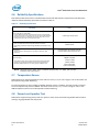
4.2
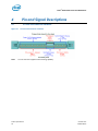
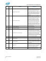
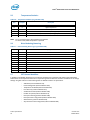
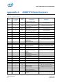
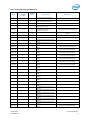
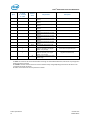
Pin Signal Definitions
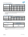
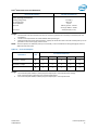
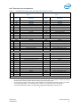
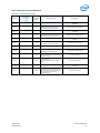
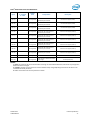
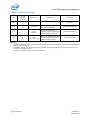
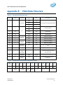
Table 16:
Pin Definition for 2.5-inch Form Factor (8639 connector specification)
Pin
Name
Description
Pin
Name
Description
S1
GND
Ground
E7
REFCLK0+
Reference clock port 0
S2
Not used (SATA/SAS)
E8
REFCLK0-
Reference clock port 0
S3
Not used (SATA/SAS)
E9
GND
Ground
Ground
E10
PETp0
Transmitter differential pair, Lane 0
S5
Not used (SATA/SAS)
E11
PETn0
Transmitter differential pair, Lane 0
S6
Not used (SATA/SAS)
E12
GND
Ground
S4
GND
S7
GND
Ground
E13
PERn0
Receiver differential pair, Lane 0
E1
REFCLK1+
Reference clock port 1 (not used)
E14
PERp0
Receiver differential pair, Lane 0
E2
REFCLK1-
Reference clock port 1 (not used)
E15
GND
Ground
E3
3.3Vaux
3.3V auxiliary power
E16
RSVD
Reserved
E4
PERST1#
Fundamental reset port 1 (not used)
S8
GND
Ground
E5
PERST0#
Fundamental reset port 0
S9
Not used (SATAe/SAS)
E6
RSVD
Reserved
S10
Not used (SATAe/SAS)
P1
Not used (SATAe/SAS)
S11
P2
Not used (SATAe/SAS)
S12
Not used (SATAe/SAS)
P3
Not used (SATAe)
S13
Not used (SATAe/SAS)
GND
Ground
P4
IfDet_N
Interface detect (drive type)
S14
GND
Ground
P5
GND
Ground
S15
RSVD
Reserved
P6
GND
Ground
S16
GND
Ground
P7
Not used (SATA/SAS)
S17
PETp1
Transmitter differential pair, Lane 1
P8
Not used (SATA/SAS)
S18
PETn1
Transmitter differential pair, Lane 1
P9
Not used (SATA/SAS)
S19
GND
Ground
P10
PRSNT_N
Presence detect (also used for
drive type)
S20
PERn1
Receiver differential pair, Lane 1
P11
Activity
Activity signal from the drive
S21
PERp1
Receiver differential pair, Lane 1
P12
Hot-Plug
Ground
S22
GND
Ground
P13
+12V_pre
12V power
S23
PETp2
Transmitter differential pair, Lane 2
P14
+12V
12V power
S24
PETn2
Transmitter differential pair, Lane 2
P15
+12V
12V power
S25
GND
Ground
S26
PERn2
Receiver differential pair, Lane 2
S27
PERp2
Receiver differential pair, Lane 2
S28
GND
Ground
E17
PETp3
Transmitter differential pair, Lane 3
E18
PETn3
Transmitter differential pair, Lane 3
October 2014
330569-004US
Product Specification
21