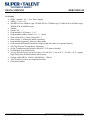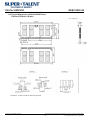
1
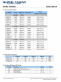
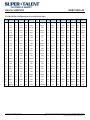
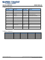
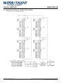
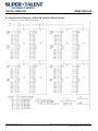
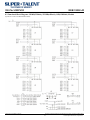
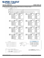
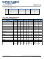
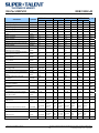
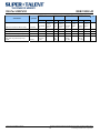
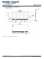
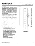
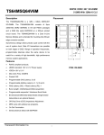
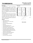
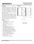
200-Pin SODIMM
DDR2 SDRAM
DDR2 SODIMM Module
256MB based on 256Mbit component
256MB, 512MB and 1GB based on 512Mbit component
1GB and 2GB based on 1Gbit component
60 Balls & 84 Balls FBGA with Pb-Free
Revision 1.0 (Mar. 2006)
-Initial Release
http://www.supertalent.com/oem
Products and Specifications discussed herein are subject to change without notice
1
© 2006 Super Talent Tech., Corporation.
200-Pin SODIMM
DDR2 SDRAM
1.0 Feature
•
•
•
•
•
•
•
•
•
•
•
•
•
•
•
•
•
•
JEDEC standard 1.8V +/- 0.1V Power Supply
VDDQ = 1.8V ± 0.1V
200 MHz fCK for 400Mb/sec/pin, 267MHz fCK for 533Mb/sec/pin, 333MHz fCK for 667Mb/sec/pin,
400MHz fCK for 800Mb/sec/pin
4 Banks
Posted CAS
Programmable CAS Latency: 3, 4, 5
Programmable Additive Latency: 0, 1 , 2 , 3 and 4
Write Latency(WL) = Read Latency(RL) –1
Burst Length: 4 , 8(Interleave/nibble sequential)
Programmable Sequential / Interleave Burst Mode
Bi-directional Differential Data-Strobe (Single-ended data-strobe is an optional feature)
Off-Chip Driver(OCD) Impedance Adjustment
On Die Termination with selectable values(50/75/150 ohms or disable)
PASR(Partial Array Self Refresh)
Average Refresh Period 7.8us at lower than a TCASE 85°C, 3.9us at 85°C < TCASE < 95 °C- support
High Temperature Self-Refresh rate enable feature
Package: 60ball FBGA - 64Mx8 , 84ball FBGA - 32Mx16
All of Lead-free products are compliant for RoHS
Gold plated contacts
http://www.supertalent.com/oem
Products and Specifications discussed herein are subject to change without notice
2
© 2006 Super Talent Tech., Corporation.
200-Pin SODIMM
DDR2 SDRAM
5.0 DIMM Pin Configurations (Front side/Back side)
Pin Front Pin Front Pin Front
Pin Front
Pin Back Pin Back
Pin Back
Pin Back
1
VREF
51
DQS2
101
A1
151
DQ42
2
VSS
52
DM2
102
A0
152
DQ46
3
Vss
53
VSS
103
VDD
153
DQ43
4
DQ4
54
VSS
104
VDD
154
DQ47
5
DQ0
55
DQ18
105
A10/AP
155
VSS
6
DQ5
56
DQ22
106
BA1
156
VSS
7
DQ1
57
DQ19
107
BA0
157
DQ48
8
VSS
58
DQ23
108
RAS#
158
DQ52
9
VSS
59
VSS
109
WE#
159
DQ49
10
DM0
60
VSS
110
S0#
160
DQ53
11
DQS0#
61
DQ24
111
VDD
161
VSS
12
VSS
62
DQ28
112
VDD
162
VSS
13
DQS0
63
DQ25
113
CAS#
163
NC
14
DQ6
64
DQ29
114
ODT0
164
CK1
15
VSS
65
VSS
115
NC/S1#
165
VSS
16
DQ7
66
VSS
116
A13
166
CK1#
17
DQ2
67
DM3
117
VDD
167
DQS6#
18
VSS
68
DQS3#
118
VDD
168
VSS
19
DQ3
69
NC
119
ODT1
169
DQS6
20
DQ12
70
DQS3
120
NC
170
DM6
21
VSS
71
VSS
121
VSS
171
VSS
22
DQ13
72
VSS
122
VSS
172
VSS
23
DQ8
73
DQ26
123
DQ32
173
DQ50
24
VSS
74
DQ30
124
DQ36
174
DQ54
25
DQ9
75
DQ27
125
DQ33
175
DQ51
26
DM1
76
DQ31
126
DQ37
176
DQ55
27
VSS
77
VSS
127
VSS
177
VSS
28
VSS
78
VSS
128
VSS
178
VSS
29
DQS1#
79
CKE0
129
DQS4#
179
DQ56
30
CK0
80
CKE1
130
DM4
180
DQ60
31
DQS1
81
VDD
131
DQS4
181
DQ57
32
CK0#
82
VDD
132
VSS
182
DQ61
33
VSS
83
NC
133
VSS
183
VSS
34
VSS
84
NC
134
DQ38
184
VSS
35
DQ10
85
BA2
135
DQ34
185
DM7
36
DQ14
86
NC
136
DQ39
186
DQS7#
37
DQ11
87
VDD
137
DQ35
187
VSS
38
DQ15
88
VDD
138
VSS
188
DQS7
39
VSS
89
A12
139
VSS
189
DQ58
40
VSS
90
A11
140
DQ44
190
VSS
41
VSS
91
A9
141
DQ40
191
DQ59
42
VSS
92
A7
142
DQ45
192
DQ62
43
DQ16
93
A8
143
DQ41
193
VSS
44
DQ20
94
A6
144
VSS
194
DQ63
45
DQ17
95
VDD
145
VSS
195
SDA
46
DQ21
96
VDD
146
DQS5#
196
VSS
47
VSS
DQS2#
97
A5
147
DM5
197
SCL
48
VSS
98
A4
148
DQS5
198
SA0
99
A3
149
VSS
199
VDDSPD
50
NC
100
A2
150
VSS
200
SA1
49
http://www.supertalent.com/oem
Products and Specifications discussed herein are subject to change without notice
4
© 2006 Super Talent Tech., Corporation.
200-Pin SODIMM
DDR2 SDRAM
6.0 Dimm Pin Description
Pin Name
Function
Pin Name
Function
A0 ~ A9, A11 ~ A13
Address input (Multiplexed)
ODT0~ODT1
On Die Termination
A10/AP
Address Input/Autoprecharge
DQ0~DQ63
Data Input/Output
Bank Select
CK0# ~ CK1#
Clock input, negative line
CK0 ~ CK1
Clock input
DM0 ~ DM7
Data Masks/Data strobes (Read)
CKE0, CKE1
Clock enable input
DQS0~DQS7
Data Strobes
S0#, S1#
Chip select input
DQS0#~DQS7#
Data strobes, negative line
RAS#
Row address strobe
VDD
Core Power
CAS#
Column address strobe
VREF
Input/Output Reference
WE#
Write Enable
VSS
Ground
SCL
SPD Clock Input
VDDSPD
SPD
SDA
SPD Data Input/Output
NC
No connection
SA0~SA1
SPD Address
BA0 ~ BA1,BA2
7.0 Address Configuration
Organization
Row Address
Column Address
Bank Address
Auto Precharge
32Mx8(256Mb) base
64Mx8(512Mb) base
32Mx16(512Mb) base
64Mx16(1Gb) base
128Mx8(1Gb) base
A0-A12
A0-A13
A0-A12
A0-A12
A0-A13
A0-A9
A0-A9
A0-A9
A0-A9
A0-A9
BA0-BA1
BA0-BA1
BA0-BA1
BA0-BA2
BA0-BA2
A10
A10
A10
A10
A10
http://www.supertalent.com/oem
Products and Specifications discussed herein are subject to change without notice
5
© 2006 Super Talent Tech., Corporation.
200-Pin SODIMM
DDR2 SDRAM
8.1 Functional Block Diagram: 256MB, 32Mx64 Module
(Populated as 1 rank of x16 SDRAM DDR2 Module)
http://www.supertalent.com/oem
Products and Specifications discussed herein are subject to change without notice
6
© 2006 Super Talent Tech., Corporation.
200-Pin SODIMM
DDR2 SDRAM
8.2 Functional Block Diagram: 512MB/1GB, 64Mx64/128Mx64 Module
(Populated as 2 ranks of x16 SDRAM DDR2 Module)
http://www.supertalent.com/oem
Products and Specifications discussed herein are subject to change without notice
7
© 2006 Super Talent Tech., Corporation.
200-Pin SODIMM
DDR2 SDRAM
8.3 Functional Block Diagram: 256MB(32Mx64), 512MB(64Mx64), 1GB(128Mx64) Module
(Populated as 2 ranks of x8 SDRAM DDR2 Module)
http://www.supertalent.com/oem
Products and Specifications discussed herein are subject to change without notice
8
© 2006 Super Talent Tech., Corporation.
200-Pin SODIMM
DDR2 SDRAM
8.4 Functional Block Diagram: 1GB and 2GB, 128Mx64 and 256Mx64 Module
(Populated as 2 ranks of x8 SDRAM DDR2 Module)
http://www.supertalent.com/oem
Products and Specifications discussed herein are subject to change without notice
9
© 2006 Super Talent Tech., Corporation.
200-Pin SODIMM
DDR2 SDRAM
9.0 AC & DC Operating Conditions
Recommended operating conditions (Voltage referenced to Vss=0V, TA=0 to 70°C)
Symbol
Parameter
Min
Typ
Max
Unit
VDD
VDDL
VDDQ
VREF
VTT
Supply Voltage
Supply Voltage for DLL
Supply Voltage for Output
Input Reference Voltage
Termination Voltage
1.7
1.7
1.7
0.49*VDDQ
VREF-0.04
1.8
1.8
1.8
0.50*VDDQ
VREF
1.9
1.9
1.9
0.51*VDDQ
VREF+0.04
V
V
V
mV
V
10.0 AC Timing Parameters & Specifications
(AC operating conditions unless otherwise noted)
Parameter
Symbol
DDR2-800
DDR2-667
DDR2-533
DDR2-400
max
+400
min
-450
max
+450
min
-500
max
+500
min
-600
max
+600
ps
Units
DQ output access time from CK/CK
tAC
min
- 400
DQS output access time from CK/CK
tDQSCK
-350
+350
-400
+400
-450
+450
-500
+500
ps
CK high-level width
tCH
0.45
0.55
0.45
0.55
0.45
0.55
0.45
0.55
tCK
CK low-level width
tCL
0.55
tCK
tCK
0.45
min(tC
L, tCH
5000
0.55
Clock cycle time, CL=x
0.45
min(tC
L, tCH
3750
0.55
tHP
0.45
min(tC
L, tCH
3000
0.55
CK half period
0.45
min(tCL
,tCH)
2500
DQ and DM input hold time
tDH(base)
125
x
175
x
225
x
DQ and DM input setup time
Control & Address input pulse width
for each input
DQ and DM input pulse width for each
input
Data-out high-impedance time from
CK/CK
DQS low-impedance time from CK/CK
tDS(base)
50
x
100
x
100
tIPW
0.6
x
0.6
x
tDIPW
0.35
x
0.35
x
tLZ(DQS)
tAC min
DQ low-impedance time from CK/CK
tLZ(DQ)
2*tAC
min
tHZ
DQS-DQ skew for DQS and associated
DQ signals
DQ hold skew factor
tQHS
DQ/DQS output hold time from DQS
tQH
First DQS latching transition to
associated clock edge
tDQSS
http://www.supertalent.com/oem
tDQSQ
x
x
8000
tAC
max
tAC
max
tAC
max
x
200
x
tHP tQHS
300
-0.25
0.25
x
tAC
min
2*tAC
min
x
x
x
8000
tAC
max
tAC
max
tAC
max
240
x
tHP tQHS
340
-0.25
0.25
x
x
ps
8000
ps
275
x
ps
x
150
x
ps
0.6
x
0.6
x
tCK
0.35
x
0.35
x
tCK
x
tAC
min
2*tAC
min
x
x
8000
tAC
max
tAC
max
tAC
max
tAC
min
2*tAC
min
tAC
max
tAC
max
tAC
max
300
x
350
ps
x
tHP tQHS
450
ps
-0.25
0.25
x
tHP tQHS
400
-0.25
0.25
x
x
x
ps
ps
ps
ps
tCK
Products and Specifications discussed herein are subject to change without notice
10
© 2006 Super Talent Tech., Corporation.
200-Pin SODIMM
Parameter
DQS input high pulse width
DQS input low pulse width
DQS falling edge to CK setup time
DQS falling edge hold time from CK
Mode register set command cycle
timet
Write postamble
Write preamble
Address and control input hold time
Address and control input setup time
Read preamble
Read postamble
Active to active command period for
1KB page size products
Active to active command period for
2KB page size products
Four Activate Window for 1KB page
size productst
Four Activate Window for 2KB page
size products
CAS to CAS command delay
DDR2 SDRAM
DDR2-800
DDR2-667
DDR2-533
DDR2-400
Units
tDQSH
tDQSL
tDSS
tDSH
min
0.35
0.35
0.2
0.2
max
x
x
x
x
min
0.35
0.35
0.2
0.2
min
0.35
0.35
0.2
0.2
min
0.35
0.35
0.2
0.2
tCK
tCK
tCK
tCK
tMRD
2
x
2
x
2
x
2
x
tCK
tWPST
tWPRE
tIH(base)
tIS(base)
tRPRE
tRPST
0.4
0.35
250
175
0.9
0.4
0.6
x
x
x
1.1
0.6
0.4
0.35
275
200
0.9
0.4
0.6
x
x
x
1.1
0.6
0.4
0.35
375
250
0.9
0.4
0.6
x
x
x
1.1
0.6
0.4
0.35
475
350
0.9
0.4
0.6
x
x
x
1.1
0.6
tCK
tCK
ps
ps
tCK
tCK
tRRD
7.5
x
7.5
x
7.5
x
7.5
x
ns
tRRD
10
x
10
x
10
x
10
x
ns
tFAW
35
tFAW
tCCD
tWR
45
2
15
x
x
tDAL
WR+tRP
x
tWTR
tRTP
Symbol
max
x
x
x
x
max
x
x
x
x
max
x
x
x
x
37.5
37.5
37.5
ns
50
2
15
WR+
tRP
x
x
x
x
50
2
15
WR+t
RP
ns
tCK
ns
x
50
2
15
WR+tR
P
x
tCK
7.5
7.5
x
7.5
x
10
x
ns
tXSNRt
7.5
tRFC +
10
7.5
tRFC
+ 10
Exit self refresh to a read command
Exit precharge power down to any
non-read command
Exit active power down to read
command
Exit active power down to read
command(slow exit, lower power)
CKE minimum pulse width(high and
low pulse width)
tXSRD
tXP
200
2
x
200
2
x
200
2
x
200
2
x
tXARD
2
x
2
x
2
x
2
x
ODT turn-on delay
ODT turn-on
Write recovery time
Auto precharge write recovery +
precharge time
Internal write to read command delay
Internal read to precharge command
delay
Exit self refresh to a non-read
command
7.5
tRFC
+ 10
ns
ns
tCK
tCK
tCK
tXARDS
8 - AL
tCKE
3
tAOND
2
tAON
tAC(min)
ODT turn-on(Power-Down mode)
ODT turn-off delay
tAONPD
tAOFD
ODT turn-off
tAOF
http://www.supertalent.com/oem
7.5
tRFC +
10
7AL
6 - AL
3
3
2
tAC(max
) + 0.7
2
tAC(
min)
2
tAC(ma
x)+0.7
2
tAC(mi
n)
tAC(
min)
+2
2.5
2tCK
+tAC(m
ax)+1
2.5
tAC(mi
n)+2
2.5
2tCK
+tAC(m
ax)+1
2.5
2.5
tAC(min)
tAC(max
)+ 0.6
tAC(
min)
tAC(ma
x)+ 0.6
tAC(mi
n)
tAC(min)
+2
6 - AL
tCK
3
2
tAC(m
ax)+1t
2tCK
+tAC(
max)+
1
2
tAC(m
in)
2.5
tAC(m
ax)+
0.6
2.5
tAC(m
in)+2
tAC(m
in)
tCK
2
tAC(m
ax)+1t
2tCK
+tAC(
max)+
1
2.5
tAC(m
ax)+
0.6
tCK
ns
ns
tCK
ns
Products and Specifications discussed herein are subject to change without notice
11
© 2006 Super Talent Tech., Corporation.
200-Pin SODIMM
Parameter
DDR2 SDRAM
DDR2-800
DDR2-667
DDR2-533
DDR2-400
min
max
min
max
min
min
2.5tCK
+tAC(m
ax)+1
tAC(
min)
+2
3
2.5tCK
+tAC(m
ax)+1
ODT turn-off (Power-Down mode)
ODT to power down entry latency
tAOFPD
tANPD
tAC(min)
+2
3
ODT power down exit latency
OCD drive mode output delay
Minimum time clocks remains ON
after CKE asynchronously drops
LOW
tAXPD
tOIT
8
0
tDelay
tIS+tCK
+tIH
http://www.supertalent.com/oem
Units
Symbol
8
0
tIS+t
CK
+tIH
12
12
tAC(mi
n)+2
3
8
0
tIS+tC
K +tIH
max
2.5tCK
+tAC(
max)+
1
12
tAC(m
in)+2
3
8
0
tIS+tC
K +tIH
max
2.5tCK
+tAC(
max)+
1
12
ns
tCK
tCK
ns
ns
Products and Specifications discussed herein are subject to change without notice
12
© 2006 Super Talent Tech., Corporation.
200-Pin SODIMM
DDR2 SDRAM
11.1 Physical Dimensions: (32Mx16Based)
32Mx64 (1 Rank)
Units : Millimeters
Tolerances :± 0.005(.13) unless otherwise specified
http://www.supertalent.com/oem
Products and Specifications discussed herein are subject to change without notice
13
© 2006 Super Talent Tech., Corporation.
200-Pin SODIMM
DDR2 SDRAM
11.2 Physical Dimensions: (32Mx8/64Mx8/128Mx8 Based) and (32Mx16/64Mx16 Based)
32Mx64/64Mx64/128Mx64 (1 Rank) and 64Mx64/128Mx64 (2 Ranks)
Units : Millimeters
Tolerances :± 0.005(.13) unless otherwise specified
http://www.supertalent.com/oem
Products and Specifications discussed herein are subject to change without notice
14
© 2006 Super Talent Tech., Corporation.
200-Pin SODIMM
DDR2 SDRAM
11.3 Physical Dimensions: (64Mx8/128Mx8 Based)
128Mx64/256Mx64 (2 Ranks)
Units : Millimeters
Tolerances :± 0.005(.13) unless otherwise specified
http://www.supertalent.com/oem
Products and Specifications discussed herein are subject to change without notice
15
© 2006 Super Talent Tech., Corporation.