1
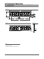
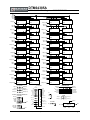
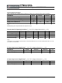
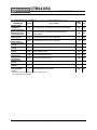
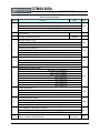
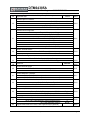
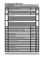
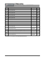
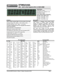
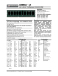
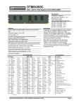
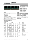
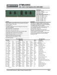
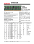
DTM64385A 16GB - 240-Pin 2Rx4 Registered ECC DDR3 DIMM Identification DTM64385A 1Gx72 16GB 2Rx4 PC3-12800R-11-11-E2 Performance range Clock / Module Speed / CL-tRCD -tRP 800 MHz / PC3-12800 / 11-11-11 667 MHz / PC3-10600 / 10-10-10 667 MHz / PC3-10600 / 9-9-9 533 MHz / PC3-8500 / 8-8-8 533 MHz / PC3-8500 / 7-7-7 400 MHz / PC3-6400 / 6-6-6 Features Description 240-pin JEDEC-compliant DIMM, 133.35 mm wide by 30 mm high DTM64385A is a registered 2Gx72 memory module, which conforms to JEDEC's DDR3, PC3-12800 standard. The assembly is Dual-Rank. Each Rank is comprised of eighteen Samsung 1Gx4 DDR3-1600 SDRAMs. One 2Kbit EEPROM is used for Serial Presence Detect and a combination register/PLL, with Address and Command Parity, is also used. Operating Voltage: 1.5V ±0.075 I/O Type: SSTL_15 On-board I2C temperature sensor with integrated Serial PresenceDetect (SPD) EEPROM Data Transfer Rate: 12.8 Gigabytes/sec Both output driver strength and input termination impedance are programmable to maintain signal integrity on the I/O signals in a Fly-by topology. A thermal sensor accurately monitors the DIMM module and can prevent exceeding the maximum operating temperature of 95C. Data Bursts: 8 and burst chop 4 mode ZQ Calibration for Output Driver and On-Die Termination (ODT) Programmable ODT / Dynamic ODT during Writes Programmable CAS Latency: 6, 7, 8, 9, 10, and 11 Bi-directional Differential Data Strobe signals SDRAM Addressing (Row/Col/Bank): 16/11/3 Fully RoHS Compliant Pin Configuration Front Side Pin Description Back Side Name Function 1 VREFDQ 31 DQ25 61 A2 91 DQ41 121 VSS 151 VSS 181 A1 211 VSS CB[7:0] Data Check Bits 2 VSS 32 VSS 62 VDD 92 VSS 122 DQ4 152 DQS12 182 VDD 212 DQS14 DQ[63:0] Data Bits 3 4 5 6 33 34 35 36 63 CK1* 64 /CK1* 65 VDD 66 VDD 93 94 95 96 /DQS5 DQS5 VSS DQ42 123 124 125 126 153 154 155 156 183 184 185 186 213 214 215 216 DQS[17:0], /DQS[17:0] CK[1:0], /CK[1:0] CKE[1:0] /CAS Differential Data Strobes Differential Clock Inputs Clock Enables Column Address Strobe 7 DQS0 37 DQ27 8 VSS 38 VSS 9 DQ2 39 CB0 67 VREFCA 68 PAR_IN 69 VDD 97 98 99 DQ43 VSS DQ48 127 VSS 128 DQ6 129 DQ7 157 VSS 158 CB4 159 CB5 187 /EVENT 188 A0 189 VDD 217 VSS 218 DQ52 219 DQ53 /RAS /S[3:0] /WE Row Address Strobe Chip Selects Write Enable 10 DQ3 11 VSS 12 DQ8 40 CB1 41 VSS 42 /DQS8 70 A10/AP 71 BA0 72 VDD 100 DQ49 101 VSS 102 /DQS6 130 VSS 131 DQ12 132 DQ13 160 VSS 161 DQS17 162 /DQS17 190 BA1 191 VDD 192 /RAS 220 VSS 221 DQS15 222 /DQS15 A[15:0] BA[2:0] ODT[1:0] Address Inputs Bank Addresses On Die Termination Inputs 13 DQ9 43 DQS8 73 /WE 103 DQS6 133 VSS 163 VSS 193 /S0 223 VSS SA[2:0] SPD Address 14 15 16 17 44 45 46 47 74 75 76 77 104 105 106 107 134 135 136 137 164 165 166 167 194 195 196 197 224 225 226 227 SCL SDA /EVENT /RESET SPD Clock Input SPD Data Input/Output Temperature Sensing Reset for register and DRAMs DQ0 DQ1 VSS /DQS0 VSS /DQS1 DQS1 VSS /DQS3 DQS3 VSS DQ26 VSS CB2 CB3 VSS /CAS VDD /S1 ODT1 18 DQ10 19 DQ11 20 VSS 48 VTT 49 VTT 50 CKE0 21 DQ16 51 VDD 81 DQ32 22 DQ17 52 BA2 82 DQ33 23 24 25 26 27 53 54 55 56 57 83 84 85 86 87 113 114 115 116 117 VSS /DQS2 DQS2 VSS DQ18 28 DQ19 29 VSS 30 DQ24 /ERR_OUT VDD A11 A7 VDD 58 A5 59 A4 60 VDD VSS DQ50 DQ51 VSS 78 VDD 108 DQ56 79 /S2, NC 109 DQ57 80 VSS 110 VSS VSS /DQS4 DQS4 VSS DQ34 88 DQ35 89 VSS 90 DQ40 DQ5 VSS DQS9 /DQS9 DQS10 /DQS10 VSS DQ14 /DQS12 VSS DQ30 DQ31 CB6 CB7 VSS NC (TEST) VDD CK0 /CK0 VDD VDD ODT0 A13 VDD /DQS14 VSS DQ46 DQ47 DQ54 DQ55 VSS DQ60 138 DQ15 139 VSS 140 DQ20 168 /RESET 169 CKE1 170 VDD 198 /S3, NC 199 VSS 200 DQ36 228 DQ61 229 VSS 230 DQS16 PAR_IN /ERR_OUT A12/BC Parity bit for Addr/Ctrl Error bit for Parity Error Combination input: Addr12/Burst Chop 111 /DQS7 141 DQ21 171 A15 201 DQ37 231 /DQS16 A10/AP Combination input: Addr10/Auto-precharge 112 DQS7 142 VSS 172 A14 202 VSS 232 VSS VSS Ground 143 144 145 146 147 173 174 175 176 177 203 204 205 206 207 233 234 235 236 237 VDD VDDSPD VREFDQ VREFCA VTT Power SPD EEPROM Power Reference Voltage for DQ’s Reference Voltage for CA Termination Voltage NC No Connection * not used VSS DQ58 DQ59 VSS SA0 118 SCL 119 SA2 120 VTT DQS11 /DQS11 VSS DQ22 DQ23 148 VSS 149 DQ28 150 DQ29 VDD A12/BC A9 VDD A8 178 A6 179 VDD 180 A3 DQS13 /DQS13 VSS DQ38 DQ39 208 VSS 209 DQ44 210 DQ45 Document 06976, Revision A, 10-Nov-11, Dataram Corporation 2011 DQ62 DQ63 VSS VDDSPD SA1 238 SDA 239 VSS 240 VTT Page 1 DTM64385A 16GB - 240-Pin 2Rx4 Registered ECC DDR3 DIMM Front view 133.35 [5.250] 9.50 [0.374] 30.00 [1.181] 17.30 [0.681] 5.00 [0.197] 5.175 [0.204] 47.00 [1.850] 71.00 [2.795] 2.50 [0.098] 123.00 [4.843] Back view Side view 3.94 Max [0.155] Max 4.00 Min [0.157] Min 1.27 ±.10 [0.0500 ±0.0040] Notes Tolerances on all dimensions except where otherwise indicated are ±.13 (.005). All dimensions are expressed: millimeters [inches] Document 06976, Revision A, 10-Nov-11, Dataram Corporation 2011 Page 2 DTM64385A 16GB - 240-Pin 2Rx4 Registered ECC DDR3 DIMM /RS1 /RS0 /DQS0 DQS0 V SS /DQS9 DQS9 /DQS CS DQS DQR[3:0] /CS DM /DOS DOS CS I/O[3:0] CS DM /DQS DQS CS I/O[3:0] /DOS DOS CS CS DM I/O[3:0] /DQS10 DQS10 /DQS1 DQS1 /DQS DQR[11:8] DQS CS /CS DM /DOS DOS CS I/O[3:0] CS DM I/O[3:0] /DQS DQS CS DQR[15:12] /DOS DOS CS /CS DM I/O[3:0] I/O[7:0] CS DM I/O[3:0] /DQS11 DQS11 /DQS2 DQS2 /DQS DQS CS DQR[19:16] /CS DM I/O[3:0] DQR[7:4] /DQS /DOS DQS DOS CS /CS DM I/O[7:0] I/O[3:0] /CS CS DM DM I/O[3:0] /DQS DQS CS DQR[23:20] /DQS DQS CS /DOS DOS CS /CS DM I/O[3:0] I/O[7:0] CS DM I/O[3:0] /DQS DQS CS DQR[31:28] /DOS DOS CS /CS DM I/O[3:0] I/O[7:0] CS DM I/O[3:0] /DQS17 DQS17 /DQS8 DQS8 /DQS DQS CS CBR[3:0] /DOS DOS CS /CS DM /DQS DQS CS CS DM CBR[7:4] I/O[3:0] I/O[3:0] I/O[7:0] /DQS4 DQS4 /DOS DOS CS /CS DM CS DM I/O[3:0] I/O[3:0] I/O[7:0] /DQS13 DQS13 /DQS DQS CS DQR[35:32] /DQS DQS /DOS DOS CS /CS DM I/O[3:0] I/O[7:0] /CS CS DM DM I/O[3:0] /DQS DQS CS /DOS DOS CS /CS DM CS DM I/O[3:0] I/O[3:0] I/O[7:0] DQR[39:36] /DQS14 DQS14 /DQS5 DQS5 /DQS DQS CS DQR[43:40] CS DM I/O[3:0] /DQS12 DQS12 /DQS3 DQS3 DQR[27:24] /DOS DOS CS /CS DM I/O[3:0] I/O[7:0] /DOS DOS CS /CS DM I/O[3:0] I/O[7:0] CS DM /DQS DQS CS DQR[47:44] I/O[3:0] /DOS DOS CS /CS DM I/O[3:0] I/O[7:0] CS DM I/O[3:0] /DQS15 DQS15 /DQS6 DQS6 /DQS DQS CS DQR[51:48] /DOS DOS CS /CS DM I/O[3:0] I/O[7:0] /DQS DQS CS CS DM I/O[3:0] /DQS7 DQS7 /DOS DOS CS /CS DM I/O[3:0] I/O[7:0] DQR[55:52] CS DM I/O[3:0] /DQS16 DQS16 /DOS DOS CS /CS DM I/O[3:0] I/O[7:0] CBR[7:0] DQS[17:0] DQSR[17:0] /DQS[17:0] /DQSR[17:0] GLOBAL SDRAM CONNECTS A[15:0] /RAS /CAS /WE CKE[1:0] All 36 OHMS BA[2:0]R ODT[1:0] A[15:0]R /RASR PAR_IN /CASR /WER VTT All 36 OHMS CKE[1:0]R ODT[1:0]R /RS[1:0] CK0 120 OHMS /CK0 CKE[1:0]R ODT[1:0]R CK1 All SDRAMs 36 OHMS /CK1 /LCLK[1:0] LCLK[1:0] /RCLK[1:0] RCLK[1:0] /ERR_OUT /EVENT L,R(CLK)[1:0] /L,R(CLK)[1:0] Serial PD All Devices All SDRAMs All Devices All SDRAMs 120 OHMS All 240 OHMS ZQ /RESET VTT DECOUPLING VDDSPD VDD VREF_DQ VSS VREF_CA VTT /RS0 /RS1 BA[2:0]R A[15:0]R /RASR /CASR /WER CS DM I/O[3:0] All 22 OHMS /S0 /S1 BA[2:0] /DOS DOS CS /CS DM I/O[3:0] I/O[7:0] TO SDRAMS DQR[63:0] CB[7:0] /DQS DQS CS DQR[63:60] All 15 OHMS DQ[63:0] CS DM I/O[3:0] REG / PLL /DQS DQS CS DQR[59:56] SCL V SS SDRAMS Document 06976, Revision A, 10-Nov-11, Dataram Corporation 2011 TEMPERATURE MONITOR/ SERIAL PD SA0 SA1 SDA SA2 Page 3 DTM64385A 16GB - 240-Pin 2Rx4 Registered ECC DDR3 DIMM Absolute Maximum Ratings (Note: Operation at or above Absolute Maximum Ratings can adversely affect module reliability.) PARAMETER Symbol Minimum Maximum Unit Temperature, non-Operating TSTORAGE -55 100 C TA 0 70 C Ambient Temperature, Operating DRAM Case Temperature, Operating TCASE 0 95 C VDD -0.4 1.975 V VIN,VOUT -0.4 1.975 V Voltage on VDD relative to VSS Voltage on Any Pin relative to VSS Notes: DRAM Operating Case Temperature above 85C requires 2X refresh. Recommended DC Operating Conditions (TA = 0 to 70 C, Voltage referenced to Vss = 0 V) PARAMETER Power Supply Voltage Symbol VDD Minimum 1.425 Typical 1.5 Maximum 1.575 Unit V Note SPD EEPROM Voltage VDDSPD 3.0 3.3 3.6 V I/O Reference Voltage VREFDQ 0.49 VDD 0.50 VDD 0.51 VDD V 1 I/O Reference Voltage VREFCA 0.49 VDD 0.50 VDD 0.51 VDD V 1 Notes: 1) The value of VREF is expected to equal one-half VDD and to track variations in the VDD DC level. Peak-to-peak noise on VREF may not exceed ±1% of its DC value. DC Input Logic Levels, Single-Ended (TA = 0 to 70 C, Voltage referenced to Vss = 0 V) PARAMETER Logical High (Logic 1) Symbol VIH(DC) Minimum VREF + 0.1 Maximum VDD Unit V Logical Low (Logic 0) VIL(DC) VSS VREF - 0.1 V AC Input Logic Levels, Single-Ended (TA = 0 to 70 C, Voltage referenced to Vss = 0 V) PARAMETER Logical High (Logic 1) Symbol VIH(AC) Minimum VREF + 0.175 Maximum - Unit V Logical Low (Logic 0) VIL(AC) - VREF - 0.175 V Document 06976, Revision A, 10-Nov-11, Dataram Corporation 2011 Page 4 DTM64385A 16GB - 240-Pin 2Rx4 Registered ECC DDR3 DIMM Differential Input Logic Levels (TA = 0 to 70 C, Voltage referenced to Vss = 0 V) PARAMETER Differential Input Logic High Differential Input Logic Low Differential Input Cross Point Voltage relative to VDD/2 Symbol VIH.DIFF Minimum +0.200 Maximum DC:VDD AC:VDD+0.4 Unit V VIL.DIFF DC:VSS AC:VSS-0.4 -0.200 V VIX - 0.150 + 0.150 V Capacitance (TA = 25 C, f = 100 MHz) PARAMETER Pin Symb ol Minimu m Maximum Unit Input Capacitance, Clock CK0, /CK0 CCK 1.5 2.5 pF Input Capacitance, Address BA[2:0], A[15:0], /RAS, /CAS, /WE CI 1.5 2.5 pF Input Capacitance Control /S[1:0], CKE[1:0], ODT[1:0] CI 1.5 2.5 pF Input/Output Capacitance DQ[63:0], CB[7:0], DQS[17:0], /DQS[17:0]. CIO 3 5 pF DC Characteristics (TA = 0 to 70 C, Voltage referenced to Vss = 0 V) PARAMETER Input Leakage Current Symbol Minimum Maximum Unit Note IIL -18 +18 µA 1,2 IOL -10 +10 µA 2,3 (Any input 0 V < VIN < VDD) Output Leakage Current (0V < VOUT < VDDQ) Notes: 1) All other pins not under test = 0 V 2) Values are shown per pin 3) DQ, DQS, DQS and ODT are disabled Document 06976, Revision A, 10-Nov-11, Dataram Corporation 2011 Page 5 DTM64385A 16GB - 240-Pin 2Rx4 Registered ECC DDR3 DIMM IDD Specifications and Conditions (TA = 0 to 70 C, Voltage referenced to Vss = 0 V) PARAMETER Operating One Bank ActivePrecharge Current Operating One Bank Active-ReadPrecharge Current Precharge PowerDown Current Precharge PowerDown Current Precharge Standby Current Active Power-Down Current Active Standby Current Operating Burst Write Current Operating Burst Read Current Burst Refresh Current Self Refresh Current Operating Bank Interleave Read Current Symbol Test Condition Max Value Unit IDD0* Operating current : One bank ACTIVATE-to-PRECHARGE 1900 mA IDD1* Operating current : One bank ACTIVATE-to-READ-toPRECHARGE 2080 mA IDD2P** Precharge power down current: (Slow exit) 770 mA IDD2P** Precharge power down current: (Fast exit) 770 mA IDD2N** Precharge standby current 1430 mA IDD3P** Active power-down current 950 mA IDD3N** Active standby current 1820 mA IDD4W* Burst write operating current 2800 mA IDD4R* Burst read operating current 2670 mA IDD5B** Refresh current 3680 mA IDD6** Self-refresh temperature current: MAX TC = 85°C 550 mA IDD7* All bank interleaved read current 4080 mA * One module rank in this operation, the rest in IDD2P slow exit. ** All module ranks in this operation. Document 06976, Revision A, 10-Nov-11, Dataram Corporation 2011 Page 6 DTM64385A 16GB - 240-Pin 2Rx4 Registered ECC DDR3 DIMM AC Operating Conditions PARAMETER Symbol Min Max Unit Internal read command to first data tAA 13.125 20 ns CAS-to-CAS Command Delay tCCD 4 - tCK tCH(avg) 0.47 0.53 tCK tCK 1.25 2.500 ns tCL(avg) 0.47 0.53 tCK tDH 45 - ps Clock High Level Width Clock Cycle Time Clock Low Level Width Data Input Hold Time after DQS Strobe DQ Input Pulse Width tDIPW 360 - ps DQS Output Access Time from Clock tDQSCK -225 +225 ps Write DQS High Level Width tDQSH 0.45 0.55 tCK(avg) Write DQS Low Level Width tDQSL 0.45 0.55 tCK(avg) DQS-Out Edge to Data-Out Edge Skew tDQSQ - 100 ps Data Input Setup Time Before DQS Strobe tDS 10 - ps DQS Falling Edge from Clock, Hold Time tDSH 0.2 - tCK(avg) DQS Falling Edge to Clock, Setup Time tDSS 0.2 - tCK(avg) Clock Half Period tHP minimum of tCH or tCL - ns Address and Command Hold Time after Clock tIH 120 - ps Address and Command Setup Time before Clock tIS 45 - ps Load Mode Command Cycle Time tMRD 4 - tCK DQ-to-DQS Hold tQH 0.38 - tCK(avg) Active-to-Precharge Time tRAS 35 9*tREFI ns Active-to-Active / Auto Refresh Time tRC 48.125 - ns RAS-to-CAS Delay tRCD 13.125 - ns - 7.8 µs o o tREFI o o Average Periodic Refresh Interval 0 C < TCASE < 95 C tREFI - 3.9 µs Auto Refresh Row Cycle Time tRFC 260 - ns Row Precharge Time tRP 13.125 - ns Read DQS Preamble Time tRPRE 0.9 Note-1 tCK(avg) Read DQS Postamble Time tRPST 0.3 Note-2 tCK(avg) Row Active to Row Active Delay tRRD Max(4nCK, 6ns) - ns Internal Read to Precharge Command Delay tRTP Max(4nCK, 7.5ns) - ns Write DQS Preamble Setup Time tWPRE 0.9 - tCK(avg) Write DQS Postamble Time tWPST 0.3 - tCK(avg) Write Recovery Time tWR 15 - ns Internal Write to Read Command Delay tWTR Max(4nCK, 7.5ns) - ns Average Periodic Refresh Interval 0 C < TCASE < 85 C Notes: 1. 2. The maximum preamble is bound by tLZDQS(min) The maximum postamble is bound by tHZDQS(max) Document 06976, Revision A, 10-Nov-11, Dataram Corporation 2011 Page 7 DTM64385A 16GB - 240-Pin 2Rx4 Registered ECC DDR3 DIMM Serial Presence Detect Byte# Function. Value Hex 176 256 Bytes 0-116 0x92 SPD Revision. Rev. 1.1 0x11 Key Byte / DRAM Device Type. DDR3 SDRAM 0x0B Number of Bytes Used / Number of Bytes in SPD Device / CRC Coverage. Bit 3 ~ Bit 0. SPD Bytes Used Bit 6 ~ Bit 4. SPD Bytes Total Bit 7. CRC Coverage - 0 1 2 Key Byte / Module Type. 3 4 Bit 3 ~ Bit 0. Module Type Bit 7 ~ Bit 4. Reserved - RDIMM 0 0x01 SDRAM Density and Banks. Bit 3 ~ Bit 0. Total SDRAM capacity, in megabits Bit 6 ~ Bit 4. Bank Address Bits Bit 7. Reserved - 4Gb 8 banks 0 0x04 11 16 0 0x22 SDRAM Addressing. Bit 2 ~ Bit 0. Column Address Bits Bit 5 ~ Bit 3. Row Address Bits Bit 7, 6. Reserved 5 Module Nominal Voltage, VDD. Bit 0. NOT 1.5 V operable Bit 1. 1.35 V operable Bit 2. 1.2X V operable Bit 3. Reserved Bit 4. Reserved Bit 5. Reserved Bit 6. Reserved Bit 7. Reserved - 6 0x00 Module Organization. 7 Bit 2 ~ Bit 0. SDRAM Device Width Bit 5 ~ Bit 3. Number of Ranks Bit 7, 6. Reserved 4-Bits 2-Rank 0 0x08 Bit 2 ~ Bit 0. Primary bus width, in bits Bit 4, Bit 3. Bus width extension, in bits Bit 7 ~ Bit 5. Reserved - 64-Bits 8-Bits 0 0x0B 1 1 1 (MTB = 0.125ns) 0x11 Module Memory Bus Width. 8 9 10 Fine Timebase (FTB) Dividend / Divisor. Bit 3 ~ Bit 0. Fine Timebase (FTB) Divisor Bit 7 ~ Bit 4. Fine Timebase (FTB) Dividend Medium Timebase (MTB) Dividend. Document 06976, Revision A, 10-Nov-11, Dataram Corporation 2011 0x01 Page 8 DTM64385A 16GB - 240-Pin 2Rx4 Registered ECC DDR3 DIMM 11 Medium Timebase (MTB) Divisor. 12 SDRAM Minimum Cycle Time (tCKmin). 13 Reserved. 8 (MTB = 0.125ns) 0x08 1.25ns 0x0A UNUSED 0x00 CAS Latencies Supported, Least Significant Byte. Bit 0. CL = 4 Bit 1. CL = 5 Bit 2. CL = 6 Bit 3. CL = 7 Bit 4. CL = 8 Bit 5. CL = 9 Bit 6. CL = 10 Bit 7. CL = 11 - 14 X X X X X X 0xFC CAS Latencies Supported, Most Significant Byte. Bit 0. CL = 12 Bit 1. CL = 13 Bit 2. CL =14 Bit 3. CL = 15 Bit 4. CL = 16 Bit 5. CL = 17 Bit 6. CL = 18 Bit 7. Reserved. 15 16 Minimum CAS Latency Time (tAAmin). 17 Minimum Write Recovery Time (tWRmin). 18 Minimum RAS# to CAS# Delay Time (tRCDmin). 19 Minimum Row Active to Row Active Delay Time (tRRDmin). 20 Minimum Row Precharge Delay Time (tRPmin). 21 22 23 24 25 26 27 28 Upper Nibbles for tRAS and tRC. Bit 3 ~ Bit 0. tRAS Most Significant Nibble Bit 7 ~ Bit 4. tRC Most Significant Nibble Minimum Active to Precharge Delay Time (tRASmin), Least Significant Byte. Minimum Active to Active/Refresh Delay Time (tRCmin), Least Significant Byte. Minimum Refresh Recovery Delay Time (tRFCmin), Least Significant Byte. Minimum Refresh Recovery Delay Time (tRFCmin), Most Significant Byte. Minimum Internal Write to Read Command Delay Time (tWTRmin). Minimum Internal Read to Precharge Command Delay Time (tRTPmin). Upper Nibble for tFAW. Bit 3 ~ Bit 0. tFAW Most Significant Nibble Bit 7 ~ Bit 4. Reserved - Document 06976, Revision A, 10-Nov-11, Dataram Corporation 2011 0x00 13.125ns 0x69 15.0ns 0x78 13.125ns 0x69 6.0ns 0x30 13.125ns 0x69 1 1 0x11 35.0ns 0x18 48.125ns 0x81 260.0ns 0x20 260.0ns 0x08 7.5ns 0x3C 7.5ns 0x3C 0 0 0x00 Page 9 DTM64385A 16GB - 240-Pin 2Rx4 Registered ECC DDR3 DIMM 29 Minimum Four Activate Window Delay Time (tFAWmin), Least Significant Byte. 30.0ns 0xF0 Bit 0. RZQ / 6 Bit 1. RZQ / 7 Bit 6 ~ Bit 2. Reserved Bit 7. DLL-Off Mode Support X X 0x83 Extended Temperature Range Extended Temperature Refresh Rate Auto Self Refresh (ASR) On-die Thermal Sensor (ODTS) Readout Reserved Reserved Reserved Partial Array Self Refresh (PASR) - X SDRAM Optional Features. 30 SDRAM Drivers Supported. 31 0x01 Module Thermal Sensor. 32 Bit 6 ~ Bit 0. Thermal Sensor Accuracy Bit 7. Thermal Sensor - 0 With TS Bit 6 ~ Bit 0. Non-Standard Device Description Bit 7. SDRAM Device Type - 0 Std Mono 0x80 SDRAM Device Type. 33 34 -59 Reserved UNUSED 0x00 0x00 Module Nominal Height. 60 Bit 4 ~ Bit 0. Module Nominal Height max, in mm Bit 7 ~ Bit5. Reserved - 29<h<=30 0 0x0F 1<th<=2 1<th<=2 0x11 R/C E Rev.2 0 0x44 1 Register 2 Rows 0 0x09 0 No HS 0x00 Module Maximum Thickness. 61 Bit 3 ~ Bit 0. Front, in mm (baseline thickness = 1 mm) Bit 7 ~ Bit 4. Back, in mm (baseline thickness = 1 mm) Reference Raw Card Used. 62 Bit 4 ~ Bit 0. Reference Raw Card Bit 6, Bit 5. Reference Raw Card Revision Bit 7. Reserved (Registered) DIMM Module Attributes. 63 Bit 1 ~ Bit 0. # of Registers used on RDIMM Bit 3 ~ Bit 2. # of Rows of DRAMs on RDIMM Bit 7 ~ Bit 4. Reserved RDIMM Thermal Heat Spreader Solution. 64 65 Bit 6 ~ Bit 0. Heat Spreader Thermal Characteristics Bit 7. Heat Spreader Solution Register Manufacturer ID Code, Least Significant Byte (Optional). Document 06976, Revision A, 10-Nov-11, Dataram Corporation 2011 0x80 Page 10 DTM64385A 16GB - 240-Pin 2Rx4 Registered ECC DDR3 DIMM 66 Register Manufacturer ID Code, Most Significant Byte (Optional). 0xB3 67 Register Revision Number (Optional). 0x63 Register Type. 68 69 70 71 Bit[2-0] Support Device Bit[7-3] Reserved [SSTE32882]: RC1 (MS Nibble) / RC0 (LS Nibble) [SSTE32882]: RC3 (MS Nibble) / RC2 (LS Nibble) - Drive Strength, Command/Address. Bit 1, Bit 0. RC2/DA3,4 Value.Bit 3, Bit 2. RC2/DBA0,1 Value Bit 5, Bit 4. RC3/DA4,3 value, Command/Address A Outputs Bit 7, Bit 6. RC3/DBA0,1 value, Command/Address B Outputs [SSTE32882]: RC5 (MS Nibble) / RC4 (LS Nibble) - Drive Strength, Control and Clock. Bit 1, Bit 0. RC4/DA3,4 Control Signals, A Outputs.Bit 3, Bit 2. RC4/DBA0,1 Control Signals, B Outputs Bit 5, Bit 4. RC5/DA4,3 value, Y1/Y1# and Y3/Y3# Clock Outputs Bit 7, Bit 6. RC5/DBA0,1 value, Y0/Y0# and Y2/Y2# Clock Outputs - SSTE32882 0 0x00 UNUSED 0x00 RESERVED RESERVED Moderate Moderate Moderate Moderate Moderate Moderate 0x50 0x55 72 [SSTE32882]: RC7 (MS Nibble) / RC6 (LS Nibble). UNUSED 0x00 73 [SSTE32882]: RC9 (MS Nibble) / RC8 (LS Nibble). UNUSED 0x00 74 [SSTE32882]: RC11 (MS Nibble) / RC10 (LS Nibble). UNUSED 0x00 75 [SSTE32882]: RC13 (MS Nibble) / RC12 (LS Nibble). UNUSED 0x00 76 [SSTE32882]: RC15 (MS Nibble) / RC14 (LS Nibble). UNUSED 0x00 Module-Specific Section UNUSED 0x00 Module-Specific Section. UNUSED 0x00 Module-Specific Section UNUSED 0x00 77112 113 114116 117 Module Manufacturer ID Code, Least Significant Byte 0x80 118 Module Manufacturer ID Code, Most Significant Byte 0xCE 119 Module Manufacturing Location 0x01 120 Module Manufacturing Date 0x11 121 Module Manufacturing Date 0x37 122 Module Serial Number 0x44 123 Module Serial Number 0x32 124 Module Serial Number 0xC4 125 Module Serial Number 0xF8 126 Cyclical Redundancy Code (CRC). CRC 0x34 127 Cyclical Redundancy Code (CRC). CRC 0x22 128 Module Part Number M 0x4D Document 06976, Revision A, 10-Nov-11, Dataram Corporation 2011 Page 11 DTM64385A 16GB - 240-Pin 2Rx4 Registered ECC DDR3 DIMM 129 Module Part Number 3 0x33 130 Module Part Number 9 0x39 131 Module Part Number 3 0x33 132 Module Part Number B 0x42 133 Module Part Number 2 0x32 134 Module Part Number G 0x47 135 Module Part Number 7 0x37 136 Module Part Number 0 0x30 137 Module Part Number B 0x42 138 Module Part Number H 0x48 139 Module Part Number 0 0x30 140 Module Part Number - 0x2D 141 Module Part Number C 0x43 142 Module Part Number K 0x4B 143 144, 145 146, 147 148 Module Part Number 0 0x30 DRAM Manufacturer ID Code, Least Significant Byte 0x80 149 150175 176255 DRAM Manufacturer ID Code, Most Significant Byte 0xCE Module Part Number Module Revision Code 0x20 UNUSED 0x00 Manufacturer’s Specific Data UNUSED 0x00 Open for customer use UNUSED 0x00 Note: Bytes 119 – 125 and 150 - 255 may be different than shown. Document 06976, Revision A, 10-Nov-11, Dataram Corporation 2011 Page 12 DTM64385A 16GB - 240-Pin 2Rx4 Registered ECC DDR3 DIMM DATARAM CORPORATION, USA Corporate Headquarters, P.O. Box 7528, Princeton, NJ 08543-7528; Voice: 609-799-0071, Fax: 609-799-6734; www.dataram.com All rights reserved. The information contained in this document has been carefully checked and is believed to be reliable. However, Dataram assumes no responsibility for inaccuracies. The information contained in this document does not convey any license under the copyrights, patent rights or trademarks claimed and owned by Dataram. No part of this publication may be copied or reproduced in any form or by any means, or transferred to any third party without prior written consent of Dataram. Document 06976, Revision A, 10-Nov-11, Dataram Corporation 2011 Page 13