1
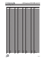
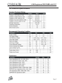
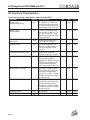
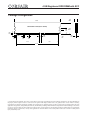
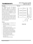
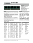
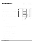
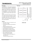
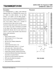
CM74SD4096RLP
4 GByte Registered DDR DIMM with ECC
Key Features
Error Checking and Correcting (ECC) for maximum memory
reliability
Ultra high density using 1024 MBit SDRAM devices
High Performance
-
registered synchronous Double Data Rate SDRAM
-
all inputs synchronized to system clock
-
data transferred on both rising and falling edge of clock
-
PLL-based clock regeneration
SSTL-2 compatible (2.5V) switching
Serial Presence Detect (SPD) EEPROM provides automatic memory
configuration
Series termination on clock and data lines
Board footprint of less than 2.0 square inches
Built using thirty-six 256M x 4 DDR SDRAMS, 8K refresh
Pin-compatible with all PC1600, PC2100, and PC2700 modules
Low Profile: 1.2 inches tall
Selection Guide
CM74SD4096RLP-xxxx/x
MODULE SIZE:
4 GBytes
ADDRESS PATH:
R = Registered
MODULE HEIGHT
LP = 1.2 inches
CORSAIR MEMORY
SPEED:
2700: PC2700 (333 MHz)
RAM VENDOR:
M = Micron
S = Samsung
www.corsairmemory.com
4 GB Registered DDR DIMM with ECC
General Description
The CM74SD4096RLP is a Double Data Rate SDRAM Dual Inline
Memory Module (DIMM), designed for applications requiring the ultimate
in memory density. This DIMM includes Error Checking and Correcting
(ECC) for maximum reliability, and has registered address and control
signals to enable fully configured systems.
These modules are constructed using thirty-six 256Mx4 (1024 MBit) DDR
SDRAMs in TSOP-II packages, and are fully compliant with appropriate
JEDEC specifications. The module also includes an EEPROM to support
Serial Presence Detect (SPD) requirements. Decoupling capacitors are
mounted on the printed circuit board for each DDR SDRAM device, and
series termination is provided on all clock and data lines.
The synchronous design of these Corsair SDRAM DIMMs allows precise
cycle control with the use of the system clock. Two I/O transactions are
possible on every clock cycle due to the use of double data rate RAMs. The
high clock frequency and high density of this device enable a high level of
performance to be achieved in advanced workstations and servers.
Pin Definitions
Pin Name
A0 - A13
BA0, BA1
DQ0 - DQ63
CB0 - CB7
DQS0 - DQS17
CK0, /CK0
CKE0, CKE1
/CS0, /CS1
/RAS
/CAS
/WE
VDD
VDDQ
VSS
VREF
VDDSPD
SDA
SCL
SA0 - SA2
/RESET
NC
Page 2
Function
Address Inputs
Bank Address Select Inputs
Data Input/Output
ECC Check Bits
Data Strobe Input/Output
Clock Inputs
Clock Enable Inputs
Chip Select Inputs
Row Address Strobe Input
Column Address Strobe Input
Write Enable Input
Power Supply (2.5V)
Data Input/Output Power Supply
Ground
SSTL-2 Signalling Reference Voltage
Serial EEPROM Power
SPD Data Output
SPD Clock Input
SPD Address Inputs
Reset Enable
No Connection
4 GB Registered DDR DIMM with ECC
Pin Configuration
Pin #
1
2
3
4
5
6
7
8
9
10
11
12
13
14
15
16
17
18
19
20
21
22
23
24
25
26
27
28
29
30
31
32
33
34
35
36
37
38
39
40
41
42
43
44
45
46
Front Side
VREF
DQ0
VSS
DQ1
DQS0
DQ2
VDD
DQ3
NC
/RESET
VSS
DQ8
DQ9
DQS1
VDDQ
NC
NC
VSS
DQ10
DQ11
CKE0
VDDQ
DQ16
DQ17
DQS2
VSS
A9
DQ18
A7
VDDQ
DQ19
A5
DQ24
VSS
DQ25
DQS3
A4
VDD
DQ26
DQ27
A2
VSS
A1
CB0
CB1
VDD
Pin #
93
94
95
96
97
98
99
100
101
102
103
104
105
106
107
108
109
110
111
112
113
114
115
116
117
118
119
120
121
122
123
124
125
126
127
128
129
130
131
132
133
134
135
138
137
138
Back Side
VSS
DQ4
DQ5
VDDQ
DQS9
DQ6
DQ7
VSS
NC
NC
NC
VDDQ
DQ12
DQ13
DQS10
VDD
DQ14
DQ15
CKE1
VDDQ
NC
DQ20
A12
VSS
DQ21
A11
DQS11
VDD
DQ22
A8
DQ23
VSS
A6
DQ28
DQ29
VDDQ
DQS12
A3
DQ30
VSS
DQ31
CB4
CB5
VDDQ
CK0
/CK0
Pin #
47
48
49
50
51
52
53
54
55
56
57
58
59
60
61
62
63
64
65
66
67
68
69
70
71
72
73
74
75
76
77
78
79
80
81
82
83
84
85
86
87
88
89
90
91
92
Front Side
DQS8
A0
CB2
VSS
CB3
BA1
DQ32
VDDQ
DQ33
DQS4
DQ34
VSS
BA0
DQ35
DQ40
VDDQ
/WE
DQ41
/CAS
VSS
DQS5
DQ42
DQ43
VDD
NC
DQ48
DQ49
VSS
NC
NC
VDDQ
DQS6
DQ50
DQ51
VSS
NC
DQ56
DQ57
VDD
DQS7
DQ58
DQ59
VSS
NC
SDA
SDL
Pin #
139
140
141
142
143
144
145
146
147
148
149
150
151
152
153
154
155
156
157
158
159
160
161
162
163
164
165
166
167
168
169
170
171
172
173
174
175
176
177
178
179
180
181
182
183
184
Back Side
VSS
DQS17
A10
CB6
VDDQ
CB7
VSS
DQ36
DQ37
VDD
DQS13
DQ38
DQ39
VSS
DQ44
/RAS
DQ45
VDDQ
/CS0
/CS1
DQS14
VSS
DQ46
DQ47
NC
VDDQ
DQ52
DQ53
A13
VDD
DQS15
DQ54
DQ55
VDDQ
NC
DQ60
DQ61
VSS
DQS16
DQ62
DQ63
VDDQ
SA0
SA1
SA2
VDDSPD
Page 3
4 GB Registered DDR DIMM with ECC
Functional Block Diagram
/CS1
/CS0
VSS
O
O
O
DQS0
DQ0
DQ1
DQ2
DQ3
O
O
O
O
O
DQS
DQ0
DQ1
DQ2
DQ3
DM
DQS9
DQ4
DQ5
DQ6
DQ7
O
O
O
O
O
DQS
DQ0
DQ1
DQ2
DQ3
DM
DQS1
DQ8
DQ9
DQ10
DQ11
O
O
O
O
O
DQS
DQ0
DQ1
DQ2
DQ3
DM
DQS10
DQ12
DQ13
DQ14
DQ15
O
O
O
O
O
DQS
DQ0
DQ1
DQ2
DQ3
DM
DQS8
CB0
CB1
CB2
CB3
O
O
O
O
O
DQS
DQ0
DQ1
DQ2
DQ3
DM
DQS2
DQ16
DQ17
DQ18
DQ19
O
O
O
O
O
DQS
DQ0
DQ1
DQ2
DQ3
DM
DQS11
DQ20
DQ21
DQ22
DQ23
O
O
O
O
O
DQS
DQ0
DQ1
DQ2
DQ3
DM
DQS3
DQ24
DQ25
DQ26
DQ27
O
O
O
O
O
DQS
DQ0
DQ1
DQ2
DQ3
DM
DQS12
DQ28
DQ29
DQ30
DQ31
O
O
O
O
O
DQS
DQ0
DQ1
DQ2
DQ3
DM
DQn o
/CS
U1a
/CS
U22a
/CS
U2a
/CS
U21a
/CS
U5a
/CS
U3a
/CS
U20a
/CS
U4a
/CS
U19a
DQS
DQ0
DQ1
DQ2
DQ3
DM
DQS
DQ0
DQ1
DQ2
DQ3
DM
DQS
DQ0
DQ1
DQ2
DQ3
DM
DQS
DQ0
DQ1
DQ2
DQ3
DM
DQS
DQ0
DQ1
DQ2
DQ3
DM
DQS
DQ0
DQ1
DQ2
DQ3
DM
DQS
DQ0
DQ1
DQ2
DQ3
DM
DQS
DQ0
DQ1
DQ2
DQ3
DM
DQS
DQ0
DQ1
DQ2
DQ3
DM
/CS
U1b
/CS
U22b
/CS
U2b
/CS
U21b
/CS
U5b
/CS
U3b
/CS
U20b
/CS
U4b
/CS
U19b
All SDRAMs
VDD
All SDRAMs
VREF
All SDRAMs
VSS
All SDRAMs
O
O
O
O
O
DQS
DQ0
DQ1
DQ2
DQ3
DM
DQS13
DQ36
DQ37
DQ38
DQ39
O
O
O
O
O
DQS
DQ0
DQ1
DQ2
DQ3
DM
DQS5
DQ40
DQ41
DQ42
DQ43
O
O
O
O
O
DQS
DQ0
DQ1
DQ2
DQ3
DM
DQS14
DQ44
DQ45
DQ46
DQ47
O
O
O
O
O
DQS
DQ0
DQ1
DQ2
DQ3
DM
DQS17
CB4
CB5
CB6
CB7
O
O
O
O
O
DQS
DQ0
DQ1
DQ2
DQ3
DM
DQS6
DQ48
DQ49
DQ50
DQ51
O
O
O
O
O
DQS
DQ0
DQ1
DQ2
DQ3
DM
DQS15
DQ52
DQ53
DQ54
DQ55
O
O
O
O
O
DQS
DQ0
DQ1
DQ2
DQ3
DM
DQS7
DQ56
DQ57
DQ58
DQ59
O
O
O
O
O
DQS
DQ0
DQ1
DQ2
DQ3
DM
DQS16
DQ60
DQ61
DQ62
DQ63
O
O
O
O
O
DQS
DQ0
DQ1
DQ2
DQ3
DM
A0 - A13
BA0, BA1
/RAS, /CAS
/WE
CKE0, CKE1
/CS0, /CS1
Every DQ
pin of
SDRAM
VDDQ
DQS4
DQ32
DQ33
DQ34
DQ35
/CS
U6a
/CS
U17a
/CS
U7a
/CS
U16a
/CS
U18a
/CS
U8a
/CS
U15a
/CS
U9a
/CS
U14a
DQS
DQ0
DQ1
DQ2
DQ3
DM
DQS
DQ0
DQ1
DQ2
DQ3
DM
DQS
DQ0
DQ1
DQ2
DQ3
DM
DQS
DQ0
DQ1
DQ2
DQ3
DM
DQS
DQ0
DQ1
DQ2
DQ3
DM
DQS
DQ0
DQ1
DQ2
DQ3
DM
DQS
DQ0
DQ1
DQ2
DQ3
DM
DQS
DQ0
DQ1
DQ2
DQ3
DM
DQS
DQ0
DQ1
DQ2
DQ3
DM
U6b
/CS
U17b
/CS
U7b
/CS
U16b
/CS
U18b
/CS
U8b
/CS
U15b
/CS
U9b
/CS
U14b
Reg
All SDRAMs
Serial PD
120 7
SCL
Page 4
/CS
CLK0
/CLK0
PLL
All SDRAMs
& registers
WP
A0 A1 A2
SA0 SA1 SA2
SDA
4 GB Registered DDR DIMM with ECC
DC Electrical Specifications
Page 5
4 GB Registered DDR DIMM with ECC
DC Electrical Characteristics
Over the operating range unless otherwise specified
Parameter
Symbol
Test Conditions
Min
Max
Unit
Operating Current One bank active precharge
IDD0
tRC = tRCmin; tCK = 133MHz, DQ,
DM, and DQS inputs changing twice
per clock cycle; Address and control
inputs changing once per clock cycle
4600
mA
Operating Current One bank operation
IDD1
One bank; Active-Read-Precharge;
Burst = 2; tRC = 133 MHz, CL = 2.5;
tCK = tRC =133 MHz; Iout = 0 mA;
Address and control inputs changing
once per clock cycle
5140
mA
Precharge Power-Down
Standby Current
IDD2P
All banks idle; Power-down mode;
CKE = LOW; tCK = 133 MHz
841
mA
Idle Standby Current
IDD2F
/CS = HIGH; All banks idle; CKE =
HIGH; tCK = 133MHz; Address and
control inputs changing once per
clock cycle
2260
mA
Active Power-Down Standby Current
IDD3P
One bank active; Power-down
mode;CKE = LOW; tCK = 133 MHz
1705
mA
Active Standby Current
IDD3N
/CS = HIGH; CKE = HIGH; One bank
active; Active-precharge; tRC =
tRASmax; tCK = 133MHz; DQ, DQM,
and DQS inputs changing twice per
clock cycle; Address and control
inputs changing once per clock cycle
3160
mA
Operating Current - Burst Read
IDD4R
Burst length = 2; Reads; Continuous
burst; One bank active; Address and
control inputs changing once per
clock cycle; CL = 2.5; tCK = 133MHz;
DQ, DQM, and DQS inputs changing
twice per clock cycle
5500
mA
Operating Current - Burst Write
IDD4W
Burst length = 2; Writes; Continuous
burst; One bank active; Address and
control inputs changing once per
clock cycle; CL = 2.5; tCK = 133MHz;
DQ, DQM, and DQS inputs changing
twice per clock cycle
6760
mA
tRC = tRFCmin
7480
mA
913
mA
Auto Refresh Current
IDD5
Self Refresh Current
IDD6
Page 6
4 GB Registered DDR DIMM with ECC
Package Configuration
.300
MAX
5.250
COMPONENT AREA (BOTH SIDES)
.700
TYP
1.200
MAX
.091
TYP
.250
TYP
Pin 1
.091
TYP
.040
TYP
.394
TYP
.050
TYP
2.55
.050
TYP
1.95
4.750
© Corsair Memory Incorporated, June, 2005. Corsair and the Corsair Logo are trademarks of Corsair Memory Incorporated. All other trademarks are
the property of their respective owners. Corsair reserves the right to make changes without notice to any products herein. Corsair makes no warranty,
representation, or guarantee regarding the suitability of its products for any particular purpose, nor does Corsair assume any liability arising out of the
application of any product, and specifically disclaims any and all liability, including without limitation consequential or incidental damages. Corsair does
not convey any license under its patent rights nor the rights of others. Corsair products are not designed, intended, or authorized for use in applications
intended to support or sustain life, or for any other application for which the failure of the Corsair product could create a situation in which personal
injury or death may occur.