1
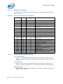
ACPI Devices
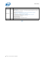
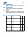
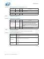
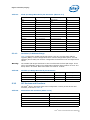
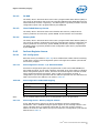
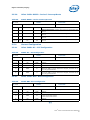
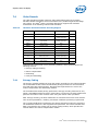
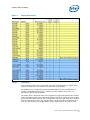
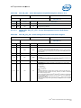
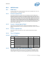
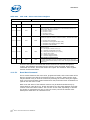
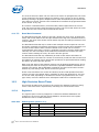
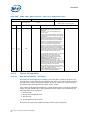
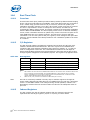
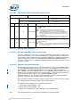
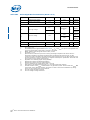
Table 385.
Flash Erase Time
Device
Erase Time (max)
Description
PMC* PM25LV
100 ms
Same for block or sector
Atmel* AT25F
1.1 s
SST* SST25VF
25, 25, 100 ms
Sector, block, chip
NexFlash* NX25P
2, 3/5 s
Sector, chip 2 mb/4 mb
ST* M25P80
3s
Sector
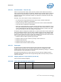
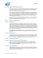
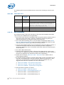
The Write process is executed to write bytes to the Flash device. The atomic
instructions that make up the Write process include a Write enable instruction, a Write
(or Program) instruction and finally a status poll.
Note that the Write Disable occurs automatically following the completion of the Write
opcode in nearly all cases. The processor does not support explicitly disabling writes as
part of the Atomic write sequence.
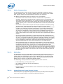
It is recommended that BIOS avoid using instructions that take more than one second
to complete inside the flash. See Section 11.9.5.12.1, for details.
11.9.7.1
Run Time Updates
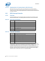
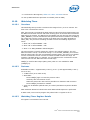
BIOS, especially SMI code, may log errors or record other run-time variables in a
section of the flash by writing a few bytes at a time. It is recommended that run time
updates be performed to a section of flash that has already been erased and allocated.
BIOS keeps a pointer to the next byte to be written and updates the pointer real time
as bytes are written. SMI# may optionally be enabled by performing a programmed
write with the SPI SMI# Enable bit set to report to software when the update has
completed.
Direct memory reads to the SPI flash can encounter long delays. The processor may
directly block progress of one or more threads in the system. Therefore, run-time reads
are recommended to use the programmed command mechanism and optionally the
Software-Based SPI Access Request/Grant mechanism. The programmed command
mechanism allows reads to the flash to be generated using posted writes. The
completion of the read can be determined by polling the SPI Status register (in the
processor) or by receiving an SMI#. With either method, the system is not
encountering long delays for a single non-postable cycle to complete on the front-side
bus. Host software can read the data out of the data registers when the cycle
completes.
11.9.7.2
BIOS Sector Updates
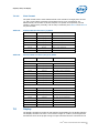
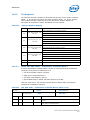
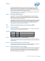
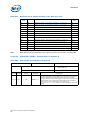
If a large sector of the Flash is to be updated, external SPI bus master will need to be
informed through the Future Req protocol to avoid long transactions. The process for
updating a sector varies from device to device, some devices will allow up to a 256 byte
write while others only allow a byte write at a time. From a processor point of view,
software should write up to 64 bytes at a time into the write posting buffer. Data that
needs to be preserved should be copied to scratch pad memory and copied in at the
respective address.
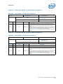
Software needs to be aware of different sector write algorithms between Flash vendors.
For example, SST* Flash does not allow 64 byte writes, it allows byte writes only.
Hardware does not split 64 byte writes from the posting buffer; it is software’s
responsibility to write byte by byte.
Intel® Atom™ Processor E6xx Series Datasheet
261