1
5th Generation Intel® Core™
Processor Family, Intel® Core™ M
Processor Family, Mobile Intel®
Pentium® Processor Family, and
Mobile Intel® Celeron® Processor
Family
Datasheet – Volume 1 of 2
March 2015
Order No.: 330834-004v1
You may not use or facilitate the use of this document in connection with any infringement or other legal analysis concerning Intel products described
herein. You agree to grant Intel a non-exclusive, royalty-free license to any patent claim thereafter drafted which includes subject matter disclosed
herein.
No license (express or implied, by estoppel or otherwise) to any intellectual property rights is granted by this document.
All information provided here is subject to change without notice. Contact your Intel representative to obtain the latest Intel product specifications and
roadmaps.
The products described may contain design defects or errors known as errata which may cause the product to deviate from published specifications.
Current characterized errata are available on request.
Copies of documents which have an order number and are referenced in this document may be obtained by calling 1-800-548-4725 or visit http://
www.intel.com/design/literature.htm.
Intel technologies’ features and benefits depend on system configuration and may require enabled hardware, software or service activation. Learn
more at http://www.intel.com/ or from the OEM or retailer.
No computer system can be absolutely secure.
Intel® Hyper-Threading Technology (Intel® HT Technology) is available on select Intel® Core™ processors. It requires an Intel® HT Technology enabled
system. Consult your PC manufacturer. Performance will vary depending on the specific hardware and software used. Not available on Intel® Core™
i5-750. For more information including details on which processors support Intel® HT Technology, visit http://www.intel.com/info/hyperthreading.
Intel® High Definition Audio (Intel® HD Audio) requires an Intel® HD Audio enabled system. Consult your PC manufacturer for more information.
Sound quality will depend on equipment and actual implementation. For more information about Intel® HD Audio, refer to http://www.intel.com/
design/chipsets/hdaudio.htm.
Intel® 64 architecture requires a system with a 64-bit enabled processor, chipset, BIOS and software. Performance will vary depending on the specific
hardware and software you use. Consult your PC manufacturer for more information. For more information, visit http://www.intel.com/
content/www/us/en/architecture-and-technology/microarchitecture/intel-64-architecture-general.html.
Intel® Virtualization Technology (Intel® VT) requires a computer system with an enabled Intel® processor, BIOS, and virtual machine monitor (VMM).
Functionality, performance or other benefits will vary depending on hardware and software configurations. Software applications may not be
compatible with all operating systems. Consult your PC manufacturer. For more information, visit http://www.intel.com/go/virtualization.
The original equipment manufacturer must provide TPM functionality, which requires a TPM-supported BIOS. TPM functionality must be initialized and
may not be available in all countries.
For Enhanced Intel SpeedStep® Technology, see the Processor Spec Finder at http://ark.intel.com/ or contact your Intel representative for more
information.
Intel® AES-NI requires a computer system with an AES-NI enabled processor, as well as non-Intel software to execute the instructions in the correct
sequence. AES-NI is available on select Intel® processors. For availability, consult your reseller or system manufacturer. For more information, see
http://software.intel.com/en-us/articles/intel-advanced-encryption-standard-instructions-aes-ni/.
Intel® Active Management Technology (Intel® AMT) should be used by a knowledgeable IT administrator and requires enabled systems, software,
activation, and connection to a corporate network. Intel AMT functionality on mobile systems may be limited in some situations. Your results will
depend on your specific implementation. Learn more by visiting Intel® Active Management Technology.
No computer system can provide absolute security under all conditions. Intel® Trusted Execution Technology (Intel® TXT) requires a computer with
Intel® Virtualization Technology, an Intel TXT-enabled processor, chipset, BIOS, Authenticated Code Modules and an Intel TXT-compatible measured
launched environment (MLE). Intel TXT also requires the system to contain a TPM v1.s. For more information, visit http://www.intel.com/technology/
security.
Requires a system with Intel® Turbo Boost Technology. Intel Turbo Boost Technology and Intel Turbo Boost Technology 2.0 are only available on select
Intel® processors. Consult your PC manufacturer. Performance varies depending on hardware, software, and system configuration. For more
information, visit https://www-ssl.intel.com/content/www/us/en/architecture-and-technology/turbo-boost/turbo-boost-technology.html.
Intel® Advanced Vector Extensions (Intel® AVX) are designed to achieve higher throughput to certain integer and floating point operations. Due to
varying processor power characteristics, utilizing AVX instructions may cause a) some parts to operate at less than the rated frequency and b) some
parts with Intel® Turbo Boost Technology 2.0 to not achieve any or maximum turbo frequencies. Performance varies depending on hardware, software,
and system configuration and you should consult your system manufacturer for more information. Intel® Advanced Vector Extensions refers to Intel®
AVX, Intel® AVX2 or Intel® AVX-512. For more information on Intel® Turbo Boost Technology 2.0, visit https://www-ssl.intel.com/content/www/us/en/
architecture-and-technology/turbo-boost/turbo-boost-technology.html
Intel, Intel Core, Celeron, Pentium, Intel SpeedStep, and the Intel logo are trademarks of Intel Corporation in the U.S. and/or other countries.
*Other names and brands may be claimed as the property of others.
Copyright
©
2014–2015, Intel Corporation. All rights reserved.
5th Generation Intel® Core™ Processor Family, Intel® Core™ M Processor Family, Mobile Intel® Pentium® Processor Family, and
Mobile Intel® Celeron® Processor Family
Datasheet – Volume 1 of 2
March 2015
2
Order No.: 330834-004v1
Contents—Processor
Contents
Revision History..................................................................................................................9
1.0 Introduction................................................................................................................10
1.1
1.2
1.3
1.4
1.5
1.6
1.7
Supported Technologies.........................................................................................11
Power Management Support...................................................................................12
Thermal Management Support................................................................................12
Package Support...................................................................................................13
Processor Testability............................................................................................. 13
Terminology.........................................................................................................13
Related Documents............................................................................................... 16
2.0 Interfaces................................................................................................................... 18
2.1 System Memory Interface...................................................................................... 18
2.1.1 System Memory Technology Supported ......................................................18
2.1.2 System Memory Timing Support................................................................. 19
2.1.3 Intel® Fast Memory Access (Intel® FMA)..................................................... 20
2.1.4 System Memory Frequency........................................................................ 21
2.1.5 System Memory Organization Modes ......................................................... 21
2.1.6 Data Scrambling...................................................................................... 22
2.2 Processor Graphics................................................................................................22
2.3 Processor Graphics Controller (GT)..........................................................................23
2.3.1 3D and Video Engines for Graphics Processing.............................................. 23
2.4 Digital Display Interface (DDI)................................................................................25
2.5 Platform Environmental Control Interface (PECI)....................................................... 31
2.5.1 PECI Bus Architecture................................................................................31
3.0 Technologies............................................................................................................... 33
3.1 Intel® Virtualization Technology (Intel® VT)............................................................. 33
3.2 Intel® Trusted Execution Technology (Intel® TXT)..................................................... 37
3.3 Intel® Hyper-Threading Technology (Intel® HT Technology)....................................... 38
3.4 Intel® Turbo Boost Technology 2.0..........................................................................39
3.5 Intel® Advanced Vector Extensions 2.0 (Intel® AVX2)................................................39
3.6 Intel® Advanced Encryption Standard New Instructions (Intel® AES-NI).......................39
3.7 Intel® 64 Architecture x2APIC................................................................................ 40
3.8 Power Aware Interrupt Routing (PAIR).................................................................... 42
3.9 Execute Disable Bit............................................................................................... 42
3.10 Intel® Device Protection with Boot Guard............................................................... 42
3.11 Supervisor Mode Execution Protection (SMEP)........................................................42
3.12 Supervisor Mode Access Protection (SMAP) ........................................................... 43
3.13 Intel® Transactional Synchronization Extensions - New Instructions (Intel® TSX-NI)... 43
4.0 Power Management.................................................................................................... 44
4.1 Advanced Configuration and Power Interface (ACPI) States Supported......................... 45
4.2 Processor Core Power Management......................................................................... 46
4.2.1 Enhanced Intel® SpeedStep® Technology Key Features..................................46
4.2.2 Low-Power Idle States............................................................................... 47
4.2.3 Requesting Low-Power Idle States...............................................................48
4.2.4 Core C-State Rules....................................................................................48
5th Generation Intel® Core™ Processor Family, Intel® Core™ M Processor Family, Mobile Intel® Pentium® Processor Family, and
Mobile Intel® Celeron® Processor Family
March 2015
Datasheet – Volume 1 of 2
Order No.: 330834-004v1
3
Processor—Contents
4.2.5 Package C-States......................................................................................50
4.2.6 Package C-States and Display Resolutions.................................................... 53
4.3 Integrated Memory Controller (IMC) Power Management............................................54
4.3.1 Disabling Unused System Memory Outputs................................................... 55
4.3.2 DRAM Power Management and Initialization..................................................55
4.3.3 DDR Electrical Power Gating (EPG).............................................................. 57
4.4 Graphics Power Management..................................................................................58
4.4.1 Intel® Rapid Memory Power Management (Intel® RMPM)................................58
4.4.2 Graphics Render C-State............................................................................58
4.4.3 Intel® Smart 2D Display Technology (Intel® S2DDT)..................................... 58
4.4.4 Intel® Graphics Dynamic Frequency............................................................ 58
4.4.5 Intel® Display Power Saving Technology (Intel® DPST)................................. 59
4.4.6 Intel® Automatic Display Brightness ........................................................... 59
4.4.7 Intel® Seamless Display Refresh Rate Technology (Intel® SDRRS
Technology)............................................................................................ 59
5.0 Thermal Management................................................................................................. 60
5.1 Thermal Considerations......................................................................................... 60
5.2 Intel® Turbo Boost Technology 2.0 Power Monitoring.................................................61
5.3 Intel® Turbo Boost Technology 2.0 Power Control..................................................... 61
5.3.1 Package Power Control.............................................................................. 61
5.3.2 Turbo Time Parameter............................................................................... 62
5.4 Configurable TDP (cTDP) and Low-Power Mode......................................................... 62
5.4.1 Configurable TDP...................................................................................... 63
5.4.2 Low-Power Mode.......................................................................................63
5.5 Thermal and Power Specifications........................................................................... 64
5.6 Thermal Management Features............................................................................... 66
5.6.1 Adaptive Thermal Monitor.......................................................................... 66
5.6.2 Digital Thermal Sensor.............................................................................. 68
5.6.3 PROCHOT# Signal.....................................................................................69
5.6.4 On-Demand Mode..................................................................................... 70
5.6.5 Intel® Memory Thermal Management.......................................................... 71
6.0 Signal Description....................................................................................................... 72
6.1 System Memory Interface Signals........................................................................... 72
6.2 Memory Compensation and Miscellaneous Signals..................................................... 74
6.3 Reset and Miscellaneous Signals............................................................................. 74
6.4 embedded DisplayPort* (eDP*) Signals....................................................................75
6.5 Display Interface Signals....................................................................................... 75
6.6 Testability Signals.................................................................................................75
6.7 Error and Thermal Protection Signals....................................................................... 76
6.8 Power Sequencing Signals......................................................................................77
6.9 Processor Power Signals........................................................................................ 77
6.10 Sense Signals..................................................................................................... 78
6.11 Ground and Non-Critical to Function (NCTF) Signals.................................................78
6.12 Processor Internal Pull-Up / Pull-Down Terminations................................................ 79
7.0 Electrical Specifications.............................................................................................. 80
7.1
7.2
7.3
7.4
Integrated Voltage Regulator..................................................................................80
Power and Ground Pins..........................................................................................80
VCC Voltage Identification (VID).............................................................................. 80
Reserved or Unused Signals................................................................................... 85
5th Generation Intel® Core™ Processor Family, Intel® Core™ M Processor Family, Mobile Intel® Pentium® Processor Family, and
Mobile Intel® Celeron® Processor Family
Datasheet – Volume 1 of 2
March 2015
4
Order No.: 330834-004v1
Contents—Processor
7.5
7.6
7.7
7.8
Signal Groups.......................................................................................................85
Test Access Port (TAP) Connection.......................................................................... 87
DC Specifications................................................................................................. 87
Voltage and Current Specifications.......................................................................... 87
7.8.1 Platform Environment Control Interface (PECI) DC Characteristics................... 94
7.8.2 Input Device Hysteresis............................................................................. 95
8.0 Package Specifications................................................................................................96
8.1 Package Mechanical Attributes................................................................................ 96
8.2 Package Loading Specifications............................................................................... 97
8.3 Package Storage Specifications............................................................................... 97
9.0 Processor Ball and Signal Information........................................................................ 98
9.1 Intel® Core™ M Processor Family Ball Information (BGA1234)..................................... 98
9.2 U-Processor Ball Information (BGA1168)................................................................ 111
5th Generation Intel® Core™ Processor Family, Intel® Core™ M Processor Family, Mobile Intel® Pentium® Processor Family, and
Mobile Intel® Celeron® Processor Family
March 2015
Datasheet – Volume 1 of 2
Order No.: 330834-004v1
5
Processor—Figures
Figures
1
2
3
4
5
6
7
8
9
10
11
12
13
Processor Platform Block Diagram..............................................................................11
Intel® Flex Memory Technology Operations................................................................. 22
Processor Display Architecture ..................................................................................26
DisplayPort* Overview............................................................................................. 27
HDMI* Overview..................................................................................................... 28
PECI Host-Clients Connection Example....................................................................... 32
Device to Domain Mapping Structures........................................................................ 36
Processor Power States............................................................................................ 44
Processor Package and Core C-States.........................................................................45
Idle Power Management Breakdown of the Processor Cores .......................................... 47
Package C-State Entry and Exit................................................................................. 51
Package Power Control............................................................................................. 62
Input Device Hysteresis............................................................................................95
5th Generation Intel® Core™ Processor Family, Intel® Core™ M Processor Family, Mobile Intel® Pentium® Processor Family, and
Mobile Intel® Celeron® Processor Family
Datasheet – Volume 1 of 2
March 2015
6
Order No.: 330834-004v1
Tables—Processor
Tables
1
2
3
4
5
6
7
8
9
10
11
12
13
14
15
16
17
18
19
20
21
22
23
24
25
26
27
28
29
30
31
32
33
34
35
36
37
38
39
40
41
42
43
44
45
46
47
48
49
50
51
Terminology........................................................................................................... 13
Related Documents..................................................................................................16
Processor DIMM Support Summary By Product............................................................ 18
Supported DDR3L / DDR3L-RS SO-DIMM Module Configurations Per Channel...................19
Supported DDR3L/DDR3L-RS Memory Down Configurations Per Channel......................... 19
Supported LPDDR3 Memory Down Configurations Per Channel....................................... 19
DRAM System Memory Timing Support.......................................................................20
Processor Supported Audio Formats over HDMI*and DisplayPort*.................................. 28
Multiple Display Configuration for 5th Generation Intel® Core™ Processor Family,
Mobile Intel® Pentium® Processor Family, and Mobile Intel® Celeron® Processor Family....29
Multiple Display Configuration for Intel® Core™ M Processor Family................................ 30
DisplayPort and embedded DisplayPort* Resolutions for 1, 2, 4 Lanes – Link Data
Rate of RBR, HBR, and HBR2 for U-Processor Line........................................................30
DisplayPort and embedded DisplayPort* Resolutions for 1, 2, 4 Lanes – Link Data
Rate of RBR, HBR, and HBR2 for Intel® Core™ M Processor Family................................. 31
System States.........................................................................................................45
Processor Core / Package State Support..................................................................... 45
Integrated Memory Controller States..........................................................................46
G, S, and C Interface State Combinations .................................................................. 46
Coordination of Core Power States at the Package Level............................................... 51
Package C-States and Display Resolutions.................................................................. 54
Targeted Memory State Conditions............................................................................ 57
Configurable TDP Modes........................................................................................... 63
Thermal Design Power (TDP) Specifications.................................................................65
Junction Temperature Specification............................................................................ 65
Idle Power Specification............................................................................................66
Signal Description Buffer Types................................................................................. 72
DDR3L / DDR3L-RS Memory Down Channel A and B Memory Signals.............................. 72
LPDDR3 Memory Down Channel A and B Memory Signals.............................................. 73
LPDDR3 / DDR3L / DDR3L-RS Reference and Compensation Signals............................... 74
Reset and Miscellaneous Signals................................................................................ 74
embedded Display Port* Signals................................................................................ 75
Display Interface Signals.......................................................................................... 75
Testability Signals....................................................................................................75
Error and Thermal Protection Signals..........................................................................76
Power Sequencing Signals........................................................................................ 77
Processor Power Signals........................................................................................... 77
Sense Signals......................................................................................................... 78
Ground and Non-Critical to Function (NCTF) Signals..................................................... 78
Processor Internal Pull-Up / Pull-Down Terminations.................................................... 79
Voltage Regulator (VR) 12.5 Voltage Identification....................................................... 81
Signal Groups......................................................................................................... 85
Processor Core Active and Idle Mode DC Voltage and Current Specifications.................... 87
Memory Controller (VDDQ) Supply DC Voltage and Current Specifications.........................89
Vcc Sustain (VccST) Supply DC Voltage and Current Specifications..................................89
DDR3L / DDR3L-RS Signal Group DC Specifications......................................................89
LPDDR3 Signal Group DC Specifications......................................................................91
Digital Display Interface Group DC Specifications......................................................... 93
Embedded DisplayPort* (eDP) Group DC Specifications.................................................93
CMOS Signal Group DC Specifications.........................................................................93
GTL Signal Group and Open Drain Signal Group DC Specifications.................................. 93
VR Enable CMOS Signal Group DC Specification........................................................... 94
VCOMP_OUT and VCCIO_TERM .................................................................................94
Platform Environment Control Interface (PECI) DC Electrical Limits................................ 94
5th Generation Intel® Core™ Processor Family, Intel® Core™ M Processor Family, Mobile Intel® Pentium® Processor Family, and
Mobile Intel® Celeron® Processor Family
March 2015
Datasheet – Volume 1 of 2
Order No.: 330834-004v1
7
Processor—Tables
52
53
54
55
56
57
Package Mechanical Attributes...................................................................................96
Package Loading Specifications..................................................................................97
Package Storage Specifications..................................................................................97
Intel® Core™ M Processor Family (LP-DDR3, Non-Interleaved)....................................... 98
U-Processor Ball Information (DDR3, Non-Interleaved) .............................................. 111
U-Processor Ball Information (LP-DDR3, Non-Interleaved) .......................................... 123
5th Generation Intel® Core™ Processor Family, Intel® Core™ M Processor Family, Mobile Intel® Pentium® Processor Family, and
Mobile Intel® Celeron® Processor Family
Datasheet – Volume 1 of 2
March 2015
8
Order No.: 330834-004v1
Revision History—Processor
Revision History
Revision
001
Description
•
•
January 2015
•
•
Updated Table 21, Thermal Design Power (TDP) Specifications
Updated Table 40, Processor Core Active and Idle Mode DC
Voltage and Current Specifications. Note 3 is added to
"Operating voltage" row and "Idle voltage" row.
January 2015
•
Added 5th Generation Intel® Core™ processors i3-5020U and
i3-5015U
Added Intel® Pentium® processor 3825U
March 2015
•
•
•
•
•
•
•
•
•
•
•
•
003
September 2014
Intel®
Added
Transactional Synchronization Extensions - New
Instructions (Intel® TSX-NI)
Minor Updates throughout for clarity.
Added 5th Generation Intel® Core™ Processor Family
Added Intel® Pentium® processor family
Added Intel® Celeron® processor family
AddedIntel® Core™ M processor 5Y71, 5Y51, 5Y31, and 5Y10C
processors
Updated Section 2.1, System Memory Interface
Updated Section 2.1.1, System Memory Technology Supported
Added Section 2.1.2, System Memory Timing Support
Added Section 2.1.4, System Memory Frequency
Updated Table 9, Multiple Display Configuration for Intel®
Core™ M Processor
Updated Section 4.3.4, Package C-States. Added sentence to
Package C7 State sub-section.
Added Section 4.2.6, Package C-States and Display Resolutions
Updated Section 5.5, Thermal and Power Specifications
Updated Section 6.11, Ground and Non-Critical to Function
(NCTF) Signals. Added package type to Signal Name.
Updated Section 6.12, Processor Internal Pull-Up / Pull-Down
Terminations. Added table note.
Updated Table 36, Processor Core Active and Idle Mode DC
Voltage and Current Specifications
Added Chapter 9, Processor Ball and Signal Information
•
•
•
•
•
002
Initial Release
Date
004
•
5th Generation Intel® Core™ Processor Family, Intel® Core™ M Processor Family, Mobile Intel® Pentium® Processor Family, and
Mobile Intel® Celeron® Processor Family
March 2015
Datasheet – Volume 1 of 2
Order No.: 330834-004v1
9
Processor—Introduction
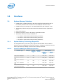
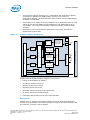
1.0
Introduction
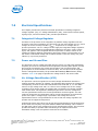
The 5th Generation Intel® Core™ processor family based on U-Processor line, Intel®
Core™ M processor family, Mobile Intel® Pentium® processor family, and Mobile Intel®
Celeron® processor family are 64-bit, multi-core processors built on 14-nanometer
process technology.
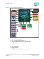
The processors are designed for a one-chip platform that includes a low-power
Platform Controller Hub (PCH) die in the same package as the processor die. The PCH
is referred to as the The Mobile 5th Generation Intel® Core™ Processor Family I/O,
Intel® Core™ M processor family I/O, Mobile Intel® Pentium® Processor Family I/O,
and Mobile Intel® Celeron® Processor Family I/O. Refer to the Related Documents
section for PCH document information. See the following figure for the processor
platform block diagram.
Throughout this document, the 5th Generation Intel® Core™ processor fanily based on
U-Processor Line, Intel® Core™ M processor. Mobile Intel® Pentium® processor family,
and Mobile Intel® Celeron® processor family may be referred to simply as "processor".
Throughout this document, the 5th Generation Intel® Core™ processor family based
on U-Processor Line, Mobile Intel® Pentium® processor family, and Mobile Intel®
Celeron® processor family, may be referred to simply as "U-Processor Line".
Throughout this document, the Intel® Core™ M processor family refers to the 5Y71,
5Y51, 5Y31, 5Y70, 5Y10, 5Y10C, and 5Y10A processors.
Throughout this document, the 5th Generation Intel® Core™ processor family based
on the U-Processor Line refers to the i7-5600U, i7-5500U, i5-5300U, i5-5200U,
i3-5020U, i3-5015U, i3-5010U, i3-5005U, i7-5650U, i7-5550U, i5-5350U, i5-5250U,
i7-5557U, i5-5287U, i5-5257U, i3-5157U processors.
Throughout this document, the Mobile Intel® Pentium® processor family refers to the
3825U, 3805U processor.
Throughout this document, the Mobile Intel® Celeron® processor family refers to the
3755U and 3205U processors.
Refer to the processor Specification Update document for additional SKU details.
5th Generation Intel® Core™ Processor Family, Intel® Core™ M Processor Family, Mobile Intel® Pentium® Processor Family, and
Mobile Intel® Celeron® Processor Family
Datasheet – Volume 1 of 2
March 2015
10
Order No.: 330834-004v1
Introduction—Processor
Figure 1.
Processor Platform Block Diagram
DDR3L/LPDDR3
DDR Ch.A
Digital Display
Interface x 2
DDIx2
DDR Ch.B
Embedded Display Port
Cameras
BIOS/FW Flash
eDP
SATA
USB 2.0
USB 2.0/3.0
SPI
HDA/I2S
Gyro
USB 2.0
I2C, UART or USB
GPIO
GPS
USB 2.0/3.0 Ports
HD Audio Codec
EC
SDIO
Fingerprint Sensor
PECI
SMBUS
SMBUS 2.0
Touch Screen
I2C*
USB 2.0
SPI
PCI Express* 2.0 x8
TPM
SSD Drive
BT/3G/4G
WiFi / WiMax
Gigabit Network
Connection
NFC
Touch Pad
Sensors Hub
SD Slot
Magnetometer
Accelometer
Ambient Light
Sensor
1.1
Supported Technologies
•
Intel® Virtualization Technology (Intel® VT)
•
Intel® Active Management Technology 10.0 (Intel® AMT 10)
•
Intel® Trusted Execution Technology (Intel® TXT)
•
Intel® Streaming SIMD Extensions 4.2 (Intel® SSE4.2)
•
Intel® Hyper-Threading Technology (Intel® HT Technology)
•
Intel® 64 Architecture
•
Execute Disable Bit
•
Intel® Turbo Boost Technology 2.0
•
Intel® Advanced Vector Extensions 2.0 (Intel® AVX2)
5th Generation Intel® Core™ Processor Family, Intel® Core™ M Processor Family, Mobile Intel® Pentium® Processor Family, and
Mobile Intel® Celeron® Processor Family
March 2015
Datasheet – Volume 1 of 2
Order No.: 330834-004v1
11
Processor—Introduction
•
Intel® Device Protection Technology with Intel® Advanced Encryption Standard
New Instructions (Intel® AES-NI)
•
PCLMULQDQ Instruction
•
Intel® Device Protection Technology with Intel® Secure Key
•
Intel® Transactional Synchronization Extensions - New Instructions (Intel® TSXNI)
•
PAIR – Power Aware Interrupt Routing
•
SMEP – Supervisor Mode Execution Protection
•
SMAP – Supervisor Mode Access Protection
•
Enhanced Intel® Speedstep® Technology
•
Intel® Device Protection Technology with Boot Guard
•
DRAM Bit-Error Recovery (DBER)
Note:
The availability of the features may vary between processor SKUs.
1.2
Power Management Support
Processor Core
•
Full support of ACPI C-states as implemented by the following processor C-states:
—
•
C0, C1, C1E, C3, C6, C7, C8, C9, C10
Enhanced Intel SpeedStep® Technology
System
•
S0, S3, S4, S5
Memory Controller
•
Conditional self-refresh
•
Dynamic power-down
Processor Graphics Controller
1.3
•
Intel® Rapid Memory Power Management (Intel® RMPM)
•
Intel® Smart 2D Display Technology (Intel® S2DDT)
•
Graphics Render C-state (RC6)
•
Intel® Seamless Display Refresh Rate Switching with eDP port
•
Intel® Display Power Saving Technology (Intel® DPST)
Thermal Management Support
•
Digital Thermal Sensor
•
Adaptive Thermal Monitor
•
THERMTRIP# and PROCHOT# support
•
On-Demand Mode
5th Generation Intel® Core™ Processor Family, Intel® Core™ M Processor Family, Mobile Intel® Pentium® Processor Family, and
Mobile Intel® Celeron® Processor Family
Datasheet – Volume 1 of 2
March 2015
12
Order No.: 330834-004v1
Introduction—Processor
1.4
•
Memory Open and Closed Loop Throttling
•
Memory Thermal Throttling
•
External Thermal Sensor (TS-on-DIMM and TS-on-Board)
•
Render Thermal Throttling
•
Fan speed control with DTS
Package Support
The 5th Generation Intel® Core™ processor family based on U-Processor Line, Mobile
Intel® Pentium processor family, and Mobile Intel® Celeron® processor family are
available in the following package:
•
40 mm x 24 mm x 1.284 mm BGA package (BGA1168)
The Intel® Core™ M processor is available in the following package:
•
1.5
30 mm x 16.5 mm x 1.05 mm BGA package (BGA1234)
Processor Testability
The processor includes boundary-scan for board and system level testability.
1.6
Terminology
Table 1.
Terminology
Term
Description
APD
Active Power-down
B/D/F
Bus/Device/Function
BGA
Ball Grid Array
BLC
Backlight Compensation
BLT
Block Level Transfer
BMP
Binary Modification Program
BPP
Bits per pixel
CKE
Clock Enable
CLTM
Closed Loop Thermal Management
DDI
Digital Display Interface
DDR3
Third-generation Double Data Rate SDRAM memory technology
DDR3L
DDR3 Low Voltage
DDR3L-RS
DDR3 Low Voltage Reduced Standby Power
DLL
Delay-Locked Loop
DMA
Direct Memory Access
DP
DisplayPort*
DTS
Digital Thermal Sensor
continued...
5th Generation Intel® Core™ Processor Family, Intel® Core™ M Processor Family, Mobile Intel® Pentium® Processor Family, and
Mobile Intel® Celeron® Processor Family
March 2015
Datasheet – Volume 1 of 2
Order No.: 330834-004v1
13
Processor—Introduction
Term
Description
DVI*
Digital Visual Interface. DVI* is the interface specified by the DDWG (Digital Display
Working Group)
EC
Embedded Controller
ECC
Error Correction Code
eDP*
embedded DisplayPort*
EPG
Electrical Power Gating
EU
Execution Unit
FMA
Floating-point fused Multiply Add instructions
FSC
Fan Speed Control
HDCP
High-bandwidth Digital Content Protection
HDMI*
High Definition Multimedia Interface
HFM
High Frequency Mode
iDCT
Inverse Discrete Cosine Transform
IHS
Integrated Heat Spreader
GFX
Graphics
GUI
Graphical User Interface
IMC
Integrated Memory Controller
Intel® 64
Technology
64-bit memory extensions to the IA-32 architecture
Intel® DPST
Intel Display Power Saving Technology
Intel® TSX-NI
Intel Transactional Synchronization Extensions - New Instructions
Intel® TXT
Intel Trusted Execution Technology
Intel® VT
Intel Virtualization Technology. Processor virtualization, when used in conjunction
with Virtual Machine Monitor software, enables multiple, robust independent software
environments inside a single platform.
Intel®
Intel Virtualization Technology (Intel VT) for Directed I/O. Intel VT-d is a hardware
assist, under system software (Virtual Machine Manager or OS) control, for enabling
I/O device virtualization. Intel VT-d also brings robust security by providing protection
from errant DMAs by using DMA remapping, a key feature of Intel VT-d.
VT-d
IOV
I/O Virtualization
ISI
Inter-Symbol Interference
ITPM
Integrated Trusted Platform Module
LFM
Low Frequency Mode. LFM is Pn in the P-state table. It can be read at MSR CEh
[47:40].
LFP
Local Flat Panel
LPDDR3
Low-Power Third-generation Double Data Rate SDRAM memory technology
MCP
Multi-Chip Package
MFM
Minimum Frequency Mode. MFM is the minimum ratio supported by the processor and
can be read from MSR CEh [55:48].
MLE
Measured Launched Environment
continued...
5th Generation Intel® Core™ Processor Family, Intel® Core™ M Processor Family, Mobile Intel® Pentium® Processor Family, and
Mobile Intel® Celeron® Processor Family
Datasheet – Volume 1 of 2
March 2015
14
Order No.: 330834-004v1
Introduction—Processor
Term
Description
MLC
Mid-Level Cache
MSI
Message Signaled Interrupt
MSL
Moisture Sensitive Labeling
MSR
Model Specific Registers
NCTF
Non-Critical to Function. NCTF locations are typically redundant ground or non-critical
reserved, so the loss of the solder joint continuity at end of life conditions will not
affect the overall product functionality.
ODT
On-Die Termination
OLTM
Open Loop Thermal Management
PCG
Platform Compatibility Guide (PCG) (previously known as FMB) provides a design
target for meeting all planned processor frequency requirements.
PCH
Platform Controller Hub. The chipset with centralized platform capabilities including
the main I/O interfaces along with display connectivity, audio features, power
management, manageability, security, and storage features.
PECI
The Platform Environment Control Interface (PECI) is a one-wire interface that
provides a communication channel between Intel processor and chipset components
to external monitoring devices.
PL1, PL2
Power Limit 1 and Power Limit 2
PPD
Pre-charge Power-down
Processor
The 64-bit multi-core component (package)
Processor Core
The term “processor core” refers to Si die itself, which can contain multiple execution
cores. Each execution core has an instruction cache, data cache, and 256-KB L2
cache. All execution cores share the L3 cache.
Processor Graphics
Intel Processor Graphics
Rank
A unit of DRAM corresponding to four to eight devices in parallel, ignoring ECC. These
devices are usually, but not always, mounted on a single side of a SO-DIMM.
SCI
System Control Interrupt. SCI is used in the ACPI protocol.
SDP
Scenario Design Power
SF
Strips and Fans
SMM
System Management Mode
SMX
Safer Mode Extensions
Storage Conditions
A non-operational state. The processor may be installed in a platform, in a tray, or
loose. Processors may be sealed in packaging or exposed to free air. Under these
conditions, processor landings should not be connected to any supply voltages, have
any I/Os biased, or receive any clocks. Upon exposure to “free air” (that is, unsealed
packaging or a device removed from packaging material), the processor must be
handled in accordance with moisture sensitivity labeling (MSL) as indicated on the
packaging material.
SVID
Serial Voltage Identification
TAC
Thermal Averaging Constant
TAP
Test Access Point
TCASE
The case temperature of the processor, measured at the geometric center of the topside of the TTV IHS.
TCC
Thermal Control Circuit
continued...
5th Generation Intel® Core™ Processor Family, Intel® Core™ M Processor Family, Mobile Intel® Pentium® Processor Family, and
Mobile Intel® Celeron® Processor Family
March 2015
Datasheet – Volume 1 of 2
Order No.: 330834-004v1
15
Processor—Introduction
Term
Description
TCONTROL
TCONTROL is a static value that is below the TCC activation temperature and used as a
trigger point for fan speed control. When DTS > TCONTROL, the processor must comply
to the TTV thermal profile.
TDP
Thermal Design Power: Thermal solution should be designed to dissipate this target
power level. TDP is not the maximum power that the processor can dissipate.
TLB
Translation Look-aside Buffer
TTV
Thermal Test Vehicle. A mechanically equivalent package that contains a resistive
heater in the die to evaluate thermal solutions.
TM
Thermal Monitor. A power reduction feature designed to decrease temperature after
the processor has reached its maximum operating temperature.
VCC
Processor core power supply
VDDQ
DDR3L and LPDDR3 power supply.
VF
Vertex Fetch
VID
Voltage Identification
VS
Vertex Shader
VLD
Variable Length Decoding
VMM
Virtual Machine Monitor
VR
Voltage Regulator
VSS
Processor ground
1.7
Related Documents
Table 2.
Related Documents
Document
Document
Number /
Location
The 5th Generation Intel® Core™ Processor Family, Intel® Core™ M Processor Family,
Mobile Intel® Pentium® Processor Family, and Mobile Intel® Celeron® Processor
Family Datasheet, Volume 2 of 2
330835
The 5th Generation Intel® Core™ Processor Family, Intel® Core™ M Processor Family,
Mobile Intel® Pentium® Processor Family, and Mobile Intel® Celeron® Processor
Family Specification Update
330836
The 5th Generation Intel® Core™ Processor Family I/O, Intel® Core™ M Processor
Family I/O, Mobile Intel® Pentium® Processor Family I/O, and Mobile Intel® Celeron®
Processor Family I/O Datasheet
330837
The 5th Generation Intel® Core™ Processor Family I/O, Intel® Core™ M Processor
Family I/O, Mobile Intel® Pentium® Processor Family I/O, and Mobile Intel® Celeron®
Processor Family I/O Specification Update
330838
Advanced Configuration and Power Interface 3.0
http://
www.acpi.info/
continued...
5th Generation Intel® Core™ Processor Family, Intel® Core™ M Processor Family, Mobile Intel® Pentium® Processor Family, and
Mobile Intel® Celeron® Processor Family
Datasheet – Volume 1 of 2
March 2015
16
Order No.: 330834-004v1
Introduction—Processor
Document
Document
Number /
Location
DDR3 SDRAM Specification
http://
www.jedec.org
DisplayPort* Specification
http://
www.vesa.org
Intel® 64 and IA-32 Architectures Software Developer's Manuals
http://
www.intel.com/
products/processor/
manuals/index.htm
5th Generation Intel® Core™ Processor Family, Intel® Core™ M Processor Family, Mobile Intel® Pentium® Processor Family, and
Mobile Intel® Celeron® Processor Family
March 2015
Datasheet – Volume 1 of 2
Order No.: 330834-004v1
17
Processor—Interfaces
2.0
Interfaces
2.1
System Memory Interface
2.1.1
•
LPDDR3 down or DDR3L/DDR3L-RS Non-ECC Unbuffered Small Outline Dual InLine Memory Modules with a maximum of one DIMM per channel or down
•
LPDDR3 memory I/O Voltage of 1.2V. DDR3L/DDR3L-RS I/O Voltage of 1.35V
•
Two memory channels. Single-channel and dual-channel memory organization
modes
•
64-bit wide channels
•
Data burst length of eight for all memory organization modes
•
Theoretical maximum memory bandwidth of:
—
21.3 GB/s in dual-channel mode assuming 1333 MT/s
—
25.6 GB/s in dual-channel mode assuming 1600 MT/s
—
29.8 GB/s in dual-channel mode assuming 1866 MT/s
System Memory Technology Supported
The Integrated Memory Controller (IMC) supports DDR3L/DDR3L-RS and LPDDR3
protocols with two independent, 64-bit wide channels. It supports unbuffered non-ECC
memory per channel, allowing up to two device ranks per channel.
Table 3.
Processor DIMM Support Summary By Product
Processor Type
TDP (W)
Graphics
Configurat
ion
DIMM Per
Channel
Memory Speed
DDR3L /
DDR3L-RS
(MT/s)
LPDDR3
(MT/s)
Intel® Core™ M Processor
6
GT2
1
1333, 1600
1333, 1600
Intel® Core™ U-Processor
Line
28
GT3
1
1333, 1600
1600, 1866
Intel® Core™ U-Processor
Line
15
GT3
1
1333, 1600
1600, 1866
Intel® Core™ U-Processor
Line
15
GT2
1
1333, 1600
1333, 1600
Intel® Pentium® Processor
Intel® Celeron® Processor
15
GT1
1
1333, 1600
1333, 1600
5th Generation Intel® Core™ Processor Family, Intel® Core™ M Processor Family, Mobile Intel® Pentium® Processor Family, and
Mobile Intel® Celeron® Processor Family
Datasheet – Volume 1 of 2
March 2015
18
Order No.: 330834-004v1
Interfaces—Processor
Table 4.
Table 5.
Supported DDR3L / DDR3L-RS SO-DIMM Module Configurations Per Channel
Raw
Card
Version
SODIMM
Capacity
SDRAM
Organizati
on
SDRAM
Density
# of
SDRAM
Devices
# of
Ranks
# of
Row/Col
Address
Bits
# of
SDRAM
Banks
Page Size
A
2 GB
128 M x 16
2 Gb
8
2
14/10
8
8 KB
A
4 GB
256 M x 16
4 Gb
8
2
15/10
8
8 KB
B
2 GB
256 M x 8
2 Gb
8
1
15/10
8
8 KB
B
4 GB
512 M x 8
4 Gb
8
1
16/10
8
8 KB
C
1 GB
128 M x16
2 Gb
4
1
14/10
8
8 KB
C
2 GB
256 M x16
4 Gb
4
1
15/10
8
8 KB
F
4 GB
256 M x8
2 Gb
16
2
15/10
8
8 KB
F
8 GB
512 M x8
4 Gb
16
2
16/10
8
8 KB
Supported DDR3L/DDR3L-RS Memory Down Configurations Per Channel
Memory
Capacity
SDRAM
Organization
SDRAM
Density
# of
SDRAM
Devices
# of
Ranks
# of
Row/Col
Address
Bits
# of
SDRAM
Banks
Page Size
1 GB
128 M x 16
2 Gb
4
1
14/10
8
8 KB
2 GB
256 M x 16
4 Gb
4
1
15/10
8
8 KB
4 GB
256 M x 16
DDP
8 Gb
4
2
15/10
8
8 KB
Note: DDP - Stacked/Dual-Die Package
Table 6.
Supported LPDDR3 Memory Down Configurations Per Channel
Memory
Capacity
DRAM
Organiza
tion
DRAM
Die
Density
DRAM
Package
Density
# of
DRAM
Devices
# of
Ranks
# of
Row/Col
Address
Bits
# of
DRAM
Banks
Page
Size
2 GB
SDP x 32
4 Gb
4 Gb
2
1
14/10
8
8 KB
4 GB
DDP x 32
4 Gb
8 Gb
2
1
15/10
8
8 KB
Note: SDP - Singl Die Package; DDP - Stacked/Dual-Die Package
2.1.2
System Memory Timing Support
•
tCL = CAS Latency
•
tRCD = Activate Command to READ or WRITE Command delay
•
tRP = PRECHARGE Command Period
•
tCWL = CAS Write Latency
•
Command Signal modes = 1N indicates a new command may be issued every
clock and 2N indicates a new command may be issued every 2 clocks. Command
launch mode programming depends on the transfer rate and memory
configuration.
5th Generation Intel® Core™ Processor Family, Intel® Core™ M Processor Family, Mobile Intel® Pentium® Processor Family, and
Mobile Intel® Celeron® Processor Family
March 2015
Datasheet – Volume 1 of 2
Order No.: 330834-004v1
19
Processor—Interfaces
Table 7.
DRAM System Memory Timing Support
Processor
Intel® Core™ M
Processor
DRAM
Device
Transfer
Rate
(MT/s)
tCL
(tCK)
tRCD
(tCK)
tRP
(tCK)
tCWL
(tCK)
Command
Mode
DDR3L/
DDR3L-RS
1333
8/9
8/9
8/9
7
1N/2N
1600
10/11
10/11
10/11
8
1N/2N
LPDDR3
1333
10
12
12
7
0.5N
1600
12
15
15
8
0.5N
Intel® Core™ UProcessor Line
Dual Core, GT3, 28W
TDP
Dual Core, GT3, 15W
TDP
DDR3L/
DDR3L-RS
1333
8/9
8/9
8/9
7
1N/2N
1600
10/11
10/11
10/11
8
1N/2N
LPDDR3
1600
12
15
15
8
0.5N
1866
14
17
17
11
0.5N
Intel® Core™ UProcessor Line
Dual Core, GT2, 15W
TDP
DDR3L/
DDR3L-RS
1333
8/9
8/9
8/9
7
1N/2N
1600
10/11
10/11
10/11
8
1N/2N
LPDDR3
1333
10
12
12
7
0.5N
1600
12
15
15
8
0.5N
DDR3L/
DDR3L-RS
1333
8/9
8/9
8/9
7
1N/2N
1600
10/11
10/11
10/11
8
1N/2N
LPDDR3
1333
10
12
12
7
0.5N
1600
12
15
15
8
0.5N
Intel® Pentium®
Processor
Intel® Celeron®
Processor
Note: tCL = CAS Latency, tRCD = Activate Command to READ or WRITE Command delay, tRP =
PRECHARGE Command Period, tCWL = CAS Write Latency, tCK = Clock Cycle
2.1.3
Intel® Fast Memory Access (Intel® FMA)
Just-in-Time Command Scheduling
The system memory controller has an advanced command scheduler where all
pending requests are examined simultaneously to determine the most efficient request
to be issued next. The most efficient request is picked from all pending requests and
issued to system memory Just-in-Time to make optimal use of Command Overlapping.
Thus, instead of having all memory access requests go individually through an
arbitration mechanism forcing requests to be executed one at a time, the requests can
be started without interfering with the current request, allowing for concurrent issuing
of requests. This allows for optimized bandwidth and reduced latency while
maintaining appropriate command spacing to meet system memory protocol.
Command Overlap
Command Overlap allows the insertion of the DRAM commands between the Activate,
Pre-charge, and Read/Write commands normally used, as long as the inserted
commands do not affect the currently executing command. Multiple commands can be
issued in an overlapping manner, increasing the efficiency of system memory protocol.
5th Generation Intel® Core™ Processor Family, Intel® Core™ M Processor Family, Mobile Intel® Pentium® Processor Family, and
Mobile Intel® Celeron® Processor Family
Datasheet – Volume 1 of 2
March 2015
20
Order No.: 330834-004v1
Interfaces—Processor
Out-of-Order Scheduling
While leveraging the Just-in-Time Scheduling and Command Overlap enhancements,
the system memory controller continuously monitors pending requests to system
memory for the best use of bandwidth and reduction of latency. If there are multiple
requests to the same open page, these requests would be launched in a back-to-back
manner to make optimum use of the open memory page. This ability to reorder
requests on the fly allows the system memory controller to further reduce latency and
increase bandwidth efficiency.
2.1.4
System Memory Frequency
In all modes, the frequency of system memory is the lowest frequency of all memory
placed in the system, as determined through the SPD registers for the memory.
For systems using DDR3L/DDR3L-RS SO-DIMM modules with different latency
populated across the channels, the BIOS will use the slower of the two latencies for
both channels. For dual-channel mode, both channels must have the SO-DIMM
connector populated. For single-channel mode, only a single channel can have the SODIMM connector be populated.
2.1.5
System Memory Organization Modes
The system memory controller supports two memory organization modes – singlechannel and dual-channel. Depending on how the DIMM Modules or DRAM Down
Devices are configured in each memory channel, a number of different configurations
can exist.
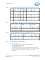
Single-Channel Mode
In this mode, all memory cycles are directed to a single-channel. Single-channel mode
is used when either Channel A or Channel B are populated in any order, but not both.
Dual-Channel Mode – Intel® Flex Memory Technology Mode
The system memory controller supports Intel Flex Memory Technology Mode where
memory is divided into a symmetric and asymmetric zone. The symmetric zone starts
at the lowest address in each channel and is contiguous until the asymmetric zone
begins or until the top address of the channel with the smaller capacity is reached. In
this mode, the system runs with one zone of dual-channel mode and one zone of
single-channel mode, simultaneously, across the entire memory array. This mode is
used when both Channel A and Channel B are populated with memory but the total
amount of memory in each channel is not the same.
Note:
Channels A and B can be mapped for Physical Channel 0 and 1 respectively or vice
versa; however, the Channel A size must be greater or equal to the Channel B size.
5th Generation Intel® Core™ Processor Family, Intel® Core™ M Processor Family, Mobile Intel® Pentium® Processor Family, and
Mobile Intel® Celeron® Processor Family
March 2015
Datasheet – Volume 1 of 2
Order No.: 330834-004v1
21
Processor—Interfaces
Figure 2.
Intel® Flex Memory Technology Operations
TOM
C
Non interleaved
access
B
C
B
B
CH A
CH B
Dual channel
interleaved access
B
CH A and CH B can be configured to be physical channels 0 or 1
B – The largest physical memory amount of the smaller size memory module
C – The remaining physical memory amount of the larger size memory module
Dual-Channel Symmetric Mode
Dual-Channel Symmetric mode, also known as interleaved mode, provides maximum
performance on real world applications. Addresses are ping-ponged between the
channels after each cache line (64-byte boundary). If there are two requests, and the
second request is to an address on the opposite channel from the first, that request
can be sent before data from the first request has returned. If two consecutive cache
lines are requested, both may be retrieved simultaneously, since they are ensured to
be on opposite channels. This mode is used when both Channel A and Channel B are
populated with the same amount of total memory.
2.1.6
Data Scrambling
The system memory controller incorporates a Data Scrambling feature to minimize the
impact of excessive di/dt on the platform system memory VRs due to successive 1s
and 0s on the data bus. Past experience has demonstrated that traffic on the data bus
is not random and can have energy concentrated at specific spectral harmonics
creating high di/dt, which is generally limited by data patterns that excite resonance
between the package inductance and on die capacitances. As a result, the system
memory controller uses a data scrambling feature to create pseudo-random patterns
on the system memory data bus to reduce the impact of any excessive di/dt.
2.2
Processor Graphics
The processor graphics contains a generation 8 graphics core architecture. This
enables substantial gains in performance and lower power consumption over previous
generations.
5th Generation Intel® Core™ Processor Family, Intel® Core™ M Processor Family, Mobile Intel® Pentium® Processor Family, and
Mobile Intel® Celeron® Processor Family
Datasheet – Volume 1 of 2
March 2015
22
Order No.: 330834-004v1
Interfaces—Processor
•
•
Next Generation Intel Clear Video Technology HD Support is a collection of video
playback and enhancement features that improve the end user’s viewing
experience
—
Encode / transcode HD content
—
Playback of high definition content including Blu-ray Disc*
—
Superior image quality with sharper, more colorful images
—
Playback of Blu-ray* disc S3D content using HDMI (1.4a specification
compliant with 3D)
DirectX* Video Acceleration (DXVA) support for accelerating video processing
—
•
•
2.3
Full AVC/VC1/MPEG2 HW Decode
Scalable Video Codec (SVC) Decode/Encode HW Acceleration
—
Extension of H.264 format
—
Single video stream with multiple subset bit streams or enhancement layers
VP8* Decode HW Acceleration
—
Open Source Codec
—
Full HW Acceleration for decode support
•
Advanced Scheduler 2.0, 1.0, XPDM support
•
Wineows* 8.1, Windows* 8, Windows* 7, OSX, Linux* operating system support
•
DirectX* 11.1, DirectX* 11.1+, DirectX* 11, DirectX* 10.1, DirectX* 10, DirectX*
9 support.
•
OpenGL* 4.0, OpenGL* 4.2 support
Processor Graphics Controller (GT)
The Graphics Engine Architecture includes 3D compute elements, Multi-format HW
assisted decode/encode pipeline, and Mid-Level Cache (MLC) for superior high
definition playback, video quality, and improved 3D performance and media.
The Display Engine handles delivering the pixels to the screen. GSA (Graphics in
System Agent) is the primary channel interface for display memory accesses and
“PCI-like” traffic in and out.
2.3.1
3D and Video Engines for Graphics Processing
The Gen 8 3D engine provides the following performance and power-management
enhancements.
3D Pipeline
The 3D graphics pipeline architecture simultaneously operates on different primitives
or on different portions of the same primitive. All the cores are fully programmable,
increasing the versatility of the 3D Engine.
3D Engine Execution Units
•
The EUs perform 128-bit wide execution per clock.
•
Support SIMD8 instructions for vertex processing and SIMD16 instructions for
pixel processing.
5th Generation Intel® Core™ Processor Family, Intel® Core™ M Processor Family, Mobile Intel® Pentium® Processor Family, and
Mobile Intel® Celeron® Processor Family
March 2015
Datasheet – Volume 1 of 2
Order No.: 330834-004v1
23
Processor—Interfaces
Vertex Fetch (VF) Stage
The VF stage executes 3DPRIMITIVE commands. Some enhancements have been
included to better support legacy D3D APIs as well as SGI OpenGL*.
Vertex Shader (VS) Stage
The VS stage performs shading of vertices output by the VF function. The VS unit
produces an output vertex reference for every input vertex reference received from
the VF unit, in the order received.
Geometry Shader (GS) Stage
The GS stage receives inputs from the VS stage. Compiled application-provided GS
programs, specifying an algorithm to convert the vertices of an input object into some
output primitives. For example, a GS shader may convert lines of a line strip into
polygons representing a corresponding segment of a blade of grass centered on the
line. Or it could use adjacency information to detect silhouette edges of triangles and
output polygons extruding out from the edges.
Clip Stage
The Clip stage performs general processing on incoming 3D objects. However, it also
includes specialized logic to perform a Clip Test function on incoming objects. The Clip
Test optimizes generalized 3D Clipping. The Clip unit examines the position of
incoming vertices, and accepts/rejects 3D objects based on its Clip algorithm.
Strips and Fans (SF) Stage
The SF stage performs setup operations required to rasterize 3D objects. The outputs
from the SF stage to the Windower stage contain implementation-specific information
required for the rasterization of objects and also supports clipping of primitives to
some extent.
Windower / IZ (WIZ) Stage
The WIZ unit performs an early depth test, which removes failing pixels and
eliminates unnecessary processing overhead.
The Windower uses the parameters provided by the SF unit in the object-specific
rasterization algorithms. The WIZ unit rasterizes objects into the corresponding set of
pixels. The Windower is also capable of performing dithering, whereby the illusion of a
higher resolution when using low-bpp channels in color buffers is possible. Color
dithering diffuses the sharp color bands seen on smooth-shaded objects.
Video Engine
The Video Engine handles the non-3D (media/video) applications. It includes support
for VLD and MPEG2 decode in hardware.
2D Engine
The 2D Engine contains BLT (Block Level Transfer) functionality and an extensive set
of 2D instructions. To take advantage of the 3D during engine’s functionality, some
BLT functions make use of the 3D renderer.
5th Generation Intel® Core™ Processor Family, Intel® Core™ M Processor Family, Mobile Intel® Pentium® Processor Family, and
Mobile Intel® Celeron® Processor Family
Datasheet – Volume 1 of 2
March 2015
24
Order No.: 330834-004v1
Interfaces—Processor
Logical 128-Bit Fixed BLT and 256 Fill Engine
This BLT engine accelerates the GUI of Microsoft Windows* operating systems. The
128-bit BLT engine provides hardware acceleration of block transfers of pixel data for
many common Windows operations. The BLT engine can be used for the following:
•
Move rectangular blocks of data between memory locations
•
Data alignment
•
To perform logical operations (raster ops)
The rectangular block of data does not change, as it is transferred between memory
locations. The allowable memory transfers are between: cacheable system memory
and frame buffer memory, frame buffer memory and frame buffer memory, and within
system memory. Data to be transferred can consist of regions of memory, patterns, or
solid color fills. A pattern is always 8 x 8 pixels wide and may be 8, 16, or 32 bits per
pixel.
The BLT engine expands monochrome data into a color depth of 8, 16, or 32 bits.
BLTs can be either opaque or transparent. Opaque transfers move the data specified
to the destination. Transparent transfers compare destination color to source color and
write according to the mode of transparency selected.
Data is horizontally and vertically aligned at the destination. If the destination for the
BLT overlaps with the source memory location, the BLT engine specifies which area in
memory to begin the BLT transfer. Hardware is included for all 256 raster operations
(source, pattern, and destination) defined by Microsoft*, including transparent BLT.
The BLT engine has instructions to invoke BLT and stretch BLT operations, permitting
software to set up instruction buffers and use batch processing. The BLT engine can
perform hardware clipping during BLTs.
2.4
Digital Display Interface (DDI)
•
The processor supports:
—
Two Digital Display (x4 DDI) interfaces that can be configured as DisplayPort*,
HDMI*. The DisplayPort* can be configured to use 1, 2, or 4 lanes depending
on the bandwidth requirements and link data rate of RBR (1.62 GT/s), HBR
(2.97 GT/s), and HBR2 (5.4 GT/s). When configured as HDMI*, the DDIx4
port can support 2.97 GT/s.
—
One dedicated x4 embedded DisplayPort* (eDP*). Built-in displays are only
supported on eDP.
•
The HDMI* interface supports HDMI with 3D, 4K, Deep Color, and x.v.Color. The
DisplayPort* interface supports the VESA DisplayPort* Standard Version 1,
Revision 2.
•
The processor supports High-bandwidth Digital Content Protection (HDCP) for
high-definition content playback over digital interfaces.
•
The processor also integrates dedicated a Mini HD audio controller to drive audio
on integrated digital display interfaces, such as HDMI* and DisplayPort*. The HD
audio controller on the PCH would continue to support down CODECs, and so on.
The processor Mini HD audio controller supports two High-Definition Audio streams
simultaneously on any of the three digital ports.
5th Generation Intel® Core™ Processor Family, Intel® Core™ M Processor Family, Mobile Intel® Pentium® Processor Family, and
Mobile Intel® Celeron® Processor Family
March 2015
Datasheet – Volume 1 of 2
Order No.: 330834-004v1
25
Processor—Interfaces
The processor supports streaming any 3 independent and simultaneous display
combination of DisplayPort*/HDMI*/eDP*/ monitors. In the case of 3
simultaneous displays, two High Definition Audio streams over the digital display
interfaces are supported.
•
Each digital port is capable of driving resolutions up to 3840x2160 at 60 Hz using
4 lanes at link data rate HBR2 through DisplayPort* and 4096x2304 at 24 Hz
using HDMI*. Use of active level shifter is required to obtain maximum HDMI
resolution.
•
DisplayPort* Aux CH, DDC channel, Panel power sequencing, and HPD are
supported through the PCH.
Processor Display Architecture
eDP* Mux
X4 eDP
eDP
Transcoder C
DP / HDMI
Timing, VDIP
HD Audio
Controller
X4 DP /
HDMI
X4 DP /
HDMI
PCH Display Control Signals
Display
Pipe C
Transcoder B
DP / HDMI
Timing, VDIP
DDI Ports B and C
Display
Pipe B
DP
Aux
Transcoder A
DP / HDMI
Timing, VDIP
Panel Fitting
Memory \ Config Interface
Display
Pipe A
Transcoder eDP*
DP encoder
Timing, VDIP
DPT, SRID
Port Mux
Figure 3.
•
Audio
Codec
Display is the presentation stage of graphics. This involves:
•
Pulling rendered data from memory
•
Converting raw data into pixels
•
Blending surfaces into a frame
•
Organizing pixels into frames
•
Optionally scaling the image to the desired size
•
Re-timing data for the intended target
•
Formatting data according to the port output standard
DisplayPort*
DisplayPort* is a digital communication interface that uses differential signaling to
achieve a high-bandwidth bus interface designed to support connections between PCs
and monitors, projectors, and TV displays.
5th Generation Intel® Core™ Processor Family, Intel® Core™ M Processor Family, Mobile Intel® Pentium® Processor Family, and
Mobile Intel® Celeron® Processor Family
Datasheet – Volume 1 of 2
March 2015
26
Order No.: 330834-004v1
Interfaces—Processor
A DisplayPort* consists of a Main Link, Auxiliary channel, and a Hot-Plug Detect signal.
The Main Link is a unidirectional, high-bandwidth, and low latency channel used for
transport of isochronous data streams such as uncompressed video and audio. The
Auxiliary Channel (AUX CH) is a half-duplex bidirectional channel used for link
management and device control. The Hot-Plug Detect (HPD) signal serves as an
interrupt request for the sink device.
The processor is designed in accordance with the VESA DisplayPort* Standard Version
1.2a. The processor supports VESA DisplayPort* PHY Compliance Test Specification
1.2a and VESA DisplayPort* Link Layer Compliance Test Specification 1.2a.
Figure 4.
DisplayPort* Overview
Source Device
DisplayPort Tx
Main Link
(Isochronous Streams)
Sink Device
DisplayPort Rx
AUX CH
(Link/Device Managemet)
Hot-Plug Detect
(Interrupt Request)
High-Definition Multimedia Interface (HDMI*)
The High-Definition Multimedia Interface* (HDMI*) is provided for transmitting
uncompressed digital audio and video signals from DVD players, set-top boxes, and
other audiovisual sources to television sets, projectors, and other video displays. It
can carry high quality multi-channel audio data and all standard and high-definition
consumer electronics video formats. The HDMI display interface connecting the
processor and display devices uses transition minimized differential signaling (TMDS)
to carry audiovisual information through the same HDMI cable.
HDMI includes three separate communications channels — TMDS, DDC, and the
optional CEC (consumer electronics control). CEC is not supported on the processor.
As shown in the following figure, the HDMI cable carries four differential pairs that
make up the TMDS data and clock channels. These channels are used to carry video,
audio, and auxiliary data. In addition, HDMI carries a VESA DDC. The DDC is used by
an HDMI Source to determine the capabilities and characteristics of the Sink.
Audio, video, and auxiliary (control/status) data is transmitted across the three TMDS
data channels. The video pixel clock is transmitted on the TMDS clock channel and is
used by the receiver for data recovery on the three data channels. The digital display
data signals driven natively through the PCH are AC coupled and needs level shifting
to convert the AC coupled signals to the HDMI compliant digital signals.
The processor HDMI interface is designed in accordance with the High-Definition
Multimedia Interface with 3D, 4K, Deep Color, and x.v.Color.
5th Generation Intel® Core™ Processor Family, Intel® Core™ M Processor Family, Mobile Intel® Pentium® Processor Family, and
Mobile Intel® Celeron® Processor Family
March 2015
Datasheet – Volume 1 of 2
Order No.: 330834-004v1
27
Processor—Interfaces
Figure 5.
HDMI* Overview
HDMI Sink
HDMI Source
HDMI Tx
HDMI Rx
TMDS Data Channel 0
TMDS Data Channel 1
TMDS Data Channel 2
TMDS Clock Channel
Hot-Plug Detect
Display Data Channel (DDC)
CEC Line (optional)
embedded DisplayPort*
The embedded DisplayPort* (eDP*) is an embedded version of the DisplayPort
standard oriented towards applications such as notebook and All-In-One PCs. Like
DisplayPort, embedded DisplayPort also consists of a Main Link, Auxiliary channel, and
an optional Hot-Plug Detect signal.
Integrated Audio
Table 8.
•
HDMI and display port interfaces carry audio along with video.
•
Processor supports two DMA controllers to output two High Definition audio
streams on two digital ports simultaneously.
•
Supports only the internal HDMI and DP CODECs.
Processor Supported Audio Formats over HDMI*and DisplayPort*
Audio Formats
HDMI*
DisplayPort*
AC-3 Dolby* Digital
Yes
Yes
Dolby Digital Plus
Yes
Yes
DTS-HD*
Yes
Yes
LPCM, 192 kHz/24 bit, 8 Channel
Yes
Yes
Dolby TrueHD, DTS-HD Master Audio*
(Lossless Blu-Ray Disc* Audio Format)
Yes
Yes
5th Generation Intel® Core™ Processor Family, Intel® Core™ M Processor Family, Mobile Intel® Pentium® Processor Family, and
Mobile Intel® Celeron® Processor Family
Datasheet – Volume 1 of 2
March 2015
28
Order No.: 330834-004v1
Interfaces—Processor
The processor will continue to support Silent stream. Silent stream is an integrated
audio feature that enables short audio streams, such as system events to be heard
over the HDMI and DisplayPort monitors. The processor supports silent streams over
the HDMI and DisplayPort interfaces at 44.1 kHz, 48 kHz, 88.2 kHz, 96 kHz,
176.4 kHz, and 192 kHz sampling rates.
Multiple Display Configurations
The following multiple display configuration modes are supported (with appropriate
driver software):
•
Single Display is a mode with one display port activated to display the output to
one display device. If the external port is activated, it should always use the
physical port B.
•
Intel Display Clone is a mode with up to three display ports activated to drive the
display content of same color depth setting but potentially different refresh rate
and resolution settings to all the active display devices connected.
•
Extended Desktop is a mode with up to three display ports activated to drive the
content with potentially different color depth, refresh rate, and resolution settings
on each of the active display devices connected.
The digital ports on the processor can be configured to support DisplayPort*/HDMI.
The following table shows examples of valid three display configurations through the
processor.
Table 9.
Multiple Display Configuration for 5th Generation Intel® Core™ Processor
Family, Mobile Intel® Pentium® Processor Family, and Mobile Intel® Celeron®
Processor Family
Display 1
Display 2
Display 3
Maximum
Resolution
Display 1
Maximum
Resolution
Display 2
Maximum
Resolution
Display 3
HDMI with
Active Level
Shifter
HDMI with
Active Level
Shifter
eDP
4096x2304 @ 24 Hz
3840x2160
@ 60 Hz
HDMI
HDMI
eDP
2560x1600 @ 60 Hz
3840x2160
@ 60 Hz
DP
DP
eDP
3840x2160 @ 60 Hz
3840x2160
@ 60 Hz
HDMI with
Active Level
Shifter
DP
eDP
4096x2304
@ 24 Hz
3840x2160
@ 60 Hz
3840x2160
@ 60 Hz
HDMI
DP
eDP
2560x1600
@ 60 Hz
3840x2160
@ 60 Hz
3840x2160
@ 60 Hz
Notes
Note: DP and eDP resolutions in this table are supported for 4 lanes with link data rate HBR2 at 24 bits per
pixel (bpp) and single stream mode of operation.
5th Generation Intel® Core™ Processor Family, Intel® Core™ M Processor Family, Mobile Intel® Pentium® Processor Family, and
Mobile Intel® Celeron® Processor Family
March 2015
Datasheet – Volume 1 of 2
Order No.: 330834-004v1
29
Processor—Interfaces
Table 10.
Multiple Display Configuration for Intel® Core™ M Processor Family
Display 1
Display 2
Display 3
HDMI with
Active Level
Shifter
HDMI with
Active Level
Shifter
eDP
HDMI
HDMI
DP
Maximum
Resolution
Display 1
Maximum
Resolution
Display 2
Maximum
Resolution
Display 3
Notes
4096x2304 @ 24 Hz
3200x2000
@ 60 Hz
Additional
100 mW
cooling
required
eDP
2560x1600 @ 60 Hz
3200x2000
@ 60 Hz
Additional
100 mW
cooling
required
DP
eDP
3200x2000 @ 60 Hz
3200x2000
@ 60 Hz
Additional
100 mW
cooling
required
HDMI with
Active Level
Shifter
DP
eDP
4096x2304
@ 24 Hz
3200x2000
@ 60 Hz
3200x2000
@ 60 Hz
Additional
100 mW
cooling
required
HDMI
DP
eDP
2560x1600
@ 60 Hz
3200x2000
@ 60 Hz
3200x2000
@ 60 Hz
Additional
100 mW
cooling
required
eDP
4096x2304
@ 24 Hz
2560x1600
@ 60 Hz
2560x1600
@ 60 Hz
Maximum
resolution for
clone or
duplicate
screen mode.
2560x1600
@ 60 Hz
2560x1600
@ 60 Hz
Maximum
resolution for
clone or
duplicate
screen mode.
3840x2160
@ 60 Hz
N/A
HDMI with
Active Level
Shifter
DP
HDMI
DP
eDP
2560x1600
@ 60 Hz
DP
eDP
N/A
2560x1600
@ 60 Hz
Additional
100 mW
cooling
required
Note: DP and eDP resolutions in this table are supported for 4 lanes with link data rate HBR2 at 24 bits per
pixel (bpp) and single stream mode of operation.
The following table shows the DisplayPort / embedded DisplayPort* resolutions
supported for 1, 2, or 4 lanes depending on link data rate of RBR, HBR, HBR2.
Table 11.
DisplayPort and embedded DisplayPort* Resolutions for 1, 2, 4 Lanes – Link
Data Rate of RBR, HBR, and HBR2 for U-Processor Line
Link Data Rate
Lane Count
1
2
4
RBR
1064x600
1400x1050
2240x1400
HBR
1280x960
1920x1200
2880x1800
HBR2
1920x1200
2880x1800
3840x2160
5th Generation Intel® Core™ Processor Family, Intel® Core™ M Processor Family, Mobile Intel® Pentium® Processor Family, and
Mobile Intel® Celeron® Processor Family
Datasheet – Volume 1 of 2
March 2015
30
Order No.: 330834-004v1
Interfaces—Processor
Table 12.
DisplayPort and embedded DisplayPort* Resolutions for 1, 2, 4 Lanes – Link
Data Rate of RBR, HBR, and HBR2 for Intel® Core™ M Processor Family
Link Data Rate
Lane Count
1
2
4
RBR
1064x600
1400x1050
2240x1400
HBR
1280x960
1920x1200
2560x1600
HBR2
1920x1200
2880x1800
3200x2000
High-bandwidth Digital Content Protection (HDCP)
HDCP is the technology for protecting high-definition content against unauthorized
copy or unreceptive between a source (computer, digital set top boxes, and so on)
and the sink (panels, monitor, and TVs). The processor supports HDCP 1.4 for content
protection over wired displays (HDMI* and DisplayPort*).
The HDCP 1.4 keys are integrated into the processor and customers are not required
to physically configure or handle the keys.
2.5
Platform Environmental Control Interface (PECI)
PECI is an Intel proprietary interface that provides a communication channel between
Intel processors and external components, like Super I/O (SIO) and Embedded
Controllers (EC), to provide processor temperature, Turbo, Configurable TDP, and
memory throttling control mechanisms and many other services. PECI is used for
platform thermal management and real time control and configuration of processor
features and performance.
2.5.1
PECI Bus Architecture
The PECI architecture is based on a wired-OR bus that the clients (as processor PECI)
can pull up high (with strong drive).
The idle state on the bus is near zero.
The following figure demonstrates PECI design and connectivity. While the host/
originator can be a third party PECI host, one of the PECI clients is a processor PECI
device.
5th Generation Intel® Core™ Processor Family, Intel® Core™ M Processor Family, Mobile Intel® Pentium® Processor Family, and
Mobile Intel® Celeron® Processor Family
March 2015
Datasheet – Volume 1 of 2
Order No.: 330834-004v1
31
Processor—Interfaces
Figure 6.
PECI Host-Clients Connection Example
VTT
VTT
Q3
nX
Q1
nX
PECI
Q2
1X
CPECI
<10pF/Node
Host / Originator
PECI Client
Additional
PECI Clients
5th Generation Intel® Core™ Processor Family, Intel® Core™ M Processor Family, Mobile Intel® Pentium® Processor Family, and
Mobile Intel® Celeron® Processor Family
Datasheet – Volume 1 of 2
March 2015
32
Order No.: 330834-004v1
Technologies—Processor
3.0
Technologies
This chapter provides a high-level description of Intel technologies implemented in the
processor.
The implementation of the features may vary between the processor SKUs.
Details on the different technologies of Intel processors and other relevant external
notes are located at the Intel technology web site: http://www.intel.com/technology/
3.1
Intel® Virtualization Technology (Intel® VT)
Intel® Virtualization Technology (Intel® VT) makes a single system appear as multiple
independent systems to software. This allows multiple, independent operating systems
to run simultaneously on a single system. Intel VT comprises technology components
to support virtualization of platforms based on Intel architecture microprocessors and
chipsets.
Intel® Virtualization Technology (Intel® VT) for IA-32, Intel® 64 and Intel®
Architecture (Intel® VT-x) added hardware support in the processor to improve the
virtualization performance and robustness. Intel® Virtualization Technology for
Directed I/O (Intel VT-d) extends Intel® VT-x by adding hardware assisted support to
improve I/O device virtualization performance.
Intel® VT-x specifications and functional descriptions are included in the Intel® 64 and
IA-32 Architectures Software Developer’s Manual, Volume 3B and is available at:
http://www.intel.com/products/processor/manuals/index.htm
The Intel VT-d specification and other Intel VT documents can be referenced at:
http://www.intel.com/technology/virtualization/index.htm
https://sharedspaces.intel.com/sites/PCDC/SitePages/Ingredients/ingredient.aspx?
ing=VT
Intel® VT-x Objectives
Intel VT-x provides hardware acceleration for virtualization of IA platforms. Virtual
Machine Monitor (VMM) can use Intel VT-x features to provide an improved reliable
virtualized platform. By using Intel VT-x, a VMM is:
•
Robust: VMMs no longer need to use paravirtualization or binary translation. This
means that off-the-shelf operating systems and applications can be run without
any special steps.
•
Enhanced: Intel VT enables VMMs to run 64-bit guest operating systems on IA
x86 processors.
5th Generation Intel® Core™ Processor Family, Intel® Core™ M Processor Family, Mobile Intel® Pentium® Processor Family, and
Mobile Intel® Celeron® Processor Family
March 2015
Datasheet – Volume 1 of 2
Order No.: 330834-004v1
33
Processor—Technologies
•
More reliable: Due to the hardware support, VMMs can now be smaller, less
complex, and more efficient. This improves reliability and availability and reduces
the potential for software conflicts.
•
More secure: The use of hardware transitions in the VMM strengthens the
isolation of VMs and further prevents corruption of one VM from affecting others
on the same system.
Intel® VT-x Features
The processor supports the following Intel VT-x features:
•
Extended Page Table (EPT) Accessed and Dirty Bits
—
•
Extended Page Table Pointer (EPTP) switching
—
•
EPT A/D bits enabled VMMs to efficiently implement memory management and
page classification algorithms to optimize VM memory operations, such as defragmentation, paging, live migration, and check-pointing. Without hardware
support for EPT A/D bits, VMMs may need to emulate A/D bits by marking EPT
paging-structures as not-present or read-only, and incur the overhead of EPT
page-fault VM exits and associated software processing.
EPTP switching is a specific VM function. EPTP switching allows guest software
(in VMX non-root operation, supported by EPT) to request a different EPT
paging-structure hierarchy. This is a feature by which software in VMX nonroot operation can request a change of EPTP without a VM exit. Software can
choose among a set of potential EPTP values determined in advance by
software in VMX root operation.
Pause loop exiting
—
Support VMM schedulers seeking to determine when a virtual processor of a
multiprocessor virtual machine is not performing useful work. This situation
may occur when not all virtual processors of the virtual machine are currently
scheduled and when the virtual processor in question is in a loop involving the
PAUSE instruction. The new feature allows detection of such loops and is thus
called PAUSE-loop exiting.
The processor core supports the following Intel VT-x features:
•
•
•
Extended Page Tables (EPT)
—
EPT is hardware assisted page table virtualization.
—
It eliminates VM exits from the guest operating system to the VMM for shadow
page-table maintenance.
Virtual Processor IDs (VPID)
—
Ability to assign a VM ID to tag processor core hardware structures (such as
TLBs).
—
This avoids flushes on VM transitions to give a lower-cost VM transition time
and an overall reduction in virtualization overhead.
Guest Preemption Timer
—
Mechanism for a VMM to preempt the execution of a guest operating system
after an amount of time specified by the VMM. The VMM sets a timer value
before entering a guest.
—
The feature aids VMM developers in flexibility and Quality of Service (QoS)
guarantees.
5th Generation Intel® Core™ Processor Family, Intel® Core™ M Processor Family, Mobile Intel® Pentium® Processor Family, and
Mobile Intel® Celeron® Processor Family
Datasheet – Volume 1 of 2
March 2015
34
Order No.: 330834-004v1
Technologies—Processor
•
Descriptor-Table Exiting
—
Descriptor-table exiting allows a VMM to protect a guest operating system
from an internal (malicious software based) attack by preventing relocation of
key system data structures like IDT (interrupt descriptor table), GDT (global
descriptor table), LDT (local descriptor table), and TSS (task segment
selector).
—
A VMM using this feature can intercept (by a VM exit) attempts to relocate
these data structures and prevent them from being tampered by malicious
software.
Intel® VT-d Objectives
The key Intel VT-d objectives are domain-based isolation and hardware-based
virtualization. A domain can be abstractly defined as an isolated environment in a
platform to which a subset of host physical memory is allocated. Intel VT-d provides
accelerated I/O performance for a virtualized platform and provides software with the
following capabilities:
•
I/O device assignment and security: for flexibly assigning I/O devices to VMs and
extending the protection and isolation properties of VMs for I/O operations.
•
DMA remapping: for supporting independent address translations for Direct
Memory Accesses (DMA) from devices.
•
Interrupt remapping: for supporting isolation and routing of interrupts from
devices and external interrupt controllers to appropriate VMs.
•
Reliability: for recording and reporting to system software DMA and interrupt
errors that may otherwise corrupt memory or impact VM isolation.
Intel VT-d accomplishes address translation by associating a transaction from a given
I/O device to a translation table associated with the Guest to which the device is
assigned. It does this by means of the data structure in the following illustration. This
table creates an association between the device's PCI Express* Bus/Device/Function
(B/D/F) number and the base address of a translation table. This data structure is
populated by a VMM to map devices to translation tables in accordance with the device
assignment restrictions above, and to include a multi-level translation table (VT-d
Table) that contains Guest specific address translations.
5th Generation Intel® Core™ Processor Family, Intel® Core™ M Processor Family, Mobile Intel® Pentium® Processor Family, and
Mobile Intel® Celeron® Processor Family
March 2015
Datasheet – Volume 1 of 2
Order No.: 330834-004v1
35
Processor—Technologies
Figure 7.
Device to Domain Mapping Structures
(Dev 31, Func 7)
Context entry 255
(Dev 0, Func 1)
(Dev 0, Func 0)
(Bus 255)
Root entry 255
(Bus N)
Root entry N
(Bus 0)
Root entry 0
Context entry 0
Context entry Table
For bus N
Address Translation
Structures for Domain A
Root entry table
Context entry 255
Context entry 0
Context entry Table
For bus 0
Address Translation
Structures for Domain B
Intel VT-d functionality, often referred to as an Intel VT-d Engine, has typically been
implemented at or near a PCI Express host bridge component of a computer system.
This might be in a chipset component or in the PCI Express functionality of a processor
with integrated I/O. When one such Intel VT-d engine receives a PCI Express
transaction from a PCI Express bus, it uses the B/D/F number associated with the
transaction to search for an Intel VT-d translation table. In doing so, it uses the B/D/F
number to traverse the data structure shown in the above figure. If it finds a valid
Intel VT-d table in this data structure, it uses that table to translate the address
provided on the PCI Express bus. If it does not find a valid translation table for a given
translation, this results in an Intel VT-d fault. If Intel VT-d translation is required, the
Intel VT-d engine performs an N-level table walk.
For more information, refer to Intel® Virtualization Technology for Directed I/O
Architecture Specification http://download.intel.com/technology/computing/vptech/
Intel(r)_VT_for_Direct_IO.pdf
Intel® VT-d Features
The processor supports the following Intel VT-d features:
5th Generation Intel® Core™ Processor Family, Intel® Core™ M Processor Family, Mobile Intel® Pentium® Processor Family, and
Mobile Intel® Celeron® Processor Family
Datasheet – Volume 1 of 2
March 2015
36
Order No.: 330834-004v1
Technologies—Processor
•
Memory controller and processor graphics comply with the Intel VT-d 1.2
Specification
•
Two Intel VT-d DMA remap engines
—
iGFX DMA remap engine
—
Default DMA remap engine (covers all devices except iGFX)
•
Support for root entry, context entry, and default context
•
39-bit guest physical address and host physical address widths
•
Support for 4 KB, 2 MB, and 1 GB page sizes
•
Support for register-based fault recording only (for single entry only) and support
for MSI interrupts for faults
•
Support for both leaf and non-leaf caching
•
Support for boot protection of default page table
•
Support for non-caching of invalid page table entries
•
Support for hardware-based flushing of translated but pending writes and pending
reads, on IOTLB invalidation
•
Support for Global, Domain specific, and Page specific IOTLB invalidation
•
MSI cycles (MemWr to address FEEx_xxxxh) not translated
—
Translation faults result in cycle forwarding to VBIOS region (byte enables
masked for writes). Returned data may be bogus for internal agents; PEG/DMI
interfaces return unsupported request status
•
Interrupt remapping is supported
•
Queued invalidation is supported
•
Intel VT-d translation bypass address range is supported (Pass Through)
The processor supports the following added new Intel VT-d features:
•
Intel VT-d superpage: support of Intel VT-d superpage (2 MB, 1 GB) for the
default Intel VT-d engine and Intel VT-D IGD engine (iGFX DMA remap engine
•
Support for LPSS device virtualization
Note:
Intel VT-d Technology may not be available on all SKUs.
3.2
Intel® Trusted Execution Technology (Intel® TXT)
Intel Trusted Execution Technology (Intel TXT) defines platform-level enhancements
that provide the building blocks for creating trusted platforms.
The Intel TXT platform helps to provide the authenticity of the controlling environment
such that those wishing to rely on the platform can make an appropriate trust
decision. The Intel TXT platform determines the identity of the controlling environment
by accurately measuring and verifying the controlling software.
Another aspect of the trust decision is the ability of the platform to resist attempts to
change the controlling environment. The Intel TXT platform will resist attempts by
software processes to change the controlling environment or bypass the bounds set by
the controlling environment.
5th Generation Intel® Core™ Processor Family, Intel® Core™ M Processor Family, Mobile Intel® Pentium® Processor Family, and
Mobile Intel® Celeron® Processor Family
March 2015
Datasheet – Volume 1 of 2
Order No.: 330834-004v1
37
Processor—Technologies
Intel TXT is a set of extensions designed to provide a measured and controlled launch
of system software that will then establish a protected environment for itself and any
additional software that it may execute.
These extensions enhance two areas:
•
The launching of the Measured Launched Environment (MLE).
•
The protection of the MLE from potential corruption.
The enhanced platform provides these launch and control interfaces using Safer Mode
Extensions (SMX).
The SMX interface includes the following functions:
•
Measured/Verified launch of the MLE.
•
Mechanisms to ensure the above measurement is protected and stored in a secure
location.
•
Protection mechanisms that allow the MLE to control attempts to modify itself.
The processor also offers additional enhancements to System Management Mode
(SMM) architecture for enhanced security and performance. The processor provides
new MSRs to:
•
Enable a second SMM range
•
Enable SMM code execution range checking
•
Select whether SMM Save State is to be written to legacy SMRAM or to MSRs
•
Determine if a thread is going to be delayed entering SMM
•
Determine if a thread is blocked from entering SMM
•
Targeted SMI, enable/disable threads from responding to SMIs both VLWs and IPI
For the above features, BIOS must test the associated capability bit before attempting
to access any of the above registers.
For more information, refer to the Intel® Trusted Execution Technology Measured
Launched Environment Programming Guide.
3.3
Intel® Hyper-Threading Technology (Intel® HT
Technology)
The processor supports Intel Hyper-Threading Technology (Intel HT Technology) that
allows an execution core to function as two logical processors. While some execution
resources, such as caches, execution units, and buses are shared, each logical
processor has its own architectural state with its own set of general-purpose registers
and control registers. This feature must be enabled using the BIOS and requires
operating system support.
Intel recommends enabling Intel HT Technology with Microsoft Windows* 8 ,
Windows* 8.1, and Microsoft Windows* 7 and disabling Intel HT Technology using the
BIOS for all previous versions of Windows* operating systems. For more information
on Intel HT Technology, see http://www.intel.com/technology/platform-technology/
hyper-threading/.
5th Generation Intel® Core™ Processor Family, Intel® Core™ M Processor Family, Mobile Intel® Pentium® Processor Family, and
Mobile Intel® Celeron® Processor Family
Datasheet – Volume 1 of 2
March 2015
38
Order No.: 330834-004v1
Technologies—Processor
3.4
Intel® Turbo Boost Technology 2.0
The Intel Turbo Boost Technology 2.0 allows the processor core to opportunistically
and automatically run faster than its rated operating frequency/render clock, if it is
operating below power, temperature, and current limits. The Intel Turbo Boost
Technology 2.0 feature is designed to increase performance of both multi-threaded
and single-threaded workloads.
Compared with previous generation products, Intel Turbo Boost Technology 2.0 will
increase the ratio of application power to TDP. Thus, thermal solutions and platform
cooling that are designed to less than thermal design guidance might experience
thermal and performance issues since more applications will tend to run at the
maximum power limit for significant periods of time.
Note:
Intel Turbo Boost Technology 2.0 may not be available on all SKUs.
Intel® Turbo Boost Technology 2.0 Frequency
To determine the highest performance frequency amongst active cores, the processor
takes the following into consideration:
•
The number of cores operating in the C0 state.
•
The estimated core current consumption.
•
The estimated package prior and present power consumption.
•
The package temperature.
Any of these factors can affect the maximum frequency for a given workload. If the
power, current, or thermal limit is reached, the processor will automatically reduce the
frequency to stay within its TDP limit. Turbo processor frequencies are only active if
the operating system is requesting the P0 state. For more information on P-states and
C-states, see Power Management on page 44.
3.5
Intel® Advanced Vector Extensions 2.0 (Intel® AVX2)
Intel Advanced Vector Extensions 2.0 (Intel AVX2) is the latest expansion of the Intel
instruction set. Intel AVX2 extends the Intel Advanced Vector Extensions (Intel AVX)
with 256-bit integer instructions, floating-point fused multiply add (FMA) instructions,
and gather operations. The 256-bit integer vectors benefit math, codec, image, and
digital signal processing software. FMA improves performance in face detection,
professional imaging, and high performance computing. Gather operations increase
vectorization opportunities for many applications. In addition to the vector extensions,
this generation of Intel processors adds new bit manipulation instructions useful in
compression, encryption, and general purpose software.
For more information on Intel AVX, see http://www.intel.com/software/avx
3.6
Intel® Advanced Encryption Standard New Instructions
(Intel® AES-NI)
The processor supports Intel Advanced Encryption Standard New Instructions (Intel
AES-NI) that are a set of Single Instruction Multiple Data (SIMD) instructions that
enable fast and secure data encryption and decryption based on the Advanced
Encryption Standard (AES). Intel AES-NI are valuable for a wide range of
5th Generation Intel® Core™ Processor Family, Intel® Core™ M Processor Family, Mobile Intel® Pentium® Processor Family, and
Mobile Intel® Celeron® Processor Family
March 2015
Datasheet – Volume 1 of 2
Order No.: 330834-004v1
39
Processor—Technologies
cryptographic applications, such as applications that perform bulk encryption/
decryption, authentication, random number generation, and authenticated encryption.
AES is broadly accepted as the standard for both government and industry
applications, and is widely deployed in various protocols.
Intel AES-NI consists of six Intel SSE instructions. Four instructions, AESENC,
AESENCLAST, AESDEC, and AESDELAST facilitate high performance AES encryption
and decryption. The other two, AESIMC and AESKEYGENASSIST, support the AES key
expansion procedure. Together, these instructions provide a full hardware for
supporting AES; offering security, high performance, and a great deal of flexibility.
PCLMULQDQ Instruction
The processor supports the carry-less multiplication instruction, PCLMULQDQ.
PCLMULQDQ is a Single Instruction Multiple Data (SIMD) instruction that computes the
128-bit carry-less multiplication of two, 64-bit operands without generating and
propagating carries. Carry-less multiplication is an essential processing component of
several cryptographic systems and standards. Hence, accelerating carry-less
multiplication can significantly contribute to achieving high speed secure computing
and communication.
Intel® Secure Key
The processor supports Intel® Secure Key (formerly known as Digital Random Number
Generator (DRNG)), a software visible random number generation mechanism
supported by a high quality entropy source. This capability is available to
programmers through the RDRAND instruction. The resultant random number
generation capability is designed to comply with existing industry standards in this
regard (ANSI X9.82 and NIST SP 800-90).
Some possible usages of the RDRAND instruction include cryptographic key generation
as used in a variety of applications, including communication, digital signatures,
secure storage, and so on.
The processor has a RDSEED instruction that enables system software and security
vendors who need to seed or reseed a software PRNG.
The RDSEED instruction will be a companion to the RDRAND instruction. RDSEED,
along with RDRAND, fills out Intel's standards compliant (such as NIST SP800-90 A, B,
and C) Hardware-based Random Number Generator portfolio.
3.7
Intel® 64 Architecture x2APIC
The x2APIC architecture extends the xAPIC architecture that provides key
mechanisms for interrupt delivery. This extension is primarily intended to increase
processor addressability.
Specifically, x2APIC:
•
Retains all key elements of compatibility to the xAPIC architecture:
—
Delivery modes
—
Interrupt and processor priorities
—
Interrupt sources
—
Interrupt destination types
5th Generation Intel® Core™ Processor Family, Intel® Core™ M Processor Family, Mobile Intel® Pentium® Processor Family, and
Mobile Intel® Celeron® Processor Family
Datasheet – Volume 1 of 2
March 2015
40
Order No.: 330834-004v1
Technologies—Processor
•
Provides extensions to scale processor addressability for both the logical and
physical destination modes
•
Adds new features to enhance performance of interrupt delivery
•
Reduces complexity of logical destination mode interrupt delivery on link based
architectures
The key enhancements provided by the x2APIC architecture over xAPIC are the
following:
•
•
•
Support for two modes of operation to provide backward compatibility and
extensibility for future platform innovations:
—
In xAPIC compatibility mode, APIC registers are accessed through memory
mapped interface to a 4K-Byte page, identical to the xAPIC architecture.
—
In x2APIC mode, APIC registers are accessed through Model Specific Register
(MSR) interfaces. In this mode, the x2APIC architecture provides significantly
increased processor addressability and some enhancements on interrupt
delivery.
Increased range of processor addressability in x2APIC mode:
—
Physical xAPIC ID field increases from 8 bits to 32 bits, allowing for interrupt
processor addressability up to 4G–1 processors in physical destination mode.
A processor implementation of x2APIC architecture can support fewer than 32bits in a software transparent fashion.
—
Logical xAPIC ID field increases from 8 bits to 32 bits. The 32-bit logical
x2APIC ID is partitioned into two sub-fields – a 16-bit cluster ID and a 16-bit
logical ID within the cluster. Consequently, ((2^20) – 16) processors can be
addressed in logical destination mode. Processor implementations can support
fewer than 16 bits in the cluster ID sub-field and logical ID sub-field in a
software agnostic fashion.
More efficient MSR interface to access APIC registers:
—
Note:
To enhance inter-processor and self-directed interrupt delivery as well as the
ability to virtualize the local APIC, the APIC register set can be accessed only
through MSR-based interfaces in x2APIC mode. The Memory Mapped IO
(MMIO) interface used by xAPIC is not supported in x2APIC mode.
•
The semantics for accessing APIC registers have been revised to simplify the
programming of frequently-used APIC registers by system software. Specifically,
the software semantics for using the Interrupt Command Register (ICR) and End
Of Interrupt (EOI) registers have been modified to allow for more efficient delivery
and dispatching of interrupts.
•
The x2APIC extensions are made available to system software by enabling the
local x2APIC unit in the “x2APIC” mode. To benefit from x2APIC capabilities, a
new operating system and a new BIOS are both needed, with special support for
x2APIC mode.
•
The x2APIC architecture provides backward compatibility to the xAPIC architecture
and forward extendible for future Intel platform innovations.
Intel x2APIC Technology may not be available on all SKUs.
For more information, see the Intel® 64 Architecture x2APIC Specification at http://
www.intel.com/products/processor/manuals/.
5th Generation Intel® Core™ Processor Family, Intel® Core™ M Processor Family, Mobile Intel® Pentium® Processor Family, and
Mobile Intel® Celeron® Processor Family
March 2015
Datasheet – Volume 1 of 2
Order No.: 330834-004v1
41
Processor—Technologies
3.8
Power Aware Interrupt Routing (PAIR)
The processor includes enhanced power-performance technology that routes
interrupts to threads or cores based on their sleep states. As an example, for energy
savings, it routes the interrupt to the active cores without waking the deep idle cores.
For performance, it routes the interrupt to the idle (C1) cores without interrupting the
already heavily loaded cores. This enhancement is mostly beneficial for high-interrupt
scenarios like Gigabit LAN, WLAN peripherals, and so on.
3.9
Execute Disable Bit
The Execute Disable Bit allows memory to be marked as executable when combined
with a supporting operating system. If code attempts to run in non-executable
memory, the processor raises an error to the operating system. This feature can
prevent some classes of viruses or worms that exploit buffer overrun vulnerabilities
and can thus help improve the overall security of the system. See the Intel® 64 and
IA-32 Architectures Software Developer's Manuals for more detailed information.
3.10
Intel® Device Protection with Boot Guard
Intel® Device Protection with Boot Guard can help protect the platform boot integrity
by preventing execution of unauthorized boot blocks. With Intel® Device Protection
with Boot Guard, platform manufacturers can create boot policies such that invocation
of an unauthorized (or untrusted) boot block will trigger the platform protection per
the manufacturer's defined policy.
With verification based in the hardware, Intel® Device Protection with Boot Guard
extends the trust boundary of the platform boot process down to the hardware level.
Intel® Device Protection with Boot Guard accomplishes this by:
•
Providing hardware-based Static Root of Trust for Measurement (S-RTM) and the
Root of Trust for Verification (RTV) using Intel architectural components.
•
Providing architectural definition for platform manufacturer Boot Policy.
•
Enforcing manufacture provided Boot Policy using Intel architectural components.
Benefits of this protection is that Intel® Device Protection with Boot Guard can help
maintain platform integrity by preventing re-purposing of the manufacturer’s
hardware to run an unauthorized software stack.
Note:
Intel® Device Protection with Boot Guard technology availability may vary between
the different SKUs.
3.11
Supervisor Mode Execution Protection (SMEP)
Supervisor Mode Execution Protection provides the next level of system protection by
blocking malicious software attacks from user mode code when the system is running
in the highest privilege level. This technology helps to protect from virus attacks and
unwanted code from harming the system. For more information, refer to Intel® 64
and IA-32 Architectures Software Developer's Manual, Volume 3A at: http://
www.intel.com/Assets/PDF/manual/253668.pdf
5th Generation Intel® Core™ Processor Family, Intel® Core™ M Processor Family, Mobile Intel® Pentium® Processor Family, and
Mobile Intel® Celeron® Processor Family
Datasheet – Volume 1 of 2
March 2015
42
Order No.: 330834-004v1
Technologies—Processor
3.12
Supervisor Mode Access Protection (SMAP)
Supervisor Mode Access Protection provides the next level of system protection by
blocking a malicious user from tricking the operating system into branching off user
data. This technology shuts down very popular attack vectors against operating
systems . For more information, refer to the Intel® 64 and IA-32 Architectures
Software Developer's Manual, Volume 3A.
3.13
Intel® Transactional Synchronization Extensions - New
Instructions (Intel® TSX-NI)
The processor supports Intel Transactional Synchronization Extensions - New
Instructions (Intel TSX-NI). Intel TSX-NI provides a set of instruction extensions that
allow programmers to specify regions of code for transactional synchronization.
Programmers can use these extensions to achieve the performance of fine-grain
locking while actually programming using coarse-grain locks. Details on Intel TSX-NI
are in the Intel® Architecture Instruction Set Extensions Programming Reference.
5th Generation Intel® Core™ Processor Family, Intel® Core™ M Processor Family, Mobile Intel® Pentium® Processor Family, and
Mobile Intel® Celeron® Processor Family
March 2015
Datasheet – Volume 1 of 2
Order No.: 330834-004v1
43
Processor—Power Management
4.0
Power Management
This chapter provides information on the following power management topics:
Figure 8.
•
Advanced Configuration and Power Interface (ACPI) States
•
Processor Core
•
Integrated Memory Controller (IMC)
•
Processor Graphics Controller
Processor Power States
G0 – Working
S0 – Processor powered on (full on mode / connected standby mode)
C0 – Active mode
P0
Pn
C1 – Auto halt
C1E – Auto halt, low freq, low voltage
C3 – L1/L2 caches flush, clocks off
C6 – save core states before shutdown and PLL off
C7 – C6 + L3 cache flush
C8 – C7 internal voltage removal from all power domains
C9 – C8+VCC input to 0V
C10 – C9+VR12.6 shut off or PS4
G1 – Sleeping
S3 cold – Sleep – Suspend To Ram (STR)
S4 – Hibernate – Suspend To Disk (STD), Wakeup on PCH
G2 – Soft Off
S5 – Soft Off – no power,Wakeup on PCH
G3 – Mechanical Off
* Note: Power states availability may vary between the different SKUs
5th Generation Intel® Core™ Processor Family, Intel® Core™ M Processor Family, Mobile Intel® Pentium® Processor Family, and
Mobile Intel® Celeron® Processor Family
Datasheet – Volume 1 of 2
March 2015
44
Order No.: 330834-004v1
Power Management—Processor
Figure 9.
Processor Package and Core C-States
C0
C3
C6
C7
C8
C9
C10
One or more cores or GT executing instructions
All cores and GT in C3 or deeper, L3 may be flushed and turned off, memory in self refresh, some Uncore
clocks stopped, some Uncore voltages reduced
All cores and GT in C6 or deeper, L3 may be flushed and turned off, memory in self refresh, all Uncore
clocks stopped, some Uncore voltages reduced
Package C6 + L3 flushed and turned off, additional Uncore voltages reduced
Package C7 + most Uncore voltages reduced to 0V
Package C8 + VR12.6 in low power state
Package C9 + VR12.6 turned off
{
PACKAGE STATE
CORE STATE
C0 C1 C1E C3 C6 C7 C8 C9 C10
Core behaves the same as Core C6 state
All core clocks are stopped, core state saved and voltage reduce to 0V
Cores flush L1/L2 into L3, all core clocks are stopped
Core halted, most core clocks stopped and voltage reduced to Pn
Core halted, most core clocks stopped
Core is executing code
Possible combination of core/package states
Impossible combination of core/package states
Note: The “core state” relates to the core which is in the HIGHEST power state in the package (most active)
4.1
Advanced Configuration and Power Interface (ACPI)
States Supported
This section describes the ACPI states supported by the processor.
Table 13.
System States
State
G0/S0
Full On Mode, Display On.
G0/S0
Connected Standby Mode, Display Off.
G1/S3-Cold
Suspend-to-RAM (STR). Context saved to memory (S3-Hot state is not supported by the
processor).
G1/S4
Suspend-to-Disk (STD). All power lost (except wakeup on PCH).
G2/S5
Soft off. All power lost (except wakeup on PCH). Total reboot.
G3
Table 14.
Description
Mechanical off. All power removed from system.
Processor Core / Package State Support
State
Description
C0
Active mode, processor executing code.
C1
AutoHALT state.
C1E
AutoHALT state with lowest frequency and voltage operating point.
C3
Execution cores in C3 state flush their L1 instruction cache, L1 data cache, and L2 cache
to the L3 shared cache. Clocks are shut off to each core.
C6
Execution cores in this state save their architectural state before removing core voltage.
continued...
5th Generation Intel® Core™ Processor Family, Intel® Core™ M Processor Family, Mobile Intel® Pentium® Processor Family, and
Mobile Intel® Celeron® Processor Family
March 2015
Datasheet – Volume 1 of 2
Order No.: 330834-004v1
45
Processor—Power Management
State
Description
C7
Execution cores in this state behave similarly to the C6 state. If all execution cores
request C7 state, L3 cache ways are flushed until it is cleared. If the entire L3 cache is
flushed, voltage will be removed from the L3 cache. Power removal to SA, Cores and L3
will reduce power consumption.
C8
C7 state plus voltage is removed from all power domains after required state is saved. PLL
is powered down.
C9
C8 state plus processor VCC input voltage at 0 V.
C10
Table 15.
C9 state plus VR12.6 is set to low-power state, near shut off.
Integrated Memory Controller States
State
Description
Power up
CKE asserted. Active mode.
Pre-charge
Power-down
CKE de-asserted (not self-refresh) with all banks closed.
Active Powerdown
Self-Refresh
Table 16.
4.2
CKE de-asserted (not self-refresh) with minimum one bank active.
CKE de-asserted using device self-refresh.
G, S, and C Interface State Combinations
Global
(G)
State
Sleep (S)
State
Processor
Package (C)
State
Processor
State
System Clocks
Description
G0
S0
C0
Full On
On
Full On
G0
S0
C1/C1E
Auto-Halt
On
Auto-Halt
G0
S0
C3
Deep Sleep
On
Deep Sleep
G0
S0
C6/C7
Deep Powerdown
On
Deep Power-down
G0
S0
C8/C9/C10
On
Deeper Powerdown
G1
S3
Power off
Off, except RTC
Suspend to RAM
G1
S4
Power off
Off, except RTC
Suspend to Disk
G2
S5
Power off
Off, except RTC
Soft Off
G3
NA
Power off
Power off
Hard off
Processor Core Power Management
®
While executing code, Enhanced Intel SpeedStep Technology optimizes the
processor’s frequency and core voltage based on workload. Each frequency and
voltage operating point is defined by ACPI as a P-state. When the processor is not
executing code, it is idle. A low-power idle state is defined by ACPI as a C-state. In
general, deeper power C-states have longer entry and exit latencies.
4.2.1
Enhanced Intel® SpeedStep® Technology Key Features
The following are the key features of Enhanced Intel SpeedStep Technology:
5th Generation Intel® Core™ Processor Family, Intel® Core™ M Processor Family, Mobile Intel® Pentium® Processor Family, and
Mobile Intel® Celeron® Processor Family
Datasheet – Volume 1 of 2
March 2015
46
Order No.: 330834-004v1
Power Management—Processor
4.2.2
•
Multiple frequency and voltage points for optimal performance and power
efficiency. These operating points are known as P-states.
•
Frequency selection is software controlled by writing to processor MSRs. The
voltage is optimized based on the selected frequency and the number of active
processor cores.
—
Once the voltage is established, the PLL locks on to the target frequency.
—
All active processor cores share the same frequency and voltage. In a multicore processor, the highest frequency P-state requested among all active
cores is selected.
—
Software-requested transitions are accepted at any time. If a previous
transition is in progress, the new transition is deferred until the previous
transition is completed.
•
The processor controls voltage ramp rates internally to ensure glitch-free
transitions.
•
Because there is low transition latency between P-states, a significant number of
transitions per-second are possible.
Low-Power Idle States
When the processor is idle, low-power idle states (C-states) are used to save power.
More power savings actions are taken for numerically higher C-states. However,
higher C-states have longer exit and entry latencies. Resolution of C-states occur at
the thread, processor core, and processor package level. Thread-level C-states are
available if Intel Hyper-Threading Technology is enabled.
Caution:
Long term reliability cannot be assured unless all the Low-Power Idle States are
enabled.
Figure 10.
Idle Power Management Breakdown of the Processor Cores
Thread 0
Thread 1
Thread 0
Core 0 State
Thread 1
Core N State
Processor Package State
5th Generation Intel® Core™ Processor Family, Intel® Core™ M Processor Family, Mobile Intel® Pentium® Processor Family, and
Mobile Intel® Celeron® Processor Family
March 2015
Datasheet – Volume 1 of 2
Order No.: 330834-004v1
47
Processor—Power Management
While individual threads can request low-power C-states, power saving actions only
take place once the core C-state is resolved. Core C-states are automatically resolved
by the processor. For thread and core C-states, a transition to and from C0 is required
before entering any other C-state.
4.2.3
Requesting Low-Power Idle States
The primary software interfaces for requesting low-power idle states are through the
MWAIT instruction with sub-state hints and the HLT instruction (for C1 and C1E).
However, software may make C-state requests using the legacy method of I/O reads
from the ACPI-defined processor clock control registers, referred to as P_LVLx. This
method of requesting C-states provides legacy support for operating systems that
initiate C-state transitions using I/O reads.
For legacy operating systems, P_LVLx I/O reads are converted within the processor to
the equivalent MWAIT C-state request. Therefore, P_LVLx reads do not directly result
in I/O reads to the system. The feature, known as I/O MWAIT redirection, must be
enabled in the BIOS.
The BIOS can write to the C-state range field of the PMG_IO_CAPTURE MSR to restrict
the range of I/O addresses that are trapped and emulate MWAIT like functionality.
Any P_LVLx reads outside of this range do not cause an I/O redirection to MWAIT(Cx)
like request. The reads fall through like a normal I/O instruction.
Note:
When P_LVLx I/O instructions are used, MWAIT sub-states cannot be defined. The
MWAIT sub-state is always zero if I/O MWAIT redirection is used. By default, P_LVLx
I/O redirections enable the MWAIT 'break on EFLAGS.IF’ feature that triggers a
wakeup on an interrupt, even if interrupts are masked by EFLAGS.IF.
4.2.4
Core C-State Rules
The following are general rules for all core C-states, unless specified otherwise:
•
A core C-state is determined by the lowest numerical thread state (such as Thread
0 requests C1E state while Thread 1 requests C3 state, resulting in a core C1E
state). See the G, S, and C Interface State Combinations table.
•
A core transitions to C0 state when:
—
An interrupt occurs
—
There is an access to the monitored address if the state was entered using an
MWAIT/Timed MWAIT instruction
—
The deadline corresponding to the Timed MWAIT instruction expires
•
An interrupt directed toward a single thread wakes only that thread.
•
If any thread in a core is in active (in C0 state), the core's C-state will resolve to
C0 state.
•
Any interrupt coming into the processor package may wake any core.
•
A system reset re-initializes all processor cores.
Core C0 State
The normal operating state of a core where code is being executed.
5th Generation Intel® Core™ Processor Family, Intel® Core™ M Processor Family, Mobile Intel® Pentium® Processor Family, and
Mobile Intel® Celeron® Processor Family
Datasheet – Volume 1 of 2
March 2015
48
Order No.: 330834-004v1
Power Management—Processor
Core C1/C1E State
C1/C1E is a low power state entered when all threads within a core execute a HLT or
MWAIT(C1/C1E) instruction.
A System Management Interrupt (SMI) handler returns execution to either Normal
state or the C1/C1E state. See the Intel® 64 and IA-32 Architectures Software
Developer’s Manual for more information.
While a core is in C1/C1E state, it processes bus snoops and snoops from other
threads. For more information on C1E state, see Package C-States on page 50.
Core C3 State
Individual threads of a core can enter the C3 state by initiating a P_LVL2 I/O read to
the P_BLK or an MWAIT(C3) instruction. A core in C3 state flushes the contents of its
L1 instruction cache, L1 data cache, and L2 cache to the shared L3 cache, while
maintaining its architectural state. All core clocks are stopped at this point. Because
the core’s caches are flushed, the processor does not wake any core that is in the C3
state when either a snoop is detected or when another core accesses cacheable
memory.
Core C6 State
Individual threads of a core can enter the C6 state by initiating a P_LVL3 I/O read or
an MWAIT(C6) instruction. Before entering core C6 state, the core will save its
architectural state to a dedicated SRAM. Once complete, a core will have its voltage
reduced to zero volts. During exit, the core is powered on and its architectural state is
restored.
Core C7-C10 States
Individual threads of a core can enter the C7, C8, C9, or C10 state by initiating a
P_LVL4, P_LVL5, P_LVL6, P_LVL7 I/O read (respectively) to the P_BLK or by an
MWAIT(C7/C8/C9/C10) instruction. The core C7–C10 state exhibits the same behavior
as the core C6 state.
C-State Auto-Demotion
In general, deeper C-states, such as C6 or C7 state, have long latencies and have
higher energy entry/exit costs. The resulting performance and energy penalties
become significant when the entry/exit frequency of a deeper C-state is high.
Therefore, incorrect or inefficient usage of deeper C-states have a negative impact on
battery life and idle power. To increase residency and improve battery life and idle
power in deeper C-states, the processor supports C-state auto-demotion.
There are two C-state auto-demotion options:
•
C7/C6 to C3 state
•
C7/C6/C3 To C1 state
The decision to demote a core from C6/C7 to C3 or C3/C6/C7 to C1 state is based on
each core’s immediate residency history and interrupt rate . If the interrupt rate
experienced on a core is high and the residence in a deep C-state between such
interrupts is low, the core can be demoted to a C3 or C1 state. A higher interrupt
pattern is required to demote a core to C1 state as compared to C3 state.
5th Generation Intel® Core™ Processor Family, Intel® Core™ M Processor Family, Mobile Intel® Pentium® Processor Family, and
Mobile Intel® Celeron® Processor Family
March 2015
Datasheet – Volume 1 of 2
Order No.: 330834-004v1
49
Processor—Power Management
This feature is disabled by default. BIOS must enable it in the
PMG_CST_CONFIG_CONTROL register. The auto-demotion policy is also configured by
this register.
4.2.5
Package C-States
The processor supports C0, C1/C1E, C3, C6, C7, C8, C9, and C10 power states.The
following is a summary of the general rules for package C-state entry. These apply to
all package C-states, unless specified otherwise:
•
A package C-state request is determined by the lowest numerical core C-state
amongst all cores.
•
A package C-state is automatically resolved by the processor depending on the
core idle power states and the status of the platform components.
—
Each core can be at a lower idle power state than the package if the platform
does not grant the processor permission to enter a requested package C-state.
—
The platform may allow additional power savings to be realized in the
processor.
—
For package C-states, the processor is not required to enter C0 state before
entering any other C-state.
—
Entry into a package C-state may be subject to auto-demotion – that is, the
processor may keep the package in a deeper package C-state than requested
by the operating system if the processor determines, using heuristics, that the
deeper C-state results in better power/performance.
The processor exits a package C-state when a break event is detected. Depending on
the type of break event, the processor does the following:
•
•
If a core break event is received, the target core is activated and the break event
message is forwarded to the target core.
—
If the break event is not masked, the target core enters the core C0 state and
the processor enters package C0 state.
—
If the break event is masked, the processor attempts to re-enter its previous
package state.
If the break event was due to a memory access or snoop request,
—
But the platform did not request to keep the processor in a higher package Cstate, the package returns to its previous C-state.
—
And the platform requests a higher power C-state, the memory access or
snoop request is serviced and the package remains in the higher power Cstate.
The following table shows package C-state resolution for a dual-core processor. The
following figure summarizes package C-state transitions.
5th Generation Intel® Core™ Processor Family, Intel® Core™ M Processor Family, Mobile Intel® Pentium® Processor Family, and
Mobile Intel® Celeron® Processor Family
Datasheet – Volume 1 of 2
March 2015
50
Order No.: 330834-004v1
Power Management—Processor
Table 17.
Coordination of Core Power States at the Package Level
Package C-State
Core 0
Core 1
C0
C1
C3
C6
C7
C8
C9
C10
C0
C0
C0
C0
C0
C0
C0
C0
C0
C1
C0
C11
C11
C11
C11
C11
C11
C11
C3
C0
C11
C3
C3
C3
C3
C3
C3
C6
C0
C11
C3
C6
C6
C6
C6
C6
C7
C0
C11
C3
C6
C7
C7
C7
C7
C8
C0
C11
C3
C6
C7
C8
C8
C8
C9
C0
C11
C3
C6
C7
C8
C9
C9
C10
C0
C11
C3
C6
C7
C8
C9
C10
Note: 1. If enabled, the package C-state will be C1E if all cores have resolved a core C1 state or higher.
Figure 11.
Package C-State Entry and Exit
Package C0
Package C1/C1E
Package C3
Package C6
Package C7
Package C8
Package C9
Package C10
Package C0 State
This is the normal operating state for the processor. The processor remains in the
normal state when at least one of its cores is in the C0 or C1 state or when the
platform has not granted permission to the processor to go into a low-power state.
Individual cores may be in lower power idle states while the package is in C0 state.
Package C1/C1E State
No additional power reduction actions are taken in the package C1 state. However, if
the C1E sub-state is enabled, the processor automatically transitions to the lowest
supported core clock frequency, followed by a reduction in voltage.
The package enters the C1 low-power state when:
•
At least one core is in the C1 state.
•
The other cores are in a C1 or deeper power state.
The package enters the C1E state when:
•
All cores have directly requested C1E using MWAIT(C1) with a C1E sub-state hint.
5th Generation Intel® Core™ Processor Family, Intel® Core™ M Processor Family, Mobile Intel® Pentium® Processor Family, and
Mobile Intel® Celeron® Processor Family
March 2015
Datasheet – Volume 1 of 2
Order No.: 330834-004v1
51
Processor—Power Management
•
All cores are in a power state deeper than C1/C1E state; however, the package
low-power state is limited to C1/C1E using the PMG_CST_CONFIG_CONTROL MSR.
•
All cores have requested C1 state using HLT or MWAIT(C1) and C1E autopromotion is enabled in IA32_MISC_ENABLES.
No notification to the system occurs upon entry to C1/C1E state.
Package C2 State
Package C2 state is an internal processor state that cannot be explicitly requested by
software. A processor enters Package C2 state when:
•
All cores and graphics have requested a C3 or deeper power state; however,
constraints (LTR, programmed timer events in the near future, and so on) prevent
entry to any state deeper than C 2 state. Or,
•
All cores and graphics are in the C3 or deeper power states, and a memory access
request is received. Upon completion of all outstanding memory requests, the
processor transitions back into a deeper package C-state.
Package C3 State
A processor enters the package C3 low-power state when:
•
At least one core is in the C3 state.
•
The other cores are in a C3 state or deeper power state and the processor has
been granted permission by the platform.
•
The platform has not granted a request to a package C6/C7 or deeper state,
however, has allowed a package C6 state.
In package C3 state, the L3 shared cache is valid.
Package C6 State
A processor enters the package C6 low-power state when:
•
At least one core is in the C6 state.
•
The other cores are in a C6 or deeper power state and the processor has been
granted permission by the platform.
•
The platform has not granted a package C7 state or deeper request; however, has
allowed a package C6 state.
•
If the cores are requesting C7 state, but the platform is limiting to a package C6
state, the last level cache in this case can be flushed.
In package C6 state all cores have saved their architectural state and have had their
core voltages reduced to zero volts. It is possible the L3 shared cache is flushed and
turned off in package C6 state. If at least one core is requesting C6 state, the L3
cache will not be flushed.
Package C7 State
The processor enters the package C7 low-power state when all cores are in the C7
state. In package C7, the processor will take action to remove power from portions of
the system agent. The processor may enter a lower voltage package C7 state called
Package C7 Plus, operating at 1.3 V.
5th Generation Intel® Core™ Processor Family, Intel® Core™ M Processor Family, Mobile Intel® Pentium® Processor Family, and
Mobile Intel® Celeron® Processor Family
Datasheet – Volume 1 of 2
March 2015
52
Order No.: 330834-004v1
Power Management—Processor
Core break events are handled the same way as in package C3 or C6 state.
Package C8 State
The processor enters C8 states when the core with the highest state is C8.
The package C8 state is similar to package C7 state; however, in addition, all
internally generated voltage rails are turned off and the input VCC is reduced to 1.15 V
to 1.3 V.
Package C9 State
The processor enters package C9 states when the core with the highest state is C9.
The package C9 state is similar to package C8 state; in addition, the input VCC is
changed to 0 V.
Package C10 State
The processor enters C10 states when the core with the highest state is C10.
The package C10 state is similar to the package C9 state; in addition, the VR12.6 is in
PS4 low-power state, which is near to shut off of the VR12.6.
Dynamic L3 Cache Sizing
When all cores request C7 or deeper C-state, internal heuristics dynamically flushes
the L3 cache. Once the cores enter a deep C-state, depending on their MWAIT substate request, the L3 cache is either gradually flushed N-ways at a time or flushed all
at once. Upon the cores exiting to C0, the L3 cache is gradually expanded based on
internal heuristics.
4.2.6
Package C-States and Display Resolutions
Integrated graphics have their frame buffer located in system memory. When the
display is updated, graphics fetches display data from system memory. Different
screen resolutions and refresh rates have different memory latency requirements.
These requirements may limit the deepest Package C-state the processor may enter.
Other elements that may affect the deepest Package C-state available are the
following.
Note:
•
Display is on or off
•
Single or multiple displays
•
Native or non-native resolution
•
Video playback
•
Panel Self Refresh technology
Display resolution is not the only factor influencing the deepest Package C-state the
processor can get into. Device latencies, interrupt response latencies, core C-states
among other factors influence the final package C-state the processor can go into.
5th Generation Intel® Core™ Processor Family, Intel® Core™ M Processor Family, Mobile Intel® Pentium® Processor Family, and
Mobile Intel® Celeron® Processor Family
March 2015
Datasheet – Volume 1 of 2
Order No.: 330834-004v1
53
Processor—Power Management
Table 18.
Package C-States and Display Resolutions
PSR
Number of Displays
1
Native Resolution
2
Deepest Available
Package C-State
Disabled
Single
3200x1800 60 Hz and
lower resolutions with
refresh rate 60 Hz or less
PC7_PLUS
Disabled
Single
3200x2000 60 Hz
PC7_PLUS or PC7
Disabled
Single
3840x2160 30 Hz
PC7_PLUS
Disabled
Single
4096x2160 24 Hz
PC7_PLUS
Disabled
Single
3840x2160 60 Hz
PC6
Disabled
Single
Disabled
Multiple
1920x1200 60 Hz and
lower resolutions with
refresh rate 60 Hz or less
PC7_PLUS
Disabled
Multiple
2048x1536 60 Hz
PC7
Disabled
Multiple
2560x1600 60 Hz
PC6
Disabled
Multiple
2560x1920 60 Hz
PC6
Disabled
Multiple
2880x1620 60 Hz
PC6
Disabled
Multiple
3200x1800 60 Hz
PC6 or PC3
Disabled
Multiple
3200x2000 60 Hz
PC3
Disabled
Multiple
3840x2160 30 Hz
PC6
Disabled
Multiple
4096x2160 24 Hz
PC6
Disabled
Multiple
3840x2160 60 Hz
PC3
Disabled
Multiple
Enabled
Single
3
4096x2304 60 Hz
4096x2304 60 Hz
Any resolution
4
4
PC6
PC3 or PC2
PC7_PLUS
Notes: 1. For multiple display cases, the resolution listed is the highest native resolution of all enabled
displays; that is, dual display with one 1920x1200 60 Hz display and one 3200x2000 60 Hz
display will result in a deepest available package C-state of PC3.
2. For non-native resolutions, the deepest available package C-State will be somewhere between
that of the native resolution and the non-native resolution; that is, a non-PSR, single display,
native 4096x2304 60 Hz panel using non-native 1920x1080 60 Hz resolution will result in a
deepest available package C-State between PC6 and PC7_PLUS.
3. PSR is internally disabled when multiple displays are enabled. Thus, the result for multiple
displays with PSR enabled is the same as with PSR disabled.
4. Resolution not supported by Intel® Core™ M processor family.
These screen resolutions are examples using common values for blanking and pixel
rate. Actual results will vary.
This information shows the deepest possible Package C-state. System workload,
system idle, and AC or DC power also affect the deepest possible Package C-state.
4.3
Integrated Memory Controller (IMC) Power Management
The main memory is power managed during normal operation and in low-power ACPI
Cx states.
5th Generation Intel® Core™ Processor Family, Intel® Core™ M Processor Family, Mobile Intel® Pentium® Processor Family, and
Mobile Intel® Celeron® Processor Family
Datasheet – Volume 1 of 2
March 2015
54
Order No.: 330834-004v1
Power Management—Processor
4.3.1
Disabling Unused System Memory Outputs
Any system memory (SM) interface signal that goes to a memory in which it is not
connected to any actual memory devices is tri-stated. The benefits of disabling unused
SM signals are:
•
Reduced power consumption.
•
Reduced possible overshoot/undershoot signal quality issues seen by the
processor I/O buffer receivers caused by reflections from potentially unterminated transmission lines.
When a given rank is not populated, the corresponding chip select and CKE signals are
not driven.
At reset, all rows must be assumed to be populated, until it can be determined that
the rows are not populated. This is due to the fact that when CKE is tri-stated with
DRAMs present, the DRAMs are not ensured to maintain data integrity. CKE tri-state
should be enabled by BIOS where appropriate, since at reset all rows must be
assumed to be populated.
CKE tri-state should be enabled by BIOS where appropriate, since at reset all rows
must be assumed to be populated.
4.3.2
DRAM Power Management and Initialization
The processor implements extensive support for power management on the memory
interface.The processor drives four CKE pins, one per rank.
The CKE is one of the power save means. When CKE is off, the internal DDR clock is
disabled and the DDR power is reduced. The power saving differs according to the
selected mode and the DDR type used. For more information, refer to the IDD table in
the DDR specification.
The processor supports four different types of power-down modes in package C0. The
different power-down modes can be enabled through configuring
"PM_PDWN_config_0_0_0_MCHBAR". The type of CKE power-down can be configured
through PDWN_mode (bits 15:12) and the idle timer can be configured through
PDWN_idle_counter (bits 11:0). The different power-down modes supported are:
•
No power-down (CKE disable)
•
Active power-down (APD): This mode is entered if there are open pages when
de-asserting CKE. In this mode the open pages are retained. Power-saving in this
mode is the lowest. Power consumption of DDR is defined by IDD3P. Exiting this
mode is defined by tXP – small number of cycles. For this mode, DRAM DLL must
be on.
•
PPD/DLL-off: In this mode the data-in DLLs on DDR are off. Power-saving in this
mode is the best among all power modes. Power consumption is defined by
IDD2P1. Exiting this mode is defined by tXP, but also tXPDLL (10–20 according to
DDR type) cycles until first data transfer is allowed. For this mode, DRAM DLL
must be off.
•
Pre-charged power-down (PPD): This mode is entered if all banks in DDR are
pre-charged when de-asserting CKE. Power saving in this mode is intermediate –
better than APD, but less than DLL-off. Power consumption is defined by IDD2P1.
Exiting this mode is defined by tXP. The difference from APD mode is that when
5th Generation Intel® Core™ Processor Family, Intel® Core™ M Processor Family, Mobile Intel® Pentium® Processor Family, and
Mobile Intel® Celeron® Processor Family
March 2015
Datasheet – Volume 1 of 2
Order No.: 330834-004v1
55
Processor—Power Management
waking-up all page-buffers are empty.) The LPDDR does not have a DLL. As a
result, the power savings are as good as PPD/DLL-off, but will have lower exit
latency and higher performance.
The CKE is determined per rank, whenever it is inactive. Each rank has an idlecounter. The idle-counter starts counting as soon as the rank has no accesses, and if
it expires, the rank may enter power-down while no new transactions to the rank
arrives to queues. The idle-counter begins counting at the last incoming transaction
arrival.
It is important to understand that since the power-down decision is per rank, the IMC
can find many opportunities to power down ranks, even while running memory
intensive applications; the savings are significant (may be few Watts, according to the
DDR specification). This is significant when each channel is populated with more
ranks.
Selection of power modes should be according to power-performance or thermal
trade-offs of a given system:
•
When trying to achieve maximum performance and power or thermal
consideration is not an issue – use no power-down
•
In a system which tries to minimize power-consumption, try using the deepest
power-down mode possible – PPD/DLL-off with a low idle timer value.
•
In high-performance systems with dense packaging (that is, tricky thermal
design) the power-down mode should be considered in order to reduce the heating
and avoid DDR throttling caused by the heating.
The default value that BIOS configures in "PM_PDWN_config_0_0_0_MCHBAR" is
6080h; that is, PPD/DLL-off mode with idle timer of 80h, or 128 DCLKs. This is a
balanced setting with deep power-down mode and moderate idle timer value.
The idle timer expiration count defines the number of DCKLs that a rank is idle that
causes entry to the selected power mode. As this timer is set to a shorter time, the
IMC will have more opportunities to put DDR in power-down. There is no BIOS hook to
set this register. Customers choosing to change the value of this register can do it by
changing it in the BIOS. For experiments, this register can be modified in real time if
BIOS does not lock the IMC registers.
4.3.2.1
Initialization Role of CKE
During power-up, CKE is the only input to the SDRAM that has its level recognized
(other than the DDR3L/DDR3L-RS reset pin) once power is applied. It must be driven
LOW by the DDR controller to make sure the SDRAM components float DQ and DQS
during power-up. CKE signals remain LOW (while any reset is active) until the BIOS
writes to a configuration register. Using this method, CKE is ensured to remain
inactive for much longer than the specified 200 micro-seconds after power and clocks
to SDRAM devices are stable.
4.3.2.2
Conditional Self-Refresh
During S0 idle state, system memory may be conditionally placed into self-refresh
state when the processor is in package C3 or deeper power state. Refer to Intel®
Rapid Memory Power Management (Intel® RMPM) for more details on conditional selfrefresh with Intel HD Graphics enabled.
5th Generation Intel® Core™ Processor Family, Intel® Core™ M Processor Family, Mobile Intel® Pentium® Processor Family, and
Mobile Intel® Celeron® Processor Family
Datasheet – Volume 1 of 2
March 2015
56
Order No.: 330834-004v1
Power Management—Processor
When entering the S3 – Suspend-to-RAM (STR) state or S0 conditional self-refresh,
the processor core flushes pending cycles and then enters SDRAM ranks that are not
used by Intel graphics memory into self-refresh. The CKE signals remain LOW so the
SDRAM devices perform self-refresh.
The target behavior is to enter self-refresh for package C3 or deeper power states as
long as there are no memory requests to service. The target usage is shown in the
following table.
Table 19.
Targeted Memory State Conditions
Mode
Memory State with Processor Graphics
Memory State with External Graphics
C0, C1, C1E
Dynamic memory rank power-down based on
idle conditions.
Dynamic memory rank power-down based on
idle conditions.
If the processor graphics engine is idle and
there are no pending display requests, then
enter self-refresh. Otherwise, use dynamic
memory rank power-down based on idle
conditions.
If there are no memory requests, then enter
self-refresh. Otherwise, use dynamic memory
rank power-down based on idle conditions.
S3
Self-Refresh Mode
Self-Refresh Mode
S4
Memory power-down (contents lost)
Memory power-down (contents lost)
C3, C6, C7
4.3.2.3
Dynamic Power-Down
Dynamic power-down of memory is employed during normal operation. Based on idle
conditions, a given memory rank may be powered down. The IMC implements
aggressive CKE control to dynamically put the DRAM devices in a power-down state.
The processor core controller can be configured to put the devices in active powerdown (CKE de-assertion with open pages) or pre-charge power-down (CKE deassertion with all pages closed). Pre-charge power-down provides greater power
savings, but has a bigger performance impact since all pages will first be closed before
putting the devices in power-down mode.
If dynamic power-down is enabled, all ranks are powered up before doing a refresh
cycle and all ranks are powered down at the end of refresh.
4.3.2.4
DRAM I/O Power Management
Unused signals should be disabled to save power and reduce electromagnetic
interference. This includes all signals associated with an unused memory channel.
Clocks, CKE, ODE, and CS signals are controlled per DIMM rank and will be powered
down for unused ranks.
The I/O buffer for an unused signal should be tri-stated (output driver disabled), the
input receiver (differential sense-amp) should be disabled, and any DLL circuitry
related ONLY to unused signals should be disabled. The input path must be gated to
prevent spurious results due to noise on the unused signals (typically handled
automatically when input receiver is disabled).
4.3.3
DDR Electrical Power Gating (EPG)
The DDR I/O of the processor supports Electrical Power Gating (DDR-EPG) while the
processor is at C3 or deeper power state.
5th Generation Intel® Core™ Processor Family, Intel® Core™ M Processor Family, Mobile Intel® Pentium® Processor Family, and
Mobile Intel® Celeron® Processor Family
March 2015
Datasheet – Volume 1 of 2
Order No.: 330834-004v1
57
Processor—Power Management
In C3 or deeper power state, the processor internally gates VDDQ for the majority of
the logic to reduce idle power while keeping all critical DDR pins such as CKE and
VREF in the appropriate state.
In C7 or deeper power state, the processor internally gates VccST for all non-critical
state to reduce idle power.
In S3 or C-state transitions, the DDR does not go through training mode and will
restore the previous training information.
4.4
Graphics Power Management
4.4.1
Intel® Rapid Memory Power Management (Intel® RMPM)
Intel Rapid Memory Power Management (Intel RMPM) conditionally places memory
into self-refresh when the processor is in package C3 or deeper power state to allow
the system to remain in the lower power states longer for memory not reserved for
graphics memory. Intel RMPM functionality depends on graphics/display state
(relevant only when processor graphics is being used), as well as memory traffic
patterns generated by other connected I/O devices.
4.4.2
Graphics Render C-State
Render C-state (RC6) is a technique designed to optimize the average power to the
graphics render engine during times of idleness. RC6 is entered when the graphics
render engine, blitter engine, and the video engine have no workload being currently
worked on and no outstanding graphics memory transactions. When the idleness
condition is met, the processor graphics will program the graphics render engine
internal power rail into a low voltage state.
4.4.3
Intel® Smart 2D Display Technology (Intel® S2DDT)
Intel S2DDT reduces display refresh memory traffic by reducing memory reads
required for display refresh. Power consumption is reduced by less accesses to the
IMC. Intel S2DDT is only enabled in single pipe mode.
Intel S2DDT is most effective with:
4.4.4
•
Display images well suited to compression, such as text windows, slide shows, and
so on. Poor examples are 3D games.
•
Static screens such as screens with significant portions of the background showing
2D applications, processor benchmarks, and so on, or conditions when the
processor is idle. Poor examples are full-screen 3D games and benchmarks that
flip the display image at or near display refresh rates.
Intel® Graphics Dynamic Frequency
Intel Graphics Dynamic Frequency Technology is the ability of the processor and
graphics cores to opportunistically increase frequency and/or voltage above the
guaranteed processor and graphics frequency for the given part. Intel Graphics
Dynamic Frequency Technology is a performance feature that makes use of unused
package power and thermals to increase application performance. The increase in
frequency is determined by how much power and thermal budget is available in the
package, and the application demand for additional processor or graphics
5th Generation Intel® Core™ Processor Family, Intel® Core™ M Processor Family, Mobile Intel® Pentium® Processor Family, and
Mobile Intel® Celeron® Processor Family
Datasheet – Volume 1 of 2
March 2015
58
Order No.: 330834-004v1
Power Management—Processor
performance. The processor core control is maintained by an embedded controller.
The graphics driver dynamically adjusts between P-States to maintain optimal
performance, power, and thermals. The graphics driver will always try to place the
graphics engine in the most energy efficient P-state.
4.4.5
Intel® Display Power Saving Technology (Intel® DPST)
The Intel DPST technique achieves backlight power savings while maintaining a good
visual experience. This is accomplished by adaptively enhancing the displayed image
while decreasing the backlight brightness simultaneously. The goal of this technique is
to provide equivalent end-user-perceived image quality at a decreased backlight
power level.
1.
The original (input) image produced by the operating system or application is
analyzed by the Intel DPST subsystem. An interrupt to Intel DPST software is
generated whenever a meaningful change in the image attributes is detected. (A
meaningful change is when the Intel DPST software algorithm determines that
enough brightness, contrast, or color change has occurred to the displaying
images that the image enhancement and backlight control needs to be altered.)
2.
Intel DPST subsystem applies an image-specific enhancement to increase image
contrast, brightness, and other attributes.
3.
A corresponding decrease to the backlight brightness is applied simultaneously to
produce an image with similar user-perceived quality (such as brightness) as the
original image.
Intel DPST 6.0 has improved the software algorithms and has minor hardware
changes to better handle backlight phase-in and ensures the documented and
validated method to interrupt hardware phase-in.
4.4.6
Intel® Automatic Display Brightness
The Intel Automatic Display Brightness feature dynamically adjusts the backlight
brightness based upon the current ambient light environment. This feature requires an
additional sensor to be on the panel front. The sensor receives the changing ambient
light conditions and sends the interrupts to the Intel Graphics driver. As per the
change in Lux, (current ambient light illuminance), the new backlight setting can be
adjusted through BLC. The converse applies for a brightly lit environment. Intel
Automatic Display Brightness increases the backlight setting.
4.4.7
Intel® Seamless Display Refresh Rate Technology (Intel®
SDRRS Technology)
When a Local Flat Panel (LFP) supports multiple refresh rates, the Intel Display
Refresh Rate Switching power conservation feature can be enabled. The higher refresh
rate will be used when plugged in with an AC power adaptor or when the end user has
not selected/enabled this feature. The graphics software will automatically switch to a
lower refresh rate for maximum battery life when the notebook is on battery power
and when the user has selected/enabled this feature. There are two distinct
implementations of Intel DRRS – static and seamless. The static Intel DRRS method
uses a mode change to assign the new refresh rate. The seamless Intel DRRS method
is able to accomplish the refresh rate assignment without a mode change and
therefore does not experience some of the visual artifacts associated with the mode
change (SetMode) method.
5th Generation Intel® Core™ Processor Family, Intel® Core™ M Processor Family, Mobile Intel® Pentium® Processor Family, and
Mobile Intel® Celeron® Processor Family
March 2015
Datasheet – Volume 1 of 2
Order No.: 330834-004v1
59
Processor—Thermal Management
5.0
Thermal Management
The thermal solution provides both component-level and system-level thermal
management. To allow for the optimal operation and long-term reliability of Intel
processor-based systems, the system/processor thermal solution should be designed
so that the processor:
•
Remains below the maximum junction temperature (TjMax) specification at the
maximum thermal design power (TDP).
•
Conforms to system constraints, such as system acoustics, system skintemperatures, and exhaust-temperature requirements.
Caution: Thermal specifications given in this chapter are on the component and
package level and apply specifically to the processor. Operating the processor outside
the specified limits may result in permanent damage to the processor and potentially
other components in the system.
5.1
Thermal Considerations
The processor TDP is the maximum sustained power that should be used for design of
the processor thermal solution. TDP is a power dissipation and junction temperature
operating condition limit specified in this document; that is validated during
manufacturing for the base configuration when executing a near worst case
commercially available workload as specified by Intel for the SKU segment. TDP may
be exceeded for short periods of time or if running a "power virus" workload.
The processor integrates multiple processing and graphics cores and PCH on a single
package.This may result in differences in the power distribution across the die and
must be considered when designing the thermal solution.
Intel® Turbo Boost Technology 2.0 allows processor cores and processor graphics
cores to run faster than the guaranteed frequency. It is invoked opportunistically and
automatically as long as the processor is conforming to its temperature, power
delivery, and current specification limits. When Intel Turbo Boost Technology 2.0 is
enabled:
Note:
•
Applications are expected to run closer to TDP more often as the processor will
attempt to maximize performance by taking advantage of available TDP headroom
in the processor package.
•
The processor may exceed the TDP for short durations to use any available
thermal capacitance within the thermal solution. The duration and time of such
operation can be limited by platform runtime configurable registers within the
processor.
•
Thermal solutions and platform cooling that are designed to less than thermal
design guidance may experience thermal and performance issues since more
applications will tend to run at or near TDP for significant periods of time.
Intel Turbo Boost Technology 2.0 availability may vary between the different SKUs.
5th Generation Intel® Core™ Processor Family, Intel® Core™ M Processor Family, Mobile Intel® Pentium® Processor Family, and
Mobile Intel® Celeron® Processor Family
Datasheet – Volume 1 of 2
March 2015
60
Order No.: 330834-004v1
Thermal Management—Processor
5.2
Intel® Turbo Boost Technology 2.0 Power Monitoring
When operating in turbo mode, the processor monitors its own power and adjusts the
turbo frequencies to maintain the average power within limits over a thermally
significant time period. The processor calculates the package power that consists of
the processor core power and graphics core power. In the event that a workload
causes the power to exceed program power limits, the processor will protect itself
using the Adaptive Thermal Monitor.
5.3
Intel® Turbo Boost Technology 2.0 Power Control
Illustration of Intel Turbo Boost Technology 2.0 power control is shown in the
following sections and figures. Multiple controls operate simultaneously allowing for
customization for multiple system thermal and power limitations. These controls allow
for turbo optimizations within system constraints and are accessible using MSR, MMIO,
or PECI interfaces.
5.3.1
Package Power Control
The package power control settings of PL1, PL2, and PL3 Tau allow the designer to
configure Intel Turbo Boost Technology 2.0 to match the platform power delivery and
package thermal solution limitations.
Notes:
•
Power Limit 1 (PL1): A threshold for average power that will not exceed;
recommend to set equal to TDP power. PL1 should not be set higher than thermal
solution cooling limits.
•
Power Limit 2 (PL2): A threshold that if exceeded, the PL2 rapid power limiting
algorithms will attempt to limit the spike above PL2.
•
Power Limit 3 (PL3): A threshold that if exceeded, the PL3 rapid power limiting
algorithms will attempt to limit the duty cycle of spikes above PL3 by reactively
limiting frequency. This is an optional setting
•
Turbo Time Parameter (Tau): An averaging constant used for PL1 exponential
weighted moving average (EWMA) power calculation.
1.
Implementation of Intel Turbo Boost Technology 2.0 only requires configuring PL1,
PL1 Tau, and PL2.
2. PL3 is disabled by default.
5th Generation Intel® Core™ Processor Family, Intel® Core™ M Processor Family, Mobile Intel® Pentium® Processor Family, and
Mobile Intel® Celeron® Processor Family
March 2015
Datasheet – Volume 1 of 2
Order No.: 330834-004v1
61
Processor—Thermal Management
Figure 12.
Package Power Control
5.3.2
Turbo Time Parameter
Turbo Time Parameter is a mathematical parameter (units in seconds) that controls
the Intel Turbo Boost Technology 2.0 algorithm using moving average of energy
usage. During a maximum power turbo event of about 1.25 x TDP, the processor
could sustain PL2 for up to approximately 1.5 times the Turbo Time Parameter. If the
power value and/or Turbo Time Parameter is changed during runtime, it may take
approximately 3 to 5 times the Turbo Time Parameter for the algorithm to settle at the
new control limits. The time varies depending on the magnitude of the change and
other factors. There is an individual Turbo Time Parameter associated with Package
Power Control.
5.4
Configurable TDP (cTDP) and Low-Power Mode
Configurable TDP (cTDP) and Low-Power Mode (LPM) form a design vector where the
processor's behavior and package TDP are dynamically adjusted to a desired system
performance and power envelope. Configurable TDP and Low-Power Mode
technologies offer opportunities to differentiate system design while running active
workloads on select processor SKUs through scalability, configuration and adaptability.
The scenarios or methods by which each technology is used are customizable but
typically involve changes to PL1 and associated frequencies for the scenario with a
resultant change in performance depending on system's usage. Either technology can
be triggered by (but are not limited to) changes in OS power policies or hardware
events such as docking a system, flipping a switch or pressing a button. cTDP and LPM
are designed to be configured dynamically and do not require an operating system
reboot.
Note:
Configurable TDP and Low-Power Mode technologies are not battery life improvement
technologies.
5th Generation Intel® Core™ Processor Family, Intel® Core™ M Processor Family, Mobile Intel® Pentium® Processor Family, and
Mobile Intel® Celeron® Processor Family
Datasheet – Volume 1 of 2
March 2015
62
Order No.: 330834-004v1
Thermal Management—Processor
5.4.1
Configurable TDP
Note:
Configurable TDP availability may vary between the different SKUs.
With cTDP, the processor is now capable of altering the maximum sustained power
with an alternate IA core base frequency. Configurable TDP allows operation in
situations where extra cooling is available or situations where a cooler and quieter
mode of operation is desired. Configurable TDP can be enabled using Intel's DPTF
driver or through HW/EC firmware. Enabling cTDP using the DPTF driver is
recommended as Intel does not provide specific application or EC source code.
cTDP consists of three modes as shown in the following table.
Table 20.
Configurable TDP Modes
Mode
Description
Base
The average power dissipation and junction temperature operating condition limit for
which the processor is validated during manufacturing when executing an associated
Intel-specified high-complexity workload at the processor IA core frequency
corresponding to the configuration and SKU.
TDP-Up
The SKU-specific processor IA core frequency where manufacturing confirms logical
functionality within the set of operating condition limits specified for the SKU segment
and Configurable TDP-Up configuration. The Configurable TDP-Up Frequency and
corresponding TDP is higher than the processor IA core Base Frequency and SKU
Segment Base TDP.
TDP-Down
The processor IA core frequency where manufacturing confirms logical functionality
within the set of operating condition limits specified for the SKU segment and
Configurable TDP-Down configuration. The Configurable TDP-Down Frequency and
corresponding TDP is lower than the processor IA core Base Frequency and SKU
Segment Base TDP.
In each mode, the Intel Turbo Boost Technology 2.0 power and frequency ranges are
reprogrammed and the OS is given a new effective HFM operating point. The Intel
DPTF driver assists in all these operations. The cTDP mode does not change the max
per-core turbo frequency.
5.4.2
Low-Power Mode
Low-Power Mode (LPM) can provide cooler and quieter system operation. By
combining several active power limiting techniques, the processor can consume less
power while running at equivalent low frequencies. Active power is defined as
processor power consumed while a workload is running and does not refer to the
power consumed during idle modes of operation. LPM is only available using the Intel
DPTF driver.
Through the DPTF driver, LPM can be configured to use each of the following methods
to reduce active power:
•
Restricting Intel Turbo Boost Power limits and IA core Turbo Boost availability
•
Off-Lining core activity (Move processor traffic to a subset of cores)
•
Placing an IA Core at LFM or LSF (Lowest Supported Frequency)
•
Utilizing IA clock modulation
•
Reducing number of active EUs to GT2 equivalent (Applicable for GT3 SKUs Only)
•
LPM power as listed in the TDP Specifications table is defined at a point which IA
cores working at MFM, GT = RPn and 1 core active
5th Generation Intel® Core™ Processor Family, Intel® Core™ M Processor Family, Mobile Intel® Pentium® Processor Family, and
Mobile Intel® Celeron® Processor Family
March 2015
Datasheet – Volume 1 of 2
Order No.: 330834-004v1
63
Processor—Thermal Management
Off-lining core activity is the ability to dynamically scale a workload to a limited subset
of cores in conjunction with a lower turbo power limit. It is one of the main vectors
available to reduce active power. However, not all processor activity is ensured to be
able to shift to a subset of cores. Shifting a workload to a limited subset of cores
allows other cores to remain idle and save power. Therefore, when LPM is enabled,
less power is consumed at equivalent frequencies.
Minimum Frequency Mode (MFM) of operation, which is the lowest supported
frequency (LSF) at the LFM voltage, has been made available for use under LPM for
further reduction in active power beyond LFM capability to enable cooler and quieter
modes of operation.
5.5
Thermal and Power Specifications
The following notes apply to Table 22 on page 65 .
Note
Definition
1
The TDP and Configurable TDP values are the average power dissipation in junction temperature operating
condition limit, for the SKU Segment and Configuration, for which the processor is validated during manufacturing
when executing an associated Intel-specified high-complexity workload at the processor IA core frequency
corresponding to the configuration and SKU.
2
TDP workload may consist of a combination of processor-core intensive and graphics-core intensive applications.
3
The thermal solution needs to ensure that the processor temperature does not exceed the maximum junction
temperature (TjMAX) limit, as measured by the DTS and the critical temperature bit.
4
The processor junction temperature is monitored by Digital Temperature Sensors (DTS). For DTS accuracy, refer to
Digital Thermal Sensor Accuracy (Taccuracy) on page 69.
5
At Tj of TjMAX
6
Can be modified at runtime by MSR writes, with MMIO and with PECI commands.
7
'Turbo Time Parameter' is a mathematical parameter (unit in seconds) that controls the processor turbo algorithm
using a moving average of energy usage. Do not set the Turbo Time Parameter to a value less than 0.1 seconds.
Refer to Turbo Time Parameter on page 62 for further information.
8
Shown limit is a time averaged power, based upon the Turbo Time Parameter. Absolute product power may exceed
the set limits for short durations or under virus or uncharacterized workloads.
9
Processor will be controlled to specified power limit as described in Intel Turbo Boost Technology 2.0 Power
Monitoring on page 61. If the power value and/or 'Turbo Time Parameter' is changed during runtime, it may take a
short period of time (approximately 3 to 5 times the 'Turbo Time Parameter') for the algorithm to settle at the new
control limits.
10
This is a hardware default setting and not a behavioral characteristic of the part.
11
For controllable turbo workloads, limit may be exceeded for up to 10 ms.
12
Refer to Table 20 on page 63 for the definitions of 'base', 'TDP-Up' and 'TDP-Down'.
13
LPM power level is an opportunistic power and is not a guaranteed value as usages and implementations may vary.
14
Power limits may vary depending on if the product supports the 'TDP-up' and/or 'TDP-down' modes. Default power
limits can be found in the PKG_PWR_SKU MSR (614h).
15
May vary based on SKU.
16
Hardware default values might be overridden by the BIOS.
5th Generation Intel® Core™ Processor Family, Intel® Core™ M Processor Family, Mobile Intel® Pentium® Processor Family, and
Mobile Intel® Celeron® Processor Family
Datasheet – Volume 1 of 2
March 2015
64
Order No.: 330834-004v1
Thermal Management—Processor
Table 21.
Thermal Design Power (TDP) Specifications
Segment and
Package
Processor IA
Cores, Graphics
Config. and TDP
Configuration
Intel® Core™ UProcessor Line
BGA 1168
Intel® Core™ UProcessor Line
BGA 1168
Intel® Core™ UProcessor Line
BGA 1168
Intel® Core™ M
Processor
BGA 1234
Table 22.
Dual Core
GT2
15 W
Dual Core
GT1
15 W
Dual Core
GT3
28 W
Dual Core
GT3
15 W
Dual Core
GT2
4.5 W
Graphics
Frequency
500 MHz to
2.6 GHz
Base
Intel® Core™ UProcessor Line
BGA 1168
Core
Frequency
Configurable
TDP-Down
600 MHz
LPM
500 MHz
Base
500 MHz to
1.9 GHz
Configurable
TDP-Down
600 MHz
LPM
500 MHz
Base
500 MHz to
3.1 GHz
Configurable
TDP-Down
600 MHz
LPM
500 MHz
Base
500 MHz to
2.2 GHz
Configurable
TDP-Down
600 MHz
LPM
500 MHz
Base
500 MHz to
1.2 GHz
Configurable
TDP-Up
1.0 GHz to
1.4 GHz
Configurable
TDP-Down
600 MHz
LPM
500 MHz
Thermal
Design Power
(TDP) [W]
Notes
15
300 MHz up
to
950 MHz
1, 2, 5, 12,
13, 14
7.5
300 MHz
15
300 MHz up
to
950 MHz
1, 2, 5, 12,
13, 14
10
300 MHz
28
300 MHz up
to
1.1 GHz
1, 2, 5, 12,
13, 14
23
300 MHz
15
300 MHz up
to
1.0 GHz
1, 2, 5, 13,
13, 14
9.5
300 MHz
4.5
300 MHz up
to
900 MHz
6
1, 2, 5, 12,
13, 14, 15
3.5
300 MHz
Junction Temperature Specification
Processor
Symbol
Package Turbo
Parameter
Min
Default
Max
Units
Notes
Intel® Core™ U-Processor Line
Dual Core, GT3, 28 W TDP
Tj
Junction temperature
limit
0
—
105
ºC
3, 4
Intel® Core™ U-Processor Line
Dual Core, GT3, 15 W TDP
Tj
Junction temperature
limit
0
—
105
ºC
3, 4
Intel® Core™ U-Processor Line
Dual Core, GT2, 15 W TDP
Tj
Junction temperature
limit
0
—
105
ºC
3, 4
Intel® Pentium® Processor
Intel® Celeron® Processor
Tj
Junction temperature
limit
0
—
105
ºC
3, 4
Intel® Core™ M Processor
Tj
Junction temperature
limit
0
—
95
ºC
3, 4
5th Generation Intel® Core™ Processor Family, Intel® Core™ M Processor Family, Mobile Intel® Pentium® Processor Family, and
Mobile Intel® Celeron® Processor Family
March 2015
Datasheet – Volume 1 of 2
Order No.: 330834-004v1
65
Processor—Thermal Management
Table 23.
Idle Power Specification
Symbol
Parameter
Min
Typical
Max
Unit
Note
PPACKAGE(C6)
Package power in Package C6 state
—
—
0.6
W
1, 2
PPACKAGE(C7)
Package power in Package C7 state
—
—
0.4
W
1, 2
PPACKAGE(C9)
Package power in Package C9 state
—
—
0.03
W
1, 2
PPACKAGE(C10)
Package power in Package C10 state
—
—
0.03
W
1, 2
Notes: 1.
2.
3.
4.
5.6
Package power includes both components in the processor package: processor and PCH.
The power specification based on pre-silicon estimations, and may be subject to change.
Measured at Tj = 35 °C.
The idle power specifications are not 100% tested. These power specifications are determined by the
characterization at higher temperatures and extrapolating the values for the junction temperature indicated.
Thermal Management Features
Occasionally the processor may operate in conditions that are near to its maximum
operating temperature. This can be due to internal overheating or overheating within
the platform. To protect the processor and the platform from thermal failure, several
thermal management features exist to reduce package power consumption and
thereby temperature in order to remain within normal operating limits. Furthermore,
the processor supports several methods to reduce memory power.
5.6.1
Adaptive Thermal Monitor
The purpose of the Adaptive Thermal Monitor is to reduce processor core power
consumption and temperature until it operates at or below its maximum operating
temperature. Processor core power reduction is achieved by:
•
Adjusting the operating frequency (using the core ratio multiplier) and voltage.
•
Modulating (starting and stopping) the internal processor core clocks (duty cycle).
The Adaptive Thermal Monitor can be activated when the package temperature,
monitored by any digital thermal sensor (DTS) meets or exceeds its maximum
operating temperature. The maximum operating temperature implies either maximum
junction temperature TjMAX, or TjMAX minus TCC Activation offset.
Exceeding the maximum operating temperature activates the thermal control circuit
(TCC), if enabled. When activated, the thermal control circuit (TCC) causes both the
processor core and graphics core to reduce frequency and voltage adaptively. The
Adaptive Thermal Monitor will remain active as long as the package temperature
exceeds its specified limit. Therefore, the Adaptive Thermal Monitor will continue to
reduce the package frequency and voltage until the TCC is de-activated.
TjMAX is factory calibrated and is not user configurable. The default value is software
visible in the TEMPERATURE_TARGET (0x1A2) MSR, bits [23:16]. The
TEMPERATURE_TARGET value stays the same when TCC Activation offset is enabled.
The Adaptive Thermal Monitor does not require any additional hardware, software
drivers, or interrupt handling routines. It is not intended as a mechanism to maintain
processor TDP. The system design should provide a thermal solution that can maintain
TDP within its intended usage range.
Note:
Adaptive Thermal Monitor protection is always enabled.
5th Generation Intel® Core™ Processor Family, Intel® Core™ M Processor Family, Mobile Intel® Pentium® Processor Family, and
Mobile Intel® Celeron® Processor Family
Datasheet – Volume 1 of 2
March 2015
66
Order No.: 330834-004v1
Thermal Management—Processor
5.6.1.1
Thermal Control Circuit (TCC) Activation Offset
TCC Activation Offset can be used to activate the Adaptive Thermal Monitor at
temperatures lower than TjMAX. It is the preferred thermal protection mechanism for
Intel Turbo Boost Technology 2.0 operation since ACPI passive throttling states will
pull the processor out of turbo mode operation when triggered. An offset (in degrees
Celsius) can be written to the TEMPERATURE_TARGET (0x1A2) MSR, bits [29:24]. This
value will be subtracted from the value found in bits [23:16]. The default offset is
0 °C, TCC activation will occur at TjMAX. The offset should be set lower than any other
protection such as ACPI _PSV trip points.
5.6.1.2
Frequency / Voltage Control
Upon Adaptive Thermal Monitor activation, the processor core attempts to dynamically
reduce processor core power by lowering the frequency and voltage operating point.
The operating points are automatically calculated by the processor core itself and do
not require the BIOS to program them as with previous generations of Intel
processors. The processor core will scale the operating points such that:
•
The voltage will be optimized according to the temperature, the core bus ratio,
and number of cores in deep C-states.
•
The core power and temperature are reduced while minimizing performance
degradation.
Once the temperature has dropped below the maximum operating temperature, the
operating frequency and voltage will transition back to the normal system operating
point.
Once a target frequency/bus ratio is resolved, the processor core will transition to the
new target automatically.
•
On an upward operating point transition, the voltage transition precedes the
frequency transition.
•
On a downward transition, the frequency transition precedes the voltage
transition.
•
The processor continues to execute instructions. However, the processor will halt
instruction execution for frequency transitions.
If a processor load-based Enhanced Intel SpeedStep Technology/P-state transition
(through MSR write) is initiated while the Adaptive Thermal Monitor is active, there
are two possible outcomes:
5.6.1.3
•
If the P-state target frequency is higher than the processor core optimized target
frequency, the P-state transition will be deferred until the thermal event has been
completed.
•
If the P-state target frequency is lower than the processor core optimized target
frequency, the processor will transition to the P-state operating point.
Clock Modulation
If the frequency/voltage changes are unable to end an Adaptive Thermal Monitor
event, the Adaptive Thermal Monitor will utilize clock modulation. Clock modulation is
done by alternately turning the clocks off and on at a duty cycle (ratio between clock
"on" time and total time) specific to the processor. The duty cycle is factory configured
to 25% on and 75% off and cannot be modified. The period of the duty cycle is
configured to 32 microseconds when the Adaptive Thermal Monitor is active. Cycle
5th Generation Intel® Core™ Processor Family, Intel® Core™ M Processor Family, Mobile Intel® Pentium® Processor Family, and
Mobile Intel® Celeron® Processor Family
March 2015
Datasheet – Volume 1 of 2
Order No.: 330834-004v1
67
Processor—Thermal Management
times are independent of processor frequency. A small amount of hysteresis has been
included to prevent excessive clock modulation when the processor temperature is
near its maximum operating temperature. Once the temperature has dropped below
the maximum operating temperature and the hysteresis timer has expired, the
Adaptive Thermal Monitor goes inactive and clock modulation ceases. Clock
modulation is automatically engaged as part of the Adaptive Thermal Monitor
activation when the frequency/voltage targets are at their minimum settings.
Processor performance will be decreased by the same amount as the duty cycle when
clock modulation is active. Snooping and interrupt processing are performed in the
normal manner while the Adaptive Thermal Monitor is active.
5.6.2
Digital Thermal Sensor
Each processor execution core has an on-die Digital Thermal Sensor (DTS) that
detects the core's instantaneous temperature. The DTS is the preferred method of
monitoring processor die temperature because:
•
It is located near the hottest portions of the die.
•
It can accurately track the die temperature and ensure that the Adaptive Thermal
Monitor is not excessively activated.
Temperature values from the DTS can be retrieved through:
•
A software interface using processor Model Specific Register (MSR).
•
A processor hardware interface as described in Platform Environmental Control
Interface (PECI) on page 31.
When temperature is retrieved by the processor MSR, it is the instantaneous
temperature of the given core. When temperature is retrieved using PECI, it is the
average of the highest DTS temperature in the package over a 256 ms time window.
Intel recommends using the PECI reported temperature for platform thermal control
that benefits from averaging, such as fan speed control. The average DTS
temperature may not be a good indicator of package Adaptive Thermal Monitor
activation or rapid increases in temperature that triggers the Out of Specification
status bit within the PACKAGE_THERM_STATUS MSR 1B1h and IA32_THERM_STATUS
MSR 19Ch.
Code execution is halted in C1 or deeper C-states. Package temperature can still be
monitored through PECI in lower C-states.
Unlike traditional thermal devices, the DTS outputs a temperature relative to the
maximum supported operating temperature of the processor (TjMAX), regardless of
TCC activation offset. It is the responsibility of software to convert the relative
temperature to an absolute temperature. The absolute reference temperature is
readable in the TEMPERATURE_TARGET MSR 1A2h. The temperature returned by the
DTS is an implied negative integer indicating the relative offset from TjMAX. The DTS
does not report temperatures greater than TjMAX. The DTS-relative temperature
readout directly impacts the Adaptive Thermal Monitor trigger point. When a package
DTS indicates that it has reached the TCC activation (a reading of 0h, except when the
TCC activation offset is changed), the TCC will activate and indicate an Adaptive
Thermal Monitor event. A TCC activation will lower both IA core and graphics core
frequency, voltage, or both. Changes to the temperature can be detected using two
programmable thresholds located in the processor thermal MSRs. These thresholds
have the capability of generating interrupts using the core's local APIC. Refer to the
Intel® 64 and IA-32 Architectures Software Developer’s Manual for specific register
and programming details.
5th Generation Intel® Core™ Processor Family, Intel® Core™ M Processor Family, Mobile Intel® Pentium® Processor Family, and
Mobile Intel® Celeron® Processor Family
Datasheet – Volume 1 of 2
March 2015
68
Order No.: 330834-004v1
Thermal Management—Processor
5.6.2.1
Digital Thermal Sensor Accuracy (Taccuracy)
The DTS is expected to work within ±5° C over the operating range.
5.6.2.2
Fan Speed Control with Digital Thermal Sensor
Digital Thermal Sensor based fan speed control (TFAN) is a recommended feature to
achieve optimal thermal performance. At the TFAN temperature, Intel recommends full
cooling capability well before the DTS reading reaches TjMAX.
5.6.3
PROCHOT# Signal
PROCHOT# (processor hot) is asserted when the processor temperature has reached
its maximum operating temperature (TjMAX). Only a single PROCHOT# pin exists at a
package level. When any core arrives at the TCC activation point, the PROCHOT#
signal will be asserted. PROCHOT# assertion policies are independent of Adaptive
Thermal Monitor enabling.
5.6.3.1
Bi-Directional PROCHOT#
By default, the PROCHOT# signal is set to bi-directional. However, it is recommended
to configure the signal as an input only. When configured as an input or bi-directional
signal, PROCHOT# can be used for thermally protecting other platform components in
case the components overheat as well. When PROCHOT# is driven by an external
device:
•
The package will immediately transition to the lowest P-State (Pn) supported by
the processor and graphics cores. This is contrary to the internally-generated
Adaptive Thermal Monitor response.
•
Clock modulation is not activated.
The processor package will remain at the lowest supported P-state until the system
de-asserts PROCHOT#. The processor can be configured to generate an interrupt upon
assertion and de-assertion of the PROCHOT# signal.
Note:
When PROCHOT# is configured as a bi-directional signal and PROCHOT# is asserted
by the processor, it is impossible for the processor to detect a system assertion of
PROCHOT#. The system assertion will have to wait until the processor de-asserts
PROCHOT# before PROCHOT# action can occur due to the system assertion. While the
processor is hot and asserting PROCHOT#, the power is reduced; however, the
reduction rate is slower than the system PROCHOT# response of < 100 us. The
processor thermal control is staged in smaller increments over many milliseconds. This
may cause several milliseconds of delay to a system assertion of PROCHOT# while the
output function is asserted.
5.6.3.2
Voltage Regulator Protection using PROCHOT#
PROCHOT# may be used for thermal protection of voltage regulators (VR). System
designers can create a circuit to monitor the VR temperature and assert PROCHOT#
and, if enabled, activate the TCC when the temperature limit of the VR is reached.
When PROCHOT# is configured as a bi-directional or input only signal, if the system
assertion of PROCHOT# is recognized by the processor, it will result in an immediate
transition to the lowest P-State (Pn) supported by the processor and graphics cores.
Systems should still provide proper cooling for the VR and rely on bi-directional
5th Generation Intel® Core™ Processor Family, Intel® Core™ M Processor Family, Mobile Intel® Pentium® Processor Family, and
Mobile Intel® Celeron® Processor Family
March 2015
Datasheet – Volume 1 of 2
Order No.: 330834-004v1
69
Processor—Thermal Management
PROCHOT# only as a backup in case of system cooling failure. Overall, the system
thermal design should allow the power delivery circuitry to operate within its
temperature specification even while the processor is operating at its TDP.
5.6.3.3
Thermal Solution Design and PROCHOT# Behavior
With a properly designed and characterized thermal solution, it is anticipated that
PROCHOT# will only be asserted for very short periods of time when running the most
power intensive applications. The processor performance impact due to these brief
periods of TCC activation is expected to be so minor that it would be immeasurable.
However, an under-designed thermal solution that is not able to prevent excessive
assertion of PROCHOT# in the anticipated ambient environment may:
5.6.3.4
•
Cause a noticeable performance loss.
•
Result in prolonged operation at or above the specified maximum junction
temperature and affect the long-term reliability of the processor.
•
May be incapable of cooling the processor even when the TCC is active
continuously (in extreme situations).
Low-Power States and PROCHOT# Behavior
Depending on package power levels during package C-states, outbound PROCHOT#
may de-assert while the processor is idle as power is removed from the signal. Upon
wakeup, if the processor is still hot, the PROCHOT# will re-assert, although typically
package idle state residency should resolve any thermal issues. The PECI interface is
fully operational during all C-states and it is expected that the platform continues to
manage processor core and package thermals even during idle states by regularly
polling for thermal data over PECI.
5.6.3.5
THERMTRIP# Signal
Regardless of enabling the automatic or on-demand modes, in the event of a
catastrophic cooling failure, the package will automatically shut down when the silicon
has reached an elevated temperature that risks physical damage to the product. At
this point the THERMTRIP# signal will go active.
5.6.3.6
Critical Temperature Detection
Critical Temperature detection is performed by monitoring the package temperature.
This feature is intended for graceful shutdown before the THERMTRIP# is activated.
However, the processor execution is not guaranteed between critical temperature and
THERMTRIP#. If the Adaptive Thermal Monitor is triggered and the temperature
remains high, a critical temperature status and sticky bit are latched in the
PACKAGE_THERM_STATUS MSR 1B1h and the condition also generates a thermal
®
interrupt, if enabled. For more details on the interrupt mechanism, refer to the Intel
64 and IA-32 Architectures Software Developer’s Manual.
5.6.4
On-Demand Mode
The processor provides an auxiliary mechanism that allows system software to force
the processor to reduce its power consumption using clock modulation. This
mechanism is referred to as "On-Demand" mode and is distinct from Adaptive Thermal
Monitor and bi-directional PROCHOT#. The processor platforms must not rely on
software usage of this mechanism to limit the processor temperature. On-Demand
Mode can be accomplished using processor MSR or chipset I/O emulation. On-Demand
5th Generation Intel® Core™ Processor Family, Intel® Core™ M Processor Family, Mobile Intel® Pentium® Processor Family, and
Mobile Intel® Celeron® Processor Family
Datasheet – Volume 1 of 2
March 2015
70
Order No.: 330834-004v1
Thermal Management—Processor
Mode may be used in conjunction with the Adaptive Thermal Monitor. However, if the
system software tries to enable On-Demand mode at the same time the TCC is
engaged, the factory configured duty cycle of the TCC will override the duty cycle
selected by the On-Demand mode. If the I/O-based and MSR-based On-Demand
modes are in conflict, the duty cycle selected by the I/O emulation-based On-Demand
mode will take precedence over the MSR-based On-Demand Mode.
5.6.4.1
MSR Based On-Demand Mode
If Bit 4 of the IA32_CLOCK_MODULATION MSR is set to a 1, the processor will
immediately reduce its power consumption using modulation of the internal core clock,
independent of the processor temperature. The duty cycle of the clock modulation is
programmable using bits [3:1] of the same IA32_CLOCK_MODULATION MSR. In this
mode, the duty cycle can be programmed in either 12.5% or 6.25% increments
(discoverable using CPUID). Thermal throttling using this method will modulate each
processor core's clock independently.
5.6.4.2
I/O Emulation-Based On-Demand Mode
I/O emulation-based clock modulation provides legacy support for operating system
software that initiates clock modulation through I/O writes to ACPI defined processor
clock control registers on the chipset (PROC_CNT). Thermal throttling using this
method will modulate all processor cores simultaneously.
5.6.5
Intel® Memory Thermal Management
The processor provides thermal protection for system memory by throttling memory
traffic when using either DIMM modules or a memory down implementation. Two
levels of throttling are supported by the processor – either a warm threshold or hot
threshold that is customizable through memory mapped I/O registers. Throttling
based on the warm threshold should be an intermediate level of throttling. Throttling
based on the hot threshold should be the most severe. The amount of throttling is
dynamically controlled by the processor.
Memory temperature can be acquired through an on-board thermal sensor (TS-onBoard), retrieved by an embedded controller and reported to the processor through
the PECI 3.0 interface. This methodology is known as PECI injected temperatures and
is a method of Closed Loop Thermal Management (CLTM). CLTM requires the use of a
physical thermal sensor. EXTTS# is another method of CLTM; however, it is only
capable of reporting memory thermal status to the processor. EXTTS# consists of two
GPIO pins on the PCH where the state of the pins is communicated internally to the
processor.
When a physical thermal sensor is not available to report temperature, the processor
supports Open Loop Thermal Management (OLTM) that estimates the power
consumed per rank of the memory using the processor DRAM power meter. A per rank
power is associated with the warm and hot thresholds that, when exceeded, may
trigger memory thermal throttling.
5th Generation Intel® Core™ Processor Family, Intel® Core™ M Processor Family, Mobile Intel® Pentium® Processor Family, and
Mobile Intel® Celeron® Processor Family
March 2015
Datasheet – Volume 1 of 2
Order No.: 330834-004v1
71
Processor—Signal Description
6.0
Signal Description
This chapter describes the processor signals. The signals are arranged in functional
groups according to the associated interface or category. The following notations are
used to describe the signal type.
Signal Type
Notation
I
Input pin
O
Output pin
I/O
Bi-directional Input/Output pin
The signal description also includes the type of buffer used for the particular signal
(see the following table).
Table 24.
Signal Description Buffer Types
Signal
Description
CMOS
CMOS buffers. 1.05V- tolerant
Diff Clk
Differential clock
DDR3L/DDR3LRS
DDR3L/DDR3L-RS buffers: 1.35 V-tolerant
A
Analog reference or output. May be used as a threshold voltage or for buffer
compensation
GTL
Gunning Transceiver Logic signaling technology
Ref
Voltage reference signal
Asynchronous
1
Signal has no timing relationship with any reference clock.
1. Qualifier for a buffer type.
6.1
System Memory Interface Signals
Table 25.
DDR3L / DDR3L-RS Memory Down Channel A and B Memory Signals
Signal Name
Description
Direction /
Buffer Type
SA_CK[0]/SA_CK#[0]
SB_CK[0]/SB_CK#[0]
Clocks: CK and its complement CK# signal make up a
differential clock pair. The crossing of the positive edge of CK
and the negative edge of its complement CK# are used to
sample the command and control signals.
O
SA_MA[15:0],
SB_MA[15:0]
Memory Address: These signals are used to provide the
multiplexed row and column address.
O
SA_BS[2:0], SB_BS[2;0]
Bank Select: Signals used to define which bank a command
is being applied to.
O
SA_WE#, SB_WE#
Write Enable: These signals are used with RAS# and CAS#
to define the command being entered.
O
continued...
5th Generation Intel® Core™ Processor Family, Intel® Core™ M Processor Family, Mobile Intel® Pentium® Processor Family, and
Mobile Intel® Celeron® Processor Family
Datasheet – Volume 1 of 2
March 2015
72
Order No.: 330834-004v1
Signal Description—Processor
Signal Name
Table 26.
Description
Direction /
Buffer Type
SA_RAS#, SB_RAS#
RAS: These signals are used with CAS# and WE# to define
the command being entered.
O
SA_CAS#, SB_CAS#
CAS: These signals are used with RAS# and WE# to define
the command being entered.
O
SA_DQS[7:0]/
SA_DQS#[7:0]
SB_DQS[7:0]/
SB_DQS#[7:0]
Data Strobes: DQS and its complement DQS# signal make
up a differential strobe pair. The data is captured at the
crossing point of DQS and DQS# during read and write
transactions.
I/O
SA_DQ[63:0],
SB_DQ[63:0]
Data Bus: Read and Write Input/Output data signals
I/O
SA_CS#[1:0],
SB_CS#[1:0]
Chip Select : These signals are used to select components
during the active state. There is one Chip Select for each
DRAM rank.
O
SA_CKE[1:0],
SB_CKE[1:0]
Clock Enable: These signals are used to initialize and power
state components. There is one CKE for each DRAM rank.
O
SA_ODT[0], SB_ODT[0]
On Die Termination: Active Termination Control.
O
SM_DRAMRRST#
DRAM RESET: System Memory DRAM Device Reset.
O
VREF_DQ_A, VREF_DQ_B
Data Reference Voltage: Data Signal Reference Voltage.
O
VREF_CA
Command/Address Reference Voltage: Command and
Address Signal Reference Voltage.
O
LPDDR3 Memory Down Channel A and B Memory Signals
Signal Name
Description
SA_CK[1:0]/SA_CK#[1:0]
SB_CK[1:0]/SB_CK#[1:0]
Clocks: CK and its complement CK# signal make up a
differential clock pair. The crossing of the positive edge of CK
and the negative edge of its complement CK# are used to
sample the command and control signals.
SA_CAA[9:0],
SA_CAB[9:0]
SB_CAA[9:0],
SB_CAB[9:0]
Command Address: These signals are used to provide the
multiplexed command and address.
SA_DQS[7:0]/
SA_DQS#[7:0]
SB_DQS[7:0]/
SB_DQS#[7:0]
Data Strobes: DQS and its complement DQS# signal make
up a differential strobe pair. The data is captured at the
crossing point of DQS and DQS# during read and write
transactions.
SA_DQ[63:0],
SB_DQ[63:0]
Data Bus: Read and Write Input/Output data signals.
Direction /
Buffer Type
O
O
I/O
I/O
SA_CS#[1:0],
SB_CS#[1:0]
Chip Select : These signals are used to select components
during the active state. There is one Chip Select for each
DRAM rank.
O
SA_CKE[3:0],
SB_CKE[3:0]
Clock Enable: These signals are used to initialize and power
state components. There is one CKE for each DRAM rank.
O
SA_ODT[0], SB_ODT[0]
On Die Termination: Active Termination Control.
O
VREF_DQ_A, VREF_DQ_B
Data Reference Voltage: Data Signal Reference Voltage.
O
VREF_CA
Command/Address Reference Voltage: Command and
Address Signal Reference Voltage.
O
5th Generation Intel® Core™ Processor Family, Intel® Core™ M Processor Family, Mobile Intel® Pentium® Processor Family, and
Mobile Intel® Celeron® Processor Family
March 2015
Datasheet – Volume 1 of 2
Order No.: 330834-004v1
73
Processor—Signal Description
6.2
Memory Compensation and Miscellaneous Signals
Table 27.
LPDDR3 / DDR3L / DDR3L-RS Reference and Compensation Signals
Signal Name
Description
SM_RCOMP[2:0]
System Memory Impedance Compensation:
SM_PG_CNTL1
System Memory Power Gate Control: This signal
disables the platform memory VTT regulator in C8 and
deeper and S3 states.
6.3
Reset and Miscellaneous Signals
Table 28.
Reset and Miscellaneous Signals
Signal Name
Description
Direction /
Buffer Type
I
CMOS OUTPUT
Direction /
Buffer Type
CFG[19:0]
Configuration Signals: The CFG signals have a default value of
'1' if not terminated on the board.
• CFG[2:0]: Reserved configuration lane. A test point may be
placed on the board for these lanes.
• CFG[3]: MSR Privacy Bit Feature
— 1 = Debug capability is determined by
IA32_Debug_Interface_MSR (C80h) bit[0] setting
— 0 = IA32_Debug_Interface_MSR (C80h) bit[0] default
setting overridden
• CFG[4]: eDP enable
— 1 = Disabled
— 0 = Enabled
• CFG[19:5]: Reserved configuration lanes. A test point may
be placed on the board for these lands.
CFG_RCOMP
Configuration resistance compensation. Use a 49.9 Ω ±1%
resistor to ground.
—
FC_x
FC (Future Compatibility) signals are signals that are available for
compatibility with other processors. A test point may be placed
on the board for these lands.
—
IST_TRIGGER
Signal is for IFDIM testing only.
I/O
GTL
I
CMOS
IVR_ERROR
Signal is for debug. If both THERMTRIP# and this signal are
simultaneously asserted, the processor has encountered an
unrecoverable power delivery fault and has engaged automatic
shutdown as a result.
O
CMOS
RSVD
RSVD_TP
RESERVED: All signals that are RSVD must be left unconnected
on the board. Intel recommends that all RSVD_TP signals have
via test points.
No Connect
Test Point
TESTLO_x
TESTLO should be individually connected to VSS through a
resistor.
—
5th Generation Intel® Core™ Processor Family, Intel® Core™ M Processor Family, Mobile Intel® Pentium® Processor Family, and
Mobile Intel® Celeron® Processor Family
Datasheet – Volume 1 of 2
March 2015
74
Order No.: 330834-004v1
Signal Description—Processor
6.4
embedded DisplayPort* (eDP*) Signals
Table 29.
embedded Display Port* Signals
Signal Name
Description
Direction / Buffer Type
eDP_TXP[3:0]
eDP_TXN[3:0]
embedded DisplayPort Transmit Differential Pair
O
eDP
eDP_AUXP
eDP_AUXN
embedded DisplayPort Auxiliary Differential Pair
O
eDP
embedded DisplayPort Current Compensation
I/O
A
eDP_RCOMP
eDP_DISP_UTIL
Low voltage multipurpose DISP_UTIL pin on the
processor for backlight modulation control of
embedded panels and S3D device control for active
shutter glasses. This pin will co-exist with
functionality similar to existing BKLTCTL pin on the
PCH.
VCOMP_OUT
Internal processor power for eDP_RCOMP
termination.
6.5
Display Interface Signals
Table 30.
Display Interface Signals
Signal Name
Description
O
Asynchronous CMOS
O
Direction / Buffer
Type
DDIB_TXP[3:0]
DDIB_TXN[3:0]
Digital Display Interface Transmit Differential Pair
O
DP*/HDMI*
DDIC_TXP[3:0]
DDIC_TXN[3:0]
Digital Display Interface Transmit Differential Pair
O
DP*/HDMI*
6.6
Testability Signals
Table 31.
Testability Signals
Signal Name
Description
Direction / Buffer
Type
BPM#[7:0]
Breakpoint and Performance Monitor Signals:
Outputs from the processor that indicate the status of
breakpoints and programmable counters used for
monitoring processor performance.
I/O
GTL
PRDY#
Processor Ready: This signal is a processor output
used by debug tools to determine processor debug
readiness.
O
GTL
PREQ#
Processor Request: This signal is used by debug tools
to request debug operation of the processor.
I
GTL
PROC_TCK
Test Clock: This signal provides the clock input for the
processor Test Bus (also known as the Test Access
Port). This signal must be driven low or allowed to float
during power on Reset.
I
GTL
continued...
5th Generation Intel® Core™ Processor Family, Intel® Core™ M Processor Family, Mobile Intel® Pentium® Processor Family, and
Mobile Intel® Celeron® Processor Family
March 2015
Datasheet – Volume 1 of 2
Order No.: 330834-004v1
75
Processor—Signal Description
Signal Name
Description
Direction / Buffer
Type
PROC_TDI
Processor Test Data In: This signal transfers serial
test data into the processor. This signal provides the
serial input needed for JTAG specification support.
PROC_TDO
Processor Test Data Out: This signal transfers serial
test data out of the processor. This signal provides the
serial output needed for JTAG specification support.
PROC_TMS
Processor Test Mode Select: This is a JTAG
specification supported signal used by debug tools.
I
GTL
PROC_TRST#
Processor Test Reset: This signal resets the Test
Access Port (TAP) logic. This signal must be driven low
during power on Reset.
I
GTL
6.7
Error and Thermal Protection Signals
Table 32.
Error and Thermal Protection Signals
Signal Name
Description
I
GTL
O
Open Drain
Direction / Buffer
Type
CATERR#
Catastrophic Error: This signal indicates that the system has
experienced a catastrophic error and cannot continue to
operate. The processor will set this for non-recoverable
machine check errors or other unrecoverable internal errors.
CATERR# is used for signaling the following types of errors:
Legacy MCERRs, CATERR# is asserted for 16 BCLKs. Legacy
IERRs, CATERR# remains asserted until warm or cold reset.
PECI
Platform Environment Control Interface: A serial
sideband interface to the processor, it is used primarily for
thermal, power, and error management.
PROCHOT#
Processor Hot: PROCHOT# goes active when the processor
temperature monitoring sensor(s) detects that the processor
has reached its maximum safe operating temperature. This
indicates that the processor Thermal Control Circuit (TCC) has
been activated, if enabled. This signal can also be driven to
the processor to activate the TCC.
GTL Input
Open-Drain Output
THERMTRIP#
Thermal Trip: The processor protects itself from catastrophic
overheating by use of an internal thermal sensor. This sensor
is set well above the normal operating temperature to ensure
that there are no false trips. The processor will stop all
execution when the junction temperature exceeds
approximately 130 °C. This is signaled to the system by the
THERMTRIP# pin.
O
Asynchronous OD
O
GTL
I/O
Asynchronous
5th Generation Intel® Core™ Processor Family, Intel® Core™ M Processor Family, Mobile Intel® Pentium® Processor Family, and
Mobile Intel® Celeron® Processor Family
Datasheet – Volume 1 of 2
March 2015
76
Order No.: 330834-004v1
Signal Description—Processor
6.8
Power Sequencing Signals
Table 33.
Power Sequencing Signals
Signal Name
Description
Direction / Buffer
Type
PROCPWRGD
The processor requires this input signal to be a clean
indication that the VCC and VDDQ power supplies are
stable and within specifications. This requirement
applies regardless of the S-state of the processor.
'Clean' implies that the signal will remain low (capable
of sinking leakage current), without glitches, from the
time that the power supplies are turned on until the
supplies come within specification. The signal must
then transition monotonically to a high state.
I
Asynchronous CMOS
VCCST_PWRGD
The processor requires this input signal to be a clean
indication that the VCCST and VDDQ power supplies are
stable and within specifications. This single must have
a valid level during both S0 and S3 power states.
'Clean' implies that the signal will remain low (capable
of sinking leakage current), without glitches, from the
time that the power supplies are turned on until the
supplies come within specification. The signal must
then transition monotonically to a high state."
I
Asynchronous CMOS
PROC_DETECT#
Processor Detect: This signal is pulled down directly
(0 Ohms) on the processor package to ground. There
is no connection to the processor silicon for this signal.
System board designers may use this signal to
determine if the processor is present.
—
6.9
Processor Power Signals
Table 34.
Processor Power Signals
Signal Name
Description
Direction / Buffer
Type
VCC
Processor main power rail.
Ref
VDDQ
Processor I/O supply voltage for DDR3L/DDR3L-RS/
LPDDR3.
Ref
VCCST
Sustain voltage for the processor in standby modes
Ref
VIDSOUT
VIDSCLK
VIDALERT#
VIDALERT#, VIDSCLK, and VIDSCLK comprise a three
signal serial synchronous interface used to transfer
power management information between the
processor and the voltage regulator controllers.
I/O CMOS
O CMOS
I CMOS
VR_EN
Sideband output from the processor which controls
disabling of the VR when the processor is in the C10
state. This signal will be used to disable the VR only if
the processor is configured to support VR disabling
using VR_CURRENT_CONFIG MSR (601h).
O
VR Enable CMOS
VR_READY
Sideband signal which indicates to the processor that
the external voltage regulator for the VCC power rail is
valid.
I
CMOS
5th Generation Intel® Core™ Processor Family, Intel® Core™ M Processor Family, Mobile Intel® Pentium® Processor Family, and
Mobile Intel® Celeron® Processor Family
March 2015
Datasheet – Volume 1 of 2
Order No.: 330834-004v1
77
Processor—Signal Description
6.10
Sense Signals
Table 35.
Sense Signals
Signal Name
VCC_SENSE
VSS_SENSE
Description
Direction /
Buffer Type
VCC_SENSE and VSS_SENSE provide an isolated, lowimpedance connection to the processor input VCC voltage
and ground. The signals can be used to sense or measure
voltage near the silicon.
O
A
6.11
Ground and Non-Critical to Function (NCTF) Signals
Table 36.
Ground and Non-Critical to Function (NCTF) Signals
Signal Name
Description
VSS
Processor ground node
DAISY_CHAIN_NCTF
_[Ball #]
(BGA 1168 package)
Daisy Chain Non-Critical to Function: These signals are for BGA
solder joint reliability testing and are non-critical to function.
These signals are connected on the processor package as follows:
Package A1 Corner
• DAISY_CHAIN_NCTF_B2 to DAISY_CHAIN_NCTF_C1
• DAISY_CHAIN_NCTF_C2 to DAISY_CHAIN_NCTF_B3
• DAISY_CHAIN_NCTF_A3 to DAISY_CHAIN_NCTF_A4
Package A63 Corner
• DAISY_CHAIN_NCTF_A62 to DAISY_CHAIN_NCTF_A61
• DAISY_CHAIN_NCTF_B61 to DAISY_CHAIN_NCTF_B62
• DAISY_CHAIN_NCTF_B63 to DAISY_CHAIN_NCTF_A60
Package AY1 Corner
• DAISY_CHAIN_NCTF_AW1 to DAISY_CHAIN_NCTF_AW3
• DAISY_CHAIN_NCTF_AY3 to DAISY_CHAIN_NCTF_AW2
• DAISY_CHAIN_NCTF_AY2 to DAISY_CHAIN_NCTF_AV1
Package AY63 Corner
• DAISY_CHAIN_NCTF_AY60 to DAISY_CHAIN_NCTF_AW61
• DAISY_CHAIN_NCTF_AY61 to DAISY_CHAIN_NCTF_AW62
• DAISY_CHAIN_NCTF_AY62 to DAISY_CHAIN_NCTF_AW63
DAISY_CHAIN_NCTF
_[Ball #]
(BGA 1234 package)
Daisy Chain Non-Critical to Function: These signals are for BGA
solder joint reliability testing and are non-critical to function.
These signals are connected on the processor package as follows:
Package A1 Corner
• DAISY_CHAIN_NCTF_F1 to DAISY_CHAIN_NCTF_H2
• DAISY_CHAIN_NCTF_F3 to DAISY_CHAIN_NCTF_D2
Package A45 Corner
• DAISY_CHAIN_NCTF_A44 to DAISY_CHAIN_NCTF_C43
• DAISY_CHAIN_NCTF_D44 to DAISY_CHAIN_NCTF_F43
• DAISY_CHAIN_NCTF_F45 to DAISY_CHAIN_NCTF_C45
Direction /
Buffer Type
GND
—
—
Note: Daisy_Chain_NCTF_H44 is not connected in package.
5th Generation Intel® Core™ Processor Family, Intel® Core™ M Processor Family, Mobile Intel® Pentium® Processor Family, and
Mobile Intel® Celeron® Processor Family
Datasheet – Volume 1 of 2
March 2015
78
Order No.: 330834-004v1
Signal Description—Processor
6.12
Processor Internal Pull-Up / Pull-Down Terminations
Table 37.
Processor Internal Pull-Up / Pull-Down Terminations
Signal Name
Pull Up / Pull Down
Rail
Value
BPM[7:0]
Pull Up
VccIO
40–60 Ω
PREQ#
Pull Up
VccIO
40–60 Ω
PROC_TDI
Pull Up
VccST
30–70 Ω
PROC_TMS
Pull Up
VccST
30–70 Ω
CFG[19:0]
Pull Up
VccST
5–8 kΩ
CATERR#
Pull Up
VccST
30–70 Ω
Note: The Configuration Signals (CFG) should be be pulled to a stable logic value up to PLTRST# deassertion.
5th Generation Intel® Core™ Processor Family, Intel® Core™ M Processor Family, Mobile Intel® Pentium® Processor Family, and
Mobile Intel® Celeron® Processor Family
March 2015
Datasheet – Volume 1 of 2
Order No.: 330834-004v1
79
Processor—Electrical Specifications
7.0
Electrical Specifications
This chapter provides the processor electrical specifications including integrated
voltage regulator (VR), VCC Voltage Identification (VID), reserved and unused signals,
signal groups, Test Access Points (TAP), and DC specifications.
7.1
Integrated Voltage Regulator
A feature to the processor is the integration of platform voltage regulators into the
processor. Due to this integration, the processor has one main voltage rail (VCC) and a
voltage rail for the memory interface (VDDQ) , compared to six voltage rails on
previous processors. The VCC voltage rail will supply the integrated voltage regulators
which in turn will regulate to the appropriate voltages for the cores, cache, system
agent, and graphics. This integration allows the processor to better control on-die
voltages to optimize between performance and power savings. The processor VCC rail
will remain a VID-based voltage with a loadline similar to the core voltage rail (also
called VCC) in previous processors.
7.2
Power and Ground Pins
The processor has VCC, VDDQ, and VSS (ground) pins for on-chip power distribution.
All power pins must be connected to their respective processor power planes; all VSS
pins must be connected to the system ground plane. Use of multiple power and
ground planes is recommended to reduce I*R drop. The VCC pins must be supplied
with the voltage determined by the processor Serial Voltage IDentification (SVID)
interface. Table 38 on page 81 specifies the voltage level for the various VIDs.
7.3
VCC Voltage Identification (VID)
The processor uses three signals for the serial voltage identification interface to
support automatic selection of voltages. The following table specifies the voltage level
corresponding to the 8-bit VID value transmitted over serial VID. A ‘1’ in this table
refers to a high voltage level and a ‘0’ refers to a low voltage level. If the voltage
regulation circuit cannot supply the voltage that is requested, the voltage regulator
must disable itself. VID signals are CMOS push/pull drivers. See the Voltage and
Current Specifications section for the DC specifications for these signals. The VID
codes will change due to temperature and/or current load changes to minimize the
power of the part. A voltage range is provided in the Voltage and Current
Specifications section. The specifications are set so that one voltage regulator can
operate with all supported frequencies.
Individual processor VID values may be set during manufacturing so that two devices
at the same core frequency may have different default VID settings. This is shown in
the VID range values in the Voltage and Current Specifications section. The processor
provides the ability to operate while transitioning to an adjacent VID and its
associated voltage. This will represent a DC shift in the loadline.
5th Generation Intel® Core™ Processor Family, Intel® Core™ M Processor Family, Mobile Intel® Pentium® Processor Family, and
Mobile Intel® Celeron® Processor Family
Datasheet – Volume 1 of 2
March 2015
80
Order No.: 330834-004v1
Electrical Specifications—Processor
Table 38.
Voltage Regulator (VR) 12.5 Voltage Identification
B
i
t
7
B
i
t
6
B
i
t
5
B
i
t
4
B
i
t
3
B
i
t
2
B
i
t
1
B
i
t
0
Hex
0
0
0
0
0
0
0
0
00h
0
0
0
0
0
0
0
1
0
0
0
0
0
0
1
0
VCC
B
i
t
7
B
i
t
6
B
i
t
5
B
i
t
4
B
i
t
3
B
i
t
2
B
i
t
1
B
i
t
0
Hex
VCC
0.0000
0
0
1
0
0
0
0
1
21h
0.8200
01h
0.5000
0
0
1
0
0
0
1
0
22h
0.8300
02h
0.5100
0
0
1
0
0
0
1
1
23h
0.8400
0
0
0
0
0
0
1
1
03h
0.5200
0
0
1
0
0
1
0
0
24h
0.8500
0
0
0
0
0
1
0
0
04h
0.5300
0
0
1
0
0
1
0
1
25h
0.8600
0
0
0
0
0
1
0
1
05h
0.5400
0
0
1
0
0
1
1
0
26h
0.8700
0
0
0
0
0
1
1
0
06h
0.5500
0
0
1
0
0
1
1
1
27h
0.8800
0
0
0
0
0
1
1
1
07h
0.5600
0
0
1
0
1
0
0
0
28h
0.8900
0
0
0
0
1
0
0
0
08h
0.5700
0
0
1
0
1
0
0
1
29h
0.9000
0
0
0
0
1
0
0
1
09h
0.5800
0
0
1
0
1
0
1
0
2Ah
0.9100
0
0
0
0
1
0
1
0
0Ah
0.5900
0
0
1
0
1
0
1
1
2Bh
0.9200
0
0
0
0
1
0
1
1
0Bh
0.6000
0
0
1
0
1
1
0
0
2Ch
0.9300
0
0
0
0
1
1
0
0
0Ch
0.6100
0
0
1
0
1
1
0
1
2Dh
0.9400
0
0
0
0
1
1
0
1
0Dh
0.6200
0
0
1
0
1
1
1
0
2Eh
0.9500
0
0
0
0
1
1
1
0
0Eh
0.6300
0
0
1
0
1
1
1
1
2Fh
0.9600
0
0
0
0
1
1
1
1
0Fh
0.6400
0
0
1
1
0
0
0
0
30h
0.9700
0
0
0
1
0
0
0
0
10h
0.6500
0
0
1
1
0
0
0
1
31h
0.9800
0
0
0
1
0
0
0
1
11h
0.6600
0
0
1
1
0
0
1
0
32h
0.9900
0
0
0
1
0
0
1
0
12h
0.6700
0
0
1
1
0
0
1
1
33h
1.0000
0
0
0
1
0
0
1
1
13h
0.6800
0
0
1
1
0
1
0
0
34h
1.0100
0
0
0
1
0
1
0
0
14h
0.6900
0
0
1
1
0
1
0
1
35h
1.0200
0
0
0
1
0
1
0
1
15h
0.7000
0
0
1
1
0
1
1
0
36h
1.0300
0
0
0
1
0
1
1
0
16h
0.7100
0
0
1
1
0
1
1
1
37h
1.0400
0
0
0
1
0
1
1
1
17h
0.7200
0
0
1
1
1
0
0
0
38h
1.0500
0
0
0
1
1
0
0
0
18h
0.7300
0
0
1
1
1
0
0
1
39h
1.0600
0
0
0
1
1
0
0
1
19h
0.7400
0
0
1
1
1
0
1
0
3Ah
1.0700
0
0
0
1
1
0
1
0
1Ah
0.7500
0
0
1
1
1
0
1
1
3Bh
1.0800
0
0
0
1
1
0
1
1
1Bh
0.7600
0
0
1
1
1
1
0
0
3Ch
1.0900
0
0
0
1
1
1
0
0
1Ch
0.7700
0
0
1
1
1
1
0
1
3Dh
1.1000
0
0
0
1
1
1
0
1
1Dh
0.7800
0
0
1
1
1
1
1
0
3Eh
1.1100
0
0
0
1
1
1
1
0
1Eh
0.7900
0
0
1
1
1
1
1
1
3Fh
1.1200
0
0
0
1
1
1
1
1
1Fh
0.8000
0
1
0
0
0
0
0
0
40h
1.1300
0
0
1
0
0
0
0
0
20h
0.8100
0
1
0
0
0
0
0
1
41h
1.1400
continued...
continued...
5th Generation Intel® Core™ Processor Family, Intel® Core™ M Processor Family, Mobile Intel® Pentium® Processor Family, and
Mobile Intel® Celeron® Processor Family
March 2015
Datasheet – Volume 1 of 2
Order No.: 330834-004v1
81
Processor—Electrical Specifications
B
i
t
7
B
i
t
6
B
i
t
5
B
i
t
4
B
i
t
3
B
i
t
2
B
i
t
1
B
i
t
0
Hex
0
1
0
0
0
0
1
0
42h
0
1
0
0
0
0
1
1
0
1
0
0
0
1
0
0
1
0
0
0
1
0
1
0
0
0
0
1
0
0
0
1
0
0
1
0
VCC
B
i
t
7
B
i
t
6
B
i
t
5
B
i
t
4
B
i
t
3
B
i
t
2
B
i
t
1
B
i
t
0
Hex
VCC
1.1500
0
1
1
0
0
1
0
0
64h
1.4900
43h
1.1600
0
1
1
0
0
1
0
1
65h
1.5000
0
44h
1.1700
0
1
1
0
0
1
1
0
66h
1.5100
0
1
45h
1.1800
0
1
1
0
0
1
1
1
67h
1.5200
1
1
0
46h
1.1900
0
1
1
0
1
0
0
0
68h
1.5300
0
1
1
1
47h
1.2000
0
1
1
0
1
0
0
1
69h
1.5400
0
1
0
0
0
48h
1.2100
0
1
1
0
1
0
1
0
6Ah
1.5500
0
0
1
0
0
1
49h
1.2200
0
1
1
0
1
0
1
1
6Bh
1.5600
1
0
0
1
0
1
0
4Ah
1.2300
0
1
1
0
1
1
0
0
6Ch
1.5700
0
1
0
0
1
0
1
1
4Bh
1.2400
0
1
1
0
1
1
0
1
6Dh
1.5800
0
1
0
0
1
1
0
0
4Ch
1.2500
0
1
1
0
1
1
1
0
6Eh
1.5900
0
1
0
0
1
1
0
1
4Dh
1.2600
0
1
1
0
1
1
1
1
6Fh
1.6000
0
1
0
0
1
1
1
0
4Eh
1.2700
0
1
1
1
0
0
0
0
70h
1.6100
0
1
0
0
1
1
1
1
4Fh
1.2800
0
1
1
1
0
0
0
1
71h
1.6200
0
1
0
1
0
0
0
0
50h
1.2900
0
1
1
1
0
0
1
0
72h
1.6300
0
1
0
1
0
0
0
1
51h
1.3000
0
1
1
1
0
0
1
1
73h
1.6400
0
1
0
1
0
0
1
0
52h
1.3100
0
1
1
1
0
1
0
0
74h
1.6500
0
1
0
1
0
0
1
1
53h
1.3200
0
1
1
1
0
1
0
1
75h
1.6600
0
1
0
1
0
1
0
0
54h
1.3300
0
1
1
1
0
1
1
0
76h
1.6700
0
1
0
1
0
1
0
1
55h
1.3400
0
1
1
1
0
1
1
1
77h
1.6800
0
1
0
1
0
1
1
0
56h
1.3500
0
1
1
1
1
0
0
0
78h
1.6900
0
1
0
1
0
1
1
1
57h
1.3600
0
1
1
1
1
0
0
1
79h
1.7000
0
1
0
1
1
0
0
0
58h
1.3700
0
1
1
1
1
0
1
0
7Ah
1.7100
0
1
0
1
1
0
0
1
59h
1.3800
0
1
1
1
1
0
1
1
7Bh
1.7200
0
1
0
1
1
0
1
0
5Ah
1.3900
0
1
1
1
1
1
0
0
7Ch
1.7300
0
1
0
1
1
0
1
1
5Bh
1.4000
0
1
1
1
1
1
0
1
7Dh
1.7400
0
1
0
1
1
1
0
0
5Ch
1.4100
0
1
1
1
1
1
1
0
7Eh
1.7500
0
1
0
1
1
1
0
1
5Dh
1.4200
0
1
1
1
1
1
1
1
7Fh
1.7600
0
1
0
1
1
1
1
0
5Eh
1.4300
1
0
0
0
0
0
0
0
80h
1.7700
0
1
0
1
1
1
1
1
5Fh
1.4400
1
0
0
0
0
0
0
1
81h
1.7800
0
1
1
0
0
0
0
0
60h
1.4500
1
0
0
0
0
0
1
0
82h
1.7900
0
1
1
0
0
0
0
1
61h
1.4600
1
0
0
0
0
0
1
1
83h
1.8000
0
1
1
0
0
0
1
0
62h
1.4700
1
0
0
0
0
1
0
0
84h
1.8100
0
1
1
0
0
0
1
1
63h
1.4800
1
0
0
0
0
1
0
1
85h
1.8200
continued...
continued...
5th Generation Intel® Core™ Processor Family, Intel® Core™ M Processor Family, Mobile Intel® Pentium® Processor Family, and
Mobile Intel® Celeron® Processor Family
Datasheet – Volume 1 of 2
March 2015
82
Order No.: 330834-004v1
Electrical Specifications—Processor
B
i
t
7
B
i
t
6
B
i
t
5
B
i
t
4
B
i
t
3
B
i
t
2
B
i
t
1
B
i
t
0
Hex
1
0
0
0
0
1
1
0
86h
1
0
0
0
0
1
1
1
1
0
0
0
1
0
0
1
0
0
0
1
0
1
0
0
0
1
1
0
0
0
1
0
0
1
0
1
VCC
B
i
t
7
B
i
t
6
B
i
t
5
B
i
t
4
B
i
t
3
B
i
t
2
B
i
t
1
B
i
t
0
Hex
VCC
1.8300
1
0
1
0
1
0
0
0
A8h
2.1700
87h
1.8400
1
0
1
0
1
0
0
1
A9h
2.1800
0
88h
1.8500
1
0
1
0
1
0
1
0
AAh
2.1900
0
1
89h
1.8600
1
0
1
0
1
0
1
1
ABh
2.2000
0
1
0
8Ah
1.8700
1
0
1
0
1
1
0
0
ACh
2.2100
1
0
1
1
8Bh
1.8800
1
0
1
0
1
1
0
1
ADh
2.2200
0
1
1
0
0
8Ch
1.8900
1
0
1
0
1
1
1
0
AEh
2.2300
0
0
1
1
0
1
8Dh
1.9000
1
0
1
0
1
1
1
1
AFh
2.2400
0
0
0
1
1
1
0
8Eh
1.9100
1
0
1
1
0
0
0
0
B0h
2.2500
1
0
0
0
1
1
1
1
8Fh
1.9200
1
0
1
1
0
0
0
1
B1h
2.2600
1
0
0
1
0
0
0
0
90h
1.9300
1
0
1
1
0
0
1
0
B2h
2.2700
1
0
0
1
0
0
0
1
91h
1.9400
1
0
1
1
0
0
1
1
B3h
2.2800
1
0
0
1
0
0
1
0
92h
1.9500
1
0
1
1
0
1
0
0
B4h
2.2900
1
0
0
1
0
0
1
1
93h
1.9600
1
0
1
1
0
1
0
1
B5h
2.3000
1
0
0
1
0
1
0
0
94h
1.9700
1
0
1
1
0
1
1
0
B6h
2.3100
1
0
0
1
0
1
0
1
95h
1.9800
1
0
1
1
0
1
1
1
B7h
2.3200
1
0
0
1
0
1
1
0
96h
1.9900
1
0
1
1
1
0
0
0
B8h
2.3300
1
0
0
1
0
1
1
1
97h
2.0000
1
0
1
1
1
0
0
1
B9h
2.3400
1
0
0
1
1
0
0
0
98h
2.0100
1
0
1
1
1
0
1
0
BAh
2.3500
1
0
0
1
1
0
0
1
99h
2.0200
1
0
1
1
1
0
1
1
BBh
2.3600
1
0
0
1
1
0
1
0
9Ah
2.0300
1
0
1
1
1
1
0
0
BCh
2.3700
1
0
0
1
1
0
1
1
9Bh
2.0400
1
0
1
1
1
1
0
1
BDh
2.3800
1
0
0
1
1
1
0
0
9Ch
2.0500
1
0
1
1
1
1
1
0
BEh
2.3900
1
0
0
1
1
1
0
1
9Dh
2.0600
1
0
1
1
1
1
1
1
BFh
2.4000
1
0
0
1
1
1
1
0
9Eh
2.0700
1
1
0
0
0
0
0
0
C0h
2.4100
1
0
0
1
1
1
1
1
9Fh
2.0800
1
1
0
0
0
0
0
1
C1h
2.4200
1
0
1
0
0
0
0
0
A0h
2.0900
1
1
0
0
0
0
1
0
C2h
2.4300
1
0
1
0
0
0
0
1
A1h
2.1000
1
1
0
0
0
0
1
1
C3h
2.4400
1
0
1
0
0
0
1
0
A2h
2.1100
1
1
0
0
0
1
0
0
C4h
2.4500
1
0
1
0
0
0
1
1
A3h
2.1200
1
1
0
0
0
1
0
1
C5h
2.4600
1
0
1
0
0
1
0
0
A4h
2.1300
1
1
0
0
0
1
1
0
C6h
2.4700
1
0
1
0
0
1
0
1
A5h
2.1400
1
1
0
0
0
1
1
1
C7h
2.4800
1
0
1
0
0
1
1
0
A6h
2.1500
1
1
0
0
1
0
0
0
C8h
2.4900
1
0
1
0
0
1
1
1
A7h
2.1600
1
1
0
0
1
0
0
1
C9h
2.5000
continued...
continued...
5th Generation Intel® Core™ Processor Family, Intel® Core™ M Processor Family, Mobile Intel® Pentium® Processor Family, and
Mobile Intel® Celeron® Processor Family
March 2015
Datasheet – Volume 1 of 2
Order No.: 330834-004v1
83
Processor—Electrical Specifications
B
i
t
7
B
i
t
6
B
i
t
5
B
i
t
4
B
i
t
3
B
i
t
2
B
i
t
1
B
i
t
0
Hex
1
1
0
0
1
0
1
0
CAh
1
1
0
0
1
0
1
1
1
1
0
0
1
1
0
1
1
0
0
1
1
1
1
0
0
1
1
1
0
0
1
1
0
1
1
1
VCC
B
i
t
7
B
i
t
6
B
i
t
5
B
i
t
4
B
i
t
3
B
i
t
2
B
i
t
1
B
i
t
0
Hex
VCC
2.5100
1
1
1
0
1
1
0
0
ECh
2.8500
CBh
2.5200
1
1
1
0
1
1
0
1
EDh
2.8600
0
CCh
2.5300
1
1
1
0
1
1
1
0
EEh
2.8700
0
1
CDh
2.5400
1
1
1
0
1
1
1
1
EFh
2.8800
1
1
0
CEh
2.5500
1
1
1
1
0
0
0
0
F0h
2.8900
1
1
1
1
CFh
2.5600
1
1
1
1
0
0
0
1
F1h
2.9000
1
0
0
0
0
D0h
2.5700
1
1
1
1
0
0
1
0
F2h
2.9100
0
1
0
0
0
1
D1h
2.5800
1
1
1
1
0
0
1
1
F3h
2.9200
1
0
1
0
0
1
0
D2h
2.5900
1
1
1
1
0
1
0
0
F4h
2.9300
1
1
0
1
0
0
1
1
D3h
2.6000
1
1
1
1
0
1
0
1
F5h
2.9400
1
1
0
1
0
1
0
0
D4h
2.6100
1
1
1
1
0
1
1
0
F6h
2.9500
1
1
0
1
0
1
0
1
D5h
2.6200
1
1
1
1
0
1
1
1
F7h
2.9600
1
1
0
1
0
1
1
0
D6h
2.6300
1
1
1
1
1
0
0
0
F8h
2.9700
1
1
0
1
0
1
1
1
D7h
2.6400
1
1
1
1
1
0
0
1
F9h
2.9800
1
1
0
1
1
0
0
0
D8h
2.6500
1
1
1
1
1
0
1
0
FAh
2.9900
1
1
0
1
1
0
0
1
D9h
2.6600
1
1
1
1
1
0
1
1
FBh
3.0000
1
1
0
1
1
0
1
0
DAh
2.6700
1
1
1
1
1
1
0
0
FCh
3.0100
1
1
0
1
1
0
1
1
DBh
2.6800
1
1
1
1
1
1
0
1
FDh
3.0200
1
1
0
1
1
1
0
0
DCh
2.6900
1
1
1
1
1
1
1
0
FEh
3.0300
1
1
0
1
1
1
0
1
DDh
2.7000
1
1
1
1
1
1
1
1
FFh
3.0400
1
1
0
1
1
1
1
0
DEh
2.7100
1
1
0
1
1
1
1
1
DFh
2.7200
1
1
1
0
0
0
0
0
E0h
2.7300
1
1
1
0
0
0
0
1
E1h
2.7400
1
1
1
0
0
0
1
0
E2h
2.7500
1
1
1
0
0
0
1
1
E3h
2.7600
1
1
1
0
0
1
0
0
E4h
2.7700
1
1
1
0
0
1
0
1
E5h
2.7800
1
1
1
0
0
1
1
0
E6h
2.7900
1
1
1
0
0
1
1
1
E7h
2.8000
1
1
1
0
1
0
0
0
E8h
2.8100
1
1
1
0
1
0
0
1
E9h
2.8200
1
1
1
0
1
0
1
0
EAh
2.8300
1
1
1
0
1
0
1
1
EBh
2.8400
continued...
5th Generation Intel® Core™ Processor Family, Intel® Core™ M Processor Family, Mobile Intel® Pentium® Processor Family, and
Mobile Intel® Celeron® Processor Family
Datasheet – Volume 1 of 2
March 2015
84
Order No.: 330834-004v1
Electrical Specifications—Processor
7.4
Reserved or Unused Signals
The following are the general types of reserved (RSVD) signals and connection
guidelines:
•
RSVD – these signals should not be connected
•
RSVD_TP – these signals should be routed to a test point
Arbitrary connection of these signals to VCC, VDDQ, VSS, or to any other signal
(including each other) may result in component malfunction or incompatibility with
future processors. See Signal Description on page 72 for a pin listing of the processor
and the location of all reserved signals.
For reliable operation, always connect unused inputs or bi-directional signals to an
appropriate signal level. Unused active high inputs should be connected through a
resistor to ground (VSS). Unused outputs maybe left unconnected; however, this may
interfere with some Test Access Port (TAP) functions, complicate debug probing, and
prevent boundary scan testing. A resistor must be used when tying bi-directional
signals to power or ground. When tying any signal to power or ground, a resistor will
also allow for system testability.
7.5
Signal Groups
Signals are grouped by buffer type and similar characteristics as listed in the following
table. The buffer type indicates which signaling technology and specifications apply to
the signals. All the differential signals and selected DDR3L / DDR3L-RS / LPDDR3 and
Control Sideband signals have On-Die Termination (ODT) resistors. Some signals do
not have ODT and need to be terminated on the board.
Note:
All Control Sideband Asynchronous signals are required to be asserted/de-asserted for
at least 10 BCLKs with maximum Trise/Tfall of 6 ns in order for the processor to
recognize the proper signal state.
Table 39.
Signal Groups
Signal Group
Type
Reference Clocks
Differential
2
DDR3L/DDR3L-RS
Output
SA_CK[3:0], SA_CK#[3:0], SB_CK[3:0], SB_CK#[3:0]
LPDDR3 Output
SA_CK[1:0], SA_CK#[1:0], SB_CK[1:0], SB_CK#[1:0]
Command and Address Signals
Single ended
Control Signals
Single ended
Data Signals
Signals
2
DDR3L/DDR3L-RS
Output
SA_MA[15:0], SB_MA[15:0], SA_BS[2:0], SB_BS[2;0],
SA_WE#, SB_WE#, SA_RAS#, SB_RAS#, SA_CAS#, SB_CAS#
LPDDR3 Output
SA_CAA[9:0], SA_CAB[9:0], SB_CAA[9:0], SB_CAB[9:0]
DDR3L/DDR3L-RS
Output
SA_CKE[3:0], SB_CKE[3:0], SA_CS#[3:0], SB_CS#[3:0],
SA_ODT[3:0], SB_ODT[3:0]
LPDDR3 Output
SA_CKE[3:0], SB_CKE[3:0], SA_CS#[1:0], SB_CS#[1:0],
SA_ODT0, SB_ODT0
2
2
continued...
5th Generation Intel® Core™ Processor Family, Intel® Core™ M Processor Family, Mobile Intel® Pentium® Processor Family, and
Mobile Intel® Celeron® Processor Family
March 2015
Datasheet – Volume 1 of 2
Order No.: 330834-004v1
85
Processor—Electrical Specifications
Signal Group
Type
Signals
Single ended
DDR3L/DDR3L-RS/
LPDDR3 Bidirectional
SA_DQ[63:0], SB_DQ[63:0]
Differential
DDR3L/DDR3L-RS/
LPDDR3 Bidirectional
SA_DQSP[7:0], SA_DQSN[7:0], SB_DQSP[7:0], SB_DQSN[7:0]
Reference Voltage Signals
Voltage
DDR3L/DDR3L-RS/
LPDDR3 Output
SM_VREF_CA, SM_VREF_DQ0, SM_VREF_DQ1
Testability (ITP/XDP)
Single ended
GTL Input
PROC_TCK, PROC_TDI, PROC_TMS, PROC_TRST#
Single ended
GTL
PROC_TDO
Single ended
GTL
BPM#[7:0]
Single ended
GTL
PREQ#
Single ended
GTL
PRDY#
Single ended
GTL Input/Open
Drain Output
PROCHOT#
Single ended
Asynchronous
CMOS Output
IVR_ERROR
Single ended
Open Drain Output
THERMTRIP#
Single ended
GTL
CATERR#
Single ended
Asynchronous
CMOS Input
RESET#, PROCPWRGD, PWR_DEBUG# , VCCST_PWRGD
Single ended
Asynchronous Bidirectional
PECI
Single ended
GTL Bi-directional
CFG[19:0]
Single ended
VR Enable CMOS
Output
VR_EN
Single ended
CMOS Input
VR_READY
Single ended
CMOS Input
VIDALERT#
Single ended
Open Drain Output
VIDSCLK
Single ended
CMOS I/O
VIDSOUT
Differential
Analog Output
VCC_SENSE, VSS_SENSE
Control Sideband
Voltage Regulator
Power / Ground / Other
Single ended
Power
VCC, VDDQ, VCCST
Ground
VSS
No Connect
RSVD
Test Point
RSVD_TP
Other
DAISY_CHAIN_NCTF_[ball #]
continued...
5th Generation Intel® Core™ Processor Family, Intel® Core™ M Processor Family, Mobile Intel® Pentium® Processor Family, and
Mobile Intel® Celeron® Processor Family
Datasheet – Volume 1 of 2
March 2015
86
Order No.: 330834-004v1
Electrical Specifications—Processor
Signal Group
Type
Signals
Digital Display Interface
Differential
DDI Output
DDIB_TXP[3:0], DDIB_TXN[3:0], DDIC_TXP[3:0],
DDIC_TXN[3:0]]
Notes: 1. See Signal Description on page 72 for signal description details.
2. SA and SB refer to DDR3L / DDR3L-RS / LPDDR3 Channel A and DDR3L / DDR3L-RS / LPDDR3
Channel B.
7.6
Test Access Port (TAP) Connection
Due to the voltage levels supported by other components in the Test Access Port
(TAP) logic, Intel recommends the processor be first in the TAP chain, followed by any
other components within the system. A translation buffer should be used to connect to
the rest of the chain unless one of the other components is capable of accepting an
input of the appropriate voltage. Two copies of each signal may be required with each
driving a different voltage level.
The processor supports Boundary Scan (JTAG) IEEE 1149.1-2001 and IEEE
1149.6-2003 standards. A few of the I/O pins may support only one of those
standards.
7.7
DC Specifications
The processor DC specifications in this section are defined at the processor pins,
unless noted otherwise. See Signal Description on page 72 for the processor pin
listings and signal definitions.
•
The DC specifications for the DDR3L / DDR3L-RS / LPDDR3 signals are listed in the
Voltage and Current Specifications section.
•
The Voltage and Current Specifications section lists the DC specifications for the
processor and are valid only while meeting specifications for junction temperature,
clock frequency, and input voltages. Read all notes associated with each
parameter.
•
AC tolerances for all DC rails include dynamic load currents at switching
frequencies up to 1 MHz.
7.8
Voltage and Current Specifications
Table 40.
Processor Core Active and Idle Mode DC Voltage and Current Specifications
Symbol
Operating
Voltage
Idle Voltage
Parameter
Segment
Min
Typ
Max
Unit
Note1
V
1, 2, 3, 7
V
1, 2, 3, 7
Voltage Range for
Processor Active
Operating Mode
All
1.57
—
1.85
Voltage Range for
Processor Idle Mode
(Package C6)
All
1.56
—
—
Voltage Range for
Processor Idle Mode
(Package C7)
All
1.56
—
—
continued...
5th Generation Intel® Core™ Processor Family, Intel® Core™ M Processor Family, Mobile Intel® Pentium® Processor Family, and
Mobile Intel® Celeron® Processor Family
March 2015
Datasheet – Volume 1 of 2
Order No.: 330834-004v1
87
Processor—Electrical Specifications
Symbol
ICCMAX
TOLVCC
Parameter
Segment
Typ
Max
Voltage Range for
Processor Idle Mode
(Package C7 Plus)
All
1.3
—
—
Voltage Range for
Processor Idle Mode
(Package C8)
All
1.3
—
—
Voltage Range for
Processor Idle Mode
(Package C9-C10)
All
0
—
—
Intel® Core™ UProcessor Line
28 W
—
—
40
Intel® Core™U-Processor
Line
15 W
—
—
32
Intel® Pentium®
Processor
Intel® Celeron®
Processor
—
—
32
Intel® Core™ M
Processor Family
—
—
18
—
—
±20
—
—
±20
—
—
±15
—
—
±15
—
—
+50/-15
—
—
+60/-15
Maximum Processor Core
ICC
Voltage
Tolerance
PS0, PS1
PS2, PS3
All
PS0
Ripple
Min
Ripple
Tolerance
PS1
PS2
All
PS3
Unit
Note1
A
4, 6, 7
mV
6, 8
mV
6, 8
R_DC_LL
Loadline slope within the
VR regulation loop
capability
All
—
-2.0
—
mΩ
—
R_AC_LL
Loadline slope in
response to dynamic load
increase events
All
—
-7.0
—
mΩ
—
T_OVS_Max
Maximum Overshoot time
All
—
—
500
μs
—
V_OVS
Maximum Overshoot
All
—
—
200
mV
—
Notes: 1. Unless otherwise noted, all specifications in this table are based on estimates and simulations or empirical data.
These specifications will be updated with characterized data from silicon measurements at a later date.
2. Each processor is programmed with a maximum valid voltage identification value (VID) that is set at manufacturing
and cannot be altered. Individual maximum VID values are calibrated during manufacturing such that two
processors at the same frequency may have different settings within the VID range. Note that this differs from the
VID employed by the processor during a power management event (Adaptive Thermal Monitor, Enhanced Intel
SpeedStep Technology, or Low-Power States).
3. The voltage specification requirements are measured across VCC_SENSE and VSS_SENSE lands at the socket with
a 20 MHz bandwidth oscilloscope, 1.5 pF maximum probe capacitance, and 1 MΩ minimum impedance. The
maximum length of ground wire on the probe should be less than 5 mm. Ensure external noise from the system is
not coupled into the oscilloscope probe.
4. Processor core VR to be designed to electrically support this current.
5. Processor core VR to be designed to thermally support this current indefinitely.
6. Long term reliability cannot be assured if tolerance, ripple, and core noise parameters are violated.
7. Long term reliability cannot be assured in conditions above or below Maximum/Minimum functional limits.
5th Generation Intel® Core™ Processor Family, Intel® Core™ M Processor Family, Mobile Intel® Pentium® Processor Family, and
Mobile Intel® Celeron® Processor Family
Datasheet – Volume 1 of 2
March 2015
88
Order No.: 330834-004v1
Electrical Specifications—Processor
Table 41.
Memory Controller (VDDQ) Supply DC Voltage and Current Specifications
Symbol
Parameter
Min
Typ
Max
Unit
Note
VDDQ (DDR3L/DDR3L-RS)
Processor I/O supply
voltage for DDR3L/DDR3LRS
—
1.35
—
V
2, 3
VDDQ (LPDDR3)
Processor I/O supply
voltage for LPDDR3
—
1.20
—
V
2, 3
TOLDDQ
VDDQ Tolerance (AC+DC)
-5
—
5
%
2, 3
IccMAX_VDDQ (DDR3L/
Max Current for VDDQ Rail
(DDR3L/DDR3L-RS)
—
—
1.4
A
1
—
—
1.1
A
1
DDR3L-RS)
IccMAX_VDDQ (LPDDR3)
Max Current for VDDQ Rail
(LPDDR3)
Notes: 1. The current supplied to the DIMM modules is not included in this specification.
2. Includes AC and DC error, where the AC noise is bandwidth limited to under 20 MHz.
3. No requirement on the breakdown of AC versus DC noise.
Table 42.
Vcc Sustain (VccST) Supply DC Voltage and Current Specifications
Symbol
Parameter
Min
Typ
Max
Units
VccST
Processor Vcc Sustain
supply voltage
- 5%
1.05
+ 5%
V
IccMAX_VccST
Maximum Current for
VccST
—
—
100
mA
Notes
1
Note: 1. The maximum IccMAX specification is preliminary and based on initial silicon measurements and is
subject to change.
Table 43.
DDR3L / DDR3L-RS Signal Group DC Specifications
Symbol
Parameter
Min
Typ
Max
Units
Notes1
VIL
Input Low Voltage
—
VDDQ/2
0.43*VDDQ
V
2, 4, 11,
14
VIH
Input High Voltage
0.57*VDDQ
VDDQ/2
—
V
3, 11,
14
VIL
Input Low Voltage
(SM_DRAMPWROK)
—
—
0.15*VDDQ
V
—
VIH
Input High Voltage
(SM_DRAMPWROK)
0.45*VDDQ
—
1.0
V
10, 12
RON_UP(DQ)
DDR3L/DDR3L-RS Data
Buffer pull-up
Resistance
20
26
32
Ω
5, 11
RON_DN(DQ)
DDR3L/DDR3L-RS Data
Buffer pull-down
Resistance
20
26
32
Ω
5, 11
RODT(DQ)
DDR3L/DDR3L-RS Ondie termination
equivalent resistance
for data signals
38
50
62
Ω
VODT(DC)
DDR3L/DDR3L-RS Ondie termination DC
working point (driver
set to receive mode)
0.45*VDDQ
0.5*VDDQ
0.55*VDDQ
V
11
11
continued...
5th Generation Intel® Core™ Processor Family, Intel® Core™ M Processor Family, Mobile Intel® Pentium® Processor Family, and
Mobile Intel® Celeron® Processor Family
March 2015
Datasheet – Volume 1 of 2
Order No.: 330834-004v1
89
Processor—Electrical Specifications
Parameter
Min
Typ
Max
Units
Notes1
RON_UP(CK)
DDR3L/DDR3L-RS Clock
Buffer pull-up
Resistance
20
26
32
Ω
5, 11,
13
RON_DN(CK)
DDR3L/DDR3L-RS Clock
Buffer pull-down
Resistance
20
26
32
Ω
5, 11,
13
RON_UP(CMD)
DDR3L/DDR3L-RS
Command Buffer pullup Resistance
15
20
25
Ω
5, 11,
13
RON_DN(CMD)
DDR3L/DDR3L-RS
Command Buffer pulldown Resistance
15
20
25
Ω
5, 11,
13
RON_UP(CTL)
DDR3L/DDR3L-RS
Control Buffer pull-up
Resistance
19
25
31
Ω
5, 11,
13
RON_DN(CTL)
DDR3L/DDR3L-RS
Control Buffer pull-down
Resistance
19
25
31
Ω
5, 11,
13
RON_UP(SM_PG_CNTL1)
System Memory Power
Gate Control Buffer
Pull-Up Resistance
40
80
130
Ω
13
RON_DN(SM_PG_CNTL1)
System Memory Power
Gate Control Buffer
Pull-Down Resistance
40
80
130
Ω
13
ILI
Input Leakage Current
(DQ, CK)
0V
0.2*VDDQ
0.8*VDDQ
—
—
0.7
mA
—
ILI
Input Leakage Current
(CMD, CTL)
0V
0.2*VDDQ
0.8*VDDQ
—
—
1.0
mA
—
SM_RCOMP0
Command COMP
Resistance
198
200
202
Ω
8
Symbol
continued...
5th Generation Intel® Core™ Processor Family, Intel® Core™ M Processor Family, Mobile Intel® Pentium® Processor Family, and
Mobile Intel® Celeron® Processor Family
Datasheet – Volume 1 of 2
March 2015
90
Order No.: 330834-004v1
Electrical Specifications—Processor
Symbol
Parameter
Min
Typ
Max
Units
Notes1
SM_RCOMP1
Data COMP Resistance
118.8
120
121.2
Ω
8
SM_RCOMP2
ODT COMP Resistance
99
100
101
Ω
8
Notes: 1. Unless otherwise noted, all specifications in this table apply to all processor frequencies.
2. VIL is defined as the maximum voltage level at a receiving agent that will be interpreted as a
logical low value.
3. VIH is defined as the minimum voltage level at a receiving agent that will be interpreted as a
logical high value.
4. VIH and VOH may experience excursions above VDDQ. However, input signal drivers must comply
with the signal quality specifications.
5. This is the pull up/down driver resistance.
6. RTERM is the termination on the DIMM and in not controlled by the processor.
7. The minimum and maximum values for these signals are programmable by BIOS to one of the
two sets.
8. SM_RCOMPx resistance must be provided on the system board with 1% resistors. SM_RCOMPx
resistors are to VSS.
9. SM_DRAMPWROK rise and fall time must be < 50 ns measured between VDDQ *0.15 and VDDQ
*0.47.
10.SM_VREF is defined as VDDQ/2.
11.Maximum-minimum range is correct; however, center point is subject to change during MRC
boot training.
12.Processor may be damaged if VIH exceeds the maximum voltage for extended periods.
13.The MRC during boot training might optimize RON outside the range specified.
14.RON tolerance is preliminary and might be subject to change.
Table 44.
LPDDR3 Signal Group DC Specifications
Symbol
Parameter
Min
Typ.
Max
Unit
Note
—
VDDQ /2
0.43*VDDQ
V
2, 4, 11,
12
VIL
Input Low Voltage
VIH
Input High Voltage
0.57*VDDQ
VDDQ /2
—
V
3, 11,
12
VIL
Input Low Voltage
(SM_DRAMPWROK)
—
—
0.15*VDDQ
V
—
VIH
Input High Voltage
(SM_DRAMPWROK)
0.45*VDDQ
—
1.0*VDDQ
V
10, 13
RON_UP(DQ)
LPDDR3 Data Buffer pullup Resistance
30
40
50
Ω
5, 12
RON_DN(DQ)
LPDDR3 Data Buffer pulldown Resistance
30
40
50
Ω
5, 12
RODT(DQ)
LPDDR3 On-die
termination equivalent
resistance for data signals
150
200
250
Ω
12
VODT(DC)
LPDDR3 On-die
termination DC working
point (driver set to receive
mode)
0.45*VDDQ
0.5*VDDQ
0.55*VDDQ
V
12
RON_UP(CK)
LPDDR3 Clock Buffer pullup Resistance
30
40
50
Ω
5, 12
RON_DN(CK)
LPDDR3 Clock Buffer pulldown Resistance
30
40
50
Ω
5, 12
RON_UP(CMD)
LPDDR3 Command Buffer
pull-up Resistance
19
25
31
Ω
5, 12
continued...
5th Generation Intel® Core™ Processor Family, Intel® Core™ M Processor Family, Mobile Intel® Pentium® Processor Family, and
Mobile Intel® Celeron® Processor Family
March 2015
Datasheet – Volume 1 of 2
Order No.: 330834-004v1
91
Processor—Electrical Specifications
Symbol
Parameter
Min
Typ.
Max
Unit
Note
RON_DN(CMD)
LPDDR3 Command Buffer
pull-down Resistance
19
25
31
Ω
5, 12
RON_UP(CTL)
LPDDR3 Control Buffer
pull-up Resistance
19
25
31
Ω
5, 12
RON_DN(CTL)
LPDDR3 Control Buffer
pull-down Resistance
19
25
31
Ω
5, 12
RON_UP(RST)
LPDDR3 Reset Buffer pullup Resistance
40
80
130
Ω
—
RON_DN(RST)
LPDDR3 Reset Buffer pullup Resistance
40
80
130
Ω
—
ILI
Input Leakage Current
(DQ, CK)
0V
0.2* VDDQ
0.8*VDDQ
—
—
0.4
mA
—
ILI
Input Leakage Current
(CMD,CTL)
0V
0.2*VDDQ
0.8*VDDQ
—
—
0.6
mA
—
SM_RCOMP0
ODT COMP Resistance
198
200
202
Ω
8
SM_RCOMP1
Data COMP Resistance
118.8
120
121.2
Ω
8
SM_RCOMP2
Command COMP
Resistance
99
100
101
Ω
8
Notes: 1. Unless otherwise noted, all specifications in this table apply to all processor frequencies.
2. VIL is defined as the maximum voltage level at a receiving agent that will be interpreted as a
logical low value.
3. VIH is defined as the minimum voltage level at a receiving agent that will be interpreted as a
logical high value.
4. VIH and VOH may experience excursions above VDDQ. However, input signal drivers must comply
with the signal quality specifications.
5. This is the pull up/down driver resistance.
6. RTERM is the termination on the DIMM and in not controlled by the processor.
7. The minimum and maximum values for these signals are programmable by BIOS to one of the
two sets.
8. SM_RCOMPx resistance must be provided on the system board with 1% resistors. SM_RCOMPx
resistors are to VSS.
9. SM_DRAMPWROK must have a maximum of 15 ns rise or fall time over VDDQ * 0.30 ±100 mV
and the edge must be monotonic.
10.SM_VREF is defined as VDDQ/2
11.RON tolerance is preliminary and might be subject to change.
12.Maximum-minimum range is correct; however, center point is subject to change during MRC
boot training.
13.Processor may be damaged if VIH exceeds the maximum voltage for extended periods.
5th Generation Intel® Core™ Processor Family, Intel® Core™ M Processor Family, Mobile Intel® Pentium® Processor Family, and
Mobile Intel® Celeron® Processor Family
Datasheet – Volume 1 of 2
March 2015
92
Order No.: 330834-004v1
Electrical Specifications—Processor
Table 45.
Digital Display Interface Group DC Specifications
Symbol
Table 46.
Parameter
Min
Typ
Max
Units
VIL
HPD Input Low Voltage
—
—
0.8
V
VIH
HPD Input High Voltage
2.25
—
3.6
V
Vaux(Tx)
Aux peak-to-peak voltage at transmitting
device
0.39
—
1.38
Vaux(Rx)
Aux peak-to-peak voltage at receiving
device
0.32
—
1.36
V
V
Embedded DisplayPort* (eDP) Group DC Specifications
Symbol
Parameter
Min
Typ
Max
Units
VOL
eDP_DISP_UTIL Output Low Voltage
0
—
0.1*VCC
V
VOH
eDP_DISP_UTIL Output High Voltage
0.9*VCC
—
VCC
V
RUP
eDP_DISP_UTIL Internal pull-up
—
100
—
Ω
RDOWN
eDP_DISP_UTIL Internal pull-down
—
100
—
Ω
Vaux(Tx)
Aux peak-to-peak voltage at
transmitting device
0.39
—
1.38
V
Vaux(Rx)
Aux peak-to-peak voltage at receiving
device
0.32
—
1.36
V
eDP_RCOMP
COMP Resistance
24.75
25
25.25
Ω
Note: 1. COMP resistance is to VCOMP_OUT.
Table 47.
CMOS Signal Group DC Specifications
Symbol
Min
Max
Units
Notes1
VIL
Input Low Voltage
—
VccST* 0.3
V
2
VIH
Input High Voltage
VccST* 0.7
—
V
2, 4
RON
Buffer on Resistance
30
70
Ω
-
ILI
Input Leakage
Current
—
±150
μA
3
Notes: 1.
2.
3.
4.
Table 48.
Parameter
Unless otherwise noted, all specifications in this table apply to all processor frequencies.
The VccST referred to in these specifications refers to instantaneous VCCIO_OUT.
For VIN between “0” V and VccST. Measured when the driver is tri-stated.
VIH and VOH may experience excursions above VccST. However, input signal drivers must comply
with the signal quality specifications.
GTL Signal Group and Open Drain Signal Group DC Specifications
Symbol
Parameter
Min
Max
Units
Notes1
VIL
Input Low Voltage (TAP, except
PROC_TCK, PROC_TRST#)
—
VccST* 0.6
V
2
VIH
Input High Voltage (TAP, except
PROC_TCK, PROC_TRST#)
VccST* 0.72
—
V
2, 4
VIL
Input Low Voltage (PROC_TCK,
PROC_TRST#)
—
VccST * 0.3
V
2
continued...
5th Generation Intel® Core™ Processor Family, Intel® Core™ M Processor Family, Mobile Intel® Pentium® Processor Family, and
Mobile Intel® Celeron® Processor Family
March 2015
Datasheet – Volume 1 of 2
Order No.: 330834-004v1
93
Processor—Electrical Specifications
Symbol
Parameter
Units
Notes1
Input High Voltage (PROC_TCK,
PROC_TRST#)
VccST * 0.7
—
V
2, 4
VHYSTERESIS
Hysteresis Voltage
VccST* 0.2
—
V
—
RON
Buffer on Resistance (TDO)
7
17
Ω
—
VIL
Input Low Voltage (other GTL)
—
VccST* 0.6
V
2
VIH
Input High Voltage (other GTL)
VccST* 0.72
—
V
2, 4
RON
Buffer on Resistance (CFG/BPM)
16
24
Ω
—
RON
Buffer on Resistance (other GTL)
12
28
Ω
—
Input Leakage Current
—
±150
μA
3
ILI
Unless otherwise noted, all specifications in this table apply to all processor frequencies.
The VccST referred to in these specifications refers to instantaneous VccST.
For VIN between 0 V and VccST. Measured when the driver is tri-stated.
VIH and VOH may experience excursions above VccST. However, input signal drivers must comply
with the signal quality specifications.
VR Enable CMOS Signal Group DC Specification
Symbol
Table 50.
Max
VIH
Notes: 1.
2.
3.
4.
Table 49.
Min
Parameter
RON
Buffer on Resistance
VHYSTERESIS
Hysteresis Voltage
Min
Max
Units
30
70
Ω
0.15*
VccST
—
V
Notes
VCOMP_OUT and VCCIO_TERM
Symbol
Parameter
Typ
Max
Units
Notes
VCOMP_OUT
Termination Voltage
1.0
—
V
1, 3, 4
VCCIO_TERM
Termination Voltage
1.0
—
V
2
Notes: 1. VCOMP_OUT may only be used to connect eDP_RCOMP.
2. Internal processor power for signal termination.
7.8.1
Platform Environment Control Interface (PECI) DC
Characteristics
The PECI interface operates at a nominal voltage set by VccST. The set of DC electrical
specifications shown in the following table is used with devices normally operating
from a VccST interface supply.
VccST nominal levels will vary between processor families. All PECI devices will operate
at the VccST level determined by the processor installed in the system.
Table 51.
Platform Environment Control Interface (PECI) DC Electrical Limits
Symbol
Definition and Conditions
Rup
Internal pull up resistance
Vin
Input Voltage Range
Vhysteresis
Hysteresis
Min
Max
Units
Notes1
15
45
Ω
3
-0.15
VccST + 0.15
V
—
0.1 * VccST
N/A
V
—
continued...
5th Generation Intel® Core™ Processor Family, Intel® Core™ M Processor Family, Mobile Intel® Pentium® Processor Family, and
Mobile Intel® Celeron® Processor Family
Datasheet – Volume 1 of 2
March 2015
94
Order No.: 330834-004v1
Electrical Specifications—Processor
Symbol
Definition and Conditions
Min
Max
Units
Notes1
Vn
Negative-Edge Threshold
Voltage
0.275 * VccST
0.525 * VccST
V
—
Vp
Positive-Edge Threshold
Voltage
0.550 * VccST
0.725 * VccST
V
—
Cbus
Bus Capacitance per Node
N/A
10
pF
—
Cpad
Pad Capacitance
0.7
1.8
pF
—
Ileak000
leakage current at 0 V
—
0.6
mA
—
Ileak025
leakage current at 0.25*
VccST
—
0.4
mA
—
Ileak050
leakage current at 0.50*
VccST
—
0.2
mA
—
Ileak075
leakage current at 0.75*
VccST
—
0.13
mA
—
Ileak100
leakage current at VccST
—
0.10
mA
—
Notes: 1. VccST supplies the PECI interface. PECI behavior does not affect VccST minimum / maximum
specifications.
2. The leakage specification applies to powered devices on the PECI bus.
3. The PECI buffer internal pull-up resistance measured at 0.75* VccST.
7.8.2
Input Device Hysteresis
The input buffers in both client and host models must use a Schmitt-triggered input
design for improved noise immunity. Use the following figure as a guide for input
buffer design.
Figure 13.
Input Device Hysteresis
VTTD
Maximum VP
PECI High Range
Minimum VP
Minimum
Hysteresis
Valid Input
Signal Range
Maximum VN
Minimum VN
PECI Low Range
PECI Ground
5th Generation Intel® Core™ Processor Family, Intel® Core™ M Processor Family, Mobile Intel® Pentium® Processor Family, and
Mobile Intel® Celeron® Processor Family
March 2015
Datasheet – Volume 1 of 2
Order No.: 330834-004v1
95
Processor—Package Specifications
8.0
Package Specifications
8.1
Package Mechanical Attributes
The processors use a Flip Chip technology and Multi-Chip package (MCP) available in a
Ball Grid Array (BGA) package. The following table provides an overview of the
mechanical attributes of this package.
Table 52.
Package Mechanical Attributes
Intel® Core™ U-Processor
Intel® Pentium® Processor
Intel® Celeron® Processor
Parameter
Package
Technology
Package
Configuration
Intel® Core™ M
Processor
Package Type
Flip Chip Ball Grid Array
Flip Chip Ball Grid Array
Interconnect
Ball Grid Array (BGA)
Ball Grid Array (BGA)
Lead Free
Yes
Yes
Halogenated Flame
Retardant Free
Yes
Yes
Solder Ball Composition
SAC405
SAC405
Ball/Pin Count
1168
1234
Grid Array Pattern
Balls Anywhere
Balls Anywhere
Land Side Capacitors
Yes
Yes
Die Side Capacitors
No
No
Die Configuration
Multi-Chip Package (MCP) / 2 dies
Multi-Chip Package
(MCP) / 2 dies
Nominal Package Size
40 mm x 24 mm x
1.284 mm
30 mm x 16.5 mm x
1.05 mm
Min Ball/Pin pitch
0.65 mm
0.5 mm
Package
Dimension
5th Generation Intel® Core™ Processor Family, Intel® Core™ M Processor Family, Mobile Intel® Pentium® Processor Family, and
Mobile Intel® Celeron® Processor Family
Datasheet – Volume 1 of 2
March 2015
96
Order No.: 330834-004v1
Package Specifications—Processor
8.2
Package Loading Specifications
Table 53.
Package Loading Specifications
Maximum Static Normal Load
Limit
Notes
U-Processor Line
67 N (15 lbf)
1, 2, 3
Intel® Core™ M Processor Family
44 N (10 lbf)
1, 2, 3
Notes: 1. The thermal solution attach mechanism must not induce continuous stress to the package. It
may only apply a uniform load to the die to maintain a thermal interface.
2. This specification applies to the uniform compressive load in the direction perpendicular to the
dies’ top surface.
3. This specification is based on limited testing for design characterization.
4. Assumes a motherboard thickness of 1.0 mm or greater.
5. Assumes the use of a backing plate.
8.3
Package Storage Specifications
Table 54.
Package Storage Specifications
Parameter
Description
Min
Max
Notes
TABSOLUTE STORAGE
The non-operating device storage temperature.
Damage (latent or otherwise) may occur when
subjected to this temperature for any length of
time.
-25 °C
125 °C
1, 2, 3
TSUSTAINED STORAGE
The ambient storage temperature limit (in
shipping media) for a sustained period of time.
-5 °C
40 °C
4, 5
RHSUSTAINED STORAGE
The maximum device storage relative humidity for
a sustained period of time.
TIMESUSTAINED STORAGE
A prolonged or extended period of time: typically
associated with customer shelf life.
60% @ 24 °C
0
months
6
months
5, 6
6
Notes: 1. Refers to a component device that is not assembled in a board or socket that is not to be
electrically connected to a voltage reference or I/O signals.
2. Specified temperatures are based on data collected. Exceptions for surface mount reflow are
specified by applicable JEDEC standards.
3. TABSOLUTE STORAGE applies to the unassembled component only and does not apply to the shipping
media, moisture barrier bags or desiccant.
4. Intel-branded board products are certified to meet the following temperature and humidity limits
that are given as an example only (Non-Operating Temperature Limit: -40 °C to 70 °C, Humidity
50% to 90%, non-condensing with a maximum wet bulb of 28 °C). Post board attach storage
temperature limits are not specified for non-Intel branded boards.
5. The JEDEC, J-JSTD-020 moisture level rating and associated handling practices apply to all
moisture sensitive devices removed from the moisture barrier bag.
6. Nominal temperature and humidity conditions and durations are given and tested within the
constraints imposed by TSUSTAINED STORAGE and customer shelf life in applicable Intel boxes and
bags.
5th Generation Intel® Core™ Processor Family, Intel® Core™ M Processor Family, Mobile Intel® Pentium® Processor Family, and
Mobile Intel® Celeron® Processor Family
March 2015
Datasheet – Volume 1 of 2
Order No.: 330834-004v1
97
Processor—Processor Ball and Signal Information
9.0
Processor Ball and Signal Information
This chapter provides the processor Ball information.
9.1
Intel® Core™ M Processor Family Ball Information
(BGA1234)
This section contains ball information for the Intel® Core™ M processor family.
Table 55.
Intel® Core™ M Processor Family (LP-DDR3, Non-Interleaved)
Signal Name
(LP-DDR3)
Ball #
Signal Name
(LP-DDR3)
Ball #
APWROK
J22
CLKOUT_PCIE_N5
AG33
HDA_BCLK /
I2S0_SCLK
L6
CLKOUT_PCIE_P0
AC29
HDA_RST# /
I2S_MCLK
J9
CLKOUT_PCIE_P1
AC30
CLKOUT_PCIE_P2
AG30
HDA_SDI0 /
I2S0_RXD
L10
CLKOUT_PCIE_P3
AD34
CLKOUT_PCIE_P4
AG29
HDA_SDI1 /
I2S1_RXD
L8
CLKOUT_PCIE_P5
AE33
HDA_SDO /
I2S0_TXD
N3
PROC_TCK
CM41
PROC_TDI
CU36
HDA_SYNC /
I2S0_SFRM
L4
PROC_TDO
CU38
CATERR#
CH39
PROC_TMS
CN40
TESTLOW_AC33
AC33
PROC_TRST#
CR39
TESTLOW_AD33
AD33
PROCPWRGD
CG42
TESTLOW_N14
N14
RSVD
AJ22
TESTLOW_M15
M15
RSVD
AL20
CLKOUT_ITPXDP_N
AG34
DAISY_CHAIN_NCT
F_A44
A44
CLKOUT_ITPXDP_P
AE34
K15
DAISY_CHAIN_NCT
F_C43
C43
CLKOUT_LPC_0
CLKOUT_LPC_1
L14
DAISY_CHAIN_NCT
F_C45
C45
CLKOUT_PCIE_N0
AD29
AD30
DAISY_CHAIN_NCT
F_F45
F45
CLKOUT_PCIE_N1
CLKOUT_PCIE_N2
AE30
D2
CLKOUT_PCIE_N3
AC34
DAISY_CHAIN_NCT
F_D2
CLKOUT_PCIE_N4
AE29
DAISY_CHAIN_NCT
F_D44
D44
continued...
continued...
Signal Name
(LP-DDR3)
Ball #
DAISY_CHAIN_NCT
F_F1
F1
DAISY_CHAIN_NCT
F_F3
F3
DAISY_CHAIN_NCT
F_F43
F43
DAISY_CHAIN_NCT
F_H2
H2
DAISY_CHAIN_NCT
F_H44
H44
DDI1_TXN[0]
AD25
DDI1_TXN[1]
AD26
DDI1_TXN[2]
AG25
DDI1_TXN[3]
AG26
DDI1_TXP[0]
AC25
DDI1_TXP[1]
AC26
DDI1_TXP[2]
AE25
DDI1_TXP[3]
AE26
DDI2_TXN[0]
AD22
DDI2_TXN[1]
AG22
DDI2_TXN[2]
AD21
DDI2_TXN[3]
AG21
DDI2_TXP[0]
AC22
DDI2_TXP[1]
AE22
DDI2_TXP[2]
AC21
DDI2_TXP[3]
AE21
continued...
5th Generation Intel® Core™ Processor Family, Intel® Core™ M Processor Family, Mobile Intel® Pentium® Processor Family, and
Mobile Intel® Celeron® Processor Family
Datasheet – Volume 1 of 2
March 2015
98
Order No.: 330834-004v1
Processor Ball and Signal Information—Processor
Signal Name
(LP-DDR3)
Ball #
Signal Name
(LP-DDR3)
Ball #
Signal Name
(LP-DDR3)
Ball #
DDPB_CTRLCLK
BP43
SA_CAA8
CG10
NOT USED
AR6
DDPB_CTRLDATA
BN42
SA_CAB5
CF5
NOT USED
AT5
DDPC_CTRLCLK
BP41
NOT USED
CE10
SB_CAA0
AT3
DDPC_CTRLDATA
BR40
NOT USED
CG8
SB_CAA2
BA8
SM_PG_CNTL1
BL14
SA_CAA0
CG6
SB_CAA4
AY3
SM_RCOMP0
CV7
SA_CAA2
CH3
SB_CAA3
AW2
SM_RCOMP1
CP7
SA_CAA4
CE6
SB_CAA1
AY5
SM_RCOMP2
CT7
SA_CAA3
CB9
SB_ODT0
AU10
SM_VCCDDQG
CC14
SA_CAA1
CC12
SB_CAB3
BA10
RSVD_TP
BT15
SA_ODT0
CA6
SB_CAB2
AW12
RSVD_TP
BJ14
SA_CAB3
CE2
SA_DQ0
CT17
SM_VREF_CA
AP13
SA_CAB2
CE4
SA_DQ1
CV17
SM_VREF_DQ0
AU14
SB_CAB4
AY11
SA_DQ2
CN14
SM_VREF_DQ1
AT13
SB_CAB6
BA12
SA_DQ3
CP15
SA_CAB4
CB5
SB_CAA5
AU2
SA_DQ4
CN16
SA_CAB6
CC2
SB_CAB1
AW10
SA_DQ5
CR16
SA_CAA5
CF11
SB_CKE0
BA2
SA_DQ6
CM13
SA_CAB1
CC8
SB_CKE1
BA4
SA_DQ7
CV15
SA_CKE0
CH11
SB_CKE2
AR8
SA_DQ8
CT13
SA_CKE1
CH9
SB_CKE3
AP5
SA_DQ9
CP13
SA_CKE2
CA12
SB_CK#0
AW6
SA_DQ10
CP10
SA_CKE3
CA10
SB_CK#1
AP11
SA_DQ11
CM10
SA_CLK#0
CG4
SB_CK0
AW4
SA_DQ12
CN12
SA_CLK#1
CC4
SB_CK1
AP9
SA_DQ13
CV13
SA_CLK0
CG2
SB_CS#0
AR10
SA_DQ14
CV10
SA_CLK1
CC6
SB_CS#1
AT11
SA_DQ15
CT10
SA_CS#0
CA4
SB_CAB9
AT9
SA_DQ32
BU2
SA_CS#1
CA2
SB_CAB8
AR4
SA_DQ33
BW2
SA_CAB9
CE8
SB_CAB7
AY9
SA_DQ34
BW6
SA_CAB8
CE12
SB_CAA7
AU4
SA_DQ35
BU4
SA_CAB7
CF3
SB_CAA6
AU6
SA_DQ36
BW4
SA_CAA7
CG12
SB_CAB0
AW8
SA_DQ37
BT3
SA_CAA6
CH5
SB_CAA9
BA6
SA_DQ38
BU6
SA_CAB0
CB3
SB_CAA8
AR2
SA_DQ39
BT5
CF9
SB_CAB5
AU8
SA_DQ40
SA_CAA9
continued...
continued...
BN2
continued...
5th Generation Intel® Core™ Processor Family, Intel® Core™ M Processor Family, Mobile Intel® Pentium® Processor Family, and
Mobile Intel® Celeron® Processor Family
March 2015
Datasheet – Volume 1 of 2
Order No.: 330834-004v1
99
Processor—Processor Ball and Signal Information
Signal Name
(LP-DDR3)
Ball #
Signal Name
(LP-DDR3)
Ball #
Signal Name
(LP-DDR3)
Ball #
SA_DQ41
BR2
SB_DQ44
AE1
SA_DQ63
BM9
SA_DQ42
BN6
SB_DQ45
AG5
SB_DQ16
BE10
SA_DQ43
BN4
SB_DQ46
AD4
SB_DQ17
BC10
SA_DQ44
BR6
SB_DQ47
AE5
SB_DQ18
BE8
SA_DQ45
BR4
SA_DQ16
CT25
SB_DQ19
BC8
SA_DQ46
BM5
SA_DQ17
CP25
SB_DQ20
BF11
SA_DQ47
BM3
SA_DQ18
CN22
SB_DQ21
BC12
SB_DQ0
BK3
SA_DQ19
CP23
SB_DQ22
BE12
SB_DQ1
BK5
SA_DQ20
CN24
SB_DQ23
BF9
SB_DQ2
BG6
SA_DQ21
CV25
SB_DQ24
BJ12
SB_DQ3
BJ2
SA_DQ22
CV23
SB_DQ25
BG12
SB_DQ4
BJ4
SA_DQ23
CT23
SB_DQ26
BJ8
SB_DQ5
BJ6
SA_DQ24
CN20
SB_DQ27
BJ10
SB_DQ6
BG2
SA_DQ25
CN18
SB_DQ28
BG8
SB_DQ7
BG4
SA_DQ26
CT21
SB_DQ29
BG10
SB_DQ8
BF3
SA_DQ27
CT19
SB_DQ30
BK9
SB_DQ9
BF5
SA_DQ28
CP19
SB_DQ31
BK11
SB_DQ10
BC6
SA_DQ29
CP21
SB_DQ48
AM9
SB_DQ11
BE2
SA_DQ30
CV19
SB_DQ49
AM7
SB_DQ12
BE4
SA_DQ31
CV21
SB_DQ50
AH8
SB_DQ13
BE6
SA_DQ48
BT11
SB_DQ51
AJ9
SB_DQ14
BC2
SA_DQ49
BU10
SB_DQ52
AM11
SB_DQ15
BC4
SA_DQ50
BW12
SB_DQ53
AJ7
SB_DQ32
AM1
SA_DQ51
BW10
SB_DQ54
AJ11
SB_DQ33
AH2
SA_DQ52
BW8
SB_DQ55
AH10
SB_DQ34
AJ3
SA_DQ53
BU8
SB_DQ56
AE11
SB_DQ35
AM5
SA_DQ54
BU12
SB_DQ57
AG7
SB_DQ36
AM3
SA_DQ55
BT9
SB_DQ58
AE7
SB_DQ37
AJ1
SA_DQ56
BN8
SB_DQ59
AE9
SB_DQ38
AJ5
SA_DQ57
BR8
SB_DQ60
AG11
SB_DQ39
AH4
SA_DQ58
BN12
SB_DQ61
AG9
SB_DQ40
AG3
SA_DQ59
BN10
SB_DQ62
AD8
SB_DQ41
AG1
SA_DQ60
BR12
SB_DQ63
AD10
SB_DQ42
AD2
SA_DQ61
BR10
SA_DQSN0
CU16
AE3
SA_DQ62
BM11
SA_DQSN1
SB_DQ43
continued...
continued...
CR12
continued...
5th Generation Intel® Core™ Processor Family, Intel® Core™ M Processor Family, Mobile Intel® Pentium® Processor Family, and
Mobile Intel® Celeron® Processor Family
Datasheet – Volume 1 of 2
March 2015
100
Order No.: 330834-004v1
Processor Ball and Signal Information—Processor
Signal Name
(LP-DDR3)
Ball #
Signal Name
(LP-DDR3)
Ball #
Signal Name
(LP-DDR3)
Ball #
SA_DQSN4
BV3
DDPC_HPD
Y29
RSVD
CJ16
SA_DQSN5
BP3
EDP_HPD
W29
RSVD
CK31
SB_DQSN0
BH5
RSVD_TP
AL32
VSS
CF39
SB_DQSN1
BD5
RSVD_TP
AL34
P29
SB_DQSN4
AK2
N7
SB_DQSN5
AF2
HDA_DOCK_RST#
/ I2S1_SFRM
UART1_RXD /
GPIO0
H38
SA_DQSN2
CR24
HDA_DOCK_EN# /
I2S1_TXD
N5
UART1_TXD /
GPIO1
GPIO10
B17
SA_DQSN3
CR20
DPWROK
J7
K21
SA_DQSN6
BV9
SM_DRAMRST#
AB2
SMBALERT# /
GPIO11
SA_DQSN7
BP9
DSWVRMEN
G14
LAN_PHY_PWR_CT
RL / GPIO12
J14
SB_DQSN2
BD11
EDP_AUXN
AG16
GPIO13
E14
SB_DQSN3
BH11
EDP_AUXP
AE17
GPIO14
M19
SB_DQSN6
AK8
EDP_DISP_UTIL
Y21
GPIO15
K25
SB_DQSN7
AF8
EDP_RCOMP
AP41
GPIO16
N26
SA_DQSP0
CT15
EDP_TXN0
AD17
GPIO17
H31
SA_DQSP1
CU12
EDP_TXN1
AG18
B33
SA_DQSP4
BV5
EDP_TXP0
AC17
PCIECLKRQ0# /
GPIO18
SA_DQSP5
BP5
EDP_TXP1
AE18
PCIECLKRQ1# /
GPIO19
H25
SB_DQSP0
BH3
PWR_DEBUG#
CK40
N39
SB_DQSP1
BD3
VSS
CJ20
UART1_RST# /
GPIO2
SB_DQSP4
AK4
EDP_TXN2
AD18
PCIECLKRQ2# /
GPIO20
P25
SB_DQSP5
AF4
EDP_TXN3
AA17
CU24
EDP_TXP2
AC18
PCIECLKRQ3# /
GPIO21
P27
SA_DQSP2
SA_DQSP3
CU20
EDP_TXP3
W17
PCIECLKRQ4# /
GPIO22
D35
SA_DQSP6
BV11
RSVD_TP
AA18
BP11
RSVD_TP
Y18
PCIECLKRQ5# /
GPIO23
G30
SA_DQSP7
SB_DQSP2
BD9
RSVD_TP
CJ22
GPIO24
C22
SB_DQSP3
BH9
RSVD_TP
CK23
GPIO25
F17
SB_DQSP6
AK10
IVR_ERROR
CK27
GPIO26
B15
SB_DQSP7
AF10
IST_TRIGGER
CL26
GPIO27
K17
DDPB_AUXN
Y26
RSVD
CK21
GPIO28
M25
DDPC_AUXN
Y25
RSVD
CL22
SLP_WLAN# /
GPIO29
J18
DDPB_AUXP
W26
RSVD
CK25
W25
RSVD
CM27
UART1_CTS# /
GPIO3
N30
DDPC_AUXP
DDPB_HPD
Y30
RSVD
CK19
continued...
continued...
continued...
5th Generation Intel® Core™ Processor Family, Intel® Core™ M Processor Family, Mobile Intel® Pentium® Processor Family, and
Mobile Intel® Celeron® Processor Family
March 2015
Datasheet – Volume 1 of 2
Order No.: 330834-004v1
101
Processor—Processor Ball and Signal Information
Signal Name
(LP-DDR3)
Ball #
Signal Name
(LP-DDR3)
Ball #
Signal Name
(LP-DDR3)
Ball #
SML0ALERT# /
GPIO60
F21
GSPI0_MISO /
GPIO85
L36
SUS_STAT# /
GPIO61
D25
GSPI0_MOSI /
GPIO86
K33
SUSCLK / GPIO62
B27
L34
SLP_S5# / GPIO63
A18
GSPI1_CS# /
GPIO87
SDIO_CLK /
GPIO64
N34
GSPI1_CLK /
GPIO88
M31
SDIO_CMD /
GPIO65
H40
GSPI1_MISO /
GPIO89
F37
SDIO_D0 / GPIO66
R40
GPIO9
D17
SDIO_D1 / GPIO67
R38
GSPI_MOSI /
GPIO90
H35
SDIO_D2 / GPIO68
J39
P31
UART0_RXD /
GPIO91
M35
SDIO_D3 / GPIO69
I2C1_SCL / GPIO7
M33
UART0_TXD /
GPIO92
F39
SDIO_POWER_EN /
GPIO70
R36
UART0_RTS# /
GPIO93
N43
HSIOPC /
PCIEPHY_PC /
GPIO71
D29
UART0_CTS# /
GPIO94
N41
BATLOW# /
GPIO72
H17
RSVD
N18
RSVD
P33
SML1ALERT# /
PCHHOT# /
GPIO73
H8
RSVD
CK6
RSVD
CL8
B29
SML1DATA /
GPIO74
A14
RSVD
AK25
GPIO48
K29
SML1CLK / GPIO75
C14
RSVD
AL24
GPIO49
B31
J30
INTRUDER#
J5
I2C0_SCL / GPIO5
R42
BMBUSY# /
USB3PHY_PC /
GPIO76
INTVRMEN
H6
GPIO50
F33
JTAGX
CL16
PIRQA# / GPIO77
K35
GPIO51
H33
eDP_BKLCTL
BM41
PIRQB# / GPIO78
F31
GPIO52
L30
eDP_BKLEN
BR42
PIRQC# / GPIO79
J34
GPIO53
C39
eDP_VDDEN
BN40
GPIO8
C18
GPIO54
F35
LAD0
P13
PIRQD# / GPIO80
D38
GPIO55
M29
LAD1
M13
SPKR / GPIO81
A34
GPIO56
F25
LAD2
R14
RCIN# / GPIO82
C34
GPIO57
F23
LAD3
K13
D40
GPIO58
F15
GSPI0_CS# /
GPIO83
RSVD_TP
CK13
LFRAME#
P15
SUSWARN# /
SUSPWRDNACK /
GPIO30
D8
ACPRESENT /
GPIO31
M17
CLKRUN# / GPIO32
B35
DEVSLP0 / GPIO33
E30
SATA0GP / GPIO34
F29
SATA1GP /
SATAPHY_PC /
GPIO35
H29
SATA2GP / GPIO36
D33
SATA3GP / GPIO37
L26
DEVSLP1 / GPIO38
K31
DEVSLP2 / GPIO39
J41
I2C0_SDA / GPIO4
N36
OC0# / GPIO40
E18
OC1# / GPIO41
E22
OC2# / GPIO42
H21
OC3# / GPIO43
D21
GPIO44
L18
GPIO45
P23
GPIO46
L22
GPIO47
GPIO59
D15
I2C1_SDA / GPIO6
J37
continued...
GSPI0_CLK /
GPIO84
G34
continued...
RSVD
CL34
continued...
5th Generation Intel® Core™ Processor Family, Intel® Core™ M Processor Family, Mobile Intel® Pentium® Processor Family, and
Mobile Intel® Celeron® Processor Family
Datasheet – Volume 1 of 2
March 2015
102
Order No.: 330834-004v1
Processor Ball and Signal Information—Processor
Signal Name
(LP-DDR3)
Ball #
Signal Name
(LP-DDR3)
Ball #
Signal Name
(LP-DDR3)
Ball #
RSVD
CL28
RSVD
AL18
PETp2 / USB3Tp4
BC42
RSVD
C5
PROC_OPI_RCOMP
AB6
PETp3
AY43
BPM#0
CM39
PCH_OPI_RCOMP
AB4
PETp4
AV43
BPM#1
CN38
PCH_PWROK
F9
PETp5_L0
AU42
BPM#2
CK36
PCH_TCK
CK17
PETp5_L1
AW42
BPM#3
CM37
PCH_TDI
CL20
PETp5_L2
BA40
BPM#4
CN36
PCH_TDO
CL18
PETp5_L3
BB43
BPM#5
CR35
PCH_TMS
CK15
RSVD
AT41
BPM#6
CN34
PCH_TRST#
CM7
RSVD
AT43
BPM#7
CR34
PCIE_IREF
C41
PCIE_RCOMP
F41
CL_CLK
D23
PERn1 / USB3Rn3
AF38
PECI
CK42
CL_DATA
H23
PERn2 / USB3Rn4
AH42
RSVD
P17
CL_RST#
K23
PERn3
AD38
PLTRST#
M23
CFG[0]
CV27
PERn4
AH38
PME#
B25
CFG[1]
CT27
PERn5_L0
AF40
PMTEST_RST
G26
CFG[10]
CP31
PERn5_L1
AD40
PRDY#
CU40
CFG[11]
CN32
PERn5_L2
AE43
PREQ#
CR41
CFG[12]
CV33
PERn5_L3
AF42
PROCHOT#
CH41
CFG[13]
CU34
PERp1 / USB3Rp3
AE39
PWRBTN#
M21
CFG[14]
CT33
PERp2 / USB3Rp4
AJ43
RSMRST#
F7
CFG[15]
CP33
PERp3
AC39
RTCX1
C9
CFG[2]
CP27
PERp4
AH40
RTCX2
C7
CFG[3]
CU28
PERp5_L0
AG41
RTCRST#
A8
CFG[4]
CV29
PERp5_L1
AE41
SATA_IREF
L42
CFG[5]
CT29
PERp5_L2
AD42
RSVD
R34
CFG[6]
CM29
PERp5_L3
AG43
RSVD
R32
CFG[7]
CU30
PETn1 / USB3Tn3
BD41
SATA_RCOMP
L44
CFG[8]
CN30
PETn2 / USB3Tn4
BC40
CV31
PETn3
AY41
SATA_Rn0 /
PERn6_L3
V36
CFG[9]
CFG_RCOMP
CR30
PETn4
AV41
SATA_Rn1 /
PERn6_L2
T37
CFG[16]
CR28
PETn5_L0
AU40
CR32
PETn5_L1
AW40
SATA_Rn2 /
PERn6_L1
Y38
CFG[18]
CFG[17]
CN28
PETn5_L2
BA42
SATA_Rn3 /
PERn6_L0
W37
CFG[19]
CU32
PETn5_L3
BB41
AJ14
PETp1 / USB3Tp3
BD43
SATA_Rp0 /
PERp6_L3
V38
RSVD
continued...
continued...
continued...
5th Generation Intel® Core™ Processor Family, Intel® Core™ M Processor Family, Mobile Intel® Pentium® Processor Family, and
Mobile Intel® Celeron® Processor Family
March 2015
Datasheet – Volume 1 of 2
Order No.: 330834-004v1
103
Processor—Processor Ball and Signal Information
Signal Name
(LP-DDR3)
Ball #
Signal Name
(LP-DDR3)
Ball #
Signal Name
(LP-DDR3)
Ball #
RSVD
Y33
USB2n1
T9
RSVD
W33
USB2n2
Y10
SPI_CLK
C26
USB2n3
AB10
SPI_CS0#
H27
USB2n4
W9
SPI_CS1#
M27
USB2n5
V8
SPI_CS2#
K27
USB2n6
V6
SPI_IO2
F27
USB2n7
Y6
SPI_IO3
J26
USB2n8
V4
SPI_MISO
B23
USB2n9
Y4
SPI_MOSI
D31
USB2p0
V12
SRTCRST#
D6
USB2p1
V10
RSVD
H15
USB2p2
Y8
I2S1_SCLK
N9
USB2p3
AA9
SUSACK#
D19
USB2p4
W7
SYS_PWROK
A22
USB2p5
T7
SYS_RESET#
E26
USB2p6
T5
RSVD
BT41
USB2p7
W5
RSVD
BT43
USB2p8
T3
RSVD
BJ40
USB2p9
W3
RSVD
BJ42
RSVD
H13
TD_IREF
L40
RSVD
F13
VSS
AL26
RSVD
CJ32
VSS
AL28
RSVD
CM33
THERMTRIP#
CG40
VCC1_05_PHY
T31
USB3Rn1
AJ41
DCPSUS4
T21
USB3Rn2
AM43
VCCHDAPLL
AK29
USB3Rp1
AM41
VCCOPIPLL
AK19
USB3Rp2
AK42
VCCSATA3PLL
T33
USB3Tn1
BG42
VCCASW
N1
B19
USB3Tn2
BF41
VCCASW
T1
RSVD
CB11
USB3Tp1
BG40
VCCASW
W14
RSVD
AP3
USB3Tp2
BF43
VCCTS1_5
AJ32
RSVD
W21
USBRBIAS#
B13
VCCUSB2PLL
AK17
RSVD
AJ34
USBRBIAS
D13
VCCUSB3PLL
T35
Y34
USB2n0
W12
VCCCLK4
SATA_Rp1 /
PERp6_L2
T39
SATA_Rp2 /
PERp6_L1
W39
SATA_Rp3 /
PERp6_L0
Y36
SATA_Tn0 /
PETn6_L3
W43
SATA_Tn1 /
PETn6_L2
T43
SATA_Tn2 /
PETn6_L1
T41
SATA_Tn3 /
PETn6_L0
AB42
SATA_Tp0 /
PETp6_L3
AA43
SATA_Tp1 /
PETp6_L2
V42
SATA_Tp2 /
PETp6_L1
W41
SATA_Tp3 /
PETp6_L0
AA41
SATALED#
C30
SERIRQ
E34
PROC_DETECT#
CF41
SLP_A#
G18
SLP_LAN#
K19
SLP_S0#
G22
SLP_S3#
N22
SLP_S4#
H19
SLP_SUS#
D27
SMBCLK
P21
SMBDATA
B21
SML0CLK
P19
SML0DATA
RSVD
continued...
continued...
AL37
continued...
5th Generation Intel® Core™ Processor Family, Intel® Core™ M Processor Family, Mobile Intel® Pentium® Processor Family, and
Mobile Intel® Celeron® Processor Family
Datasheet – Volume 1 of 2
March 2015
104
Order No.: 330834-004v1
Processor Ball and Signal Information—Processor
Signal Name
(LP-DDR3)
Ball #
Signal Name
(LP-DDR3)
Ball #
Signal Name
(LP-DDR3)
Ball #
VCCACLKPLL
AK35
VCC
AY45
VCC
CY17
VCCCLK3
AJ28
VCC
BB45
VCC
CY19
VCCCLK1
AK23
VCC
BD45
VCC
CY21
VCC1_05
AG45
VCC
BF45
VCC
CY23
VCC1_05
AH36
VCC
BH45
VCC
CY25
VCC1_05
AJ16
VCC
BK45
VCC
CY27
VCC1_05
AJ45
VCC
BM45
VCC
CY29
VCC1_05
T17
VCC
BP45
VCC
CY31
VCC1_05
W22
VCC
BT45
VCC
CY33
VCC1_05
Y22
VCC
BV41
VCC
CY36
DCPSUSBYP
AG13
VCC
BV43
VCC
CY38
VDDQ
AP1
VCC
BV45
VCC
CY40
VDDQ
AV1
VCC
BW40
VCC
CY42
VDDQ
BA14
VCC
BW42
VCC
CY44
VDDQ
BB1
VCC
BW44
VCC_SENSE
CH45
VDDQ
BC14
VCC
BY41
RSVD
AL16
VDDQ
BE14
VCC
BY43
VCCIO_OUT
BM43
VDDQ
BF1
VCC
BY45
VCOMP_OUT
AR40
VDDQ
BK1
VCC
CA40
VCCHDA
AA13
VDDQ
BP1
VCC
CA42
VCCHDA
W1
VDDQ
BV1
VCC
CA44
VCCPCIEPHY
AA45
VDDQ
CB1
VCC
CB41
VCCPCIEPHY
AB38
VDDQ
CF1
VCC
CB43
VCCPCIEPHY
W45
VDDQ
CL1
VCC
CB45
VCC3_3
A26
VDDQ
CM3
VCC
CD45
VCC3_3
A28
VDDQ
CR1
VCC
CF45
VCC3_3
A30
VDDQ
CT3
VCC
CM45
VCC3_3
T27
VDDQ
CW1
VCC
CN44
VCCDSW3_3
AA1
VDDQ
CY3
VCC
CR43
VCCDSW3_3
AB14
VCC1_05_USB
AE13
VCC
CR45
VCCRTC
AA15
VCCCLK6
AL30
VCC
CU44
VCCSUS3_3_RTC
AC15
VCCCLK2
AK31
VCC
CV43
VCCSDIO
A32
VCCASW
AE15
VCC
CV45
VCCSPI
A24
VCC
AV45
VCC
CY13
VCCSPI
T25
CJ28
VCC
CY15
VCCSUS3_3
RSVD
continued...
continued...
U18
continued...
5th Generation Intel® Core™ Processor Family, Intel® Core™ M Processor Family, Mobile Intel® Pentium® Processor Family, and
Mobile Intel® Celeron® Processor Family
March 2015
Datasheet – Volume 1 of 2
Order No.: 330834-004v1
105
Processor—Processor Ball and Signal Information
Signal Name
(LP-DDR3)
Ball #
Signal Name
(LP-DDR3)
Ball #
Signal Name
(LP-DDR3)
Ball #
VCCTS3_3
AB36
VSS
AA25
VSS
AD12
RSVD
AL22
VSS
AA26
VSS
AD14
DCPRTC
V15
VSS
AA28
VSS
AD16
RSVD
AK33
VSS
AA29
VSS
AD19
VCCSATAPHY
N45
VSS
AA3
VSS
AD24
VCCSATAPHY
T45
VSS
AA30
VSS
AD28
RSVD
CL14
VSS
AA32
VSS
AD32
VCCCLK7
AJ26
VSS
AA33
VSS
AD44
VCCCLK5
AL39
VSS
AA34
VSS
AD6
VCCST
AJ20
VSS
AA35
VSS
AE16
VCCST_PWRGD
BU14
VSS
AA37
VSS
AE19
DCPSUS1
U16
VSS
AA39
VSS
AE24
DCPSUS2
AG14
VSS
AA5
VSS
AE28
VCCUSB3PHY
AC45
VSS
AA7
VSS
AE32
VCCUSB3PHY
AD36
VSS
AB12
VSS
AE35
VCCUSB3PHY
AE45
VSS
AB15
VSS
AE37
DCPSUS3
U30
VSS
AB16
VSS
AF12
VCCSUS3_3
AL14
VSS
AB40
VSS
AF14
VIDALERT#
CD43
VSS
AB44
VSS
AF16
VIDSCLK
CD41
VSS
AB8
VSS
AF36
VIDSOUT
CE40
VSS
AC1
VSS
AF44
VR_EN
CE42
VSS
AC11
VSS
AF6
VR_READY
CF43
VSS
AC13
VSS
AG19
VSS
A10
VSS
AC19
VSS
AG24
VSS
A16
VSS
AC24
VSS
AG28
VSS
A20
VSS
AC28
VSS
AG32
VSS
A36
VSS
AC3
VSS
AG35
VSS
A40
VSS
AC32
VSS
AG37
VSS
A42
VSS
AC35
VSS
AG39
VSS
A6
VSS
AC37
VSS
AH12
VSS
AA11
VSS
AC41
VSS
AH14
VSS
AA19
VSS
AC43
VSS
AH15
VSS
AA21
VSS
AC5
VSS
AH16
VSS
AA22
VSS
AC7
VSS
AH17
AA24
VSS
AC9
VSS
VSS
continued...
continued...
AH19
continued...
5th Generation Intel® Core™ Processor Family, Intel® Core™ M Processor Family, Mobile Intel® Pentium® Processor Family, and
Mobile Intel® Celeron® Processor Family
Datasheet – Volume 1 of 2
March 2015
106
Order No.: 330834-004v1
Processor Ball and Signal Information—Processor
Signal Name
(LP-DDR3)
Ball #
Signal Name
(LP-DDR3)
Ball #
Signal Name
(LP-DDR3)
Ball #
VSS
AH20
VSS
AM31
VSS
AV9
VSS
AH21
VSS
AM35
VSS
AW14
VSS
AH22
VSS
AM39
VSS
AW44
VSS
AH23
VSS
AM45
VSS
AY1
VSS
AH25
VSS
AN10
VSS
AY13
VSS
AH26
VSS
AN12
VSS
AY15
VSS
AH27
VSS
AN14
VSS
AY39
VSS
AH28
VSS
AN2
VSS
AY7
VSS
AH29
VSS
AN4
VSS
BA44
VSS
AH30
VSS
AN40
VSS
BB11
VSS
AH31
VSS
AN42
VSS
BB13
VSS
AH32
VSS
AN44
VSS
BB15
VSS
AH33
VSS
AN6
VSS
BB3
VSS
AH34
VSS
AN8
VSS
BB39
VSS
AH44
VSS
AP15
VSS
BB5
VSS
AH6
VSS
AP39
VSS
BB7
VSS
AJ18
VSS
AP43
VSS
BB9
VSS
AJ24
VSS
AP7
VSS
BC44
VSS
AJ30
VSS
AR12
VSS
BD1
VSS
AJ37
VSS
AR14
VSS
BD13
VSS
AJ39
VSS
AR42
VSS
BD15
VSS
AK12
VSS
AT1
VSS
BD39
VSS
AK15
VSS
AT15
VSS
BD7
VSS
AK21
VSS
AT39
VSS
BE40
VSS
AK27
VSS
AT45
VSS
BE42
VSS
AK44
VSS
AT7
VSS
BE44
VSS
AK6
VSS
AU12
VSS
BF13
VSS
AM13
VSS
AU44
VSS
BF15
VSS
AM17
VSS
AV11
VSS
BF39
VSS
AM19
VSS
AV13
VSS
BF7
VSS
AM21
VSS
AV15
VSS
BG14
VSS
AM23
VSS
AV3
VSS
BG44
VSS
AM25
VSS
AV39
VSS
BH1
VSS
AM27
VSS
AV5
VSS
BH13
AM29
VSS
AV7
VSS
VSS
continued...
continued...
BH15
continued...
5th Generation Intel® Core™ Processor Family, Intel® Core™ M Processor Family, Mobile Intel® Pentium® Processor Family, and
Mobile Intel® Celeron® Processor Family
March 2015
Datasheet – Volume 1 of 2
Order No.: 330834-004v1
107
Processor—Processor Ball and Signal Information
Signal Name
(LP-DDR3)
Ball #
Signal Name
(LP-DDR3)
Ball #
Signal Name
(LP-DDR3)
Ball #
VSS
BH39
VSS
BU40
VSS
CD15
VSS
BH41
VSS
BU42
VSS
CD3
VSS
BH43
VSS
BU44
VSS
CD39
VSS
BH7
VSS
BV13
VSS
CD5
VSS
BJ44
VSS
BV15
VSS
CD7
VSS
BK13
VSS
BV39
VSS
CD9
VSS
BK15
VSS
BV7
VSS
CE14
VSS
BK39
VSS
BW14
VSS
CE44
VSS
BK7
VSS
BY1
VSS
CF13
VSS
BL10
VSS
BY11
VSS
CF15
VSS
BL12
VSS
BY13
VSS
CF7
VSS
BL2
VSS
BY15
VSS
CG14
VSS
BL4
VSS
BY3
VSS
CG44
VSS
BL40
VSS
BY39
VSS
CH1
VSS
BL42
VSS
BY5
VSS
CH13
VSS
BL44
VSS
BY7
VSS
CH15
VSS
BL6
VSS
BY9
VSS
CH7
VSS
BL8
VSS
C16
VSS
CJ18
VSS
BM1
VSS
C20
VSS
CJ24
VSS
BM13
VSS
C24
VSS
CJ26
VSS
BM15
VSS
C28
VSS
CJ30
VSS
BM39
VSS
C32
VSS
CJ34
VSS
BM7
VSS
C36
VSS
CK10
VSS
BN14
VSS
CA8
VSS
CK29
VSS
BN44
VSS
CB13
VSS
CK3
VSS
BP13
VSS
CB15
VSS
CK33
VSS
BP15
VSS
CB39
VSS
CK38
VSS
BP39
VSS
CB7
VSS
CK44
VSS
BP7
VSS
CC10
VSS
CL12
VSS
BR14
VSS
CC40
VSS
CL24
VSS
BR44
VSS
CC42
VSS
CL30
VSS
BT1
VSS
CC44
VSS
CL32
VSS
BT13
VSS
CD1
VSS
CL5
VSS
BT39
VSS
CD11
VSS
CM15
BT7
VSS
CD13
VSS
VSS
continued...
continued...
CM17
continued...
5th Generation Intel® Core™ Processor Family, Intel® Core™ M Processor Family, Mobile Intel® Pentium® Processor Family, and
Mobile Intel® Celeron® Processor Family
Datasheet – Volume 1 of 2
March 2015
108
Order No.: 330834-004v1
Processor Ball and Signal Information—Processor
Signal Name
(LP-DDR3)
Ball #
Signal Name
(LP-DDR3)
Ball #
Signal Name
(LP-DDR3)
Ball #
VSS
CM19
VSS
CV41
VSS
H42
VSS
CM21
VSS
CW12
VSS
J1
VSS
CM23
VSS
CW14
VSS
J16
VSS
CM25
VSS
CW16
VSS
J20
VSS
CM31
VSS
CW18
VSS
J24
VSS
CM35
VSS
CW20
VSS
J28
VSS
CM43
VSS
CW22
VSS
J3
VSS
CN1
VSS
CW24
VSS
J32
VSS
CN26
VSS
CW26
VSS
J43
VSS
CN42
VSS
CW28
VSS
J45
VSS
CN5
VSS
CW30
VSS
L16
VSS
CN8
VSS
CW32
VSS
L2
VSS
CP17
VSS
CW34
VSS
L20
VSS
CP29
VSS
CW5
VSS
L24
VSS
CP3
VSS
CW8
VSS
L28
VSS
CR14
VSS
CY10
VSS
L32
VSS
CR18
VSS
CY7
VSS
L38
VSS
CR22
VSS
D10
VSS
N16
VSS
CR26
VSS
D4
VSS
N20
VSS
CR37
VSS
D42
VSS
N24
VSS
CR5
VSS
E16
VSS
N28
VSS
CR8
VSS
E20
VSS
N32
VSS
CT31
VSS
E24
VSS
P35
VSS
CU1
VSS
E28
VSS
R10
VSS
CU14
VSS
E32
VSS
R16
VSS
CU18
VSS
E36
VSS
R18
VSS
CU22
VSS
F5
VSS
R2
VSS
CU26
VSS
G16
VSS
R20
VSS
CU42
VSS
G20
VSS
R22
VSS
CU5
VSS
G24
VSS
R24
VSS
CU8
VSS
G28
VSS
R26
VSS
CV3
VSS
G32
VSS
R28
VSS
CV35
VSS
H10
VSS
R30
VSS
CV37
VSS
H36
VSS
R4
CV39
VSS
H4
VSS
VSS
continued...
continued...
R44
continued...
5th Generation Intel® Core™ Processor Family, Intel® Core™ M Processor Family, Mobile Intel® Pentium® Processor Family, and
Mobile Intel® Celeron® Processor Family
March 2015
Datasheet – Volume 1 of 2
Order No.: 330834-004v1
109
Processor—Processor Ball and Signal Information
Signal Name
(LP-DDR3)
Ball #
Signal Name
(LP-DDR3)
Ball #
VSS
R6
VSS
Y32
VSS
R8
VSS
Y40
VSS
T13
VSS
Y42
VSS
T15
VSS
Y44
VSS
T19
VSS
CA14
VSS
T23
VSS
AM33
VSS
T29
VSS
AJ13
VSS
U14
VSS_SENSE
CH43
VSS
U20
WAKE#
F19
VSS
U22
RSVD
BK41
VSS
U24
RSVD
BK43
VSS
U26
DIFFCLK_BIASREF
A38
VSS
U28
XTAL24_IN
AR44
VSS
U32
XTAL24_OUT
AP45
VSS
U34
VSS
V17
VSS
V2
VSS
V40
VSS
V44
VSS
W16
VSS
W18
VSS
W19
VSS
W24
VSS
W28
VSS
W30
VSS
W32
VSS
W34
VSS
W35
VSS
Y12
VSS
Y14
VSS
Y16
VSS
Y19
VSS
Y2
VSS
Y24
VSS
Y28
continued...
5th Generation Intel® Core™ Processor Family, Intel® Core™ M Processor Family, Mobile Intel® Pentium® Processor Family, and
Mobile Intel® Celeron® Processor Family
Datasheet – Volume 1 of 2
March 2015
110
Order No.: 330834-004v1
Processor Ball and Signal Information—Processor
9.2
U-Processor Ball Information (BGA1168)
This section contains ball information for the 5th Generation Intel® Core™ processor
family based on U-Processor Line, Mobile Intel® Pentium® processor family, and
Mobile Intel® Celeron® processor family.
Table 56.
U-Processor Ball Information (DDR3, Non-Interleaved)
Signal Name
(DDR3)
Ball #
ACPRESENT /
GPIO31
AJ8
APWROK
AB5
BATLOW# / GPIO72
AN4
BMBUSY# / GPIO76
P1
BPM#0
J60
BPM#1
H60
BPM#2
H61
BPM#3
H62
BPM#4
K59
BPM#5
H63
BPM#6
K60
BPM#7
J61
CATERR#
K61
CFG[0]
AC60
CFG[1]
AC62
CFG[10]
V60
CFG[11]
U60
CFG[12]
T63
CFG[13]
T62
CFG[14]
T61
CFG[15]
T60
CFG[16]
AA62
CFG[17]
AA61
CFG[18]
U63
CFG[19]
U62
CFG[2]
AC63
CFG[3]
AA63
CFG[4]
AA60
CFG[5]
Y62
CFG[6]
Y61
continued...
Signal Name
(DDR3)
Ball #
CFG[7]
Y60
CFG[8]
V62
CFG[9]
V61
CFG_RCOMP
V63
CL_CLK
AF2
CL_DATA
AD2
CL_RST#
AF4
CLKOUT_ITPXDP_N
B35
CLKOUT_ITPXDP_P
A35
CLKOUT_LPC_0
AN15
CLKOUT_LPC_1
AP15
CLKOUT_PCIE_N0
C43
CLKOUT_PCIE_N1
B41
CLKOUT_PCIE_N2
C41
CLKOUT_PCIE_N3
B38
CLKOUT_PCIE_N4
A39
CLKOUT_PCIE_N5
B37
CLKOUT_PCIE_P0
C42
CLKOUT_PCIE_P1
A41
CLKOUT_PCIE_P2
B42
CLKOUT_PCIE_P3
C37
CLKOUT_PCIE_P4
B39
CLKOUT_PCIE_P5
A37
CLKRUN# / GPIO32
V5
DAISY_CHAIN_NCTF
_A3
A3
DAISY_CHAIN_NCTF
_A4
A4
DAISY_CHAIN_NCTF
_A60
A60
DAISY_CHAIN_NCTF
_A61
A61
continued...
Signal Name
(DDR3)
Ball #
DAISY_CHAIN_NCTF
_A62
A62
DAISY_CHAIN_NCTF
_AV1
AV1
DAISY_CHAIN_NCTF
_AW1
AW1
DAISY_CHAIN_NCTF
_AW2
AW2
DAISY_CHAIN_NCTF
_AW3
AW3
DAISY_CHAIN_NCTF
_AW61
AW61
DAISY_CHAIN_NCTF
_AW62
AW62
DAISY_CHAIN_NCTF
_AW63
AW63
DAISY_CHAIN_NCTF
_AY2
AY2
DAISY_CHAIN_NCTF
_AY3
AY3
DAISY_CHAIN_NCTF
_AY60
AY60
DAISY_CHAIN_NCTF
_AY61
AY61
DAISY_CHAIN_NCTF
_AY62
AY62
DAISY_CHAIN_NCTF
_B2
B2
DAISY_CHAIN_NCTF
_B3
B3
DAISY_CHAIN_NCTF
_B61
B61
DAISY_CHAIN_NCTF
_B62
B62
DAISY_CHAIN_NCTF
_B63
B63
DAISY_CHAIN_NCTF
_C1
C1
DAISY_CHAIN_NCTF
_C2
C2
continued...
5th Generation Intel® Core™ Processor Family, Intel® Core™ M Processor Family, Mobile Intel® Pentium® Processor Family, and
Mobile Intel® Celeron® Processor Family
March 2015
Datasheet – Volume 1 of 2
Order No.: 330834-004v1
111
Processor—Processor Ball and Signal Information
Signal Name
(DDR3)
Ball #
Signal Name
(DDR3)
Ball #
Signal Name
(DDR3)
Ball #
DCPRTC
AE7
DEVSLP1 / GPIO38
L2
GPIO47
AB6
DCPSUS1
AD10
DEVSLP2 / GPIO39
N5
GPIO48
U4
DCPSUS1
AD8
DIFFCLK_BIASREF
C26
GPIO49
Y3
DCPSUS2
AH13
DPWROK
AV5
GPIO50
P3
DCPSUS3
J13
DSWVRMEN
AW7
GPIO51
R5
DCPSUS4
AB8
EDP_AUXN
A45
GPIO52
L1
DCPSUSBYP
AG19
EDP_AUXP
B45
GPIO53
L4
DCPSUSBYP
AG20
eDP_BKLCTL
B8
GPIO54
L3
DDI1_TXN[0]
C54
eDP_BKLEN
A9
GPIO55
U7
DDI1_TXN[1]
B58
EDP_DISP_UTIL
A43
GPIO56
AG6
DDI1_TXN[2]
B55
EDP_HPD
D6
GPIO57
AP1
DDI1_TXN[3]
A57
EDP_RCOMP
D20
GPIO58
AL4
DDI1_TXP[0]
C55
EDP_TXN0
C45
GPIO59
AT5
DDI1_TXP[1]
C58
EDP_TXN1
A47
GPIO8
AU2
DDI1_TXP[2]
A55
EDP_TXN2
C47
GPIO9
AM3
DDI1_TXP[3]
B57
EDP_TXN3
A49
K2
DDI2_TXN[0]
C51
EDP_TXP0
B46
GSPI_MOSI /
GPIO90
DDI2_TXN[1]
C53
EDP_TXP1
B47
GSPI0_CLK / GPIO84
L6
DDI2_TXN[2]
C49
EDP_TXP2
C46
GSPI0_CS# /
GPIO83
R6
DDI2_TXN[3]
A53
EDP_TXP3
B49
N6
DDI2_TXP[0]
C50
eDP_VDDEN
C6
GSPI0_MISO /
GPIO85
DDI2_TXP[1]
B54
GPIO10
AM2
GSPI0_MOSI /
GPIO86
L8
DDI2_TXP[2]
B50
GPIO13
AT3
GSPI1_CLK / GPIO88
L5
DDI2_TXP[3]
B53
GPIO14
AH4
R7
DDPB_AUXN
C5
GPIO15
AD6
GSPI1_CS# /
GPIO87
DDPB_AUXP
B5
GPIO16
Y1
GSPI1_MISO /
GPIO89
N7
DDPB_CTRLCLK
B9
GPIO17
T3
AW8
DDPB_CTRLDATA
C9
GPIO24
AD5
HDA_BCLK /
I2S0_SCLK
DDPB_HPD
C8
GPIO25
AM4
HDA_DOCK_EN# /
I2S1_TXD
AW10
DDPC_AUXN
B6
GPIO26
AN3
A6
GPIO27
AN5
HDA_DOCK_RST# /
I2S1_SFRM
AV10
DDPC_AUXP
DDPC_CTRLCLK
D9
GPIO28
AD7
HDA_RST# /
I2S_MCLK
AU8
DDPC_CTRLDATA
D11
GPIO44
AK4
A8
GPIO45
AG5
HDA_SDI0 /
I2S0_RXD
AY10
DDPC_HPD
P2
GPIO46
HDA_SDI1 /
I2S1_RXD
AU12
DEVSLP0 / GPIO33
continued...
AG3
continued...
continued...
5th Generation Intel® Core™ Processor Family, Intel® Core™ M Processor Family, Mobile Intel® Pentium® Processor Family, and
Mobile Intel® Celeron® Processor Family
Datasheet – Volume 1 of 2
March 2015
112
Order No.: 330834-004v1
Processor Ball and Signal Information—Processor
Signal Name
(DDR3)
Ball #
Signal Name
(DDR3)
Ball #
Signal Name
(DDR3)
Ball #
PETp5_L0
C22
PETp5_L1
A23
PETp5_L2
C21
PETp5_L3
A21
PIRQA# / GPIO77
U6
PIRQB# / GPIO78
P4
N62
PIRQC# / GPIO79
N4
PERn1 / USB3Rn3
G17
PIRQD# / GPIO80
N2
AY8
PERn2 / USB3Rn4
F15
PLTRST#
AG7
INTRUDER#
AU6
PERn3
G11
PME#
AD4
INTVRMEN
AV7
PERn4
F13
PRDY#
J62
JTAGX
AE63
PERn5_L0
F10
PREQ#
K62
LAD0
AU14
PERn5_L1
F8
PROC_DETECT#
D61
LAD1
AW12
PERn5_L2
H10
PROC_OPI_RCOMP
AY15
LAD2
AY12
PERn5_L3
E6
PROC_TCK
E60
LAD3
AW11
PERp1 / USB3Rp3
F17
PROC_TDI
F63
LAN_PHY_PWR_CTRL
/ GPIO12
AM7
PERp2 / USB3Rp4
G15
PROC_TDO
F62
F11
E61
AV12
PERp3
PROC_TMS
LFRAME#
G13
E59
AL3
PERp4
PROC_TRST#
OC0# / GPIO40
E10
K63
AT1
PERp5_L0
PROCHOT#
OC1# / GPIO41
E8
C61
AH2
PERp5_L1
PROCPWRGD
OC2# / GPIO42
G10
H59
AV3
PERp5_L2
PWR_DEBUG#
OC3# / GPIO43
F6
AL7
AW15
PERp5_L3
PWRBTN#
PCH_OPI_RCOMP
C30
V4
AY7
PETn1 / USB3Tn3
RCIN# / GPIO82
PCH_PWROK
B31
AW6
AE62
PETn2 / USB3Tn4
RSMRST#
PCH_TCK
C29
W23
AD61
PETn3
RSVD
PCH_TDI
B29
Y22
AE61
PETn4
RSVD
PCH_TDO
C23
B43
AD62
PETn5_L0
RSVD
PCH_TMS
AU62
B23
T59
PCH_TRST#
PETn5_L1
RSVD
B21
AD60
B27
PETn5_L2
RSVD
PCIE_IREF
B22
AD59
A27
PETn5_L3
RSVD
PCIE_RCOMP
C31
AA59
U2
PETp1 / USB3Tp3
RSVD
PCIECLKRQ0# /
GPIO18
PETp2 / USB3Tp4
A31
RSVD
AE60
PCIECLKRQ1# /
GPIO19
Y5
PETp3
B30
RSVD
AC59
PETp4
A29
RSVD
HDA_SDO /
I2S0_TXD
AU11
PCIECLKRQ2# /
GPIO20
AD1
HDA_SYNC /
I2S0_SFRM
AV11
PCIECLKRQ3# /
GPIO21
N1
HSIOPC / GPIO71
Y2
U5
I2C0_SCL / GPIO5
F3
PCIECLKRQ4# /
GPIO22
I2C0_SDA / GPIO4
F2
PCIECLKRQ5# /
GPIO23
T2
I2C1_SCL / GPIO7
F1
PECI
I2C1_SDA / GPIO6
G4
I2S1_SCLK
continued...
continued...
AG58
continued...
5th Generation Intel® Core™ Processor Family, Intel® Core™ M Processor Family, Mobile Intel® Pentium® Processor Family, and
Mobile Intel® Celeron® Processor Family
March 2015
Datasheet – Volume 1 of 2
Order No.: 330834-004v1
113
Processor—Processor Ball and Signal Information
Signal Name
(DDR3)
Ball #
Signal Name
(DDR3)
Ball #
Signal Name
(DDR3)
Ball #
RSVD
V59
RSVD
E1
SA_BA0
AU35
RSVD
U59
RSVD
D1
SA_BA1
AV35
RSVD
AL1
RSVD
J20
SA_BA2
AY41
RSVD
AP7
RSVD
H18
SA_CAS#
AU34
RSVD
AM11
RSVD
AN10
SA_CKE0
AU43
RSVD
AV62
RSVD
AM10
SA_CKE1
AW43
RSVD
D58
RSVD
L59
SA_CKE2
AY42
RSVD
P20
RSVD
J58
SA_CKE3
AY43
RSVD
R20
RSVD
Y20
SA_CLK#0
AU37
RSVD
N60
RSVD
AC20
SA_CLK#1
AW36
RSVD
AV2
RSVD
V21
SA_CLK0
AV37
RSVD
AF20
RSVD
N58
SA_CLK1
AY36
RSVD
AB21
RSVD
AC58
SA_CS#0
AP33
RSVD
AY14
RSVD
AB23
SA_CS#1
AR32
RSVD
AW14
RSVD
AD23
SA_DQ0
AH63
RSVD
E15
RSVD
AA23
SA_DQ1
AH62
RSVD
E13
RSVD
AE59
SA_DQ10
AP63
RSVD
AL11
RSVD
K18
SA_DQ11
AP62
RSVD
AC4
RSVD
M20
SA_DQ12
AM61
RSVD
A5
RSVD
K21
SA_DQ13
AM60
RSVD
N23
RSVD
M21
SA_DQ14
AP61
RSVD
T23
RSVD_TP
AV63
SA_DQ15
AP60
RSVD
U10
RSVD_TP
AU63
SA_DQ32
AY58
RSVD
R23
RSVD_TP
C63
SA_DQ33
AW58
RSVD
L11
RSVD_TP
C62
SA_DQ34
AY56
RSVD
K10
RSVD_TP
A51
SA_DQ35
AW56
RSVD
F22
RSVD_TP
B51
SA_DQ2
AK63
RSVD
H22
RSVD_TP
P60
SA_DQ36
AV58
RSVD
J21
RSVD_TP
P61
SA_DQ37
AU58
RSVD
AT2
IVR_ERROR
N59
SA_DQ38
AV56
RSVD
AU44
IST_TRIGGER
N61
SA_DQ39
AU56
RSVD
AV44
RSVD_TP
L60
SA_DQ40
AY54
RSVD
D15
RTCRST#
AU7
SA_DQ41
AW54
RSVD
AU10
RTCX1
AW5
SA_DQ42
AY52
AU15
RTCX2
AY5
SA_DQ43
RSVD
continued...
continued...
AW52
continued...
5th Generation Intel® Core™ Processor Family, Intel® Core™ M Processor Family, Mobile Intel® Pentium® Processor Family, and
Mobile Intel® Celeron® Processor Family
Datasheet – Volume 1 of 2
March 2015
114
Order No.: 330834-004v1
Processor Ball and Signal Information—Processor
Signal Name
(DDR3)
Ball #
Signal Name
(DDR3)
Ball #
Signal Name
(DDR3)
Ball #
SA_DQ44
AV54
SA_DQ6
AK61
SA_MA5
AR36
SA_DQ45
AU54
SB_DQ44
AV19
SA_MA6
AV40
SA_DQ3
AK62
SB_DQ45
AU19
SA_MA7
AW39
SA_DQ46
AV52
SB_DQ46
AV17
SA_MA8
AY39
SA_DQ47
AU52
SB_DQ47
AU17
SA_MA9
AU40
SB_DQ0
AY31
SA_DQ7
AK60
SA_ODT0
AP32
SB_DQ1
AW31
SA_DQ8
AM63
SA_RAS#
AY34
SB_DQ2
AY29
SA_DQ9
AM62
SA_WE#
AW34
SB_DQ3
AW29
SA_DQSN0
AJ61
SATA_IREF
A12
SB_DQ4
AV31
SA_DQSN1
AN62
SATA_RCOMP
C12
SB_DQ5
AU31
SA_DQSN4
AV57
J5
SB_DQ6
AV29
SA_DQSN5
AV53
SATA_Rn0 /
PERn6_L3
SB_DQ7
AU29
SB_DQSN0
AW30
SATA_Rn1 /
PERn6_L2
J8
SA_DQ4
AH61
SB_DQSN1
AV26
J6
SB_DQ8
AY27
SB_DQSN4
AW22
SATA_Rn2 /
PERn6_L1
SB_DQ9
AW27
SB_DQSN5
AV18
SATA_Rn3 /
PERn6_L0
F5
SB_DQ10
AY25
SA_DQSP0
AJ62
H5
SB_DQ11
AW25
SA_DQSP1
AN61
SATA_Rp0 /
PERp6_L3
SB_DQ12
AV27
SA_DQSP4
AW57
SATA_Rp1 /
PERp6_L2
H8
SB_DQ13
AU27
SA_DQSP5
AW53
H6
SB_DQ14
AV25
SB_DQSP0
AV30
SATA_Rp2 /
PERp6_L1
SB_DQ15
AU25
SB_DQSP1
AW26
SATA_Rp3 /
PERp6_L0
E5
SB_DQ32
AY23
SB_DQSP4
AV22
AW23
SB_DQSP5
AW18
SATA_Tn0 /
PETn6_L3
B15
SB_DQ33
SA_DQ5
AH60
SA_MA0
AU36
SATA_Tn1 /
PETn6_L2
A17
SB_DQ34
AY21
SA_MA1
AY37
AW21
SA_MA10
AP35
SATA_Tn2 /
PETn6_L1
B14
SB_DQ35
SB_DQ36
AV23
SA_MA11
AW41
SATA_Tn3 /
PETn6_L0
C17
SB_DQ37
AU23
SA_MA12
AU41
AV21
SA_MA13
AR35
SATA_Tp0 /
PETp6_L3
A15
SB_DQ38
SB_DQ39
AU21
SA_MA14
AV42
SATA_Tp1 /
PETp6_L2
B17
SB_DQ40
AY19
SA_MA15
AU42
AW19
SA_MA2
AR38
SATA_Tp2 /
PETp6_L1
C15
SB_DQ41
SB_DQ42
AY17
SA_MA3
AP36
SATA_Tp3 /
PETp6_L0
D17
AW17
SA_MA4
SB_DQ43
continued...
AU39
continued...
SATA0GP / GPIO34
V1
continued...
5th Generation Intel® Core™ Processor Family, Intel® Core™ M Processor Family, Mobile Intel® Pentium® Processor Family, and
Mobile Intel® Celeron® Processor Family
March 2015
Datasheet – Volume 1 of 2
Order No.: 330834-004v1
115
Processor—Processor Ball and Signal Information
Signal Name
(DDR3)
Ball #
Signal Name
(DDR3)
Ball #
Signal Name
(DDR3)
Ball #
SATA1GP / GPIO35
U1
SA_DQ56
AM46
SB_DQ56
AN20
SATA2GP / GPIO36
V6
SA_DQ57
AK46
SB_DQ57
AR20
SATA3GP / GPIO37
AC1
SA_DQ58
AM49
SB_DQ58
AK18
SATALED#
U3
SA_DQ59
AK49
SB_DQ59
AL18
SB_BA0
AL35
SA_DQ60
AM48
SA_DQ22
AR57
SB_BA1
AM36
SA_DQ61
AK48
SB_DQ60
AK20
SB_BA2
AU49
SA_DQ19
AK57
SB_DQ61
AM20
SB_CAS#
AM33
SA_DQ62
AM51
SB_DQ62
AR18
SB_CK#0
AM38
SA_DQ63
AK51
SB_DQ63
AP18
SB_CK#1
AK38
SB_DQ16
AM29
SA_DQ23
AN57
SB_CK0
AN38
SB_DQ17
AK29
SA_DQ24
AP55
SB_CK1
AL38
SB_DQ18
AL28
SA_DQ25
AR55
SB_CKE0
AY49
SB_DQ19
AK28
SA_DQSN2
AM58
SB_CKE1
AU50
SB_DQ20
AR29
SA_DQSN3
AM55
SB_CKE2
AW49
SB_DQ21
AN29
SA_DQSN6
AL43
SB_CKE3
AV50
SB_DQ22
AR28
SA_DQSN7
AL48
SB_CS#0
AM32
SB_DQ23
AP28
SB_DQSN2
AN28
SB_CS#1
AK32
SA_DQ20
AL58
SB_DQSN3
AN25
SA_DQ16
AP58
SB_DQ24
AN26
SB_DQSN6
AN21
SA_DQ17
AR58
SB_DQ25
AR26
SB_DQSN7
AN18
SA_DQ26
AM54
SB_DQ26
AR25
SA_DQSP2
AN58
SA_DQ27
AK54
SB_DQ27
AP25
SA_DQSP3
AN55
SA_DQ28
AL55
SB_DQ28
AK26
SA_DQSP6
AL42
SA_DQ29
AK55
SB_DQ29
AM26
SA_DQSP7
AL49
SA_DQ30
AR54
SB_DQ30
AK25
SB_DQSP2
AM28
SA_DQ31
AN54
SB_DQ31
AL25
SB_DQSP3
AM25
SA_DQ48
AK40
SB_DQ48
AR21
SB_DQSP6
AM21
SA_DQ49
AK42
SB_DQ49
AR22
SB_DQSP7
AM18
SA_DQ50
AM43
SA_DQ21
AK58
SB_MA0
AP40
SA_DQ51
AM45
SB_DQ50
AL21
SB_MA1
AR40
SA_DQ18
AM57
SB_DQ51
AM22
SB_MA10
AK36
SA_DQ52
AK45
SB_DQ52
AN22
SB_MA11
AV47
SA_DQ53
AK43
SB_DQ53
AP21
SB_MA12
AU47
SA_DQ54
AM40
SB_DQ54
AK21
SB_MA13
AK33
AM42
SB_DQ55
AK22
SB_MA14
SA_DQ55
continued...
continued...
AR46
continued...
5th Generation Intel® Core™ Processor Family, Intel® Core™ M Processor Family, Mobile Intel® Pentium® Processor Family, and
Mobile Intel® Celeron® Processor Family
Datasheet – Volume 1 of 2
March 2015
116
Order No.: 330834-004v1
Processor Ball and Signal Information—Processor
Signal Name
(DDR3)
Ball #
Signal Name
(DDR3)
Ball #
Signal Name
(DDR3)
Ball #
SB_MA15
AP46
SM_VREF_DQ0
AR51
THERMTRIP#
D60
SB_MA2
AP42
SM_VREF_DQ1
AP51
G1
SB_MA3
AR42
AN2
SB_MA4
AR45
SMBALERT# /
GPIO11
UART0_CTS# /
GPIO94
J2
SB_MA5
AP45
SMBCLK
AP2
UART0_RTS# /
GPIO93
AW46
AH1
UART0_RXD /
GPIO91
J1
SB_MA6
SMBDATA
SB_MA7
AY46
SML0ALERT# /
GPIO60
AL2
UART0_TXD /
GPIO92
K3
SB_MA8
AY47
SML0CLK
AN1
J4
SB_MA9
AU46
SML0DATA
AK1
UART1_CTS# /
GPIO3
SB_ODT0
AL32
AU4
UART1_RST# /
GPIO2
J3
SB_RAS#
AM35
SML1ALERT# /
PCHHOT# / GPIO73
AU3
K4
AK35
SML1CLK / GPIO75
UART1_RXD / GPIO0
SB_WE#
AH3
G2
E3
SML1DATA / GPIO74
UART1_TXD / GPIO1
SDIO_CLK / GPIO64
AA3
AN8
F4
SPI_CLK
USB2n0
SDIO_CMD / GPIO65
Y7
AR7
D3
SPI_CS0#
USB2n1
SDIO_D0 / GPIO66
Y4
AR8
E4
SPI_CS1#
USB2n2
SDIO_D1 / GPIO67
USB2n3
AR10
USB2n4
AM15
USB2n5
AM13
USB2n6
AP11
USB2n7
AR13
USB2p0
AM8
USB2p1
AT7
USB2p2
AP8
USB2p3
AT10
SDIO_D2 / GPIO68
SDIO_D3 / GPIO69
C3
E2
SPI_CS2#
AC2
SPI_IO2
Y6
SPI_IO3
AF1
SPI_MISO
AA4
SDIO_POWER_EN /
GPIO70
C4
SERIRQ
T4
SPI_MOSI
AA2
SLP_A#
AL5
SPKR / GPIO81
V2
SLP_LAN#
AJ7
SRTCRST#
AV6
SLP_S0#
AF3
AG4
SLP_S3#
AT4
SUS_STAT# /
GPIO61
SLP_S4#
AJ6
SUSACK#
AK2
USB2p4
AL15
SLP_S5# / GPIO63
AP5
SUSCLK / GPIO62
AE6
USB2p5
AN13
SLP_SUS#
AP4
AV4
USB2p6
AN11
SLP_WLAN# /
GPIO29
AM5
SUSWARN# /
SUSPWRDNACK /
GPIO30
USB2p7
AP13
SYS_PWROK
AG2
USB3Rn1
G20
SM_DRAMRST#
AV15
SYS_RESET#
AC3
USB3Rn2
E18
SM_PG_CNTL1
AV61
TD_IREF
B12
USB3Rp1
H20
SM_RCOMP0
AU60
TESTLOW_AK8
AK8
USB3Rp2
F18
SM_RCOMP1
AV60
TESTLOW_AL8
AL8
USB3Tn1
C33
SM_RCOMP2
AU61
TESTLOW_C34
C34
USB3Tn2
B33
AP49
TESTLOW_C35
C35
USB3Tp1
SM_VREF_CA
continued...
continued...
B34
continued...
5th Generation Intel® Core™ Processor Family, Intel® Core™ M Processor Family, Mobile Intel® Pentium® Processor Family, and
Mobile Intel® Celeron® Processor Family
March 2015
Datasheet – Volume 1 of 2
Order No.: 330834-004v1
117
Processor—Processor Ball and Signal Information
Signal Name
(DDR3)
Ball #
Signal Name
(DDR3)
Ball #
Signal Name
(DDR3)
Ball #
USB3Tp2
A33
VCC
F28
VCC
W57
USBRBIAS
AJ11
VCC
F32
VCC_SENSE
E63
USBRBIAS#
AJ10
VCC
F36
VCC1_05
P9
VCC
F59
VCC
F40
VCC1_05
N8
VCC
AB57
VCC
F44
VCC1_05
AE8
VCC
AD57
VCC
F48
VCC1_05
AF22
VCC
AG57
VCC
F52
VCC1_05
H11
VCC
C24
VCC
F56
VCC1_05
H15
VCC
C28
VCC
G23
VCC1_05
J11
VCC
C32
VCC
G25
VCC1_05
AG16
VCC
C36
VCC
G27
VCC1_05
AG17
VCC
C40
VCC
G29
VCC3_3
V8
VCC
C44
VCC
G31
VCC3_3
W9
VCC
C48
VCC
G33
VCC3_3
K14
VCC
C52
VCC
G35
VCC3_3
K16
VCC
C56
VCC
G37
VCCACLKPLL
A20
VCC
E23
VCC
G39
VCCAPLL
AA21
VCC
E25
VCC
G41
VCCAPLL
W21
VCC
E27
VCC
G43
VCCASW
AE9
VCC
E29
VCC
G45
VCCASW
AF9
VCC
E31
VCC
G47
VCCASW
AG8
VCC
E33
VCC
G49
VCCASW
AG13
VCC
E35
VCC
G51
VCCASW
AG14
VCC
E37
VCC
G53
VCCCLK
J18
VCC
E39
VCC
G55
VCCCLK
K19
VCC
E41
VCC
G57
VCCCLK
J17
VCC
E43
VCC
H23
VCCCLK
T21
VCC
E45
VCC
J23
VCCCLK
R21
VCC
E47
VCC
K23
VCCDSW3_3
AH10
VCC
E49
VCC
K57
VCCHDA
AH14
VCC
E51
VCC
L22
VCCHSIO
M9
VCC
E53
VCC
M23
VCCHSIO
K9
VCC
E55
VCC
M57
VCCHSIO
L10
VCC
E57
VCC
P57
VCCIO_OUT
A59
F24
VCC
U57
VCOMP_OUT
VCC
continued...
continued...
E20
continued...
5th Generation Intel® Core™ Processor Family, Intel® Core™ M Processor Family, Mobile Intel® Pentium® Processor Family, and
Mobile Intel® Celeron® Processor Family
Datasheet – Volume 1 of 2
March 2015
118
Order No.: 330834-004v1
Processor Ball and Signal Information—Processor
Signal Name
(DDR3)
Ball #
Signal Name
(DDR3)
Ball #
Signal Name
(DDR3)
Ball #
VCCRTC
AG10
VSS
N21
VSS
AG23
VCCSATA3PLL
B11
VSS
A11
VSS
AG1
VCCSDIO
U8
VSS
A14
VSS
AG11
VCCSDIO
T9
VSS
A18
VSS
AG60
VCCSPI
Y8
VSS
A24
VSS
AG61
VCCST
AC22
VSS
A28
VSS
AG62
VCCST
AE22
VSS
A32
VSS
AG63
VCCST
AE23
VSS
A36
VSS
AH17
VCCST_PWRGD
B59
VSS
A40
VSS
AH19
VCCSUS3_3
AH11
VSS
A48
VSS
AH20
VCCSUS3_3
AA9
VSS
A52
VSS
AH22
VCCSUS3_3
AC9
VSS
A56
VSS
AH24
VCCSUS3_3
AE20
VSS
AA1
VSS
AH28
VCCSUS3_3
AE21
VSS
A44
VSS
AH30
VCCTS1_5
J15
VSS
AA58
VSS
AH32
VCCUSB3PLL
B18
VSS
AB10
VSS
AH34
VDDQ
AH26
VSS
AB20
VSS
AH36
VDDQ
AJ31
VSS
AE5
VSS
AH38
VDDQ
AJ33
VSS
AB22
VSS
AH40
VDDQ
AJ37
VSS
AB7
VSS
AH42
VDDQ
AN33
VSS
AC61
VSS
AH44
VDDQ
AP43
VSS
AD3
VSS
AH49
VDDQ
AR48
VSS
AD63
VSS
AH51
VDDQ
AY35
VSS
AE10
VSS
AH53
VDDQ
AY40
VSS
AD21
VSS
AH55
VDDQ
AY44
VSS
AE58
VSS
AH57
VDDQ
AY50
VSS
AR43
VSS
AJ13
VIDALERT#
L62
VSS
C39
VSS
AJ14
VIDSCLK
N63
VSS
AF11
VSS
AJ23
VIDSOUT
L63
VSS
AF12
VSS
AJ25
VR_EN
F60
VSS
AF14
VSS
AJ27
VR_READY
C59
VSS
AF15
VSS
AJ29
VSS
P62
VSS
AF17
VSS
AJ35
VSS
D63
VSS
AF18
VSS
AJ39
P22
VSS
AG21
VSS
VSS
continued...
continued...
AJ41
continued...
5th Generation Intel® Core™ Processor Family, Intel® Core™ M Processor Family, Mobile Intel® Pentium® Processor Family, and
Mobile Intel® Celeron® Processor Family
March 2015
Datasheet – Volume 1 of 2
Order No.: 330834-004v1
119
Processor—Processor Ball and Signal Information
Signal Name
(DDR3)
Ball #
Signal Name
(DDR3)
Ball #
Signal Name
(DDR3)
Ball #
VSS
AJ43
VSS
AM17
VSS
AP54
VSS
AJ45
VSS
AM23
VSS
AP57
VSS
AJ47
VSS
AM31
VSS
AR11
VSS
AJ50
VSS
AM52
VSS
AR15
VSS
AJ52
VSS
AN17
VSS
AR17
VSS
AJ54
VSS
AN23
VSS
AR23
VSS
AJ56
VSS
AN31
VSS
AR31
VSS
AJ58
VSS
AN32
VSS
AR33
VSS
AJ60
VSS
AN35
VSS
AR39
VSS
AJ63
VSS
AN36
VSS
AP48
VSS
AK23
VSS
AN39
VSS
AR49
VSS
AK3
VSS
AN40
VSS
AR5
VSS
AK52
VSS
AN42
VSS
AR52
VSS
AL10
VSS
AN43
VSS
AT13
VSS
AL13
VSS
AN45
VSS
AT35
VSS
AL17
VSS
AN46
VSS
AT37
VSS
AL20
VSS
AN48
VSS
AT40
VSS
AL22
VSS
AN49
VSS
AT42
VSS
AL23
VSS
AN51
VSS
AT43
VSS
AL26
VSS
AN52
VSS
AT46
VSS
AL29
VSS
AN60
VSS
AT49
VSS
AL31
VSS
AN63
VSS
AT61
VSS
AL33
VSS
AN7
VSS
AT62
VSS
AL36
VSS
AP10
VSS
AT63
VSS
AL39
VSS
AP17
VSS
AU1
VSS
AL40
VSS
AP20
VSS
AU16
VSS
AL45
VSS
AP22
VSS
AU18
VSS
AL46
VSS
AP23
VSS
AU20
VSS
AL51
VSS
AP26
VSS
AU22
VSS
AL52
VSS
AP29
VSS
AU24
VSS
AL54
VSS
AP3
VSS
AU26
VSS
AL57
VSS
AP31
VSS
AU28
VSS
AL60
VSS
AP38
VSS
AU30
VSS
AL61
VSS
AP39
VSS
AU33
AM1
VSS
AP52
VSS
VSS
continued...
continued...
AU51
continued...
5th Generation Intel® Core™ Processor Family, Intel® Core™ M Processor Family, Mobile Intel® Pentium® Processor Family, and
Mobile Intel® Celeron® Processor Family
Datasheet – Volume 1 of 2
March 2015
120
Order No.: 330834-004v1
Processor Ball and Signal Information—Processor
Signal Name
(DDR3)
Ball #
Signal Name
(DDR3)
Ball #
Signal Name
(DDR3)
Ball #
VSS
AU53
VSS
AW60
VSS
D12
VSS
AU55
VSS
AY11
VSS
D14
VSS
AU57
VSS
AY16
VSS
D18
VSS
AU59
VSS
AY18
VSS
D21
VSS
AV14
VSS
AY22
VSS
D23
VSS
D62
VSS
AY24
VSS
D25
VSS
AV16
VSS
AY26
VSS
D26
VSS
AV20
VSS
AY30
VSS
D27
VSS
AV24
VSS
AY33
VSS
D29
VSS
AV28
VSS
AY51
VSS
D2
VSS
AV33
VSS
AY53
VSS
D30
VSS
AV34
VSS
AY57
VSS
D31
VSS
AV36
VSS
AY59
VSS
D33
VSS
AV39
VSS
AY6
VSS
D34
VSS
AV41
VSS
AY4
VSS
D35
VSS
AV43
VSS
B20
VSS
D37
VSS
AV46
VSS
B24
VSS
D38
VSS
AV49
VSS
B26
VSS
D39
VSS
AV51
VSS
B28
VSS
D41
VSS
AV55
VSS
B32
VSS
D42
VSS
AV59
VSS
C38
VSS
D43
VSS
AV8
VSS
B36
VSS
D45
VSS
AW16
VSS
B4
VSS
D46
VSS
AW24
VSS
B40
VSS
D47
VSS
AW33
VSS
B44
VSS
D49
VSS
AW35
VSS
C14
VSS
D50
VSS
AW37
VSS
B48
VSS
D51
VSS
AW4
VSS
B52
VSS
D53
VSS
AW40
VSS
B56
VSS
D54
VSS
AW42
VSS
B60
VSS
D55
VSS
AW44
VSS
C11
VSS
D57
VSS
AW47
VSS
C18
VSS
D59
VSS
AW50
VSS
C20
VSS
E11
VSS
AW51
VSS
C25
VSS
E17
AW59
VSS
C27
VSS
VSS
continued...
continued...
F42
continued...
5th Generation Intel® Core™ Processor Family, Intel® Core™ M Processor Family, Mobile Intel® Pentium® Processor Family, and
Mobile Intel® Celeron® Processor Family
March 2015
Datasheet – Volume 1 of 2
Order No.: 330834-004v1
121
Processor—Processor Ball and Signal Information
Signal Name
(DDR3)
Ball #
Signal Name
(DDR3)
Ball #
VSS
F20
VSS
M22
VSS
D5
VSS
N10
VSS
F26
VSS
N3
VSS
F30
VSS
C57
VSS
F34
VSS
P59
VSS
F38
VSS
P63
VSS
G6
VSS
R10
VSS
F46
VSS
R8
VSS
F50
VSS
T1
VSS
F54
VSS
T58
VSS
F58
VSS
D8
VSS
F61
VSS
U20
VSS
G18
VSS
U22
VSS
G22
VSS
U61
VSS
G3
VSS
V10
VSS
G5
VSS
V3
VSS
G8
VSS
V7
VSS
H13
VSS
W20
VSS
H17
VSS
Y10
VSS
H57
VSS
U9
VSS
J10
VSS
Y59
VSS
J22
VSS
Y63
VSS
J59
VSS
W22
VSS
J63
VSS
V58
VSS
K1
VSS
AH46
VSS
K12
VSS
V23
VSS
R22
VSS
AH16
VSS
L13
VSS_SENSE
E62
VSS
L15
WAKE#
AJ5
VSS
L17
XTAL24_IN
A25
VSS
L18
XTAL24_OUT
B25
VSS
L20
VSS
L58
VSS
L61
VSS
L7
continued...
5th Generation Intel® Core™ Processor Family, Intel® Core™ M Processor Family, Mobile Intel® Pentium® Processor Family, and
Mobile Intel® Celeron® Processor Family
Datasheet – Volume 1 of 2
March 2015
122
Order No.: 330834-004v1
Processor Ball and Signal Information—Processor
Table 57.
U-Processor Ball Information (LP-DDR3, Non-Interleaved)
Signal Name
(LP-DDR3)
Ball #
ACPRESENT /
GPIO31
AJ8
APWROK
AB5
BATLOW# / GPIO72
AN4
BMBUSY# / GPIO76
P1
BPM#0
J60
BPM#1
H60
BPM#2
H61
BPM#3
H62
BPM#4
K59
BPM#5
H63
BPM#6
K60
BPM#7
J61
CATERR#
K61
CFG[0]
AC60
CFG[1]
AC62
CFG[10]
V60
CFG[11]
U60
CFG[12]
T63
CFG[13]
T62
CFG[14]
T61
CFG[15]
T60
CFG[16]
AA62
CFG[17]
AA61
CFG[18]
U63
CFG[19]
U62
CFG[2]
AC63
CFG[3]
AA63
CFG[4]
AA60
CFG[5]
Y62
CFG[6]
Y61
CFG[7]
Y60
CFG[8]
V62
CFG[9]
V61
CFG_RCOMP
V63
Signal Name
(LP-DDR3)
Ball #
Signal Name
(LP-DDR3)
Ball #
DAISY_CHAIN_NCTF
_AW61
AW61
DAISY_CHAIN_NCTF
_AW62
AW62
DAISY_CHAIN_NCTF
_AW63
AW63
DAISY_CHAIN_NCTF
_AY2
AY2
DAISY_CHAIN_NCTF
_AY3
AY3
DAISY_CHAIN_NCTF
_AY60
AY60
DAISY_CHAIN_NCTF
_AY61
AY61
DAISY_CHAIN_NCTF
_AY62
AY62
DAISY_CHAIN_NCTF
_B2
B2
DAISY_CHAIN_NCTF
_B3
B3
DAISY_CHAIN_NCTF
_B61
B61
DAISY_CHAIN_NCTF
_B62
B62
DAISY_CHAIN_NCTF
_B63
B63
A3
DAISY_CHAIN_NCTF
_C1
C1
DAISY_CHAIN_NCTF
_A4
A4
DAISY_CHAIN_NCTF
_C2
C2
DAISY_CHAIN_NCTF
_A60
A60
DCPRTC
AE7
DCPSUS1
AD10
DAISY_CHAIN_NCTF
_A61
A61
DCPSUS1
AD8
DAISY_CHAIN_NCTF
_A62
A62
DCPSUS2
AH13
DCPSUS3
J13
DAISY_CHAIN_NCTF
_AV1
AV1
DCPSUS4
AB8
DAISY_CHAIN_NCTF
_AW1
AW1
DCPSUSBYP
AG19
DCPSUSBYP
AG20
DAISY_CHAIN_NCTF
_AW2
AW2
DDI1_TXN[0]
C54
DAISY_CHAIN_NCTF
_AW3
AW3
DDI1_TXN[1]
B58
CL_CLK
AF2
CL_DATA
AD2
CL_RST#
AF4
CLKOUT_ITPXDP_N
B35
CLKOUT_ITPXDP_P
A35
CLKOUT_LPC_0
AN15
CLKOUT_LPC_1
AP15
CLKOUT_PCIE_N0
C43
CLKOUT_PCIE_N1
B41
CLKOUT_PCIE_N2
C41
CLKOUT_PCIE_N3
B38
CLKOUT_PCIE_N4
A39
CLKOUT_PCIE_N5
B37
CLKOUT_PCIE_P0
C42
CLKOUT_PCIE_P1
A41
CLKOUT_PCIE_P2
B42
CLKOUT_PCIE_P3
C37
CLKOUT_PCIE_P4
B39
CLKOUT_PCIE_P5
A37
CLKRUN# / GPIO32
V5
DAISY_CHAIN_NCTF
_A3
continued...
DDI1_TXN[2]
B55
continued...
continued...
5th Generation Intel® Core™ Processor Family, Intel® Core™ M Processor Family, Mobile Intel® Pentium® Processor Family, and
Mobile Intel® Celeron® Processor Family
March 2015
Datasheet – Volume 1 of 2
Order No.: 330834-004v1
123
Processor—Processor Ball and Signal Information
Signal Name
(LP-DDR3)
Ball #
Signal Name
(LP-DDR3)
Ball #
Signal Name
(LP-DDR3)
Ball #
DDI1_TXN[3]
A57
EDP_RCOMP
D20
GPIO58
AL4
DDI1_TXP[0]
C55
EDP_TXN0
C45
GPIO59
AT5
DDI1_TXP[1]
C58
EDP_TXN1
A47
GPIO8
AU2
DDI1_TXP[2]
A55
EDP_TXN2
C47
GPIO9
AM3
DDI1_TXP[3]
B57
EDP_TXN3
A49
GSPI_MOSI / GPIO90
K2
DDI2_TXN[0]
C51
EDP_TXP0
B46
GSPI0_CLK / GPIO84
L6
DDI2_TXN[1]
C53
EDP_TXP1
B47
R6
DDI2_TXN[2]
C49
EDP_TXP2
C46
GSPI0_CS# /
GPIO83
DDI2_TXN[3]
A53
EDP_TXP3
B49
GSPI0_MISO /
GPIO85
N6
DDI2_TXP[0]
C50
eDP_VDDEN
C6
L8
DDI2_TXP[1]
B54
GPIO10
AM2
GSPI0_MOSI /
GPIO86
DDI2_TXP[2]
B50
GPIO13
AT3
GSPI1_CLK / GPIO88
L5
DDI2_TXP[3]
B53
GPIO14
AH4
GSPI1_CS# /
GPIO87
R7
DDPB_AUXN
C5
GPIO15
AD6
N7
DDPB_AUXP
B5
GPIO16
Y1
GSPI1_MISO /
GPIO89
DDPB_CTRLCLK
B9
GPIO17
T3
HDA_BCLK /
I2S0_SCLK
AW8
DDPB_CTRLDATA
C9
GPIO24
AD5
AW10
DDPB_HPD
C8
GPIO25
AM4
HDA_DOCK_EN# /
I2S1_TXD
DDPC_AUXN
B6
GPIO26
AN3
HDA_DOCK_RST# /
I2S1_SFRM
AV10
DDPC_AUXP
A6
GPIO27
AN5
D9
GPIO28
AD7
HDA_RST# /
I2S_MCLK
AU8
DDPC_CTRLCLK
DDPC_CTRLDATA
D11
GPIO44
AK4
HDA_SDI0 /
I2S0_RXD
AY10
DDPC_HPD
A8
GPIO45
AG5
P2
GPIO46
AG3
HDA_SDI1 /
I2S1_RXD
AU12
DEVSLP0 / GPIO33
DEVSLP1 / GPIO38
L2
GPIO47
AB6
HDA_SDO /
I2S0_TXD
AU11
DEVSLP2 / GPIO39
N5
GPIO48
U4
C26
GPIO49
Y3
HDA_SYNC /
I2S0_SFRM
AV11
DIFFCLK_BIASREF
DPWROK
AV5
GPIO50
P3
HSIOPC / GPIO71
Y2
DSWVRMEN
AW7
GPIO51
R5
I2C0_SCL / GPIO5
F3
EDP_AUXN
A45
GPIO52
L1
I2C0_SDA / GPIO4
F2
EDP_AUXP
B45
GPIO53
L4
I2C1_SCL / GPIO7
F1
eDP_BKLCTL
B8
GPIO54
L3
I2C1_SDA / GPIO6
G4
eDP_BKLEN
A9
GPIO55
U7
I2S1_SCLK
AY8
EDP_DISP_UTIL
A43
GPIO56
AG6
INTRUDER#
AU6
D6
GPIO57
AP1
INTVRMEN
EDP_HPD
continued...
continued...
AV7
continued...
5th Generation Intel® Core™ Processor Family, Intel® Core™ M Processor Family, Mobile Intel® Pentium® Processor Family, and
Mobile Intel® Celeron® Processor Family
Datasheet – Volume 1 of 2
March 2015
124
Order No.: 330834-004v1
Processor Ball and Signal Information—Processor
Signal Name
(LP-DDR3)
Ball #
Signal Name
(LP-DDR3)
Ball #
Signal Name
(LP-DDR3)
Ball #
JTAGX
AE63
PERn5_L1
F8
PROC_DETECT#
D61
LAD0
AU14
PERn5_L2
H10
PROC_OPI_RCOMP
AY15
LAD1
AW12
PERn5_L3
E6
PROC_TCK
E60
LAD2
AY12
PERp1 / USB3Rp3
F17
PROC_TDI
F63
LAD3
AW11
PERp2 / USB3Rp4
G15
PROC_TDO
F62
LAN_PHY_PWR_CTRL
/ GPIO12
AM7
PERp3
F11
PROC_TMS
E61
LFRAME#
AV12
PERp4
G13
PROC_TRST#
E59
OC0# / GPIO40
AL3
PERp5_L0
E10
PROCHOT#
K63
OC1# / GPIO41
AT1
PERp5_L1
E8
PROCPWRGD
C61
OC2# / GPIO42
AH2
PERp5_L2
G10
PWR_DEBUG#
H59
OC3# / GPIO43
AV3
PERp5_L3
F6
PWRBTN#
AL7
PCH_OPI_RCOMP
AW15
PETn1 / USB3Tn3
C30
RCIN# / GPIO82
V4
PCH_PWROK
AY7
PETn2 / USB3Tn4
B31
RSMRST#
AW6
PCH_TCK
AE62
PETn3
C29
RSVD
W23
PCH_TDI
AD61
PETn4
B29
RSVD
Y22
PCH_TDO
AE61
PETn5_L0
C23
RSVD
B43
PCH_TMS
AD62
PETn5_L1
B23
RSVD
T59
PCH_TRST#
AU62
PETn5_L2
B21
RSVD
AD60
PCIE_IREF
B27
PETn5_L3
B22
RSVD
AD59
PCIE_RCOMP
A27
PETp1 / USB3Tp3
C31
RSVD
AA59
PCIECLKRQ0# /
GPIO18
U2
PETp2 / USB3Tp4
A31
RSVD
AE60
PETp3
B30
RSVD
AC59
PCIECLKRQ1# /
GPIO19
Y5
PETp4
A29
RSVD
AG58
PETp5_L0
C22
RSVD
V59
PCIECLKRQ2# /
GPIO20
AD1
PETp5_L1
A23
RSVD
U59
PCIECLKRQ3# /
GPIO21
N1
PETp5_L2
C21
RSVD
AL1
PETp5_L3
A21
RSVD
AP7
PCIECLKRQ4# /
GPIO22
U5
PIRQA# / GPIO77
U6
RSVD
AM11
PIRQB# / GPIO78
P4
RSVD
AV62
PIRQC# / GPIO79
N4
RSVD
D58
PIRQD# / GPIO80
N2
RSVD
P20
PLTRST#
AG7
RSVD
R20
PME#
AD4
RSVD
N60
PRDY#
J62
RSVD
AV2
K62
RSVD
PCIECLKRQ5# /
GPIO23
T2
PECI
N62
PERn1 / USB3Rn3
G17
PERn2 / USB3Rn4
F15
PERn3
G11
PERn4
F13
PERn5_L0
F10
PREQ#
continued...
AF20
continued...
continued...
5th Generation Intel® Core™ Processor Family, Intel® Core™ M Processor Family, Mobile Intel® Pentium® Processor Family, and
Mobile Intel® Celeron® Processor Family
March 2015
Datasheet – Volume 1 of 2
Order No.: 330834-004v1
125
Processor—Processor Ball and Signal Information
Signal Name
(LP-DDR3)
Ball #
Signal Name
(LP-DDR3)
Ball #
Signal Name
(LP-DDR3)
Ball #
RSVD
AB21
RSVD
AC58
SA_CS#0
AP33
RSVD
AY14
RSVD
AB23
SA_CS#1
AR32
RSVD
AW14
RSVD
AD23
SA_DQ0
AH63
RSVD
E15
RSVD
AA23
SA_DQ1
AH62
RSVD
E13
RSVD
AE59
SA_DQ10
AP63
RSVD
AL11
RSVD
K18
SA_DQ11
AP62
RSVD
AC4
RSVD
M20
SA_DQ12
AM61
RSVD
A5
RSVD
K21
SA_DQ13
AM60
RSVD
N23
RSVD
M21
SA_DQ14
AP61
RSVD
T23
RSVD_TP
AV63
SA_DQ15
AP60
RSVD
U10
RSVD_TP
AU63
SA_DQ32
AY58
RSVD
R23
RSVD_TP
C63
SA_DQ33
AW58
RSVD
L11
RSVD_TP
C62
SA_DQ34
AY56
RSVD
K10
RSVD_TP
A51
SA_DQ35
AW56
RSVD
F22
RSVD_TP
B51
SA_DQ2
AK63
RSVD
H22
RSVD_TP
P60
SA_DQ36
AV58
RSVD
J21
RSVD_TP
P61
SA_DQ37
AU58
RSVD
AT2
IVR_ERROR
N59
SA_DQ38
AV56
RSVD
AU44
IST_TRIGGER
N61
SA_DQ39
AU56
RSVD
AV44
RSVD_TP
L60
SA_DQ40
AY54
RSVD
D15
RTCRST#
AU7
SA_DQ41
AW54
RSVD
AU10
RTCX1
AW5
SA_DQ42
AY52
RSVD
AU15
RTCX2
AY5
SA_DQ43
AW52
RSVD
E1
SA_CAB4
AU35
SA_DQ44
AV54
RSVD
D1
SA_CAB6
AV35
SA_DQ45
AU54
RSVD
J20
SA_CAA5
AY41
SA_DQ3
AK62
RSVD
H18
SA_CAB1
AU34
SA_DQ46
AV52
RSVD
AN10
SA_CKE0
AU43
SA_DQ47
AU52
RSVD
AM10
SA_CKE1
AW43
SB_DQ0
AY31
RSVD
L59
SA_CKE2
AY42
SB_DQ1
AW31
RSVD
J58
SA_CKE3
AY43
SB_DQ2
AY29
RSVD
Y20
SA_CLK#0
AU37
SB_DQ3
AW29
RSVD
AC20
SA_CLK#1
AW36
SB_DQ4
AV31
RSVD
V21
SA_CLK0
AV37
SB_DQ5
AU31
N58
SA_CLK1
AY36
SB_DQ6
RSVD
continued...
continued...
AV29
continued...
5th Generation Intel® Core™ Processor Family, Intel® Core™ M Processor Family, Mobile Intel® Pentium® Processor Family, and
Mobile Intel® Celeron® Processor Family
Datasheet – Volume 1 of 2
March 2015
126
Order No.: 330834-004v1
Processor Ball and Signal Information—Processor
Signal Name
(LP-DDR3)
Ball #
Signal Name
(LP-DDR3)
Ball #
Signal Name
(LP-DDR3)
Ball #
SATA_Rn1 /
PERn6_L2
J8
SATA_Rn2 /
PERn6_L1
J6
SATA_Rn3 /
PERn6_L0
F5
SATA_Rp0 /
PERp6_L3
H5
SATA_Rp1 /
PERp6_L2
H8
SATA_Rp2 /
PERp6_L1
H6
SATA_Rp3 /
PERp6_L0
E5
SATA_Tn0 /
PETn6_L3
B15
SATA_Tn1 /
PETn6_L2
A17
SATA_Tn2 /
PETn6_L1
B14
SATA_Tn3 /
PETn6_L0
C17
SATA_Tp0 /
PETp6_L3
A15
SATA_Tp1 /
PETp6_L2
B17
SATA_Tp2 /
PETp6_L1
C15
SATA_Tp3 /
PETp6_L0
D17
AU39
SA_CAA0
AR36
SATA0GP / GPIO34
V1
AV19
SA_CAA2
AV40
SATA1GP / GPIO35
U1
SB_DQ45
AU19
SA_CAA4
AW39
SATA2GP / GPIO36
V6
SB_DQ46
AV17
SA_CAA3
AY39
SATA3GP / GPIO37
AC1
SB_DQ47
AU17
SA_CAA1
AU40
SATALED#
U3
SA_DQ7
AK60
SA_ODT0
AP32
SB_CAB4
AL35
SA_DQ8
AM63
SA_CAB3
AY34
SB_CAB6
AM36
SA_DQ9
AM62
SA_CAB2
AW34
SB_CAA5
AU49
SA_DQSN0
AJ61
SATA_IREF
A12
SB_CAB1
AM33
SA_DQSN1
AN62
SATA_RCOMP
C12
SB_CK#0
AM38
SA_DQSN4
AV57
SATA_Rn0 /
PERn6_L3
J5
SB_CK#1
AK38
SB_DQ7
AU29
SB_DQSN0
AW30
SA_DQ4
AH61
SB_DQSN1
AV26
SB_DQ8
AY27
SB_DQSN4
AW22
SB_DQ9
AW27
SB_DQSN5
AV18
SB_DQ10
AY25
SA_DQSP0
AJ62
SB_DQ11
AW25
SA_DQSP1
AN61
SB_DQ12
AV27
SA_DQSP4
AW57
SB_DQ13
AU27
SA_DQSP5
AW53
SB_DQ14
AV25
SB_DQSP0
AV30
SB_DQ15
AU25
SB_DQSP1
AW26
SB_DQ32
AY23
SB_DQSP4
AV22
SB_DQ33
AW23
SB_DQSP5
AW18
SA_DQ5
AH60
SA_CAB9
AU36
SB_DQ34
AY21
SA_CAB8
AY37
SB_DQ35
AW21
SA_CAB7
AP35
SB_DQ36
AV23
SA_CAA7
AW41
SB_DQ37
AU23
SA_CAA6
AU41
SB_DQ38
AV21
SA_CAB0
AR35
SB_DQ39
AU21
SA_CAA9
AV42
SB_DQ40
AY19
SA_CAA8
AU42
SB_DQ41
AW19
SA_CAB5
AR38
SB_DQ42
AY17
NOT USED
AP36
SB_DQ43
AW17
NOT USED
SA_DQ6
AK61
SB_DQ44
SA_DQSN5
AV53
continued...
continued...
SB_CK0
AN38
continued...
5th Generation Intel® Core™ Processor Family, Intel® Core™ M Processor Family, Mobile Intel® Pentium® Processor Family, and
Mobile Intel® Celeron® Processor Family
March 2015
Datasheet – Volume 1 of 2
Order No.: 330834-004v1
127
Processor—Processor Ball and Signal Information
Signal Name
(LP-DDR3)
Ball #
Signal Name
(LP-DDR3)
Ball #
Signal Name
(LP-DDR3)
Ball #
SB_CK1
AL38
SB_DQ18
AL28
SA_DQ25
AR55
SB_CKE0
AY49
SB_DQ19
AK28
SA_DQSN2
AM58
SB_CKE1
AU50
SB_DQ20
AR29
SA_DQSN3
AM55
SB_CKE2
AW49
SB_DQ21
AN29
SA_DQSN6
AL43
SB_CKE3
AV50
SB_DQ22
AR28
SA_DQSN7
AL48
SB_CS#0
AM32
SB_DQ23
AP28
SB_DQSN2
AN28
SB_CS#1
AK32
SA_DQ20
AL58
SB_DQSN3
AN25
SA_DQ16
AP58
SB_DQ24
AN26
SB_DQSN6
AN21
SA_DQ17
AR58
SB_DQ25
AR26
SB_DQSN7
AN18
SA_DQ26
AM54
SB_DQ26
AR25
SA_DQSP2
AN58
SA_DQ27
AK54
SB_DQ27
AP25
SA_DQSP3
AN55
SA_DQ28
AL55
SB_DQ28
AK26
SA_DQSP6
AL42
SA_DQ29
AK55
SB_DQ29
AM26
SA_DQSP7
AL49
SA_DQ30
AR54
SB_DQ30
AK25
SB_DQSP2
AM28
SA_DQ31
AN54
SB_DQ31
AL25
SB_DQSP3
AM25
SA_DQ48
AK40
SB_DQ48
AR21
SB_DQSP6
AM21
SA_DQ49
AK42
SB_DQ49
AR22
SB_DQSP7
AM18
SA_DQ50
AM43
SA_DQ21
AK58
SB_CAB9
AP40
SA_DQ51
AM45
SB_DQ50
AL21
SB_CAB8
AR40
SA_DQ18
AM57
SB_DQ51
AM22
SB_CAB7
AK36
SA_DQ52
AK45
SB_DQ52
AN22
SB_CAA7
AV47
SA_DQ53
AK43
SB_DQ53
AP21
SB_CAA6
AU47
SA_DQ54
AM40
SB_DQ54
AK21
SB_CAB0
AK33
SA_DQ55
AM42
SB_DQ55
AK22
SB_CAA9
AR46
SA_DQ56
AM46
SB_DQ56
AN20
SB_CAA8
AP46
SA_DQ57
AK46
SB_DQ57
AR20
SB_CAB5
AP42
SA_DQ58
AM49
SB_DQ58
AK18
NOT USED
AR42
SA_DQ59
AK49
SB_DQ59
AL18
NOT USED
AR45
SA_DQ60
AM48
SA_DQ22
AR57
SB_CAA0
AP45
SA_DQ61
AK48
SB_DQ60
AK20
SB_CAA2
AW46
SA_DQ19
AK57
SB_DQ61
AM20
SB_CAA4
AY46
SA_DQ62
AM51
SB_DQ62
AR18
SB_CAA3
AY47
SA_DQ63
AK51
SB_DQ63
AP18
SB_CAA1
AU46
SB_DQ16
AM29
SA_DQ23
AN57
SB_ODT0
AL32
AK29
SA_DQ24
AP55
SB_CAB3
SB_DQ17
continued...
continued...
AM35
continued...
5th Generation Intel® Core™ Processor Family, Intel® Core™ M Processor Family, Mobile Intel® Pentium® Processor Family, and
Mobile Intel® Celeron® Processor Family
Datasheet – Volume 1 of 2
March 2015
128
Order No.: 330834-004v1
Processor Ball and Signal Information—Processor
Signal Name
(LP-DDR3)
Ball #
Signal Name
(LP-DDR3)
Ball #
Signal Name
(LP-DDR3)
Ball #
SB_CAB2
AK35
SML1DATA / GPIO74
AH3
USB2n0
AN8
SDIO_CLK / GPIO64
E3
SPI_CLK
AA3
USB2n1
AR7
SDIO_CMD / GPIO65
F4
SPI_CS0#
Y7
USB2n2
AR8
SDIO_D0 / GPIO66
D3
SPI_CS1#
Y4
USB2n3
AR10
SDIO_D1 / GPIO67
E4
SPI_CS2#
AC2
USB2n4
AM15
SDIO_D2 / GPIO68
C3
SPI_IO2
Y6
USB2n5
AM13
SDIO_D3 / GPIO69
E2
SPI_IO3
AF1
USB2n6
AP11
SDIO_POWER_EN /
GPIO70
C4
SPI_MISO
AA4
USB2n7
AR13
SERIRQ
T4
SPI_MOSI
AA2
USB2p0
AM8
SLP_A#
AL5
SPKR / GPIO81
V2
USB2p1
AT7
SLP_LAN#
AJ7
SRTCRST#
AV6
USB2p2
AP8
SLP_S0#
AF3
SUS_STAT# /
GPIO61
AG4
USB2p3
AT10
SLP_S3#
AT4
SUSACK#
AK2
USB2p4
AL15
SLP_S4#
AJ6
SUSCLK / GPIO62
AE6
USB2p5
AN13
SLP_S5# / GPIO63
AP5
AV4
USB2p6
AN11
SLP_SUS#
AP4
SUSWARN# /
SUSPWRDNACK /
GPIO30
USB2p7
AP13
SLP_WLAN# /
GPIO29
AM5
USB3Rn1
G20
SYS_PWROK
AG2
USB3Rn2
E18
SM_DRAMRST#
AV15
SYS_RESET#
AC3
USB3Rp1
H20
SM_PG_CNTL1
AV61
TD_IREF
B12
USB3Rp2
F18
SM_RCOMP0
AU60
TESTLOW_AK8
AK8
USB3Tn1
C33
SM_RCOMP1
AV60
TESTLOW_AL8
AL8
USB3Tn2
B33
SM_RCOMP2
AU61
TESTLOW_C34
C34
USB3Tp1
B34
SM_VREF_CA
AP49
TESTLOW_C35
C35
USB3Tp2
A33
SM_VREF_DQ0
AR51
THERMTRIP#
D60
USBRBIAS
AJ11
SM_VREF_DQ1
AP51
UART0_CTS# /
GPIO94
G1
USBRBIAS#
AJ10
SMBALERT# /
GPIO11
AN2
UART0_RTS# /
GPIO93
J2
VCC
F59
VCC
AB57
SMBCLK
AP2
J1
VCC
AD57
SMBDATA
AH1
UART0_RXD /
GPIO91
K3
AG57
AL2
UART0_TXD /
GPIO92
VCC
SML0ALERT# /
GPIO60
VCC
C24
SML0CLK
AN1
UART1_CTS# /
GPIO3
J4
VCC
C28
SML0DATA
AK1
J3
VCC
C32
SML1ALERT# /
PCHHOT# / GPIO73
AU4
UART1_RST# /
GPIO2
VCC
C36
UART1_RXD / GPIO0
K4
SML1CLK / GPIO75
AU3
UART1_TXD / GPIO1
G2
continued...
VCC
C40
continued...
continued...
5th Generation Intel® Core™ Processor Family, Intel® Core™ M Processor Family, Mobile Intel® Pentium® Processor Family, and
Mobile Intel® Celeron® Processor Family
March 2015
Datasheet – Volume 1 of 2
Order No.: 330834-004v1
129
Processor—Processor Ball and Signal Information
Signal Name
(LP-DDR3)
Ball #
Signal Name
(LP-DDR3)
Ball #
Signal Name
(LP-DDR3)
Ball #
VCC
C44
VCC
G31
VCC3_3
W9
VCC
C48
VCC
G33
VCC3_3
K14
VCC
C52
VCC
G35
VCC3_3
K16
VCC
C56
VCC
G37
VCCACLKPLL
A20
VCC
E23
VCC
G39
VCCAPLL
AA21
VCC
E25
VCC
G41
VCCAPLL
W21
VCC
E27
VCC
G43
VCCASW
AE9
VCC
E29
VCC
G45
VCCASW
AF9
VCC
E31
VCC
G47
VCCASW
AG8
VCC
E33
VCC
G49
VCCASW
AG13
VCC
E35
VCC
G51
VCCASW
AG14
VCC
E37
VCC
G53
VCCCLK
J18
VCC
E39
VCC
G55
VCCCLK
K19
VCC
E41
VCC
G57
VCCCLK
J17
VCC
E43
VCC
H23
VCCCLK
T21
VCC
E45
VCC
J23
VCCCLK
R21
VCC
E47
VCC
K23
VCCDSW3_3
AH10
VCC
E49
VCC
K57
VCCHDA
AH14
VCC
E51
VCC
L22
VCCHSIO
M9
VCC
E53
VCC
M23
VCCHSIO
K9
VCC
E55
VCC
M57
VCCHSIO
L10
VCC
E57
VCC
P57
VCCIO_OUT
A59
VCC
F24
VCC
U57
VCOMP_OUT
E20
VCC
F28
VCC
W57
VCCRTC
AG10
VCC
F32
VCC_SENSE
E63
VCCSATA3PLL
B11
VCC
F36
VCC1_05
P9
VCCSDIO
U8
VCC
F40
VCC1_05
N8
VCCSDIO
T9
VCC
F44
VCC1_05
AE8
VCCSPI
Y8
VCC
F48
VCC1_05
AF22
VCCST
AC22
VCC
F52
VCC1_05
H11
VCCST
AE22
VCC
F56
VCC1_05
H15
VCCST
AE23
VCC
G23
VCC1_05
J11
VCCST_PWRGD
B59
VCC
G25
VCC1_05
AG16
VCCSUS3_3
AH11
VCC
G27
VCC1_05
AG17
VCCSUS3_3
AA9
G29
VCC3_3
V8
VCCSUS3_3
VCC
continued...
continued...
AC9
continued...
5th Generation Intel® Core™ Processor Family, Intel® Core™ M Processor Family, Mobile Intel® Pentium® Processor Family, and
Mobile Intel® Celeron® Processor Family
Datasheet – Volume 1 of 2
March 2015
130
Order No.: 330834-004v1
Processor Ball and Signal Information—Processor
Signal Name
(LP-DDR3)
Ball #
Signal Name
(LP-DDR3)
Ball #
Signal Name
(LP-DDR3)
Ball #
VCCSUS3_3
AE20
VSS
AA1
VSS
AH28
VCCSUS3_3
AE21
VSS
A44
VSS
AH30
VCCTS1_5
J15
VSS
AA58
VSS
AH32
VCCUSB3PLL
B18
VSS
AB10
VSS
AH34
VDDQ
AH26
VSS
AB20
VSS
AH36
VDDQ
AJ31
VSS
AE5
VSS
AH38
VDDQ
AJ33
VSS
AB22
VSS
AH40
VDDQ
AJ37
VSS
AB7
VSS
AH42
VDDQ
AN33
VSS
AC61
VSS
AH44
VDDQ
AP43
VSS
AD3
VSS
AH49
VDDQ
AR48
VSS
AD63
VSS
AH51
VDDQ
AY35
VSS
AE10
VSS
AH53
VDDQ
AY40
VSS
AD21
VSS
AH55
VDDQ
AY44
VSS
AE58
VSS
AH57
VDDQ
AY50
VSS
AR43
VSS
AJ13
VIDALERT#
L62
VSS
C39
VSS
AJ14
VIDSCLK
N63
VSS
AF11
VSS
AJ23
VIDSOUT
L63
VSS
AF12
VSS
AJ25
VR_EN
F60
VSS
AF14
VSS
AJ27
VR_READY
C59
VSS
AF15
VSS
AJ29
VSS
P62
VSS
AF17
VSS
AJ35
VSS
D63
VSS
AF18
VSS
AJ39
VSS
P22
VSS
AG21
VSS
AJ41
VSS
N21
VSS
AG23
VSS
AJ43
VSS
A11
VSS
AG1
VSS
AJ45
VSS
A14
VSS
AG11
VSS
AJ47
VSS
A18
VSS
AG60
VSS
AJ50
VSS
A24
VSS
AG61
VSS
AJ52
VSS
A28
VSS
AG62
VSS
AJ54
VSS
A32
VSS
AG63
VSS
AJ56
VSS
A36
VSS
AH17
VSS
AJ58
VSS
A40
VSS
AH19
VSS
AJ60
VSS
A48
VSS
AH20
VSS
AJ63
VSS
A52
VSS
AH22
VSS
AK23
A56
VSS
AH24
VSS
VSS
continued...
continued...
AK3
continued...
5th Generation Intel® Core™ Processor Family, Intel® Core™ M Processor Family, Mobile Intel® Pentium® Processor Family, and
Mobile Intel® Celeron® Processor Family
March 2015
Datasheet – Volume 1 of 2
Order No.: 330834-004v1
131
Processor—Processor Ball and Signal Information
Signal Name
(LP-DDR3)
Ball #
Signal Name
(LP-DDR3)
Ball #
Signal Name
(LP-DDR3)
Ball #
VSS
AK52
VSS
AN42
VSS
AR52
VSS
AL10
VSS
AN43
VSS
AT13
VSS
AL13
VSS
AN45
VSS
AT35
VSS
AL17
VSS
AN46
VSS
AT37
VSS
AL20
VSS
AN48
VSS
AT40
VSS
AL22
VSS
AN49
VSS
AT42
VSS
AL23
VSS
AN51
VSS
AT43
VSS
AL26
VSS
AN52
VSS
AT46
VSS
AL29
VSS
AN60
VSS
AT49
VSS
AL31
VSS
AN63
VSS
AT61
VSS
AL33
VSS
AN7
VSS
AT62
VSS
AL36
VSS
AP10
VSS
AT63
VSS
AL39
VSS
AP17
VSS
AU1
VSS
AL40
VSS
AP20
VSS
AU16
VSS
AL45
VSS
AP22
VSS
AU18
VSS
AL46
VSS
AP23
VSS
AU20
VSS
AL51
VSS
AP26
VSS
AU22
VSS
AL52
VSS
AP29
VSS
AU24
VSS
AL54
VSS
AP3
VSS
AU26
VSS
AL57
VSS
AP31
VSS
AU28
VSS
AL60
VSS
AP38
VSS
AU30
VSS
AL61
VSS
AP39
VSS
AU33
VSS
AM1
VSS
AP52
VSS
AU51
VSS
AM17
VSS
AP54
VSS
AU53
VSS
AM23
VSS
AP57
VSS
AU55
VSS
AM31
VSS
AR11
VSS
AU57
VSS
AM52
VSS
AR15
VSS
AU59
VSS
AN17
VSS
AR17
VSS
AV14
VSS
AN23
VSS
AR23
VSS
D62
VSS
AN31
VSS
AR31
VSS
AV16
VSS
AN32
VSS
AR33
VSS
AV20
VSS
AN35
VSS
AR39
VSS
AV24
VSS
AN36
VSS
AP48
VSS
AV28
VSS
AN39
VSS
AR49
VSS
AV33
AN40
VSS
AR5
VSS
VSS
continued...
continued...
AV34
continued...
5th Generation Intel® Core™ Processor Family, Intel® Core™ M Processor Family, Mobile Intel® Pentium® Processor Family, and
Mobile Intel® Celeron® Processor Family
Datasheet – Volume 1 of 2
March 2015
132
Order No.: 330834-004v1
Processor Ball and Signal Information—Processor
Signal Name
(LP-DDR3)
Ball #
Signal Name
(LP-DDR3)
Ball #
Signal Name
(LP-DDR3)
Ball #
VSS
AV36
VSS
AY59
VSS
D33
VSS
AV39
VSS
AY6
VSS
D34
VSS
AV41
VSS
AY4
VSS
D35
VSS
AV43
VSS
B20
VSS
D37
VSS
AV46
VSS
B24
VSS
D38
VSS
AV49
VSS
B26
VSS
D39
VSS
AV51
VSS
B28
VSS
D41
VSS
AV55
VSS
B32
VSS
D42
VSS
AV59
VSS
C38
VSS
D43
VSS
AV8
VSS
B36
VSS
D45
VSS
AW16
VSS
B4
VSS
D46
VSS
AW24
VSS
B40
VSS
D47
VSS
AW33
VSS
B44
VSS
D49
VSS
AW35
VSS
C14
VSS
D50
VSS
AW37
VSS
B48
VSS
D51
VSS
AW4
VSS
B52
VSS
D53
VSS
AW40
VSS
B56
VSS
D54
VSS
AW42
VSS
B60
VSS
D55
VSS
AW44
VSS
C11
VSS
D57
VSS
AW47
VSS
C18
VSS
D59
VSS
AW50
VSS
C20
VSS
E11
VSS
AW51
VSS
C25
VSS
E17
VSS
AW59
VSS
C27
VSS
F42
VSS
AW60
VSS
D12
VSS
F20
VSS
AY11
VSS
D14
VSS
D5
VSS
AY16
VSS
D18
VSS
F26
VSS
AY18
VSS
D21
VSS
F30
VSS
AY22
VSS
D23
VSS
F34
VSS
AY24
VSS
D25
VSS
F38
VSS
AY26
VSS
D26
VSS
G6
VSS
AY30
VSS
D27
VSS
F46
VSS
AY33
VSS
D29
VSS
F50
VSS
AY51
VSS
D2
VSS
F54
VSS
AY53
VSS
D30
VSS
F58
AY57
VSS
D31
VSS
VSS
continued...
continued...
F61
continued...
5th Generation Intel® Core™ Processor Family, Intel® Core™ M Processor Family, Mobile Intel® Pentium® Processor Family, and
Mobile Intel® Celeron® Processor Family
March 2015
Datasheet – Volume 1 of 2
Order No.: 330834-004v1
133
Processor—Processor Ball and Signal Information
Signal Name
(LP-DDR3)
Ball #
Signal Name
(LP-DDR3)
Ball #
VSS
G18
VSS
U22
VSS
G22
VSS
U61
VSS
G3
VSS
V10
VSS
G5
VSS
V3
VSS
G8
VSS
V7
VSS
H13
VSS
W20
VSS
H17
VSS
Y10
VSS
H57
VSS
U9
VSS
J10
VSS
Y59
VSS
J22
VSS
Y63
VSS
J59
VSS
W22
VSS
J63
VSS
V58
VSS
K1
VSS
AH46
VSS
K12
VSS
V23
VSS
R22
VSS
AH16
VSS
L13
VSS_SENSE
E62
VSS
L15
WAKE#
AJ5
VSS
L17
XTAL24_IN
A25
VSS
L18
XTAL24_OUT
B25
VSS
L20
VSS
L58
VSS
L61
VSS
L7
VSS
M22
VSS
N10
VSS
N3
VSS
C57
VSS
P59
VSS
P63
VSS
R10
VSS
R8
VSS
T1
VSS
T58
VSS
D8
VSS
U20
continued...
5th Generation Intel® Core™ Processor Family, Intel® Core™ M Processor Family, Mobile Intel® Pentium® Processor Family, and
Mobile Intel® Celeron® Processor Family
Datasheet – Volume 1 of 2
March 2015
134
Order No.: 330834-004v1