1
PRELIM
P
MINARY
Y Producct Specifi
fication
RoHS--6 Complliant
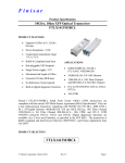
10G
Gb/s Indu
ustrial Teemperatu
ure 40km
m Datacom
m
SFP+ Transceiiver
FTLX1671D3B
BTL
PRO
ODUCT FEA
ATURES
•
Hot-plugg
gable SFP+ footprint
f
•
Supports 9.95 to 10.3Gb/s bit ratees
•
1
Power disssipation < 1.5W;
Typical <1W
<
•
RoHS-6 compliant
c
(leead-free)
•
Industriall temperaturee range
-40°C to 85°C
8
•
Single 3.3
3V power suupply
•
Maximum
m link lengthh of 40km
Preliminnary photo show
wn.
•
1550nm cooled
c
CML
L
technolog
gy
•
Receiver limiting elecctrical
interface
•
Duplex LC connectorr
•
Built-in digital
d
diagnoostic functions
TM
APPL
LICATIONS
S
•
100GBASE-ER
R/EW 10G Ethernet
E
Finisar’s FTLX1
1671D3BTL
L 10Gb/s Enhanced
E
Sm
mall Form Factor Plugggable SFP
P+
transcceivers are designed foor use in 10--Gigabit Ethhernet links up to 40km
m over singlle
modee fiber. They
T
are coompliant wiith SFF-843311, SFF-844322 and IE
EEE 802.3aae
10GB
BASE-ER/EW3. The FT
TLX1671D3B
BTL incorpoorates advannced CML™
™ technologyy,
and is
i a “limitin
ng module”, i.e., it empploys a limitting receiverr. Host boaard designerrs
usingg an EDC PHY IC shouuld follow thhe IC manuufacturer’s reecommendedd settings foor
interooperating the host-boardd EDC PHY
Y with a lim
miting receivver SFP+ moodule. Digitaal
diagnnostics functtions are avvailable via a 2-wire seerial interfacce, as speciified in SFF
F4
5
8472 . The transcceiver is RooHS compliaant and lead free per Dirrective 20022/95/EC , annd
Finisar Applicatio
on Note AN
N-20386.
PRO
ODUCT SEL
LECTION
FTLX11671D3B
BTL
© Finiisar Corporatio
on - February 2011
2
Rev. A0
Page 1
FTLX
X1671D3BCL SFP+ ER/EW
W Preliminary Specification
S
– February 20111
I.
Pin Descrriptions
Pin
1
2
3
4
5
6
7
8
9
10
11
12
13
14
15
16
17
18
19
20
Symbol
VEET
TFAULT
TDIS
SDA
SCL
MOD_ABS
RS0
RX_LOS
RS1
VEER
VEER
RDRD+
VEER
VCCR
VCCT
VEET
TD+
TDVEET
Name/Deescription
Transmittter Ground
Transmittter Fault
Transmittter Disable. Laaser output dissabled on high or open.
2-wire Serial Interface Data Line
2-wire Serial Interface Clock Line
Module Absent.
A
Grounnded within thee module
Rate Seleect 0.
Loss of Signal
S
indicatioon. Logic 0 inndicates normall operation.
Rate Seleect 1.
Receiverr Ground
Receiverr Ground
Receiverr Inverted DAT
TA out. AC Cooupled.
Receiverr Non-inverted DATA out. AC
A Coupled.
Receiverr Ground
Receiverr Power Supplyy
Transmittter Power Suppply
Transmittter Ground
Transmittter Non-Invertted DATA in. AC Coupled.
Transmittter Inverted DATA
D
in. AC Coupled.
C
Transmittter Ground
Ref.
R
1
2
3
2
2
2
4
5
4
1
1
1
1
1
Notes::
1. Circuit
C
ground is
i internally isoolated from chaassis ground.
2. T
is an opeen collector/draain output, which should be pulled
p
up with a 4.7k – 10k Ohms
O
resistor on
F
FAULT
3.
4.
5.
thhe host board iff intended for use.
u Pull up vooltage should bee between 2.0V
V to Vcc + 0.3V
V. A high
ouutput indicates a transmitter fault
f
caused byy either the TX
X bias current or the TX outpuut power
exxceeding the prreset alarm thresholds. A low
w output indicaates normal opeeration. In the low
l state, the
ouutput is pulled to <0.8V.
Laser output dissabled on TDIS >2.0V
>
or openn, enabled on TDIS <0.8V.
Innternally pulled
d down per SFF
F-8431 Rev 4.1.
LOS is open colllector output. Should be pullled up with 4.77k – 10kΩ on host
h board to a voltage
beetween 2.0V an
nd 3.6V. Logicc 0 indicates noormal operationn; logic 1 indiccates loss of siggnal.
Towards
Bezel
1
V
VeeT
2
T
TX_Fault
3
T
TX_Disable
4
S
SDA
5
S
SCL
6
M
MOD_ABS
7
R
RS0
8
R
RX_LOS
9
10
VeeT
20
TD-
19
TD+
18
VeeT
17
VccT
16
VccR
15
VeeR
14
RD+
13
RD-
12
VeeR
11
Towa
ards
ASIIC
R
RS1
V
VeeR
Figure 1. Diagram of
o Host Board Connector Bllock Pin Numb
bers and Nam
mes.
© Finiisar Corporatio
on - February 2011
2
Rev. A0
Page 2
FTLX
X1671D3BCL SFP+ ER/EW
W Preliminary Specification
S
– February 20111
II. Absolute
A
Maximum
M
Raatings
Exceeding the lim
mits below may
m damage the transceiver module permanentlyy.
Pa
arameter
Maxim
mum Supply Voltage
V
Storagge Temperaturee
Relativve Humidity
1.
III.
Symbol
Vcc
TS
RH
Min
-0.5
-40
0
Typ
p
Max
4.0
85
85
Unit
V
°C
%
R
Ref.
Max
3.46
400
Unit
V
mA
R
Ref.
Ω
mV
V
V
1
700
Vcc
Vee+ 0.8
mV
ps
V
V
mVpp
2,6
3
4
4
5
1
N
Non-condensing
g.
Electrical Characteriistics (TOP = -40
- to 85 °C, VCC = 3.14 to 3.46
3 Volts)
Parrameter
Supplyy Voltage
Supplyy Current
Transsmitter
Input differential
d
imp
pedance
Differrential data inpu
ut swing
Transm
mit Disable Vo
oltage
Transm
mit Enable Volltage
Receivver
Differrential data outp
put swing
Outpuut rise time and
d fall time
LOS Fault
F
LOS Normal
N
Powerr Supply Noisee Tolerance
Symbol
Vcc
Icc
Rin
Vin,pp
VD
VEN
Vout,pp
Tr, Tf
VLOS fault
VLOS norm
V
VccT/VccR
Min
3.14
Typ
p
2700
1000
180
2
Vee
300
850
28
2
VccHOST
Vee
Vee+0.8
Per SFF-8431 Rev 4.1
Notes::
1. Connected
C
direcctly to TX dataa input pins. AC coupling froom pins into lasser driver IC.
2. Innto 100Ω differrential terminaation.
3. 20
0 – 80%. Meaasured with Moodule Compliannce Test Boardd and OMA tesst pattern. Use of four 1’s andd
foour 0’s sequencce in the PRBS
S 9 is an accepttable alternativve.
4. LOS is an open collector outpuut. Should be pulled
p
up withh 4.7kΩ – 10kΩ
Ω on the host board.
b
Normal
opperation is logiic 0; loss of siggnal is logic 1.
5. Seee Section 2.8..4 of SFF-84311 Rev 4.1.
6. Thhe FTLX1671D
D3BTL is a “liimiting modulee”, i.e., it emplloys a limiting receiver. Host board designeers
ussing an EDC PHY
P
IC should follow the IC manufacturer’s recommendeed settings for interoperating
i
thhe host-board EDC
E
PHY withh a limiting recceiver SFP+ moodule.
IV.
Optical Characterist
C
tics (TOP = -40 to 85 °C, VCC3
= 3.14 to 3..46 Volts)
C
Parameeter
Transsmitter
Opticaal Modulation Amplitude
A
(OMA
A) minus TDP
Averaage Launch Pow
wer
Opticaal Wavelength
Side-M
Mode Suppresssion Ratio
Opticaal Extinction Ratio
R
Transm
mitter and Disp
persion Penaltyy
Averaage Launch pow
wer of OFF
transm
mitter
Tx Jittter
Relativve Intensity No
oise
© Finiisar Corporatio
on - February 2011
2
Symboll
Min
POMA-TDPP
-2.1
PAVE
λ
SMSR
ER
TDP
-4.7
1530
30
3.0
POFF
Txj
RIN
Typ
Max
Reff.
dBm
+4.0
1565
3.0
dBm
nm
dB
dB
dB
-30
dBm
Per 802.3ae reequirements
-128
Rev. A0
Unit
1
dB/Hz
Page 3
FTLX
X1671D3BCL SFP+ ER/EW
W Preliminary Specification
S
– February 20111
Receivver
Receivver Sensitivity (OMA)
@ 10.3 Gb/s
Stressed Receiver Seensitivity
A) @ 10.3 Gb/ss
(OMA
Averaage Receive Power
Damagge Threshold
Opticaal Center Waveelength
Receivver Reflectancee
LOS De-Assert
D
LOS Assert
A
LOS Hysteresis
H
RSENS1
-14.1
dBm
2
RSENS2
-11.3
dBm
3
-1.0
+4
1600
-26
-19
dBm
dBm
nm
dB
dBm
dBm
dB
4
PAVE
-15.8
λC
Rrx
LOSD
LOSA
1260
-28
0.5
Notes::
1. Average
A
launch power (min) is informative and
a not the prinncipal indicatoor of signal streength. A
transmitter with
h launch power below this vallue cannot be compliant;
c
how
wever, a value above
a
this doess
noot ensure comp
pliance.
2. Valid
V
between 1530
1
and 1565 nm. Measuredd with worst ER
R; BER<10-12; 231 – 1 PRBS..
3. Valid
V
between 1530
1
and 1565 nm. Per IEEE 802.3ae.
4. Average
A
power figures are info
formative only, per IEEE 802.3ae.
V.
General Sp
pecificationss
Param
meter
Symboll
BR
BER
LMAX
Bit Raate
Bit Errror Ratio
Max. Supported
S
Link
k Length
Min
9.95
Typ
Max
10.3
10-12
40
Units
Gb/s
km
Reff.
1
2
3
Notes::
1. 100GBASE-ER, 10GBASE-EW
W.
3
2. Tested with a 231
– 1 PRBS.
3. SM
MF-28 fiber, 1565nm waveleength.
Poweer Level I/P
Power Level II Power-u
up Sequencee
The FTLX1671D
F
D3BTL is a Power
P
Levell II device, as the maxim
mum power dissipation
d
iss
abovee 1W at high
h temperaturre. Please reefer to SFF-88431 and Finnisar Applicaation Note
AN-22076 for detaails of the hoost responsibbilities regarrding the Pow
wer Level I/P
Power Level
II pow
wer-up sequ
uence to ensuure proper traansceiver opperation.
Timiing Parametters
Parametter
Time to
t initialize coo
oled module
Symboll
t_start_up_coooled
Min
Typ
60
Max
90
Units
s
Reff.
1
Notes::
1. More
M
details on Timing Param
meters can be foound in SFF-84431. Maximum
m Tx_Disable negate
n
time
t__on = 3 second
ds.
© Finiisar Corporatio
on - February 2011
2
Rev. A0
Page 4
FTLX
X1671D3BCL SFP+ ER/EW
W Preliminary Specification
S
– February 20111
VI. Environme
E
ntal Specifiications
Finisar FTLX167
71D3BTL traansceivers have
h
an operaating temperrature range from -40°C
to +885°C case tem
mperature.
Param
meter
Case Operating
O
Tem
mperature
Storagge Temperaturee
VII.
Symboll
Top
Tsto
Min
-40
-40
Typ
Max
85
85
Units
°C
°C
Reff.
Regulato
ory Compliaance
Finisar transceiveers are Classs 1 Laser Prooducts and coomply with US FDA reggulations.
Thesee products arre certified by
b TÜV andd CSA to meet the Class 1 eye safetyy
requiirements of EN
E (IEC) 600825 and the electrical saafety requireements of
EN (IIEC) 60950. Copies of certificates
c
a availablee at Finisar Corporation
are
C
u
upon
request.
D
Fu
unctions
VIII.. Digital Diagnostic
Finisar FTLX167
71D3BTL SF
FP+ transceiivers supporrt the 2-wire serial comm
munication
protoocol as defineed in the SFP
P MSA1. It is
i very closeely related too the E2PROM
M defined inn
the GBIC
G
standarrd, with the same
s
electrical specificaations.
s
SFP
P serial ID provides acceess to identiffication inforrmation thatt describes
The standard
the trransceiver’s capabilities,, standard intterfaces, maanufacturer, and
a other infformation.
Addittionally, Fin
nisar SFP+ trransceivers provide
p
a enhhanced digittal diagnostic monitoringg
interfface, which allows
a
real-ttime access to
t device operating parameters such as
transcceiver tempeerature, laserr bias currennt, transmitteed optical poower, receiveed optical
poweer and transcceiver supplyy voltage. It also definess a sophisticaated system of alarm andd
warning flags, wh
hich alerts ennd-users whhen particularr operating parameters
p
a outside of
are
o
a facttory set norm
mal range.
The SFP
S MSA deefines a 256--byte memorry map in E2PROM thatt is accessiblle over a
2-wirre serial interrface at the 8 bit addresss 1010000X (A0h). The digital diagnnostic
moniitoring interfface makes use
u of the 8 bit
b address 1010001X (A
A2h), so the originally
definned serial ID memory maap remains unchanged.
u
T interfacee is identicall to, and is
The
thus fully
f
backwaard compatibble with bothh the GBIC Specificationn and the SF
FP Multi
Sourcce Agreemen
nt. The compplete interface is describbed in Finisaar Applicatioon Note AN-2030: “Digital Diiagnostics Monitoring
M
Innterface for SFP
S Optical Transceiverrs”.
The operating
o
and diagnosticcs informatioon is monitorred and repoorted by a Diigital
Diagnnostics Tran
nsceiver Conntroller (DDT
TC) inside thhe transceiveer, which is accessed
a
throuugh a 2-wire serial interfa
face. When thhe serial prootocol is activvated, the seerial clock
signaal (SCL, Mod
d Def 1) is generated
g
by the host. Thhe positive edge
e
clocks data into thee
SFP transceiver
t
into
i
those segments of thhe E2PROM that are not write-proteccted. The
negattive edge clo
ocks data froom the SFP transceiver.
t
The serial data
d signal (S
SDA, Mod
© Finiisar Corporatio
on - February 2011
2
Rev. A0
Page 5
FTLX
X1671D3BCL SFP+ ER/EW
W Preliminary Specification
S
– February 20111
Def 2)
2 is bi-direcctional for seerial data trannsfer. The hoost uses SDA
A in conjuncction with
SCL to mark the start and endd of serial prrotocol activvation. The memories
m
aree organized
as a series
s
of 8-biit data wordss that can bee addressed individually
i
or sequentiaally.
m
informaation, pleasee see the SFP
P MSA docuumentation1,55 and Finisarr Applicationn
For more
Note AN-2030.
Pleasse note that evaluation
e
booard FDB-10027 is availaable with Finnisar ModDE
EMO
softw
ware that allo
ows simple too use communication ovver the 2-wirre serial interrface.
agnostic Speecifications
IX. Digital Dia
X1671D3BT
TL transceiveers can be ussed in host systems
s
that require eitheer internally
FTLX
or externally calib
brated digitaal diagnosticcs.
Param
meter
Symbool
Accu
uracy
Internnally measured transceiver
ΔDDTempeerature
tempeerature
Internnally measured transceiver
ΔDDVolttage
supplyy voltage
Measuured TX bias current
c
ΔDDBiaas
Measuured TX outpu
ut power
ΔDDTx-Poower
Measuured RX receiv
ved average
ΔDDRx-Poower
opticaal power
Dynaamic Range fo
or Rated Accu
uracy
Internnally measured transceiver
DDTemperaature
tempeerature
Internnally measured transceiver
DDVoltage
supplyy voltage
Measuured TX bias current
c
DDBiass
Measuured TX outpu
ut power
DDTx-Powwer
Measuured RX receiv
ved average
DDRx-Powwer
opticaal power
Min
Typ
Max
Units
3
ºC
3
%
10
2
2
%
dB
dB
-40
85
ºC
3.1
3.5
V
0
-4.7
-15.8
100
+4.0
-1.0
mA
dBm
dBm
Reff.
1
Notes::
1. Accuracy of meassured Tx bias current
c
is 10% of the actual bias
b current froom the laser driiver to the laserr.
© Finiisar Corporatio
on - February 2011
2
Rev. A0
Page 6
FTLX
X1671D3BCL SFP+ ER/EW
W Preliminary Specification
S
– February 20111
X.
M
Mechanical
l Specificatiions
Finisar FTLX167
71D3BTL SF
FP+ transceiivers are com
mpatible withh the SFF-84432
speciification for improved plluggable form
m factor, andd shown herre for referennce purposess
only. To allow fo
or potential heat-sink
h
appplications, thhe label is on the bottom
m side. Bail
colorr is red.
Figure
F
2. FTLX1671D
F
D3BTL Mech
hanical Dim
mensions
© Finiisar Corporatio
on - February 2011
2
Rev. A0
Page 7
FTLX
X1671D3BCL SFP+ ER/EW
W Preliminary Specification
S
– February 20111
XI. PCB Layou
ut and Bezeel Recommeendations
Figure 3
© Finiisar Corporatio
on - February 2011
2
Rev. A0
Page 8
FTLX
X1671D3BCL SFP+ ER/EW
W Preliminary Specification
S
– February 20111
Figure 4
© Finiisar Corporatio
on - February 2011
2
Rev. A0
Page 9
FTLX
X1671D3BCL SFP+ ER/EW
W Preliminary Specification
S
– February 20111
XII.
Host-Modulee Interface Diagram
D
Figure 5
© Finiisar Corporatio
on - February 2011
2
Rev. A0
Page 110
FTLX
X1671D3BCL SFP+ ER/EW
W Preliminary Specification
S
– February 20111
XIII. Reeferences
1. “S
Specification
ns for Enhannced 8.5 andd 10 Gigabit Small Form
m Factor Plugggable
M
Module
‘SFP
P+ ‘”, SFF Document Nuumber SFF-88431, Revision 4.1, July 6, 2009.
A
Although
SFF
F-8431 doess not explicittly refer to 10GBASE-ER
R/EW, it is intended
i
forr
thhe FTLX167
71D3BTL prroduct to adhhere to refereences to elecctrical SFI sppecificationss
siimilar to 10G
GBASE-LR//LW.
2.
““Improved Pluggable
P
Foormfactor”, SFF
S Documeent Number SFF-8432, Revision
R
4.22,
A
April
18, 200
07.
3. IE
EEE Std 802
2.3ae, Clausee 52, PMD Type
T
10GBA
ASE-ER. IE
EEE Standardds
D
Department.
4. “D
Digital Diag
gnostics Monnitoring Interrface for Opptical Transceivers”. SFF
F Documentt
N
Number
SFF--8472, Revission 10.1, March
M
1, 20077.
5. D
Directive 200
02/95/EC off the Europeean Council Parliament and of the Council, “oon
thhe restriction
n of the use of certain hazardous
h
suubstances inn electrical and
a electroniic
eqquipment”. January
J
27, 2003.
2
6. “A
Application Note AN-20038: Finisar Implementaation Of RoH
HS Compliannt
T
Transceivers”
”, Finisar Coorporation, January 21, 2005.
2
XIV.. For Moree Information
Finisar Corporatiion
1389 Moffett Parrk Drive
Sunnnyvale, CA 94089-1133
9
Tel. 1-408-548-1
1
000
Fax 1-408-541-6
1
138
sales@
@finisar.com
m
www
w.finisar.com
m
© Finiisar Corporatio
on - February 2011
2
Rev. A0
Page 11
1