1
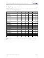
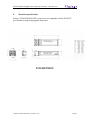
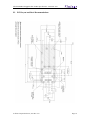
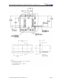
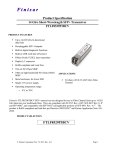
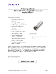
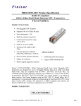
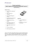
Product Specification 14 Gb/s Short-Wavelength SFP+ Transceiver FTLF8529P3BNV PRODUCT FEATURES Up to 14.025 Gb/s bi-directional data links Hot-pluggable SFP+ footprint Built-in digital diagnostic functions Built-in CDR with shut off control 850nm Oxide VCSEL laser transmitter Duplex LC connector RoHS compliant and Lead Free 35m on 50/125μm MMF 100m on high-bandwidth 50/125um (OM3) MMF Metal enclosure, for lower EMI Single 3.3V power supply Operating temperature range: APPLICATIONS Tri-Rate 4.25/8.5/14.025 Gb/s Fibre Channel o 0°C to 85°C Finisar’s FTLF8529P3BNV SFP+ transceivers are designed for use in Fibre Channel links up to 14.025 Gb/s data rate over multimode fiber. They are compliant with FC-PI-5 Rev. 6.00a, SFF-8472 Rev 11.0c and SFF-8081h, and compatible with SFF-8432b and applicable portions of SFF-8431 Rev. 4.1d. The product is RoHS compliant and lead-free per Directive 2002/95/ECe and Finisar Application Note AN2038. PRODUCT SELECTION FTLF8529P3BNV © Finisar Corporation Dec 8, 2011 Rev. 2.5 Page 1 FTLF8529P2BxV Pluggable SFP+ Product Specification – December 2011 4. Pin Descriptions Pin 1 2 3 4 5 6 7 Symbol VEET TFAULT TDIS SDA SCA MOD_ABS RS0 8 9 LOS RS1 10 11 12 13 14 15 16 17 18 19 20 VEER VEER RDRD+ VEER VCCR VCCT VEET TD+ TDVEET Name/Description Transmitter Ground (Common with Receiver Ground) Transmitter Fault. Transmitter Disable. Laser output disabled on high or open. 2-wire Serial Interface Data Line (MOD-DEF2) 2-wire Serial Interface Clock (MOD-DEF1) Module Absent, connected to VEET or VEER Rx Rate Select: Open or Low = 8.5 or 4.25 Gb/s Fibre Channel (Low Bandwidth) High = 14.025 Gb/s Fibre Channel (High Bandwidth) Loss of Signal indication. Logic 0 indicates normal operation. Tx Rate Select: Open or Low = 8.5 or 4.25 Gb/s Fibre Channel (Low Bandwidth) High = 14.025 Gb/s Fibre Channel (High Bandwidth) Receiver Ground (Common with Transmitter Ground) Receiver Ground (Common with Transmitter Ground) Receiver Inverted DATA out. AC Coupled Receiver Non-inverted DATA out. AC Coupled Receiver Ground (Common with Transmitter Ground) Receiver Power Supply Transmitter Power Supply Transmitter Ground (Common with Receiver Ground) Transmitter Non-Inverted DATA in. AC Coupled. Transmitter Inverted DATA in. AC Coupled. Transmitter Ground (Common with Receiver Ground) Ref. 1 2 3 4 4 4 5 6 5 1 1 1 1 1 Notes: 1. Circuit ground is internally isolated from chassis ground. 2. TFAULT is an open collector/drain output, which should be pulled up with a 4.7k – 10k Ohms resistor on the host board if intended for use. Pull up voltage should be between 2.0V to Vcc + 0.3V. A high output indicates a transmitter fault caused by either the TX bias current or the TX output power exceeding the preset alarm thresholds. A low output indicates normal operation. In the low state, the output is pulled to <0.8V. 3. Laser output disabled on TDIS >2.0V or open, enabled on TDIS <0.8V. 4. Should be pulled up with 4.7k – 10kohms on host board to a voltage between 2.0V and 3.6V. MOD_ABS pulls line low to indicate module is plugged in. 5. Rate select can also be set through the 2-wire bus in accordance with SFF-8472 v. 11.0c. Rx Rate Select is set at Bit 3, Byte 110, Address A2h. Tx Rate Select is set at Bit 3, Byte 118, Address A2h. Note: writing a “1” selects maximum bandwidth operation. Rate select is the logic OR of the input state of Rate Select Pin and 2-wire bus. 6. LOS is open collector output. Should be pulled up with 4.7k – 10kohms on host board to a voltage between 2.0V and 3.6V. Logic 0 indicates normal operation; logic 1 indicates loss of signal. © Finisar Corporation Dec 8, 2011 Rev. A.0 Page 2 FTLF8529P2BxV Pluggable SFP+ Product Specification – December 2011 Diagram of Host Board Connector Block Pin Numbers and Names 4. Absolute Maximum Ratings Parameter Maximum Supply Voltage Storage Temperature Case Operating Temperature Relative Humidity (Non-condensing) © Finisar Corporation Dec 8, 2011 Rev. A.0 Symbol Vcc TS TC RH Min -0.5 -40 0 0 Typ Max 4.0 85 85 85 Unit V °C °C % Ref. Page 3 FTLF8529P2BxV Pluggable SFP+ Product Specification – December 2011 III. Electrical Characteristics (Tc, VCC = 3.15 to 3.46 Volts) Parameter Supply Voltage Supply Current Transmitter Input differential impedance Single ended data input swing Transmit Disable Voltage Transmit Enable Voltage Receiver Single ended data output swing LOS Fault LOS Normal Power Supply Rejection Deterministic Jitter @ 8.5 Gb/s Deterministic Jitter @ 14.025 Gb/s Symbol Vcc Icc Rin Vin,pp VD VEN Vout,pp VLOS fault VLOS norm PSR RX DJ RX DJ Min 3.15 Typ Max 3.46 285 Unit V mA 2 90 2 Vee 800 Vcc Vee+ 0.8 Ω mV V V 185 2 Vee 100 425 VccHOST Vee+0.8 mV V V mVpp UI UI 4 5 5 6 100 0.420 0.220 Ref. 1 3 Notes: 1. With established link 2. Connected directly to TX data input pins. AC coupling from pins into laser driver IC. 3. Or open circuit. 4. Into 100 ohms differential termination. 5. LOS is an open collector output. Should be pulled up with 4.7k – 10kohms on the host board. Normal operation is logic 0; loss of signal is logic 1. Maximum pull-up voltage is 5.5V. 6. Receiver sensitivity is compliant with power supply sinusoidal modulation of 20 Hz to 1.5 MHz up to specified value applied through the recommended power supply filtering network. © Finisar Corporation Dec 8, 2011 Rev. A.0 Page 4 FTLF8529P2BxV Pluggable SFP+ Product Specification – December 2011 VI. Optical Characteristics (TA, VCC = 3. 15 to 3.46 Volts) Parameter Transmitter Avergare Output Output. Power: 50 or 62.5 MMF Optical Wavelength Spectral Width (RMS) @ 14.025Gb/s Optical Modulation Amplitude @ 4.25 Gb/s Optical Modulation Amplitude @ 8.5 Gb/s Optical Modulation Amplitude @ 14.025 Gb/s Optical Rise/Fall Time @ 4.25 Gb/s Transmitter Waveform and Dispersion Penalty @ 8.5 Gb/s Vertical Eye Closure Penalty @ 14.025 Gb/s Relative Intensity Noise Receiver Receiver OMA Sensitivity = 4.25 Gb/s Receiver OMA Sensitivity = 8.5 Gb/s Receiver OMA Sensitivity = 14.025 Gb/s Average Receiver Power Optical Center Wavelength Optical Return Loss LOS De-Assert LOS Assert LOS Hysteresis Symbol Min POUT -7.8 λ σ OMA OMA OMA tr/ tf TWDP 840 Unit Ref. dBm 1 90 4.3 nm nm μW μW μW ps dB 2 3 CEVPQ RIN 2.56 -128 dB dB/Hz 4 RxSENS RxSENS RxSENS RxMAX λC 61 76 89 μW μW μW dBm nm dB dBm dBm dB 5 5 5 LOSD LOSA Typ Max 860 0.59 247 302 331 0 770 12 860 -13 -30 0.5 Notes: 1. Class 1 Laser Safety limit per FDA/CDRH, and EN (IEC) 60825 laser safety standards. 2. Unfiltered, 20-80%. Complies with FC 1x and 2x eye mask when filtered. 3. TWDP is calculated with a 1,0 equalizer and a 9.84 GHz Gaussian filter for the fiber simulation. Jitter values at γT and γR are controlled by TWDP and stress receiver sensitivity. 4. VECPQ is calculated with a 16.6 GHz Gaussian filter for fiber simulation 5. Unstressed Rx sensitivity © Finisar Corporation Dec 8, 2011 Rev. A.0 Page 5 FTLF8529P2BxV Pluggable SFP+ Product Specification – December 2011 General Specifications VI. Parameter Data Rate Symbol BR Bit Error Rate Fiber Length on 50/125μm MMF BER L Fiber Length on 50/125μm highbandwidth (OM3) MMF L Min Typ 4.25, 8.5 14.025 Max 10-12 150 50 35 380 150 100 Units Gb/sec m m Ref. 1 2 3 4 5 3 4 5 Notes: 1. 4x and 8x Fibre Channel compatible, per FC-PI-41. 2. PRBS 27-1 for 4GFC and 8GFC. PRBS 231-1 for 16GFC 3. At 4.25 Gb/s Fibre Channel data rate. 4. At 8.5 Gb/s Fibre Channel data rate. 5. At 14.025 Gb/s Fibre Channel data rate. VI. Environmental Specifications Parameter Case Operating Temperature Commercial Temperature Extended Temperature Storage Temperature VII. Symbol Top Tsto Min 0 0 -40 Typ Max 70 85 85 Units °C Ref. °C Regulatory Compliance Finisar transceivers are Class 1 Laser Products and comply with US FDA regulations. These products are certified by TÜV and CSA to meet the Class 1 eye safety requirements of EN (IEC) 60825 and the electrical safety requirements of EN (IEC) 60950. Copies of certificates are available at Finisar Corporation upon request. © Finisar Corporation Dec 8, 2011 Rev. A.0 Page 6 FTLF8529P2BxV Pluggable SFP+ Product Specification – December 2011 VIII. Digital Diagnostic Functions Finisar FTLF8529P3BNV SFP+ transceivers support the 2-wire serial communication protocol as defined in the SFP MSAf. It is very closely related to the E2PROM defined in the GBIC standard, with the same electrical specifications. The standard SFP serial ID provides access to identification information that describes the transceiver’s capabilities, standard interfaces, manufacturer, and other information. Additionally, Finisar SFP transceivers provide a enhanced digital diagnostic monitoring interface, which allows real-time access to device operating parameters such as transceiver temperature, laser bias current, transmitted optical power, received optical power and transceiver supply voltage. It also defines a sophisticated system of alarm and warning flags, which alerts end-users when particular operating parameters are outside of a factory set normal range. The SFP MSA defines a 256-byte memory map in E2PROM that is accessible over a 2-wire serial interface at the 8 bit address 1010000X (A0h). The digital diagnostic monitoring interface makes use of the 8 bit address 1010001X (A2h), so the originally defined serial ID memory map remains unchanged. The interface is identical to, and is thus fully backward compatible with both the GBIC Specification and the SFP Multi Source Agreement. The complete interface is described in Finisar Application Note AN-2030: “Digital Diagnostics Monitoring Interface for SFP Optical Transceivers”. The operating and diagnostics information is monitored and reported by a Digital Diagnostics Transceiver Controller (DDTC) inside the transceiver, which is accessed through a 2-wire serial interface. When the serial protocol is activated, the serial clock signal (SCL, Mod Def 1) is generated by the host. The positive edge clocks data into the SFP transceiver into those segments of the E2PROM that are not write-protected. The negative edge clocks data from the SFP transceiver. The serial data signal (SDA, Mod Def 2) is bi-directional for serial data transfer. The host uses SDA in conjunction with SCL to mark the start and end of serial protocol activation. The memories are organized as a series of 8-bit data words that can be addressed individually or sequentially. For more information, please see the SFP MSA documentationc,f and Finisar Application Note AN2030. Please note that evaluation board FDB-1027 is available with Finisar ModDEMO software that allows simple to use communication over the 2-wire serial interface. © Finisar Corporation Dec 8, 2011 Rev. A.0 Page 7 FTLF8529P2BxV Pluggable SFP+ Product Specification – December 2011 IX. Digital Diagnostic Specifications FTLF8529P3BNV transceivers can be used in host systems that require either internally or externally calibrated digital diagnostics. Parameter Symbol Accuracy DDTemperature Internally measured transceiver temperature DDVoltage Internally measured transceiver supply voltage DDBias Measured TX bias current DDTx-Power Measured TX output power DDRx-Power Measured RX received average optical power Dynamic Range for Rated Accuracy DDTemperature Internally measured transceiver temperature DDVoltage Internally measured transceiver supply voltage DDBias Measured TX bias current DDTx-Power Measured TX output power DDRx-Power Measured RX received average optical power Max Reporting Range DDTemperature Internally measured transceiver temperature DDVoltage Internally measured transceiver supply voltage DDBias Measured TX bias current DDTx-Power Measured TX output power DDRx-Power Measured RX received average optical power Min Typ Max Units 3 ºC 100 mV 10 2 2 % dB dB -0 85 ºC 3.15 3.46 V 0 -8 -14 20 -1 0 mA dBm dBm -40 125 ºC 2.8 4.0 V 0 -10 -20 20 -2 0 mA dBm dBm Ref. 1 Notes: 1. Accuracy of Measured Tx Bias Current is 10% of the actual Bias Current from the laser driver to the laser. © Finisar Corporation Dec 8, 2011 Rev. A.0 Page 8 FTLF8529P2BxV Pluggable SFP+ Product Specification – December 2011 X. Mechanical Specifications Finisar’s FTLF8529P3BNV SFP+ transceivers are compatible with the SFF-8432b specification for improved pluggable form factor. FTLF8529P3BNV © Finisar Corporation Dec 8, 2011 Rev. A.0 Page 9 FTLF8529P2BxV Pluggable SFP+ Product Specification – December 2011 XI. PCB Layout and Bezel Recommendations © Finisar Corporation Dec 8, 2011 Rev. A.0 Page 10 FTLF8529P2BxV Pluggable SFP+ Product Specification – December 2011 © Finisar Corporation Dec 8, 2011 Rev. A.0 Page 11 FTLF8529P2BxV Pluggable SFP+ Product Specification – December 2011 XII. References a. “Fibre Channel Physical Interface-4 Specification (FC-PI-5 Rev. 6.00)”. American National Standard for Information Systems, To Be Published. b. “Improved Pluggable Form Factor”, SFF Document Number SFF-8432, Revision 5.0, July 16, 2007. c. “Digital Monitoring Interface for Optical Transceivers”, SFF Document Number SFF-8472, Revision 11.0. d. “Enhanced Small Form Factor Pluggable Module ‘SFP+ ‘”, SFF Document Number SFF-8431, Revision 4.1, July 6, 2009. e. Directive 2002/95/EC of the European Council Parliament and of the Council, “on the restriction of the use of certain hazardous substances in electrical and electronic equipment.” January 27, 2003. f. Small Form Factor Pluggable (SFP) Transceiver Multi-source Agreement (MSA), September 14, 2000 which is available as SFF Document Number INF-8074, Revision 1.0 May 12, 2001 g. “0.8mm Card Edge Connector for 16Gb/s Applications”, SFF Document Number SFF-8081, Revision 0.2, December 21, 2009. h. SFF-8081, Revision 0.2, Revision 0.9 XIII. For More Information Finisar Corporation 1389 Moffett Park Drive Sunnyvale, CA 94089-1133 Tel. 1-408-548-1000 Fax 1-408-541-6138 [email protected] www.finisar.com © Finisar Corporation Dec 8, 2011 Rev. A.0 Page 12