1
4.4
4.5
4.6
4.7
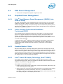
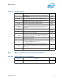
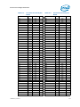
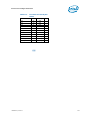
4.3.2.1 Initialization Role of CKE ............................................................ 54
4.3.2.2 Conditional Self-Refresh ............................................................ 54
4.3.2.3 Dynamic Power-down Operation ................................................. 54
4.3.2.4 DRAM I/O Power Management .................................................... 54
PCIe* Power Management .................................................................................. 54
DMI Power Management..................................................................................... 55
Graphics Power Management .............................................................................. 55
4.6.1 Intel® Rapid Memory Power Management (RMPM) (also know as CxSR) ........ 55
4.6.2 Intel® Graphics Performance Modulation Technology(GPMT) ........................ 55
4.6.3 Graphics Render C-State ......................................................................... 55
4.6.4 Intel® Smart 2D Display Technology (Intel® S2DDT) .................................. 55
4.6.5 Intel® Graphics Dynamic Frequency.......................................................... 56
Thermal Power Management ............................................................................... 56
5
Thermal Management .............................................................................................. 57
6
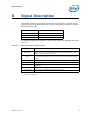
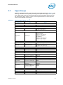
Signal Description ................................................................................................... 59
6.1
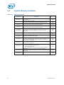
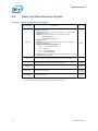
System Memory Interface .................................................................................. 60
6.2
Memory Reference and Compensation .................................................................. 61
6.3
Reset and Miscellaneous Signals.......................................................................... 62
6.4
PCI Express* Based Interface Signals................................................................... 63
6.5
Intel® Flexible Display Interface Signals ............................................................... 63
6.6
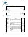
DMI................................................................................................................. 64
6.7
PLL Signals....................................................................................................... 64
6.8
TAP Signals ...................................................................................................... 64
6.9
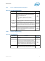
Error and Thermal Protection .............................................................................. 65
6.10 Power Sequencing ............................................................................................. 65
6.11 Processor Power Signals ..................................................................................... 66
6.12 Sense Pins ....................................................................................................... 66
6.13 Ground and NCTF .............................................................................................. 66
6.14 Processor Internal Pull Up/Pull Down.................................................................... 67
7
Electrical Specifications ........................................................................................... 69
7.1
Power and Ground Lands.................................................................................... 69
7.2
Decoupling Guidelines ........................................................................................ 69
7.2.1 Voltage Rail Decoupling........................................................................... 69
7.3
Processor Clocking (BCLK[0], BCLK#[0]) .............................................................. 70
7.3.1 PLL Power Supply ................................................................................... 70
7.4
VCC Voltage Identification (VID) .......................................................................... 70
7.5
System Agent (SA) VCC VID ............................................................................... 74
7.6
Reserved or Unused Signals................................................................................ 74
7.7
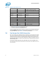
Signal Groups ................................................................................................... 75
7.8
Test Access Port (TAP) Connection....................................................................... 76
7.9
Storage Conditions Specifications ........................................................................ 77
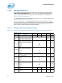
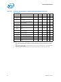
7.10 DC Specifications .............................................................................................. 78
7.10.1 Voltage and Current Specifications............................................................ 78
7.11 Platform Environmental Control Interface (PECI) DC Specifications........................... 84
7.11.1 PECI Bus Architecture ............................................................................. 84
7.11.2 DC Characteristics .................................................................................. 85
7.11.3 Input Device Hysteresis .......................................................................... 85
8
Processor Pin and Signal Information...................................................................... 87
8.1
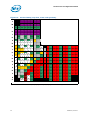
Processor Pin Assignments ................................................................................. 87
9
DDR Data Swizzling ............................................................................................... 107
Datasheet, Volume 1
5