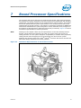
1
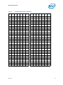
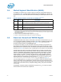
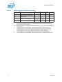
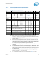
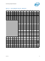
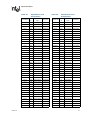
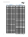
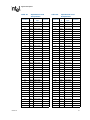
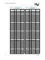
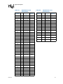
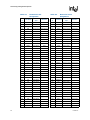
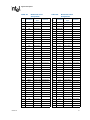
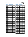
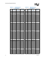
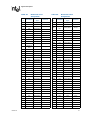
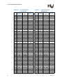
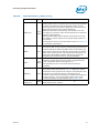
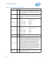
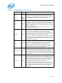
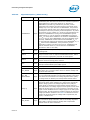
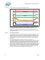
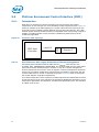
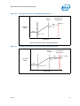
Electrical Specifications
2.2.3
FSB Decoupling
The processor integrates signal termination on the die. In addition, some of the high
frequency capacitance required for the FSB is included on the processor package.
However, additional high frequency capacitance must be added to the motherboard to
properly decouple the return currents from the front side bus. Bulk decoupling must
also be provided by the motherboard for proper [A]GTL+ bus operation.
2.3
Voltage Identification
The Voltage Identification (VID) specification for the processor is defined by the Voltage
Regulator-Down (VRD) 11 Design Guide For Desktop and Transportable LGA775. The
voltage set by the VID signals is the reference VR output voltage to be delivered to the
processor VCC pins (see Chapter 2.6.3 for VCC overshoot specifications). Refer to
Table 13 for the DC specifications for these signals. Voltages for each processor
frequency is provided in Table 5.
Individual processor VID values may be calibrated during manufacturing such that two
devices at the same core speed may have different default VID settings. This is
reflected by the VID Range values provided in Table 5. Refer to the Intel® Celeron®
Processor 400 Series Specification Update for further details on specific valid core
frequency and VID values of the processor. Please note this differs from the VID
employed by the processor during a power management event (Thermal Monitor 2).
The processor uses six voltage identification signals, VID[6:1], to support automatic
selection of power supply voltages. Table 2 specifies the voltage level corresponding to
the state of VID[6:1]. A ‘1’ in this table refers to a high voltage level and a ‘0’ refers to
a low voltage level. If the processor socket is empty (VID[6:1] = 111111), or the
voltage regulation circuit cannot supply the voltage that is requested, it must disable
itself. The Voltage Regulator-Down (VRD) 11 Design Guide For Desktop and
Transportable LGA775 defines VID [7:0], VID7 and VID0 are not used on the
processor; VID0 and VID7 is strapped to VSS on the processor package. VID0 and VID7
must be connected to the VR controller for compatibility with future processors.
The processor provides the ability to operate while transitioning to an adjacent VID and
its associated processor core voltage (VCC). This will represent a DC shift in the load
line. It should be noted that a low-to-high or high-to-low voltage state change may
result in as many VID transitions as necessary to reach the target core voltage.
Transitions above the specified VID are not permitted. Table 5 includes VID step sizes
and DC shift ranges. Minimum and maximum voltages must be maintained as shown in
Table 6 and Figure 1 as measured across the VCC_SENSE and VSS_SENSE lands.
The VRM or VRD utilized must be capable of regulating its output to the value defined
by the new VID. DC specifications for dynamic VID transitions are included in Table 5
and Table 6. Refer to the Voltage Regulator-Down (VRD) 11 Design Guide For Desktop
and Transportable LGA775 for further details.
14
Datasheet