1
Figures
1
2
3
4
5
6
7
8
9
10
11
12
13
14
15
16
17
18
19
20
21
22
23
24
25
26
27
29
28
30
31
32
33
34
35
36
37
38
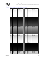
Datasheet
Second Level (L2) Cache Implementation ........................................................... 9
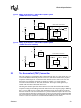
AGTL+ Bus Topology ..........................................................................................14
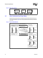
Stop Clock State Machine ...................................................................................14
BSEL[1:0] Example for a 100 MHz System Design (100 MHz Processor
Installed)..............................................................................................................22
BSEL[1:0] Example for a 100/133 MHz Capable System
(100 MHz Processor Installed) ............................................................................23
BSEL[1:0] Example for a 100/133 MHz Capable System
(133 MHz Processor Installed) ............................................................................23
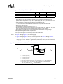
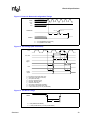
BCLK, PICCLK, and TCK Generic Clock Waveform...........................................37
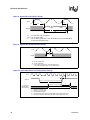
System Bus Valid Delay Timings ........................................................................38
System Bus Setup and Hold Timings..................................................................38
System Bus Reset and Configuration Timings....................................................38
Power-On Reset and Configuration Timings.......................................................39
Test Timings (TAP Connection) ..........................................................................39
Test Reset Timings .............................................................................................39
BCLK and PICCLK Generic Clock Waveform .....................................................40
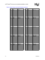
Maximum Acceptable AGTL+ and Non-AGTL+ Overshoot/Undershoot
Waveform ............................................................................................................46
Low to High AGTL+ and Non-AGTL+ Receiver Ringback Tolerance .................48
Signal Overshoot/Undershoot, Settling Limit, and Ringback...............................48
S.E.C.Cartridge — 3-Dimensional View..............................................................49
S.E.C.Cartridge 2 — Substrate View ..................................................................50
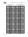
Processor Functional Die Layout (CPUID=0686h)..............................................52
Processor Functional Die Layout (up to CPUID=0683h).....................................52
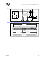
S.E.C.C. Packaged Processor — Multiple Views................................................54
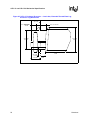
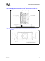
S.E.C.C. Packaged Processor — Extended Thermal Plate Side
Dimensions..........................................................................................................55
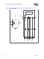
S.E.C.C. Packaged Processor — Bottom View Dimensions...............................55
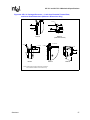
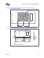
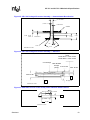
S.E.C.C. Packaged Processor — Latch Arm, Extended Thermal Plate Lug,
and Cover Lug Dimensions .................................................................................56
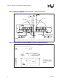
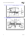
S.E.C.C. Packaged Processor — Latch Arm, Extended Thermal Plate,
and Cover Detail Dimensions (Reference Dimensions Only)..............................57
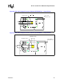
S.E.C.C. Packaged Processor — Extended Thermal Plate Attachment
Detail Dimensions ...............................................................................................58
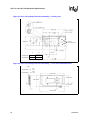
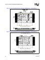
S.E.C.C. Packaged Processor Substrate — Edge Finger Contact
Dimensions..........................................................................................................59
S.E.C.C. Packaged Processor — Extended Thermal Plate Attachment
Detail Dimensions, Continued .............................................................................59
S.E.C.C. Packaged Processor Substrate — Edge Finger Contact
Dimensions, Detail A ...........................................................................................60
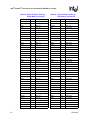
Intel® Pentium® III Processor Markings (S.E.C.C. Packaged Processor)...........60
S.E.C.C.2 Packaged Processor — Multiple Views..............................................61
S.E.C.C.2 Packaged Processor Assembly — Primary View...............................62
S.E.C.C.2 Packaged Processor Assembly — Cover View with Dimensions ......62
S.E.C.C.2 Packaged Processor Assembly — Heatsink Attach Boss Section.....63
S.E.C.C.2 Packaged Processor Assembly — Side View ....................................63
Detail View of Cover in the Vicinity of the Substrate Attach Features.................63
S.E.C.C.2 Packaged Processor Substrate — Edge Finger Contact
Dimensions..........................................................................................................64
5