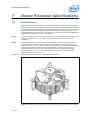
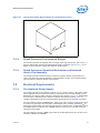
1
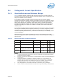
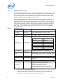
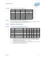
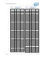
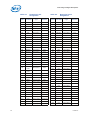
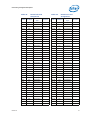
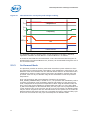
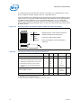
Electrical Specifications
Table 14.
GTL+ Bus Voltage Definitions
Symbol
Notes1
Parameter
Min
Typ
Max
Units
GTLREF_PU
GTLREF pull up on Intel®
3 Series Chipset family
boards
57.6 * 0.99
57.6
57.6 * 1.01
Ω
2
GTLREF_PD
GTLREF pull down on
Intel® 3 Series Chipset
family boards
100 * 0.99
100
100 * 1.01
Ω
2
RTT
Termination Resistance
45
50
55
Ω
3
COMP[3:0]
COMP Resistance
49.40
49.90
50.40
Ω
4
COMP8
COMP Resistance
24.65
24.90
25.15
Ω
4
NOTES:
1.
Unless otherwise noted, all specifications in this table apply to all processor frequencies.
2.
GTLREF is to be generated from VTT by a voltage divider of 1% resistors. If an Adjustable
GTLREF circuit is used on the board (for Quad-Core processors compatibility) the two
GTLREF lands connected to the Adjustable GTLREF circuit require the following:
GTLREF_PU = 50 Ω, GTLREF_PD = 100 Ω.
3.
RTT is the on-die termination resistance measured at VTT/3 of the GTL+ output driver.
4.
COMP resistance must be provided on the system board with 1% resistors. COMP[3:0] and
COMP8 resistors are to VSS.
2.8
Clock Specifications
2.8.1
Front Side Bus Clock (BCLK[1:0]) and Processor Clocking
BCLK[1:0] directly controls the FSB interface speed as well as the core frequency of the
processor. As in previous generation processors, the processor’s core frequency is a
multiple of the BCLK[1:0] frequency. The processor bus ratio multiplier will be set at its
default ratio during manufacturing. The processor supports Half Ratios between 7.5
and 13.5, refer to Table 15 for the processor supported ratios.
The processor uses a differential clocking implementation. For more information on the
processor clocking, contact your Intel field representative.
Datasheet
27