1
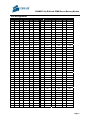
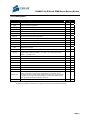
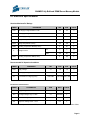
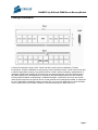
2048MB Fully Buffered DIMM Server Memory Module
CM75FB2048-667
Key Features
240-pin, Fully Buffered dual in-line memory module (FB-DIMM)
Ultra high density using 512 MBit SDRAM devices
CRC and ECC error detection and correction
Advanced Memory Buffer (AMB)
256 MB x 72
JEDEC standard1.5V high speed differential point-to-point link
Four-bit prefetch architecture
Off-chip driver (OCD) impedance calibration
On-die termination (ODT)
Low profile (1.2”), ideal for 1U rack mount servers
Selection Guide
CM75FB2048-667
MODULE SIZE:
2048 MByte
SPEED:
667: DDR2-667 (8.0 GB/s)
Page 1
2048MB Fully Buffered DIMM Server Memory Module
General Description
The CM75FB2048 is a DDR2 Fully Buffered Dual Inline Memory Module (FB-DIMM),
designed for applications in which both per-formance and density are critical. This
DIMM includes Error Checking and Correcting (ECC) for maximum reliability, and has
an Advanced Memory Buffer (AMB) for data, address and control signals to enable fully
configured systems. These modules are constructed using 512 MBit SDRAMs, and are
fully compliant with JEDEC specifications.
These DIMMs are constructed using 128MB x 4 SDRAMs in BGA packages. The
module also includes an EEPROM to support Serial Presence Detect (SPD)
requirements. Decoupling capacitors are mounted on the printed circuit board for each
SDRAM device, and On-Die Termination is provided on all lines. The synchronous
design of these Corsair SDRAM DIMMs allows precise cycle control with the use of the
system clock. I/O transactions are possible on every clock cycle. The high clock
frequency and high density of this device enable a high level of performance to be
achieved in advanced workstations and servers.
Page 2
2048MB Fully Buffered DIMM Server Memory Module
Pin Assignment
Pin
Front
Pin
Front
Pin
Front
Pin
Back
Pin
Back
Pin
Back
1
VDD
41
/PN13
81
VSS
121
VDD
161
/SN13
201
VSS
2
VDD
42
VSS
82
PS4
122
VDD
162
VSS
202
SS4
3
VDD
43
VSS
83
/PS4
123
VDD
163
VSS
203
/SS4
4
VSS
44
RFU
84
VSS
124
VSS
164
RFU1
204
VSS
5
VDD
45
RFU
85
VSS
125
VDD
165
RFU1
205
VSS
6
VDD
46
VSS
86
RFU1
126
VDD
166
VSS
206
RFU1
7
VDD
47
VSS
87
RFU1
127
VDD
167
VSS
207
RFU1
8
VSS
48
PN12
88
VSS
128
VSS
168
SN12
208
VSS
9
VCC
49
/PN12
89
VSS
129
VCC
169
/SN12
209
VSS
10
VCC
50
VSS
90
PS9
130
VCC
170
VSS
210
SS9
11
VSS
51
PN6
91
/PS9
131
VSS
171
SN6
211
/SS9
12
VCC
52
/PN6
92
VSS
132
VCC
172
/SN6
212
VSS
13
VCC
53
VSS
93
PS5
133
VCC
173
VSS
213
SS5
14
VSS
54
PN7
94
/PS5
134
VSS
174
SN7
214
/SS5
15
VTT
55
/PN7
95
VSS
135
VTT
175
/SN7
215
VSS
VID0
16
VID1
56
VSS
96
PS6
136
176
VSS
216
SS6
17
/RESET
57
PN8
97
/PS6
137 DNU/M_TEST 177
SN8
217
/SS6
18
VSS
58
/PN8
98
VSS
138
VSS
178
/SN8
218
VSS
19
RFU2
59
VSS
99
PS7
139
RFU2
179
VSS
219
SS7
20
RFU2
60
PN9
100
/PS7
140
RFU2
180
SN9
220
/SS7
21
VSS
61
/PN9
101
VSS
141
VSS
181
/SN9
221
VSS
22
PN0
62
VSS
102
PS8
142
SN0
182
VSS
222
SS8
23
/PN0
63
PN10
103
/PS8
143
/SN0
183
SN10
223
/SS8
24
VSS
64
/PN10
104
VSS
144
VSS
184
/SN10
224
VSS
25
PN1
65
VSS
105
RFU2
145
SN1
185
VSS
225
RFU2
26
/PN1
66
PN11
106
RFU2
146
/SN1
186
/SN11
226
RFU2
27
VSS
67
/PN11
107
VSS
147
VSS
187
/SN11
227
VSS
28
PN2
68
VSS
108
VDD
148
SN2
188
VSS
228
SCK
29
/PN2
69
VSS
109
VDD
149
/SN2
189
VSS
229
/SCK
30
VSS
70
PS0
110
VSS
150
VSS
190
SS0
230
VSS
31
PN3
71
/PS0
111
VDD
151
SN3
191
/SS0
231
VDD
32
/PN3
72
VSS
112
VDD
152
/SN3
192
VSS
232
VDD
33
VSS
73
PS1
113
VDD
153
VSS
193
SS1
233
VDD
34
PN4
74
/PS1
114
VSS
154
SN4
194
/SS1
234
VSS
35
/PN4
75
VSS
115
VDD
155
/SN4
195
VSS
235
VDD
36
VSS
76
PS2
116
VDD
156
VSS
196
SS2
236
VDD
37
PN5
77
/PS2
117
VTT
157
SN5
197
/SS2
237
VTT
38
/PN5
78
VSS
118
SA2
158
/SN5
198
VSS
238
VDDSPD
39
VSS
79
PS3
119
SDA
159
VSS
199
SS3
239
SA0
40
PN13
80
/PS3
120
SCL
160
SN13
200
/SS3
240
SA1
Page 3
2048MB Fully Buffered DIMM Server Memory Module
Pin Description
Pin Name
Pin Description
Count
Note
SCK
System Clock Input, positive line
1
1
/SCK
System Clock Input, negative line
1
1
Primary Northbound Data, positive lines
14
PN[13:0]
/PN[13:0]
Primary Northbound Data, negative lines
14
PS[9:0]
Primary Southbound Data, positive lines
10
/PS[9:0]
Primary Southbound Data, negative lines
10
SN[13:0]
Secondary Northbound Data, positive lines
14
/SN[13:0]
Secondary Northbound Data, negative lines
14
SS[9:0]
Secondary Southbound Data, positive lines
10
/SS[9:0]
Secondary Southbound Data, negative lines
10
SCL
Serial Presence Detect (SPD) Clock Input
1
SDA
SPD Data Input / Output
1
SA[2:0]
SPD Address Inputs, also used to select the DIMM number in the AMB
3
VID[1:0]
Voltage ID: These pins must be unconnected for DDR2-based Fully Buffered
DIMMs VID[0] is VDD value: OPEN = 1.8 V, GND = 1.5 V; VID[1] is VCC value:
OPEN = 1.5 V, GND = 1.2 V
2
/RESET
AMB reset signal
1
RFU
Reserved for Future Use
16
VCC
AMB Core Power and AMB Channel Interface Power (1.5 Volt)
8
VDD
DRAM Power and AMB DRAM I/O Power (1.8 Volt)
24
VTT
VDDSPD
VSS
DNU/M_Test
DRAM Address/Command/Clock Termination Power (VDD/2)
4
SPD Power
1
Ground
80
The DNU/M_Test pin provides an external connection on R/Cs A-D for testing the
margin of Vref which is produced by a voltage divider on the module. It is not
intended to be used in normal system operation and must not be connected (DNU)
in a system. This test pin may have other features on future card designs and if it
does, will be included in this specification at that time.
1
Total
Note:
2
1
240
<1> System Clock Signals SCK and SCK switch at one half the DRAM CK/CK frequency.
<2> Eight pins reserved for forwarded clocks, eight pins reserved for future architecture flexibility.
Page 4
2048MB Fully Buffered DIMM Server Memory Module
Block Diagram
Page 5
2048MB Fully Buffered DIMM Server Memory Module
DC Electrical Specifications
Absolute Maximum DC Ratings
SYMBOL
PARAMETER
MIN
MAX
UNITS
VDD
VDD Supply Voltage Relative to VSS
-0.5
2.3
V
VTT
VTT Supply Voltage Relative to VSS
-0.5
2.3
V
VCC
VDDL Supply Voltage Relative to VSS
-0.3
1.75
V
-0.3
1.75
V
-55
100
C
0
95
C
Link
-5
5
µA
Reset
-90
90
µA
0
110
C
MIN
NOM
MAX
UNITS
VIN, VOUT Voltage on any Pin Relative to VSS
TSTG
Storage Temperature (Tcase)
TOPR
Operating Temperature DRAM (Tcase)*
IL
TOPR
Leakage Current
Operating Temperature AMB (Tcase)
Recommended DC Operative Conditions
SYMBOL
PARAMETER
VDD
Supply Voltage
1.7
1.8
1.9
V
VCC
AMB Supply Voltage
1.46
1.50
1.54
V
VTT
I/O Termination Voltage (system)
0.48x VDD
0.50 x VDD 0.52 x VDD
V
DC Electrical Characteristics
SYMBOL
PARAMETER
VDDSPD Supply Voltage
VIH
Input High Voltage: Logic 1; SPD
VIL
Input Low Voltage: Logic 0; SPD
VOL
Output Low Voltage: IOUT = 3mA
MIN
MAX
UNITS
3.0
3.6
V
2.1
VDDSPD
V
0.8
V
0.4
V
-
For DRAM case temperature above 85 C, the Auto-Refresh Command interval must be reduced to 3.9us.
Page 6
2048MB Fully Buffered DIMM Server Memory Module
Package Information
© Corsair Incorporated, January 2007. Corsair and the Corsair Logo are trademarks of Corsair
Incorporated. All other trademarks are the property of their respective owners. Corsair reserves the right
to make changes without notice to any products herein. Corsair makes no warranty, representation, or
guarantee regarding the suitability of its products for any particular purpose, nor does Corsair assume
any liability arising out of the application of any product, and specifically disclaims any and all liability,
including without limitation consequential or incidental damages. Corsair does not convey any license
under its patent rights nor the rights of others. Corsair products are not designed, intended, or authorized
for use in applications intended to support or sustain life, or for any other application for which the failure
of the Corsair product could create a situation in which personal injury or death may occur.
Page 7