1
1U Server Chassis SR1300
Technical Product Specification
Intel order number A94544-004
Revision 1.2
June, 2003
Enterprise Platforms and Services Marketing
Revision History
1U Server Chassis SR1300
Revision History
Date
January, 2002
Revision
Number
0.2
Modifications
Initial creation
April, 2002
0.5
Minor updates and preliminary release
August, 2002
1.0
Minor updates and release
January, 2003
1.1
Added server board SE7501WV2. Corrections made to page 5 & 12 voltage
range; 49-P64-B Speed.
June, 2003
1.2
Made corrections to section 6 – Hot Swap SCSI Backplane – remove
reference to dul-mode SE device support.
Revision 1.2
ii
Intel order number A94544-004
1U Server Chassis SR1300
Disclaimers
Disclaimers
Information in this document is provided in connection with Intel® products. No license, express
or implied, by estoppel or otherwise, to any intellectual property rights is granted by this
document. Except as provided in Intel's Terms and Conditions of Sale for such products, Intel
assumes no liability whatsoever, and Intel disclaims any express or implied warranty, relating to
sale and/or use of Intel products including liability or warranties relating to fitness for a particular
purpose, merchantability, or infringement of any patent, copyright or other intellectual property
right. Intel products are not intended for use in medical, life saving, or life sustaining
applications. Intel may make changes to specifications and product descriptions at any time,
without notice.
Designers must not rely on the absence or characteristics of any features or instructions marked
"reserved" or "undefined." Intel reserves these for future definition and shall have no
responsibility whatsoever for conflicts or incompatibilities arising from future changes to them.
This document contains information on products in the design phase of development. Do not
finalize a design with this information. Revised information will be published when the product
is available. Verify with your local sales office that you have the latest datasheet before
finalizing a design.
The 1U Server Chassis SR1300 may contain design defects or errors known as errata which
may cause the product to deviate from published specifications. Current characterized errata
are available on request.
This document and the software described in it is furnished under license and may only be used
or copied in accordance with the terms of the license. The information in this manual is
furnished for informational use only, is subject to change without notice, and should not be
construed as a commitment by Intel Corporation. Intel Corporation assumes no responsibility or
liability for any errors or inaccuracies that may appear in this document or any software that may
be provided in association with this document.
Except as permitted by such license, no part of this document may be reproduced, stored in a
retrieval system, or transmitted in any form or by any means without the express written consent
of Intel Corporation.
Intel, Pentium, Itanium, and Xeon are trademarks or registered trademarks of Intel Corporation.
*Other brands and names may be claimed as the property of others.
Copyright © Intel Corporation 2002 – 2003.
iii
Revision 1.2
Intel order number A94544-004
Table of Contents
1U Server Chassis SR1300
Table of Contents
1.
SR1300 Feature Summary ................................................................................................... 1
1.1
Chassis Views ................................................................................................................. 1
1.2
Chassis Dimensions ........................................................................................................ 2
1.3
System Components ....................................................................................................... 2
1.4
Chassis Back I/O Ports and Features.............................................................................. 3
1.5
Chassis Front Panel and Peripheral Bays ....................................................................... 3
1.5.1
Front Panel Controls and Indicators........................................................................... 4
1.5.2
Peripheral Bays.......................................................................................................... 5
1.6
Power Supply................................................................................................................... 5
1.7
System Cooling................................................................................................................ 5
1.8
Chassis Security .............................................................................................................. 6
1.9
Rack and Cabinet Mounting Options ............................................................................... 6
1.10
2.
Power Sub-system ............................................................................................................... 7
2.1
Power Supply Edge Connector Slot........................................................................... 8
2.1.2
Baseboard Connector (1)........................................................................................... 9
2.1.3
Baseboard Connector (2)......................................................................................... 10
2.1.4
Peripheral Power Connector .................................................................................... 10
2.1.5
Power Management Signal Cable............................................................................ 10
5.
Power Supply................................................................................................................. 11
2.2.1
Power Supply Mechanical Specifications................................................................. 12
2.2.2
Over Temperature Protection................................................................................... 14
2.2.3
Over Voltage Protection ........................................................................................... 14
2.2.4
Power Supply LED Indicator .................................................................................... 14
Chassis Cooling ................................................................................................................. 15
3.1
4.
Power Distribution Board (PDB) ...................................................................................... 7
2.1.1
2.2
3.
Front Bezel Features .................................................................................................... 6
Five-Fan Module............................................................................................................ 15
Chassis Peripheral Bays ................................................................................................... 17
4.1
Flex Bay Options ........................................................................................................... 18
4.2
Hard Disk Drive Bays..................................................................................................... 18
4.3
Drive Trays .................................................................................................................... 19
Front Panel Assembly........................................................................................................ 20
Revision 1.2
iv
Intel order number A94544-004
1U Server Chassis SR1300
6.
7.
Table of Contents
5.1
Front Panel Buttons and Intrusion Switch...................................................................... 20
5.2
Front Panel Assembly Connectors ................................................................................ 21
5.3
Front Panel System Status LED Indicators ................................................................... 24
5.3.1
Power / Sleep LED................................................................................................... 25
5.3.2
System Status LED .................................................................................................. 25
5.3.3
Drive Activity LED .................................................................................................... 26
5.3.4
System Identification LED ........................................................................................ 26
Hot-Swap SCSI Backplane ................................................................................................ 27
6.1
Hot-Swap SCSI Backplane Layout ................................................................................ 27
6.2
SCSI Backplane Configuration Jumpers ....................................................................... 28
6.3
SCSI Backplane Functional Architecture....................................................................... 28
6.3.1
Resets ...................................................................................................................... 29
6.3.2
Phillips* P80C652EBB Micro-Controller................................................................... 30
6.3.3
Symbios* SYM53C80S SCSI Controller .................................................................. 31
6.3.4
SCSI Interface.......................................................................................................... 31
6.3.5
LVD to SE Bridge ..................................................................................................... 31
6.3.6
SCSI Termination..................................................................................................... 32
6.3.7
Power Control .......................................................................................................... 32
6.3.8
Drive Activity/Fault LEDs.......................................................................................... 32
6.3.9
Internal Management Bus (IMB) .............................................................................. 32
6.3.10
Local I2C* EEPROM and Temperature Sensor ...................................................... 33
6.3.11
Power Connector.................................................................................................... 33
6.3.12
Server Baseboards SE7500WV2 and SE7501WV2 to SCSI Devices ................... 33
6.3.13
Server Baseboards SE7500WV2 and SE7501WV2 to CD(DVD)/FDD/FP Interface34
6.3.14
FDD/CDROM Daughter Board Connector.............................................................. 35
6.3.15
Front Panel Interface Connector ............................................................................ 36
6.3.16
SCA2 Hot-Swap SCSI Drive Connectors ............................................................... 37
ATA Backplane ................................................................................................................... 39
7.1
ATA Backplane Layout .................................................................................................. 39
7.2
ATA Backplane Functional Architecture ........................................................................ 40
7.2.1
Field Replaceable Unit (FRU) .................................................................................. 41
7.2.2
Power Control Logic and Driver ............................................................................... 41
7.2.3
Server Boards SE7500WV2 and SE7501WV2 to CD/FDD/FP Interface ................. 41
7.2.4
FDD/CD Daughter Board Connector........................................................................ 43
7.2.5
Front Panel Interface Connector .............................................................................. 43
Revision 1.2
v
Intel order number A94544-004
Table of Contents
1U Server Chassis SR1300
7.2.6
ATA100 Connectors................................................................................................. 44
7.2.7
Power Connector ..................................................................................................... 45
7.2.8
ATA100 Interface to Drive........................................................................................ 45
8.
Floppy/CDROM and Floppy/DVDROM Module Interface Assemblies............................ 46
9.
PCI Riser Cards .................................................................................................................. 49
10. Supported Intel® Server Boards........................................................................................ 53
11. Serial Port Usage................................................................................................................ 54
12. Regulatory and Integration Information ........................................................................... 55
12.1
Product Regulatory Compliance................................................................................. 55
12.1.1
Product Safety Compliance .................................................................................... 55
12.1.2
Product EMC Compliance ...................................................................................... 55
12.1.3
Product Regulatory Compliance Markings ............................................................. 56
12.2
Electromagnetic Compatibility Notices ....................................................................... 56
12.2.1
USA ........................................................................................................................ 56
12.2.2
FCC Verification Statement .................................................................................... 57
12.2.3
ICES-003 (Canada) ................................................................................................ 57
12.2.4
Europe (CE Declaration of Conformity) .................................................................. 57
12.2.5
Japan EMC Compatibility ....................................................................................... 58
12.2.6
BSMI (Taiwan)........................................................................................................ 58
12.3
Replacing the Back up Battery ................................................................................... 58
13. Environmental Limits......................................................................................................... 60
13.1
System Level Environmental Limits............................................................................ 60
13.2
System Environmental Testing................................................................................... 60
13.3
System Environmental Testing................................................................................... 61
14. Serviceability and Availability ........................................................................................... 62
15. Calculated MTBF ................................................................................................................ 63
Appendix A: SR1300 Integration and Usage Tips..................................................................... I
Glossary....................................................................................................................................... II
Index............................................................................................................................................ III
Revision 1.2
vi
Intel order number A94544-004
1U Server Chassis SR1300
List of Figures
List of Figures
Figure 1. Front and Rear Chassis Views ...................................................................................... 1
Figure 2. System Components ..................................................................................................... 2
Figure 3. Chassis Back ................................................................................................................. 3
Figure 4. Chassis Front................................................................................................................. 3
Figure 5. Controls and Indicators.................................................................................................. 4
Figure 6. Optional Peripherals ...................................................................................................... 5
Figure 7. Optional Front Bezel ...................................................................................................... 6
Figure 8. Power Distribution Board Drawing................................................................................. 7
Figure 9. Power Supply Insertion................................................................................................ 11
Figure 10. Outline Drawing Power System Enclosure 70-pin ..................................................... 12
Figure 11. Air Baffle Installation .................................................................................................. 15
Figure 12. Fan Module Extraction............................................................................................... 16
Figure 13. SR1300 Peripheral Bay Configuration Options ......................................................... 17
Figure 14. Optional DVD/CD-ROM Drive / FDD Module............................................................. 18
Figure 15. Drive Tray Assembly.................................................................................................. 19
Figure 16. Front Panel Assembly................................................................................................ 20
Figure 17. Front Panel Assembly Interface Board, Front View................................................... 21
Figure 18. Hot-Swap SCSI Backplane Layout ............................................................................ 27
Figure 19. Hot-Swap SCSI Backplane Functional Diagram........................................................ 29
Figure 20. 68-Pin SCSI Cable Connector ................................................................................... 33
Figure 21. 80-pin SCA2 SCSI Interface ...................................................................................... 37
Figure 22. ATA Backplane Layout .............................................................................................. 40
Figure 23. ATA Backplane Functional Block Diagram ................................................................ 41
Figure 24. Floppy/CDROM Daughter Board ............................................................................... 47
Figure 25. PCI Riser Card Diagram ............................................................................................ 49
Figure 26. PCI Riser Assembly Diagram .................................................................................... 50
Figure 27. 1U PCI Riser Card Mechanical Drawing.................................................................... 52
Revision 1.2
vii
Intel order number A94544-004
List of Tables
1U Server Chassis SR1300
List of Tables
Table 1. Chassis Dimensions ....................................................................................................... 2
Table 2. Power Supply Edge Connector Slot Pinout .................................................................... 8
Table 3. 24-pin Baseboard Power Connector Pinout.................................................................... 9
Table 4. 8-pin Baseboard Power Connector Pinout.................................................................... 10
Table 5. Peripheral Power Connector Pinout.............................................................................. 10
Table 6. Power Management Signal Cable Pinout ..................................................................... 11
Table 7. Power Supply Input/Output Summary........................................................................... 12
Table 8. Edge Connector Pinout................................................................................................. 13
Table 9. Over Voltage (OVP) Limits............................................................................................ 14
Table 10. LED Indicator Modes .................................................................................................. 14
Table 11. Fan Module Power Cable Pinout ................................................................................ 16
Table 12. Control Button and Intrusion Switch Functions ........................................................... 20
Table 13. External USB Connector............................................................................................. 21
Table 14. Video Connector ......................................................................................................... 22
Table 15. Internal USB Header................................................................................................... 22
Table 16. Front Panel to HDD Backplane Connector ................................................................. 23
Table 17. Front Panel LED Functions......................................................................................... 24
Table 18. SSI Power LED Operation .......................................................................................... 25
Table 19. Hot-Swap Backplane Configuration Jumpers ............................................................. 28
Table 20. SCSI Backplane Power Connector Pinout.................................................................. 33
Table 21. UltraWide (SE) and Ultra2 (LVD) SCSI Connector Pinout .......................................... 34
Table 22. Floppy/FP/IDE Connector Pinout................................................................................ 34
Table 23. SCSI Backplane FP Connector Pinout ....................................................................... 36
Table 24. 80-pin SCA2 SCSI Interface Pinout ............................................................................ 37
Table 25. Floppy/FP/IDE Connector Pinout................................................................................ 42
Table 26. ATA Backplane FP Connector Pinout......................................................................... 43
Table 27. 40-Pin ATA 100 Connector Pinout.............................................................................. 44
Table 28. 6-Pin ATA Backplane Power Connector Pinout.......................................................... 45
Table 29. 60-Pin Daughter Card Connector Pinout .................................................................... 46
Table 30. 80-Pin SCA Interface Pinout ....................................................................................... 47
Table 31. Max Conditions for PCI Riser Cards ........................................................................... 49
Table 32. 3-Volt 64-Bit PCI Connector Pinout ............................................................................ 50
Revision 1.2
viii
Intel order number A94544-004
1U Server Chassis SR1300
List of Tables
Table 33. System Office Environment Summary ........................................................................ 60
Table 34. SR1300/SE7500WV2 Component MTBF Numbers.................................................... 63
Table 35. SR1300/SE7501WV2 Component MTBF Numbers.................................................... 63
Revision 1.2
ix
Intel order number A94544-004
List of Tables
1U Server Chassis SR1300
< This page intentionally left blank. >
Revision 1.2
x
Intel order number A94544-004
1U Server Chassis SR1300
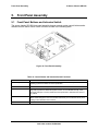
1.
SR1300 Feature Summary
SR1300 Feature Summary
The server chassis SR1300 is a 1U server chassis designed to support the Intel® server boards
SE7500WV2 and SR7501WV2. Both board and chassis have a feature set that is designed to
support the high-density server market. This specification details the specific feature set of the
Intel server chassis SR1300.
1.1
Chassis Views
Front view with bezel
Front view without bezel
Rear view
Figure 1. Front and Rear Chassis Views
Revision 1.2
1
Intel order number A94544-004
SR1300 Feature Summary
1.2
1U Server Chassis SR1300
Chassis Dimensions
Table 1. Chassis Dimensions
Height
43 mm
Width
430 mm
16.93 Inches
Depth
609.2 mm
23.89 Inches
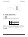
1.3
System Components
A
B
C
D
E
Power supply
PCI card bracket (full-length)
Riser card assembly
PCI card bracket (low-profile)
Server board (accessory to system)
F
G
Power distribution board
Air baffle
1.693 Inches
H
Fan module
I
Front panel board
J
Intrusion switch
K
Control panel
L
Flex bay, optional CD (or DVD) drive/FDD
module shown
M
Hard drive bay (one of two)
N
Backplane board
Figure 2. System Components
Revision 1.2
2
Intel order number A94544-004
1U Server Chassis SR1300
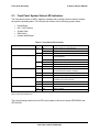
1.4
SR1300 Feature Summary
Chassis Back I/O Ports and Features
On the back of the chassis are cutouts for all external I/O connectors found on the server
boards SE7500WV2 and SE7501WV2. The I/O connector locations are pre-cut, so the use of
an I/O shield is not required.
A
B
C
D
E
F
PCI card bracket (low profile)
RJ45 NIC 2 connector
PCI card bracket (full-height)
Power supply
USB connector
RJ45 serial port
G
H
I
J
K
PS2 mouse/keyboard connector
RJ45 NIC 1 connector
SCSI connector (SCSI version only)
Video connector
USB connector
Figure 3. Chassis Back
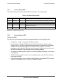
1.5
Chassis Front Panel and Peripheral Bays
Two external I/O connectors are located on the front panel assembly; one video connector and
one Universal Serial Bus (USB) connector.
A
B
C
D
E
F
Chassis handles (2)
Drive-type designator (If product is configured as ATA)
Drive bay (1-inch)
HDD activity/fault Indicator
Flex bay (optional CD[or DVD] drive/FDD module shown)
Front panel
Figure 4. Chassis Front
Revision 1.2
3
Intel order number A94544-004
SR1300 Feature Summary
1.5.1
1U Server Chassis SR1300
Front Panel Controls and Indicators
The front panel controls and indicators are shown below with an optional CDROM (or DVD)
drive/floppy disk drive installed.
M
N
O
P
Q
A
I
A
B
C
D
E
F
G
NIC 1 activity LED
NIC 2 activity LED
Power/sleep LED
Power button
System status LED
Fixed disk drive status LED
ID LED
H
ID button
I
Front Accessible Video (Switched video with
rear video connector)
B
C
D
J
E
F
K
G
H
L
J
NMI button (tool assisted)
K
USB Port
L
Reset button
M
Floppy activity LED
N
CDROM/DVD activity LED
O
CD-ROM drive eject button
P
Manual CD-ROM drive eject button (Tool
assisted)
Q
FDD eject button
Figure 5. Controls and Indicators
Revision 1.2
4
Intel order number A94544-004
1U Server Chassis SR1300
1.5.2
A
B
C
D
E
SR1300 Feature Summary
Peripheral Bays
Hard drive bays
Flex bay
Slimline CD-ROM drive/floppy or DVD/floppy drive module
Hard disk drive (Only in SCSI Backplane configuration)
Hard disk drive
Figure 6. Optional Peripherals
1.6
Power Supply
The power supply is rated for 350 watts of power at the following voltages:
•
•
90-132VAC (V) ∼ at 50/60 Hertz (Hz); 4.96 Ampere (A) maximum (max)
180-264VAC∼ at 50/60 Hz; 2.48 A maximum
The power subsystem supports implementation of remote management features, including
remote enable that permits power to be activated from a variety of sources.
1.7
System Cooling
The chassis includes a non-hot-swappable fan module with five fans for cooling the
processor(s), hard drives, and PCI cards. The fan pack is located in the middle of the chassis,
to pull cooling air through the chassis. The power supply contains two built-in fans for cooling.
Revision 1.2
5
Intel order number A94544-004
SR1300 Feature Summary
1.8
1U Server Chassis SR1300
Chassis Security
To help prevent unauthorized access to the system’s peripherals and control panel, an optional
key-locked front bezel can be used. The chassis also includes a preinstalled intrusion switch
that can be monitored by server management software. When the cover is opened, the switch,
located on the front panel board, transmits a signal to the Baseboard Management Controller
(BMC) on the server board. Through server management software, the system can be
programmed to respond to an intrusion by powering down or by locking the keyboard.
1.9
Rack and Cabinet Mounting Options
The server chassis SR1300 was designed to support 19” wide and up to 30” deep server
cabinets. The chassis comes equipped with a relay rack or cabinet mount kit that can be
configured to support front-mount or mid-mount 2-post racks and 4-post cabinets. Intel also
provides an optional sliding rail kit that is used to mount the chassis into a standard (19” x up to
30” deep) EIA-310D compatible server cabinet.
For mounting in a regular server cabinet, the front mount brackets are attached to the front of
the chassis, and a set of rear support brackets are attached to the back end of the cabinet. This
allows the weight of the server to be distributed evenly to prevent the mounting rails on the
cabinet from bending. Caution should be taken when selecting the 2-post, front-mount only
option. Even though the rail mount kit hardware was designed to support the weight of the
system, some 2-post relay racks may not support the weight, causing the racks to fail. Only use
relay racks that were specifically designed to support the weight and stresses of a 2-post, frontmount-only chassis.
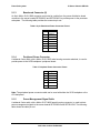
1.10 Front Bezel Features
The optional front bezel is made of molded plastic and uses a snap-on design. When installed,
its design allows for maximum airflow. Light pipes in the front bezel allow the system status
LEDs to be monitored with the bezel installed.
Figure 7. Optional Front Bezel
Revision 1.2
6
Intel order number A94544-004
1U Server Chassis SR1300
Power Sub-system
2.
Power Sub-system
2.1
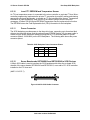
Power Distribution Board (PDB)
The server chassis SR1300 provides a power distribution board, eliminating the use of cables
for power distribution to various system components. The power distribution board provides
connectors to allow both the power supply and the baseboard to be plugged directly into it. In
addition, it provides a 6-pin power cable for power distribution to the multifunctional backplane
board, a 5-pin cable used to provide power management signals to the baseboard, and an 8-pin
(4-wire) connector to provide power to the baseboard for the processor subsystem.
Figure 8. Power Distribution Board Drawing
Revision 1.2
7
Intel order number A94544-004
Power Sub-system
2.1.1
1U Server Chassis SR1300
Power Supply Edge Connector Slot
An AMP* 1364999-1, or equivalent type of slot connector, is used to plug a blind mating edge
connector from the power supply. The following table provides the pin-out for the slot connector.
Table 2. Power Supply Edge Connector Slot Pinout
Pin
Signal
Description
Signal direction with respect to
connector on PDB
Input to PDB
B1
-12V
Voltage of 12V input from power supply
A1
PS_ON#
Logic signal to enable main power supply
outputs
Output from PDB
B2
PwrOk
Indicates that all outputs are within
regulation
Input to PDB
Bidirectional
A2
SDA
IPMB I2C Data
B3
Res
Reserved
A3
SCL
IPMB I2C Clock
Bidirectional
B4
AC Warn
Warning to system that power supply has
lost its AC input. No use.
Input to PDB
A4
PSAlert#
Indicates power supply is operating beyond
limits and has failed/may fail soon
Input to PDB
B5
5VSB
5V Stand-by voltage
Input to PDB
A5
ReturnS
Regulate out ground drops for all output
voltages
Output from PDB
B6
(Removed pin)
Keying pin. No connect
A6
Res
Reserved.
A7
Res
Reserved
B8
Res
Reserved
A8
3.3VS
Regulate out drops for in system for 3.3V
output
9
Res
Reserved
10
Res
Reserved
11
12V2
Input to PDB
12
12V2
Input to PDB
13
12V2
Input to PDB
14
12V1
Input to PDB
15
12V1
Input to PDB
16
12V1
17
Gnd
Ground
18
Gnd
Ground
19
Gnd
Ground
20
Gnd
Ground
21
Gnd
Ground
22
Gnd
Ground
23
Gnd
Ground
24
Gnd
Ground
Output from PDB
Input to PDB
Revision 1.2
8
Intel order number A94544-004
1U Server Chassis SR1300
Pin
Signal
Power Sub-system
Description
Signal direction with respect to
connector on PDB
25
Gnd
26
5V
Input to PDB
27
5V
Input to PDB
28
5V
Input to PDB
29
3.3V
Input to PDB
30
3.3V
Input to PDB
31
3.3V
Input to PDB
2.1.2
Ground
Baseboard Connector (1)
A 24-pin Molex* 15-24-7241 connector on the power distribution board allows for the server
boards SE7500WV2 and SE7501WV2 to be plugged directly into it. The following table
provides the connector pin-out.
Table 3. 24-pin Baseboard Power Connector Pinout
Pin
1
+3.3V
Signal
2
+3.3V
3
COMMON
4
+5V
5
COMMON
6
+5V
7
COMMON
8
PWR_OK
9
5VSB
10
+12V_IO
11
+12V_IO
12
+3.3V
13
+3.3V
14
–12V
15
COMMON
16
PS_ON#
17
COMMON
18
COMMON
19
COMMON
20
RESERVED_(-5V)
21
+5V
22
+5V
23
+5V
24
COMMON
Revision 1.2
9
Intel order number A94544-004
Power Sub-system
2.1.3
1U Server Chassis SR1300
Baseboard Connector (2)
An 8-pin Molex 39-01-2080 connector connected to a cable from the power distribution board
connects to the server boards SE7500WV2 and SE7501WV2 to provide power to the processor
subsystem. The following table provides the connector pin-out.
Table 4. 8-pin Baseboard Power Connector Pinout
2.1.4
Pin
1
Signal
Common
2
Common
3
NC
4
NC
5
+12V VRM
6
+12V VRM
7
NC
8
NC
Peripheral Power Connector
A soldered 6-wire cable, with a Molex 39-01-2065 male housing connector attached, is used to
provide power to the HDD backplane / peripheral board.
Table 5. Peripheral Power Connector Pinout
Pin
1
Signal
Common
2
Common
3
+5V
4
+12V
5
+12V
6
+3.3V
Note: The peripheral power connector cable can be used with either the SCSI backplane or the
ATA backplane.
2.1.5
Power Management Signal Cable
A soldered 5-wire cable, with a Molex 50-57-9405 female housing connector, is used to direct
power management signals to the server boards SE7500WV2 and SE7501WV2. The following
table shows the cable pin-out.
Revision 1.2
10
Intel order number A94544-004
1U Server Chassis SR1300
Power Sub-system
Table 6. Power Management Signal Cable Pinout
2.2
Pin
1
Signal
SMBus-SCL
Serial Clock
Description
2
SMBus-SDA
Serial Data. Information from the power supply
3
Reserved
Reserved
4
ReturnS
Return remote sense
5
3.3VS
3.3V sense
Power Supply
The server chassis SR1300 supports one 350W SSI EPS power supply.
The 350W power supply supports Power Factor Correction (PFC) and accepts AC input directly
from the power source. The power sub-system includes a remote enable feature, which permits
the power to be activated from a variety of sources, and allows the implementation of other
remote management features. Refer to the 350W SSI Power Supply Technical Product
Specification for additional details.
Figure 9. Power Supply Insertion
Revision 1.2
11
Intel order number A94544-004
Power Sub-system
1U Server Chassis SR1300
Table 7. Power Supply Input/Output Summary
Voltage
Current Rating
+3.3 VDC Output
16.0A Max
+5 VDC Output
12.0A Max
+12 V1DC Output
16.0A Max1 (18.0A peak2)
+12 V2DC Output
16.0A Max1 (18.0A peak2)
-12 VDC Output
0.5A
+5 VDC Standby
2.0A
Output balancing
Total combined output power of all output shall not exceed 350 W
AC Line Voltage
Auto-ranging for either 90-132 VAC or 180-264 VAC
AC Line Frequency
50/60 Hz
AC Input Current
4.96 Amp at 115 VAC. 2.48 Amp at 220 VAC
Notes:
1. Maximum continuous load on the combined 12V output shall not exceed 28A
2. Peak power and peak current loading shall be supported for a minimum of 12 seconds
2.2.1
Power Supply Mechanical Specifications
The approximate power supply dimensions are 40.0mm high X 106mm wide X 300.0mm deep.
The mechanical outline and dimensions are shown in the following figure.
Apparat en skall anslutas
till jordat uttag när den
ans luts till ett nätverk
Must connect to an earthed
mains s ock et-outlet
Figure 10. Outline Drawing Power System Enclosure 70-pin
Revision 1.2
12
Intel order number A94544-004
1U Server Chassis SR1300
Power Sub-system
The power supply has no power cable harness to distribute power to the system. Instead, the
power supply is plugged directly into a power distribution board by means of an edge connector.
The following table provides the pinout for the edge connector.
Table 8. Edge Connector Pinout
Description
Pin#
Pin#
Description
-12V
1
62
PSON#
PWOK
2
61
SDA
Reserved
3
60
SCL
Reserved
4
59
Reserved
5VSB
5
58
ReturnS
Removed keying pin
(NC)
6
57
Reserved
Reserved
7
56
Reserved
Reserved
8
55
3.3VS
Reserved
9
54
Reserved
Reserved
10
53
Reserved
12V2
11
52
12V2
12V2
12
51
12V2
12V2
13
50
12V2
12V1
14
49
12V1
12V1
15
48
12V1
12V1
16
47
12V1
Ground
17
46
Ground
Ground
18
45
Ground
Ground
19
44
Ground
Ground
20
43
Ground
Ground
21
42
Ground
Ground
22
41
Ground
Ground
23
40
Ground
Ground
24
39
Ground
Ground
25
38
Ground
5V
26
37
5V
5V
27
36
5V
Keying Position
5V
28
35
5V
3.3V
29
34
3.3V
3.3V
30
33
3.3V
3.3V
31
32
3.3V
Revision 1.2
13
Intel order number A94544-004
Power Sub-system
2.2.2
1U Server Chassis SR1300
Over Temperature Protection
The power supply will be protected against over temperature conditions caused by loss of fan
cooling or excessive ambient temperature. In an OTP condition the PSU will shutdown. When
the power supply temperature drops to within specified limits, the power supply shall restore
power automatically, while the 5V StandBy remains always on. The OTP circuit must have built
in hysteresis such that the power supply will not oscillate on and off due to temperature
recovering condition. The OTP trip level shall have a minimum of 4°C of ambient temperature
hysteresis.
2.2.3
Over Voltage Protection
The power supply Over Voltage Protection (OVP) is locally sensed. The power supply shall
shutdown and latch off after an over-voltage condition occurs. This latch shall be cleared by
toggling the PSON# signal or by an AC power interruption. The following table contains the
over-voltage limits. The values are measured at the output of the power supply’s connectors.
The voltage shall never exceed the maximum levels when measured at the power pins of the
power supply connector during any single point of fail. The voltage shall never trip any lower
than the minimum levels when measured at the power pins of the power supply connector.
Table 9. Over Voltage (OVP) Limits
Output Voltage
+3.3 V
2.2.4
MIN (V)
3.9
MAX (V)
4.5
+5 V
5.7
6.2
+12 V1,2
13.3
14.5
-12V
-13.3
-14.5
+5VSB
5.7
6.5
Power Supply LED Indicator
There will be a single GREEN LED to indicate power supply status. When AC is applied to the
PSU and standby voltages are available the LED shall BLINK GREEN. The LED shall turn ON
GREEN to indicate that all the power outputs are available. Refer to the table below for
conditions of the LED.
Table 10. LED Indicator Modes
Power Supply Condition
No AC power to PSU
Power Supply LED
OFF
AC present / Only Standby Outputs On
BLINK GREEN
Power supply DC outputs ON and OK
GREEN
Revision 1.2
14
Intel order number A94544-004
1U Server Chassis SR1300
3.
Chassis Cooling
Chassis Cooling
A five-fan module and the two power supply fans provide the necessary airflow to cool the
system. A fan on the processor heat sink is not necessary in this chassis.
Note: Certain processor kits may come with a Processor Wind Tunnel (PWT) cooling fan and
duct for each processor. This cannot be used in the server chassis SR1300 and is not
necessary.
In order to maintain the necessary airflow within the system, the air baffle must be installed
between the power supply and the fan module.
Figure 11. Air Baffle Installation
3.1
Five-Fan Module
A module consisting of five 40mm, multi-speed fans provides the primary airflow for the system.
A 12-wire cable/connector provides the fan module with power and tach lines, allowing each fan
to be monitored independently by server management software. The power cable is connected
to a 12-pin header located on the server boards SE7500WV2 and SE7501WV2. The following
table provides the pinout for the 12-wire cable/connector.
Revision 1.2
15
Intel order number A94544-004
Chassis Cooling
1U Server Chassis SR1300
Table 11. Fan Module Power Cable Pinout
Pin
1
Signal Name
Common
Type
Power
Description
Ground connection between fanboard and serverboard
2
Common
Power
Ground connection between fanboard and serverboard
3
Common
Power
Ground connection between fanboard and serverboard
4
PWM_Power
Power
Power connection between fanboard and serverboard
5
PWM_Power
Power
Power connection between fanboard and serverboard
6
PWM_Power
Power
Power connection between fanboard and serverboard
7
PWM_Power
Power
Power connection between fanboard and serverboard
8
Tach1
In
Tachometer for fan1 (innermost fan)
9
Tach2
In
Tachometer for fan2
10
Tach3
In
Tachometer for fan3
11
Tach4
In
Tachometer for fan4
12
Tach5
In
Tachometer for fan5 (outermost fan – close to wall of chassis)
Each fan within the module is capable of supporting multiple speeds. If the internal ambient
temperature of the system exceeds the value programmed into the thermal sensor data record
(SDR), the Baseboard Management Controller (BMC) firmware will increase the rotational
speed for all the fans within fan module.
The fan module is a single component. The individual fans that make up the module are not
swappable or individually replaceable. Should a fan fail, the entire module will need to be
replaced. A tab on the side of the fan module makes replacement of the module tool-less and
very simple. The fan module is not hot swappable. The server must be turned off before the fan
module can be replaced.
Figure 12. Fan Module Extraction
Revision 1.2
16
Intel order number A94544-004
1U Server Chassis SR1300
4.
Chassis Peripheral Bays
Chassis Peripheral Bays
The server chassis SR1300 provides two drive bays and one flex bay at the front of the chassis.
In SCSI configurations, all three drive bays may be populated with a tray-mounted 3.5” Single
Connector Attachment (SCA) SCSI hard disk drive. If a configuration requires the use of a
floppy disk drive and CDROM or DVDROM drive, an optional Floppy/CDROM or
Floppy/DVDROM module may be used in place of the third hard drive in the flex bay.
In ATA configurations, the chassis will support up to two tray-mounted 3.5” ATA drives in the
first two bays, and the optional Floppy/CDROM or Floppy/DVDROM module in the flex bay.
A
B
C
D
E
Hard drive bays
Flex bay
Slimline DVD/CD-ROM drive/FDD module
Hard disk drive (Only in SCSI Backplane configurations)
Hard disk drive
Figure 13. SR1300 Peripheral Bay Configuration Options
Revision 1.2
17
Intel order number A94544-004
Chassis Peripheral Bays
4.1
1U Server Chassis SR1300
Flex Bay Options
The third drive bay, or flex bay, is a multi-purpose drive bay. In SCSI configurations, the flex
bay may be used for either a third hot-swappable SCSI drive or an optional floppy/CDROM or
floppy/DVD module.
For ATA-100 configurations, the flex bay is only used to support these optional modules.
The Floppy/CDROM module is a 3.5” floppy drive and a 0.5” (12.7mm) slim line CD-ROM drive
mounted as a single unit in the flex bay. The Floppy/DVDROM module includes a DVDROM
instead of a CDROM drive. This module cannot be hot swapped. The system must be
powered down before the module can be inserted or removed.
Figure 14. Optional DVD/CD-ROM Drive / FDD Module
4.2
Hard Disk Drive Bays
Depending on which backplane is used, SCSI or ATA, the server chassis SR1300 can support
two or three hard disk drives.
For a SCSI configuration, the chassis will support up to three tray mounted SCA2, 3.5” x 1”,
Ultra2/Ultra160/Ultra 320 hard drives. With proper operating system (OS) or Redundant Array
of Inexpensive Drives (RAID) configuration, SCSI drives may be hot swapped while the system
is running.
For ATA configurations, the chassis will support up to two 3.5” x 1”, ATA-100 hard disk drives.
The third drive bay may be used for an optional floppy/CDROM or floppy/DVD module. ATA
hard drives cannot be hot swapped. Attempting to hot swap an ATA drive may cause
damage to the hard drive and/or cause loss of data.
Note: ATA drives from both Western Digital* and Maxtor* have been found to have their
interface connectors placed in a location that is mechanically not compatible for use with the
ATA backplane of the server chassis SR1300.
Revision 1.2
18
Intel order number A94544-004
1U Server Chassis SR1300
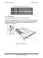
4.3
Chassis Peripheral Bays
Drive Trays
Each hard drive used in the system must be mounted to a drive tray, making insertion and
extraction of the drive from the chassis very simple. Each drive tray has its own dual purpose
latching mechanism which is used to both insert/extract drives from the chassis and lock the
tray in place. Each drive tray supports a light pipe providing a drive status indicator, located on
the backplane, to be viewable from the front of the chassis.
E
A
B
C
D
OM11684
A
B
C
D
E
Front of Drive
Front of Carrier
Drive Rail
Screw
SCA Connector
Figure 15. Drive Tray Assembly
Revision 1.2
19
Intel order number A94544-004
Front Panel Assembly
1U Server Chassis SR1300
5.
Front Panel Assembly
5.1
Front Panel Buttons and Intrusion Switch
The server chassis SR1300 front panel assembly houses several system control buttons and a
chassis intrusion switch. Each of their functions is listed in the following table.
Figure 16. Front Panel Assembly
Table 12. Control Button and Intrusion Switch Functions
Feature
Power/Sleep Button
Function
Toggles the system power on/off. This button is also used as a sleep button for
operating systems that follow the ACPI specification
Reset button
Reboots and initializes the system
NMI button
Pressing the recessed button with a paper clip or pin puts the server in a halt state for
diagnostic purposes and allows the system to issue a non-maskable interrupt. After
issuing the interrupt, a memory download can be performed to determine the cause of
the problem
ID button
Toggles the front panel ID LED and the baseboard ID LED on/off. The baseboard ID
LED is visible through the rear of the chassis and allows you to locate the server you’re
working on from behind a rack of servers
Chassis Intrusion Switch
A chassis intrusion switch is located on the front panel board
Revision 1.2
20
Intel order number A94544-004
1U Server Chassis SR1300
Front Panel Assembly
Figure 17. Front Panel Assembly Interface Board, Front View
5.2
Front Panel Assembly Connectors
The front panel assembly has two external I/O connectors:
•
•
One USB
One video
The following tables provide the pinouts for both types of connectors.
Table 13. External USB Connector
Pin #
1
I/O
USBPWR
Description
VREG_FP_USBPWR3
2
I/O
USB_DM3_FP
3
I/O
USB_DP3_FP
4
PWR
GND
The DB15 video connector located on the front panel is designed to access the video of the
system from the front panel of the system. Both the front and rear Video ports share the same
video signals. By default, the rear video port is enabled when there is no monitor connected to
the front video port. When a monitor is connected to the front video port, logic on the
baseboard will disable the rear video port and direct the video signal to the monitor connected
to the front panel.
Revision 1.2
21
Intel order number A94544-004
Front Panel Assembly
1U Server Chassis SR1300
Table 14. Video Connector
Pin #
1
I/O
O
Description
Red
2
O
Green
3
O
Blue
4
O
No Connect
5
Pwr
GND
6
Pwr
GND
7
I
Video Switch
8
Pwr
GND
Pwr
GND
9
10
No Connect
11
No Connect
12
No Connect
13
O
Hsync
14
O
Vsync
15
No Connect
If a monitor is connected to the front panel video connector, the rear video port (on the server
boards SE7500WV2 and SE7501WV2) will be disabled and the front panel video will be
enabled. The video source is the same for both connectors and is switched between the two,
with the front panel having priority over the rear video. This provides for easy front accessibility
to the server.
In addition, the front panel assembly interface board has two internal connectors:
•
A 34-pin header provides control and status information to/from the baseboard through
the HDD backplane board
•
A 10-pin USB header provides control for one USB port from the baseboard
A 34-pin flat cable is used to connect the front panel to the selected hard drive backplane. The
backplane provides a signal path to a 100-pin connector, which is then cabled to the server
boards SE7500WV2 and SE7501WV2.
Table 15. Internal USB Header
Pin #
1
I/O
PWR
Description
USB Power 3
2
PWR
USB Power 2
3
I/O
USB_P2_L
4
I/O
USB_P3_L
5
I/O
USB_P2
6
I/O
USB_P3
7
PWR
GND
8
PWR
GND
9
NC
NC
10
NC
NC
Revision 1.2
22
Intel order number A94544-004
1U Server Chassis SR1300
Front Panel Assembly
Table 16. Front Panel to HDD Backplane Connector
Pin #
1
I/O
NC
Description
ZZ_V_SWITCH_L
2
NC
TP_FP34_P33
3
I
GND
4
O
V_IO_RED_CONN_FP
5
PWR
GND
6
I
V_IO_GREEN_CONN_FP
7
PWR
GND
8
I
V_IO_BLUE_CONN_FP
9
I
V_IO_HSYNC_BUFF_FP_L
10
I
V_IO_VSYNC_BUFF_FP_L
11
O
NIC2_LED_ON_ACTIVITY
12
I
FP_NMI_BTN_L
13
NC
NC_FP_RSV2
14
NC
NC_FP_KEY
15
O
NIC2_LED_3V_LINK_L
16
PWR
GND
17
I
CHASSIS_INTRUSION_L
18
I
ID_SW_ACTIVE_L
19
I/O
I2C_CLK
20
O
CLIFTON/GIFFORD_LED_CATHOD_L
21
I/O
I2C_DATA
22
I
RST_SW_ACTIVE_L
23
O
NIC1_LED_ON_ACTIVITY
24
O
HDD_LED_FAULT_L
25
O
NIC1_LED_3V_LINK_L
26
I
PWR_SW_ACTIVE_L
27
O
ID_LED_ON_L
28
O
HDD_LED_ON_L
29
PWR
SB5V
30
PWR
VCC
31
O
FP_SYS_FLT_LED2_L
32
O
POWER_LED_ON_L
33
I
FP_SYS_FLT_LED1_L
34
I
LED Anode for another Model
Revision 1.2
23
Intel order number A94544-004
Front Panel Assembly
5.3
1U Server Chassis SR1300
Front Panel System Status LED Indicators
The front panel houses six LEDs, which are viewable with or without the front bezel to display
the system’s operating state. The LEDs provide a status for the following system states:
•
•
•
•
•
Power/Sleep
NIC1 / NIC2 Activity
System State
Disk Activity
System Identification
Table 17. Front Panel LED Functions
LED
Power/Sleep1
System Status on standby power
Fixed Disk Activity
Identify
NIC1 / NIC2 Activity Identify
Color
Green
State
Description
ON
Legacy Power On / ACPI S0 state
Blink
Sleep / ACPI S1 state
Off
OFF
Power Off / ACPI S4 or S5 state
Green
ON
Running. BIOS Initialization complete, boot started /
normal operation
Blink
Degraded condition
Amber
ON
Critical or Non-Recoverable condition
Blink
Non-Critical condition
Off
OFF
POST / System Stop
Green
Random blink
Hard disk activity. This is an ‘OR’ of the activity for
the onboard SCSI and IDE controllers
Amber
ON
Hard disk fault. Cleared when powered off
Off
OFF
No hard disk activity nor fault
Blue
ON
Identify Active via button. The button has
precedence over the command
Blue
Blink
Identify Active via command
Off
OFF
No Identification
Green
On
Link
Green
Blink
Network Activity
Note:
BIOS controls Power/Sleep LED
The current limiting resistors for the LED’s are located on the server boards SE7500WV2 and
SE7501WV2.
Revision 1.2
24
Intel order number A94544-004
1U Server Chassis SR1300
5.3.1
Front Panel Assembly
Power / Sleep LED
The BIOS controls the front panel Power LED as described in the following table.
Table 18. SSI Power LED Operation
State
Power Off
Power Mode
Non-ACPI
OFF
LED
Description
System power is off, and the BIOS has not initialized the chipset
Power On
Non-ACPI
ON
System power is on, but the BIOS has not yet initialized the chipset
S5
ACPI
OFF
Mechanical Off, and the OS has not saved any context to the hard disk
S4
ACPI
OFF
Mechanical Off. The OS has saved context to the hard disk
S3-S1
ACPI
Slow Blink 1
DC Power is still on. The OS has saved context and gone into some
level of low-power state
S0
ACPI
Steady On
System and the OS are up and running
Note:
Blink rate is ~1 Hz with at 50% duty cycle
5.3.2
System Status LED
Critical Condition
Any critical or non-recoverable threshold crossing associated with the following events:
•
Temperature, voltage, or fan critical threshold crossing
•
Power subsystem failure. The BMC asserts this failure whenever it detects a power
control fault (e.g., the BMC detects that the system power is remaining on even though
the BMC has deasserted the signal to turn off power to the system). A hot-swap
backplane would use the Set Fault Indication command to indicate when one or more of
the drive fault status LEDs are asserted on the hot-swap backplane
•
The system is unable to power up due to incorrectly installed processor(s), or processor
incompatibility
•
Satellite controller sends a critical or non-recoverable state, via the Set Fault Indication
command to the BMC
•
“Critical Event Logging” errors, including: System Memory Uncorrectable ECC error and
Fatal/Uncorrectable Bus errors, such as PCI SERR and PERR
Revision 1.2
25
Intel order number A94544-004
Front Panel Assembly
1U Server Chassis SR1300
Non-Critical Condition
•
•
•
•
Temperature, voltage, or fan non-critical threshold crossing
Chassis intrusion
Satellite controller sends a non-critical state, via the Set Fault Indication command, to
the BMC
Set Fault Indication command from system BIOS. The BIOS may use the Set Fault
Indication command to indicate additional, non-critical status such as system memory or
CPU configuration changes
Degraded Condition
•
•
5.3.3
One or more processors are disabled by Fault Resilient Boot (FRB) or BIOS
BIOS has disabled or mapped out some of the system memory
Drive Activity LED
The Drive Activity LED on the front panel is used to indicate drive activity for either the SCSI
drives (SCSI configured system) or the ATA drives (ATA configured system). The server
boards SE7500WV2 and SE7501WV2 also provides a header giving access to this LED for
add-in IDE or SCSI controllers.
5.3.4
System Identification LED
The blue System Identification LED is used to help identify a system for servicing when it is
installed within a high-density rack or cabinet that is populated with several other similar
systems. The System ID LED is illuminated when the system ID button, located on the front
panel, is pressed.
Revision 1.2
26
Intel order number A94544-004
1U Server Chassis SR1300
6.
Hot-Swap SCSI Backplane
Hot-Swap SCSI Backplane
The server chassis SR1300 can support a multifunctional SCSI backplane, supporting the
following features:
•
•
•
•
•
•
•
•
•
6.1
Three SCA2 compatible hot-swap SCSI connectors
Floppy/CDROM module interface connector
Support for the following SCSI bus specifications: Ultra-2, Ultra-160, and Ultra-320
Active SCSI termination (SPI-4 compatible)
Support for dual mode LVD operations
Per-drive power control, including automatic slot power down upon drive removal
SAF-TE 1.0-compliant enclosure management and monitoring functions
Drive Activity/Fault LEDs
A pathway for signals from the 100-pin floppy/front panel (FP)/IDE connector to the 60pin floppy/CDROM module connector in the flex bay
Hot-Swap SCSI Backplane Layout
The hot-swap SCSI backplane , resides in the drive bay of the server chassis SR1300. Drive
bays 1 and 2 each have a SCA2 type SCSI connector. The flex bay, (the third peripheral bay on
the right side on the front of the chassis) has two separate stacked connectors providing
support for either a third SCSI hard drive or an optional floppy/CDROM module. All three drive
bays have a Drive Activity/Fault LED. Additional connectors include a 100-pin floppy/FP/IDE
connector, which is cabled to the baseboard; a 34-pin connector, which is cabled to the front
panel; and a 6-pin power connector, which is connected to the power distribution board.
The following diagram shows the board layout of the backplane.
Figure 18. Hot-Swap SCSI Backplane Layout
Revision 1.2
27
Intel order number A94544-004
Hot-Swap SCSI Backplane
6.2
1U Server Chassis SR1300
SCSI Backplane Configuration Jumpers
The following table describes the settings and functionality of the jumper block used on the
SR1300 hot-swap SCSI backplane.
Table 19. Hot-Swap Backplane Configuration Jumpers
Option
Firmware Update
Location
J4
Description
Placing this jumper in the “FORCE UPDATE” position forces external
firmware update of the program code stored in Flash memory. Placing this
jumper in the “NORMAL OPERATION” position allows normal operation
Flash Boot Block Write
J4
This jumper allows the boot block of the program flash to be updated.
“NORMAL OPERTATION” (default) does not allow the boot block to be
written to. “WRITE” allows updating of the boot block
6.3
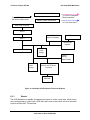
SCSI Backplane Functional Architecture
Functionality of the SCSI backplane begins at power-up. The microprocessor boots up via code
residing in the flash boot block. The SCSI backplane is capable of downloading firmware via
the IMB in-order to update the flash executable code.
The following figure shows the functional blocks of the hot-swap SCSI backplane.
Revision 1.2
28
Intel order number A94544-004
1U Server Chassis SR1300
Hot-Swap SCSI Backplane
CD-ROM & DVD /FDD
To FDD/CD Daughter
Board connector
From SE7500WV2 or
SE7501WV2 Base Board
FRONT PANEL INTERFACE
To Front Panel Board
Wide SCSI Connector
Drive 0
LVD/SE MultiMode Terminators
Drive 1
SE Terminator
53C80 SCSI
Interface
3860 LVD
to SE
Bridge
Drive 2
System
Memory
(RAM / ROM)
Drive
Power
Control
80C652 SAF-TE MicroController
Local I2C*
EEPROM
Figure 19. Hot-Swap SCSI Backplane Functional Diagram
6.3.1
Resets
The SCSI backplane is capable of supporting two types of resets; a cold reset, which occurs
when system power is cycled, and a SCSI bus reset, which occurs when the micro-controller
receives a Reset SAF-TE command.
Revision 1.2
29
Intel order number A94544-004
Hot-Swap SCSI Backplane
6.3.2
1U Server Chassis SR1300
Phillips* P80C652EBB Micro-Controller
The SCSI backplane supports the SAF-TE 1.0 specification and utilizes the Philips*
P80C652EBB micro-controller for all SAF-TE functions. If necessary, the backplane can
function without the SAF-TE micro-controller as a simple interconnection for the SCSI drives
and termination in LVD or single-ended (SE) mode.
P80C652XEBB features:
•
•
•
•
•
•
•
•
6.3.2.1
Operating frequency is 12 MHz
80C51-based architecture
Four 8-bit I/O ports
Two 16-bit timer/counters
Full-duplex Universal Asynchronous Receiver Transmitter (UART) facilities
I2C serial interface
Two power control modes - idle mode and power-down mode
Operating temperature range: 0°C to +70°C
I2C Serial Communication-SI01
The I2C pins are alternate functions to port pins P1.6 and P1.7. Because of this, P1.6 and P1.7,
on these parts, do not have a pull-up structure as found of the 80C51. Therefore P1.6 and P1.7
have open drain outputs on the 80C652.
6.3.2.2
I2C Electrical Input/Output Specifications
The I2C bus allows communication between devices made in different technologies, which might
also use different supply voltages.
For devices with fixed input levels, operating on a supply voltage of +5V ±10%, the following
levels have been defined:
•
•
VILmax = 1.5 V (maximum input low voltage)
VIHmin = 3 V (minimum input high voltage)
Devices operating on a fixed supply voltage different from +5 V (e.g., I2L), must also have these
input levels of 1.5 V and 3 V for VIL and VIH, respectively.
For devices operating over a wide rage of supply voltages (e.g.,Complementary Metal Oxide
Silicon {CMOS}), the following levels have been defined:
•
•
VILmax = 0.3 VDD (maximum input Low voltage)
VIHmin = 0.7 VDD (minimum input High voltage)
For both groups of devices, the maximum output low value has been defined:
•
VOLmax = 0.4 V (max. output voltage Low) at 3mA sink current
The maximum low-level input current at VOlmax, of both the SDA pin and the SCL pin of an I2C
device is, -10uA, including the leakage current of a possible output stage.
Revision 1.2
30
Intel order number A94544-004
1U Server Chassis SR1300
Hot-Swap SCSI Backplane
The maximum high-level input current at 0.9VDD, of both the SDA pin and SCL pin of an I2C
device, is 10uA, including the leakage current of a possible output stage.
The maximum capacitance, of both the SDA pin and the SCL pin of an I2C device, is 10pf.
6.3.2.3
•
•
Noise Margin
Noise margin minimum on the low level is 0.1 VDD.
Noise margin minimum on the high level is 0.2 VDD.
6.3.3
Symbios* SYM53C80S SCSI Controller
The SCSI backplane uses a Symbios SYM53C80S controller to perform all SCSI functions.
Device selection is memory mapped at address FB00-FC00. It is reset on power-up and, when
reset, is asserted to the backplane. SYM53C80S access slows down the bus; it is
recommended to pulse SAF-TE infrequently. SAF_TE command processing is 2-10ms.
The SYM53C80S supports the following features:
•
•
•
•
•
•
•
•
•
•
•
Supports the American National Standards Institute (ANSI) X3.131-1994 standard
Parity generation with optional checking
No external clock required
On-chip 48mA single-ended drivers and receivers
Functions in both the target and initiator roles
Direct control of all SCSI signals
Asynchronous data transfers of up to 5.0 Mbytes/second
Variety of packaging options
SCSI protocol efficiency is directly proportional to the speed of the microprocessor
CMOS parts provide additional grounding and controlled fall times that reduce noise
generated by SCSI bus switching
SCAM Level 1 and 2 compatibility
6.3.4
SCSI Interface
The SCSI interface on the SR1300 hot-swap SCSI backplane provides the required circuitry
between the SCSI bus and the 80C652 micro-controller. This allows the micro-controller to
respond as a SCSI target. The interface consists of a Symbios* 53C80S SCSI interface chip,
which functions as translator between the SCSI bus and the micro-controller. The 53C80S is a
single-ended, narrow device.
6.3.5
LVD to SE Bridge
Since the 53C80S is a single-ended, narrow device, an Adaptec* AIC-3860 LVD-to-SE
transceiver (bridge) is used to create a single-ended extension of the LVD bus. This allows the
53C80S to communicate with the LVD bus.
Revision 1.2
31
Intel order number A94544-004
Hot-Swap SCSI Backplane
6.3.6
1U Server Chassis SR1300
SCSI Termination
Passive SE termination is used for the single-ended extension of the SCSI bus on which the
53C80S resides.
LVD/SE multi-mode terminators provide SPI-4 compliant active termination for the backplane
end of the SCSI bus. It is assumed that the other end of the SCSI segment is properly
terminated as required by the SPI-4 specification. Multi-mode termination is implemented on the
SR1300 hot-swap SCSI backplane using two Unitrode* UCC5638 multi-mode SCSI 15-line
terminators.
6.3.7
Power Control
Power control on the SR1300 hot-swap SCSI backplane supports the following features:
•
Power-down of a drive when a failure is detected and reported (using enclosure services
messages) via the SCSI bus. This decreases the likelihood that the drive, which may be
under warranty, is damaged during removal from the hot-swap drive bay. When a new
drive is inserted, the power control waits a small amount of time for the drive to be fully
seated, and then applies power to the drive in preparation for operation.
•
If system power is on, the hot-swap SCSI backplane immediately powers off a drive slot
when it detects that a drive has been removed. This prevents possible damage to the
drive when it is partially removed and re-inserted while full power is available, and
disruption of the entire SCSI array from possible sags in supply voltage and resultant
current spikes.
•
Hot-spare drive support. Spare drives are kept in the hot-swap bay, but are left unpowered until a drive is determined to have failed. In this case, the hot spare can be
powered up and put into service automatically without requiring immediate operator
intervention to replace the drive.
•
The hot-swap SCSI backplane will automatically bypass the power control circuitry if a
shorted drive is inserted or if a drive develops a short during operation. This prevents
the hot-swap SCSI backplane from being damaged by a drive that draws excessive
current.
6.3.8
Drive Activity/Fault LEDs
Next to each hard drive connector is an Activity/Fault LED. The LEDs are activated by the
micro-controller and indicate either drive activity or a drive failure. The LEDs can be seen from
the front of the chassis by means of a light pipe mounted inside each hard drive carrier. During
initialization the micro-controller flashes the LEDs for one second as part of POST.
6.3.9
Internal Management Bus (IMB)
The IMB bus is a system-wide server management bus, based on the Phillips I2C bus
specification. It provides a way for various system components to communicate independently
with the standard system interfaces (e.g., PCI bus or processor/memory bus). The I2C bus
controller is integrated into the micro-controller. IMB connectivity is provided to the SCSI
backplane via the front panel connector.
Revision 1.2
32
Intel order number A94544-004
1U Server Chassis SR1300
6.3.10
Hot-Swap SCSI Backplane
Local I2C* EEPROM and Temperature Sensor
An I2C bus temperature sensor is connected to the micro-controller on a private I2C bus. Microcontroller programming implements the private I2C connection by explicitly setting and clearing
appropriate clock and data signals, to emulate an I2C-like interface to the sensor. Temperature
information is made available to other devices in the chassis using Enclosure Services
messages. A Dallas* DS1624 Serial EEPROM/Temperature Sensor implements this function.
The EEPROM stores the Field Replaceable Unit (FRU) information for the backplane.
6.3.11
Power Connector
The SCSI backplane provides power to the three drive bays, supporting up to three hard disk
drives or two hard disk drives, and the optional floppy/CDROM module. A 6-pin power cable is
routed from the power distribution board and plugs into a 2 x 3 shrouded plastic PC power
connector (Molex: 39-29-9066) on the SCSI backplane. The following table shows the power
connector pinout.
Table 20. SCSI Backplane Power Connector Pinout
6.3.12
Pin
1
Name
GND
Pin
4
Name
+12V
2
GND
5
+12V
3
+5V
6
Reserved
Server Baseboards SE7500WV2 and SE7501WV2 to SCSI Devices
A 68-pin SCSI cable is used to interface the SCSI backplane with either the on-board SCSI
channel of the server boards SE7500WV2 and SE7501WV2, or an add-in PCI SCSI controller
installed on the PCI riser card.
(AMP: 6-316173-7)
Figure 20. 68-Pin SCSI Cable Connector
Revision 1.2
33
Intel order number A94544-004
Hot-Swap SCSI Backplane
1U Server Chassis SR1300
Table 21. UltraWide (SE) and Ultra2 (LVD) SCSI Connector Pinout
6.3.13
Pin
1
Name
+DB (12)
Pin
18
Name
TERMPWR
Pin
35
Name
-DB (12)
Pin
52
Name
TERMPWR
2
+DB (13)
19
RESERVED
36
-DB (13)
53
RESERVED
3
+DB (14)
20
GROUND
37
-DB (14)
54
GROUND
4
+DB (15)
21
+ATN
38
-DB (15)
55
-ATN
5
+DB (P1)
22
GROUND
39
-DB (P1)
56
GROUND
6
+DB (0)
23
+BSY
40
-D B(0)
57
-BSY
7
+DB (1)
24
+ACK
41
-DB (1)
58
-ACK
8
+DB (2)
25
+RST
42
-DB (2)
59
-RST
9
+DB (3)
26
+MSG
43
-DB (3)
60
-MSG
10
+DB (4)
27
+SEL
44
-DB (4)
61
-SEL
11
+DB (5)
28
+C/D
45
-DB (5)
62
-C/D
12
+DB (6)
29
+REQ
46
-DB (6)
63
-REQ
13
+DB (7)
30
+I/O
47
-DB (7)
64
-I/O
14
+DB (P)
31
+DB (8)
48
-DB (P)
65
-DB (8)
15
GROUND
32
+DB (9)
49
GROUND
66
-DB (9)
16
DIFFSENS
33
+DB (10)
50
GROUND
67
-DB (10)
17
TERMPWR
34
+DB (11)
51
TERMPWR
68
-DB (11)
Server Baseboards SE7500WV2 and SE7501WV2 to CD(DVD)/FDD/FP
Interface
The SCSI backplane provides a pathway for the floppy/FP/IDE signals from the server
baseboardsSE7500WV2 and SE7501WV2 to the floppy/CDROM module interface board and
the front panel. The following table provides the pinout for the 100-pin (JAEE*: WR-100S-VF-1
or equivalent) connector.
Table 22. Floppy/FP/IDE Connector Pinout
Pin
A1
Name
GND
Pin
B1
Name
V_RED
A2
GND
B2
V_GREEN
A3
GND
B3
V_BLUE
A4
V_HSYNC_L
B4
V_VSYNC_L
A5
NIC2_LED_ON_ACTIVITY
B5
FP_NMI_BTN_L
A6
NIC2_LED_3V_LINK_L
B6
GND
A7
CHASSIS_INTRUSION
B7
ID_SW_ACTIVE_L
A8
I2C_CLK
B8
+5V STANDBY
A9
I2C_DATA
B9
RST_SW_ACTIVE_L
A10
NIC1_LED_ON_ACTIVITY
B10
HDD_LED_FAULT_L
A11
NIC1_LED_3V_LINK_L
B11
PWR_SW_ACTIVE_L
A12
ID_LED_ON_L
B12
HDD_LED_ON_L
A13
+5V STANDBY
B13
VCC
Revision 1.2
34
Intel order number A94544-004
1U Server Chassis SR1300
6.3.14
Hot-Swap SCSI Backplane
Pin
A14
Name
FP_SYS_FLT__LED2_L
Pin
B14
Name
POWER_LED_ON_L
A15
FP_SYS_FLT_LED1_L
B15
+5V STANDBY
A16
IPMB_5VSB_SCL
B16
RST_P6_PWR_GOOD
A17
GND
B17
IPMB_5VSB_SDA
A18
FDD_HDSEL_L
B18
GND
A19
GND
B19
FDD_DSKCHG_L
A20
FDD_RDATA_L
B20
FDD_WPROT_L
A21
GND
B21
FDD_TRK0_L
A22
FDD_WDATA_L
B22
GND
A23
GND
B23
FDD_WGATE_L
A24
FDD_STEP_L
B24
FDD_DIR_L
A25
GND
B25
FDD_DS0_L
A26
FDD_MTR0_L
B26
GND
A27
GND
B27
FDD_INDEX_L
A28
V_SWITCH_L
B28
GND
A29
GND
B29
FDD_DENSEL0
A30
CHP3_CDRST_L
B30
GND
A31
GND
B31
CDR_D7
A32
CDR_D8
B32
CDR_D6
A33
CDR_D9
B33
GND
A34
GND
B34
CDR_D5
A35
CDR_D10
B35
CDR_D4
A36
CDR_D11
B36
GND
A37
GND
B37
CDR_D3
A38
CDR_D12
B38
CDR_D2
A39
CDR_D13
B39
GND
A40
GND
B40
CDR_D1
A41
CDR_D14
B41
CDR_D0
A42
CDR_D15
B42
GND
A43
GND
B43
CDR_DREQ
A44
CDR_IOW_L
B44
GND
A45
CDR_IOR_L
B45
CDR_DACK_L
A46
CDR_IRDY
B46
GND
A47
CDR_IRQ
B47
CDR_ADDR1
A48
CDR_ADDR2
B48
CDR_ADDR0
A49
GND
B49
CDR_CS1_L
A50
CDR_CS3_L
B50
FDD/CDROM Daughter Board Connector
The SCSI backplane provides a pathway for floppy and IDE33 signals from the 100-pin
floppy/FP/IDE connector to the high density FDD/CDROM daughter board connector. See
Chapter 8 for additional details on the FDD/CDROM interface assembly.
Revision 1.2
35
Intel order number A94544-004
Hot-Swap SCSI Backplane
6.3.15
1U Server Chassis SR1300
Front Panel Interface Connector
The SCSI backplane provides a pathway for front panel signals from the 100-pin floppy/FP/IDE
connector to the FP connector (WY*:BHS-33A-2.0D-SM) . The pinout for the FP connector is
shown in the following table.
Table 23. SCSI Backplane FP Connector Pinout
Pin #
1
I
I/O
Description
LED Anode for another Model
2
I
FP_SYS_FLT_LED1_L
3
O
POWER_LED_ON_L
4
O
FP_SYS_FLT_LED2_L
5
PWR
VCC
6
PWR
SB5V
7
O
HDD_LED_ON_L
8
O
ID_LED_ON_L
9
I
PWR_SW_ACTIVE_L
10
O
NIC1_LED_3V_LINK_L
11
O
HDD_LED_FAULT_L
12
O
NIC1_LED_ON_ACTIVITY
13
I
RST_SW_ACTIVE_L
14
I/O
I2C_DATA
15
O
CLIFTON/GIFFORD_LED_CATHOD_L
16
I/O
I2C_CLK
17
I
ID_SW_ACTIVE_L
18
I
CHASSIS_INTRUSION_L
19
PWR
GND
20
O
NIC2_LED_3V_LINK_L
21
NC
NC_FP_KEY
22
NC
NC_FP_RSV2
23
I
FP_NMI_BTN_L
24
O
NIC2_LED_ON_ACTIVITY
25
I
V_IO_VSYNC_BUFF_FP_L
26
I
V_IO_HSYNC_BUFF_FP_L
27
I
V_IO_BLUE_CONN_FP
28
PWR
GND
29
I
V_IO_GREEN_CONN_FP
30
PWR
GND
31
O
V_IO_RED_CONN_FP
32
I
GND
33
NC
TP_FP34_P33
34
NC
ZZ_V_SWITCH_L
Revision 1.2
36
Intel order number A94544-004
1U Server Chassis SR1300
6.3.16
Hot-Swap SCSI Backplane
SCA2 Hot-Swap SCSI Drive Connectors
The SCSI backplane provides three hot-swap SCA2 connectors (Foxconn*: LS24403-J34) ,
which provide power and SCSI signals using a single connector. Each SCA drive attaches to
the backplane using one of these connectors.
Figure 21. 80-pin SCA2 SCSI Interface
Table 24. 80-pin SCA2 SCSI Interface Pinout
Pin
1
Signal Name
12V PreCharge
Signal Name
12V Ground
Pin
41
2
12V
12V Ground
42
3
12V
12V Ground
43
4
12V
Mated 1
44
5
3.3V
3.3V PreCharge
45
6
3.3V
DIFFSNS
46
7
-DB (11)
+DB (11)
47
8
-DB (10)
+DB (10)
48
9
-DB (9)
+DB (9)
49
10
-DB (8)
+DB (8)
50
11
-I/O
+I/O
51
12
-REQ
+REQ
52
13
-C/D
+C/D
53
14
-SEL
+SEL
54
15
-MSG
+MSG
55
16
-RST
+RST
56
17
-ACK
+ACK
57
18
-BSY
+BSY
58
19
-ATN
+ATN
59
20
-DB (P)
+DB (P)
60
21
-DB (7)
+DB (7)
61
22
-DB (6)
+DB (6)
62
23
-DB (5)
+DB (5)
63
24
-DB (4)
+DB (4)
64
25
-DB (3)
+DB (3)
65
26
-DB (2)
+DB (2)
66
27
-DB (1)
+DB (1)
67
28
-DB (0)
+DB (0)
68
Revision 1.2
37
Intel order number A94544-004
Hot-Swap SCSI Backplane
1U Server Chassis SR1300
Pin
29
Signal Name
-DB (P1)
Signal Name
+DB (P1)
Pin
69
30
-DB (15)
+DB (15)
70
31
-DB (14)
+DB (14)
71
32
-DB (13)
+DB (13)
72
33
-DB (12)
+DB (12)
73
34
5V
Mated 2
74
35
5V
5V Ground
75
36
5V PreCharge
5V Ground
76
37
Spindle Sync
Active LED Out
77
38
RMT_START
DLYD_START
78
39
SCSI ID (0)
SCSI ID (1)
79
40
SCSI ID (2)
SCSI ID (3)
80
Revision 1.2
38
Intel order number A94544-004
1U Server Chassis SR1300
7.
ATA Backplane
ATA Backplane
The server chassis SR1300 can support a multifunctional ATA backplane, supporting the
following features:
•
•
•
•
•
•
Two cold swappable ATA hard drive connectors
One floppy/CDROM or floppy/DVDROM module interface connector
Hard drive power-up control logic
Pathway for signals from the 100-pin floppy/FP/IDE connector to the 60-pin
floppy/CDROM and floppy/DVDROM module connector in the flex bay
Pathway for signals from the 100-pin floppy/FP/IDE connector to the front panel
connector
Drive Activity LEDs
Notes:
The ATA HDDI board does NOT support hot-swapping hard drives. Doing so may cause data
loss.
ATA drives from both Western Digital* and Maxtor* have been found to have their interface
connectors placed in a location that is mechanically not compatible for use with the ATA
backplane of the server chassis SR1300.
7.1
ATA Backplane Layout
The ATA backplane resides in the drive bay of the server chassis SR1300. Drive bays 1 and 2
each have a cold-swappable ATA drive connector and a 4-pin power connector. The flex bay,
(the third peripheral bay on the right side on the front of the chassis) has a raised connector
providing support for an optional Floppy/CDROM or Floppy/DVDROM module. Additional
connectors include a 100-pin floppy/FP/IDE connector, which is cabled to the baseboard; two
40-pin ATA 100 connectors, which are cabled to the baseboard; a 34-pin connector, which is
cabled to the front panel; and a 6-pin power connector, which is connected to the power jumper
board.
The following diagram shows the board layout of the backplane.
Revision 1.2
39
Intel order number A94544-004
ATA Backplane
1U Server Chassis SR1300
Figure 22. ATA Backplane Layout
7.2
ATA Backplane Functional Architecture
The ATA backplane is made up of the following functional blocks:
•
•
•
ATA100 bus with IDE connectors, which are combined with 4-pin power connectors
ATA drive power control
Peripheral/front panel interfaces
The figure below shows the functional blocks of the ATA backplane.
Revision 1.2
40
Intel order number A94544-004
1U Server Chassis SR1300
ATA Backplane
Figure 23. ATA Backplane Functional Block Diagram
7.2.1
Field Replaceable Unit (FRU)
The ATA backplane uses a Dallas* DS1624 to save board specific data, including serial
number. This is attached to the I2C bus of the front panel.
7.2.2
Power Control Logic and Driver
Although the ATA backplane does not support hot swapping of hard drives, the backplane
provides power control logic that reduces the chance of damage to a hard drive, should
someone attempt to remove or insert a drive while the system is powered on.
Only cold swapping of drives, (i.e., system must be powered off before the ATA drives or the
floppy/CDROM module can be inserted or extracted from the system) will be supported in the
server chassis SR1300.
7.2.3
Server Boards SE7500WV2 and SE7501WV2 to CD/FDD/FP Interface
The ATA backplane provides a pathway for signals from the 100-pin floppy/FP/IDE connector to
the high-density FDD/CD daughter board connector and the FP connector. The following table
provides the pinout for the 100-pin (JAEE*: WR-100S-VF-1) connector.
Revision 1.2
41
Intel order number A94544-004
ATA Backplane
1U Server Chassis SR1300
Table 25. Floppy/FP/IDE Connector Pinout
Pin
A1
GND
Name
Pin
B1
Name
V_IO_RED_CONN_FP_R
A2
GND
B2
V_IO_GREEN_CONN_FP_R
A3
GND
B3
V_IO_BLUE_CONN_FP_R
A4
V_IO_HSYNC_BUFF_FP_R_L
B4
V_IO_VSYNC_BUFF_FP_R
A5
NIC2_LED_ON_ACTIVITY
B5
FP_NMI_BTN_L
A6
NIC2_LED_3V_LINK_L
B6
GND
A7
CHASSIS_INTRUSION
B7
ID_SW_ACTIVE_L
A8
I2C_CLK
B8
+5V STANDBY
A9
I2C_DATA
B9
RST_SW_ACTIVE_L
A10
NIC1_LED_ON_ACTIVITY
B10
HDD_LED_FAULT_L
A11
NIC1_LED_3V_LINK_L
B11
PWR_SW_ACTIVE_L
A12
ID_LED_ON_L
B12
HDD_LED_ON_L
A13
+5V STANDBY
B13
+5V
A14
FP_SYS_FLT__LED2_L
B14
POWER_LED_ON_L
A15
FP_SYS_FLT_LED1_L
B15
+5V STANDBY
A16
IPMB_5VSB_SCL
B16
RST_P6_PWR_GOOD
A17
GND
B17
IPMB_5VSB_SDA
A18
FDD_HDSEL_L
B18
GND
A19
GND
B19
FDD_DSKCHG_L
A20
FDD_RDATA_L
B20
FDD_WPROT_L
A21
GND
B21
FDD_TRK0_L
A22
FDD_WDATA_L
B22
GND
A23
GND
B23
FDD_WGATE_L
A24
FDD_STEP_L
B24
FDD_DIR_L
A25
GND
B25
FDD_DS0_L
A26
FDD_MTR0_L
B26
GND
A27
GND
B27
FDD_INDEX_L
A28
V_SWITCH_L
B28
GND
A29
GND
B29
FDD_DENSEL0
A30
CHP3_CDRST_L
B30
GND
A31
GND
B31
CDR_D7
A32
CDR_D8
B32
CDR_D6
A33
CDR_D9
B33
GND
A34
GND
B34
CDR_D5
A35
CDR_D10
B35
CDR_D4
A36
CDR_D11
B36
GND
A37
GND
B37
CDR_D3
A38
CDR_D12
B38
CDR_D2
A39
CDR_D13
B39
GND
A40
GND
B40
CDR_D1
A41
CDR_D14
B41
CDR_D0
A42
CDR_D15
B42
GND
Revision 1.2
42
Intel order number A94544-004
1U Server Chassis SR1300
7.2.4
ATA Backplane
Pin
A43
GND
Name
Pin
B43
Name
CDR_DREQ
A44
CDR_IOW_L
B44
GND
A45
CDR_IOR_L
B45
CDR_DACK_L
A46
CDR_IRDY
B46
GND
A47
CDR_IRQ
B47
CDR_ADDR1
A48
CDR_ADDR2
B48
CDR_ADDR0
A49
GND
B49
CDR_CS1_L
A50
CDR_CS3_L
B50
FDD/CD Daughter Board Connector
The ATA backplane provides a pathway for floppy and IDE33 signals from the 100-pin
floppy/FP/IDE connector to the high-density FDD/CDROM daughter board connector. See
Chapter 8 for additional details on the FDD/CDROM interface assembly.
7.2.5
Front Panel Interface Connector
The ATA backplane provides a pathway for front panel signals from the 100-pin floppy/FP/IDE
connector to the front panel (FP) connector. The pinout for the FP (WY*:BHS-33A-2.0D-SM)
connector is shown in the following table.
Table 26. ATA Backplane FP Connector Pinout
Pin #
1
I
I/O
Description
LED Anode for another model
2
I
FP_SYS_FLT_LED1_L
3
O
POWER_LED_ON_L
4
O
FP_SYS_FLT_LED2_L
5
PWR
VCC
6
PWR
SB5V
7
O
HDD_LED_ON_L
8
O
ID_LED_ON_L
9
I
PWR_SW_ACTIVE_L
10
O
NIC1_LED_3V_LINK_L
11
O
HDD_LED_FAULT_L
12
O
NIC1_LED_ON_ACTIVITY
13
I
RST_SW_ACTIVE_L
14
I/O
I2C_DATA
15
O
CLIFTON/GIFFORD_LED_CATHOD_L
16
I/O
I2C_CLK
17
I
ID_SW_ACTIVE_L
18
I
CHASSIS_INTRUSION_L
19
PWR
GND
20
O
NIC2_LED_3V_LINK_L
21
NC
NC_FP_KEY
Revision 1.2
43
Intel order number A94544-004
ATA Backplane
7.2.6
1U Server Chassis SR1300
Pin #
22
I/O
NC
Description
NC_FP_RSV2
23
I
FP_NMI_BTN_L
24
O
NIC2_LED_ON_ACTIVITY
25
I
V_IO_VSYNC_BUFF_FP_L
26
I
V_IO_HSYNC_BUFF_FP_L
27
I
V_IO_BLUE_CONN_FP
28
PWR
GND
29
I
V_IO_GREEN_CONN_FP
30
PWR
GND
31
O
V_IO_RED_CONN_FP
32
I
GND
33
NC
TP_FP34_P33
34
NC
ZZ_V_SWITCH_L
ATA100 Connectors
The ATA backplane has two 40-pin ATA100 connectors. These connectors relay ATA100
signals from the baseboard to the ATA drives. Each connector is used for a separate ATA
channel. Each channel is configured as a bus master. The following table provides the pinout
for both 40-pin ATA100 connectors.
Table 27. 40-Pin ATA 100 Connector Pinout
Pin
1
Name
RESET_L
Pin
21
Name
IDEDRQ
2
GND
22
GND
3
DD7
23
DIOW_L
4
DD8
24
GND
5
DD6
25
DIOR_L
6
DD9
26
GND
7
DD5
27
IORDY
8
DD10
28
CSEL
9
DD4
29
IDEDAK_L
10
DD11
30
GND
11
DD3
31
IDEIRQ
12
DD12
32
Reserved (nc)
13
DD2
33
IDESA1
14
DD13
34
PDIAG_L
15
DD1
35
IDESA0
16
DD14
36
IDESA2
17
DD0
37
IDECS1_L
18
DD15
38
IDECS3_L
19
GND
39
IDEHDACT_L
20
Keyed
40
GND
Revision 1.2
44
Intel order number A94544-004
1U Server Chassis SR1300
7.2.7
ATA Backplane
Power Connector
The ATA backplane provides power for up to two ATA drives and one floppy/CD-ROM module.
A 6-line power cable is routed from the power distribution board and plugs into a connector on
the backplane.
Table 28. 6-Pin ATA Backplane Power Connector Pinout
7.2.8
Pin
1
Name
GND
Pin
4
Name
+12V
2
GND
5
+12V
3
+5V
6
Reserved
ATA100 Interface to Drive
The ATA drive interface combines both ATA and power signals into a single connector. The
pinout of the drive interface connector is the same as a standard ATA and power connector.
Revision 1.2
45
Intel order number A94544-004
Floppy/CDROM and Floppy/DVDROM Module Interface Assemblies
8.
1U Server Chassis SR1300
Floppy/CDROM and Floppy/DVDROM Module
Interface Assemblies
Two modules are available for use in the server chassis SR1300. Both support a floppy disk
drive, while one contains a CDROM drive and the other a DVDROM drive. The interface
assembly will be referred to as FDD/CDROM (though it supports DVDROM drives also).
The FDD/CDROM interface assembly consists of two pieces: a 60-pin high-density connector
located on both the SCSI and ATA backplanes, and a raised FDD/CD daughter board.
In the SCSI configuration, this assembly allows the daughter board to sit directly over the third
SCA2 SCSI connector, allowing for either a third SCSI hard drive or a floppy/CDROM or
floppy/DVD module to be used in the flex bay.
Both the SCSI and ATA backplanes provide a pathway for FDD/CD signals from the 100-pin
floppy/FP/IDE connector to the high-density 60-pin (Molex: 52760-0608) daughter board
connector. The following table provides the connector pinout.
Table 29. 60-Pin Daughter Card Connector Pinout
Pin
1
CDR_D1
Name
Pin
2
Name
CDR_D0
3
CDR_D13
4
CDR_D14
5
CDR_D2
6
CDR_D15
7
CDR_D12
8
CDR_IOW_L
9
CDR_D3
10
CDR_IOR_L
11
CDR_D11
12
CDR_IRDY
13
CDR_D4
14
CDR_IRQ
15
CDR_D10
16
CDR_ADDR1
17
CDR_D5
18
CDR_DACK_L
19
CDR_D9
20
CDR_ADDR0
21
CDR_D6
22
CDR_ADDR2
23
CDR_D8
24
CDR_CS1_L
25
CDR_D7
26
CDR_CS3_L
27
CHP3_CDRST_L
28
CDR_DREQ
29
GND
30
GND
31
GND
32
GND
33
GND
34
GND
*35
PWRCNTR1_FOR_IDE_HSBP
36
GND
*37
PWRCNTR2_FOR_IDE_HSBP
38
CD_FDD_PRSN_L
39
ACTIVE_L
40
FDD_HDSEL_L
41
FDD_INDEX_L
42
FDD_WPROT_L
43
FDD_DSKCHG_L
44
FDD_WGATE_L
45
FDD_DIR_L
46
FDD_STEP_L
47
FDD_WDATA_L
48
FDD_MTR0_L
Revision 1.2
46
Intel order number A94544-004
1U Server Chassis SR1300
Floppy/CDROM and Floppy/DVDROM Module Interface Assemblies
Pin
49
Name
FDD_DENSEL0
Pin
50
Name
FDD_DS0_L
51
FDD_TRK0_L
52
FDD_RDATA_L
53
VCC**
54
VCC**
55
VCC**
56
VCC**
57
VCC**
58
VCC**
59
VCC**
60
VCC**
Notes:
* This signal is used only on the ATA backplane.
** VCC means +5 V
The floppy/CDROM daughter board has two connectors, one on the bottom side of the board
which mates with the high density connector on the backplane, and an 80-pin SCA type
interface connector on the top side of the board, which is used as the interface for the
floppy/CDROM drive module.
Figure 24. Floppy/CDROM Daughter Board
The following table provides the pinout for the 80-pin (Molex:71661-2380) SCA connector.
Table 30. 80-Pin SCA Interface Pinout
1
Pin
NC
Signal Name
GND
Signal Name
Pin
41
2
NC
GND
42
3
NC
GND
43
4
NC
GND (DRIVE PSESENT SIGNAL ON)
44
5
NC
CDR_DREQ
45
6
NC
NC
46
7
CDR_CD3_L
CDR_CS1_L
47
8
CDR_ADDR2
CDR_ADDR0
48
9
CDR_DACK_L
CDR_ADDR1
49
10
CDR_IRQ
CDR_IRDY
50
11
CDR_IOR_L
CDR_IOW_L
51
Revision 1.2
47
Intel order number A94544-004
Floppy/CDROM and Floppy/DVDROM Module Interface Assemblies
Pin
1U Server Chassis SR1300
12
Signal Name
CDR_D (15)
CDR_D (0)
Signal Name
Pin
52
13
CDR_D (14)
CDR_D (1)
53
14
CDR_D (13)
CDR_D (2)
54
15
CDR_D (12)
CDR_D (3)
55
16
CDR_D (11)
CDR_D (4)
56
17
CDR_D (10)
CDR_D (5)
57
18
CDR_D (9)
CDR_D (6)
58
19
CDR_D (8)
CDR_D (7)
59
20
CHP3_CDRST_L
FDD_INDEX_L
60
21
FDD_DSKCHG_L
FDD_DIR_L
61
22
FDD_WDATA_L
FDD_DENSEL0
62
23
FDD_TRK0_L
FDD_DS0_L
63
24
FDD_RDATA_L
FDD_MTR0_L
64
25
FDD_STEP_L
FDD_WGATE_L
65
26
FDD_WPROT_L
FDD_HDSEL_L
66
27
PWRCNTR1_FOR_IDE HSBP
NC
67
28
PWRCNTR2_FOR_IDE HSBP
NC
68
29
NC
NC
69
30
NC
NC
70
31
NC
NC
71
32
NC
NC
72
33
NC
NC
73
34
VCC
GND
(DRIVE PSESENT SIGNAL ON)
74
35
VCC
GND
75
35
VCC
GND
75
36
VCC
GND
76
37
NC
10K Pull-up
(Disable DISK ACT LED)
77
38
NC
NC
78
39
NC
NC
79
40
NC
CD/FDD Enable (GND)
80
Revision 1.2
48
Intel order number A94544-004
1U Server Chassis SR1300
9.
PCI Riser Cards
PCI Riser Cards
The SR1300 1U server chassis supports the use of two single-slot PCI riser cards.
Each riser card is capable of supporting a 3.3 V, 64-bit add-in card. For the SCSI SKU, the
board supports 66 MHZ PCI in the low profile slot and up to 100MHZ PCI-X in the full height
slot. If the onboard 7899 SCSI device is disabled in BIOS setup, the low profile slot can support
100Mhz PCI-X. For the ATA SKU both low profile and full height slots support 100MHZ PCI-X.
Table 31. Max Conditions for PCI Riser Cards
Bus B with Anvik
Dual NIC down and 1
Slot Riser
Bus C with AIC7899
SCSI down and 1 Slot
Riser
Bus C with AIC7902
SCSI down and 1 Slot
Riser
0 Adapter Cards installed
and on board device
enabled
PCI-X 64/100
PCI-X 64/66
PCI-X 64/100
1 Adapter Cards installed
and on board device
enabled
PCI-X 64/100
PCI-X 64/66
PCI-X 64/100
Configuration
Figure 25. PCI Riser Card Diagram
Revision 1.2
49
Intel order number A94544-004
PCI Riser Cards
1U Server Chassis SR1300
The PCI riser card in the riser slot located closest to the edge of the baseboard will only support
low profile add-in cards. The second riser card is capable of supporting both full-height/fulllength and low-profile PCI cards (low profile PCI cards in this slot require full height PCI
brackets).
Figure 26. PCI Riser Assembly Diagram
The following table provides the pinout of the 64-bit PCI connector.
Table 32. 3-Volt 64-Bit PCI Connector Pinout
Pin
1
-12V
Side B
TRST#
Side A
Pin
49
Side B
M66EN
Side A
AD [09]
2
TCK
+12V
50
Ground
Ground
3
Ground
TMS
51
Ground
Ground
4
TDO
TDI
52
AD [08]
C/BE [0]#
5
+5V
+5V
53
AD [07]
+3.3V
6
+5V
INTA#
54
+3.3V
AD [06]
7
INTB#
INTC#
55
AD [05]
AD [04]
8
INTD#
+5V
56
AD [03]
Ground
9
PRSNT1#
Reserved
57
Ground
AD [02]
10
Reserved
+3.3V (I/O)
58
AD [01]
AD [00]
11
PRSNT2#
Reserved
59
+3.3V (I/O)
+3.3V (I/O)
12
CONNECTOR KEY
CONNECTOR KEY
60
ACK64#
REQ64#
13
CONNECTOR KEY
CONNECTOR KEY
61
+5V
+5V
14
Reserved
Reserved
62
+5V
+5V
Revision 1.2
50
Intel order number A94544-004
1U Server Chassis SR1300
PCI Riser Cards
Pin
15
Side B
Ground
RST#
Side A
Pin
Side B
CONNECTOR KEY
Side A
CONNECTOR KEY
16
CLK
+3.3V (I/O)
CONNECTOR KEY
CONNECTOR KEY
17
Ground
GNT#
63
Reserved
Ground
18
REQ#
Ground
64
Ground
C/BE [7]#
19
+3.3V (I/O)
Reserved
65
C/BE [6]#
C/BE [5]#
20
AD [31]
AD [30]
66
C/BE [4]#
+3.3V (I/O)
21
AD [29]
+3.3V
67
Ground
PAR64
22
Ground
AD [28]
68
AD [63]
AD [62]
23
AD [27]
AD [26]
69
AD [61]
Ground
24
AD [25]
Ground
70
+3.3V (I/O)
AD [60]
25
+3.3V
AD [24]
71
AD [59]
AD [58]
26
C/BE [3]#
IDLES
72
AD [57]
Ground
27
AD [23]
+3.3V
73
Ground
AD [56]
28
Ground
AD [22]
74
AD [55]
AD [54]
29
AD [21]
AD [20]
75
AD [53]
+3.3V (I/O)
30
AD [19]
Ground
76
Ground
AD [52]
31
+3.3V
AD [18]
77
AD [51]
AD [50]
32
AD [17]
AD [16]
78
AD [49]
Ground
33
C/BE [2]#
+3.3V
79
+3.3V (I/O)
AD [48]
34
Ground
FRAME#
80
AD [47]
AD [46]
35
IRDY#
Ground
81
AD [45]
Ground
36
+3.3V
TRDY#
82
Ground
AD [44]
37
DEVSEL#
Ground
83
AD [43]
AD [42]
38
Ground
STOP#
84
AD [41]
+3.3V (I/O)
39
LOCK#
+3.3V
85
Ground
AD [40]
40
PERR#
SDONE
86
AD [39]
AD [38]
41
+3.3V
SBO#
87
AD [37]
Ground
42
SERR#
Ground
88
+3.3V (I/O)
AD [36]
43
+3.3V
PAR
89
AD [35]
AD [34]
44
C/BE [1]#
AD [15]
90
AD [33]
Ground
45
AD [14]
+3.3V
91
Ground
AD [32]
46
Ground
AD [13]
92
Reserved
Reserved
47
AD [12]
AD [11]
93
Reserved
Ground
48
AD [10]
Ground
94
Ground
Reserved
Revision 1.2
51
Intel order number A94544-004
PCI Riser Cards
1U Server Chassis SR1300
Figure 27. 1U PCI Riser Card Mechanical Drawing
Revision 1.2
52
Intel order number A94544-004
1U Server Chassis SR1300
Supported Intel® Server Boards
10. Supported Intel® Server Boards
The SR1300 1U server chassis is designed to support the feature requirements of the Intel®
server boards SE7500WV2 and SE7501WV2. Please refer to the SE7500WV2 Technical
Product Specification and the SE7501WV2 Technical Product Specification for additional
baseboard information.
Two server boards SE7500WV2 and two server boards SE7501WV2 will be made available.
One of the sever board SE7500WV2 will provide an embedded Ultra-160 SCSI interface, and
the other SE7500WV2 board will provide an embedded ATA-100 “Valu-Raid” interface. One of
the server board SE7501WV2 will provide an embedded Ultra-320 SCSI interface, and the other
SE7501WV2 board will provide an embedded ATA-100 “Valu-Raid” interface. Both boards will
support the following feature set:
•
•
•
•
•
•
•
Dual Intel® Xeon™ processors socket 604
Intel® E7500 chipset or E7501 chipset
Support for six DDR 200/266 Registered ECC memory with two-way interleaving up to 12 GBs
Notes:
Only low profile DIMMs are supported in the SR1300 server chassis.
2 GB DIMM thermal performance is unproven
The server board SE7501WV2 only supports DDR266 memory modules when using
533MHz processors
Three separate PCI buses:
- Segment A: 32-bit, 33 MHz, 5 V (P32-A) with four embedded devices:
• 2D/3D graphics controller: ATI RAGE* XL video controller with 8 MB of SDRAM
• ATA-100 controller: Promise Technology* PDC20277 (ATA-100 SE7500WV2
and SE7501WV2 server board only)
- Segment B: 64-bit, up to 100MHz PCI-X (66Mhz PCI for SCSI server board
SE7500WV2), 3.3 V, (P64-B) supporting the following configuration:
• One PCI I/O riser slot capable of supporting full length PCI add-in cards
• Two network interface controllers: Intel® 82546PM Fast Ethernet Controllers
- Segment C: 64-bit, up to 100MHz, 3.3 V (P64-C) supporting the following devices:
• One PCI I/O riser slot, with support for low-profile PCI add-in cards only
• Dual-channel wide Ultra-160 SCSI controller on the server board SE7500WV2
and Ultra- 320 SCSI controller on the server board SE7501WV2 providing one
internal and one high density external channel support: Adaptec* AIC-7899W
SCSI Controller (SCSI server board SE7500WV2 only) or Adaptec* AIC-7902
SCSI Controller (SCSI server board SE7501WV2 only).
LPC (Low Pin Count) bus segment with two embedded devices:
- Platform Management Controller (PMC) providing monitoring, alerting, and logging of
critical system information obtained from embedded sensors on server board
- Super I/O controller chip providing all PC-compatible I/O (floppy, serial, keyboard, mouse)
X-Bus segment with one embedded device:
- Flash ROM device for system BIOS: Intel® 32-megabit 28F320C3 Flash ROM
Revision 1.2
53
Intel order number A94544-004
Serial Port Usage
•
•
•
•
•
1U Server Chassis SR1300
Two external Universal Serial Bus (USB) ports on the rear of the board with an additional
internal header that provides one optional USB port for front panel support
One external low-profile RJ45 Serial B port on the back of the board.
Support for up to 5 multi-speed fans (via single 12pin fan header) and 2 fixed speed fans
SSI compliant connectors for SSI interface support.
Multifunctional high-density connector for use in server chassis SR1300: front panel,
floppy, and IDE.
11. Serial Port Usage
The SR1300 server chassis, when integrated with a server board SE7500WV2 or SE7501WV2,
provides one external RJ45 serial port (Serial B) .
The use of RJ45 connectors for the serial interface is widely becoming a standard for use in the
high-density server market. The intended usage model for the RJ45 serial connector is for use
as an interface to a serial port concentrator allowing for remote access to the server’s
Emergency Management Port (EMP). See the SE7500WV2 or SE7501WV2 Hardware
Technical Product Specifications for more information concerning server management and EMP
usage.
The intended use for the RJ45 serial port, located in the back of the system, is for remote EMP
communication by connecting the port to a serial terminal concentrator. With the optional RJ45to-DB9 adapter, the serial port can also be configured for use with a modem or other serial
device requiring a DB9 connection to the serial port.
Revision 1.2
54
Intel order number A94544-004
1U Server Chassis SR1300
Regulatory and Integration Information
12. Regulatory and Integration Information
12.1 Product Regulatory Compliance
12.1.1
Product Safety Compliance
The server board SE7500WV2 and SE7501WV2 complies with the following safety
requirements:
•
•
•
•
•
UL 1950 - CSA 950 (US/Canada)
EN 60 950 (European Union)
IEC60 950 (International)
CE – Low Voltage Directive (73/23/EEC) (European Union)
EMKO-TSE (74-SEC) 207/94 (Nordics)
12.1.2
Product EMC Compliance
The server boards SE7500WV2 and SE7501WV2 have tested and verified to comply with the
following electromagnetic compatibility (EMC) regulations when installed a compatible Intel host
system. For information on compatible host system(s) refer to Intel’s Server Builder website or
contact your local Intel representative.
•
•
•
•
•
•
•
•
•
•
•
FCC (Class A Verification) – Radiated & Conducted Emissions (USA)
ICES-003 (Class A) – Radiated & Conducted Emissions (Canada)
CISPR 22 (Class A) – Radiated & Conducted Emissions (International)
EN55022 (Class A) – Radiated & Conducted Emissions (European Union)
EN55024 (Immunity) (European Union)
EN61000-3-2 & -3 (Power Harmonics & Fluctuation and Flicker)
CE – EMC Directive (89/336/EEC) (European Union)
VCCI (Class A) – Radiated & Conducted Emissions (Japan)
AS/NZS 3548 (Class A) – Radiated & Conducted Emissions (Australia / New Zealand)
RRL (Class A) Radiated & Conducted Emissions (Korea)
BSMI (Class A) Radiated & Conducted Emissions (Taiwan)
Revision 1.2
55
Intel order number A94544-004
Regulatory and Integration Information
12.1.3
1U Server Chassis SR1300
Product Regulatory Compliance Markings
This product is provided with the following Product Certification Markings.
•
•
•
•
•
•
•
•
•
UL / cUL Listing Mark
CE Mark
German GS Mark
Russian GOST Mark
FCC, Class A Verification Marking
ICES-003 (Canada EMC Compliance Marking)
VCCI, Class A Mark
Australian C-Tick Mark
Taiwan BSMI Certification Number and Class A Warning
12.2 Electromagnetic Compatibility Notices
12.2.1
USA
This device complies with Part 15 of the FCC Rules. Operation is subject to the following two
conditions: (1) this device may not cause harmful interference, and (2) this device must accept
any interference received, including interference that may cause undesired operation.
For questions related to the EMC performance of this product, contact:
Intel Corporation
5200 N.E. Elam Young Parkway
Hillsboro, OR 97124
1-800-628-8686
This equipment has been tested and found to comply with the limits for a Class A digital device,
pursuant to Part 15 of the FCC Rules. These limits are designed to provide reasonable
protection against harmful interference in a residential installation. This equipment generates,
uses, and can radiate radio frequency energy and, if not installed and used in accordance with
the instructions, may cause harmful interference to radio communications. However, there is no
guarantee that interference will not occur in a particular installation. If this equipment does
cause harmful interference to radio or television reception, which can be determined by turning
the equipment off and on, the user is encouraged to try to correct the interference by one or
more of the following measures:
•
•
•
•
Reorient or relocate the receiving antenna
Increase the separation between the equipment and the receiver
Connect the equipment to an outlet on a circuit other than the one to which the receiver
is connected
Consult the dealer or an experienced radio/TV technician for help
Any changes or modifications not expressly approved by the grantee of this device could void
the user’s authority to operate the equipment. The customer is responsible for ensuring
compliance of the modified product.
Revision 1.2
56
Intel order number A94544-004
1U Server Chassis SR1300
Regulatory and Integration Information
Only peripherals (computer input/output devices, terminals, printers, etc.) that comply with FCC
Class B limits may be attached to this computer product. Operation with noncompliant
peripherals is likely to result in interference to radio and TV reception.
All cables used to connect to peripherals must be shielded and grounded. Operation with
cables, connected to peripherals, that are not shielded and grounded may result in interference
to radio and TV reception.
12.2.2
FCC Verification Statement
Product Type: SR1300
This device complies with Part 15 of the FCC Rules. Operation is subject to the following two
conditions: (1) This device may not cause harmful interference, and (2) this device must accept
any interference received, including interference that may cause undesired operation.
For questions related to the EMC performance of this product, contact:
Intel Corporation
5200 N.E. Elam Young Parkway
Hillsboro, OR 97124-6497
Phone: 1 (800)-INTEL4U or 1 (800) 628-8686
12.2.3
ICES-003 (Canada)
Cet appareil numérique respecte les limites bruits radioélectriques applicables aux appareils
numériques de Classe A prescrites dans la norme sur le matériel brouilleur: “Appareils
Numériques”, NMB-003 édictée par le Ministre Canadian des Communications.
(English translation of the notice above) This digital apparatus does not exceed the Class A
limits for radio noise emissions from digital apparatus set out in the interference-causing
equipment standard entitled “Digital Apparatus,” ICES-003 of the Canadian Department of
Communications.
12.2.4
Europe (CE Declaration of Conformity)
This product has been tested in accordance too, and complies with the Low Voltage Directive
(73/23/EEC) and EMC Directive (89/336/EEC). The product has been marked with the CE Mark
to illustrate its compliance.
Revision 1.2
57
Intel order number A94544-004
Regulatory and Integration Information
12.2.5
1U Server Chassis SR1300
Japan EMC Compatibility
Electromagnetic Compatibility Notices (International)
English translation of the notice above:
This is a Class A product based on the standard of the Voluntary Control Council For
Interference (VCCI) from Information Technology Equipment. If this is used near a radio or
television receiver in a domestic environment, it may cause radio interference. Install and use
the equipment according to the instruction manual.
12.2.6
BSMI (Taiwan)
The BSMI Certification number and the following warning is located on the product safety label
which is located on the bottom side (pedestal orientation) or side (rack mount configuration).
12.3 Replacing the Back up Battery
The lithium battery on the server board powers the real time clock (RTC) for up to 10 years in
the absence of power. When the battery starts to weaken, it loses voltage, and the server
settings stored in CMOS RAM in the RTC (for example, the date and time) may be wrong.
Contact your customer service representative or dealer for a list of approved devices.
WARNING
Danger of explosion if battery is incorrectly replaced. Replace only with the same or
equivalent type recommended by the equipment manufacturer. Discard used batteries
according to manufacturer’s instructions.
Revision 1.2
58
Intel order number A94544-004
1U Server Chassis SR1300
Regulatory and Integration Information
ADVARSEL!
Lithiumbatteri - Eksplosionsfare ved fejlagtig håndtering. Udskiftning må kun ske med
batteri af samme fabrikat og type. Levér det brugte batteri tilbage til leverandøren.
ADVARSEL
Lithiumbatteri - Eksplosjonsfare. Ved utskifting benyttes kun batteri som anbefalt av
apparatfabrikanten. Brukt batteri returneres apparatleverandøren.
VARNING
Explosionsfara vid felaktigt batteribyte. Använd samma batterityp eller en ekvivalent typ
som rekommenderas av apparattillverkaren. Kassera använt batteri enligt fabrikantens
instruktion.
VAROITUS
Paristo voi räjähtää, jos se on virheellisesti asennettu. Vaihda paristo ainoastaan
laitevalmistajan suosittelemaan tyyppiin. Hävitä käytetty paristo valmistajan ohjeiden
mukaisesti.
Revision 1.2
59
Intel order number A94544-004
Environmental Limits
1U Server Chassis SR1300
13. Environmental Limits
13.1 System Level Environmental Limits
The table below defines the system level operating and non-operating environmental limits
(Office or Computer room Environment).
Table 33. System Office Environment Summary
Parameter
Operating Temperature
Limits
+10°C to +35°C with the maximum rate of change not to exceed 10°C per
hour
Non-Operating Temperature
-40°C to +70°C
Non-Operating Humidity
90%, non-condensing @ 35°C
Acoustic noise
Sound Pressure: 55 dBA (Rackmount) in an idle state at typical office
ambient temperature. (23 +/- degrees C) Sound Power: 7.0 BA in an idle
state at typical office ambient temperature. (23 +/- 2 degrees C)
Operating Shock
No errors with a half sine wave shock of 2G (with 11 millisecond duration)
Package Shock
Operational after a 24-inch free fall, although cosmetic damage may be
present (Chassis Weight 40-80 lbs)
ESD
+/-15kV per Intel Environmental test specification
System Cooling Requirement in BTU/Hr
1826 BTU/hour
13.2 System Environmental Testing
The system will be tested per the Environmental Standards Handbook, Intel Doc.#662394-05.
These tests shall include:
•
•
•
•
•
•
•
•
•
Temperature Operating and Non-Operating
Humidity Non-Operating
Packaged and Unpackaged Shock
Packaged and Unpackaged Vibration
AC Voltage, Freq. & Source Interrupt
AC Surge
Acoustics
ESD
EMC Radiated and Conducted Emissions Certifications
Revision 1.2
60
Intel order number A94544-004
1U Server Chassis SR1300
Environmental Limits
13.3 System Environmental Testing
The system will be tested per the Environmental Standards Handbook, Intel Doc.#662394-03.
These tests include:
•
•
•
•
•
•
•
•
Temperature Operating and Non-Operating
Humidity Non-Operating
Packaged and Unpackaged Shock
Packaged and Unpackaged Vibration
AC Voltage, Frequency and Source Interrupt
AC Surge
Acoustics (Sound Power and Sound Pressure)
ESD
Revision 1.2
61
Intel order number A94544-004
Serviceability and Availability
1U Server Chassis SR1300
14. Serviceability and Availability
The system is designed to be serviced by qualified technical personnel only.
The desired Mean Time To Repair (MTTR) of the system is 30 minutes, including diagnosis of
the system problem. To meet this goal, the system enclosure and hardware have been
designed to minimize the MTTR.
Below are the maximum times that a trained field service technician should take to perform the
listed system maintenance procedures, after diagnosis of the system, and with the system
powered down and unplugged.
Remove top cover
0.5 Minutes
Remove and replace hard disk drive1
0.5 Minutes
Remove and replace power supply
2 Minutes
Remove and replace fan pack
2 Minutes
Remove and replace add-in cards
3 Minutes
Remove and replace front panel board
5 Minutes
Remove and replace baseboard
5 Minutes
Note:
1.
Assumes a new hard drive is installed in a new hard drive carrier.
Revision 1.2
62
Intel order number A94544-004
1U Server Chassis SR1300
Calculated MTBF
15. Calculated MTBF
The Mean Time Between Failures (MTBF) for the SR1300 server chassis, integrated with a
server board SE7500WV2 and SE7501WV2, is calculated at 30,000 hours operating at 35
Degrees C. The following table shows the MTBF numbers for individual components within the
chassis.
Table 34. SR1300/SE7500WV2 Component MTBF Numbers
Subassembly
(Server in 35C ambient air)
MTBF
(hours)
Westville Motherboard
HDDI Board
PCI riser card
PCI riser card
Front Panel board
1U Power jumper board
100,000
1,500,000
4,000,000
4,000,000
2,500,000
3,500,000
FIT
(flrs/10^9 hrs)
10,000
667
250
250
400
286
Table 35. SR1300/SE7501WV2 Component MTBF Numbers
Subassembly
(Server in 35C ambient air)
MTBF
(hours)
Westville Motherboard
HDDI Board
PCI riser card
PCI riser card
Front Panel board
1U Power jumper board
TBD
TBD
TBD
TBD
TBD
TBD
Revision 1.2
FIT
(flrs/10^9 hrs)
TBD
TBD
TBD
TBD
TBD
TBD
63
Intel order number A94544-004
Calculated MTBF
1U Server Chassis SR1300
This page intentionally left blank
Revision 1.2
64
Intel order number A94544-004
1U Server Chassis SR1300
Appendix A: SR1300 Integration and Usage Tips
Appendix A: SR1300 Integration and Usage Tips
This section provides a list of useful information that is unique to the server chassis SR1300
and should be kept in mind while integrating and configuring your server board SE7500WV2 or
SE7501WV2.
Only low-profile (1.2 in or 30.48 mm) DIMMs can be used in the SR1300 server chassis.
Only low-profile PCI add-in cards can be used in the PCI riser located closest to the edge of the
chassis.
Processor fans are not supported and are not needed in the server chassis SR1300. The fan
pack and power supply fan provide the necessary cooling needed for the system. Using a
processor fan in this chassis may cause server management to incorrectly monitor the system
fans.
IDE drives from Western Digital* and Maxtor* are not compatible for use with the SR1300 ATA
backplane. Drives from these vendors have the drive interface connectors located in a place
that is mechanically not compatible for use on this backplane.
When an IDE-based server is configured, the IDE drives are NOT hot-swappable. The system
must be powered down before the drive is inserted or removed from the backplane.
When the optional floppy/CDROM module or floppy/DVD modules is used, it is NOT hotswappable. The system must be powered down before the module is inserted or removed.
Before installing the server board SE7500WV2 or SE7501WV2 into the chassis, verify the sheet
of mylar, that sits between the server board and the sheet metal of the chassis, is in place.
When installing the server board SE7500WV2 or SE7501WV2 into the chassis, verify that the
back edge of the server board is sitting securely below the board retention stud protruding from
the back wall of the chassis. This helps to keep the server board laying flat and prevents the
board from flexing when removing the full-length riser card.
Verify that the SCSI or ATA cables, FDD/FP/CD flex cable, and front panel USB cable are all
routed underneath the blue air baffle. This ensures proper airflow through the system.
When installing the front panel cable, verify that both cable connectors are seated securely and
lay flat to the connectors located on the baseboard and backplane.
The Blue System ID LEDs, on both the server board SE7500WV2 or SE7501WV2 and the
server chassis SR1300 front panel, are used to help locate a system for servicing when the
server is installed in a rack with multiple servers installed. Both LEDs are illuminated when the
ID button on the front panel is pushed, or in some cases may be illuminated remotely with a
user-defined server management interface.
Refer to the latest server chassis SR1300 Specification Update for a list of the latest
specification changes, updates, and errata associated with the server chassis SR1300.
Specification updates are released on a monthly basis and can be downloaded from the Intel
Customer Support Web site. http://support.intel.com
Revision 1.2
I
Intel order number A94544-004
Glossary
1U Server Chassis SR1300
Glossary
Word / Acronym
ACA
Australian Communication Authority
Definition
ANSI
American National Standards Institute
BMC
Baseboard Management Controller
CMOS
Complementary Metal Oxide Silicon
D2D
DC-to-DC
EMP
Emergency Management Port
FP
Front Panel
FRB
Fault Resilient Boot
FRU
Field Replaceable Unit
LPC
Low-Pin Count
MTBF
Mean Time Between Failure
MTTR
Mean Time to Repair
OTP
Over Temperature Protection
OVP
Over Voltage Protection
PFC
Power Factor Correction
PMC
Platform Management Controller
PSU
Power Supply Unit
PWT
Processor Wind Tunnel
RI
Ring Indicate
SCA
Single Connector Attachment
SDR
Sensor Data Record
SE
Single-Ended
UART
Universal Asynchronous Receiver Transmitter
USB
Universal Serial Bus
VCCI
Voluntary Control Council for Interference
Revision 1.2
II
Intel order number A94544-004
1U Server Chassis SR1300
Index
Index
A
Adaptec AIC-3860, 31
air baffle, 15
ATA backplane
features, 39
functional blocks, 40
layout, 39
ATA drive, 17, 18
Maxtor, 18, 39
replacing, 18
Western Digital, 18, 39
ATA drive interface connector, 45
ATA power connector, 45
ATA100 connector, 44
B
baseboard connector, 9, 10
battery, 58
boot block update, 28
C
chassis intrusion, 6
chassis intrusion switch, 20
critical conditions, 25
D
Dallas DS1624, 33, 41
degraded conditions, 26
DIMMs, 53
disk activity LED, 24, 26
drive
failure, 32
hot swap, 39, 41
power down, 32
removal, 32
replacing, 19, 41
spare, 32
drive activity LED, 27, 32
drive bay, 17, 18, 33
ATA, 17, 18
power, 33
SCSI, 17, 18
drive tray, 19
E
electromagnetic compatibility, 56
EMC compliance, 55
Emergency Management Port, 54
EMP, 54
environmental limits, 60
environmental tests, 60
F
fan, 53
fan module, 5, 15
replacement, 16
fan pack, 5
fan speed, 16
FDD/CDROM interface, 46
ATA, 46
SCSI, 46
firmware update, 28
flash boot block write, 28
flex bay, 18, 27, 39
floppy signal pathway, 43
floppy/CDROM daughter board, 47
Floppy/CDROM module, 18, 27, 34, 39, 46
replacing, 18
Floppy/DVDROM module, 18, 34, 39, 46
replacing, 18
floppy/FP/IDE connector, 35, 36, 41, 43
Foxconn LS24403-J34, 37
front bezel design, 6
front panel
buttons, 20
I/O connectors, 21
LEDs, 24
front panel connector, 43
front panel controls, 4
front panel indicators, 4
front panel signal pathway, 43
FRU, 41
H
hot-swap backplane
features, 27
functional blocks, 28
jumpers, 28
layout, 27
power control, 32
Revision 1.2
III
Intel order number A94544-004
Index
1U Server Chassis SR1300
reset, 29
ATA power connector, 45
ATA100 connector, 44
baseboard connector, 9, 10
fan module, 15
FDD/CDROM interface, 46
Floppy/CDROM daughter board interface, 47
Floppy/CDROM module connector, 34
Floppy/DVDROM module connector, 34
floppy/FP/IDE connector, 36, 41
front panel connector, 43
I/O connectors, 21
PCI connector, 50
peripheral power connector, 10
power management signal cable, 10
power supply, 8
power supply edge connector, 13
SCA2 connector, 37
SCSI backplane power connector, 33
SCSI cable, 33
USB connector, 22
power / sleep button, 20
power / sleep LED, 24, 25
power connector, 8
power distribution, 13
power distribution board, 7, 13
Power Factor Correction, 11
power LED, 14
power management signal cable, 10
power status, 14
power subsystem, 7
power supply, 5, 11, 13
edge connector, 13
fan, 15
power supply dimensions, 12
processor wind tunnel, 15
PWT, 15
I
I/O connectors, 3, 21
I2C communication, 30
supply voltage, 30
ID button, 20
ID LED, 24, 26
IDE33 signal pathway, 43
IMB, 32
L
LED, 24
LVD-toSE tranceiver, 31
M
mean time between failures, 63
memory, 53
Molex 52760-0608, 46
Molex 71661-2380, 47
mounting brackets, 6
mounting options, 6
N
NIC LED, 24
NMI button, 20
noise margin, 31
non-critical conditions, 26
O
OTP, 14
over temperature, 14
over voltage, 14
OVP, 14
R
P
PCI bus, 53
PCI connector, 50
PCI riser card, 49
ATA, 49
card height, 50
mechanical drawing, 52
SCSI, 49
peripheral bays, 5
peripheral power connector, 10
PFC, 11
pinout
ATA drive interface connector, 45
regulatory markings, 56
remote enable, 5
remote management features, 5
repairs, 62
reset, 29
reset button, 20
riser card, 49
S
safety compliance, 55
SAF-TE microcontroller, 30
features, 30
Revision 1.2
IV
Intel order number A94544-004
1U Server Chassis SR1300
SCA2 connector, 37
SCSI backplane
features, 27
functional blocks, 28
jumpers, 28
layout, 27
power control, 32
reset, 29
SCSI bus, 27
SCSI cable, 33
SCSI connector, 27
SCSI controller, 31
SCSI drive, 17, 18
SCSI interface, 31
SCSI termination, 32
SE7500WV2
features, 53
security, 6
serial port, 53, 54
server boards, 53
service, 62
sliding rail kit, 6
SYM53C80s
features, 31
Symbios 53C80S, 31
Index
System Components, 2
system state LED, 24, 25
T
temperature sensor, 33
U
Unitrode UCC5638, 32
USB connector, 3, 21, 22
USB port, 53
V
video connector, 3, 21
rear, 22
W
weight distribution, 6
WY BHS-33A-2.0D-SM, 36, 43
X
X-Bus, 53
Revision 1.2
V
Intel order number A94544-004