1
®
Intel Server Board
SE7501WV2
Technical Product Specification
Intel reference number C25653-001
Revision 1.0
December 2002
Enterprise Platforms and Services Division
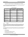
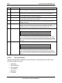
Revision History
Intel® Server Board SE7501WV2 TPS
Revision History
Date
11/02
Revision
Number
0.5
Modifications
First draft for internal review based on the SE7500WV2 TPS
12/02
1.0
Production Release
Disclaimers
Information in this document is provided in connection with Intel® products. No license, express
or implied, by estoppel or otherwise, to any intellectual property rights is granted by this
document. Except as provided in Intel's Terms and Conditions of Sale for such products, Intel
assumes no liability whatsoever, and Intel disclaims any express or implied warranty, relating to
sale and/or use of Intel products including liability or warranties relating to fitness for a particular
purpose, merchantability, or infringement of any patent, copyright or other intellectual property
right. Intel products are not intended for use in medical, life saving, or life sustaining
applications. Intel may make changes to specifications and product descriptions at any time,
without notice.
Designers must not rely on the absence or characteristics of any features or instructions marked
"reserved" or "undefined." Intel reserves these for future definition and shall have no
responsibility whatsoever for conflicts or incompatibilities arising from future changes to them.
This document contains information on products in the design phase of development. Do not
finalize a design with this information. Revised information will be published when the product
is available. Verify with your local sales office that you have the latest datasheet before
finalizing a design.
The Intel® Server Board SE7501WV2 may contain design defects or errors known as errata
which may cause the product to deviate from published specifications. Current characterized
errata are available on request.
Copyright © Intel Corporation 2003.
*Other brands and names are the property of their respective owners.
Revision 1.0
ii
Intel reference number C25653-001
Intel® Server Board SE7501WV2 TPS
Table of Contents
Table of Contents
1. Introduction ..........................................................................................................17
2. SE7501WV2 Server Board Overview ..................................................................18
2.1
SE7501WV2 Feature Set........................................................................... 18
3. Functional Architecture .......................................................................................21
3.1
Processor and Memory Subsystem ........................................................... 21
3.1.1
Processor Support ..................................................................................... 21
3.1.2
Memory Subsystem ................................................................................... 23
3.2
Intel® E7501 Chipset .................................................................................. 27
3.2.1
MCH Memory Architecture......................................................................... 28
3.2.2
MCH North Bridge...................................................................................... 28
3.2.3
P64H2 ........................................................................................................ 29
3.2.4
ICH3-S ....................................................................................................... 30
3.3
Super I/O ................................................................................................... 32
3.3.1
GPIOs ........................................................................................................ 32
3.3.2
Serial Ports ................................................................................................ 33
3.3.3
BIOS Flash................................................................................................. 37
4. Configuration and Initialization...........................................................................38
4.1.1
Main Memory ............................................................................................. 38
4.1.2
Memory Shadowing ................................................................................... 38
4.1.3
System Management Mode Handling ........................................................ 39
4.2
I/O Map ...................................................................................................... 39
4.3
Accessing Configuration Space ................................................................. 39
4.3.1
CONFIG_ADDRESS Register ................................................................... 39
Revision 1.0
iii
Intel reference number C25653-001
Table of Contents
Intel® Server Board SE7501WV2 TPS
4.4
Hardware Initialization................................................................................ 41
4.5
Clock Generation and Distribution ............................................................. 41
4.6
PCI I/O Subsystem .................................................................................... 44
4.6.1
PCI Subsystem .......................................................................................... 44
4.6.2
P32-A: 32-bit, 33-MHz PCI Subsystem...................................................... 44
4.6.3
P64-B and P64-C: 64-bit, 100-MHz PCI-X Subsystem .............................. 45
4.7
Ultra320 SCSI ............................................................................................ 47
4.8
ATA-100..................................................................................................... 47
4.9
Video Controller ......................................................................................... 48
4.9.1
Video Modes .............................................................................................. 48
4.9.2
Video Memory Interface............................................................................. 49
4.9.3
Front Panel Video Memory ........................................................................ 50
4.10
Network Interface Controller (NIC)............................................................. 50
4.10.1 NIC Connector and Status LEDs ............................................................... 50
4.11
Interrupt Routing ........................................................................................ 50
4.11.1 Legacy Interrupt Routing............................................................................ 51
4.11.2 Serialized IRQ Support .............................................................................. 51
4.11.3 APIC Interrupt Routing............................................................................... 51
5. Server Management .............................................................................................54
5.1
5.1.1
5.2
Sahalee Baseboard Management Controller (BMC).................................. 55
Fault Resilient Booting ............................................................................... 61
System Reset Control ................................................................................ 62
5.2.1
Power-up Reset ......................................................................................... 62
5.2.2
Hard Reset................................................................................................. 62
5.2.3
Soft Reset .................................................................................................. 63
Revision 1.0
iv
Intel reference number C25653-001
Intel® Server Board SE7501WV2 TPS
Table of Contents
5.3
Intelligent Platform Management Buses (IPMB) ........................................ 63
5.4
Inter Chassis Management Bus (ICMB)..................................................... 63
5.5
Error Reporting .......................................................................................... 64
5.5.1
Error Sources and Types ........................................................................... 64
5.5.2
PCI Bus Errors ........................................................................................... 64
5.5.3
Intel® Xeon™ Processor Bus Errors .......................................................... 64
5.5.4
Memory Bus Errors .................................................................................... 64
5.5.5
Fault and Status LEDs ............................................................................... 64
5.5.6
Temperature Sensors ................................................................................ 70
6. BIOS ......................................................................................................................71
6.1
System Flash ROM Layout ........................................................................ 71
6.2
BIOS Boot Specification Compliance ......................................................... 71
6.3
Memory ...................................................................................................... 72
6.3.1
Memory Configuration................................................................................ 73
6.3.2
Memory Sizing and Initialization................................................................. 73
6.3.3
ECC Initialization........................................................................................ 74
6.3.4
Memory Remapping................................................................................... 74
6.3.5
DIMM Failure LED ..................................................................................... 74
6.4
Processors ................................................................................................. 74
6.5
Extended System Configuration Data (ESCD), Plug and Play (PnP)......... 74
6.5.1
Resource Allocation ................................................................................... 75
6.5.2
PnP ISA Auto-Configuration....................................................................... 75
6.5.3
PCI Auto-Configuration .............................................................................. 76
6.6
NVRAM API ............................................................................................... 76
6.7
Legacy ISA Configuration .......................................................................... 76
Revision 1.0
v
Intel reference number C25653-001
Table of Contents
Intel® Server Board SE7501WV2 TPS
6.8
Automatic Detection of Video Adapters ..................................................... 76
6.9
Keyboard / Mouse Configuration................................................................ 77
6.9.1
Boot without Keyboard and/or Mouse ........................................................ 77
6.10
Floppy Drives ............................................................................................. 77
6.11
Universal Serial Bus (USB) ........................................................................ 78
6.12
BIOS Supported Server Management Features ........................................ 78
6.12.1 IPMI ........................................................................................................... 78
6.12.2 Advanced Configuration and Power Interface (ACPI) ................................ 79
6.12.3 Wake Events.............................................................................................. 80
6.12.4 Front Panel Switches ................................................................................. 80
6.12.5 Wired For Management (WFM) ................................................................. 81
6.12.6 PXE BIOS Support..................................................................................... 82
6.12.7 BIOS Recommendations............................................................................ 82
6.13
Console Redirection................................................................................... 82
6.13.1 Operation ................................................................................................... 83
6.13.2 Keystroke Mappings .................................................................................. 83
6.13.3 Limitations.................................................................................................. 86
6.14
Emergency Management Port (EMP) ........................................................ 87
6.14.1 Serial Ports ................................................................................................ 87
6.14.2 Interaction with BIOS Console Redirection ................................................ 87
6.15
Service Partition Boot ................................................................................ 87
6.16
System Management BIOS (SMBIOS) ...................................................... 88
6.17
Microsoft* Windows* Compatibility............................................................. 90
6.17.1 Quiet Boot .................................................................................................. 91
6.18
BIOS Serviceabilty Features ...................................................................... 91
Revision 1.0
vi
Intel reference number C25653-001
Intel® Server Board SE7501WV2 TPS
Table of Contents
6.18.1 CMOS Reset.............................................................................................. 91
6.19
BIOS Updates ............................................................................................ 92
6.19.1 Flash Update Utility .................................................................................... 92
6.19.2 Loading the System BIOS.......................................................................... 93
6.19.3 User Binary Area........................................................................................ 93
6.19.4 BIOS Recovery Mode ................................................................................ 93
6.19.5 Rolling BIOS and On-line updates ............................................................. 94
6.20
BIOS and System Setup ............................................................................ 95
6.20.1 BIOS Setup Utility ...................................................................................... 95
6.20.2 Setup Utility Operation ............................................................................... 96
6.21
BIOS Security Features ........................................................................... 109
6.21.1 Operating Model ...................................................................................... 109
6.22
Password Protection ................................................................................ 110
6.23
Inactivity Timer......................................................................................... 111
6.24
Hot Key Activation.................................................................................... 111
6.25
Password Clear Jumper........................................................................... 111
6.26
Secure Mode (Unattended start).............................................................. 111
6.27
Front Panel Lock...................................................................................... 111
6.28
Video Blanking ......................................................................................... 111
6.29
PS/2 Keyboard and Mouse Lock.............................................................. 112
6.30
Secure Boot (Unattended Start)............................................................... 112
6.31
Error Handling.......................................................................................... 112
6.31.1 Error Sources and Types ......................................................................... 112
6.32
SMI Handler ............................................................................................. 113
6.33
PCI Bus Error........................................................................................... 113
Revision 1.0
vii
Intel reference number C25653-001
Table of Contents
Intel® Server Board SE7501WV2 TPS
6.34
Processor Bus Error................................................................................. 113
6.35
Single-Bit ECC Error Throttling Prevention .............................................. 113
6.36
System Limit Error ................................................................................... 114
6.37
Boot Event ............................................................................................... 114
6.38
Fault Resilient Booting (FRB)................................................................... 114
6.38.1 FRB3........................................................................................................ 114
6.38.2 FRB2........................................................................................................ 114
6.39
Boot Monitoring........................................................................................ 116
6.39.1 Purpose.................................................................................................... 116
6.40
Logging Format Conventions ................................................................... 118
6.40.1 Memory Error Events ............................................................................... 118
6.40.2 PCI Error Events ...................................................................................... 120
6.40.3 FRB-2 Error Events.................................................................................. 121
6.41
POST Codes, Error Messages, and Error Codes .................................... 122
6.41.1 POST Progress Code LEDs..................................................................... 122
6.41.2 POST Error Codes and Messages........................................................... 123
6.41.3 POST Error Beep Codes.......................................................................... 125
6.41.4 BIOS Recovery Beep Codes.................................................................... 125
6.41.5 Bootblock Error Beep Codes.................................................................... 126
6.42
"POST Error Pause" Option ..................................................................... 127
6.43
SE7501WV2 Server Board BIOS Runtime APIs ...................................... 127
6.44
INT 15 Extensions.................................................................................... 127
6.44.1 Cache Services........................................................................................ 127
6.44.2 Intel ID String ........................................................................................... 128
6.44.3 Processor Information.............................................................................. 129
Revision 1.0
viii
Intel reference number C25653-001
Intel® Server Board SE7501WV2 TPS
Table of Contents
6.44.4 Extended NVRAM Services ..................................................................... 129
6.44.5 IPMB Services ......................................................................................... 130
6.44.6 INT15h, Function DA20h, Subfunction 99h/9Ah/9Bh – Read/Write/Bus
Master Write IMB .................................................................................................. 130
6.45
Multiple Processor Support (MPS)........................................................... 130
6.45.1 Multiprocessor Specification Support ....................................................... 130
6.45.2 Multiple Processor Support ...................................................................... 131
6.45.3 Mixed Processor Support......................................................................... 131
6.46
Hyper-Threading Technology................................................................... 132
6.47
OEM Customization ................................................................................. 132
6.48
User Binary .............................................................................................. 132
6.48.1 Scan Point Definitions .............................................................................. 134
6.48.2 Format of the User Binary Information Structure...................................... 135
6.48.3 OEM Splash Screen ................................................................................ 135
6.48.4 Localization .............................................................................................. 135
7. SE7501WV2 ACPI Implementation....................................................................136
7.1
ACPI ........................................................................................................ 136
7.1.1
Front Panel Switches ............................................................................... 136
7.1.2
Wake up Sources (ACPI and Legacy) ..................................................... 138
8. SE7501WV2 Connectors....................................................................................139
8.1
Power Connectors ................................................................................... 139
8.2
Memory Module Connector...................................................................... 140
8.3
Processor Socket..................................................................................... 141
8.4
System Management Headers................................................................. 143
8.4.1
ICMB Header ........................................................................................... 143
8.4.2
OEM IPMB Header .................................................................................. 143
Revision 1.0
ix
Intel reference number C25653-001
Table of Contents
Intel® Server Board SE7501WV2 TPS
8.5
PCI I/O Riser Slot Connector ................................................................... 143
8.6
Front Panel Connectors ........................................................................... 146
8.6.1
High Density 100-Pin Floppy / Front Panel / IDE Connector (J2G1)........ 148
8.6.2
VGA Connector........................................................................................ 150
8.6.3
SCSI Connectors ..................................................................................... 150
8.6.4
NIC Connector ......................................................................................... 151
8.6.5
ATA RAID Connectors ............................................................................. 152
8.6.6
USB Connector ........................................................................................ 153
8.6.7
Floppy Connector..................................................................................... 154
8.6.8
Serial Port Connector............................................................................... 155
8.6.9
Keyboard and Mouse Connector ............................................................. 155
8.7
8.7.1
Miscellaneous Headers............................................................................ 156
Fan Headers ............................................................................................ 156
9. Configuration Jumpers......................................................................................157
9.1
System Recovery and Update Jumpers................................................... 157
9.2
External RJ45 Serial Port Jumper Block .................................................. 158
10. General Specifications.......................................................................................159
10.1
Absolute Maximum Ratings ..................................................................... 159
10.2
Power Information.................................................................................... 159
10.2.1 SE7501WV2 Server Board Power Budget ............................................... 159
10.3
Power Supply Specifications.................................................................... 160
10.3.1 Power Timing ........................................................................................... 160
10.3.2 Voltage Recovery Timing Specifications .................................................. 163
11. Regulatory and Integration Information ...........................................................164
11.1
Product Regulatory Compliance .............................................................. 164
Revision 1.0
x
Intel reference number C25653-001
Intel® Server Board SE7501WV2 TPS
Table of Contents
11.1.1 Product Safety Compliance...................................................................... 164
11.1.2 Product EMC Compliance........................................................................ 164
11.1.3 Product Regulatory Compliance Markings ............................................... 164
11.2
Electromagnetic Compatibility Notices ..................................................... 165
11.2.1 Europe (CE Declaration of Conformity).................................................... 165
11.2.2 Australian Communications Authority (ACA) (C-Tick Declaration of
Conformity)............................................................................................................ 165
11.2.3 Ministry of Economic Development (New Zealand) Declaration of
Conformity............................................................................................................. 165
11.2.4 BSMI (Taiwan) ......................................................................................... 165
11.3
Replacing the Back up Battery................................................................. 165
12. Mechanical Specifications.................................................................................167
12.1
PCI Riser Cards ....................................................................................... 168
12.1.1 1-Slot 3.3V PCI Riser Card ...................................................................... 168
12.1.2 3-Slot 3.3V PCI Riser Card ...................................................................... 168
Appendix A: Glossary.............................................................................................169
Revision 1.0
xi
Intel reference number C25653-001
List of Figures
Intel® Server Board SE7501WV2 TPS
List of Figures
Figure 1. Intel® Server Board SE7501WV2 Block Diagram........................................... 20
Figure 2. Memory Sub-system Block Diagram ............................................................. 24
Figure 3. Memory Bank Label Definition ...................................................................... 26
Figure 4. Serial Port Mux Logic ..................................................................................... 35
Figure 5. J5A2 Jumper Block for DCD Signal ............................................................... 36
Figure 6. J5A2 Jumper Block for DSR Signal................................................................ 36
Figure 7. CONFIG_ADDRES Register .......................................................................... 40
Figure 8. Intel® Server Board SE7501WV2 Clock Distribution ...................................... 43
Figure 9. Intel® Server Board SE7501WV2 Sahalee BMC Block Diagram.................... 54
Figure 10. BIOS Boot Monitoring Flowchart ................................................................ 117
Figure 11. Intel® Server Board SE7501WV2 Configuration Jumpers (J1D4) .............. 157
Figure 12. Output Voltage Timing ............................................................................... 161
Figure 13. Turn On / Off Timing .................................................................................. 162
Figure 14. Intel® Server Board SE7501WV2 Mechanical Drawing .............................. 167
Figure 15. 1-Slot PCI Riser Mechanical Drawing ........................................................ 168
Figure 16. 3-Slot PCI Riser Mechanical Drawing ........................................................ 168
Revision 1.0
xii
Intel reference number C25653-001
Intel® Server Board SE7501WV2 TPS
List of Tables
List of Tables
Table 1. Intel® Server Board SE7501WV2 Processor Support Matrix for 533MHz ....... 21
Table 2. Intel® Server Board SE7501WV2 Processor Support Matrix for 400MHz ....... 22
Table 3. Memory Bank Labels....................................................................................... 25
Table 4. P64-B Speeds ................................................................................................. 29
Table 5. P64-C Speeds ................................................................................................. 30
Table 6. Super I/O GPIO Usage Table.......................................................................... 32
Table 7. Serial A Header Pin-out................................................................................... 34
Table 8. Rear Serial Port B Adapter Pinout................................................................... 36
Table 9. PCIdevice IDs.................................................................................................. 40
Table 10. PCI Bus Segment Characteristics ................................................................. 44
Table 11. P32-A Configuration IDs................................................................................ 44
Table 12. P32-Arbitration Connections.......................................................................... 45
Table 13. P64-B Configuration IDs................................................................................ 45
Table 14. P64-C Configuration IDsIDs .......................................................................... 45
Table 15. P64-B Arbitration Connections ...................................................................... 46
Table 16. P64-C Arbitration Connections ...................................................................... 46
Table 17. Video Modes ................................................................................................ 49
Table 18. Video Memory Interface ................................................................................ 49
Table 19. Interrupt Definitions ....................................................................................... 51
Table 20. Intel® Server Board SE7501WV2 Interrupt Mapping ..................................... 52
Table 21. BMC Pinout ................................................................................................... 55
Table 22. ADM1026 Input Definition.............................................................................. 60
Table 23. Intel® Server Board SE7501WV2 I2C Address Map...................................... 63
Table 24. System Status LEDs ..................................................................................... 65
Table 25. Boot Block POST Progress Codes................................................................ 67
Table 26. Allowed Combinations of Floppy Drive and Floppy Media............................. 77
Table 27. Supported Wake Events................................................................................ 80
Table 28. Non-ASCII Key Mappings............................................................................. 84
Table 29. ASCII Key Mappings ..................................................................................... 86
Table 30. SMBIOS Header Structure ............................................................................ 89
Revision 1.0
xiii
Intel reference number C25653-001
List of Tables
Intel® Server Board SE7501WV2 TPS
Table 31. Setup Utility Screen....................................................................................... 97
Table 32. Keyboard Command Bar ............................................................................... 97
Table 33. Main Menu Selections ................................................................................... 99
Table 34. Primary Master and Slave Adapters Sub-menu Selections ......................... 100
Table 35. Processor Settings Sub-menu..................................................................... 100
Table 36. Advanced Menu Selections ......................................................................... 101
Table 37. Advanced Chipset Control Sub-menu Selections........................................ 101
Table 38. PCI Configuration Sub-menu Selections .................................................... 101
Table 39. PCI Device, Embedded Devices ................................................................. 102
Table 40. I/O Device/Peripheral Configuration Sub-menu Selections ........................ 102
Table 41. Memory Configuration Menu Selections...................................................... 103
Table 42. Security Menu Selections ............................................................................ 103
Table 43. Server Menu Selections .............................................................................. 104
Table 44. System Management Sub-menu Selections................................................ 105
Table 45. Serial Console Redirection Sub-menu Selections ....................................... 106
Table 46. Event Log Configuration Sub-menu Selections ........................................... 106
Table 47. Fault Resilient Boot Sub-menu Selections .................................................. 107
Table 48. Boot Menu Selections ................................................................................. 107
Table 49. Boot Device Priority Selections .................................................................. 107
Table 50. Hard Drive Selections.................................................................................. 108
Table 51. Removable Devices Selections ................................................................... 108
Table 52. Exit Menu Selections ................................................................................... 108
Table 53. Security Features Operating Model............................................................. 109
Table 54. Memory Error Event Data Field Contents.................................................... 119
Table 55. PCI Error Event Data Field Contents........................................................... 120
Table 56. Examples of Event Data Field Contents for PCI Errors ............................... 121
Table 57. FRB-2 Event Data Field Contents ............................................................... 121
Table 58. Examples of Event Data Field Contents for FRB-2 Errors.......................... 122
Table 59. POST Progress Code LED Example ........................................................... 123
Table 60. Standard POST Error Messages and Codes............................................... 123
Table 61. Extended POST Error Messages and Codes .............................................. 124
Table 62. BIOS Recovery Beep Codes ....................................................................... 125
Table 63. Bootblock Error Beep Codes ....................................................................... 126
Revision 1.0
xiv
Intel reference number C25653-001
Intel® Server Board SE7501WV2 TPS
List of Tables
Table 64. Three-beep Boot Block Memory Failure Error Codes.................................. 126
Table 65. Interrupt 15h Extensions.............................................................................. 127
Table 66. User Binary Area Scan Point Definitions ..................................................... 134
Table 67. User Binary Information Structure ............................................................... 135
Table 68. Supported Wake Events.............................................................................. 138
Table 69. Power Connector Pin-out (J3J1) ................................................................. 139
Table 70. Power Supply Signal Connector (J1J1) ....................................................... 139
Table 71. 12V Power Connector (J4J1) ...................................................................... 139
Table 72. DIMM Connectors (J5F1, J5F2, J5F3, J6F1, J6F2, J6F3) .......................... 140
Table 73. Socket 604 Processor Socket Pinout .......................................................... 141
Table 74. ICMB Header Pin-out (J9B2)....................................................................... 143
Table 75. IPMB Header Pin-out (J9C1)....................................................................... 143
Table 76. P64-B Full Length PCI Riser Slot Pin-out .................................................... 143
Table 77. P64-C Low-Profile Riser Slot Pin-out .......................................................... 144
Table 78. 34-pin Front Panel Connector Signal Descriptions ...................................... 146
Table 79. SSI Compliant 24-pin Front Panel Connector Pinout (J1H1)...................... 148
Table 80. High density 100-Pin Floppy/Front Panel/IDE Connector Pin out (J2G1).... 148
Table 81. VGA Connector Pin-out (J8A1) ................................................................... 150
Table 82. 68-pin VHDCI SCSI and Wide Connectors Pin-out (J7B1, J7A1)................ 150
Table 83. Stacked Dual RJ-45 Connector Pin-out (JA6A1)......................................... 151
Table 84. ATA-100 RAID 40-pin Connectors Pin-out (J1D1, J1D2) ............................ 152
Table 85. ATA-100 Legacy 40-pin Connector Pinout (J1G2) ...................................... 153
Table 86. USB Connectors Pin-out (J4A1, J9A1)........................................................ 153
Table 87. Optional USB Connection Header Pin-out (J1D3)...................................... 154
Table 88. Legacy 34-pin Floppy Connector Pin-out (J1G1) ........................................ 154
Table 89. Rear Low-Profile RJ-45 Serial B Port Pin-out (J5A1) .................................. 155
Table 90. 9-pin Header Serial A Port Pin-out (J9A2)................................................... 155
Table 91. Keyboard and Mouse PS/2 Connector Pin-out (J6A1) ................................ 156
Table 92. Three-pin Fan Headers Pin-out (J4J2, J7J1)............................................... 156
Table 93. Fan Pack Fan Header Pin-out (J3J2) .......................................................... 156
Table 94. Configuration Jumper Options..................................................................... 157
Table 95. Absolute Maximum Ratings......................................................................... 159
Table 96. Intel® Server Board SE7501WV2/SR2300/SR1300 Power Budget ............. 159
Revision 1.0
xv
Intel reference number C25653-001
List of Tables
Intel® Server Board SE7501WV2 TPS
Table 97. Intel® Server Board SE7501WV2 Static Power Supply Voltage Specification160
Table 98. Intel® Server Board SE7501WV2 Dynamic Power Supply Voltage
Specification.......................................................................................................... 160
Table 99. Voltage Timing Parameters ......................................................................... 161
Table 100. Turn On / Off Timing.................................................................................. 161
Revision 1.0
xvi
Intel reference number C25653-001
Intel® Server Board SE7501WV2 TPS
1.
Introduction
Introduction
The Intel® SE7501WV2 server board Technical Product Specification (TPS) provides a highlevel technical description for the Intel® SE7501WV2 server board. It details the architecture and
feature set for all functional sub-systems that make up the server board.
This document is sub-divided into the following main categories:
Chapter 2: SE7501WV2 Server Board Overview
Chapter 3: Functional Architecture
Chapter 4: Configuration and Initialization
Chapter 5: Server Management
Chapter 6: BIOS
Chapter 7: SE7501WV2 Server Board ACPI Implementation
Chapter 8: SE7501WV2 Server Board Connectors
Chapter 9: Configuration Jumpers
Chapter 10: General Specifications
Chapter 11: Regulatory and Integration Information
Chapter 12: Mechanical Specification
The contents of this document are derived from several of the SE7501WV2’s External Product
Specifications (EPS). For a more detailed, lower level description of a particular functional subsystem, the EPS for the sub-system should be ordered from your Intel field representative. The
EPS documents available for the SE7501WV2 server board include the following:
•
•
•
Intel® SE7501WV2 server board BIOS EPS
Intel® SE7501WV2 server board Baseboard Management Controller EPS
Sahalee Core BMC EPS for IPMI v1.5 System
The SE7501WV2 server board supports the Intel® Server Management Version 5.5 software.
One additional EPS document is available to provide technical detail on the feature set of the
server management software. This document is:
• ISM Customization EPS
Revision 1.0
17
Intel reference number C25653-001
SE7501WV2 Server Board Overview
2.
Intel® Server Board SE7501WV2
SE7501WV2 Server Board Overview
The SE7501WV2 server board is a monolithic printed circuit board with features that were
designed to support the high-density 1U and 2U server market.
2.1
SE7501WV2 Feature Set
Two different SE7501WV2 server boards will be made available. One will provide an embedded
Ultra-320* SCSI interface and the other will provide an embedded ATA-100* “Value-Raid”
interface. Both boards support the following feature set:
•
•
•
Dual Intel® Xeon™ processor in the Socket 604 INT3/FCPGA package
533 MHz Front Side Bus
Intel® E7501 chipset
- E7501 North Bridge
- P64H2 I/O Bridge
- ICH3-S South Bridge
•
Support for up to six DDR266 compliant registered ECC DIMMs providing up to 12 GB of
memory, when 2G DIMMs become available and have been tested. (Will support
DDR200 modules when 400MHz processors are installed.)
Three separate and independent PCI buses:
•
-
Segment A: 32-bit, 33 MHz, 5 V (P32-A) with two embedded devices:
•
2D/3D graphics controller: ATI Rage* XL Video Controller with 8 MB of
memory
•
ATA-100 controller: Promise Technology* PDC20277 (ATA-100 board only)
-
Segment B: 64-bit, 133 MHz, 3.3 V, PCI-X (P64-B) supporting the following
configuration:
•
One PCI I/O riser slot capable of supporting full length PCI add-in cards
•
Dual-channel Intel® 10/100/1000 82546EB Gigabit Ethernet Controller
-
Segment C: 64-bit, 133 MHz, 3.3 V PCI-X (P64-C) supporting the following
devices:
•
One PCI I/O riser slot capable of supporting low-profile PCI add-in cards
•
Dual-channel SCSI with Zero Channel RAID (ZCR) and host RAID support
(SCSI SKU only)
•
LPC (Low Pin Count) bus segment with two embedded devices:
- Platform Management Controller (PMC) providing monitoring, alerting, and
logging of critical system information obtained from embedded sensors on the
server board
- Super I/O controller chip providing all PC-compatible I/O (floppy, serial,
keyboard, mouse)
•
X-Bus segment with one embedded device:
Revision 1.0
18
Intel reference number C25653-001
Intel® Server Board SE7501WV2 TPS
•
•
•
•
•
•
•
SE7501WV2 Server Board Overview
- Flash ROM device for system BIOS: Intel® 32-megabit 28F320C3 Flash ROM
Two external Universal Serial Bus (USB) ports with an additional internal header
providing two optional USB ports for front panel support
One external low-profile RJ45 serial port. An internal header is also available providing
an optional serial port.
One IDE connector, supporting one or two ATA-100 compatible devices
Support for up to seven system fans
Fault/Status LEDs throughout the server board
Multiple server management headers providing on-board interconnects to server
management features
SSI-compliant connectors for SSI interface support: front panel, floppy, and ATA-33
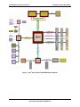
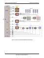
Figure 1 shows the functional blocks of the server board and the plug-in modules that it
supports.
Revision 1.0
19
Intel reference number C25653-001
SE7501WV2 Server Board Overview
Intel® Server Board SE7501WV2
Figure 1. Intel® Server Board SE7501WV2 Block Diagram
Revision 1.0
20
Intel reference number C25653-001
Intel® Server Board SE7501WV2 TPS
3.
Functional Architecture
Functional Architecture
This chapter provides a high-level description of the functionality distributed between the
architectural blocks of the SE7501WV2 server board.
3.1
Processor and Memory Subsystem
The E7501 chipset provides a 36-bit address, 64-bit data processor host bus interface,
operating at 400MHz and 533Mz in the AGTL+ signaling environment. The MCH component of
the chipset provides an integrated memory controller, an 8-bit Hub Interface, and three 16-bit
Hub Interfaces.
The Hub Interface provides the interface to two 64-bit, 133-MHz, Rev 1.0 compliant PCI-X
buses via the P64H2. The SE7501WV2 server board directly supports up to 12 GB of ECC
memory, using six DDR266 compliant registered ECC DIMMs. (Will support DDR200 modules
when 400MHz processors are installed.) The ECC implementation in the MCH can detect and
correct single-bit errors, detect multiple-bit errors, and support the Intel® Single Device Data
Correction features.
3.1.1
Processor Support
The SE7501WV2 server board supports one or two Intel® Xeon™ processors in the Socket 604
INT3/FCPGA package. When two processors are installed, all processors must be of identical
revision, core voltage, and bus/core speed. When only one processor is installed, it should be in
the socket labeled CPU-1 and the other socket must be empty. The support circuitry on the
server board consists of the following:
•
•
Dual Socket 604 INT3/FCPGA CPU sockets supporting 533 MHz (will support 400 MHz
processors running at 400 Mhz speed.)
Processor host bus AGTL+ support circuitry
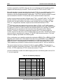
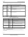
Table 1. Intel® Server Board SE7501WV2 Processor Support Matrix for 533MHz
Speed (MHz)
533MHz
2.8 GHz (1U)
2.8 GHz (1U)
2.8 GHz
2.8gGHz
2.66 GHz (1U)
2.66 GHz (1U)
2.66 GHz
2.66 GHz
2.4 GHz (1U)
2.4 GHz (1U)
2.4 GHz
2.4 GHz
2.0 GHz (1U)
2.0 GHz (1U)
2.0 GHz
2.0 GHz
Product Code
BX80532KE2800DU
BX80532KE2800DU
BX80532KE2800D
BX80532KE2800D
BX80532KE2667DU
BX80532KE2667DU
BX80532KE2667D
BX80532KE2667D
BX80532KE2400DU
BX80532KE2400DU
BX80532KE2400D
BX80532KE2400D
BX80532KE2000DU
BX80532KE2000DU
BX80532KE2000D
BX80532KE2000D
MM#
851292
851275
851275
851285
851650
851713
851647
851712
851290
851273
851280
851269
851288
851272
851279
851268
Test
Specification
(S-spec)
SL6GG
SL6NS
SL6NS
SL6GG
SL6GF
SL6NR
SL6GF
SL6GF
SL6GD
SL6NQ
SL6GD
SL6NQ
SL6RQ
SL6NP
SL6NP
SL6NP
Stepping
C1
C1
C1
C1
C1
C1
C1
C1
C1
C1
C1
C1
C1
C1
C1
C1
Revision 1.0
CPUID
0F24
0F24
0F24
0F24
0F24
0F24
0F24
0F24
0F24
0F24
0F24
0F24
0F24
0F24
0F24
0F24
L2
Cache
Size
512k
512k
512k
512k
512k
512k
512k
512k
512k
512k
512k
512k
512k
512k
512k
512k
Notes
1
1
1
1
1
1
1
1
1
1
1
1
1
1
1
1
21
Intel reference number C25653-001
Functional Architecture
Intel® Server Board SE7501WV2
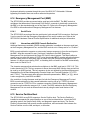
Table 2. Intel® Server Board SE7501WV2 Processor Support Matrix for 400MHz
Speed (MHz)
400MHz
2.8 GHz
2.8 GHz
2.8GHz (1U)
2.6 GHz
2.6 GHz
2.6 GHz (1U)
2.4 GHz
2.4 GHz
2.4 GHz
2.4 GHz (1U)
2.2 GHz
2.2 GHz
2.2 GHz
2.2 GHz (1U)
2.0 GHz
2.0 GHz
1.8 GHz
1.8 GHz
1.8 GHz (1U)
Product Code
MM#
BX80532KC2800D
80532KC072512
BX80532KC2800DU
BX80532KC2600D
80532KC064512
BX80532KC2600DU
BX80532KC2400D
80532KC056512
BX80532KC2400D
BX80532KC2400DU
BX80532KC2200D
80532KC049512
BX80532KC2200D
BX80532KC2200DU
BX80532KC2000D
80532KC041512
BX80532KC1800D
80532KC033512
BX80532KC1800DU
850007
849546
850614
850609
847694
849701
845163
847695
851738
849703
843623
849112
49356
848431
843637
849063
843620
849064
848419
Test
Specification
(S-spec)
SL6MS
SL6M7
SL6M7
SL6EQ
SL6EQ
SL6EQ
SL687
SL6EP
SL6EP
SL6K2
SL624
SL6JZ
SL6JZ
SL624
SL623
SL6JY
SL622
SL6JX
SL622
Stepping
C1
C1
C1
C1
C1
C1
tB0
C1
C1
B0
tB0
C1
C1
tB0
tB0
C1
tB0
C1
tB0
CPUID
0F24
0F24
0F24
0F24
0F24
0F24
0F24
0F24
0F24
0F24
0F24
0F24
0F24
0F24
0F24
0F24
0F24
0F24
0F24
L2
Cache
Size
512k
512k
512k
512k
512k
512k
512k
512k
512k
512k
512k
512k
512k
512k
512k
512k
512k
512k
512k
Notes
1
1
1
1
1
1
1
1
1
1
1
1
1
1
1
1
1
1
1
Notes: Processors must be populated in sequential order. That is, CPU socket #1 must be
populated before CPU socket #2.
•
•
The SE7501WV2 server board is designed to provide up to 75 A per processor.
Processors with higher current requirements are not supported.
Processor terminators are not required in unpopulated processor sockets.
In addition to the circuitry described above, the processor subsystem contains the following:
•
•
3.1.1.1
Processor module presence detection logic
Server management registers and sensors
Processor VRM
The SE7501WV2 baseboard has a single VRM (Voltage Regulator Module) to support two
processors. It is compliant with the VRM 9.1 specification and provides a maximum of 150
AMPs, which is capable of supporting currenlyt supported processors as well as those
supported in the future.
The board hardware and BMC must read the processor VID (voltage identification) bits for each
processor before turning on the VRM. If the VIDs of the two processors are not identical, then
the BMC will not turn on the VRM and a beep code is generated.
Revision 1.0
22
Intel reference number C25653-001
Intel® Server Board SE7501WV2 TPS
3.1.1.2
Functional Architecture
Reset Configuration Logic
The BIOS determines the processor stepping, cache size, etc through the CPUID instruction.
The requirements are that all processors in the system must operate at the same frequency,
have the same cache sizes, and have the same VID. No mixing of product families is supported.
On the SE7501WV2 platform, the BIOS is responsible for configuring the processor speeds.
The processor information is read at every system power-on. The speed is set to correspond to
the speed of the slowest processor installed.
Note: No manual processor speed setting options exist either in the form of a BIOS setup option
or jumpers when using production level processors.
3.1.1.3
Processor Module Presence Detection
Logic is provided on the baseboard to detect the presence and identity of installed processors.
The BMC checks the logic and will not turn on the system DC power unless the VIDs of both
processors match in a dual processor configuration.
3.1.1.4
Interrupts and APIC
Interrupt generation and notification to the processors is done by the APICs in the ICH3 and the
P64H2 using messages on the front side bus.
3.1.1.5
Server Management Registers and Sensors
The Baseboard Management Controller manages registers and sensors associated with the
processor / memory subsystem. For more information, refer to Section 5.
3.1.2
Memory Subsystem
The SE7501WV2 server board supports up to six DIMM slots for a maximum memory capacity
of 12 GB. The DIMM organization is x72, which includes eight ECC check bits. The memory
interface runs at 266MHz. (200MHz when DDR200 DRAM’s and 400MHz processors are used.)
The memory controller supports memory scrubbing, single-bit error correction, multiple-bit error
detection, and the Intel® Single Device Data Correction feature. Memory can be implemented
with either single sided (one row) or double-sided (two row) DIMMs.
The following figure provides a block diagram of the memory sub-system implemented on the
SE7501WV2 server board.
Revision 1.0
23
Intel reference number C25653-001
Functional Architecture
Intel® Server Board SE7501WV2
Figure 2. Memory Sub-system Block Diagram
3.1.2.1
Memory DIMM Support
The SE7501WV2 server board supports DDR266 compliant registered ECC DIMMs operating at
266MHz. (DDR200 DIMMs are supported when 400MHz processors are used.)
Only DIMMs tested and qualified by Intel or a designated memory test vendor are supported on
the SE7501WV2 server board. A list of tested DIMMs will be made available. Note that all
DIMMs are supported by design, but only fully tested DIMMs will be supported.
The minimum supported DIMM size is 128 MB. Therefore, the minimum main memory
configuration is 2 x 128 MB or 256 MB. The largest size DIMM supported is a 2 GB stacked
registered DDR266 ECC DIMM based on 512 megabit technology. (DDR200 DIMMs are
supported when 400MHz processors are used)
Only registered DDR266 compliant, ECC, DDR memory DIMMs will be supported. (DDR200
DIMMs are supported when 400MHz processors are used.)
• ECC single-bit errors will be corrected and multiple-bit errors will be detected. The
SE7501WV2 server board also supports the Intel® Single Device Data Correction
feature.
• The maximum memory capacity is 12 GB.
• The minimum memory capacity is 256 MB.
3.1.2.2
Memory Configuration
The memory interface between the MCH and DIMMs is 144 bits wide. This requires that two
DIMMs be populated per bank in order for the system to operate. At least one bank has to be
Revision 1.0
24
Intel reference number C25653-001
Intel® Server Board SE7501WV2 TPS
Functional Architecture
populated in order for the system to boot. If additional banks have less than two DIMMs, the
memory for that bank(s) will not be available to the system.
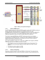
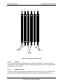
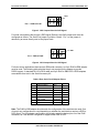
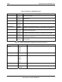
There are three banks of DIMMs, labeled 1, 2, and 3. Bank 1 contains DIMM locations 1A and
1B, Bank 2 contains 2A and 2B, and Bank 3 contains 3A and 3B. DIMM socket identifiers are
marked with silkscreen next to each DIMM socket on the baseboard. Note that the sockets
associated with any given bank are located next to each other.
Certain combinations of DIMM types in the same system can violate the write Ringback
measurement specification during analog validation.
• When mixing double-ranked DIMMs (x4 or x8) with single-ranked DIMMs (x4 or x8), if a
single-ranked DIMM is placed in the populated slot closest to the MCH, the Write Ringback
at that DIMM violates the JEDEC DRAM specification.
The baseboard’s signal integrity and cooling are optimized when memory banks are populated
in order. Therefore, when installing memory, DIMMs should be installed starting with Bank 1 and
ending with Bank 3.
DIMM and memory configurations must adhere to the following:
•
•
•
•
•
•
•
•
•
DDR266 registered ECC DIMM modules (DDR200 when 400MHz processors are used)
DIMM organization: x72 ECC
Pin count: 184
DIMM capacity: 128 MB, 256 MB, 512 MB, 1 GB, 2 GB
Serial PD: JEDEC Rev 2.0
Voltage options: 2.5 V (VDD/VDDQ)
Interface: SSTL2
Two DIMMs must be populated in a bank for a x144 wide memory data path.
Any or all memory banks may be populated.
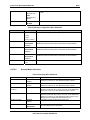
Table 3. Memory Bank Labels
Memory DIMM
Bank
J5F1 (DIMM 1B), J5F2 (DIMM 1A)
1
J5F3 (DIMM 2B), J6F1 (DIMM 2A)
2
J6F2 (DIMM 3B), J6F3 (DIMM 3A)
3
Revision 1.0
25
Intel reference number C25653-001
Functional Architecture
Intel® Server Board SE7501WV2
J5F1
J5F2
J5F3
J6F1
J6F2
J6F3
1B
1A
2B
2A
3B
3A
Bank 1
Bank 3
Bank 2
Figure 3. Memory Bank Label Definition
3.1.2.3
I2C*Bus
An I2C* bus connects the six DIMM slots to the ICH3-S and the BMC. This bus is used by the
system BIOS to retrieve DIMM information needed to program the MCH memory registers which
are required to boot the system.
3.1.2.4
DIMM Failure LED
The SE7501WV2 server board provides DIMM Failure LEDs located next to each DIMM slot on
the baseboard. The DIMM Failure LEDs are used to indicate double-bit DIMM errors. If a
Revision 1.0
26
Intel reference number C25653-001
Intel® Server Board SE7501WV2 TPS
Functional Architecture
double-bit error is detected during POST, the BIOS sends a Set DIMM State command to the
BMC indicating that the DIMM LED is lit.
3.1.2.5
Intel® Single Device Data Correction feature
The SE7501WV2 server board supports Intel’s Single Device Data Correction correct memory
architecture, which gives the memory sub-system the ability to withstand a multi-bit failure within
a DRAM device, including a failure that causes incorrect data on all data bits of the device.
3.2
Intel® E7501 Chipset
The SE7501WV2 server board is designed around the Intel® E7501 chipset. The chipset
provides an integrated I/O bridge and memory controller, and a flexible I/O subsystem core
(PCI-X). This is targeted for multiprocessor systems and standard high-volume servers. The
Intel E7501 chipset consists of three components:
•
MCH: Memory Controller Hub North Bridge. The MCH North Bridge accepts access
requests from the host (processor) bus and directs those accesses to memory or to one
of the PCI buses. The MCH monitors the host bus, examining addresses for each
request. Accesses may be directed to a memory request queue for subsequent
forwarding to the memory subsystem, or to an outbound request queue for subsequent
forwarding to one of the PCI buses. The MCH also accepts inbound requests from the
P64H2 and the ICH3-S. The MCH is responsible for generating the appropriate controls
to control data transfer to and from memory.
•
P64H2: PCI-X 64bit Hub 2.0 I/O Bridge. The P64H2 provides the interface for two 64bit, 133MHz Rev. 1.0 compliant PCI-X buses. The P64H2 is both master and target on
both PCI-X buses.
•
ICH3-S: South Bridge. The ICH3-S controller has several components. It provides the
interface for a 32-bit, 33-MHz Rev. 2.2-compliant PCI bus. The ICH3-S can be both a
master and a target on that PCI bus. The ICH3-S also includes a USB controller and an
IDE controller. The ICH3-S is also responsible for much of the power management
functions, with ACPI control registers built in. The ICH3-S also provides a number of
GPIO pins and has the LPC bus to support low speed legacy I/O.
The MCH, P64H2, and ICH3-S chips provide the pathway between processor and I/O systems.
The MCH is responsible for accepting access requests from the host (processor) bus, and
directing all I/O accesses to one of the PCI buses or legacy I/O locations. If the cycle is directed
to one of the 64-bit PCI segments, the MCH communicates with the P64H2 through a private
interface called the HI (Hub Interface). If the cycle is directed to the ICH3-S, the cycle is output
on the MCH’s 8bit HI 1.5 bus. The P64H2 translates the HI 2.0 bus operation to a 64-bit PCI-X
Rev. 1.0-compliant signaling environment operating from 100MHz to 133 MHz. The ICH3-S
translates the HI 1.5 bus operation to a 32-bit PCI Rev. 2.2-compliant signaling environment
operating at 33MHz.
The HI 2.0 bus is 16 bits wide and operates at 66 MHz with 512MT/s, providing over 1 GB per
second of bandwidth.
All I/O for the SE7501WV2 server board, including PCI and PC-compatible I/O, is directed
through the MCH and then through either the P64H2 or the ICH3-S provided PCI buses.
Revision 1.0
27
Intel reference number C25653-001
Functional Architecture
•
•
Intel® Server Board SE7501WV2
The ICH3-S provides a 32-bit/33-MHz PCI bus hereafter called P32-A.
The P64H2 provides two independent 64-bit, 133-MHz PCI-X buses hereafter called
P64-B, and P64-C.
This independent bus structure allows all three PCI buses to operate concurrently.
3.2.1
MCH Memory Architecture
The MCH supports a 144-bit wide Memory Sub-system that can support a maximum of 12 GB
(using 2 GB DIMMs). This configuration needs external registers for buffering the memory
address and control signals. In this configuration the MCH supports six DDR266 compliant
registered stacked DIMMs for a maximum of 12 GB. (DDR200 DIMMs are supported when
400MHz processors are used.) The six chip selects are registered inside the MCH and need no
external registers for chip selects.
The memory interface runs at 266 MHz. (200 MHz when DDR-200 modules and 400 MHz
processors are used.) The memory interface supports a 144-bit wide memory array. It uses
fifteen address lines (BA[1:0] and MA[12:0]) and supports 64 Mb, 128 Mb, 256 Mb, 512 Mb
DRAM densities. The DDR DIMM interface supports memory scrubbing, single-bit error
correction, and multiple bit error detection as well as the Intel® Single Device Data Correction
features.
3.2.1.1
DDR Configurations
The DDR interface supports up to 12GB of main memory and supports single- and double-density
DIMMs.
3.2.2
MCH North Bridge
The E7501 MCH North Bridge (MCH) is a 1005 ball FC-BGA device and uses the proven
components of previous generations like the Intel® Pentium® 4 bus interface unit, the Hub
Interface unit, and the DDR memory interface unit. In addition, the MCH incorporates a Hub
Interface (HI). The hub interface enables the MCH to directly interface with the P64H2. The
MCH also increases the main memory interface bandwidth and maximum memory configuration
with a 144-bit wide memory interface.
The MCH integrates three main functions:
• An integrated high performance main memory subsystem.
• An HI 2.0 bus interface that provides a high-performance data flow path between the
host bus and the I/O subsystem.
• A HI 1.5 bus which provides an interface to the ICH3-S (South Bridge).
Other features provided by the MCH include the following:
• Full support of ECC on the memory bus
• Full support of the Intel® Single Device Data Correction features.
• Twelve deep in-order queue
• Full support of registered DDR266 ECC DIMMs (DDR200 DIMMs when 400MHz
processors are used)
• Support for 12 GB of DDR memory
• Memory scrubbing
Revision 1.0
28
Intel reference number C25653-001
Intel® Server Board SE7501WV2 TPS
3.2.3
Functional Architecture
P64H2
The P64H2 is a 567-ball FCBGA device and provides an integrated I/O bridge that provides a
high-performance data flow path between the HI 2.0 and the 64-bit I/O subsystem. This
subsystem supports peer 64-bit PCI-X segments. Because it has two PCI interfaces, the P64H2
can provide large and efficient I/O configurations. The P64H2 functions as the bridge between
the HI and the two 64-bit PCI-X I/O segments. The HI can support 1 GB/s of data bandwidth.
3.2.3.1
PCI Bus P64-B I/O Subsystem
The P64-B supports the following embedded devices and connectors:
•
One 184-pin, 5-volt keyed, 64-bit PCI expansion slot connector. The expansion slot can
be used for either a 1-slot or a 3-slot PCI riser card. Both riser cards support 184-pin,
3.3V keyed, 64-bit PCI expansion slots. The PCI slots on the P64-B PCI bus support
both full-length PCI cards and low profile PCI cards with the appropriate faceplate.
•
One Intel® 82546EB dual channel 10/100/1000 Ethernet controller.
The BIOS is responsible for setting the bus speed of the P64-B. The following tables show the
bus frequency according to slot population. The bus speed will always be set up to run at the
speed of the slowest card installed.
Table 4. P64-B Speeds
Configuration
Intel® Server ChassisSR1300
Intel® Server Chassis SR2300
(Bus B with Anvik* Dual NIC
down and 1 Slot Riser)
(Bus B with Anvik* Dual NIC
down and 3 Slot Riser)
0 Adapter Cards installed and
on board device enabled
PCI-X 64/100
PCI-X 64/100
1 Adapter Cards installed and
on board device enabled
PCI-X 64/100
PCI-X 64/100
2 Adapter Cards installed and
on board device enabled
N/A
PCI-X 64/100
3 Adapter Cards installed and
on board device enabled
N/A
PCI-X 64/66
1 Adapter Cards installed and
on board device disabled
PCI-X 64/100
PCI-X 64/100
2 Adapter Cards installed and
on board device disabled
N/A
PCI-X 64/100
3 Adapter Cards installed and
on board device disabled
N/A
PCI-X 64/66
3.2.3.2
PCI Bus P64-C I/O Subsystem
P64-C supports the following embedded devices and connectors:
•
One 184-pin, 5-volt keyed, 64-bit PCI expansion slot connector. The expansion slot can
be used for either a 1-slot or a 3-slot PCI riser card. Both riser cards support 184-pin,
3.3V keyed, 64-bit PCI expansion slots. The PCI slots on the P64-C PCI bus support
only low profile PCI cards.
•
One Adaptec* 7902 dual channel U-320 SCSI controller.
Revision 1.0
29
Intel reference number C25653-001
Functional Architecture
•
Intel® Server Board SE7501WV2 TPS
Support for Zero Channel RAID (ZCR) or M-ROMB that allows the on board SCSI
controller to be “hidden” from system and used by the RAID processor on the add-in card.
The BIOS is responsible for setting the bus speed of the P64-C. The bus speed will always be
set up to run at the speed of the slowest card installed.
Table 5. P64-C Speeds
Configuration
Intel® Server Chassis SR1300
Intel® Server Chassis SR2300
(Bus C with AIC7902 SCSI down
and 1 Slot Riser)
(Bus C with AIC7902 SCSI
down and 3 Slot Riser)
0 Adapter Cards installed
and on board device
enabled
PCI-X 100
PCI-X 100
1 Adapter Cards installed
and on board device
enabled
PCI-X 100
PCI-X 100
2 Adapter Cards installed
and on board device
enabled
N/A
PCI-X 100
3 Adapter Cards installed
and on board device
enabled
N/A
PCI-X 64/66
1 Adapter Cards installed
and on board device
disabled
PCI-X 64/100
PCI-X 64/100
2 Adapter Cards installed
and on board device
disabled
N/A
PCI-X 64/100
3 Adapter Cards installed
and on board device
disabled
N/A
PCI-X 64/66
3.2.4
ICH3-S
The ICH3-S is a multi-function device, housed in a 421-pin BGA device, providing a HI 1.5 to
PCI bridge, a PCI IDE interface, a PCI USB controller, and a power management controller.
Each function within the ICH3-S has its own set of configuration registers. Once configured,
each appears to the system as a distinct hardware controller sharing the same PCI bus
interface.
On the SE7501WV2 server board, the primary role of the ICH3-S is to provide the gateway to all
PC-compatible I/O devices and features. The SE7501WV2 server board uses the following
ICH3-S features:
•
•
•
•
•
PCI bus interface
LPC bus interface
IDE interface, with Ultra DMA 100 capability
Universal Serial Bus (USB) interface
PC-compatible timer/counter and DMA controllers
Revision 1.0
30
Intel reference number C25653-001
Intel® Server Board SE7501WV2 TPS
•
•
•
•
Functional Architecture
APIC and 8259 interrupt controller
Power management
System RTC
General purpose I/O
The following are the descriptions of how each supported feature is used on the SE7501WV2
server board.
3.2.4.1
PCI Bus P32-A I/O Subsystem
The ICH3-S provides a legacy 32-bit PCI subsystem and acts as the central resource on this
PCI interface. The P32-A supports the following embedded devices and connectors:
•
•
An ATI* Rage XL video controller with 3D/2D graphics accelerator
Promise Technology* PDC20277 dual channel ATA-100 controller (ATA-100 board only)
3.2.4.2
PCI Bus Master IDE Interface
The ICH3-S acts as a PCI-based Ultra DMA/100 IDE controller that supports programmed I/O
transfers and bus master IDE transfers. The ICH3-S supports two IDE channels, supporting two
drives each (drives 0 and 1). The SE7501WV2 server board provides two separate interfaces to
the IDE controller. The first is a single SSI compliant 40-pin (2x20) IDE connector. The second
is through the high-density 100-pin floppy / IDE / front panel connector that is used with the
Intel® SR1300 and SR2300 server chassis.
The SE7501WV2 IDE interface supports Ultra DMA/100 Synchronous DMA Mode transfers on
the 40-pin connector and supports Ultra DMA/33 transfers on the 100-pin connector.
3.2.4.3
USB Interface
The ICH3-S contains three USB controllers and six USB ports. The USB controller moves data
between main memory and the six USB ports. All six ports function identically and with the
same bandwidth. The SE7501WV2 server board only supports four of the six ports on the
board.
The SE7501WV2 provides two external USB ports on the back of the server board. The first
external connector is located within the standard ATX I/O panel area while the second is located
directly behind the P64-B full-length PCI card slot. The USB specification defines the external
connectors.
The third and fourth USB ports are optional and can be accessed by cabling from the internal 9pin connector located on the baseboard to external USB ports located either in the front or the
rear of a given chassis.
3.2.4.4
Compatibility Interrupt Control
The ICH3-S provides the functionality of two 82C59 PIC devices for ISA-compatible interrupt
handling.
Revision 1.0
31
Intel reference number C25653-001
Functional Architecture
3.2.4.5
Intel® Server Board SE7501WV2 TPS
APIC
The ICH3-S integrates an APIC that is used to distribute 24 interrupts.
3.2.4.6
Power Management
One of the embedded functions of the ICH3-S is a power management controller. The
SE7501WV2 server board uses this to implement ACPI-compliant power management features.
The SE7501WV2 supports sleep states S0, S1, S4, and S5.
3.3
Super I/O
The National Semiconductor* PC87417 Super I/O device contains all of the necessary circuitry
to control two serial ports, one parallel port, one floppy disk, and one PS/2-compatible keyboard
and mouse. The SE7501WV2 server board supports the following features:
•
•
•
•
•
3.3.1
GPIOs
Two serial ports
Floppy
Keyboard and mouse through one PS/2 connector
Wake up control
GPIOs
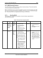
The National Semiconductor* PC87417 Super I/O provides nine general-purpose input/output
pins that the SE7501WV2 server board utilizes. The following table identifies the pin and the
signal name used in the schematic:
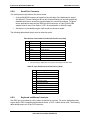
Table 6. Super I/O GPIO Usage Table
Pin
124
Name
GPIO00/CLKRUN_L
IO/GPIO
I/O
Intel® Server Board
SE7501WV2 Use
TP
125
GPIO01/KBCLK
I/O
KB_CLK
126
GPIO02/KBDAT
I/O
KB_DAT
127
GPIO03/MCLK
I/O
MS_CLK
128
GPIO04/MDAT
I/O
MS_DAT
9
GPIO05/XRDY
I/O
TP
10
GPIO06/XIRQ
I/O
BMC_SYSIRQ
13
GPIO07/HFCKOUT
I/O
SIO_CLK_40M_BMC
1
GPIOE10/XA11
I/O,I(E)1
XBUS_A<11>
2
GPIOE11/XA10
I/O,I(E)1
XBUS_A<10>
3
GPIOE12/XA9
I/O,I(E)1
XBUS_A<9>
4
GPIOE13/XA8
I/O,I(E)1
XBUS_A<8>
5
GPIOE14/XA7
I/O,I(E)1
XBUS_A<7>
6
GPIOE15/XA6
I/O,I(E)1
XBUS_A<6>
7
GPIOE16/XA5
I/O,I(E)1
XBUS_A<5>
Revision 1.0
32
Intel reference number C25653-001
Intel® Server Board SE7501WV2 TPS
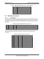
3.3.2
Functional Architecture
Pin
8
Name
GPIOE17/XA4
IO/GPIO
I/O,I(E)1
Intel® Server Board
SE7501WV2 Use
XBUS_A<4>
14
GPIO20/XRD_XEN_L
I/O
XBUS_XRD_L
15
GPIO21/XWR_XRW_L
I/O
XBUS_XWR_L
16
GPIO22/XA3
I/O
XBUS_A<3>
17
GPIO23/XA2
I/O
XBUS_A<2>
18
GPIO24/XA1
I/O
XBUS_A<1>
19
GPIO25/XA0
I/O
XBUS_A<0>
22
GPIO26/XCS1_L
I/O
TP
23
GPIO27/XCS0_L
I/O
XBUS_XCS0_L
24
GPIO30/XD7
I/O
XBUS_D<7>
25
GPIO31/XD6
I/O
XBUS_D<6>
26
GPIO32/XD5
I/O
XBUS_D<5>
27
GPIO33/XD4
I/O
XBUS_D<4>
28
GPIO34/XD3
I/O
XBUS_D<3>
29
GPIO35/XD2
I/O
XBUS_D<2>
30
GPIO36/XD1
I/O
XBUS_D<1>
31
GPIO37/XD0
I/O
XBUS_D<0>
20
GPIOE40/XCS3_L
I/O,I(E)1
TP
21
GPIOE41/XCS2_L
I/O,I(E)1
TP
35
GPIOE42/SLBTIN_L
I/O,I(E)1
TP
49
GPIOE43/PWBTOUT_L
I/O,I(E)1
ZZ_POST_CLK_LED_L
50
GPIOE44/LED1
I/O,I(E)1
ZZ_BIOS_ROLLING
51
GPIOE45/LED2
I/O,I(E)1
FP_PWR_LED_L
52
GPIOE46/SLPS3_L
I/O,I(E)1
TP
53
GPIOE47/SLPS5_L
I/O,I(E)1
TP
36
GPIO50/PWBTN_L
I/O
TP
37
GPIO51/SIOSMI_L
I/O
TP
38
GPIO52/SIOSCI_L
I/O
SIO_PME_L
45
GPIO53/LFCKOUT/MSEN0
I/O
TP
54
GPIO54/VDDFELL
I/O
ZZ_POST_DATA_LED_L
56
GPIO55/CLKIN
I/O
CLK_48M_SIO
32
GPO60/XSTB2/XCNF2_L
O
PU_XBUS_XCNF2
33
GPO61/XSTB1/XCNF1_L
O
XBUS_XSTB1_L
34
GPO62/XSTB0/XCNF0_L
O
PU_XBUS_XCNF0
48
GPO63/ACBSA
O
PU_SIO_ACBSA
55
GPO64/WDO_L/CKIN48
O
PU_SIO_CKIN48
Serial Ports
The SE7501WV2 server board provides two serial ports: an external low-profile RJ45 Serial
port, and an internal Serial header. The following sections provide details on the use of the
serial ports.
Revision 1.0
33
Intel reference number C25653-001
Functional Architecture
3.3.2.1
Intel® Server Board SE7501WV2 TPS
Serial Port A
Serial A is an optional port, accessed through a 9-pin internal header (J9A2). A standard DH-10
to DB9 cable can be used to direct Serial A out the back of a given chassis. The Serial A
interface follows the standard RS232 pin-out. The baseboard has a Serial Port A silkscreen
label next to the connector as well as a location designator of J9A2. The Serial A connector is
located next to the P64-C low-profile PCI card slot. A standard DH-10 to DB9 cable is available
from Intel Corporation in the SE7501WV2 Serial Port Accessory Kit.
Table 7. Serial A Header Pin-out
Pin
3.3.2.2
Signal Name
1
DCD
2
DSR
3
RX
4
RTS
5
TX
6
CTS
7
DTR
8
RI
9
GND
Serial Port A Header Pin-out
Serial Port B
Serial B is an external low profile 8-pin RJ45 connector that is located on the back of the board.
For those server applications that require an external modem, an RJ45-to-DB9 adapter is
necessary. A standard DH-10 to DB9 cable is available from Intel in the SE7501WV2 Serial Port
Accessory Kit.
3.3.2.3
Serial Port Multiplexer Logic
The SE7501WV2 server board has a multiplexer to connect the rear RJ45 connector to either
Serial Port A or Serial Port B in both the Intel® Server Chassis SR1300 and SR2300. This
facilitates the routing of Serial Port A to the rear RJ45 connector if Serial Port B is used for SOL
(Serial Over LAN) in both the SR1300 and SR2300 server chassis. This serial port selection can
be done through the BIOS setup option.
The following figure shows the serial port mux functionality.
Revision 1.0
34
Intel reference number C25653-001
Intel® Server Board SE7501WV2 TPS
Functional Architecture
Serial B
SIO
Bus
Exchange
Serial A
BMC
2 to 1
Mux
Level
Shifter
Level
shifter
Header
Rear
RJ45
Figure 4. Serial Port Mux Logic
3.3.2.3.1
Rear RJ45 Serial B Port
The rear RJ45 Serial B port is a fully functional serial port that can support any standard serial
device. Using an RJ45 connector for a serial port allows direct support for serial port
concentrators, which typically use RJ45 connectors and are widely used in the high-density
server market. For server applications that use a serial concentrator to access the server
management features of the baseboard, a standard 8-pin CAT-5 cable from the serial
concentrator is plugged directly into the rear RJ45 serial port.
To allow support of either of two serial port configuration standards used by serial port
concentrators, the J5A2 jumper block located directly behind the rear RJ45 serial port must be
jumpered appropriately according to the desired standard.
Note: By default as configured in the factory, the SE7501WV2 baseboard will have the rear
RJ45 serial port configured to support a DSR signal which is compatible with the Cisco*
standard.
For serial concentrators that require a DCD signal, the J5A2 jumper block must be configured
as follows: The Serial Port jumper placed in position 1 and 2. Pin 1 on the jumper is denoted by
an arrow directly next to the jumper block. The following diagram provides the jumper block pinout for this configuration.
Revision 1.0
35
Intel reference number C25653-001
Functional Architecture
Intel® Server Board SE7501WV2 TPS
PIN 1
Pin 1 – DCD to Pin #7
Figure 5. J5A2 Jumper Block for DCD Signal
For serial concentrators that require a DSR signal (Default), the J5A2 jumper block must be
configured as follows: The Serial Port jumper in position 3 and 4. Pin 1 on the jumper is
denoted by an arrow directly next to the jumper block.
PIN 1
Pin 1 - DSR to Pin#7
Figure 6. J5A2 Jumper Block for DSR Signal
For those server applications that require a DB9 serial connector, an 8-pin RJ45-to-DB9 adapter
must be used. The following table provides the pin-out required for the adapter to provide
RS232 support. A standard DH-10 to DB 9 cable and 8-pin RJ45 to DB9 DCD & DSR adapters
are available from Intel in the Serial Accessory Kit.
Table 8. Rear Serial Port B Adapter Pinout
RJ45
1
Signal
Request to Send
Abbr.
RTS
DB9
7
2
Data Terminal Ready
DTR
4
3
Transmitted Data
TD
3
4
Signal Ground
SGND
5
5
Ring Indicator
RI
9
6
Received Data
RD
2
7
DCD or DSR
DCD/DSR
1 or 6*
8
Clear To Send
CTS
8
Note: The RJ45-to-DB9 adapter should match the configuration of the serial device used. One
of two pin-out configurations is used depending on whether the serial device requires a DSR or
DCD signal. The final adapter configuration should also match the desired pin-out of the RJ45
connector, as it can also be configured to support either DSR or DCD.
Revision 1.0
36
Intel reference number C25653-001
Intel® Server Board SE7501WV2 TPS
Functional Architecture
For example, Modem applications typically use a DCD signal. In this case the user would use a
DCD-configured adapter and set the jumper block as shown in Figure 5.
3.3.2.4
Floppy Disk Controller
The floppy disk controller (FDC) in the SIO is functionally compatible with floppy disk controllers
in the DP8473 and N844077. All FDC functions are integrated into the SIO including analog
data separator and 16-byte FIFO. The SE7501WV2 server board provides two separate
interfaces for the floppy disk controller. The first is a SSI compliant 36-pin connector, and the
second is through the high-density 100-pin floppy / front panel / IDE connector.
Note: Using both interfaces in a common configuration is not supported.
3.3.2.5
Keyboard and Mouse
One external PS/2 port located on the back of the baseboard is provided for either a keyboard
or a mouse. A PS/2 Y-cable can be used to provide simultaneous support for both a keyboard
and mouse.
3.3.2.6
Wake-up Control
The Super I/O contains functionality that allows various events to control the power-on and
power-off the system.
3.3.3
BIOS Flash
The SE7501WV2 server board incorporates an Intel® 3 Volt Advanced+ Boot Block 28F320C3
Flash memory component. The 28F320C3 is a high-performance 32-megabit memory
component that provides 2048K x 16 of BIOS and non-volatile storage space. The flash device
is connected through the X-bus from the SIO.
Revision 1.0
37
Intel reference number C25653-001
Configuration and Initialization
4.
Intel® Server Board SE7501WV2 TPS
Configuration and Initialization
This section describes the configuration and initialization of various baseboard sub-systems as
implemented on the SE7501WV2 server board.
4.1.1
Main Memory
All installed memory greater than 1 MB is mapped to local main memory, up to the top of
physical memory, which is located at 12 GB. Memory between 1 MB to 15 MB is considered
standard ISA extended memory. 1 MB of memory starting at 15 MB can be optionally mapped
to the PCI bus memory space.
The remainder of this space, up to 12 GB, is always mapped to main memory, unless Extended
SMRAM is used, which limits the top of memory to 256 MB.
4.1.1.1
PCI Memory Space
Memory addresses below the 4 GB range are mapped to the PCI bus. This region is divided into
three sections: High BIOS, APIC Configuration Space, and General-purpose PCI Memory. The
General-purpose PCI Memory area is typically used for memory-mapped I/O to PCI devices.
The memory address space for each device is set using PCI configuration registers.
4.1.1.2
High BIOS
The top 2 MB of Extended Memory is reserved for the system BIOS, extended BIOS for PCI
devices, and A20 aliasing by the system BIOS. The Intel® Xeon™ processor begins executing
from the high BIOS region after reset.
4.1.1.3
I/O APIC Configuration Space
A 64 KB block located 20 MB below 4 GB is reserved for the I/O APIC configuration space.
4.1.1.4
Extended Xeon Processor Region (above 4GB)
®
An Intel Xeon™ processor-based system can have up to 64 GB of addressable memory. The
BIOS uses the Extended Addressing mechanism to use the address ranges.
4.1.2
Memory Shadowing
Any block of memory that can be designated as read-only or write-only can be “shadowed” into
main memory. This is typically done to allow ROM code to execute more rapidly out of RAM.
ROM is designated read-only during the copy process while RAM at the same address is
designated write-only. After copying, the RAM is designated read-only and the ROM is
designated write-only (shadowed). Processor bus transactions are routed accordingly.
Transactions originated from the PCI bus or ISA masters and targeted at the shadowed memory
block will not appear on the processor’s bus.
Revision 1.0
38
Intel reference number C25653-001
Intel® Server Board SE7501WV2 TPS
4.1.3
Configuration and Initialization
System Management Mode Handling
®
The Intel E7501 MCH supports System Management Mode (SMM) operation in standard
(compatible) mode. System Management RAM (SMRAM) provides code and data storage
space for the SMI_L handler code, and is made visible to the processor only on entry to SMM,
or other conditions, which can be configured using Intel E7501 PCI registers.
4.2
I/O Map
The SE7501WV2 allows I/O addresses to be mapped to the processor bus or through
designated bridges in a multi-bridge system. Other PCI devices, including the ICH3-S, have
built-in features that support PC-compatible I/O devices and functions, which are mapped to
specific addresses in I/O space. On the SE7501WV2 server board, the ICH3-S provides the
bridge to ISA functions through the LPC bus.
4.3
Accessing Configuration Space
All PCI devices contain PCI configuration space, accessed using mechanism #1 defined in the
PCI Local Bus Specification.
If dual processors are used, only the processor designated as the Boot-strap Processor (BSP)
should perform PCI configuration space accesses. Precautions should be taken to guarantee
that only one processor performs system configuration.
When CONFIG_ADDRESS is written to with a 32-bit value (selecting the bus number, device on
the bus, and specific configuration register in the device), a subsequent read or write of
CONFIG_DATA initiates the data transfer to/from the selected configuration register. Byte
enables are valid during accesses to CONFIG_DATA; they determine whether the configuration
register is being accessed or not. Only full Dword reads and writes to CONFIG_ADDRESS are
recognized as a configuration access by the Intel chipset. All other I/O accesses to
CONFIG_ADDRESS are treated as normal I/O transactions.
4.3.1
CONFIG_ADDRESS Register
CONFIG_ADDRESS is 32 bits wide and contains the field format shown in the following figure.
Bits [23::16] choose a specific bus in the system. Bits [15::11] choose a specific device on the
selected bus. Bits [10:8] choose a specific function in a multi-function device. Bit [8::2] select a
specific register in the configuration space of the selected device or function on the bus.
Revision 1.0
39
Intel reference number C25653-001
Configuration and Initialization
31 30
Intel® Server Board SE7501WV2 TPS
24 23
Reserved
16 15
Bus Number
11 10
Device
8 7
Functio
1 0
Register
0 0
Enable bit (‘1’ = enabled, ‘0’ = disabled)
Figure 7. CONFIG_ADDRES Register
4.3.1.1
Bus Number
PCI configuration space protocol requires that all PCI buses in a system be assigned a bus
number. Furthermore, bus numbers must be assigned in ascending order within hierarchical
buses. Each PCI bridge has registers containing its PCI bus number and subordinate PCI bus
number, which must be loaded by POST code. The Subordinate PCI bus number is the bus
number of the last hierarchical PCI bus under the current bridge. The PCI bus number and the
Subordinate PCI bus number are the same in the last hierarchical bridge.
4.3.1.2
Device Number and IDSEL Mapping
Each device under a PCI bridge has its IDSEL input connected to one bit out of the PCI bus
address/data signals AD[31::11] for the PCI bus. Each IDSEL-mapped AD bit acts as a chip
select for each device on PCI. The host bridge responds to a unique PCI device ID value, that
along with the bus number, cause the assertion of IDSEL for a particular device during
configuration cycles. The following table shows the correspondence between IDSEL values and
PCI device numbers for the PCI bus. The lower 5-bits of the device number are used in
CONFIG_ADDRESS bits [15::11].
Table 9. PCIdevice IDs
Device Description
Bus
North Bridge (MCH)
0
Device ID
(Hex)
00
ICH3 P2P Bridge
1
1E
ICH3 USB
1
1D
ICH3 IDE
1
1F
Video
1
0C
RIDE
1
02
Revision 1.0
40
Intel reference number C25653-001
Intel® Server Board SE7501WV2 TPS
Device Description
4.4
Configuration and Initialization
Bus
Device ID
(Hex)
0A
RMC Connector
1
P64H2 P2P Bridge A
2
1F
P64H2 P2P Bridge B
2
1D
Dual Gigabit NIC
3
07
PCI Slot 1B
3
08
PCI Slot 2B
3
09
PCI Slot 3B
3
0A
SCSI
4
07
PCI Slot 1C
4
08
PCI Slot 2C
4
09
PCI Slot 3C
4
0A
Hardware Initialization
An Intel® Xeon™ processor system based on Intel E7501 MCH is initialized in the following
manner.
1. When power is applied, after receiving RST_PWRGD_PS from the power supply, the
BMC provides resets using the RST_P6_PWRGOOD signal. The ICH3-S asserts
PCIRST_L to MCH, P64H2, and other PCI devices. The MCH then asserts
RST_CPURST_L to reset the processor(s).
2. The MCH is initialized, with its internal registers set to default values. Before
RST_CPURST_L is deasserted, the MCH asserts BREQ0_L. Processor(s) in the system
determine which host bus agents they are, Agent 0 or Agent 3, based on whether their
BREQ0_L or BREQ1_L is asserted. This determines bus arbitration priority and order.
3. After the processor(s) in the system determines which processor will be the BSP, the
non-BSP processor becomes an application processor and idles, waiting for a Startup
Inter Processor Interrupt (SIPI).
4. The BSP begins by fetching the first instruction from the reset vector.
5. The Intel® E7501 chipset registers are updated to reflect memory configuration. DIMM is
sized and initialized.
6. All PCI and ISA I/O subsystems are initialized and prepared for booting.
Refer to the SE7501WV2 BIOS EPS for more details regarding system initialization and
configuration.
4.5
Clock Generation and Distribution
All buses on the SE7501WV2 baseboard operate using synchronous clocks. Clock
synthesizer/driver circuitry on the baseboard generates clock frequencies and voltage levels as
required, including the following:
Revision 1.0
41
Intel reference number C25653-001
Configuration and Initialization
Intel® Server Board SE7501WV2 TPS
•
•
•
100 MHz differentials: For INT3/FCPGA sockets, the MCH, and the ITP port.
66 MHz at 3.3 V logic levels: For MCH, P64H2, ICH3, and IDE RAID Controller clock
33.3 MHz at 3.3 V logic levels: Reference clock for ICH3, BMC, Video, SIO, and the IDE
RAID controllers
• 48MHz: ICH3-S, and SIO
• 14.318 MHz at 3.3V logic levels: ICH3-S, and video clocks
For information on processor clock generation, see the CK408B Synthesizer/Driver Specification.
The SE7501WV2 baseboard also provides asynchronous clock generators:
•
•
80-MHz clock for the embedded SCSI controller
25-MHz clock for the embedded Network Interface controllers
• 32-KHz clock for the ICH3-S RTC
The following figure illustrates clock generation and distribution on the SE7501WV2 server
board.
Revision 1.0
42
Intel reference number C25653-001
Intel® Server Board SE7501WV2 TPS
Configuration and Initialization
Figure 8. Intel® Server Board SE7501WV2 Clock Distribution
Revision 1.0
43
Intel reference number C25653-001
Configuration and Initialization
4.6
Intel® Server Board SE7501WV2 TPS
PCI I/O Subsystem
4.6.1
PCI Subsystem
The primary I/O bus for the SE7501WV2 server board is the PCI subsystem, with three
independent PCI bus segments. The PCI bus complies with the PCI Local Bus Specification,
Rev 2.2. The P32-A bus segment is directed through the ICH South Bridge while the two 64-bit
segments, P64-B and P64-C, are directed through the P64H2 I/O Bridge. The following table
lists the characteristics of the three PCI bus segments.
Table 10. PCI Bus Segment Characteristics
PCI Bus
Segment
Voltage
Width
P32-A
5V
32-bits
PCI 33 MHz
Peer Bus
–
P64-B
3V
64-bits
PCI-X 100 MHz
Peer Bus
Supports full-length cards, 3.3V bus
P64-C
3V
64-bits
PCI-X 100 MHz
Peer Bus
Supports low-profile cards, 3.3V bus
4.6.2
Speed
Type
PCI I/O Riser Slots
P32-A: 32-bit, 33-MHz PCI Subsystem
All 32-bit, 33-MHz PCI I/O for the SE7501WV2 server board is directed through the ICH South
Bridge. The 32-bit, 33-MHz PCI segment created by the ICH is known as the P32-A segment.
The P32-A segment supports the following embedded devices and connectors:
•
•
2D/3D Graphics Accelerator: ATI Rage* XL Video Controller
ATA-100 controller: Promise Technology* PDC20277
Each of the embedded devices listed above can be disabled via a BIOS Setup option.
4.6.2.1
Device IDs (IDSEL)
Each device under the PCI hub bridge has its IDSEL signal connected to one bit of AD[31:16],
which acts as a chip select on the PCI bus segment in configuration cycles. This determines a
unique PCI device ID value for use in configuration cycles. The following table shows the bit to
which each IDSEL signal is attached for P32-A devices and the corresponding device description.
Table 11. P32-A Configuration IDs
IDSEL Value
4.6.2.2
Device
28
ATI Rage XL Video Controller
18
ATA-100 controller Promise Technology PDC20277
P32-A Arbitration
P32-A supports three PCI masters (ATA Rage XL, Promise ATA-100 Controller, and the ICH3S). All PCI masters must arbitrate for PCI access, using resources supplied by the ICH. The
Revision 1.0
44
Intel reference number C25653-001
Intel® Server Board SE7501WV2 TPS
Configuration and Initialization
host bridge PCI interface (ICH) arbitration lines REQx* and GNTx* are special cases in that they
are internal to the host bridge. The following table defines the arbitration connections.
Table 12. P32-Arbitration Connections
Baseboard Signals
4.6.3
Device
P32_REQ4*/P32_GNT1*
Promise ATA-100 Controller ( ATA Version Only)
P32_REQ0*/P32_GNT0*
ATA Rage XL video controller
P64-B and P64-C: 64-bit, 100-MHz PCI-X Subsystem
There are two peer 64-bit, 100-MHz PCI-X bus segments directed through the P64H2 I/O
Bridge.
The first PCI-X segment, P64-B, provides a single I/O Riser slot capable of supporting full
length, full height PCI cards. The PCI cards must meet the PCI specification for height, inclusive
of cable connections and memory. In addition to the riser connector, the P64-B segment also
has an Intel® 82546EB dual channel Gigabit Ethernet controller.
The second PCI-X segment, P64-C, provides a second I/O riser slot. Because of physical
limitations of the baseboard, this riser slot is only capable of supporting low-profile PCI cards. In
addition to the riser connector, the P64-C segment also has an Adaptec* 7902 dual channel U320 SCSI controller.
4.6.3.1
Device IDs (IDSEL)
Each device under the PCI hub bridge has its IDSEL signal connected to one bit of AD[31:16],
which acts as a chip select on the PCI bus segment in configuration cycles. This determines a
unique PCI device ID value for use in configuration cycles. The following tables show the bit to
which each IDSEL signal is attached for P64-B and P64-C devices, and corresponding device
description.
Table 13. P64-B Configuration IDs
IDSEL Value
23
Device
On-board Gigabit Ethernet controller
24
First slot of the riser card
25
Second slot of the riser card ( for a 3-slot riser card)
26
Third slot of the riser card (for a 3-slot riser card)
Table 14. P64-C Configuration IDsIDs
IDSEL Value
Device
Revision 1.0
45
Intel reference number C25653-001
Configuration and Initialization
4.6.3.2
Intel® Server Board SE7501WV2 TPS
23
On-board U320 SCSI controller
24
First slot of the riser card
25
Second slot of the riser card (for a 3-slot riser card)
26
Third slot of the riser card (for a 3-slot riser card)
P64-B Arbitration
The P64-B supports five PCI masters (the on-board gigabit ethernet controller, three slots on
the 3-slot PCI Riser, and the P64H2). All PCI masters must arbitrate for PCI access using
resources supplied by the P64H2. The host bridge PCI interface (P64H2) arbitration lines
REQx* and GNTx* are special cases in that they are internal to the host bridge. The following
table defines the arbitration connections.
Table 15. P64-B Arbitration Connections
P64H2 Signals
4.6.3.3
Device
P_REQ1*/P_GNT1*
Embedded Ethernet controller
P_REQ2*/P_GNT2*
P64-B: Top slot of the 3-slot riser
P_REQ3*/P_GNT3*
P64-B: Middle slot of the 3-slot riser
P_REQ4*/P_GNT4*
P64-B: Bottom slot of the 3-slot riser
P64-C Arbitration
P64-C supports five PCI masters (three slots on the 3-slot PCI riser, the embedded U-320 SCSI
controller, and the P64H2). All PCI masters must arbitrate for PCI access, using resources
supplied by the P64H2. The host bridge PCI interface (P64H2) arbitration lines REQx* and
GNTx* are special cases in that they are internal to the host bridge. The following table defines
the arbitration connections.
Table 16. P64-C Arbitration Connections
P64H2 Signals
4.6.3.4
Device
S_REQ1*/S_GNT1*
Embedded U320 SCSI controller
S_REQ2*/S_GNT2*
P64-B: Top slot of the 3-slot riser
S_REQ3*/S_GNT3*
P64-B: Middle slot of the 3-slot riser
S_REQ4*/S_GNT4*
P64-B: Bottom slot of the 3-slot riser
Zero Channel RAID (ZCR) Capable Riser Slot
The SCSI version of the SE7501WV2 server board is capable of supporting the following zero
channel RAID controllers, the Intel® SRCZCR, SRCMRU and SRCMRX RAID Adapter and the
Adaptec* 2000S RAID adapter. ZCR cards are only supported in the first slot of the 3-slot PCI
riser cards or the 1-slot riser cards used on the P64-C PCI segment.
Revision 1.0
46
Intel reference number C25653-001
Intel® Server Board SE7501WV2 TPS
Configuration and Initialization
The ZCR add-in cards leverage the on-board SCSI controller along with their own built-in
intelligence to provide a complete RAID controller subsystem on-board. The riser card and
baseboard use an implementation commonly referred to as RAID I/O Steering (RAIDIOS)
specification version 0.92 to support this feature. If either of these supported RAID cards are
installed, then the SCSI interrupts are routed to the RAID adapter instead of to the PCI interrupt
controller. Also the IDSEL of the SCSI controller is not driven to the controller and thus will not
respond as an on-board device. The host-based I/O device is effectively hidden from the
system.
4.7
Ultra320 SCSI
The SCSI version of the SE7501WV2 server board provides an embedded dual-channel SCSI
bus through the use of the Adaptec* AIC-7902W SCSI controller, which is capable of supporting
up to 132 MB/sec SCSI transfers. The AIC-7902W controller contains two independent SCSI
controllers that share a single 64-bit, 100-MHz PCI-X bus master interface as a multifunction
device, packaged in a 456-pin BGA.
Internally, each controller is identical and is capable of operations using either 16-bit SE or LowVoltage Differential (LVD) SCSI providing 40 MBps (Ultra-wide SE), 80 MBps (Ultra 2), 160
MBps (Ultra 160/m) or 320 MBps (Ultra 320/M). Each controller has its own set of PCI
configuration registers and SCI I/O registers. The SE7501WV2 server board supports disabling
of the on-board SCSI controller through the BIOS Setup menu.
The SE7501WV2 server board provides active terminators, termination voltage, a re-settable
fuse, and a protection diode for both SCSI channels. By design, the on-board termination will
always be enabled. No ability will be provided to disable termination. Each of the two SCSI
channels has a connector interface. Channel A is an external high-density connector located on
the back of the board, and Channel B is a standard 68-pin internal connector.
The Adaptec* AIC-7902W SCSI controller adds a feature called Integrated SCSI
mirroring/striping also know as HostRAID1. Integrated SCSI mirroring/striping offers an entrylevel Raid functionality for reliable performance and fill data protection for storage systems.
HostRAID supports the following features:
• Boot array support
• Support for TAID 0 and DATA1 with Microsoft* Windows* operating systems
• RAID configuration and management utility in the system BIOS.
4.8
ATA-100
The ATA-100 version of the SE7501WV2 server board provides an embedded dual channel
ATA-100 bus through the use of the Promise Technology* PDC20277 ASIC. The PDC20277
ATA-100 controller contains two independent ATA-100 channels that share a single 32-bit, 33MHz PCI bus master interface as a multifunction device, packaged in a 128-pin PQFP.
The ATA-100 controller supports the following features:
1 For more details on Integrated SCSI mirroring/striping or HostRAID, see the Adaptec*
HostRAID User’s Guide.
Revision 1.0
47
Intel reference number C25653-001
Configuration and Initialization
•
•
•
•
•
Intel® Server Board SE7501WV2 TPS
A scatter/gather mechanism that supports both DMA and PIO IDE drives
Support for ATA proposal PIO Mode 0, 1, 2, 3, 4, DMA Mode 0, 1, 2, and Ultra DMA
Mode 0, 1, 2, 3, 4, 5
An IDE drive transfer rate capable of up to 100 MB/sec per channel
A host interface that complies with PCI Local Bus Specification, Revision 2.2
32-bit, 33-MHz bus speed and 132 MB/sec sustained transfer rate
The Promise* PDC20277 supports IDE RAID through dual ATA-100 Channels. In a RAID
configuration, multiple IDE hard drives are placed into one or more arrays of disks. Each array is
seen as an independent disk, though the array may include upwards of two, three, or four
drives. The IDE RAID can be configured as following:
•
•
•
•
RAID 0 – striping one to four drives
RAID 1 – mirroring two drives
RAID 1 + spare drive (three drives)
RAID 0 + one to four drives are required
RAID 0 configurations are used for high performance applications, as it doubles the sustained
transfer rate of its drives. RAID 1 configurations are primarily used for data protection to create
an identical drive backup to a secondary drive. Whenever a disk write is performed, the
controller sends data simultaneously to a second drive located on a different data channel. With
four drives attached to dual ATA-100 channels, two striped drive pairs can mirror each other
(RAID 0+1) for storage capacity and data redundancy.
4.9
Video Controller
The SE7501WV2 server board provides an ATI Rage XL PCI graphics accelerator, along with 8
MB of video DDR and support circuitry for an embedded SVGA video subsystem. The ATI Rage
XL chip contains a SVGA video controller, clock generator, 2D and 3D engine, and RAMDAC in
a 272-pin PBGA. One 2Mx32 SDRAM chip provides 8 MB of video memory.
The SVGA subsystem supports a variety of modes, up to 1600 x 1200 resolution in 8/16/24/32
bpp modes under 2D, and up to 1024 x 768 resolution in 8/16/24/32 bpp modes under 3D. It
also supports both CRT and LCD monitors up to a 100 Hz vertical refresh rate.
The SE7501WV2 server board provides a standard 15-pin VGA connector and supports
disabling of the on-board video through the BIOS setup menu or when a plug-in video card is
installed in any of the PCI slots.
4.9.1
Video Modes
The Rage XL chip supports all standard IBM VGA modes. The following table shows the 2D/3D
modes supported for both CRT and LCD.
Revision 1.0
48
Intel reference number C25653-001
Intel® Server Board SE7501WV2 TPS
Configuration and Initialization
Table 17. Video Modes
Intel® Server Board SE7501WV2 2D Video Mode Support
2D Mode
Refresh Rate (Hz)
8 bpp
16 bpp
24 bpp
32 bpp
640x480
60, 72, 75, 90, 100
Supported
Supported
Supported
Supported
800x600
60, 70, 75, 90, 100
Supported
Supported
Supported
Supported
1024x768
60, 72, 75, 90, 100
Supported
Supported
Supported
Supported
1280x1024
43, 60
Supported
Supported
Supported
Supported
1280x1024
70, 72
Supported
–
Supported
Supported
1600x1200
60, 66
Supported
Supported
Supported
Supported
1600x1200
76, 85
Supported
Supported
Supported
–
®
3D Mode
Refresh Rate (Hz)
Intel Server Board SE7501WV2 3D Video Mode Support with Z Buffer
Enabled
640x480
60,72,75,90,100
Supported
Supported
Supported
Supported
800x600
60,70,75,90,100
Supported
Supported
Supported
Supported
1024x768
60,72,75,90,100
Supported
Supported
Supported
Supported
1280x1024
43,60,70,72
Supported
Supported
–
–
Supported
–
–
–
1600x1200
60,66,76,85
3D Mode
Refresh Rate (Hz)
640x480
60,72,75,90,100
Supported
800x600
60,70,75,90,100
Supported
Supported
Supported
Supported
1024x768
60,72,75,90,100
Supported
Supported
Supported
Supported
Intel® Server Board SE7501WV2 3D Video Mode Support with Z Buffer
Disabled
Supported
Supported
Supported
1280x1024
43,60,70,72
Supported
Supported
Supported
–
1600x1200
60,66,76,85
Supported
Supported
–
–
4.9.2
Video Memory Interface
The memory controller subsystem of the Rage XL arbitrates requests from direct memory
interface, the VGA graphics controller, the drawing coprocessor, the display controller, the video
scalar, and the hardware cursor. Requests are serviced in a manner that ensures display
integrity and maximum CPU/coprocessor drawing performance.
The SE7501WV2 server board supports an 8MB (512Kx32bitx4 Banks) SDRAM device for
video memory. The following table shows the video memory interface signals.
Table 18. Video Memory Interface
Signal Name
CAS#
I/O Type
O
Description
Column Address Select
CKE
O
Clock Enable for Memory
CS#[1..0]
O
Chip Select for Memory
DQM[7..0]
O
Memory Data Byte Mask
DSF
O
Memory Special Function Enable
HCLK
O
Memory Clock
[11..0]
O
Memory Address Bus
Revision 1.0
49
Intel reference number C25653-001
Configuration and Initialization
4.9.3
Intel® Server Board SE7501WV2 TPS
MD[31..0]
I/O
Memory Data Bus
RAS#
O
Row Address Select
WE#
O
Write Enable
Front Panel Video Memory
When the SE7501WV2 server board is integrated into either a SR2300 or SR1300 chassis, the
SE7501WV2 supports video through the front panel or the rear I/O panel. This is accomplished
by routing video to two connectors. The rear video is provided through the standard DB15 video
connector located in the rear I/O panel. Video is routed to the front panel through the highdensity 100-pin connector.
Video is routed to the rear video connector by default. When a monitor is plugged into the front
panel video connector, video is routed to the front panel connector and the rear connector is
disabled. This can be done by “hot plugging” the video connector while the system is still
running.
4.10 Network Interface Controller (NIC)
The SE7501WV2 server board supports a dual-channel gigabit network interface controller
based on the Intel® 82546EB. The 82546EB is a highly integrated PCI LAN controller in a 21
mm2 PBGA package. The controller supports 10/100/1000 operation on both channels as well
as supports alert-on-LAN functionality. The SE7501WV2 server board supports independent
disabling of the two NIC controllers using the BIOS Setup menu.
The 82546EB supports the following features:
•
•
•
•
•
•
•
4.10.1
32-bit PCI/CarBus master interface
Integrated IEEE 802.3 10Base-T, 100Base-TX and 1000Base-TX compatible PHY
IEEE 820.3u auto-negotiation support
Full duplex support at 10 Mbps, 100Mbps and 1000 Mbps operation
Integrated UNDI ROM support
MDI/MDI-X and HWI support
Low power +3.3 V device
NIC Connector and Status LEDs
The 82546EB drives two LEDs located on each network interface connector. The link/activity
LED (to the left of the connector) indicates network connection when on, and Transmit/Receive
activity when blinking. The speed LED (to the right of the connector) indicates 1000-Mbps
operations when amber, 100-Mbps operations when green, and 10-Mbps when off.
4.11 Interrupt Routing
The SE7501WV2 server board interrupt architecture accommodates both PC-compatible PIC
mode and APIC mode interrupts through use of the integrated APICs in the ICH3-S and the
P64H2.
Revision 1.0
50
Intel reference number C25653-001
Intel® Server Board SE7501WV2 TPS
4.11.1
Configuration and Initialization
Legacy Interrupt Routing
For PC-compatible mode, the ICH3-S provides two 82C59-compatible interrupt controllers. The
two controllers are cascaded with interrupt levels 8-15 entering on level 2 of the primary
interrupt controller (standard PC configuration). A single interrupt signal is presented to the
processors, to which only one processor will respond for servicing.
4.11.1.1
Legacy Interrupt Sources
The following table recommends the logical interrupt mapping of interrupt sources on the
SE7501WV2 server board. The actual interrupt map is defined using configuration registers in the
ICH3-S.
Table 19. Interrupt Definitions
ISA Interrupt
INTR
Description
Processor interrupt.
NMI
NMI to processor.
IRQ1
Keyboard interrupt.
IRQ3
Serial port A or B interrupt from SIO device, user-configurable.
IRQ4
Serial port A or B interrupt from SIO device, user-configurable.
IRQ5
IRQ6
Floppy disk.
IRQ7
IRQ8_L
Active low RTC interrupt.
IRQ9
IRQ10
IRQ11
IRQ12
Mouse interrupt.
IRQ14
Compatibility IDE interrupt from primary channel IDE devices 0 and 1.
IRQ15
SMI*
System Management Interrupt. General purpose indicator sourced by the ICH3-S and BMC to the
processors.
SCI*
System Control Interrupt. Used by system to change sleep states and other system level type
functions.
4.11.2
Serialized IRQ Support
The SE7501WV2 server board supports a serialized interrupt delivery mechanism. Serialized
IRQs (SERIRQ) consist of a start frame, a minimum of 17 IRQ / data channels, and a stop
frame. Any slave device in the quiet mode may initiate the start frame. While in the continuous
mode, the start frame is initiated by the host controller.
4.11.3
APIC Interrupt Routing
For APIC mode, the SE7501WV2 server board interrupt architecture incorporates three Intel®
APIC devices to manage and broadcast interrupts to local APICs in each processor. One of the
APICs is located in the ICH3-S and the other two APICs are in the P64H2 (one for each PCI
Revision 1.0
51
Intel reference number C25653-001
Configuration and Initialization
Intel® Server Board SE7501WV2 TPS
bus). The I/O APICs monitor each interrupt on each PCI device including PCI. When an
interrupt occurs, a message corresponding to the interrupt is sent across the FSB processors.
The following table shows how the interrupts from the embedded devices and the PCI-X slots
are connected.
Table 20. Intel® Server Board SE7501WV2 Interrupt Mapping
IRQ
PCI Riser Connector
PCI Riser Slot 1
Device
PCI Riser Slot 2
PCI Riser Slot 3
IRQA
IRQB
IRQC
IRQD
IRQE
IRQF
IRQG
IRQH
IRQ14
IRQ15
SER IRQ
ICH3
P64H2 Ch A
Other
P64H2
Video
Promise ATA
Pri IDE
Sec IDE
SIO
IRQ0
LP INTA
LP INTA
IRQ1*
LP INTC
LP INTC
IRQ2*
LP INTD
LP INTD
IRQ3
LP INTB
LP INTB
LP INTD
LP INTC
SCSI INTB
SCSI INTA
LP INTA
LP INTD
IRQ4
LP TDO
LP INTB
LP INTA
IRQ5
LP TCK
LP INTC
LP INTB
IRQ6
IRQ7
IRQ8
IRQ9
IRQ10
IRQ11
IRQ12
IRQ13
IRQ14
IRQ15
P64H2 Ch B
IRQ1
FL INTC
FL INTC
IRQ2
FL INTD
FL INTD
IRQ3
FL INTB
FL INTB
FL INTA
FL INTD
IRQ4
FL TDO
FL INTB
FL INTA
IRQ5
FL TCK
FL INTC
FL INTB
IRQ6
Gigabit Ch A
IRQ7
Gigabit Ch B
IRQ8
IRQ9
IRQ10
IRQ11
Revision 1.0
52
Intel reference number C25653-001
Intel® Server Board SE7501WV2 TPS
Configuration and Initialization
IRQ12
IRQ13
IRQ14
IRQ15
Notes:
LP = Low Profile
FL = Full Length
Revision 1.0
53
Intel reference number C25653-001
Server Management
5.
Intel® Server Board SE7501WV2 TPS
Server Management
Network Activity LEDs
Power LED
System Identify LED
Drive Activity/Fault LED
Fault Status LED
Power Button
Reset Button
System Identify Button
Chassis Intrusion
Front Panel NMI Switch
The SE7501WV2 server management features are implemented using the Sahalee server
board management controller chip. The Sahalee BMC is an ASIC packaged in a 156-pin BGA
that contains a 32-bit RISC processor core and associated peripherals. The following diagram
illustrates the SE7501WV2 server management architecture.
FRU Replacement LEDs
FAN FRU LEDs are driven by the
baseboard, but the actual LEDs are
off-board, typically located near the
corresponding fans.
Front Panel Connectors
PROCESSOR SOCKETS
Aux. IPMB
Connector
NIC #2
NIC #1
COM1
'debug'
Header
Chip Set
COMM MUX
BBD COM1
BBD COM2
PCI PME
Private Management Busses
COM2
CPU Voltage (2)
CPU 'Core' Temp (2)
CPU Present (2)
ICMB
Transceiver
Header
COM 2
Thermal Trip (2)
(6)
Hot-swap
Backplane
Header
EMP
RI (W ake-on-Ring)
IERR (2)
(2)
DIMM SPD (6)
INTELLIGENT PLATFORM
MANAGEMENT BUS (IPMB)
GTL 1.25V
Baseboard
Temp 1
Temperature
Sensor
Logic 2.5V
ATA Board
(6)
FANs (6)
FAN Pack
Connector
FRU Info
(5)
Chassis
Intrusion
12V
BASEBOARD
MANAGEMENT
CONTROLLER
(BMC)
3.3V
-12V
3.3V Standby
LVDS-A Term. 1
LVDS-A Term. 2
LVDS-B Term. 1
LVDS-B Term. 2
To Power
Distribution
Board
Non-volatile, read-write storage
5V
Chip Set 1.2V
Power Connector
BASEBOARD
System I/F
PORTS
SMMBIOS
I/F
SYSTEM
EVENT
LOG
SENSOR
DATA
RECORDS
CODE
(updateable)
RAM
SMS
I/F
System Bus
Chip set NMIs
Chip set SMI
Platform
Management
Interrupt
Routing
FRU INFO
& CONFIG
DEFAULTS
- Chassis ID
- Baseboard ID
- Power State
NMI
SMI
Figure 9. Intel® Server Board SE7501WV2 Sahalee BMC Block Diagram
Revision 1.0
54
Intel reference number C25653-001
Intel® Server Board SE7501WV2 TPS
5.1
Server Management
Sahalee Baseboard Management Controller (BMC)
The Sahalee BMC contains a 32-bit RISC processor core and associated peripherals used to
monitor the system for critical events. The Sahalee BMC, packaged in a 156-pin BGA, monitors
all power supplies, including those generated by the external power supplies and those
regulated locally on the server board. The Sahalee BMC also monitors SCSI termination
voltage, fan tachometers for detecting a fan failure, and system temperature. Temperature is
measured on each of the processors and at locations on the server board away from the fans.
When any monitored parameter is outside of defined thresholds, the Sahalee BMC logs an
event in the system event log.
Management controllers and sensors communicate on the I2C*-based Intelligent Platform
Management Bus (IPMB). Attached to one of its private I2C bus is the Heceta5, an ADM1026
device, which is a versatile systems monitor ASIC. Some of its features include:
•
•
•
•
•
•
Analog measurement channels
Fan speed measurement channels
General-Purpose Logic I/O pins
Remote temperature measurement
On-chip temperature sensor
Chassis intrusion detect
The following table details the inputs/outputs of the Sahalee BMC as used in the SE7501WV2
server system.
Table 21. BMC Pinout
Pin #
Pin Name
Signal
D1
RST*
BMC_RST_DLY_L
Type/
Config
input
M7
XTAL2
TP_SAH_XTAL2
output
Unused
P8
XTAL1
CLK_40M_BMC
input
40MHz clock from SIO
+2.5v reference voltage from Heceta5
C3
VREF
VREF_A_BMC_2P5V
input
A3
A2D0
TP_BMC_16
input
B4
A2D1
TP_TIC2_A2D<1>
input
C4
A2D2
TP_BMC_15
input
A4
A2D3
TP_BMC_A2D<3>
input
Description
Delayed version of A/C power-on reset
signal from Heceta5
D5
A2D4
TP_BMC_A2D<4>
input
B5
A2D5
TP_BMC_A2D<5>
input
C5
A2D6
PV_TERMPWR_SCWB_SCALE
D
input
SCSI Wide B Terminator voltage monitor.
A5
A2D7
PV_TERMPWR_SCWA_SCALE
D
input
SCSI Wide A Terminator voltage monitor.
J13
XINT0
RST_PWRGD_PS
input
Power Good signal from power supply
K11
XINT1
ICH3_SLP_S5_L
input
Sleep S5 signal from chipset ICH3
K12
XINT2
ICH3_SLP_S1_L
input
Sleep S1 signal from ICH3.
K14
XINT3
ZZ_FRB3_TIMER_HALT_L
input
Revision 1.0
55
Intel reference number C25653-001
Server Management
Pin #
Intel® Server Board SE7501WV2 TPS
Pin Name
Signal
K13
XINT4
NIC1_SMBALERT_L
Type/
Config
input
Description
L14
XINT5
ICH3_SMI_BUFF_L
input
L12
XINT6
BMC_PCU12_PROCHOT_L
input
Prochot signal. Can be Polled or Interrupt
SMBus Alert Signal from NIC1 (82546EB)
TCO port
L13
XINT7
BMC_NMI_L
OD out/in
NMI signal, monitored or asserted by BMC
D4
LPCRST*
RST_PCIRST_L
input
Buffered ICH3 PCIRST
E2
LPCPD*
ICH3_SUS_STAT_L
input
Signal used to 3-state LPC outputs to
prevent leakage
B11
LSMI*
BMC_SCI_L
OD
output
SCI output signal
F4
LDRQ*
LPC_DRQ_L<0>
output
G2
SYSIRQ
IRQ_SIO_SERIRQ
output
F3
LFRAME*
LPC_FRAME_L
input
G1
LCLK
CLK_33M_BMC
input
F1
LAD0
LPC_AD<0>
bidir
F2
LAD1
LPC_AD<1>
bidir
E3
LAD2
LPC_AD<2>
bidir
Connected to SIO GPIO06/XIRQ input
E1
LAD3
LPC_AD<3>
bidir
G3
CS1*
BMC_SRAM_CE_L
output
Chip enable for external SRAM
H1
CS0*
BMC_CS0_L
output
Chip enable for BMC flash/ memory mapped
latch
M10
WE*
BMC_WE_L
output
Flash/SRAM write enable
N10
OE*
BMC_OE_L
output
Flash/SRAM output enable
M14
BW8*
BMC_SLP_BTN_L
OD
output
Sleep input to ICH3
M13
IOCHRDY
FP_RST_BTN_L
input
Reset button signal from front panel
N14
BALE
FP_NMI_BTN_L
input
NMI button signal from front panel
P13
MEMR*
FP_ID_BTN_L
input
System ID signal from front panel
N13
MEMW*
FP_SLP_BTN_L
input
Sleep button signal from front panel. For ref
chassis support. (Not supported)
M12
IOR*
BMC_SECURE_MODE_KB
input
Secure mode signal from SIO keyboard
controller (pin 12)
N12
IOW*
FP_PWR_BTN_L
input
Power button signal from front panel
P12
SBHE*
BMC_SBHE_L
OD
output
High byte enable to external SRAM and
flash
M11
CE2*
RST_VRM_DIS_L
TP output
Disables CPU VRM.
N11
CE1*
BMC_VID_BLANK_L
TP output
Disables Hsync and Vsync video buffers
P11
REG*
BMC_CLR_CMOS_L
TP output
Clear CMOS signal asserted by BMC.
L4
ADDR0
BMC_A<0>
output
P4
ADDR1
BMC_A<1>
output
M4
ADDR2
BMC_A<2>
output
N4
ADDR3
BMC_A<3>
output
P3
ADDR4
BMC_A<4>
output
P2
ADDR5
BMC_A<5>
output
N2
ADDR6
BMC_A<6>
output
N1
ADDR7
BMC_A<7>
output
Revision 1.0
56
Intel reference number C25653-001
Intel® Server Board SE7501WV2 TPS
Pin #
Pin Name
BMC_A<8>
Type/
Config
output
ADDR9
BMC_A<9>
output
ADDR10
BMC_A<10>
output
ADDR11
BMC_A<11>
output
M2
ADDR8
M3
L2
L3
Signal
Server Management
L1
ADDR12
BMC_A<12>
output
K4
ADDR13
BMC_A<13>
output
K2
ADDR14
BMC_A<14>
output
K3
ADDR15
BMC_A<15>
output
K1
ADDR16
BMC_A<16>
output
J2
ADDR17
BMC_A<17>
output
J3
ADDR18
BMC_A<18>
output
J1
ADDR19
BMC_A<19>
output
H4
ADDR20
BMC_A<20>
output
H2
ADDR21
BMC_A<21>
output
P10
DATA0
BMC_D<0>
bidir
L9
DATA1
BMC_D<1>
bidir
Description
Only used if a 16M flash part is populated,
then unstuff pdn
N9
DATA2
BMC_D<2>
bidir
M9
DATA3
BMC_D<3>
bidir
P9
DATA4
BMC_D<4>
bidir
L8
DATA5
BMC_D<5>
bidir
N8
DATA6
BMC_D<6>
bidir
P7
DATA7
BMC_D<7>
bidir
N7
DATA8
BMC_D<8>
bidir
M6
DATA9
BMC_D<9>
bidir
P6
DATA10
BMC_D<10>
bidir
N6
DATA11
BMC_D<11>
bidir
L5
DATA12
BMC_D<12>
bidir
M5
DATA13
BMC_D<13>
bidir
P5
DATA14
BMC_D<14>
bidir
N5
DATA15
BMC_D<15>
bidir
J14
BAUD
BMC_IRQ_SMI_L
OD
output
Need to connect to SMI capable pin at ICH3
J12
RI*
SPB_RI_L
input
Serial 2 ring indicate signal.
F14
DTR0*
SPB_DTR_L
output
Serial 2 DTR signal.
F12
DCD0*
SPB_DCD_L
input
Serial 2 DCD signal.
F13
CTS0*
SPB_CTS_L
input
Serial 2 CTS signal.
F11
RTS0*
SPB_RTS_L
output
Serial 2 RTS signal.
E12
RX0
SPB_SIN
input
Serial 2 serial input signal
E13
TX0
SPB_SOUT
output
Serial 2 serial output signal
J11
DTR1*
BMC_LATCH_OE_L
TP output
Enables output of expansion latch
H13
DCD1*
BMC_ICMB_RX
input
ICMB receive data interrupt signal (same as
ICMB serial input)
H14
CTS1*
NSI_BMC_FRC_UPDATE_L
input
Forces BMC to run from boot block code.
Revision 1.0
57
Intel reference number C25653-001
Server Management
Pin #
Intel® Server Board SE7501WV2 TPS
Pin Name
Signal
H12
RTS1*
BMC_ICMB_TX_ENB _L
Type/
Config
TP output
Description
G14
RX1
BMC_ICMB_RX
input
ICMB serial receive data
G13
TX1
BMC_ICMB_TX
output
ICMB serial send data
BMC speaker tone enable signal (for beeps)
ICMB transceiver enable signal, asserted by
BMC
A12
TIC1_OUT
BMC_SPKR_L
TP output
B12
TIC2_IN0
FAN_TACH1
input
A13
TIC2_IN1
FAN_TACH2
input
B13
TIC2_IN2
FAN_TACH3
input
B14
TIC2_IN3
FAN_TACH4
input
C13
TIC2_IN4
FAN_TACH5
input
C14
TIC2_IN5
FAN_TACH6
input
PWT fan, CPU1
D13
TIC2_IN6
FAN_TACH7
input
PWT fan, CPU2
D12
TIC2_IN7
BMC_CPU1_SKTOCC_L
input
Socket occupied signal from CPU1
D14
TIC3_0UT
BMC_CPU2_SKTOCC_L
input
Socket occupied signal from CPU2
E11
TIC4_IN
SIO_CLK_32K_RTC_BMC
input
32kHz clock signal from IHC3
C10
LED0
BSEL_EQUAL_L
input
XOR gate compares CPU’s BSEL: if equal,
XOR will output a LO. Otherwise HI
A10
LED1
ZZ_BMC_ROLLING_BIOS_L
TP output
ROLLING BIOS flash control pin
B10
LED2
ZZ_SPA_SWITCH_EN
TP output
Connects to serial port Mux logic allowing
SPA to route to back in 1U chassis with SOL
enabled
D11
LED3
BMC_PWR_BTN_L
TP output
Power button signal from BMC to ICH3
A11
LED4
BMC_PS_PWR_ON_L
TP output
Power On signal to power supply
C11
LED5
RST_P6_PWR_GOOD
TP output
Chipset power good/rst signal
A6
SDA0
IPMB_I2C_5VSB_SDA
bidir
IPMB I2C data
B6
SCL0
IPMB_I2C_5VSB_SCL
bidir
IPMB I2C clock
B7
SDA1
SMB_I2C_3VSB_SDA
bidir
SMB I2C Bus data
D7
SCL1
SMB_I2C_3VSB_SCL
bidir
SMB I2C Bus clock
C8
SDA2
PB1_I2C_5VSB_SDA
bidir
BMC Private I2C Bus 1 - data.
A7
SCL2
PB1_I2C_5VSB_SCL
bidir
BMC Private I2C Bus 1 - clock.
B8
SDA3
SERIAL_TO_LAN_L
TP output
Serial bus cross-bar enable for null modem
operation through BMC to LAN.
A8
SCL3
EMP_INUSE_L
input
This status signal from the front panel
indicates that something is plugged into
Serial 2 RJ45.
C9
SDA4
PB3_I2C_3V_SDA
bidir
BMC Private I2C Bus 3 - data
D9
SCL4
PB3_I2C_3V_SCL
bidir
BMC Private I2C Bus 3 - clock
B9
SDA5
PB4_I2C_3VSB_SDA
bidir
BMC Private I2C Bus 4 - data
A9
SCL5
PB4_I2C_3VSB_SCL
bidir
BMC Private I2C Bus 4 - clock
C1
TMS
BMC_TMS
input
Sahalee JTAG signal
D2
TCK
BMC_TCK
input
Sahalee JTAG signal
B2
TDI
BMC_TDI
input
Sahalee JTAG signal
B1
TDO
BMC_TDO
output
Sahalee JTAG signal
C2
TRST*
BMC_TRST_L
input
Sahalee JTAG signal
D3
TEST_MODE* PULLUP
input
Sahalee test mode signal, should be pulled
high.
Revision 1.0
58
Intel reference number C25653-001
Intel® Server Board SE7501WV2 TPS
Pin #
Pin Name
Signal
Server Management
D6
AVDD
SB5V
Type/
Config
pwr/gnd
M1
VDD5V
SB5V
pwr/gnd
E14
VDD5V
SB5V
pwr/gnd
E4
IOVCC
SB3V
pwr/gnd
N3
IOVCC
SB3V
pwr/gnd
L10
IOVCC
SB3V
pwr/gnd
G11
IOVCC
SB3V
pwr/gnd
D10
IOVCC
SB3V
pwr/gnd
H3
COREVCC
SB3V
pwr/gnd
M8
COREVCC
SB3V
pwr/gnd
G12
COREVCC
SB3V
pwr/gnd
C7
COREVCC
SB3V
pwr/gnd
B3
AVS
GND
pwr/gnd
A2
AVSUB
GND
pwr/gnd
J4
IOGND
GND
pwr/gnd
L6
IOGND
GND
pwr/gnd
L11
IOGND
GND
pwr/gnd
C12
IOGND
GND
pwr/gnd
C6
IOGND
GND
pwr/gnd
G4
COREGND
GND
pwr/gnd
L7
COREGND
GND
pwr/gnd
H11
COREGND
GND
pwr/gnd
D8
COREGND
GND
pwr/gnd
Description
An ADM1026 has been attached to the Private 1 I2C bus for monitoring the system temperature,
additional analog voltages, and the voltage identifications bits for both processors. The following
table describes these added signals. The ADM1026 device also provides a PWM (Pulse Width
Modulation) for fan speed control.
Revision 1.0
59
Intel reference number C25653-001
Server Management
Intel® Server Board SE7501WV2 TPS
Table 22. ADM1026 Input Definition
Pin #
Pin Name
Signal
1
GPIO9
BMC_CPU2_IERR_L
Type/
Config
input
Description
2
GPIO8
BMC_CPU1_IERR_L
input
3
FAN0/GPIO0
BMC_DIS_CPU1_L
output
4
FAN1/GPIO1
BMC_DIS_CPU1_L
output
5
FAN2/GPIO2
VID_CPU2<0>
input
6
FAN3/GPIO3
VID_CPU2<1>
input
7
VDD
VCC3
pwr/gnd/in
8
DGND
GND
pwr/gnd
9
FAN4/GPIO4
VID_CPU2<2>
input
10
FAN5/GPIO5
VID_CPU2<3>
input
11
FAN6/GPIO6
VID_CPU2<4>
input
12
FAN7/GPIO7
VID_CPU1<0>
input
13
SCL
PB1_I2C_5VSB_SCL
bidir
BMC Private I2C Bus 1 - clock
14
SDA
PB1_I2C_5VSB_SDA
bidir
BMC Private I2C Bus 1 - data
15
ADDR/NTESTOU
T
PD_HEC5_ADDR
input
I2C address selection signal - I2C addr = 0X58
16
CHS_INT
NSI_CHASSIS_INTRUSION input
Chassis intrusion signal
17
INT*
TP_HEC5_INT_L
output
This pin does not yet have a specified
connection.
18
PWM
FAN_PWM_CNTRL
output
Fan speed control signal
This is the IERR signal from CPU2
This is the IERR signal from CPU1
19
RESET_STBY*
RST_BMC_RST_L
output
AC PowerOn reset
20
RESET*
TP_HEC5_RESET_L
in/out
This pin does not yet have a specified
connection.
21
AGND
GND
pwr/gnd
22
STBY_VDD
P3V3_STBY
pwr/gnd/in
23
DAC
TP_HEC5_DAC
output
This pin does not yet have a specified
connection.
24
VREF
VREF_A_BMC_2P5V
output
Analog input reference to Sahalee
25
D1-/NTESTIN
ZZ_CPU1_THERMDC
output
26
D1+
ZZ_CPU1_THERMDA
input
27
D2-/AIN9
ZZ_CPU2_THERMDC
output
28
D2+/AIN8
ZZ_CPU2_THERMDA
input
29
VBAT
P2V5_NIC
input
Baseboard P2V5_NIC monitor
30
+5V
P5V
input
Baseboard P5V monitor
31
-12V
N12V
input
Baseboard N12V monitor
32
+12V
P12V
input
Baseboard P12V monitor
33
VCCP
P_VCCP
input
Baseboard P_VCCP monitor
34
AIN7
P1V2
input
Baseboard P1V2 monitor
35
AIN6
P1V25_VTT
input
Baseboard P1V25_VTT monitor
36
AIN5
P12V_VRM_SCALED
input
External attenuator=232/(232+1k)~0.19
37
AIN4
P1V8
input
Baseboard P1V8 monitor
Revision 1.0
60
Intel reference number C25653-001
Intel® Server Board SE7501WV2 TPS
Pin #
Pin Name
38
AIN3
Signal
P2V5
Server Management
Type/
Config
input
Description
Baseboard P2V5 monitor
39
AIN2
P5V_STBY_SCALED
input
External attenuator=1k/(1k+1k)=0.5
40
AIN1
P1V8_STBY
input
Baseboard P1V8_STBY monitor
41
AIN0
P3V3_VAUX
input
External attenuator=499k/(499+365~=0.58
42
THERM*/GPIO16
TP_HEC5_GPIO16
gpio
This pin does not yet have a specified
connection.
43
GPIO15
BMC_CPU2_THRMTRIP_L
input
Processor Thermal Trip signal from CPU2
44
GPIO14
BMC_CPU1_THRMTRIP_L
input
Processor Thermal Trip signal from CPU1
46
GPIO13
VID_CPU1<3>
input
45
GPIO12
VID_CPU1<4>
input
47
GPIO11
VID_CPU1<2>
input
48
GPIO10
VID_CPU1<1>
input
5.1.1
Fault Resilient Booting
The Sahalee BMC implements Fault Resilient Booting (FRB) levels 1, 2, and 3. If the default
bootstrap processor (BSP) fails to complete the boot process, FRB attempts to boot using an
alternate processor.
•
FRB level 1 is for recovery from a BIST failure detected during POST. This FRB
recovery is fully handled by BIOS code.
•
FRB level 2 is for recovery from a watchdog timeout during POST. The watchdog timer
for FRB level 2 detection is implemented in the Sahalee BMC.
•
FRB level 3 is for recovery from a watchdog timeout on hard reset or power-up. The
Sahalee BMC provides hardware functionality for this level of FRB.
5.1.1.1
FRB-1
In a multiprocessor system, the BIOS registers the application processors in the MP table and
the ACPI tables. When started by the BSP, if an AP fails to complete initialization within a
certain time, it is assumed nonfunctional. If the BIOS detects that an application processor has
failed BIST or is nonfunctional, it requests the BMC to disable that processor. The BMC then
generates a system reset while disabling the processor; the BIOS will not see the bad processor
in the next boot cycle. The failing AP is not listed in the MP table (refer to the Multi-Processor
Specification, Rev. 1.4), nor in the ACPI APIC tables, and is invisible to the operating system. If
the BIOS detects that the BSP has failed BIST, it sends a request to the BMC to disable the
present processor. If there is no alternate processor available, the BMC beeps the speaker and
halts the system. If BMC can find another processor, BSP ownership is transferred to that
processor via a system reset.
5.1.1.2
FRB-2
The second watchdog timer (FRB-2) in the BMC is set for approximately 6 minutes by BIOS and
is designed to guarantee that the system completes BIOS POST. The FRB-2 timer is enabled
before the FRB-3 timer is disabled to prevent any “unprotected” window of time.
Revision 1.0
61
Intel reference number C25653-001
Server Management
Intel® Server Board SE7501WV2 TPS
Near the end of POST, before the option ROMs are initialized, the BIOS disables the FRB-2
timer in the BMC. If the system contains more than 1 GB of memory and the user chooses to
test every DWORD of memory, the watchdog timer is disabled before the extended memory test
starts, because the memory test can take more than 6 minutes under this configuration. If the
system hangs during POST, the BIOS does not disable the timer in the BMC, which generates
an asynchronous system reset (ASR).
5.1.1.3
FRB-3
The first timer (FRB-3) starts counting down whenever the system comes out of hard reset,
which is usually about 5 seconds. If the BSP successfully resets and starts executing, the BIOS
disables the FRB-3 timer in the BMC by de-asserting the FRB3_TIMER_HLT* signal (GPIO)
and the system continues with the POST. If the timer expires because of the BSP’s failure to
fetch or execute BIOS code, the BMC resets the system and disables the failed processor. The
system continues to change the bootstrap processor until the BIOS POST gets past disabling
the FRB-3 timer in the BMC. The BMC sounds beep codes on the speaker, if it fails to find a
good processor. The process of cycling through all the processors is repeated upon system
reset or power cycle.
5.2
System Reset Control
Reset circuitry on the SE7501WV2 server board looks at resets from the front panel, ICH3-S,
ITP, and the processor subsystem to determine proper reset sequencing for all types of resets.
The reset logic is designed to accommodate several methods to reset the system, which can be
divided into the following categories:
• Power-up reset
• Hard reset
• Soft (programmed) reset
The following subsections describe each type of reset.
5.2.1
Power-up Reset
When the system is disconnected from AC power, all logic on the server board is powered off.
When a valid input (AC) voltage level is provided to the power supply, 5-volt standby power will
be applied to the server board. The baseboard has a 5-volt to 3.3-volt regulator to produce
3.3-volt standby voltage. A power monitor circuit on 3.3-volt standby will assert BMCRST_L,
causing the BMC to reset. The BMC is powered by 3.3-volt standby and monitors and controls
key events in the system related to reset and power control.
After the system is turned on, the power supply will assert the RST_PWRGD_PS signal after all
voltage levels in the system have reached valid levels. The BMC receives RST_PWRGD_PS and
after 500 ms asserts RST_P6_PWR_GOOD, which indicates to the processors and ICH3-S that
the power is stable. Upon RST_P6_PWR_GOOD assertion, the ICH3-S will toggle PCI reset.
5.2.2
Hard Reset
A hard reset can be initiated by resetting the system through the front panel switch. During the
reset, the Sahalee BMC de-asserts RST_P6_PWR_GOOD. After 500 ms, it is reasserted, and
the power-up reset sequence is completed.
The Sahalee BMC is not reset by a hard reset; it is only reset when AC power is applied to the
system.
Revision 1.0
62
Intel reference number C25653-001
Intel® Server Board SE7501WV2 TPS
5.2.3
Server Management
Soft Reset
A soft reset causes the processors to begin execution in a known state without flushing caches
or internal buffers. Soft resets can be generated by the keyboard controller located in the SIO,
by the ICH3-S, or by the operating system.
5.3
Intelligent Platform Management Buses (IPMB)
Management controllers (and sensors) communicate on the I2C-based Intelligent Platform
Management Bus. A bit protocol, defined by the I2C Bus Specification, and a byte-level protocol,
defined by the Intelligent Platform Management Bus Communications Protocol Specification,
provide an independent interconnect for all devices operating on this I2C bus.
The IPMB extends throughout the server board and system chassis. An added layer in the
protocol supports transactions between multiple servers on Inter-Chassis Management Bus
(ICMB) I2C segments.
The server board provides a 3-pin IPMB connector to support add-in cards with IPMB interface.
In addition to the “public” IPMB, the BMC also has three private I2C busses. The BMC is the
only master on the private busses. The following table lists all server board connections to the
Sahalee BMC private I2C busses.
Table 23. Intel® Server Board SE7501WV2 I2C Address Map
I2C Bus
PB1
PB3
PB4
5.4
I2C Addr
0x58
0x60
0x30
0x32
0x44
0x60
0xA0
0xA2
0xA4
0xA6
0xA8
0xAA
0xAC
0xAE
0xC4
0xD2
Device
Heceta5
SIO
CPU1 therm sensor
CPU2 therm sensor
ICH3
MCH
DIMM1
DIMM3
DIMM5
CPU1 SEEPROM
DIMM2
DIMM4
DIMM6
CPU2 SEEPROM
P64H2
CK408B
NIC
Inter Chassis Management Bus (ICMB)
The BMC on the SE7501WV2 server board has built in support for ICMB interface. An optional
ICMB card is required to use this feature because the ICMB transceivers are not provided on
the server board. A 5-pin ICMB connector on the SE7501WV2 board provides the interface to
the ICMB module.
Revision 1.0
63
Intel reference number C25653-001
Server Management
5.5
Intel® Server Board SE7501WV2 TPS
Error Reporting
This section documents the types of system bus error conditions monitored by the SE7501WV2
board set.
5.5.1
Error Sources and Types
One of the major requirements of server management is to correctly and consistently handle
system errors. System errors on the SE7501WV2, which can be disabled and enabled
individually, can be categorized as follows:
•
•
•
•
PCI bus errors
Processor bus errors
Memory single- and multi-bit errors
General Server Management sensors
On the SE7501WV2 platform, the general server management sensors are managed by the
Sahalee BMC.
5.5.2
PCI Bus Errors
The PCI bus defines two error pins, PERR# and SERR#, for reporting PCI parity errors and
system errors, respectively. In the case of PERR#, the PCI bus master has the option to retry
the offending transaction, or to report it using SERR#. All other PCI-related errors are reported
by SERR#. SERR# is routed to NMI if enabled by BIOS.
5.5.3
Intel® Xeon™ Processor Bus Errors
The MCH supports the data integrity features supported by the Xeon bus, including address,
request, and response parity. In addition, the MCH can generate BERR# on unrecoverable
errors detected on the processor bus. Unrecoverable errors are routed to an NMI by the BIOS.
5.5.4
Memory Bus Errors
The MCH is programmed to generate an SMI on single-bit or double-bit data errors in the
memory array if ECC memory is installed. The MCH performs the scrubbing. The SMI handler
records the error and the DIMM location to the system event log.
5.5.5
Fault and Status LEDs
The SE7501WV2 server board uses system fault/status LEDs in many areas of the board.
There are fault LEDs for the memory DIMMs, the fan headers, and the processors. There are
also status LEDs for 5-volt stand-by and system status indication. A blue LED is provided as a
system ID LED. When the error reporting system determines there is a problem with any device,
it will light the LED of the failing component. In the event of a power switch power down or loss
of AC, the status of all baseboard fault LEDs will be remembered and restored by BMC when
AC is restored. Fault LEDs will only be reset when a Front Panel Reset is performed with main
power available to the system or under control of an IPMI command.
Revision 1.0
64
Intel reference number C25653-001
Intel® Server Board SE7501WV2 TPS
5.5.5.1
Server Management
DIMM LEDs
One LED for each DIMM will be illuminated if that DIMM has an uncorrectable or multi-bit
memory ECC. These LEDs will maintain the same state across power switch power down or
loss of AC. These LED’s will only be reset when a Front Panel Reset is performed with main
power available to the system or under control of an IPMI command.
5.5.5.2
CPU LEDs
There is one LED for each CPU. This LED will be illuminated if the associated processor has
been disabled. These LEDs will maintain the same state across power switch power down or
loss of AC. These LED’s will only be reset when a Front Panel Reset is performed with main
power available to the system or under control of an IPMI command.
5.5.5.3
Fan LEDs
One LED is provided for each fan header. This LED will be illuminated if the associated fan fails.
These LEDs will maintain the same state across power switch power down or loss of AC. There
is a consolidated fan fail LED for the fans powered by the fan assembly header (J3J2). These
LED’s will only be reset when a Front Panel Reset is performed with main power available to the
system or under control of an IPMI command.
5.5.5.4
5VSB Status LED
One single-color LED is located next to the main power connector. This LED indicates the
presence of 5-volt stand-by when AC power is applied to the system. AC is applied to the
system as soon as the AC cord is plugged into the power supply.
5.5.5.5
System Status LED
The SE7501WV2 server board has a System Status LED, which can be found on the other side
of the baseboard notch from the PORT80 diagnostic LEDs located near the back edge of the
baseboard. This LED is tied to the front panel System Status LED and should reflect the same
system status. The LED is a multi colored LED. The following table describes what each state
signifies:
Table 24. System Status LEDs
LED
System Status
[ on standby
power ]
Color
Green
State
ON
Blink
Degraded
Amber
ON
Critical or Non-Recoverable Condition.
Blink
Non-Critical condition.
OFF
POST / System Stop.
Off
Description
Running / Normal operation
Revision 1.0
65
Intel reference number C25653-001
Server Management
5.5.5.5.1
Intel® Server Board SE7501WV2 TPS
System Status Indications
Critical Condition
A critical condition is any critical or non-recoverable threshold crossing associated with the
following events:
•
Temperature, Voltage, or Fan critical threshold crossing
•
Power Subsystem Failure. The BMC asserts this failure whenever it detects a power
control fault (e.g., the BMC detects that the system power is remaining ON even though
the BMC has de-asserted the signal to turn off power to the system).
A hot-swap backplane would use the Set Fault Indication command to indicate when one
or more of the drive fault status LEDs are asserted on the hot-swap backplane.
•
The system is unable to power up due to incorrectly installed processor(s), or processor
incompatibility.
•
Satellite controller sends a critical or non-recoverable state, via the Set Fault Indication
command to the BMC.
•
“Critical Event Logging” errors.
Non-Critical Condition
•
Temperature, Voltage, or Fan non-critical threshold crossing
•
Chassis Intrusion
•
Satellite controller sends a non-critical state, via the Set Fault Indication command, to
the BMC.
•
Set Fault Indication Command
Degraded Condition
•
Non-redundant power supply operation. This only applies when the BMC is configured
for a redundant power subsystem. The power unit configuration is configured via OEM
SDR records.
•
A processor is disabled by FRB or BIOS.
•
BIOS has disabled or mapped out some of the system memory.
5.5.5.6
ID LED
The Blue ID LED, located at the back edge of the baseboard near the speaker, is used to help
locate a given server platform requiring service when installed in a multi-system rack. The LED
is lit when the front panel ID button is pressed and it is turned off when the button is pressed
again. A user-defined interface can be developed to activate the ID LED remotely.
Revision 1.0
66
Intel reference number C25653-001
Intel® Server Board SE7501WV2 TPS
5.5.5.7
Server Management
POST Code Diagnostic LEDs
To help diagnose POST failures, a set of four bi-color diagnostic LEDs is located on the back
edge of the baseboard. Each of the four LEDs can have one of four states: Off, Green, Red, or
Amber. During the POST process, each light sequence represents a specific Port-80 POST
code. If a system should hang during POST, the diagnostic LEDs will present the last test
executed before the hang. When reading the lights, the LEDs should be observed from the back
of the system. The most significant bit (MSB) is the first LED on the left, and the least significant
bit (LSB) is the last LED on the right.
Table 25. Boot Block POST Progress Codes
Diagnostic LED
Decoder
G=Green, R=Red,
A=Amber
Hi
Description
Low
10h
Off
Off
Off
R
The NMI is disabled. Start Power-on delay. Initialization code checksum
verified.
11h
Off
Off
Off
A
Initialize the DMA controller, perform the keyboard controller BAT test, start
memory refresh, and enter 4 GB flat mode.
12h
Off
Off
G
R
Get start of initialization code and check BIOS header.
13h
Off
Off
G
A
Memory sizing.
14h
Off
G
Off
R
Test base 512K of memory. Return to real mode. Execute any OEM patches
and set up the stack.
15h
Off
G
Off
A
Pass control to the uncompressed code in shadow RAM. The initialization code
is copied to segment 0 and control will be transferred to segment 0.
16h
Off
G
G
R
Control is in segment 0. Verify the system BIOS checksum.
If the system BIOS checksum is bad, go to checkpoint code E0h.
Otherwise, going to checkpoint code D7h.
17h
Off
G
G
A
Pass control to the interface module.
18h
G
Off
Off
R
Decompress of the main system BIOS failed.
19h
G
Off
Off
A
Build the BIOS stack. Disable USB controller. Disable cache.
1Ah
G
Off
G
R
Uncompress the POST code module. Pass control to the POST code module.
1Bh
A
R
Off
R
Decompress the main system BIOS runtime code.
1Ch
A
R
Off
A
Pass control to the main system BIOS in shadow RAM.
E0h
R
R
R
Off
Start of recovery BIOS. Initialize interrupt vectors, system timer, DMA controller,
and interrupt controller.
E8h
A
R
R
Off
Initialize extra module if present.
E9h
A
R
R
G
Initialize floppy controller.
EAh
A
R
A
Off
Try to boot floppy diskette.
EBh
A
R
A
G
If floppy boot fails, intialize ATAPI hardware.
ECh
A
A
R
Off
Try booting from ATAPI CD-ROM drive.
EEh
A
A
A
Off
Jump to boot sector.
EFh
A
A
A
G
Disable ATAPI hardware.
20h
Off
Off
R
Off
Uncompress various BIOS Modules
22h
Off
Off
A
Off
Verify password Checksum
24h
Off
G
R
Off
Verify CMOS Checksum.
Revision 1.0
67
Intel reference number C25653-001
Server Management
Intel® Server Board SE7501WV2 TPS
Diagnostic LED
Decoder
G=Green, R=Red,
A=Amber
Hi
Description
Low
26h
Off
G
A
Off
Read Microcode updates from BIOS ROM.
28h
G
Off
R
Off
Initializing the processors. Set up processor registers. Select least featured
processor as the BSP.
2Ah
G
Off
A
Off
Go to Big Real Mode
2Ch
G
G
R
Off
Decompress INT13 module
2Eh
G
G
A
Off
Keyboard Controller Test: The keyboard controller input buffer is free. Next,
issuing the BAT command to the keyboard controller
30h
Off
Off
R
R
Keyboard/Mouse port swap, if needed
32h
Off
Off
A
R
Write Command Byte 8042: The initialization after the keyboard controller BAT
command test is done. The keyboard command byte will be written next.
34h
Off
G
R
R
Keyboard Init: The keyboard controller command byte is written. Next, issuing
the pin 23 and 24 blocking and unblocking commands
36h
Off
G
A
R
Disable and initialize 8259
38h
G
Off
R
R
Detect Configuration Mode, such as CMOS clear.
3Ah
G
Off
A
R
Chipset Initialization before CMOS initialization
3Ch
G
G
R
R
Init System Timer: The 8254 timer test is over. Starting the legacy memory
refresh test next.
3Eh
G
G
A
R
Check Refresh Toggle: The memory refresh line is toggling. Checking the 15
second on/off time next
40h
Off
R
Off
Off
Calculate CPU speed
42h
Off
R
G
Off
Init interrupt Vectors: Interrupt vector initialization is done.
44h
Off
A
Off
Off
Enable USB controller in chipset
46h
Off
A
G
Off
Initialize SMM handler. Initialize USB emulation.
48h
G
R
Off
Off
Validate NVRAM areas. Restore from backup if corrupted.
4Ah
G
R
G
Off
Load defaults in CMOS RAM if bad checksum or CMOS clear jumper is
detected.
4Ch
G
A
Off
Off
Validate date and time in RTC.
4Eh
G
A
G
Off
Determine number of micro code patches present
50h
Off
R
Off
R
Load Micro Code To All CPUs
52h
Off
R
G
R
Scan SMBIOS GPNV areas
54h
Off
A
Off
R
Early extended memory tests
56h
Off
A
G
R
Disable DMA
58h
G
R
Off
R
Disable video controller
5Ah
G
R
G
R
8254 Timer Test on Channel 2
5Ch
G
A
Off
R
Enable 8042. Enable timer and keyboard IRQs. Set Video Mode: Initialization
before setting the video mode is complete. Configuring the monochrome mode
and color mode settings next.
5Eh
G
A
G
R
Init PCI devices and motherboard devices. Pass control to video BIOS. Start
serial console redirection.
60h
Off
R
R
Off
Initialize memory test parameters
62h
Off
R
A
Off
Initialize AMI display manager Module. Initialize support code for headless
system if no video controller is detected.
64h
Off
A
R
Off
Start USB controllers in chipset
66h
Off
A
A
Off
Set up video parameters in BIOS data area.
Revision 1.0
68
Intel reference number C25653-001
Intel® Server Board SE7501WV2 TPS
Diagnostic LED
Decoder
G=Green, R=Red,
A=Amber
Hi
Server Management
Description
Low
68h
G
R
R
Off
Activate ADM: The display mode is set. Displaying the power-on message next.
6Ah
G
R
A
Off
Initialize language module. Display splash logo.
6Ch
G
A
R
Off
Display Sign on message, BIOS ID and processor information.
Detect USB devices
6Eh
G
A
A
Off
70h
Off
R
R
R
Reset IDE Controllers
72h
Off
R
A
R
Displaying bus initialization error messages.
74h
Off
A
R
R
Display Setup Message: The new cursor position has been read and saved.
Displaying the Hit Setup message next.
76h
Off
A
A
R
Ensure Timer Keyboard Interrupts are on.
78h
G
R
R
R
Extended background memory test start
7Ah
G
R
A
R
Disable parity and NMI reporting.
7Ch
G
A
R
R
Test 8237 DMA Controller: The DMA page register test passed. Performing the
DMA Controller 1 base register test next
7Eh
G
A
A
R
Init 8237 DMA Controller: The DMA controller 2 base register test passed.
Programming DMA controllers 1 and 2 next.
80h
R
Off
Off
Off
Enable Mouse and Keyboard: The keyboard test has started. Clearing the
output buffer and checking for stuck keys. Issuing the keyboard reset command
next
82h
R
Off
G
Off
Keyboard Interface Test: A keyboard reset error or stuck key was found. Issuing
the keyboard controller interface test command next.
84h
R
G
Off
Off
Check Stuck Key Enable Keyboard: The keyboard controller interface test
completed. Writing the command byte and initializing the circular buffer next.
86h
R
G
G
Off
Disable parity NMI: The command byte was written and global data initialization
has completed. Checking for a locked key next
88h
A
Off
Off
Off
Display USB devices
8Ah
A
Off
G
Off
Verify RAM Size: Checking for a memory size mismatch with CMOS RAM data
next
8Ch
A
G
Off
Off
Lock out PS/2 keyboard/mouse if unattended start is enabled.
8Eh
A
G
G
Off
Init Boot Devices: The adapter ROM had control and has now returned control
to BIOS POST. Performing any required processing after the option ROM
returned control.
90h
R
Off
Off
R
Display IDE mass storage devices.
92h
R
Off
G
R
Display USB mass storage devices.
94h
R
G
Off
R
Report the first set of POST Errors To Error Manager.
96h
R
G
G
R
Boot Password Check: The password was checked. Performing any required
programming before Setup next.
98h
A
Off
Off
R
Float Processor Initialize: Performing any required initialization before the
coprocessor test next.
9Ah
A
Off
G
R
Enable Interrupts 0,1,2: Checking the extended keyboard, keyboard ID, and
NUM Lock key next. Issuing the keyboard ID command next
9Ch
A
G
Off
R
Init FDD Devices. Report second set of POST errors To Error messager
9Eh
A
G
G
R
Extended background memory test end
A0h
R
Off
R
Off
Prepare And Run Setup: Error manager displays and logs POST errors. Waits
for user input for certain errors. Execute setup.
Revision 1.0
69
Intel reference number C25653-001
Server Management
Intel® Server Board SE7501WV2 TPS
Diagnostic LED
Decoder
G=Green, R=Red,
A=Amber
Hi
Description
Low
A2h
R
Off
A
Off
Set Base Expansion Memory Size
A4h
R
G
R
Off
Program chipset setup options, build ACPI Tables, build INT15h E820h table
A6h
R
G
A
Off
Set Display Mode
A8h
A
Off
R
Off
Build SMBIOS table and MP tables.
AAh
A
Off
A
Off
Clear video screen.
ACh
A
G
R
Off
Prepare USB controllers for operating system
AEh
A
G
A
Off
One Beep to indicate end of POST. No beep if silent boot is enabled.
000h
Off
Off
Off
Off
POST completed. Passing control to INT 19h boot loader next.
5.5.6
Temperature Sensors
The SE7501WV2 server board has the ability to measure system and board temperature from a
variety of sources. The first is located inside the Heceta chip (U6G1) and is used to measure
the baseboard temperature. In addition, diodes located inside each processor are used by the
SE7501WV2 to monitor temperature at the processors. When installed in either the Intel
SR1300 or SR2300 server chassis, the SE7501WV2 also uses a temperature sensor on the
front panel to measure ambient temperature and will boost the fans depending on the reading it
receives from these sensors.
Revision 1.0
70
Intel reference number C25653-001
Intel® Server Board SE7501WV2 TPS
6.
BIOS
BIOS
This section describes the BIOS-embedded software for the SE7501WV2 server board. This
section also describes BIOS support utilities that are required for system configuration (ROM
resident) and flash ROM update (not ROM resident). The BIOS contains standard PCcompatible basic input/output (I/O) services and standard Intel® server features.
The BIOS is implemented as firmware that resides in the flash ROM. Support for applicable
baseboard peripheral devices (SCSI, NIC, video adapters, etc.) that are also loaded into the
baseboard flash ROM are not specified in this document. Hooks are provided to support adding
BIOS code for these adapters. The binaries for these must be obtained from the peripheral
device manufacturers and loaded into the appropriate locations.
6.1
System Flash ROM Layout
The flash ROM contains system initialization routines, the BIOS Setup Utility, and runtime
support routines. The exact layout is subject to change, as determined by Intel. A 16 KB user
block is available for user ROM code or custom logos. A 96 KB area is used to store the string
database. The flash ROM also contains initialization code in compressed form for on-board
peripherals, like SCSI and video controllers.
The complete ROM is visible, starting at physical address 4 GB minus the size of the flash ROM
device. Only the BIOS needs to know the exact map. The BIOS image contains all of the BIOS
components at appropriate locations. The Flash Memory Update utility loads the BIOS image
minus the recovery block to the flash.
Because of shadowing, none of the flash blocks is visible at the aliased addresses below 1 MB.
A 16 KB parameter block in the flash ROM is dedicated to storing configuration data that
controls the system configuration (ESCD) and the on-board SCSI configuration. Application
software must use standard APIs to access these areas; application software cannot access the
data directly.
6.2
BIOS Boot Specification Compliance
The BIOS conforms to the BIOS Boot Specification (BBS), Revision 1.01, which describes the
method used to identify all initial program load (IPL) devices in the system, prioritizes them in
the order selected in Setup, and then sequentially attempts to boot from each device.
If more than one non-BBS compliant device exists in the system, the boot device is determined
by the option ROM scan order. Option ROMs residing lower in memory are scanned first. In
some instances, control of which non-BBS compliant device from which the system is booted
may be achieved by moving the adapter cards to different slots in the system. The BIOS may
include special code and may be able to selectively boot from one of several non-BBS
compliant devices in the system. Such techniques do not always work and are outside the
scope of this document.
BIOS Setup provides boot order options including: CD-ROM, hard drive, removable device, and
other bootable devices such as a network card or a SCSI CD-ROM. The system BIOS tries to
Revision 1.0
71
Intel reference number C25653-001
BIOS
Intel® Server Board SE7501WV2 TPS
boot from devices in the order specified by Setup. BIOS Setup also allows the C: drive to be any
hard drive that is controlled by a Boot BIOS Specification compliant option ROM BIOS, including
drives attached to the on-board SCSI controller or on-board IDE.
Hard drives that are controlled by non-BBS compliant devices may appear under a different
name, based on the BIOS vendor. The user may or may not be able to control the order on a
drive-by-drive basis for such controllers. Some BBS compliant option ROM BIOSes may present
all the drives as a single device, and may not allow the user to manipulate the order on a driveby-drive basis. If booting from a hard drive, the user is responsible for making sure that the C:
drive has a bootable image.
The BIOS is limited to a maximum of 15 drives under BBS control. Therefore, up to 15 hard
drives, including those connected to the on-board SCSI controller, appear in the hard drive
menu. For compatibility reasons, drive letters are assigned only to the first eight devices. 2
By pressing the ESC key during POST execution, the user can request a boot selection menu
before booting. This menu allows the user to change the primary boot device, such as to a CDROM drive, for the current boot cycle without making a permanent change and without entering
Setup. Selections made in this menu are temporary; these choices are not saved in non-volatile
memory.
The BIOS handles booting from an ATAPI CD-ROM or an ATAPI DVD-ROM. It can boot from a
floppy image, hard drive type image, an emulation image on an ISO 9660 file format, and from
media that is compliant with the “El Torito” Bootable CD-ROM Format Specification. The system
can boot from a SCSI CD-ROM or from a SCSI DVD-ROM drive if the corresponding SCSI
option ROM provides appropriate support.
BBS runtime functions 60-66 are supported. See the BIOS Boot Specification (BBS), Revision
1.01 for details.
6.3
Memory
The following is a list of memory specifications that the system BIOS supports:
•
Only registered DDR266 registered ECC memory is supported. (DDR200 memory is
supported only when using 400MHz processors.) When populated with more than 4 GB
of memory, the memory between 4 GB and 4 GB minus 256 MB is remapped and may
not be accessible for use by the operating system and may be lost to the user. This area
is reserved for the BIOS, for APIC configuration space, for PCI adapter interface, and for
virtual video memory space. This memory space is also remapped if the system is
populated with memory configurations between 3.75 GB and 4 GB.
•
The system BIOS supports registered DIMMs with CL=2 components when available.
•
The system BIOS supports only ECC memory.
•
Each memory bank can have different size DIMMs. Memory timing defaults to the
slowest DIMM. Intel only tests identical DIMM sizes in the SE7501WV2 server board.
2
The BIOS is limited to a maximum of 15 drives under BBS control. Up to 15 hard drives,
including those connected to the onboard SCSI controller, will appear in the hard drive menu.
Drive letters will be assigned to the first 8 devices only.
Revision 1.0
72
Intel reference number C25653-001
Intel® Server Board SE7501WV2 TPS
BIOS
•
Intel® Xeon™ running at 533MHz Front Side Bus only supports DDR266 DIMMs.
Running these processors with DDR200 DIMMs is an unsupported configuration.
•
When Front Side Bus (FSB) is running at 400MHz, DDR266 DIMMs will be run at
200MHz (see Section 3.2 of the BIOS EPS for FSB speed details).
•
When FSB is running at 533MHz, DDR200 DIMMs will result in a BIOS error beep code.
(see section of the BIOS EPS for FSB speed details)
All DIMMs must use SPD EEPROM to be recognized by the BIOS. Mixing vendors of DIMMs is
supported but it is not recommended because the system defaults to the slowest speed that will
work with all of the vendors’ DIMMs.
6.3.1
Memory Configuration
The SE7501WV2 server board uses the Intel E7501 chipset to configure the system baseboard
memory.
The SE7501WV2 server BIOS is responsible for configuring and testing the system memory.
The configuration of the system memory involves probing the memory modules for their
characteristics and programming the chipset for optimum performance.
When the system comes out of reset, the main memory is not usable. The BIOS verifies that the
memory subsystem is functional. It has knowledge of the memory subsystem and it knows the
type of memory, the number of DIMM sites, and their locations.
6.3.2
Memory Sizing and Initialization
During POST, the BIOS tests and sizes memory, and configures the memory controller. The
BIOS determines the operational mode of the MCH based on the number of DIMMS installed
and the type, size, speed, and memory attributes found on the on-board EEPROM or serial
presence detect (SPD) of each DIMM.
The memory system is based on rows. Since the SE7501WV2 server board supports a 2-way
interleave, DIMMs must be populated in pairs. This means two DIMMs are required to constitute
a row. Although DIMMs within a row must be identical, the BIOS supports various DIMM sizes
and configurations allowing the rows of memory to be different. Memory sizing and configuration
is guaranteed only for DIMMs listed on the Intel tested memory list. Intel only tests identical
DIMMs in the SE7501WV2 server board.
The memory-sizing algorithm determines the size of each row of DIMMs. The BIOS tests
extended memory according to the option selected in the BIOS Setup Utility. The total amount
of configured memory can be found using INT 15h, AH = 88h; INT 15h, function E801h, or INT
15h, function E820h.
Because the system supports up to 12 GB of memory, the BIOS creates a hole just below 4 GB
to accommodate the system BIOS flash, APIC memory, and memory-mapped I/O located on
32-bit PCI devices. The size of this hole depends upon the number of PCI cards and the
memory mapped resources requested by them. It is typically less than 128 MB.
Revision 1.0
73
Intel reference number C25653-001
BIOS
6.3.3
Intel® Server Board SE7501WV2 TPS
ECC Initialization
Because only ECC memory is supported, the BIOS must initialize all memory locations before
using them. The BIOS uses the auto-initialize feature of the MCH to initialize ECC.
6.3.4
Memory Remapping
During POST memory testing, the detection of single-bit and multi-bit errors in DIMM banks is
enabled. If a single-bit error is detected, a single DIMM number will be identified. If a multiple-bit
error is detected, a bank of DIMMs will be identified. The BIOS logs all memory errors into the
System Event Log (SEL).
If an error is detected, the BIOS will reduce the usable memory so that the byte containing the
error is no longer accessible. This prevents a single-bit error (SBE) from becoming a multi-bit
error (MBE) after the system has booted, and it prevents SBEs from being detected and logged
each time the failed location(s) are accessed. This is done automatically by the BIOS during
POST. User intervention is not required.
Memory remapping can occur during base memory testing or during extended memory testing.
If remapping occurs during the base memory testing, the SEL event is not logged until after the
BIOS remaps the memory and successfully configures and tests 8 MB of memory. In systems
where all memory is found to be unusable, only the BIOS beep codes indicate the memory
failure. Once the BIOS locates a functioning bank of memory, remapping operations and other
memory errors are logged into the SEL and reported to the user at the completion of POST.
6.3.5
DIMM Failure LED
The SE7501WV2 server board provides DIMM failure LEDs located next to each DIMM slot on
the baseboard. The DIMM failure LEDs are used to indicate double-bit DIMM errors. If a doublebit error is detected during POST, the BIOS sends a Set DIMM State command to the BMC
indicating that the DIMM LED is lit. These LED’s will only be reset when a Front Panel Reset is
performed with main power available to the system.
6.4
Processors
The BIOS determines the processor stepping, cache size, etc., through the CPUID instruction.
The requirements are that all processors in the system must operate at the same frequency and
have the same cache sizes. No mixing of product families is supported:
•
If two 400MHz processors are installed, the system will run with a Front Side Bus Speed
(FSB) of 400MHz
•
If two 533MHz processors are installed, the system will run with a FSB of 533MHz.
Processors run at a fixed speed and cannot be programmed to operate at a lower or higher
speed.
6.5
Extended System Configuration Data (ESCD), Plug and Play
(PnP)
The system BIOS supports industry standards for making the system Plug-and-Play ready.
Refer to the following reference documents:
Revision 1.0
74
Intel reference number C25653-001
Intel® Server Board SE7501WV2 TPS
•
•
•
•
BIOS
Advanced Configuration and Power Interface Specification
PCI Local Bus Specification
PCI BIOS Specification
System Management BIOS Reference Specification
In addition, refer to the relevant sections of the following specifications:
•
•
•
Extended System Configuration Data Specification
Plug and Play ISA Specification
Plug and Play BIOS Specification
6.5.1
Resource Allocation
The system BIOS identifies, allocates, and initializes resources in a manner consistent with
other Intel® servers. The BIOS scans for the following, in order:
1. ISA devices: Although add-in ISA devices are not supported on these systems, some
standard PC peripherals may require ISA-style resources. Resources for these devices
are reserved as needed.
2. Add-in video graphics adapter (VGA) devices: If found, the BIOS initializes and allocates
resources to these devices.
3. PCI devices: The BIOS allocates resources according to the parameters set up by the
System Setup Utility and as required by the PCI Local Bus Specification, Revision 2.2
and PCI –X Addendum to the PCI Local Bus Specification, Revision 1.0a.
The system BIOS Power-on Self Test (POST) guarantees there are no resource conflicts prior
to booting the system. Note that PCI device drivers must support sharing IRQs, which should
not be considered a resource conflict. Only four legacy IRQs are available for use by PCI
devices. Therefore, most of the PCI devices share legacy IRQs. In SMP mode, the I/O APICs
are used instead of the legacy “8259-style” interrupt controller. There is very little interrupt
sharing in SMP mode.
6.5.2
PnP ISA Auto-Configuration
The system BIOS does the following:
•
Supports relevant portions of the Plug and Play ISA Specification, Revision 1.0a and the
Plug and Play BIOS Specification, Revision 1.0A.
•
Assigns I/O, memory, direct memory access (DMA) channels, and IRQs from the system
resource pool to the embedded PnP Super I/O device.
Add-in PnP ISA devices are not supported.
Revision 1.0
75
Intel reference number C25653-001
BIOS
6.5.3
Intel® Server Board SE7501WV2 TPS
PCI Auto-Configuration
The system BIOS supports the INT 1Ah, AH = B1h functions, in conformance with the PCI Local
Bus Specification, Revision 2.1. The system BIOS also supports the 16- and 32-bit protected
mode interfaces as required by the PCI BIOS Specification, Revision 2.1.
Beginning at the lowest device, the BIOS uses a “depth-first” scan algorithm to enumerate the
PCI buses. Each time a bridge device is located, the bus number is incremented and scanning
continues on the secondary side of the bridge until all devices on the current bus are scanned.
The BIOS then scans for PCI devices using a “breadth-first” search. All devices on a given bus
are scanned from lowest to highest before the next bus number is scanned.
The system BIOS POST maps each device into memory and/or I/O space, and assigns IRQ
channels as required. The BIOS programs the PCI-ISA interrupt routing logic in the chipset
hardware to steer PCI interrupts to compatible ISA IRQs.
The BIOS dispatches any option ROM code for PCI devices to the DOS compatibility hole
(C0000h to E7FFFh) and transfers control to the entry point. Because the DOS compatibility
hole is a limited resource, system configurations with a large number of PCI devices may
encounter a shortage of this resource. If the BIOS runs out of option ROM space, some PCI
option ROMs are not executed and a POST error is generated. The scanning of PCI option
ROMs can be controlled on a slot-by-slot basis in BIOS setup.
Drivers and/or the operating system can detect installed devices and determine resource
consumption using the defined PCI, legacy PnP BIOS, and/or ACPI BIOS interface functions.
6.6
NVRAM API
The non-volatile RAM (NVRAM) API and the PCI data records are not supported by the system
BIOS. The configuration information of the PCI devices is stored in ESCD. The System Setup
Utility can update the ESCD to change the IRQ assigned to a PCI device.
6.7
Legacy ISA Configuration
Legacy ISA add-in devices are not supported.
6.8
Automatic Detection of Video Adapters
The BIOS detects video adapters in the following order:
1. Off-board PCI
2. On-board PCI
The on-board (or off-board) video BIOS is shadowed, starting at address C0000h, and is
initialized before memory tests begin in POST. Precedence is always given to off-board devices.
Revision 1.0
76
Intel reference number C25653-001
Intel® Server Board SE7501WV2 TPS
6.9
BIOS
Keyboard / Mouse Configuration
The BIOS will support either a mouse or a keyboard in the single PS/2 connector. The BIOS will
support both a keyboard and mouse if a Y-cable is used with the single PS/2 connector. The
devices are detected during POST and the keyboard controller is programmed accordingly. Hot
plugging of a keyboard from the PS/2 connector using DOS is supported by the system.
6.9.1
Boot without Keyboard and/or Mouse
The system can boot with or without a keyboard and/or mouse. Setup does not include an
option to disable them. The presence of the keyboard and mouse is detected automatically
during POST, and, if present, the keyboard is tested. The BIOS displays the message
"Keyboard Detected" if it detects a keyboard during POST and it displays the message "Mouse
Initialized" if it detects a mouse during POST. The system does not halt for user intervention on
errors if either the keyboard or the mouse is not detected.
6.10 Floppy Drives
The SE7501WV2 server BIOS supports floppy controllers and floppy drives that are compatible
with IBM* XT/AT standards. Most floppy controllers have support for two floppy drives although
such configurations are rare. At a minimum, the SE7501WV2 BIOS supports 1.44 MB and 2.88
MB floppy drives. LS-120 floppy drives are attached to the IDE controller and are covered
elsewhere.
The BIOS does not attempt to auto-detect the floppy drive because there is no reliable algorithm
for detecting the floppy drive type if no media is installed. The BIOS auto-detects the floppy
media if the user specifies the floppy drive type through setup.
See the following table for details on various floppy types supported by each floppy drive. The
1.25/1.2 MB format is primarily used in Japan. 1.25/1.2 MB floppies use the same raw media as
the 1.44 MB floppies, but must be read using 3-mode drives. In order to access the 1.25/1.2 MB
floppies, the BIOS must change the spindle speed to 360 rpm. Please note that the 1.44 MB
media uses spindle speed 300 RPM. The DENSSEL (density select) pin on a 3-mode floppy
drives selects the spindle speed. The spindle rotates at 300 RPM when DENSSEL signal is
high. The BIOS sets the spindle speed to match the media.
Table 26. Allowed Combinations of Floppy Drive and Floppy Media
Floppy Drive
1.44 MB (3 mode)
1.44 MB (ordinary)
2.88 MB (3 mode)
2.88 MB (ordinary)
Floppy Format
1.25 MB (Toshiba)
1.25 MB (NEC PC98)
1.44 MB
1.44 MB
1.25 MB (Toshiba)
1.25 MB (NEC PC98)
1.44 MB
2.88 MB
1.44 MB
2.88 MB
Note
Floppies formatted under 1.25 MB NEC* PC98 format require
a special driver. The BIOS has native support for 1.25 MB
Toshiba format.
DENSEL pin is ignored by these floppy drives
Floppies formatted under 1.25 MB NEC PC98 format require
special driver. The BIOS has native support for 1.25 MB
Toshiba format
The DENSEL pin is ignored by these floppy drives
The BIOS provides a setup option to disable the floppy controller. In addition, some platforms
support the 3-mode floppy BIOS extension specification, revision 1.0. This specification defines
a 32-bit protected mode interface that can be invoked from a 32-bit operating system.
Revision 1.0
77
Intel reference number C25653-001
BIOS
Intel® Server Board SE7501WV2 TPS
Note: The recovery BIOS requires a 1.44 MB media in a 1.44 MB floppy drive or LS-120 drive.
6.11 Universal Serial Bus (USB)
The SE7501WV2 server BIOS supports USB keyboard, mouse and boot devices. The
SE7501WV2 server platform contains two USB host controllers. Each host controller includes
the root hub and two USB ports. During POST, the BIOS initializes and configures the root hub
ports and looks for a keyboard, mouse, boot device, and the USB hub and enables them.
The BIOS implements legacy USB keyboard support. USB legacy support in BIOS translates
commands that are sent to the PS/2 devices into the commands that USB devices can
understand. It also makes the USB keystrokes and the USB mouse movements appear as if
they originated from the standard PS/2 devices.
6.12 BIOS Supported Server Management Features
The SE7501WV2 server BIOS supports many standards-based server management features
and several proprietary features. The Intelligent Platform Management Interface (IPMI) is an
industry standard that defines standardized abstracted interfaces to platform management
hardware. The SE7501WV2 server BIOS supports version 1.5 of the IPMI specification. The
BIOS also implements many proprietary features that are allowed by the IPMI specification, but
which are outside of the scope of the IPMI specification.
This section describes the implementation of the standard and proprietary features, including
console redirection, the Emergency Management Port (EMP), Service Partition boot, Direct
Platform Control over the serial port, and Platform Event Paging and Filtering. The BIOS owns
console redirection over a serial port, but plays only a minimal role in Platform Event Paging and
Filtering.
6.12.1
IPMI
The term intelligent platform management refers to the autonomous monitoring and recovery
features that are implemented in platform hardware and firmware. Platform management
functions such as inventory, the event log, monitoring and reporting system health, etc., are
available in a powered down state and without help from the host processors. The Baseboard
Management Controller (BMC) and other controllers perform these tasks independent of the
server processor. The BIOS interacts with the platform management controllers through
standard interfaces.
The BIOS is responsible for opening the system interface to the BMC early in the POST. This
may involve enabling chip selects, decode, etc.
The BIOS also logs system events and POST error codes during system operation. The BIOS
logs a boot event to the BMC early in POST. These events follow the IPMI specification. The
IPMI specification version 1.5 requires the use of all but two bytes in each event log entry,
called Event Data 2 and Event Data 3. An event generator can specify that these bytes contain
OEM-specified values.
Revision 1.0
78
Intel reference number C25653-001
Intel® Server Board SE7501WV2 TPS
6.12.2
BIOS
Advanced Configuration and Power Interface (ACPI)
The primary role of the ACPI BIOS is to supply the ACPI Tables. POST creates the ACPI
Tables and locates them above 1 MB in extended memory. The location of these tables is
conveyed to the ACPI-aware operating system through a series of tables located throughout
memory. The format and location of these tables is documented in the publicly available ACPI
specification. To prevent conflicts with a non-ACPI-aware operating system, the memory used
for the ACPI Tables is marked as “reserved” in the INT 15h, function E820h.
As described in the ACPI specification, an ACPI-aware operating system generates an SMI to
request that the system be switched into ACPI mode. The BIOS responds by setting up all
system (chipset) specific configuration required to support ACPI, issues the appropriate
command to the BMC to enable ACPI mode and sets the SCI_EN bit as defined by the ACPI
specification. The system automatically returns to legacy mode on hard reset or power-on reset.
There are three runtime components to ACPI:
•
ACPI Tables: These tables describe the interfaces to the hardware. ACPI Tables can
make use of a p-code type of language, the interpretation of which is performed by the
operating system. The operating system contains and uses an AML (ACPI Machine
Language) interpreter that executes procedures encoded in AML and stored in the ACPI
Tables; ACPI Machine Language is a compact, tokenized, abstract machine language.
The tables contain information about power management capabilities of the system,
APICs, and the bus structure. The tables also describe control methods that the
operating system uses to change PCI interrupt routing, control legacy devices in Super
I/O, and find the cause of wake events.
•
ACPI Registers: ACPI registers are the constrained part of the hardware interface,
described (at least in location) by the ACPI Tables.
•
ACPI BIOS: This code boots the machine and implements interfaces for sleep, wake,
and some restart operations. The ACPI BIOS also provides the ACPI Description
Tables.
All IA-32 server platforms support S0, S4, and S5 states. The SE7501WV2 server board also
supports the S1 state. S1 and S4 are considered sleep states. The ACPI specification defines
the sleep states and requires the system to support at least one of them.
While entering the S4 state, the operating system saves the context to the disk and most of the
system is powered off. The system can wake from such a state on various inputs depending on
the hardware. The SE7501WV2 platform will wake on a power button press, or a signal received
from a wake-on-LAN compliant LAN card (or on-board LAN), modem ring, PCI power
management interrupt, or RTC alarm. The BIOS performs a complete POST upon a wake from
S4 and initializes the platform. S4BIOS is not supported.
The SE7501WV2 server board can wake from the S1 state using a PS/2 keyboard, mouse, and
USB device in addition to the sources described above.
The wake sources are enabled by the ACPI operating systems with co-operation from the
drivers; the BIOS has no direct control over the wake sources when an ACPI operating system
is loaded. The role of the BIOS is limited to describing the wake sources to the operating
system and controlling secondary control/status bits via a Differentiated System Description
Table (DSDT).
Revision 1.0
79
Intel reference number C25653-001
BIOS
Intel® Server Board SE7501WV2 TPS
The S5 state is equivalent to an operating system shutdown. No system context is saved.
6.12.3
Wake Events
The system BIOS is capable of configuring the system to wake up from several sources under a
non-ACPI configuration, such as when the operating system does not support ACPI. The wake
up sources are described in Table 27. Under ACPI, the operating system programs the
hardware to wake up on the desired event. The BIOS describes various wake sources to the
operating system.
In legacy mode, the BIOS enables or disables wake sources based on a switch in Setup. The
operating system or driver must clear any pending wake up status bits in the associated
hardware, such as the Wake on LAN status bit in the LAN application specific integrated circuit
(ASIC), or PCI power management event (PME) status bit in a PCI device. The legacy wake up
feature is disabled by default.
Table 27. Supported Wake Events
Wake Event
Supported via ACPI (by sleep state)
Supported Via
Legacy Wake
Always wakes
system
Power Button
Always wakes system
Ring indicate from COM-A
Wakes from S1 and S4.
Yes
Ring indicate from COM-B
Wakes from S1 and S4. If Serial-B is used for Emergency
Management Port, Serial-B wakeup is disabled.
Yes
PME from PCI cards
Wakes from S1 and S4.
Yes
RTC Alarm
Wakes from S1. Always wakes the system up from S4.
Yes
Mouse
Wakes from S1
No
Keyboard
Wakes from S1
No
USB
Wakes from S1
No
6.12.4
Front Panel Switches
The BMC forwards the power button request to the ACPI power state machines in the chipset.
The button signal is monitored by the BMC and does not directly control power on the power
supply.
The power switch behaves differently depending on whether the operating system supports
ACPI. If the operating system supports ACPI the power button can be configured as a sleep
button. The operating system causes the system to transition to the appropriate system state
depending on the user settings.
6.12.4.1
Power Switch Off to On
The chipset may be configured to generate wake up events for several system events: Wakeon-LAN, PCI Power Management Interrupt, and the Real-Time Clock Alarm are examples of
these events. If the operating system is ACPI-aware, it programs the wake sources before
shutdown. In non-ACPI mode, the BIOS performs the configuration. The BMC monitors the
power button and wake up event signals from the chipset. A transition from either source results
Revision 1.0
80
Intel reference number C25653-001
Intel® Server Board SE7501WV2 TPS
BIOS
in the BMC starting the power-up sequence. Since the processors are not executing, the BIOS
does not participate in this sequence. The hardware receives power good and reset from the
BMC and then transitions to an ON state.
6.12.4.2
On to Off (Legacy)
The ICH3 is configured to generate an SMI due to a power button event. The BIOS services this
SMI and sets the state of the machine in the chipset to the OFF state. The BMC monitors power
state signals from the chipset and de-asserts PS_PWR_ON to the power supply. As a safety
mechanism, the BMC automatically powers off the system in 4-5 seconds if the BIOS fails to
service the SMI.
6.12.4.3
On to Off (ACPI)
If an ACPI operating system is loaded, the power button switch generates a request via SCI to the
operating system to shutdown the system. The operating system retains control of the system and
operating system policy determines the sleep state, if any, into which the system transitions.
6.12.4.4
On to Sleep (ACPI)
If an ACPI operating system is loaded and the power button is configured as a sleep button, the
sleep button switch generates a request via SCI to the operating system to place the system
into sleep mode. The operating system retains control of the system and operating system
policy determines the sleep state, if any, into which the system transitions.
6.12.4.5
Sleep to On (ACPI)
If an ACPI operating system is loaded and the power button is configured as a sleep button, the
sleep button switch generates a wake event to the ACPI chipset and a request via SCI to the
operating system to place the system in the On state. The operating system retains control of
the system and operating system policy determines the sleep state, if any, and the sleep
sources from which the system can wake.
6.12.5
Wired For Management (WFM)
Wired for Management (WFM) is an industry-wide initiative to increase overall manageability
and reduce the total cost of ownership. WFM allows a server to be managed over a network.
The system BIOS supports revision 2.0 of the Wired For Management Baseline Specification. It
also supports the preboot execution environment, as outlined in the WFM baseline specification,
because the system includes an embedded WFM compliant network device.
The system BIOS supports version 2.3 of the System Management BIOS Reference
Specification to help higher-level instrumentation software meet the WFM requirements. The
higher-level software can use the information provided by the system management (SM) BIOS
to instrument desktop management interface (DMI) standard groups that are specified in the
WFM specification.
The BIOS also configures the SYSID table as described in the Network PC System Design
Guidelines, Revision 1.0. This table contains the globally unique ID (GUID) of the baseboard.
The mechanism that sets the GUID in the factory is defined in the SYSID BIOS Support
Interface Requirement Specification, Version 1.2. The caller must provide the correct security
key for this call to succeed.
System BIOS implements:
Revision 1.0
81
Intel reference number C25653-001
BIOS
•
•
•
Intel® Server Board SE7501WV2 TPS
WFM 2.0 items per the server checklist supplied in the WfM specification.
INT15h functions 2500h, 2501h and 2502h as required.
Support for and display of F12 Network boot POST hot key.
6.12.6
PXE BIOS Support
This section discusses host system BIOS support required for PXE compliance and how PXE
boot devices (ROMs) and PXE Network Boot Programs (NBPs) use it.
6.12.6.1
BIOS Requirements
PXE-compliant BIOS implementations must:
•
Locate and configure all PXE-capable boot devices (UNDI Option ROMs) in the system,
both built-in and add-ins.
•
Supply a PXE according to this specification if the system includes a built-in network
device.
•
Implement the following specifications:
•
•
•
•
6.12.7
Plug-and-Play BIOS Specification v1.0a or later.
System Management BIOS (SMBIOS) Reference Specification v2.2 or later.
The requirements defined in Sections 3 and 4 of the BIOS Boot Specification
(BBS) v1.01or later, to support network adapters as boot devices.
Supply a valid UUID and Wake-up Source value for the system via the SMBIOS
structure table.
BIOS Recommendations
To be PXE 2.1-compliant the BIOS implements the following:
•
POST Memory Manager Specification v1.01. PMM provides a straightforward way for
LAN on Motherboard PXE implementations to move their ROM image from UMB to
extended memory. While methods to do this exist outside of PMM, their use is undefined
and unreliable. Placing PXE ROM images into UMB space reduces the available UMB
space by approximately 32 KB. This is sufficient to compromise or even prevent
successful operation of some downloaded programs.
The SE7501WV2 server board is compliant with PXE 2.1. It implements the Post Memory
Manager Specification v1.01.
6.13 Console Redirection
The BIOS supports redirection of both video and keyboard via a serial link (serial port 1 or 2).
When console redirection is enabled, the local (host server) keyboard input and video output
are passed both to the local keyboard and video connections, and to the remote console via the
serial link. Keyboard inputs from both sources are valid and video is displayed to both outputs.
As an option, the system can be operated without a keyboard or monitor attached to the host
system and run entirely from the remote console. Setup and any other text-based utilities can be
accessed through console redirection.
Revision 1.0
82
Intel reference number C25653-001
Intel® Server Board SE7501WV2 TPS
6.13.1
BIOS
Operation
When redirecting the console through a modem as opposed to a null modem cable, the modem
needs to be configured with the following:
•
Auto-answer (for example, ATS0=2, to answer after two rings)
•
Modem reaction to DTR set to return to command state (e.g., AT&D1). Failure to provide
this option will result in the modem either dropping the link when the server reboots (as
in AT&D0) or becoming unresponsive to server baud rate changes (as in AT&D2).
•
The Setup/System Setup Utility option for handshaking must be set to CTS/RTS + CD
for optimum performance. The CD refers to carrier detect.
•
If the Emergency Management Port shares the serial port with serial redirection, the
handshaking must be set to CTS/RTS + CD. In selecting this form of handshaking, the
server is prevented from sending video updates to a modem that is not connected to a
remote modem. If this is not selected, video update data being sent to the modem
inhibits many modems from answering an incoming call. An Emergency Management
Port option utilizing the CD should not be used if a modem is not used and the CD is not
connected.
If the BIOS determines that console redirection is enabled, it reads the current baud rate from
CMOS and passes this value to the appropriate management controller via the IPMB.
Once console redirection is selected via Setup or the System Setup Utility, redirection is loaded
into memory and is activated during POST. While redirection cannot be removed without
rebooting, it can be inhibited and restarted. When inhibited, the serial port is released from
redirection and might be used by another application. Restarting reclaims the serial port and
continues redirection.
Inhibiting/restarting is accomplished through an INT 16h mechanism. The standard INT 16h
(keyboard handler) function ah=05h places a keystroke in the key buffer, as if an actual key has
been pressed. Keystrokes buffered in this way are examined by redirection. If a valid command
string has been sent, it is executed. The following commands are supported in this fashion:
•
•
•
Esc-CDZ0: Inhibit console redirection
Esc-CDZ1: Restart console redirection
Esc-CDZ2 - “Soft” Inhibit Console Redirection, without serial port or modem
reset
To inhibit redirection, the software must call INT 16h, function ah=05h five times to place the
five keys in the key buffer. Keystrokes sent to the INT 16h buffers for purposes of invoking a
command are buffered and should be removed via the normal INT 16h calls. This prevents
these keystrokes from being passed to another application.
6.13.2
Keystroke Mappings
For keys that have a 7-bit character ASCII mapping, such as A and Ctrl-A, the remote simply
sends the ASCII character. For keys that do not have an ASCII mapping, such as F1 and Alt-A,
the remote must send a string of characters. This character string is a function of the terminal
Revision 1.0
83
Intel reference number C25653-001
BIOS
Intel® Server Board SE7501WV2 TPS
emulation supported by the BIOS. There are two non-overlapping terminal emulation systems
supported simultaneously by Intel BIOS. These are known as VT100+ and a PC-ANSI.
Microsoft prescribes a terminal emulation that they call VT100+ for use with Microsoft* systems.
Microsoft* Windows* systems will interpret input <ESC> sequences and other character
sequences using this terminal emulation interpretation. The VT100+ terminal emulation is based
upon the behavior of the DEC VT100 terminal and its keyboard character sequences.
Another common terminal emulation, different from VT100+, is called PC-ANSI. The PC-ANSI
terminal emulation is also based on the DEC VT100 terminal behavior. However, it maps its
function keys, and other auxiliary (non-alpha-numeric-symbol) keys such as Page Up, Page
Down, etc., using different character sequences than the Microsoft defined VT100+.
Intel® BIOS will accept non-character key input from either a VT100+ or a PC-ANSI terminal
emulation. Because the differences in these two terminal emulations occur only in specific input
key sequences, and not in output sequences and positioning data, this is possible. In addition,
the different input key sequences do not reuse any of the same sequences for different
functions. Therefore, it is possible to accept and recognize the F1 key press by either the
VT100+ sequence for this event, or the PC-ANSI sequence for this event. The BIOS will accept
either encoding, in something of a “superset” VT100+/PC-ANSI terminal emulation. This input
character mapping is presented in the following table.
Alt key combinations are created by sending the combination <ESC>} (^[}) or <ESC>^A (^[^A)
followed by the character to be Alt modified. Once this Alt key combination is sent (<ESC>} or
<ESC>^A), the next keystroke sent will be translated into its Alt-key mapping (that is, if ^[} is
mapped to Shift-F1, then pressing Shift-F1 followed by ‘a’ would send an Alt-a to the server).
These mappings are provided for emulators that don’t properly send ALT shift key sequences.
The remote terminal can force a refresh of its video by sending <ESC>{. The sequence to
switch the emulation dynamically is as follows: <esc>CDZt0/1/2/3 switches to PC-ANSI, VT100,
VT100+, VTUTF8 respectively (VT100 is actually honored as VT100+).
Unusual combinations outside of the ANSI mapping and not in the following table, such as CtrlF1, are not supported.
Table 28. Non-ASCII Key Mappings
ESC
Key
PC-ANSI
^[
VT100+
^[
Shift Ctrl
NS
NS
Alt
NS
F1
<ESC>OP
<ESC>1
NS
NS
NS
F2
<ESC>OQ
<ESC>2
NS
NS
NS
F3
<ESC>OR
<ESC>3
NS
NS
NS
F4
<ESC>OS
<ESC>4
NS
NS
NS
F5
<ESC>OT
<ESC>5
NS
NS
NS
F6
<ESC>OU
<ESC>6
NS
NS
NS
F7
<ESC>OV
<ESC>7
NS
NS
NS
F8
<ESC>OW
<ESC>8
NS
NS
NS
F9
<ESC>OX
<ESC>9
NS
NS
NS
F10
<ESC>OY
<ESC>0
NS
NS
NS
Revision 1.0
84
Intel reference number C25653-001
Intel® Server Board SE7501WV2 TPS
Key
BIOS
F11
PC-ANSI
<ESC>OZ
VT100+
<ESC>!
Shift Ctrl
NS
NS
Alt
NS
F12
<ESC>O1
<ESC>@
NS
NS
Print Screen
NS
NS
NS
NS
NS
Scroll Lock
NS
NS
NS
NS
NS
NS
Pause
NS
NS
NS
NS
NS
Insert
<ESC> [L
<ESC>+
NS
NS
NS
Delete
(7Fh)
<ESC>-
NS
NS
NS
Home
<ESC> [H
<ESC>h
NS
NS
NS
End
<ESC> [K
<ESC>k
NS
NS
NS
Pg Up
<ESC> [M
<ESC>?
NS
NS
NS
Pg Down
<ESC> [2J
<ESC>/
NS
NS
NS
Up Arrow
<ESC> [A
<ESC>[A
NS
NS
NS
Down Arrow
<ESC> [B
<ESC>[B
NS
NS
NS
Right Arrow
<ESC> [C
<ESC>[C
NS
NS
NS
Left Arrow
<ESC> [D
<ESC>[D
NS
NS
NS
Tab
(09h)
^I
NS
NS
NS
<ESC>}
<ESC>^A
Shift Modifier
Alt Modifier
<ESC>^S
Ctrl Modifier
<ESC>^C
NS = Not supported
(xxh) = ASCII character xx
Revision 1.0
85
Intel reference number C25653-001
BIOS
Intel® Server Board SE7501WV2 TPS
Table 29. ASCII Key Mappings
Key
Backspace (^H)
Normal
(08h)
Shift
(08h)
Ctrl
(7Fh)
Alt
<ESC>}(08h)
(accent) `
`
(tilde) ~
NS
<ESC>}`
1
1
!
NS
<ESC>}1
2
2
@
NS
<ESC>}2
3
3
#
NS
<ESC>}3
4
4
$
NS
<ESC>}4
5
5
%
NS
<ESC>}5
6
6
^
NS
<ESC>}6
7
7
&
NS
<ESC>}7
8
8
*
NS
<ESC>}8
9
9
(
NS
<ESC>}9
0
0
)
NS
<ESC>}0
(dash) -
-
(under) _
(1Fh)
<ESC>}-
=
=
+
NS
<ESC>}=
a to z
a to z
A to Z
(01h) to (1Ah)
<ESC>}a to <ESC>}z
[
[
{
(1Bh)
<ESC>}[
]
]
}
(1Dh)
<ESC>}]
\
\
|
(1Ch)
<ESC>}\
(semi-colon) ;
(colon) :
NS
<ESC>};
(apostrophe) '
‘
;
(quote) "
NS
<ESC>}'
(comma) ,
,
<
NS
<ESC>},
(period) .
.
>
NS
<ESC>}.
/
/
?
NS
<ESC>}/
(space)
(20h)
(20h)
(20h)
<ESC>}(20h)
(carriage return or ^M)
(0Dh)
NS = not supported
(xxh) = ASCII character xx
6.13.3
Limitations
Console redirection is a real-mode BIOS extension. It does not operate outside of real mode. In
addition, console redirection will not function if the operating system or a driver, such as
EMM386*, takes the processor into protected mode. If an application moves the processor in
and out of protected mode, it should inhibit redirection before entering protected mode and
restart redirection when it returns to real mode.
Video is redirected by scanning and sending changes in text video memory. Therefore, console
redirection is unable to redirect video in graphics mode. Since the BIOS scans the text video
memory, an additional limitation exists if the system does not contain a video graphics adapter
or a proprietary means of buffering the video memory. The BIOS may not have a method to
send changes in text video memory if an application such as an option ROM writes directly to
video memory.
Revision 1.0
86
Intel reference number C25653-001
Intel® Server Board SE7501WV2 TPS
BIOS
Keyboard redirection operates through the use of the BIOS INT 16h handler. Software
bypassing this handler does not receive redirected keystrokes.
6.14 Emergency Management Port (EMP)
The SE7501WV2 provides a communication serial port with the BMC. The BMC controls a
multiplexor that determines if the external RJ45 Serial 2 connector is electrically connected to
the BMC or to the standard serial port of the Super I/O. Refer to the Emergency Management
Port EPS for information about Emergency Management Port features.
6.14.1
Serial Ports
The SE7501WV2 server board has two serial ports, both external RJ45 connectors. Serial port
2 can be used for both the Emergency Management Port and for modem use. Refer to the
SE7501WV2 Hardware External Product Specification for additional serial port information.
6.14.2
Interaction with BIOS Console Redirection
Additional features are available if BIOS console redirection is enabled on the same serial port
as the Emergency Management Port, and the EMP mode is set to “Always active” or “Preboot.”
BIOS console redirection supports an extra control escape sequence to force the serial port to
the BMC. After this command is sent, Serial port 2 attaches to the BMC Emergency
Management Port serial port and the Super I/O Serial 2 data is ignored. This feature allows a
remote user to monitor the status of POST using the standard BIOS console redirection features
and then takes control of the system reset or power using the Emergency Management Port
features. If a failure occurs during POST, a watchdog time-out feature in the BMC automatically
takes control of Serial Port 2.
The character sequence that switches the multiplexor to the BMC serial port is “ESC O 9”. This
is also denoted as ^[O9. This key sequence is above the normal ANSI function keys and will not
be used by an ANSI terminal. This key sequence is also not defined by the Microsoft document
Standardizing Out-of-Band Management Console Output and Terminal Emulation (VT-UTF8
and VT100+). That document does define an alternate representation, “ESC (“ (or ^[( ), which
is also recognized by Intel BIOS and BMC.
One restriction of using the same serial port for both the Emergency Management Port and
BIOS console redirection is that console redirection must be set up to CTS/RTS for direct
connection and to CTS/RTS+CD for a modem connection. Both the Emergency Management
Port and console redirection assume N, 8, 1 mode. The BIOS redirection and the Emergency
Management Port can work at different baud rates by using the auto baud feature of the
modem.
6.15 Service Partition Boot
The SE7501WV2 server BIOS supports a Service Partition boot. The Service Partition is
installed as a separate file system partition on one of the local hard drives. It hosts the DOS
operating system, the System Setup Utility, and diagnostic agents and tests. The Service
Partition communicates with remote console applications, and can transfer files between the
Service Partition over the LAN, serial port, or a modem.
Revision 1.0
87
Intel reference number C25653-001
BIOS
Intel® Server Board SE7501WV2 TPS
The BIOS provides setup options to configure the Service Partition type (the default is 98h), and
the option for enabling and disabling the Service Partition boot. A remote agent can direct the
BMC firmware to set the Service Partition boot request and reboot the system.
Upon rebooting, the system BIOS checks for a service partition boot request. On finding a boot
request, the system searches for the service partition type starting from the highest disk number
in the scan order. If a service partition is found, the system boots from it. The drive containing
the service partition becomes the C: drive.
The drive numbers of all other drives are incremented by one, except for the drive that has a
scan order that is higher than the Service partition drive. The BIOS can be directed by the user
to perform a one-time boot from the service partition. The service partition is serviced once per
request. The service partition boot option is disabled upon each boot attempt.
The BIOS considers a Service Partition boot as a continuation of the BIOS POST. The BIOS
does not hide the serial port that is used by console redirection or the Emergency Management
Port if it is booting to the Service Partition. The state of all Emergency Management Port
functionality remains in the same state as in POST. The state of Pre-Boot and Always-Active
EMP mode also do not change. The Service Partition is always scanned for presence, even if
Service Partition booting is inactive.
The BIOS sets the watchdog timer inside BMC while it is attempting to boot from a Service
Partition. This timer is reset upon booting of the Service Partition by an application. If the system
hangs on booting, a reset brings the system out of the Service Partition boot and an error is
logged.
The BIOS starts serial console redirection on a service partition boot. Console redirection is
controlled by IPMI commands and synched to BMC serial port parameters. Any reboot after a
service partition boot reverts to the previous settings of Serial Console Redirection. For
example, if console redirection was turned off before the service boot, it reverts to disabled.
6.16 System Management BIOS (SMBIOS)
This section references the System Management BIOS Reference Specification, Version 2.3.
The Desktop Management Interface Specification and its companion, the DMTF Systems
Standard Groups Definition, define “…manageable attributes that are expected to be supported
by DMI-enabled computer systems.” Many of these attributes do not have a standard interface to
the management software, but are known by the system BIOS. The system BIOS provides this
interface via data structures through which system attributes are reported.
The system administrator can use SMBIOS to obtain the types, capabilities, operational status,
installation date, and other information about the system components. The SE7501WV2 BIOS
provides the SMBIOS structures via a table-based method. The table convention, provided as
an alternative to the calling interface, allows the SMBIOS structures to be accessed under 32-bit
protected-mode operating systems such as Windows NT*. This convention provides a
searchable entry-point structure that contains a pointer to the packed SMBIOS structures
residing somewhere in 32-bit physical address space.
The SMBIOS entry-point structure described below can be located by application software by
searching for the anchor-string on paragraph (16-byte) boundaries within the physical memory
Revision 1.0
88
Intel reference number C25653-001
Intel® Server Board SE7501WV2 TPS
BIOS
address range 000F0000h to 000FFFFFh. This entry point encapsulates an intermediate anchor
string, which is used by some existing DMI browsers.
The total number of structures can be obtained from the SMBIOS entry-point structure. The
system information is presented to an application as a set of structures that are obtained by
traversing the SMBIOS structure table referenced by the SMBIOS entry-point structure. The
following table describes the types of SMBIOS structures supported by the system BIOS.
Table 30. SMBIOS Header Structure
Structure Type
BIOS Information (Type 0)
Supported
Comments
Yes
One record for the system BIOS. SMBIOS 2.3 does not
allow the use of type 0 records to describe the option
ROMs. The system BIOS version string is described in
Section 6.44
System Information (Type 1)
Yes
Baseboard Information (Type 2)
Yes
Chassis Information (Type 3)
Yes
Processor Information (Type 4)
Yes
One for every processor slot.
Memory Controller Information (Type 5)
No
Browsers should use Type 16 records.
Memory Module Information (Type 6)
No
Browsers should use Type 17 records.
Cache Information (Type 7)
Yes
Two records for every processor. One record describes L1
cache and the second one describes L2 cache. The
disabled bit in the cache configuration field is set if the
corresponding processor is absent or disabled.
Port Connector Information (Type 8)
Yes
Describes the baseboard connectors including IDE, floppy,
SCSI, keyboard, mouse, COM ports, and parallel port.
System Slots (Type 9)
Yes
One record for each PCI slot. The number of PCI slots is
determined by a supported 1U or 2U riser.
On-board Device Configuration (Type 10)
Yes
One for each on-board device, like SCSI controller, video
controller etc.
OEM Strings (Type 11)
Yes
From OEM GPNV area.
System Configuration Options (Type 12)
Yes
Describes the baseboard jumper settings.
BIOS Language Information (Type 13)
Yes
Group Association (Type 14)
No
None required.
Event Log (Type 15)
No
Absent if the system is IPMI compliant. In that case, the
System Event Log can be accessed using the IPMI
standard, not SMBIOS specification. Present if event log
can be accessed using SMBIOS methods.
Physical Memory Array (Type 16)
Yes
Revision 1.0
89
Intel reference number C25653-001
BIOS
Intel® Server Board SE7501WV2 TPS
Structure Type
Memory Device (Type 17)
Supported
Comments
Yes
One record for each memory device slot, six total.
DIMM3A/BANK3 will be the 1st entry
DIMM3B/BANK3 will be the 2nd entry
rd
DIMM2A/BANK2 will be the 3 entry
th
DIMM2B/BANK2 will be the 4 entry
th
DIMM1A/BANK1 will be the 5 entry
th
DIMM1B/BANK1 will be the 6 entry
BIOS will log memory SEL events during runtime that will
contain a DIMM number that can be used to reference
these tables. Thus DIMM 0 will reference DIMM3A, DIMM 1
will reference 3B etc.
Memory Error Information (Type 18)
No
Much more extensive information available in the System
Event Log.
Memory Array Mapped Addresses (Type 19)
Yes
Memory Device Mapped Addresses (Type 20)
Yes
Built-in Pointing Devices (Type 21)
No
Applies only to mobile platforms.
Portable Battery (Type 22)
No
Applies only to mobile platforms.
System Reset (Type 23)
No
Hardware Security (Type 24)
Yes
Probe Information (Type 26-29, 34-36)
No
Out-of-band Remote Access (Type 30)
No
Information about sensors and probes can be obtained
using IPMI mechanisms. Not populated for non-IPMI
compliant systems as well.
BIS Entry Point (Type 31)
No
System Boot Information (Type 32)
Yes
Support for Boot Integrity Services (BIS).
64-bit Memory Error Information (Type 33)
No
Much more extensive information available in the System
Event Log and can be accessed using IPMI mechanisms.
IPMI Device Information
Yes
The information in this structure defines the attributes of an
Intelligent Platform Management Interface (IPMI)
Baseboard Management Controller (BMC).
Structure Not In Effect (Type 126)
Yes
Indicates software should ignore this structure. These
structures may be present.
End of Table (Type 127)
Yes
Structure indicating end of table.
6.17 Microsoft* Windows* Compatibility
The SE7501WV2 server board is compliant with the Hardware Design Guide v3.0.
The Hardware Design Guide (HDG) for a Windows* 2000 Server platform is intended for
systems that are designed to work with Windows 2000 Server family class operating systems.
Each specification classifies the systems further and has different requirements based on the
intended usage for that system. For example, a server system used in small home/office
environments has different requirements than one that is used for enterprise applications.
The SE7501WV2 server BIOS meets the applicable requirements as specified in version 3.0 of
the HDG specification.
Revision 1.0
90
Intel reference number C25653-001
Intel® Server Board SE7501WV2 TPS
6.17.1
BIOS
Quiet Boot
Version 3.0 of the Hardware Design Guide for Microsoft Windows 2000 requires that the BIOS
provide minimal startup display during BIOS POST. The system start-up must only draw the
user’s attention in case of errors or when there is a need for user interaction. By default, the
system must be configured so the screen display does not display memory counts, device
status, etc., but presents a "clean" BIOS start-up. The only screen display allowed is the OEM
splash screen, which can include information such as copyright notices.
The SE7501WV2 server BIOS supports the <ESC> and <F2> hot-keys during POST, giving the
user the ability to temporarily disable the splash screen to view all diagnostic and initialization
messages for the current boot. The BIOS displays a message about the hot-keys below the
splash screen, at the bottom of the display. The splash screen can be disabled for all
subsequent boot up sequences by going into the BIOS setup utility and disabling the “Quiet
Boot” option found under the “Boot” menu. The Quiet Boot option should be disabled when
using BIOS console redirection, since it cannot redirect the video if configured for graphics
mode.
If the Service Partition boot is enabled, the BIOS turns off the splash screen for that boot and
restores it during subsequent, normal boots. The BIOS may temporarily remove the splash
screen when the user is prompted for a password during POST. The BIOS also allows an OEM
to override the standard Intel® splash screen with a custom one.
The SE7501WV2 BIOS maintains the splash screen during option ROM initialization. Since
option ROMs expect the video to be in text mode, the BIOS emulates text mode. The BIOS
remembers the Int 10 calls made by the option ROMs and displays the option ROM screen if the
user presses the <Esc> key. The ROM screen is restored if the BIOS detects any key
combination that includes the <Ctrl> or <Alt> key during option the ROM scan. This is because
many option ROMs use one of these key combinations to enter setup.
The SE7501WV2 BIOS displays a progress meter at the top of the screen. This meter provides
a visual indication of percentage of POST completed. The BIOS measures the amount of time
required for completing POST during every boot and uses that information to update the
progress meter during the next boot.
Note: If the “Extended Memory Test” option in BIOS setup is set for “Extensive”, the progress
meter may stop until the memory test has completed, causing the system to appear to be hung.
Once the memory test has completed, the progress meter will continue as POST progresses.
Depending on the amount of memory installed, the progress meter may stop for anywhere from
15 seconds to several minutes.
6.18 BIOS Serviceabilty Features
6.18.1
CMOS Reset
The CMOS configuration RAM may be reset by one of two methods: the CMOS clear jumper
located on the baseboard, or the CMOS clear button sequence from the front panel. The CMOS
can also be set to a default setting through the BIOS Setup. It will automatically be reset if it
becomes corrupted.
Five steps are required to reset the CMOS through the buttons on the front panel:
Revision 1.0
91
Intel reference number C25653-001
BIOS
1.
2.
3.
4.
5.
Intel® Server Board SE7501WV2 TPS
Power off the system, but leave the AC power connected so the 5 V standby is available.
Assure that the CMOS clear jumper is in the ‘not clear’ position.
Hold down the reset button for at least 4 seconds.
While reset button is still depressed, press the on / off button.
Simultaneously release both the on / off button and reset buttons.
Upon completion of these steps, the BMC asserts the clear CMOS signal to emulate the movement
of the clear CMOS jumper. The BIOS clears CMOS as if the user had moved the CMOS clear
jumper on the baseboard. CMOS is cleared only once per front panel button sequence. The BMC
releases the CMOS clear line during the next system reset. Removing the CMOS Clear jumper
from the baseboard can disable the Front Panel CMOS reset function. The jumper should be
retained in case the CMOS needs to be cleared using the baseboard header.
When the BIOS detects a reset CMOS request, CMOS defaults are loaded during the next
POST sequence. Note that non-volatile storage for embedded devices may or may not be
affected by the clear CMOS operation depending on the available hardware support. Refer to
the sections specific to this platform to determine which embedded device nonvolatile storage
areas are cleared during a clear CMOS operation.
6.19 BIOS Updates
There are two major changes to the current method of updating the BIOS code stored in Flash
memory on the SE7501WV2 platform. Currently, the BIOS updates are achieved via iFLASH
updates and by applying recovery procedures as mentioned in the Flash Update Utility section
below. In addition, the SE7501WV2 platform also supports On-line Update / Rolling BIOS
capability for the purpose of BIOS updates from the OS as described in the Rolling BIOS and
On-line updates section below.
6.19.1
Flash Update Utility
The Flash Memory Update utility (iFLASH) loads a fresh copy of the BIOS into flash ROM. The
loaded code and data include the following:
•
On-board video BIOS, SCSI BIOS, and other option ROMs for the devices embedded on
the system board
• The Setup utility
• A user-definable flash area (user binary area)
When running iFLASH in interactive mode, the user may choose to update a particular Flash
area. Updating a Flash area reads a file, or a series of files, from a hard or floppy disk, and
loads it in the specified area of flash ROM. In interactive mode, iFLASH can display the header
information of the selected files.
Note: The iFLASH utility must be run without the presence of a 386 protected mode control
program, such as Windows* or EMM386*. iFLASH uses the processor’s flat addressing mode to
update the Flash component.
Revision 1.0
92
Intel reference number C25653-001
Intel® Server Board SE7501WV2 TPS
6.19.2
BIOS
Loading the System BIOS
The new BIOS is contained in .BIx files. The number of .BIx files is determined by the size of the
BIOS area in the flash part. The number of files is constrained by the fact that the image and the
utilities fit onto a single, 1.44 MB DOS-bootable floppy. These files are named as follows:
•
•
•
xxxxxxxx.BIO
xxxxxxxx.BI1
xxxxxxxx.BI2
The first eight letters of each filename can be any value, but the files cannot be renamed. Each
file contains a link to the next file in the sequence. iFLASH does a link check before updating to
ensure that the process is successful. See Section 6.19.4.
The user binary area is updated during a system BIOS update. The user binary can be updated
independently from the system BIOS. CMOS is not cleared when the system BIOS is updated in
normal or recovery mode. Configuration information like ESCD is not overwritten during the
BIOS flash update. The user is prompted to reboot after a BIOS update completes.
6.19.3
User Binary Area
The baseboard includes an area in flash for implementation-specific OEM add-ons. The user
binary area can be saved and updated as previously described in the Loading the System BIOS
section. For this update, only one file is needed. The valid extension for user files is .USR.
6.19.4
BIOS Recovery Mode
If an update to the system BIOS is not successful or if the system fails to complete POST and
BIOS is unable to boot an operating system, it may be necessary to run the BIOS recovery
procedure.
To place the baseboard into recovery mode, move the boot option jumper located on the
baseboard to the recovery position. The BIOS is then able to execute the recovery BIOS (also
known as the boot block) instead of the normal BIOS. The recovery BIOS is a self-contained
image that exists solely as a fail-safe mechanism for installing a new BIOS image. The recovery
BIOS boots from a 1.44 MB floppy diskette as used in one of the following devices: a standard
1.44 MB floppy drive, a USB 1.44 MB floppy drive, or an LS-120 removable drive. Recovery
mode requires at least 4 MB of RAM, and drive A: must be set up to support a 3.5” 1.44 MB
floppy drive. This is the mode of last resort, used only when the main system BIOS will not boot.
In recovery mode operation, iFLASH (in non-interactive mode only) automatically updates only
the main system BIOS. iFLASH senses that the platform is in recovery mode and automatically
attempts to update the system BIOS.
Note: During recovery mode, video will not be initialized. One high-pitched beep announces the
start of the recovery process. The entire process takes two to four minutes. A successful update
ends with two high-pitched beeps. Failure is indicated by a long series of short beeps.
6.19.4.1
Performing BIOS Recovery
The following procedure boots the recovery BIOS and flashes the normal BIOS:
Revision 1.0
93
Intel reference number C25653-001
BIOS
1.
2.
3.
4.
Intel® Server Board SE7501WV2 TPS
Turn off the system power.
Move the BIOS recovery jumper to the recovery state.
Insert a bootable BIOS recovery diskette containing the new BIOS image files.
Turn on the system power.
The recovery BIOS boots from the DOS-bootable recovery diskette and emits one beep when it
passes control to DOS. DOS then executes a special AUTOEXEC.BAT that contains “iFLASH”
on the first line. If it is determined that the system is in recovery mode, iFLASH will start the
flash update without user intervention. iFLASH reads the flash image and programs the
necessary blocks. It emits one beep to indicate the beginning of the flash operation. After a
period of time, the BIOS emits two beeps to indicate that the flash procedure was completed
successfully. If the flash procedure fails, the BIOS emits a continuous series of beeps.
When the flash update completes:
1.
2.
3.
4.
5.
Turn off the system power.
Remove the recovery diskette.
Restore the jumper to its original position.
Turn on the system power.
Re-flash any custom blocks, such as user binary or language blocks.
The system should now boot normally using the updated system BIOS.
6.19.5
Rolling BIOS and On-line updates
The online update nomenclature refers to the ability to update the BIOS while the server is
online, in operation, as opposed to having to put the server out of operation while doing a BIOS
update. The rolling BIOS nomenclature refers to the capability for having two copies of BIOS:
the one in use, and the second to which an updated BIOS version can be written. When ready,
the system can roll forward to the new BIOS. In case of a failure with the new version, the
system can roll back to the previous version.
In addition to the set of binaries that are used by iFLASH application, the on-line update
application relies on a capsule file with a .cit extension, which is generated by the BIOS build
process. The usage model is explained in the document titled “Update Application – EPS, Online FW and BIOS Updates, Rev 1.0”.
While the exact nature of hardware changes for the support of on-line update/rolling BIOS
changes are out of scope of this document, BIOS relies on changes to BMC and additional flash
space for this. Flash is divided into two partitions, primary and secondary. The active partition
from which the system boots shall be referred to as the primary partition. There is a change in
iFLASH/On-line updates, in that they continue to preserve the existing BIOS image on the
primary partition. Instead, BIOS updates are diverted to the secondary partition. After the
update, a notification flag will be set. During the subsequent boot following the BIOS update,
the system will continue to boot from the primary BIOS partition. On determining that a BIOS
update occurred during the previous boot, the system will request the Baseboard Management
Controller (BMC) to switch to the new BIOS image that is on the secondary partition and reset
the system. If the boot from the new BIOS is successful, the BIOS will register with the BMC
that the change to a new partition is permanent, thus affecting a “Roll Forward” as mentioned
above. The secondary partition is now the primary partition and will be used to boot from until
Revision 1.0
94
Intel reference number C25653-001
Intel® Server Board SE7501WV2 TPS
BIOS
another BIOS update is performed. If a flash failure occurs, the BMC will switch back to the
BIOS on the other partition, thus affecting a “Roll Back” as mentioned above.
Unlike IFLASH / On-line updates, a recovery method will continue to change the BIOS on the
primary partition.
6.20 BIOS and System Setup
Two utilities are used to configure the BIOS and system resources, the BIOS Setup utility and
the System Setup Utility. On-board devices are configured with the BIOS Setup utility that is
embedded in flash ROM. BIOS Setup provides enough configuration functionality to boot an
operating system image or a CD-ROM containing the System Setup Utility. The System Setup
Utility is used to configure the IRQ assignments on PCI add-in cards. The System Setup Utility
is released on diskette or CD-ROM. The BIOS Setup Utility is always provided in flash for basic
system configuration.
The configuration utilities allow the user to modify the CMOS RAM and NVRAM. The actual
hardware configuration is accomplished by the BIOS POST routines and the BIOS Plug-N-Play
Auto-configuration Manager. The configuration utilities update a checksum for both areas, so
potential data corruption is detected by the BIOS before the hardware configuration is saved. If
the data is corrupted, the BIOS requests that the user reconfigure the system and reboot.
6.20.1
BIOS Setup Utility
This section describes the ROM-resident Setup utility that provides the means to configure the
platform. The BIOS Setup utility is part of the system BIOS and allows limited control over onboard resources. The System Setup Utility must be used for configuring the on-board devices
and add-in cards.
The user can disable embedded PCI devices through the setup menus. When these devices are
disabled through setup, their resources are freed.
The following embedded devices can be disabled through setup menus, making them invisible
to a plug-and-play operating system that scans the PCI bus:
•
•
•
•
•
Embedded SCSI
Embedded video
Each embedded NIC (2)
Embedded ATA RAID
ICH3 USB Controller
Note: The BIOS options described in this section may or may not be present in pre-production
versions of the system BIOS. This section describes the BIOS utility as it is planned to be at
production and is subject to change. Option locations in a given menu of the BIOS setup utility
as described in this section may be different from those observed on any one pre-production
version of the system BIOS.
Revision 1.0
95
Intel reference number C25653-001
BIOS
6.20.2
Intel® Server Board SE7501WV2 TPS
Setup Utility Operation
The ROM-resident BIOS Setup utility is only used to configure on-board devices. The System
Setup Utility is required to configure added PCI cards.
The BIOS Setup utility screen is divided into four functional areas. Table 31 describes each area.
Revision 1.0
96
Intel reference number C25653-001
Intel® Server Board SE7501WV2 TPS
BIOS
Table 31. Setup Utility Screen
Functional Area
Keyboard Command Bar
Description
Located at the bottom of the screen or as part of the help screen. This bar displays
the keyboard commands supported by the Setup utility.
Menu Selection Bar
Located at the top of the screen. Displays the various major menu selections
available to the user. The server Setup utility major menus are: Main Menu,
Advanced Menu, Security Menu, Server Menu, Boot Menu, and the Exit Menu.
Options Menu
Each Option Menu occupies the left and center sections of the screen. Each menu
contains a set of features. Selecting certain features within a major Option Menu
drops you into sub-menus.
Item Specific Help Screen
Located at the right side of the screen is an item-specific Help screen.
6.20.2.1
Entering the BIOS Setup Utility
During the BIOS POST operation, the user is prompted to use the F2 function key to enter
Setup as follows:
Press <F2> to enter Setup
A few seconds might pass before Setup is entered. This is the result of POST completing test
and initialization functions that must be completed before Setup can be entered. When Setup is
entered, the Main Menu options page is displayed.
6.20.2.2
Keyboard Command Bar
The bottom portion of the Setup screen provides a list of commands that are used to navigate
through the Setup utility. These commands are displayed at all times.
Each menu page contains a number of configurable options and/or informational fields.
Depending on the level of security in affect, configurable options may or may not be changed. If
an option cannot be changed due to the security level, its selection field is made inaccessible.
The Keyboard Command Bar supports the following table.
Table 32. Keyboard Command Bar
Key
Enter
Option
Execute Command
Description
The Enter key is used to activate sub-menus when the selected feature is a sub-menu, or
to display a pick list if a selected option has a value field, or to select a sub-field for multivalued features like time and date. If a pick list is displayed, the Enter key will undo the
pick list, and allow another selection in the parent menu.
ESC
Exit
The ESC key provides a mechanism for backing out of any field. This key will undo the
pressing of the Enter key. When the ESC key is pressed while editing any field or
selecting features of a menu, the parent menu is re-entered.
When the ESC key is pressed in any sub-menu, the parent menu is re-entered. When the
ESC key is pressed in any major menu, the exit confirmation window is displayed and the
user is asked whether changes can be discarded. If “No” is selected and the Enter key is
pressed, or if the ESC key is pressed, the user is returned to where they were before ESC
was pressed without affecting any existing any settings. If “Yes” is selected and the Enter
key is pressed, setup is exited and the BIOS continues with POST.
Revision 1.0
97
Intel reference number C25653-001
BIOS
Intel® Server Board SE7501WV2 TPS
Key
↑
Option
Select Item
Description
The up arrow is used to select the previous value in a pick list, or the previous options in a
menu item's option list. The selected item must then be activated by pressing the Enter
key.
↓
Select Item
The down arrow is used to select the next value in a menu item’s option list, or a value
field’s pick list. The selected item must then be activated by pressing the Enter key.
↔
Select Menu
The left and right arrow keys are used to move between the major menu pages. The keys
have no affect if a sub-menu or pick list is displayed.
Tab
Select Field
The Tab key is used to move between fields. For example, Tab can be used to move from
hours to minutes in the time item in the main menu.
-
Change Value
The minus key on the keypad is used to change the value of the current item to the
previous value. This key scrolls through the values in the associated pick list without
displaying the full list.
+
Change Value
The plus key on the keypad is used to change the value of the current menu item to the
next value. This key scrolls through the values in the associated pick list without
displaying the full list. On 106-key Japanese keyboards, the plus key has a different scan
code than the plus key on the other keyboard, but will have the same effect
F9
Setup Defaults
Pressing F9 causes the following to appear:
Setup Confirmation
Load default configuration now?
[Yes] [No]
If “Yes” is selected and the Enter key is pressed, all Setup fields are set to their default
values. If “No” is selected and the Enter key is pressed, or if the ESC key is pressed, the
user is returned to where they were before F9 was pressed without affecting any existing
field values
F10
Save and Exit
Pressing F10 causes the following message to appear:
Setup Confirmation
Save Configuration changes and exit now?
[Yes] [No]
If “Yes” is selected and the Enter key is pressed, all changes are saved and Setup is
exited. If “No” is selected and the Enter key is pressed, or the ESC key is pressed, the
user is returned to where they were before F10 was pressed without affecting any existing
values.
6.20.2.3
Menu Selection Bar
The Menu Selection Bar is located at the top of the screen. It displays the various major menu
selections available to the user:
•
•
•
•
•
•
Main Menu
Advanced Menu
Security Menu
Server Menu
Boot Menu
Exit Menu
Revision 1.0
98
Intel reference number C25653-001
Intel® Server Board SE7501WV2 TPS
BIOS
These and associated sub-menus are described in the following sections.
6.20.2.4
Main Menu Selections
The following tables describe the available functions on the top-level menus and on various
sub-menus. Default values are highlighted.
Table 33. Main Menu Selections
Feature
System Time
Option
HH:MM:SS
Description
Set the System Time.
System Date
MM/DD/YYYY
Set the System Date.
Floppy A
Not Installed
Selects Diskette Type.
1.44 / 1.2 MB 3½”
2.88 MB 3½”
Hard Disk Pre-delay
Allows slower spin-up drives to come ready.
Disabled
3 seconds
6 seconds
9 seconds
12 seconds
15 seconds
21 seconds
30 seconds
Primary IDE Master
Also selects sub-menu
Informational.
Drive size
CD-ROM or ATAPI
Removable
Primary IDE Slave
Also selects sub-menu
Informational.
Drive size
CD-ROM or ATAPI
Removable
Secondary IDE
Master
Also selects sub-menu
Informational.
Drive size
CD-ROM or ATAPI
Removable
Processor Settings
N/A
Selects sub-menu
Language
7-bit English (US)
Selects which language BIOS displays. (console re-direction with
default VT100+ only works with English)
English (US)
Spanish
Italian
French
German
Revision 1.0
99
Intel reference number C25653-001
BIOS
Intel® Server Board SE7501WV2 TPS
Table 34. Primary Master and Slave Adapters Sub-menu Selections
Feature
Type
LBA Mode Control
Multi-Sector
Transfer
PIO Mode
Ultra DMA
Option
None
Auto
Disabled
Enabled
Description
Auto allows the system to attempt auto-detection of the drive type.
None informs the system to ignore this drive.
Disabled by default if no devices are detected, otherwise the setting is auto
detected
This field is informational only.
Displays the number of sectors per block for multiple sector transfers.
This field is informational only.
This option is viewable only if an IDE HDD is detected.
Disabled
2 Sectors
4 Sectors
8 Sectors
16 Sectors
Standard
1
2
3
3 / DMA 1
4
4 / DMA 2
2
4
Displays the method for moving data to/from the drive.
This field is informational only.
Displays the method for moving data to/from the drive.
This field is informational only.
Table 35. Processor Settings Sub-menu
Feature
Processor Type
Option
Information Only
Description
Displays the type of processor(s) installed
Processor POST Speed
Information Only
Displays the measured processor speed
Processor Retest
Disabled
Enabled
If enabled, BIOS will clear historical processor status and retest
all processors on the next boot.
Hyper-Threading Technology Disabled
Enabled
Processor 1 CPUID
CPU ID
Non Installed
Disabled
Controls the state of Hyper-Threading Technology in the
processors.
Reports CPUID for Processor 1, if present. If empty, reports Not
Installed. If disabled by the BMC, reports Disabled.
Processor 1 L2 Cache Size
N/A
Reports L2 Cache Size for Processor 1.
Processor 2 CPUID
CPU ID
Reports CPUID of Processor 2 , if present. If empty, reports Not
Installed. If disabled by the BMC, reports Disabled.
Non Installed
Disabled
Processor 2 L2 Cache Size
N/A
Reports L2 Cache Size for Processor 2.
6.20.2.5
Advanced Menu Selections
The following tables describe the menu options and associated sub-menus available on the
Advanced Menu.
Revision 1.0
100
Intel reference number C25653-001
Intel® Server Board SE7501WV2 TPS
BIOS
Table 36. Advanced Menu Selections
Feature
PCI Configuration
Option
N/A
Selects sub-menu.
Peripheral Configuration
N/A
Selects sub-menu.
Memory Configuration
N/A
Selects sub-menu.
Advanced Chipset
Control
N/A
Selects sub-menu. May not be present, if there are no advanced chipset
settings under user control.
Boot-time Diagnostic
screen
Disabled
Enabled
If enabled, the boot diagnostic screen is displayed during POST. If disabled,
the boot logo is displayed during POST.
Reset Configuration
Data
No
Yes
Select ‘Yes’ if you want to clear the System Configuration Data during next
boot. Automatically reset to ‘No’ in next boot.
On
Sets power on Numlock state.
Numlock
Description
Off
Table 37. Advanced Chipset Control Sub-menu Selections
Feature
Wake On Ring
Option
Enable
Description
Only controls legacy wake up.
Disable
Wake On LAN/PME
PCI-X B
Enable
Wake On PME PCI-X C
Enable
Disable
Only controls legacy wake up on
PCI-X segment C.
Wake On RTC Alarm
Enable
Only controls legacy wake up
Disable
Only controls legacy wake up on
PCI-X segment B.
Disable
Table 38. PCI Configuration Sub-menu Selections
Feature
USB Function
Option
N/A
Selects sub-menu
Description
On-board NIC
N/A
Selects sub-menu
On-board SCSI
N/A
Selects sub-menu, if SCSI SKU
On-board R-IDE
N/A
Selects sub-menu, if ATA SKU
On-board Video
N/A
Selects sub-menu
PCI Slot 1B
Enabled
Disabled
Enable option ROM scan of the device in the selected PCI slot.
PCI Slot 2B
Enabled
Disabled
Enable option ROM scan of the device in the selected PCI slot.
( This option is only present if a 2U riser card is installed.)
PCI Slot 3B
Enabled
Disabled
Enable option ROM scan of the device in the selected PCI slot.
(This option is only present if a 2U riser card is installed.)
PCI Slot 1C
Enabled
Disabled
Enable option ROM scan of the device in the selected PCI slot.
PCI Slot 2C
Enabled
Disabled
Enable option ROM scan of the device in the selected PCI slot.
(This option is only present if a 2U riser card is installed.)
PCI Slot 3C
Enabled
Disabled
Enable option ROM scan of the device in the selected PCI slot.
(This option is only present if a 2U riser card is installed.)
Revision 1.0
101
Intel reference number C25653-001
BIOS
Intel® Server Board SE7501WV2 TPS
Table 39. PCI Device, Embedded Devices
Feature
USB Function
Option
Disabled
On-board NIC
Disabled
Enabled
Enabled
Description
If disabled, the USB controllers are turned off and the device resources are
hidden from the system.
If disabled, embedded NICs are turned offand the device resourses are hidden
from the system.
On-board NIC 1 ROM
Enabled
Disabled
If enabled, initialize NIC 1 expansion ROM.
On-board NIC 2 ROM
Enabled
Disabled
If enabled, initialize NIC 2 expansion ROM.
On-board SCSI
Disabled
Enabled
If disabled, the embedded SCSI device is turned off and the device resourses
are hidden from the system. (This option is only present in the SCSI SKU)
On-board SCSI ROM
Enabled
Disabled
If enabled, initialize embedded SCSI device expansion ROM. (This option is
only present in the SCSI SKU)
On-board R-IDE
Disabled
Enabled
If disabled, the embedded R-IDE device is turned off and the device resourses
are hidden from the system. (This option is only present in the ATA SKU)
On-board R-IDE ROM
Enabled
Disabled
If enabled, initialize embedded RIDE device expansion ROM. (This option is
only present in the ATA SKU)
On-board Video
Enabled
Disabled
If disabled, embedded video is turned off and the device resources are hidden
from the system.
Table 40. I/O Device/Peripheral Configuration Sub-menu Selections
Feature
Serial 1 (9-pin header)
Address
Option
Disabled
Description
Selects the base I/O address for serial port 1.
Serial 1 (9-pin header)
IRQ
4
3
Selects the IRQ for serial port 1.
Serial 2 (RJ45) Address
Disabled
3F8h
Selects the base I/O address for serial port 2.
3F8h
2F8h
3E8h
2E8h
2F8h
3E8h
2E8h
Serial 2 (RJ45) IRQ
4
Diskette Controller
Disabled
Selects the IRQ for serial port 2.
3
If disabled, the diskette controller in the Super I/O is disabled.
Enabled
Revision 1.0
102
Intel reference number C25653-001
Intel® Server Board SE7501WV2 TPS
Legacy USB support
Disabled
Keyboard only
BIOS
If disabled, legacy USB support is turned off at the end of the BIOS
POST.
Auto
Keyboard and
Mouse
Front Panel USB
Disabled
If disabled, the front panel USB ports are inactive.
Enabled
Table 41. Memory Configuration Menu Selections
Feature
Extended Memory Test
Option
Description
Selects the size of step to use during Extended RAM tests.
Disabled
1 MB
1 KB
Every Location
Installed
Memory Bank #1
Not Installed
Disabled
Memory Bank #2
Installed
Not Installed
Disabled
Memory Bank #3
Installed
Not Installed
Disabled
Memory Retest
6.20.2.6
Displays the current status of the memory bank. Disabled indicated that a
DIMM in the bank has failed and the entire bank has been disabled.
Displays the current status of the memory bank. Disabled indicated that a
DIMM in the bank has failed and the entire bank has been disabled.
Displays the current status of the memory bank. Disabled indicated that a
DIMM in the bank has failed and the entire bank has been disabled.
Causes BIOS to retest all memory on next boot.
No
Yes
Security Menu Selections
Table 42. Security Menu Selections
Feature
User Password is
Option
Not Installed
Installed
Description
Status only; user cannot modify. Once set, can be disabled by
setting to a null string, or clear password jumper on board.
Administrator Password
is
Not Installed
Installed
Status only; user cannot modify. Once set, can be disabled by
setting to a null string, or clear password jumper on board.
Set Administrative
Password
Press Enter
When the Enter key is pressed, the user is prompted for a
password; press ESC key to abort. Once set, can be disabled by
setting to a null string, or clear password jumper on board.
Set User Password
Press Enter
When the Enter key is pressed, the user is prompted for a
password; press ESC key to abort. Once set, can be disabled by
setting to a null string, or clear password jumper on board. Only
Displayed when the Administrative Password is set.
Password On Boot
Disabled
Enabled
If enabled, requires password entry before boot.
Fixed Disk Boot Sector
None
Write protcts the boot sector of the hard drive to prevent viruses
from corrupting the drive under DOS.
Write Protect
Revision 1.0
103
Intel reference number C25653-001
BIOS
Intel® Server Board SE7501WV2 TPS
Feature
Secure Mode Timer
Option
1 minute
2 minutes
5 minutes
10 minutes
20 minutes
60 minutes
120 minutes
Description
Period of key/PS/2 mouse inactivity specified for Secure Mode to
activate. A password is required for Secure Mode to function. Has
no effect unless at least one password is enabled.
Secure Mode Hot Key
(Ctrl-Alt- )
[Z]
[L]
Key assigned to invoke the secure mode feature. Cannot be
enabled unless at least one password is enabled. Can be
disabled by entering a new key followed by a backspace or by
entering delete.
Secure Mode Boot
Disabled
Enabled
System boots in Secure Mode. The user must enter a password
to unlock the system. Cannot be enabled unless at least one
password is enabled.
Video Blanking
Disabled
Enabled
Blank video when Secure mode is activated. A password is
required to unlock the system. This cannot be enabled unless at
least one password is enabled. This option is only present if the
system includes an embedded video controller.
Power Switch Inhibit
Disabled
Enabled
When enabled, the power switch is inoperable.
NMI Control
Enabled
Disabled
Enables/disables NMI control through the BMC for the front panel
NMI button.
6.20.2.7
Server Menu Selections
Table 43. Server Menu Selections
Feature
System Management
Option
N/A
Description
Selects sub-menu.
Console Redirection
N/A
Selects sub-menu.
Event Log Configuration
N/A
Selects sub-menu.
Fault Resilient Booting
N/A
Selects sub-menu.
Assert NMI on PERR
Disabled
Enabled
If enabled, PCI bus parity error (PERR) is enabled and is routed to
NMI.
Assert NMI on SERR
Enabled
Disabled
If enabled, PCI bus system error (SERR) is enabled and is routed
to NMI.
FRB-2 Policy
Disable BSP
Do Not Disable BSP
Retry 3 Times
Disable FRB2 Timer
Controls the policy of the FRB-2 timeout. This option determines
when the Boot Strap Processor (BSP) should be disabled if FRB-2
error occur.
POST Error Pause
Enabled
Disabled
If enabled, the system will wait for user intervention on critical
POST errors. If disabled, the system will boot with no intervention,
if possible.
Platform Event Filtering
Disabled
Enabled
Enable/Disable triggers for system sensor events inside the BMC.
Only displayed when PEF is enabled. This option is only used for
disabling PEF. This feature cannot be used to enable PEF.
Revision 1.0
104
Intel reference number C25653-001
Intel® Server Board SE7501WV2 TPS
Boot Monitoring
BIOS
Sets the amount of time the OS Watchdog timer is programmed
with. If disabled, the OS Watchdog timer is not programmed.
BIOS programs this value in the BMC when setting the OS
Watchdog timer at the end of POST. This feature is not available
if HD OS Boot timeout or PXE OS Boot timeout is enabled.
Disabled
5 minutes,
10 minutes,
15 minutes,
20 minutes,
25 minutes,
30 minutes,
35 minutes ,
40 minutes ,
45 minutes ,
50 minutes ,
55 minutes ,
60 minutes
Boot Monitoring Policy
Retry 3 times
Retry Service Boot
Always Reset
Configures the system response to the expiration of the OS
Watchdog timer. If “Retry 3 times” is selected, the system will
attempt to boot the OS partition 3 times followed by the Service
Partition once. If “Retry Service Boot” is selected, the system will
attempt to boot the OS partition 3 times followed by the Service
Partition 3 times followed by halting the system. If “Always Reset”
is selected, the system will always retry booting the OS partition.
This feature is not available if HD OS Boot timeout or PXE OS
Boot timeout is enabled.
Table 44. System Management Sub-menu Selections
Feature
Board Part Number
Option
N/A
Description
Information field only
Board Serial Number
N/A
Information field only
System Part Number
N/A
Information field only
System Serial Number
N/A
Information field only
Chassis Part Number
N/A
Information field only
Chassis Serial Number
N/A
Information field only
BIOS Revision
N/A
Information field only. Full BIOS Revision information
BMC Device ID
N/A
Information field only.
BMC Firmware Revision
N/A
Information field only.
BMC Device Revision
N/A
Information field only.
PIA Revision
N/A
Information field only.
SDR Revision
N/A
Information field only.
HSBP Revision
N/A
Information field only, hidden if not detected
Revision 1.0
105
Intel reference number C25653-001
BIOS
Intel® Server Board SE7501WV2 TPS
Table 45. Serial Console Redirection Sub-menu Selections
Feature
BIOS
Redirection Port
Option
Disabled
Serial 1 (DB-9)
Description
Selects the Serial port to use for BIOS Console Redirection. “Disabled”
completely disables BIOS Console Redirection.
Serial 2 (RJ45)
ACPI
Redirection Port
Disabled
Serial 1 (DB-9)
Selects the Serial port to use for ACPI Headless Console Redirection.
“Disabled” completely disables ACPI Headless Console Redirection.
Serial 2 (RJ45)
BIOS
Redirection
Baud Rate
9600
When console redirection is enabled, use the baud rate specified. When the
Emergency Management Port shares the COM port as console redirection,
the baud rate must be set to 19.2 k to match the Emergency Management
Port baud rate, unless auto-baud feature is used. BMC/IPMI may override
this value.
BIOS
Redirection Flow
Control
No Flow Control
Bios Redirection
Terminal Type
VT100+
VT-UTF8
PC-ANSI
This selects the character set to send out the serial port when console
redirection is enabled. VT-UTF8 makes use of Unicode characters and is
intended specifically for use by new Microsoft software or other companies
that use Unicode. PC-ANSI is a “legacy” selection that uses the same
character map as previous Intel server console redirection and is intended
to support existing software. Note that for VT100+ you must select English
as your language.
Serial Port
Connector
Serial A
Only present on 1U systems. Selects which serial port will be routed to the
serial port connector on the back of the chassis. Serial A selects UARTA
and Serial B selects UARTB.
19.2k
57.6K
115.2k
CTS/RTS
XON/XOFF
CTS/RTS + CD
Serial B/EMP
NoFlow Control = No flow control.
CTS/RTS = Hardware based flow control.
XON/XOFF = Software flow control.
CTS/RTS +CD = Hardware based + Carrier Detect flow control.
When EMP is sharing the same serial port as console redirection, the flow
control must be set to CTS/RTS or CTS/RTS+CD depending on whether a
modem is used.
Table 46. Event Log Configuration Sub-menu Selections
Feature
Clear All Event Logs
Event Logging
Option
Yes
Description
When yes is chosen, the BIOS will clear the System Event Log on the next
boot.
Disabled
Enables / disables System Event Logging.
No
Enabled
Critical Event Logging
Disabled
Enabled
Enables/ disables critical system event logging including PERR, SERR, ECC
memory errors, and NMI.
Revision 1.0
106
Intel reference number C25653-001
Intel® Server Board SE7501WV2 TPS
BIOS
Table 47. Fault Resilient Boot Sub-menu Selections
Feature
Late POST Timeout
Option
Disable
5 minutes
10 minutes
15 minutes
20 minutes
Description
Controls the timeout value for addin PCI cards to be detected and execute
their option ROMs.
Falut Resilient
Booting
Stay ON
Reset
Poweroff
Controls the FRB policy upon timeout for Late POST timeout, Hard Disk OS
Boot Timeout, and PXE OS Boot Timeout.
Hard Disk OS Boot
Timeout
Disable
5 minutes
10 minutes
15 minutes
20 minutes
Controls the time limit allowed for booting an OS from a Hard Disk. This
option is not available when Boot Monitoring is enabled.
PXE OS Boot
Timeout
Disable
5 minutes
10 minutes
15 minutes
20 minutes
Controls the time limit allowed for booting an OS using PXE boot. This
option is not available when Boot Monitoring is enabled.
6.20.2.8
Boot Menu Selections
Boot Menu options allow the user to select the boot device. The following table is an example of
a list of devices ordered in priority of the boot invocation. Items can be re-prioritized by using the
up and down arrow keys to select the device. Once the device is selected, use the Enter key to
move the device to the current boot priority.
Table 48. Boot Menu Selections
Feature
Quiet Boot
Option
Disabled
Description
If enabled, the BIOS will display the OEM logo during POST.
Enabled
This option is hidden if the BIOS does not detect a valid logo in the flash area
reserved for this purpose.
Boot Device Priority
N/A
Selects sub-menu.
Hard Disk Drives
N/A
Selects sub-menu.
Removable Devices
N/A
Selects sub-menu.
ATAPI CD-ROM Drives
N/A
Selects sub-menu.
Table 49. Boot Device Priority Selections
Boot Priority
1
Device
Removable
Devices
Description
Attempt to boot from a legacy floppy A: or removable media device like LS-120.
Revision 1.0
107
Intel reference number C25653-001
BIOS
Intel® Server Board SE7501WV2 TPS
Boot Priority
2
Device
Hard Drive
Description
Attempt to boot from a hard drive device.
4
ATAPI CDROM Drive
Attempt to boot from an ATAPI CD-ROM drive.
5
(any) SCSI
CD-ROM
Drive
Attempt to boot from a SCSI CD-ROM containing bootable media. This entry will
appear if there is a bootable CD-ROM that is controlled by a BIOS Boot
Specification compliant SCSI option ROM.
6
PXE UNDI
Attempt to boot from a network. This entry will appear if there is a network device in
the system that is controlled by a PXE compliant option ROM.
Table 50. Hard Drive Selections
Option
Drive #1 (or actual drive string)
Other bootable cards
Additional entries for each drive
that has a PnP header
Description
To select the boot drive, use the up and down arrows to highlight a device, then
press the plus key (+) to move it to the top of the list or the minus key (–) to move it
down.
Other bootable cards cover all the boot devices that are not reported to the system
BIOS through BIOS boot specification mechanism. It may or may not be bootable,
and may not correspond to any device. If BIOS boot spec. support is set to limited,
this item covers all drives that are controlled by option ROMs (like SCSI drives).
Press ESC to exit this menu.
Table 51. Removable Devices Selections
Feature
Lists Bootable Removable Devices in the System
6.20.2.9
Option
+
–
Description
Use +/– keys to place the removable devices in the boot
order you want. Includes Legacy 1.44 MB floppy, 120 MB
floppy etc.
Exit Menu Selections
The following menu options are available on the Exit menu. The up and down arrow keys are
used to select an option, then the Enter key is pressed to execute the option.
Table 52. Exit Menu Selections
Option
Exit Saving Changes
Description
Exit after writing all modified Setup item values to NVRAM.
Exit Discarding Changes
Exit leaving NVRAM unmodified. User is prompted if any of the setup fields were
modified.
Load Setup Defaults
Load default values for all SETUP items.
Load Custom Defaults
Load values of all Setup items from previously saved Custom Defaults. Hidden if
custom defaults are not valid to prevent.
Save Custom Defaults
Stores Custom Defaults in NVRAM.
Discard Changes
Read previous values of all Setup items from NVRAM.
Revision 1.0
108
Intel reference number C25653-001
Intel® Server Board SE7501WV2 TPS
BIOS
6.21 BIOS Security Features
The SE7501WV2 server BIOS provides a number of security features. This section describes
the security features and operating model.
Note: The SE7501WV2 server board has the ability to boot from a device attached to the USB
port, such as a floppy disk, disk drive or CD-ROM, or ZIP* drive, even if it is attached through a
hub. The security model is not supported when booting to a USB device.
6.21.1
Operating Model
The following table summarizes the operation of security features supported by the
SE7501WV2 server BIOS.
Table 53. Security Features Operating Model
Mode
Secure mode
Secure boot
Entry Method/
Event
Keyboard
Inactivity
Timer, Runtime
activation of
PS/2 keyboard
controller
Hotkey
Power
On/Reset
Entry
Criteria
User
Password
enabled in
setup
User
Password
and
Secure
Boot
Enabled
Behavior
•
On-board video goes blank
(if enabled in Setup).
•
All switches on the front
panel except NMI are
disabled
•
No PS/2 mouse or PS/2
keyboard input is accepted.
•
Keyboard LEDs flash
•
Prompts for password, if
booting from drive A
•
Enter secure mode just
before scanning option ROMs
i.e.
Exit Criteria
User
Password
User
Password
Keyboard LEDs flash, but video
blanking and front panel lock is
not invoked until operating system
boot
•
All the switches on the front
panel are disabled except
NMI.
•
No input from PS/2 mouse or
PS/2 keyboard is accepted;
however, the Mouse driver is
allowed to load before a
password is required.
•
If booting from drive A, and
the user enters correct
password, the system boots
normally.
Revision 1.0
After Exit
•
Video is restored.
•
Front Panel switches are
enabled.
•
Keyboard and mouse inputs
are accepted.
•
Floppy writes are re-enabled.
•
Front panel switches are reenabled.
•
PS/2 Keyboard and PS/2
mouse inputs are accepted.
•
System attempts to boot from
drive A. If the user enters
correct password, and drive A
is bootable, the system boots
normally
109
Intel reference number C25653-001
BIOS
Mode
Password on
boot
Fixed disk
boot sector
Intel® Server Board SE7501WV2 TPS
Entry Method/
Event
Power
On/Reset
Power
On/Reset
Entry
Criteria
User
•
Password
set and
password
on boot
•
enabled
and
Secure
Boot
Disabled in
setup
Set feature
to Write
Protect in
Setup
Behavior
System halts for user
Password before scanning
option ROMs. The system is
not in secure mode.
Exit Criteria
User
Password
No mouse or keyboard input
is accepted except the
password.
Will write protect the master boot
record of the IDE hard drives only
if the system boots from a floppy.
The BIOS will also write protect
the boot sector of the drive C: if it
is an IDE drive.
Set feature
to Normal in
Setup
After Exit
•
Front Panel switches are reenabled.
•
PS/2 Keyboard and PS/2
mouse inputs are accepted.
•
The system boots normally.
Boot sequence is determined
by setup options.
Hard drive will behave normally.
6.22 Password Protection
The BIOS uses passwords to prevent unauthorized tampering with the system. Once secure
mode is entered, access to the system is allowed only after the correct password(s) has been
entered. Both the user and administrator passwords are supported by the BIOS. The
Administrator password must be set prior to setting the User password. The maximum length of
the password is seven characters. The password can have only alphanumeric characters (a-z,
A-Z, 0-9). The user and administrator passwords are not case sensitive.
Once set, a password can be cleared by changing it to a null string. Entering the user password
allows the user to modify the time, date, language, user password, secure mode timer, and
secure mode hot-key setup fields. Other setup fields can be modified only if the administrator
password is entered. The user password also allows the system to boot if secure boot is
enabled. If only one password is set, this password is required to enter Setup. The
Administrator has control over all fields in the setup including the ability to clear the user
password.
If the user enters three wrong passwords in a row during the boot sequence, the system will be
placed into a halt state. This feature makes it difficult to break the password by “trial and error”
method. When entering a password, the backspace key is accepted as a character of the
password. Entering the backspace key will result in a wrong password. In addition, when
entering a password, the numeric keys are not equal to the numeric keypad keys. For example,
if the password contains a ‘0’ entered from the numeric keys, and the user enters ‘0’ from the
numeric keypad, the result will be an incorrect password.
The Emergency Management Port password is only utilized by the BMC, this password does
not effect the BIOS security in any way, nor does the BIOS security engine provide any
validation services for this password. Emergency Management Port security is handled primarily
through the BMC and Emergency Management Port utilities.
Revision 1.0
110
Intel reference number C25653-001
Intel® Server Board SE7501WV2 TPS
BIOS
6.23 Inactivity Timer
If the inactivity timer function is enabled, and no keyboard or mouse actions have occurred for
the specified time-out period, the following occurs until the user password is entered:
•
•
•
•
PS/2 keyboard and PS/2 mouse input is disabled. PS/2 keyboard lights start blinking.
On-board video is blanked (if selected in setup)
Floppy drive is write protected (if selected in setup)
Front panel reset, sleep (if present) and power switches are locked
If a user password is entered, a time-out period must be specified in setup.
6.24 Hot Key Activation
Rather than having to wait for the inactivity time-out to expire, a hot-key combination allows the
user to activate secure mode immediately. The hot-key combination is configured through
Setup. The following keys are valid hot keys: Ctrl-Alt <L, Z>. Setup will not permit the user to
choose any other key as the hot key. Note that the hotkey will only work on PS/2 keyboards.
Hotkey will also only work locally, it will not work from a remote session over redirection.
6.25 Password Clear Jumper
If the user or administrator password(s) is lost or forgotten, both passwords may be cleared by
moving the password clear jumper on the base board, into the “clear” position. The BIOS
determines if the password clear jumper is in the “clear” position during BIOS POST and clears
any passwords if required. The password clear jumper must be restored to its original position
before a new password(s) can be set.
6.26 Secure Mode (Unattended start)
Secure mode refers to a system state where many of the external inputs and outputs are
disabled to prevent tampering. These include PS/2 ports, floppy and on-board video.
6.27 Front Panel Lock
The front panel buttons, including power and reset, are always disabled when the system is in
secure mode. If the system has a sleep switch, it will also be disabled while the system is in
secure mode.
6.28 Video Blanking
If enabled in Setup, and a monitor is attached to the embedded VGA controller, the video will be
blanked upon entering secure mode. This feature prevents unauthorized users from viewing the
screen while system is in secure mode. Video monitors attached to add-in video adapters will
not be blanked regardless of the setting of the video blanking feature.
Revision 1.0
111
Intel reference number C25653-001
BIOS
Intel® Server Board SE7501WV2 TPS
6.29 PS/2 Keyboard and Mouse Lock
Keyboard and/or mouse devices attached to the PS/2 connector are unavailable while the
system is in secure mode. The keyboard controller will not pass any keystrokes or mouse
movements to the system until the correct user password is entered.
Note: Because secure mode has direct control of the keyboard controller and is able to secure
access to the system via the PS/2 connector, the USB ports are not under secure mode control.
USB ports are still functional when the system is in secure mode. It is recommended that all
USB ports be “Disabled” in BIOS setup if a Secure Mode environment is in use.
6.30 Secure Boot (Unattended Start)
Secure boot allows the system to boot and run the operating system without requiring the user
password even if a user password is set. Secure boot is nothing but booting the system while
keeping it in secure mode. However, until the user password is entered, mouse input, keyboard
input, and activation of the enabled secure mode features described above are not accepted.
In secure boot mode, if the BIOS detects a floppy diskette in the A: drive at boot time, it displays
a message and waits for the user password before booting. After the password is entered, the
system can boot from the floppy and secure mode is disabled. Any of the secure mode triggers
will cause the system to return to secure mode.
If there is no diskette in drive A, the system will boot from the next boot device and will
automatically be placed into secure mode. The PS/2 keyboard and mouse are locked before
option ROMs are scanned. Video is blanked and the front panel is locked immediately before
the operating system boots. If secure boot is enabled, the user cannot enter option ROM setup
unless the user password is entered. This prevents entering the configuration utilities in the
option ROMs where it is possible to format drives, etc. The on-board video is not blanked until
the end of the POST.
6.31 Error Handling
This section defines how errors are handled by the system BIOS. It also discusses the role of
the BIOS in handling errors, and the interaction between the BIOS, platform hardware, and
server management firmware with regard to error handling. In addition, error-logging techniques
are described and beep codes for errors are defined.
6.31.1
Error Sources and Types
One of the major requirements of server management is to correctly and consistently handle
system errors. System errors which can be disabled and enabled individually or as a group, can
be categorized as follows:
•
•
•
•
•
PCI bus
Memory single- and multi-bit errors
Sensors
Processor internal errors, bus/address errors, thermal trip errors, temperatures and
voltages, and GTL voltage levels
Errors detected during POST, logged as POST errors
Revision 1.0
112
Intel reference number C25653-001
Intel® Server Board SE7501WV2 TPS
BIOS
Sensors are managed by the BMC. The BMC is capable of receiving event messages from
individual sensors and logging system events. Refer to the SE7501WV2 BMC EPS for
additional information concerning BMC functions.
6.32 SMI Handler
The SMI handler is used to handle and log system level events that are not visible to the server
management firmware. If the SMI handler control bit is disabled in Setup, SMI signals are not
generated on system errors. If enabled, the SMI handler preprocesses all system errors, even
those that are normally considered to generate an NMI. The SMI handler sends a command to
the BMC to log the event and provides the data to be logged. System events that are handled
by the BIOS generate a SMI.
6.33 PCI Bus Error
The PCI bus defines two error pins, PERR# for reporting parity errors, and SERR# for reporting
system errors. The BIOS can be instructed to enable or disable reporting PERR# and SERR#
through NMI. For a PERR#, the PCI bus master has the option to retry the offending
transaction, or to report it using SERR#. All other PCI-related errors are reported by SERR#.
SERR# is routed to NMI if bit 2 of I/O register 61 is set to 0. If SERR# is enabled in BIOS setup,
all PCI-to-PCI bridges will generate an SERR# on the primary interface whenever an SERR#
occurs on the secondary side of the bus. The same is true for PERR#s.
6.34 Processor Bus Error
If irrecoverable errors are encountered on the host processor bus, proper execution of the BIOS
SMI handler cannot be guaranteed. The BIOS SMI handler will record errors to the system
event log only if the system has not experienced a catastrophic failure that compromises the
integrity of the SMI handler.
6.35 Single-Bit ECC Error Throttling Prevention
The system detects, corrects, and logs correctable errors as long as these errors occur
infrequently (the system should continue to operate without a problem).
Occasionally, correctable errors are caused by a persistent failure of a single component.
Although these errors are correctable, continual calls to the error logger can throttle the system,
preventing further useful work.
For this reason, the system counts certain types of correctable errors and disables reporting if
errors occur too frequently. Error correction remains enabled but calls to the error handler are
disabled. This allows the system to continue running, despite a persistent correctable failure.
The BIOS adds an entry to the event log to indicate that logging for that type of error has been
disabled. This entry indicates a serious hardware problem that must be repaired at the earliest
possible time.
The system BIOS implements this feature for correctable bus errors. If ten errors occur within an
hour, the corresponding error handler disables further reporting of that type of error. The BIOS
re-enables logging and SMIs the next time the system is rebooted.
Revision 1.0
113
Intel reference number C25653-001
BIOS
Intel® Server Board SE7501WV2 TPS
6.36 System Limit Error
The BMC monitors system operational limits. It manages the A/D converter, defining voltage
and temperature limits as well as fan sensors and chassis intrusion. Any sensor values outside
of specified limits are fully handled by BMC. The BIOS does not generate an SMI to the host
processor for these types of system events.
Refer to the SE7501WV2 Server Management External Architecture Specification for details on
various sensors and how they are managed.
6.37 Boot Event
The BIOS downloads the system date and time to the BMC during POST and logs a boot event
in the system event log. Software applications that parse the event log should not treat this boot
event as an error.
6.38 Fault Resilient Booting (FRB)
The BIOS and firmware provides a feature to guarantee that the system boots, even if one or
more processors fail during POST. The BMC contains two watchdog timers that can be
configured to reset the system upon time-out.
6.38.1
FRB3
FRB3 refers to the FRB algorithm that detects whether the BSP is healthy enough to run BIOS
at all. The BMC starts the FRB3 timer when the system is powered up or hard reset. The BIOS
stops this timer in the power-on self test (POST) by asserting the FRB3 timer halt signal to the
BMC. This requires that the BSP actually runs BIOS code. If the timer is not stopped within 5
seconds, and it expires, the BMC disables the BSP, logs an FRB3 error event, chooses another
BSP (from the set of non-failed processors), and resets the system. FRB3 provides a check to
verify that the selected BSP is not dead on start up and can actually run code. This process
repeats until either the system boots without an FRB3 timeout, or all of the remaining
processors have been disabled. At this point, if all the processors have been disabled, the BMC
will attempt to boot the system on one processor at a time, irrespective of processor error
history. This is called desperation mode.
6.38.2
FRB2
FRB2 refers to the level of FRB in which the BIOS uses the BMC watchdog timer to back up its
operation during POST. The BIOS configures the watchdog timer for approximately 6-10
minutes indicating that the BIOS is using the timer for the FRB2 phase of operation.
After BIOS has identified the BSP and saved that information, it will then check to see if the
watchdog timer expired on the previous boot. If so, it will store the Time Out Reason bits in a
fixed CMOS location (token name = cmosWDTimerFailReason) for applications or a User
Binary to examine and act upon. Next, it sets the watchdog timer FRB2 timer use bit, loads the
watchdog timer with the new timeout interval, and disables FRB3 using the FRB3 timer halt
signal. This sequence ensures that no gap exists in watchdog timer coverage between FRB3
and FRB2.
Note: FRB2 is not supported when the BIOS is in Recovery Mode.
Revision 1.0
114
Intel reference number C25653-001
Intel® Server Board SE7501WV2 TPS
BIOS
If the watchdog timer expires while the watchdog use bit is set to FRB2, the BMC logs a
watchdog expiration event showing an FRB2 timeout (if so configured). It then hard resets the
system, assuming Reset was selected as the watchdog timeout action.
The BIOS is responsible for disabling the FRB2 timeout before initiating the option ROM scan,
prior to displaying a request for a Boot Password or prior to an Extensive Memory Test. The
BIOS will re-enable the FRB2 timer after the Extensive Memory Test. The BIOS will provide a
user-configurable option to change the FRB2 response behavior. These 4 options shall be:
•
•
•
•
Disable on FRB2
Never Disable
Disable after 3 consecutive FRB2s
Disable FRB2 timer
The option of “Disable on FRB2” will do the following. If the FRB2 timer expires (i.e., a
processor has failed FRB2), the BMC resets the system. As part of its normal operation, the
BIOS obtains the watchdog expiration status from the BMC. If this status shows an expiration of
the FRB2 timer, the BIOS logs an FRB2 event with the event data being the last Port 80h code
issued in the previous boot. The BIOS also issues a Set Processor State command to the
BMC, indicating an FRB2 failure and telling it to disable the BSP and reset the system. The
BMC then disables the processor that failed FRB2 and resets the system, causing a different
processor to become the BSP.
The option of “Never Disable” will perform all the same functions as “Disable on FRB2” with the
exception that the BIOS will not send a Set Processor State command to the BMC. The BIOS
will still log the FRB2 event in the SEL.
The option of “Disable after 3 consecutive FRB2s” will perform all the same functions as
“Disable on FRB2” with the following exception. The BIOS will maintain a failure history of the
successive boots. If the same BSP fails 3 consecutive boots with an FRB2, the processor
would then be disabled. If the system successfully boots to a BSP, the failure history
maintained by the BIOS should be cleared.
The option of “Disable FRB2 Timer” will cause the BIOS to not start the FRB2 timer in the BMC
during POST. If this option is selected, the system will have no FRB protection after the FRB3
timer is disabled. The BIOS and BMC implement additional safeguards to detect and disable the
application processors (AP) in a multiprocessor system. If an AP fails to complete initialization
within a certain time, it is assumed to be nonfunctional. If the BIOS detects that an AP is
nonfunctional, it requests the BMC to disable that processor. When the BMC disables the
processor and generates a system reset, the BIOS will not see the bad processor in the next
boot cycle. The failing AP is not listed in the MP table (refer to the Multi-Processor Specification,
Rev. 1.4), nor in the ACPI APIC tables, and is invisible to the operating system.
All the failures (late POST, OS Boot, FRB-3, FRB-2, and AP failures) including the failing
processor are recorded into the System Event Log. However, the user should be aware that if
the setup option for error logging is disabled, these failures are not recorded. The FRB-3 failure
is recorded automatically by the BMC while the late POST, OS Boot, FRB-2, and AP failures are
logged to the SEL by the BIOS. In the case of an FRB-2 failure, some systems will log additional
information into the OEM data byte fields of the SEL entry. This additional data indicates the last
Revision 1.0
115
Intel reference number C25653-001
BIOS
Intel® Server Board SE7501WV2 TPS
POST task that was executed before the FRB-2 timer expired. This information may be useful
for failure analysis.
The BMC maintains failure history for each processor in nonvolatile storage. Once a processor
is marked “failed,” it remains “failed” until the user forces the system to retest the processor.
The BIOS reminds the user about a previous processor failure during each boot cycle until all
processors have been retested and successfully pass the FRB tests or AP initialization.
Processors that have failed in the past are not allowed to become the BSP and are not listed in
the MP table and ACPI APIC tables.
It might happen that all the processors in the system are marked bad. An example is a uniprocessor system where the processor has failed in the past. If all the processors are bad, the
system does not alter the BSP; it attempts to boot from the original BSP. Error messages are
displayed on the console, and errors are logged in the System Event Log of a processor failure.
If the user replaces a processor that has been marked bad by the system, the user must inform
the system of this change by running BIOS Setup and selecting that processor to be retested. If a
bad processor is removed from the system and is replaced with a new processor, the BMC
automatically detects this condition and clears the status flag for that processor during the next
boot.
There are three possible states for each processor slot:
•
•
•
Processor installed (status only, indicates processor has passed BIOS POST).
Processor failed. The processor may have failed FRB-2 or FRB-3, and has been
disabled.
Processor not installed (status only, indicates the processor slot has no processor in it).
6.39 Boot Monitoring
6.39.1
Purpose
The Boot Monitoring feature is designed to allow watchdog timer protection of the OS load
process. This is done in conjunction with an OS-present device driver or application that will
disable the watchdog timer once the OS has successfully loaded. If the OS load process fails,
the BMC will reset the system. This feature can be configured through BIOS Setup to operate
in one of three modes or be disabled (the default state). In the “Always Reset” mode, the BMC
will reset the system if the OS-present device driver or application does not disable the
watchdog timer. In the “Retry 3 times” mode, after 3 consecutive failures to load the OS
successfully, the BIOS will automatically boot to the Service Partition, if present. If a valid
Service Partition is not detected, the system should continue to boot. If the Service Partition
boot fails, the cycle starts again. In the “Retry Service Boot” mode, the system operates in a
similar manner to the “Retry 3 times” mode. The system will instead try to boot the Service
partition up to 3 consecutive times. If this is unsuccessful, the system halts. Additionally, in this
mode, if a valid Service Partition is not detected, the system will halt rather than attempt to boot
to it.
Revision 1.0
116
Intel reference number C25653-001
Intel® Server Board SE7501WV2 TPS
BIOS
Figure 10. BIOS Boot Monitoring Flowchart
Start
Increment
Counter
Yes
Option =
"disabled"?
No
Yes
No
Option =
"Always
Reset"?
Fail count >3?
Yes
No
Option="Retry Yes
Service Boot"?
WD Expired
w/ OS Load?
No
Yes
No
Clear counter
Clear counter
Yes
No
No
Arm WD Timer in
BMC
Continue Boot
Fail count >6?
Valid SP?
Valid SP?
Yes
Yes
No
Go Boot SP
Revision 1.0
Halt
117
Intel reference number C25653-001
BIOS
Intel® Server Board SE7501WV2 TPS
6.40 Logging Format Conventions
The BIOS complies with Version 1.5 of the Intelligent Platform Management Interface
Specification. IPMI specifications 0.9, 1.0, and 1.5 define the required use of all but two bytes in
each event log entry, Event Data 2 and Event Data 3. An event generator can specify that these
bytes contain OEM-specified values. The system BIOS uses these two bytes to record
additional information about the error.
The format of the OEM data bytes (Event Data 2 and Event Data 3) for memory errors, PCI bus
errors and FRB-2 errors has been standardized and is described here. Although only one format
is defined in this version, this specification allows for multiple formats. This format is supported
by all platforms that are compliant with IPMI Version 1.0 (or later).
Bits 3:1 of the generator ID field define the format revision. The system software ID is a 7-bit
quantity. For events discussed in this document, the system software IDs are within the range
0x18 – 0x1F. System software ID of 0x18 indicates that OEM data byte 2 and 3 are encoded
using data format scheme revision 0. The current document defines revision 0 of the format.
System software IDs in the range of 0x10 through 0x1f are reserved for the SMI handler. The
IPMI specification reserves two distinct ranges for the BIOS and SMI handler. Since the
distinction between the two is not significant, the same generator ID values are used for the
BIOS and the SMI handler. Technically, the FRB-2 event is not logged by the SMI handler, but it
will use the same generator ID range as memory errors. This makes it easier for the BIOS and
the event log parser code.
The BIOS logs events using the discrete event trigger class. For this class, the format of the
event data bytes is defined in Table 17.5 of the Intelligent Management Platform Interface
Specification.
The system BIOS sensors are logical entities that generate events. The BIOS ensures that each
combination of sensor type (e.g., memory) and event type (e.g., sensor-specific) has a unique
sensor number.
6.40.1
Memory Error Events
The following table defines the data byte formats for memory-related errors logged by the BIOS.
Memory errors, both correctable and uncorrectable cause an SMI. The BIOS then reads the
current memory error state from the North Bridge to generate IPMI sensor events. The BIOS will
count the number of correctable memory errors that occur on each DIMM over time. If more
than 10 errors occur on a DIMM within an hour, an Event Logging Disabled event will be
generated and logging of correctable errors will be stopped until the next reset or power-on. If
the BIOS detects an uncorrectable error, it will generate an Uncorrectable ECC event against
the memory sensor and set the failed offset in the associated DIMM sensor (if a failing DIMM
can be determined).
Revision 1.0
118
Intel reference number C25653-001
Intel® Server Board SE7501WV2 TPS
BIOS
Table 54. Memory Error Event Data Field Contents
Field
Generator ID
IPMI Definition
7:1 System software ID or IPMB
slave address.
1=ID is system software ID
0=ID is IPMB slave address.
BIOS-Specific Implementation
If BIOS is the source:
7:4 0x3 for system BIOS
3:1
1 = Format revision, Revision of the data format for OEM
data bytes 2 and 3, For this revision of the specification,
set this field to 1. All other revisions are reserved for now.
0
1 = ID is system software ID.
As a result, the generator ID byte will start from 0x31 and go
up to 0x3f, in increments of 2 for events logged by the BIOS.
If BMC is the source:
7:1
0
7 bit I C Slave Address
0 = ID is IPMB Slave Address
2
Sensor Type
Sensor Type Codes, in the Intelligent
Management Platform Interface
Specification v1.5.
0xC for memory errors
Sensor Number
Number of sensor that generated this
event
Unique value for each type of event because IPMI
specification requires it that way. This field has no other
significance. Should not be displayed to the end user if the
event is logged by BIOS. For Single Bit memory errors the
value is 0x08, for Multi-bit memory errors, the value is 0x08.
For Single Bit memory error loggin disabled, the value is 0x09.
Type code
0x6F if event offsets are specific to
the sensor
0x6F
Event Data 1
7:6
Follow IPMI definition. If either of the two data bytes following
this do not have any data, that byte should be set to 0xff, and
the appropriate filed in event data 1 should indicate that that it
is unspecified.
According to Table 30.3 in the Intelligent Management
Platform Interface Specification, 3:0 is 0 for single bit error and
1 for multi-bit error.
00 = unspecified byte 2
10 = OEM code in byte 2.
5:4
00 = unspecified byte 3
10 = OEM code in byte 3. (BIOS
will not use encodings 01 and
11 for errors covered by this
document.).
3:0
Offset from Event Trigger for
discrete event state.
Event Data 2
7:0
OEM code 2 or unspecified.
If format rev is 1 and if this byte is specified, Syndrome Byte.
Event Data 3
7:0
OEM code 3 or unspecified.
For format rev 1, if this byte is specified,
7:6 Zero based Memory card number. Matches the number of
type 16 entry in SMBIOS table. For example, card 0
corresponds to the first type 16 entry in SMBIOS tables. If all
DIMMs are onboard, this field will always be 0.
5:0 Zero based DIMM number on the card. DIMM 0
corresponds to the first type 17 record in SMBIOS tables for
that memory card.
Revision 1.0
119
Intel reference number C25653-001
BIOS
Intel® Server Board SE7501WV2 TPS
6.40.2
PCI Error Events
The following table defines the data byte formats for PCI bus-related errors logged by the BIOS.
Table 55. PCI Error Event Data Field Contents
Field
Generator ID
7:1
IPMI Definition
System software ID or IPMB slave
address. 1=ID is system software ID;
0=ID is IPMB slave address.
7:4
3:1
BIOS Specific Implementation
0x3 for system BIOS
0 Format revision, Revision of the data format for
OEM data bytes 2 and 3, For this revision of the
specification, set this field to 0. All other revisions are
reserved for now.
0 1=ID is system software ID
As a result, the generator ID byte will start from 0x31 and
go up to 0x3f, in increments of 2 for events logged by the
BIOS.
Sensor Type
See Table 34.3, Sensor Type Codes, in the
Intelligent Management Platform Interface
Specification v1.5.
0x13 for critical interrupt
Sensor number
Number of sensor that generated this event
Unique value for each type of event because IPMI
specification requires it that way. This field has no other
significance. Should not be displayed to the end user if the
event is logged by BIOS. For PERRs, the sensor number
is 0xEA, for SERRs, the sensor number is 0xEB.
Type code
0x6F if event offsets are specific to the sensor
0x6F
Event Data 1
7:6
Follows the IPMI definition.
If either of the two data bytes following this do not have
any data, that byte should be set to 0xff, and the
appropriate filed in event data 1 should indicate that that it
is unspecified.
According to Table 30.3 in the Intelligent Management
Platform Interface Specification, 3:0 is 04 for PCI PERR
and 05 for PCI SERR.
5:4
3:0
00 = unspecified byte 2
10 = OEM code in byte 2
00 = unspecified byte 3
10 = OEM code in byte 3. (BIOS will not
use encodings 01 and 11 for errors
covered by this document.)
Offset from Event Trigger for discrete
event state.
Event Data 2
7:0 OEM code 2 or unspecified
For format rev 0, if this byte is specified, it contains the
PCI bus number on which the failing device resides. If the
source of the PCI error cannot be determined, this byte
contains 0xff and the event data 1 byte indicates that byte
2 is unspecified.
Event Data 3
7:0 OEM code 3 or unspecified.
For format rev 0, if this byte is specified, it contains the
PCI device/function address in the standard format:
7:3 Device number of the failing PCI device
2:0 PCI function number. Will always contain a zero if the
device is not a multifunction device.
If the source of the PCI error cannot be determined, this
byte contains 0xff and the event data 1 byte indicates that
byte 3 is unspecified.
Revision 1.0
120
Intel reference number C25653-001
Intel® Server Board SE7501WV2 TPS
BIOS
The following table provides examples of the event data fields for PCI device-related errors.
Table 56. Examples of Event Data Field Contents for PCI Errors
Error Type
PCI PERR, failing device is not known
Event Data 1
04
Event Data 2
0xFF
Event Data 3
0xFF
PCI SERR, failing device is not known
05
0xFF
0xFF
PCI PERR, device 3, function 1 on PCI bus 5 reported
the error
0xA4
0x05
0x19
An unknown device on PCI bus 0 reported the SERR
0x85
6.40.3
(Bits 7:3 = 03
Bits 2:0 = 01)
0x00
0xFF
FRB-2 Error Events
The following table defines the data byte formats for FRB-2 errors logged by the BIOS.
Table 57. FRB-2 Event Data Field Contents
Field
Generator ID
7:1
IPMI Definition
System software ID or IPMB slave
address. 1=ID is system software ID;
0=ID is IPMB slave address
BIOS Specific Implementation
0x3 for system BIOS
0 Format revision, Revision of the data format for
OEM data bytes 2 and 3, For this revision of the
specification, set this field to 0. All other revisions are
reserved for now.
0 1=ID is system software ID
As a result, the generator ID byte will start from 0x31 and go
up to 0x3f, in increments of 2 for events logged by the BIOS.
7:4
3:1
Sensor Type
See Table 34.3, Sensor Type Codes, in the
Intelligent Management Platform Interface
Specification v1.5.
0x7 for processor related errors
Sensor
number
Number of sensor that generated this event
Unique value for each type of event because IPMI
specification requires that. This field has no other
significance, and it should not be displayed to the end user if
the event is logged by BIOS.
Type code
0x6F if event offsets are specific to the
sensor
0x6F
Event Data 1
7:6
If Event data 2 and event data 3 contain OEM codes, bits
7:6 and bits 5:4 contain 10. For platforms that do not include
the POST code information with FRB-2 log, both these fields
will be 0. BIOS either should specify both bytes or should
mark both bytes as unspecified.
5:4
3:0
Event Data 2
00 = unspecified byte 2
10 = OEM code in byte 2
00 = unspecified byte 3
10 = OEM code in byte 3. (BIOS will not
use encodings 01and 11 for errors
covered by this document.)
Offset from Event Trigger for discrete
event state.
7:0 OEM code 2 or unspecified
According to IPMI 1.0 specification, Table 30.3, Byte 3:0 is
03 for FRB-2 failure during POST.
For format rev 0, if this byte is specified, it contains bits 7:0
of the POST code at the time FRB-2 reset occurred (port 80
code)
Revision 1.0
121
Intel reference number C25653-001
BIOS
Field
Event Data 3
Intel® Server Board SE7501WV2 TPS
IPMI Definition
7:0 OEM code 3 or unspecified
BIOS Specific Implementation
For format rev 0, if this byte is specified, it contains bits 15:8
of the POST code at the time FRB-2 reset occurred (port 81
code). If the BIOS only uses one byte POST codes, this byte
will always be zero.
The following table provides examples of the event data fields for FRB-2 errors.
Table 58. Examples of Event Data Field Contents for FRB-2 Errors
Error type
FRB-2 error, failing POST code information not available
Event Data 1
0x03
Event Data 2
0xFF
Event Data 3
0xFF
FRB-2 error, BIOS uses 1-byte POST codes. The last POST
code before FRB-2 reset was 0x60.
0xA3
0x60
0x0
FRB-2 error, BIOS uses 1-byte POST codes. The last POST
code before FRB-2 reset was 0x1942.
0xA3
0x42
0x19
6.41 POST Codes, Error Messages, and Error Codes
The BIOS indicates the current testing phase during POST by writing a hex code to the
Enhanced Diagnostic LEDs. See Table 25 for a list of supported POST progress codes. If errors
are encountered, error messages or codes will either be displayed to the video screen, or if an
error has occurred prior to video initialization, errors will be reported through a series of audio
beep codes. POST errors are logged in to the System Event Log.
The error codes are defined by Intel and whenever possible are backward compatible with error
codes used on earlier platforms.
6.41.1
POST Progress Code LEDs
The SE7501WV2 provides LEDs to display POST progress codes. The purpose of the POST
Progress Code LEDs is to provide a troubleshooting tool in the event of a system hang during
POST. The LEDs will display the hex POST code for the last test the BIOS performed before
the system hung.
The POST Progress Code LED feature consists of a hardware decoder and four dual color LEDs
located on the back of the baseboard. During POST, the LEDs will display all normal POST
progress codes representing the progress of the BIOS POST. Each code will be represented by
a combination of colors from the four LEDs. The LEDs are in pairs of green and red. The POST
progress codes are broken into two nibbles, an upper and a lower nibble. Each bit in the upper
nibble is represented by a red LED and each bit in the lower nibble is represented by a green
LED. If both bits are set in the upper and lower nibble then both red and green LEDs are lit,
resulting in an amber color. Likewise, if both bits are clear then the red and green LEDs are off.
Revision 1.0
122
Intel reference number C25653-001
Intel® Server Board SE7501WV2 TPS
BIOS
Table 59. POST Progress Code LED Example
Scenario: BIOS sent value of 95h to POST Progress Code LED
LEDs
95h
1
Red
Green
Result
Red
Green
Off
Amber
(8) - Hi Bit – as
viewed by looking into
the system from the
back
(4)
(2)
(1) Low Bit – as
viewed by looking into
the system from the
back
0
Red
0
Green
1
Red
0
Green
0
Red
1
Green
1
Note: When comparing a diagnostic LED color string from the baseboard to those listed in the
diagnostic LED decoder in the following tables, the LEDs on the baseboard should be
referenced when viewed by looking into the system from the back. Reading the LEDs from left
to right, the Hi bit is located on the left.
6.41.2
POST Error Codes and Messages
The following table defines POST error codes and their associated messages. The BIOS
prompts the user to press a key in case of serious errors. Some of the error messages are
preceded by the string "Error” to highlight the fact that the system might be malfunctioning. All
POST errors and warnings are logged in the System Event Log, unless the System Event Log is
full.
Table 60. Standard POST Error Messages and Codes
Error Code
100
Error Message
Timer Channel 2 Error
Pause on Boot
Yes
101
Master Interrupt Controller
Yes
102
Slave Interrupt Controller
Yes
103
CMOS Battery Failure
Yes
104
CMOS Options not Set
Yes
105
CMOS Checksum Failure
Yes
106
CMOS Display Error
Yes
107
Insert Key Pressed
Yes
108
Keyboard Locked Message
Yes
109
Keyboard Stuck Key
Yes
10A
Keyboard Interface Error
Yes
10B
System Memory Size Error
Yes
10E
External Cache Failure
Yes
110
Floppy Controller Error
Yes
111
Floppy A: Error
Yes
113
Hard disk 0 Error
Yes
114
Hard disk 1 Error
Yes
115
Hard disk 2 Error
Yes
Revision 1.0
123
Intel reference number C25653-001
BIOS
Intel® Server Board SE7501WV2 TPS
Error Code
116
Hard disk 3 Error
Error Message
Pause on Boot
Yes
117
CD-ROM disk 0 Error
Yes
118
CD-ROM disk 1 Error
Yes
119
CD-ROM disk 2 Error
Yes
11A
CD-ROM disk 3 error
Yes
11B
Date/Time not set
Yes
11E
Cache memory bad
Yes
120
CMOS clear
Yes
121
Password clear
Yes
140
PCI Error
Yes
141
PCI Memory Allocation Error
Yes
142
PCI IO Allocation Error
Yes
143
PCI IRQ Allocation Error
Yes
144
Shadow of PCI ROM Failed
Yes
145
PCI ROM not found
Yes
146
Insufficient Memory to Shadow PCI ROM
Yes
Table 61. Extended POST Error Messages and Codes
Error Code
8110
Error Message
Pause on Boot
Processor 1 Internal error (IERR)
No
8111
Processor 2 Internal error (IERR)
No
8120
Processor 1 Thermal Trip error
No
8121
Processor 2 Thermal Trip error
No
8130
Processor 1 disabled
No
8131
Processor 2 disabled
No
8140
Processor 1 failed FRB-3 timer
No
8141
Processor 2 failed FRB-3 timer
No
8150
Processor 1 failed initialization on last boot.
No
8151
Processor 2 failed initialization on last boot.
No
8160
Processor 01: unable to apply BIOS update
Yes
8161
Processor 02: unable to apply BIOS update
Yes
8170
Processor P1 :L2 cache Failed
Yes
8171
Processor P2 :L2 cache Failed
Yes
8180
BIOS does not support current stepping for Processor P1
Yes
8181
BIOS does not support current stepping for Processor P2
Yes
8190
Watchdog Timer failed on last boot
No
8191
4:1 Core to bus ratio: Processor Cache disabled
Yes
8192
L2 Cache size mismatch
Yes
8193
CPUID, Processor Stepping are different
Yes
8194
CPUID, Processor Family are different
Yes
8195
Front Side Bus Speed mismatch. System Halted
Yes, Halt
8196
Processor Model are different
Yes
Revision 1.0
124
Intel reference number C25653-001
Intel® Server Board SE7501WV2 TPS
Error Code
BIOS
Error Message
Pause on Boot
8197
CPU Speed mismatch
Yes
8198
Failed to load processor microcode
Yes
8300
Baseboard Management Controller failed to function
Yes
8301
Front Panel Controller failed to Function
Yes
8305
Hotswap Controller failed to Function
Yes
8420
Intelligent System Monitoring Chassis Opened
Yes
84F1
Intelligent System Monitoring Forced Shutdown
Yes
84F2
Server Management Interface Failed
Yes
84F3
BMC in Update Mode
Yes
84F4
Sensor Data Record Empty
Yes
84FF
System Event Log Full
No
8500
Bad or missing memory in slot 3A
Yes
8501
Bad or missing memory in slot 2A
Yes
8502
Bad or missing memory in slot 1A
Yes
8504
Bad or missing memory in slot 3B
Yes
8505
Bad or missing memory in slot 2B
Yes
8506
Bad or missing memory in slot 1B
Yes
8601
All Memory marked as fail. Forcing minimum back online
Yes
6.41.3
POST Error Beep Codes
Prior to system video initialization, the BIOS uses these beep codes to inform users of error
conditions. Short beeps will be generated and an error code will be POSTed on the POST
Progress Code LEDs.
6.41.4
BIOS Recovery Beep Codes
In the case of a Bootblock update, where video is not available for text messages to be
displayed, speaker beeps are necessary to inform the user of any errors. The following table
describes the type of error beep codes that may occur during the Bootblock update.
Table 62. BIOS Recovery Beep Codes
Beeps
Error
message
POST Progress Code
Description
1
Recovery
started
Start recovery process
2
Recovery
boot error
Flashing series of POST
codes:
E9h
EEh
EBh
ECh
EFh
Unable to boot to floppy, ATAPI, or ATAPI CDROM. Recovery process will retry.
Series of long
low-pitched
single beeps
Recovery
failed
EEh
Unable to process valid BIOS recovery images.
BIOS already passed control to operating system
and flash utility.
2 long highpitched beeps
Recovery
complete
EFh
BIOS recovery succeeded, ready for power-down,
reboot.
Revision 1.0
125
Intel reference number C25653-001
BIOS
Intel® Server Board SE7501WV2 TPS
Recovery BIOS will generate two beeps and flash a POST code sequence of 0E9h, 0EAh,
0EBh, 0ECh, and 0EFh on the POST Progress Code LEDs.
During recovery mode, video will not be initialized. One high-pitched beep announces the start
of the recovery process. The entire process takes two to four minutes. A successful update
ends with two high-pitched beeps. Failure is indicated by a long series of short beeps.
6.41.5
Bootblock Error Beep Codes
Table 63. Bootblock Error Beep Codes
Beeps
Error message
Description
1
Refresh timer failure
The memory refresh circuitry on the motherboard is faulty.
2
Parity error
Parity can not be reset
3
Base memory failure
Base memory test failure. **See Table 43. "3-Beep-Boot Block Memory
Failure Error Code" table for additional error details.
4
System timer
System timer is not operational
5
Processor failure
Processor failure detected
6
Keyboard controller Gate
A20 failure
The keyboard controller may be bad. The BIOS cannot switch to protected
mode.
7
Processor exception
interrupt error
The CPU generated an exception interrupt.
8
Display memory read/write
error
The system video adapter is either missing or its memory is faulty. This is
not a fatal error.
9
ROM checksum error
System BIOS ROM checksum error
10
Shutdown register error
Shutdown CMOS register read/write error detected
11
Invalid BIOS
General BIOS ROM error
Table 64. Three-beep Boot Block Memory Failure Error Codes
Beep
Code
3
00h
Diagnostic LED Decoder
G=Green, R=Red,
A=Amber
Hi
Low
Off
Off
Off
Off
Meanings
3
01h
Off
Off
Off
G
Memory mixed type detected
3
02h
Off
Off
G
Off
EDO is not supported
No memory was found in the system
3
03h
Off
Off
G
G
First row memory test failure
3
04h
Off
G
Off
Off
Mismatched DIMMs in a row
3
05h
Off
G
Off
G
Base memory test failure
3
06h
Off
G
G
Off
Failure on decompressing POST module
Revision 1.0
126
Intel reference number C25653-001
Intel® Server Board SE7501WV2 TPS
Beep
Code
3
07h-0Dh
BIOS
Diagnostic LED Decoder
G=Green, R=Red,
A=Amber
Hi
Low
Off
G
G
G
G
Off
Off
Off
G
Off
Off
G
G
Off
G
Off
G
Off
G
G
G
G
Off
Off
G
G
Off
G
Meanings
Generic memory error
3
0Eh
G
G
G
Off
SMBUS protocol error
3
0Fh
G
G
G
G
Generic memory error
6.42 "POST Error Pause" Option
In case of POST error(s), which occur during system boot-up, BIOS will stop and wait for the
user to press an appropriate key before booting the O/S or entering BIOS setup. The user can
override this option by setting "POST Error Pause" to "disabled" on the BIOS Setup Server
menu page. If the "POST Error Pause" option is set to "disabled", the system will boot the
operating system without user-intervention. Option default value is set to "enabled".
6.43 SE7501WV2 Server Board BIOS Runtime APIs
The SE7501WV2 server board BIOS supports runtime APIs that can be used for diagnostics in
a real-mode environment, such as DOS. This interface is in addition to the standard PC-AT INT
interface.
6.44 INT 15 Extensions
Table 65. Interrupt 15h Extensions
Function (AX)
DA12h
6.44.1
Description
Cache services
DA15h, DA8Ch
Intel ID string
DA20h
IPMB services and Extended NVRAM extensions
DA92h
Processor information
Cache Services
Cache Services sets the state of the processor caches. Cache services are intended for
diagnostic purposes only. The SE7501WV2 server BIOS does not support switching from
writeback to write-through modes.
Revision 1.0
127
Intel reference number C25653-001
BIOS
Intel® Server Board SE7501WV2 TPS
Call With
Returns
AH
AL
CL
= DAh
= 12h
=0
=1
=2
=3
Disable cache
Enable cache
Read cache status
Set Writeback Mode
=0
=1
Cache Disabled
Cache Enabled
AH, bit 0
AH, bit 1
=0
=1
CX, bit 15
=0
=1
CX, bits 14:0
CF
=0
=1
6.44.2
Write-through Mode
Writeback Mode
Size information is invalid
Size information is valid
Size of L2 cache in 32KB blocks
Success
Function not support (if AH = 86h)
Intel ID String
The Intel ID String sets the Intel ID string for the BIOS. The string may look similar to:
SWV20.86B.0001.P01.0006061355
Call With
Returns
AH
AL
ES:DI
CF
= DAh
= 15h and 8Ch
= Points to 32-byte buffer to store results
=0
Success
=1
Function not support (if AH = 86h)
The 32-byte ID is formatted as follows:
3-7-byte board ID, “SWV2”
1-byte board revision, starting from ‘0’
3-byte OEM ID, ‘86B’ for standard BIOS
4-byte build number
1 – 3 bytes describing build type (D for development, A for Alpha, B for Beta, Pxx
for production version xx)
10-byte build date in yymmddtime format
The remaining bytes are reserved for future use
Revision 1.0
128
Intel reference number C25653-001
Intel® Server Board SE7501WV2 TPS
6.44.3
BIOS
Processor Information
Processor Information returns information about the system processors.
Call With
Returns
AH
AL
CL
AL
AH
BL
BH
CX
DX
= DAh
= 92h
= Processor number (0…7)
= Stepping ID
= Model
= Family
= Number of processors supported by platform
= Processor bus speed in BCD (MHz)
= Processor core speed in BCD (MHz)
CF
=0
Success, or
=1
Processor not present, or
=1
Function not supported (If AH=86h)
If processor not present, (AH)=87h, (CF)=1
If function not supported, (AH)=86h, (CF)=1
Note: The processor number that is passed in (CL) as input refers to the physical position of
the processor.
6.44.4
Extended NVRAM Services
The SE7501WV2 server BIOS supports NVRAM read and write to specific areas in the NVRAM
to support option ROMs that need NVRAM storage. These services are enabled based on the
platform requirements.
Call With
AH
AL
BL
BH
ES:DI
= Dah
= 20h
= 85 Read Extended NVRAM/Flash
= 86 Write Extended NVRAM/Flash
= 0 ESCD area
= 1 SCSIA area
= 2 SCSIB area
= 3 LCD User String area
= 4 System limits area
= 5 User NVRAM area
= 6 Multiboot area
= 7 GUID/UUID area (data buffer must contain special signatures for the write call
to succeed, read always works)
= Pointer to data buffer
Revision 1.0
129
Intel reference number C25653-001
BIOS
Intel® Server Board SE7501WV2 TPS
Returns
6.44.5
ES:DI = Pointer to data buffer
CF
= 0 Success
= 1 Failure
Error codes:
AH
= 1 Flash area not supported
= 2 Flash write failed
= 5 Invalid OEM index
= 86h Function not supported
= 88h Security failure
IPMB Services
The system BIOS provides real-mode calls to Read, Write, and Master Read/Write the IPMB.
The Read and Write functions are used for all master/slave I2C devices on all buses.
IPMB Services have the following characteristics:
•
•
•
•
•
•
6.44.6
They are 16-bit real-mode (EMM386 cannot be running).
They can be used for all IPMB commands.
They can be used to communicate with any I2C controller.
If the carry flag is set, the interface has broken or timed-out.
The caller is responsible for providing proper inputs. No sanity check is provided.
The caller is responsible for checking completion code.
INT15h, Function DA20h, Subfunction 99h/9Ah/9Bh – Read/Write/Bus
Master Write IMB
Call With
Returns
AH = Dah
AL = 20h
BH = IMB Command
BL = 99h (Read) or 9Ah (Write)
CH = Bus Indicator
CL = Number of bytes to write
DH = I2C Controller Slave Address
DL[7:2] = Network Function number
DL[1:0] = LUN
ES:DI = Input/Output Buffer
ES:DI = Pointer to output data (if READ)
CF = 0 Success
= 1 Function not supported (if AH = 86h)
6.45 Multiple Processor Support (MPS)
The SE7501WV2 BIOS supports one or two Intel® Xeon™ processors with 512 cache.
6.45.1
Multiprocessor Specification Support
The SE7501WV2 BIOS complies with all requirements of the Intel Multi-Processor Specification
(MPS), Revision 1.4, for symmetric multiprocessor support. The version number can be
configured using BIOS Setup. The base MP configuration table contains the following entries:
Revision 1.0
130
Intel reference number C25653-001
Intel® Server Board SE7501WV2 TPS
•
•
•
•
•
•
•
•
BIOS
MP table header
Processor entries
PCI bus entries
I/O APIC entries
Local interrupt entries
System address space-mapping entries
Bus hierarchy descriptor
Compatibility bus address space modifier entries
6.45.2
Multiple Processor Support
IA-32 processors have a microcode-based MP initialization protocol. On reset, all of the
processors compete to become the bootstrap processor (BSP). If a serious error is detected
during a Built-in Self-Test (BIST), the processor does not participate in the initialization protocol.
A single processor that successfully passes BIST is automatically selected by the hardware as
the BSP and starts executing from the reset vector (F000:FFF0h). A processor that does not
perform the role of BSP is referred to as an application processor (AP).
The BSP is responsible for executing POST and preparing the machine to boot the operating
system. The system BIOS performs several other tasks in addition to those required for MPS
support, as described in Revision 1.4 of the MP specification. These tasks are part of the fault
resilient booting algorithm. At the time of booting, the system is in virtual wire mode and only the
BSP is programmed to accept local interrupts (INTR driven by programmable interrupt controller
(PIC) and non-maskable interrupt (NMI)). For platforms with a single processor configuration,
the system is put in the virtual wire mode, which uses the local APIC of the processor.
As a part of the boot process, the BSP wakes each AP. When awakened, the AP programs its
memory type range registers (MTRRs) to be identical to those of the BSP. All APs execute a halt
instruction with their local interrupts disabled. The server management module (SMM) handler
expects all processors to respond to an SMI. To ensure that an AP can respond to an SMI, any
agent that wakes an AP must ensure that the AP is left in the Halt State, not the “wait for startup
IPI” state. The waking agent must also ensure that the code segment containing the halt code
executed by an AP is protected and does not get overwritten. Failure to comply with these
guidelines results in a system hang during the next SMI.
6.45.3
Mixed Processor Support
The SE7501WV2 BIOS supports different versions of processors of various clock frequencies
without changes to the BIOS, but only across different system configurations. All installed
processors will be configured to run at the same frequency. (For example, the bus frequency of
all processors must be identical. If the core frequency of the processors differs, the BIOS will
configure both processors to run at the core speed of the slower processor.) For best
performance, all processors must be of the same revision.
Mixing processor families is considered an error condition. Mixing processors with different
cache sizes results in a warning message. Mixing steppings (within the same family) is
supported as long as the processors are + one or – one stepping within each other, only
identical processors are tested by Intel.
The BIOS setup reports the type, cache size and speed of all detected and enabled processors.
Revision 1.0
131
Intel reference number C25653-001
BIOS
Intel® Server Board SE7501WV2 TPS
6.46 Hyper-Threading Technology
Refer to the Intel® NetburstTM Micro-architecture BIOS Writer’s Guide for details regarding the
implementation of Hyper-Threading Technology-enabled processors. In addition to these
requirements, the following are also implemented:
•
•
•
•
Display of processors during POST. BIOS displays the number of physical processors
detected.
Display of processors during BIOS Setup. BIOS displays the corresponding physical
processors.
Number of processors in the MPS table. BIOS only presents the primary thread
processor in the MPS table.
SMBIOS Type 4 structures. Unaffected. Type 4 structures refer to sockets not
processors.
6.47 OEM Customization
System OEMs can differentiate their products by customizing the BIOS. The extent of
customization is limited to that which is stated in this section.
The user binary capability of the system BIOS allows system vendors to change the look and feel
of the BIOS and to manage OEM-specific hardware by executing custom code during POST.
Custom code should not hook critical interrupts, reprogram the chip set, or take any other action
that affects the correct functioning of system BIOS.
6.48 User Binary
System customers can supply 16 KB of code and data for use during POST and at run-time.
Individual platforms may support a larger user binary. User binary code is executed at several
defined hook points within the POST.
The user binary code is stored in the system flash. If no run-time code is added, the BIOS
temporarily allocates a code buffer according to the POST Memory Manager Specification. If
run-time code is present, the BIOS shadows the entire block as though it were an option ROM.
The BIOS leaves this region writeable to allow the user binary to update any data structures it
defines. System software can locate a run-time user binary by searching for it like an option
ROM, checking each 2KB boundary from C0000h to EFFFFh. The system vendor can place a
signature within the user binary to distinguish it from other option ROMs.
Intel will provide the tools and reference code to help OEM’s build a user binary. The user
binary must adhere to the following requirements:
•
In order to be recognized by the BIOS and protected from runtime memory managers,
the user binary must have an option ROM header (55AA, size).
•
The system BIOS performs a scan of the user binary area at predefined points during
POST. Mask bits must be set within the user binary to inform the BIOS if an entry point
exists for a given time during POST.
•
The system state must be preserved by the user binary.
Revision 1.0
132
Intel reference number C25653-001
Intel® Server Board SE7501WV2 TPS
BIOS
•
User binary code must be relocatable. It will be located within the first Megabyte. The
user binary code should not make any assumptions about the value of the code segment.
•
User binary code will always be executed from RAM and never from flash.
•
The code in user binary should not hook critical interrupts, should not reprogram the
chipset and should not take any action that affects the correct functioning of the system
BIOS.
The BIOS copies the user binary into system memory before the first scan point. If the user
binary reports that it does not contain runtime code, it is located in conventional memory (0 640 KB).
Reporting that the user binary is POST has only the advantage that it does not use up limited
option ROM space, and more option ROMs can be fitted. If user binary code is required at runtime, it is copied to option ROM space. At each scan-point during POST, the system BIOS
determines if this scan-point has a corresponding user binary entry point to which it transfers
control.
To determine this, the bitmap at byte 4 of the header is tested against the current mask bit that
has been determined / defined by the scan point. If the bitmap has the appropriate bit set, the
mask is placed in AL and execution is passed to the address computed by (ADR(Byte 5)+5*scan
sequence #).
During execution, the user binary may access 11 bytes of Extended BIOS Data Area RAM
(EBDA). The segment of the EBDA can be found at address 40:0e. Offset 18 to offset 21h is
available for the user binary. The BIOS also reserves eight CMOS bits for the user binary.
These bits are in a non-checksummed region of CMOS with default values of zero, and will
always be located in the first bank of CMOS. These bits are contiguous, but are not in a fixed
location. Upon entry into the user binary, DX contains a ‘token’ that points to the reserved bits.
This token has the following format:
MSB
15
12
# of bits
available –1
LSB
0
11
Bit offset from start of CMOS of first bit
The most significant 4 bits are equal to the number of CMOS bits available, minus 1. This field is
equal to 7 since 8 CMOS bits are available. The 12 least significant bits define the position of
the CMOS bit in RTC. This is a bit address, not a byte address. The CMOS byte location is
1/8th of the 12-bit number, and the remainder is the starting bit position within that byte. For
example, if the 12-bit number is 0109h, user binary can use bit 1 of CMOS byte 0108h/8 or
021h.
Revision 1.0
133
Intel reference number C25653-001
BIOS
Intel® Server Board SE7501WV2 TPS
The following code fragment shows the header and format for a user binary:
db 55h, 0AAh, 20h
; 8KB USER Area
MyCode
db CBh
db 04h
;
;
;
;
;
;
;
;
;
;
MUST be a FAR procedure
Far return instruction
Bit map to define call points, a
1 in any bit specifies
that the BIOS is called at that
scan point in POST
First transfer address used to
point to user binary extension structure
Word Pointer to extension structure
Reserved
;
;
;
;
;
;
;
;
;
This is a list of 7 transfer
addresses, one for each
bit in the bitmap.
5 Bytes must be used for each
JMP to maintain proper offset for
each entry. Unused entry JMP’s
should be filled with 5 byte
filler or JMP to a RETF
PROC FAR
db CBh
dw ?
dw 0
JMP ErrRet
JMP ErrRet
JMP Start
JMP
JMP
JMP
JMP
6.48.1
ErrRet
ErrRet
ErrRet
ErrRet
Scan Point Definitions
Table 66 defines the bitmap for each scan point, indicating when the scan point occurs and
which resources are available (RAM, stack, binary data area, video, keyboard).
Table 66. User Binary Area Scan Point Definitions
Scan Point
Near the pointer to the user binary extension structure. The mask bit
is 0 if this structure is not present. Instead of a jump instruction, the
scan address (offset 5) contains a 0CB followed by a near pointer.
Mask
01h
RAM/Stack/BDA Video/Keyboard
Not applicable
Not applicable
Obsolete, no action taken.
02h
Not applicable
Not applicable
This scan occurs immediately after video initialization.
04h
Yes
Yes
This scan occurs immediately before video initialization
08h
Yes
No
This scan occurs on POST error. On entry, BX contains the number of 10h
the POST error
Yes
Yes
This final scan occurs immediately prior to the INT 19 for normal boot
and allows one to completely circumvent the normal INT 19 boot if
desired.
20h
Yes
Yes
This scan occurs immediately before the normal option ROM scan.
40h
Yes
Yes
This scan occurs immediately following the option ROM area scan.
80h
Yes
Yes
Revision 1.0
134
Intel reference number C25653-001
Intel® Server Board SE7501WV2 TPS
6.48.2
BIOS
Format of the User Binary Information Structure
Table 67. User Binary Information Structure
Offset
0
Bit 0
Bit definition
1 if mandatory user binary, 0 if not mandatory.
If a user binary is mandatory, it will always be executed. If a platform supports a disabling of the user
binary scan through CU, this bit will override CU setting.
Bit 1
1
If runtime presence required (other than SMM user binary portion, SMM user binary will always be
present in runtime irrespective of setting of this bit)
0, if not required in runtime, and can be discarded at boot time.
Bit 7:2 reserved for future expansion
1 – 0fh
Reserved for future expansion
If this structure is not present, that is, if the mask bit 01 is not set, the system BIOS assumes
that the user binary is not mandatory, and it is required in runtime.
6.48.3
OEM Splash Screen
The SE7501WV2 BIOS supports a splash screen during POST; a 16-KB region of flash ROM is
available to store the OEM logo in compressed format. The BIOS contains the standard Intel
logo. This logo could be stored in the same area as the OEM logo or it could be stored in a
separate area. Using the iFLASH utility, this region can be updated with an OEM supplied logo
image. The OEM logo must fit within a 640 X 384 size to accommodate the progress meter at
the top and hotkey messages at the bottom of the screen. If an OEM logo is flashed into the
system, it will override the built-in Intel® logo.
Intel supplies utilities that compress and convert a 16-color bitmap file into a logo file suitable for
iFLASH. Intel also supplies a blank logo. If the logo area is updated with a blank logo, the
system behaves as if there is no logo and will always display the POST diagnostic screen.
6.48.4
Localization
The SE7501WV2 server BIOS supports English, Spanish, French, German, and Italian. Intel
provides translations for all of the strings in the supported languages. The language can be
selected using BIOS setup. BIOS setup can detect which languages are included in the
language database and present the correct selections to the user.
Revision 1.0
135
Intel reference number C25653-001
SE7501WV2 ACPI Implementation
Intel® Server Board SE7501WV2 TPS
7.
SE7501WV2 ACPI Implementation
7.1
ACPI
An ACPI aware operating system (OS) generates an SMI to request that the system be
switched into ACPI mode. The BIOS responds by sending the appropriate command to the
BMC to enable ACPI mode. The system automatically returns to legacy mode upon hard reset
or power-on reset.
The SE7501WV2 platform supports S0, S1, S4, and S5 states. When the system is operating in
ACPI mode, the operating system retains control of the system and operating system policy
determines the entry methods and wakeup sources for each sleep state. Sleep entry and
wakeup event capabilities are provided by the hardware but are enabled by the operating
system.
S0 Sleep State
The S0 sleep state is when everything is on. This is the state that no sleep is
enabled.
S1 Sleep State
The S1 sleep state is a low wake-up latency sleep state. In this state, no
system context is lost (Processor or chip set). The system context is
maintained by the hardware.
S4 Sleep State
The S4 Non-Volatile Sleep state (NVS) is a special global system state that
allows system context to be saved and restored (relatively slowly) when
power is lost to the baseboard. If the system has been commanded to enter
the S4 sleep state, the operating system will write the system context to a
non-volatile storage file and leave appropriate context markers.
S5 Sleep State
The S5 sleep state is similar to the S4 sleep state except the operating
system does not save any context nor enable any devices to wake the
system. The system is in the “soft” off state and requires a complete boot
when awakened.
7.1.1
Front Panel Switches
The SE7501WV2 server board supports up to four front panel buttons (via anyone of three
different front panel interface connectors):
•
•
•
•
Power button/ sleep button
Reset button
System identification button
NMI button
The power button input (FP_PWR_BTN*) on the SE7501WV2 design is a request that is
forwarded by the BMC to the power state functions in the National* PC87417 Super I/O chip.
The power button state is monitored by the BMC. It does not directly control power on the power
supply.
Revision 1.0
136
Intel reference number C25653-001
Intel® Server Board SE7501WV2 TPS
SE7501WV2 ACPI Implementation
The power button input (FP_SLP_BTN*) will behave differently depending on whether or not the
operating system supports ACPI. The sleep switch has no effect unless an operating system
with ACPI support is running. If the operating system supports ACPI and the system is running,
pressing the sleep switch causes an event. The operating system will cause the system to
transition to the appropriate system state depending on the user settings.
Power/Sleep Button Off to On: The ICH3-S and SIO may be configured to generate wakeup
events for several different system events: Wake on LAN*, PCI Power Management Interrupt,
and Real Time Clock Alarm are examples of these events. The BMC monitors the power button
and wakeup event signals from the ICH3-S. A transition from either source results in the BMC
starting the power-up sequence. Since the processors are not executing, the BIOS does not
participate in this sequence. The ICH3-S receives power good and reset from the BMC and then
transitions to an ON state.
Power/Sleep Button On to Off (Legacy): The BMC monitors power state signals from the ICH3 and de-asserts the PS_PWR_ON signal to the power supply. As a safety mechanism, the
BMC automatically powers off the system in 4-5 seconds.
Power/Sleep Button On to Off (ACPI): If an ACPI operating system is loaded, the power
button switch generates a request (via SCI) to the operating system to shutdown the system.
The operating system retains control of the system and determines what sleep state (if any) the
system transitions to.
Power/Sleep Button On to Sleep (ACPI): If an ACPI operating system is loaded, the sleep
button switch generates a request (via SCI) to the operating system to place the system in
“sleep” mode. The operating system retains control of the system and determines into which
sleep state, if any, the system transitions.
Power/Sleep Button Sleep to On (ACPI): If an ACPI operating system is loaded, the sleep
button switch generates a wake event to the ICH3-S and a request (via SCI) to the operating
system to place the system in the “On” state. The operating system retains control of the system
and determines from which sleep state, if any, the system can wake.
Reset Button: The reset button will generate a hard reset to the system.
NMI Button: The NMI button will force an NMI to the BMC, which will generate an NMI to the
processor.
System ID Button: The System ID button is used to aid a technician in locating a system for
servicing when installed in a rack environment. Pushing the ID button will light the blue ID light
located on the back edge of the baseboard near the speaker and battery. It will also light an
LED on a front panel if configured to do so.
Revision 1.0
137
Intel reference number C25653-001
SE7501WV2 ACPI Implementation
7.1.2
Intel® Server Board SE7501WV2 TPS
Wake up Sources (ACPI and Legacy)
The SE7501WV2 server board is capable of wake up from several sources under a non-ACPI
configuration, e.g., when the operating system does not support ACPI. The wake up sources
are defined in the following table. Under ACPI, the operating system programs the ICH3-S and
SIO to wake up on the desired event, but in legacy mode, the BIOS enables/disables wake up
sources based on an option in BIOS Setup. It is required that the operating system or a driver
will clear any pending wake up status bits in the associated hardware (such as the Wake on
LAN status bit in the LAN application specific integrated circuit (ASIC), or PCI power
management event (PME) status bit in a PCI device). The legacy wake up feature is disabled by
default.
Table 68. Supported Wake Events
Supported via ACPI (by
sleep state)
Always wakes system
Supported Via Legacy
Wake
Always wakes system
Ring indicate from Serial A
S1, S4, S5
Yes
Ring indicate from Serial B
S1, S4, S5
Yes
PME from PCI 32/33
S1, S4, S5
Yes
Wake Event
Power Button
PME from PCI secondary 64/33
S1, S4, S5
No
PME from primary PCI 64/66
S1, S4, S5
Yes
BMC source (i.e. EMP)
RTC Alarm
Simulated as power button
Simulated as power button
S1, S4, S5
Yes
Mouse
S1
No
Keyboard
S1
No
USB
No
No
Revision 1.0
138
Intel reference number C25653-001
Intel® Server Board SE7501WV2 TPS
SE7501WV2 Connectors
8.
SE7501WV2 Connectors
8.1
Power Connectors
The power supply connection is obtained using a 24-pin connector, 5-pin connector and an 8pin connector. The following tables define the pin-outs of these connectors.
Table 69. Power Connector Pin-out (J3J1)
Pin
1
2
3
4
5
6
7
8
9
10
11
12
Signal
+3.3Vdc
+3.3Vdc
GND
+5Vdc
GND
+5Vdc
GND
PWR_OK
5VSB
+12Vdc
+12Vdc
+3.3Vdc
Pin
13
14
15
16
17
18
19
20
21
22
23
24
Signal
+3.3Vdc
-12Vdc
GND
PS_ON#
GND
GND
GND
RSVD_(-5V)
+5Vdc
+5Vdc
+5Vdc
GND
Table 70. Power Supply Signal Connector (J1J1)
Pin
1
2
3
4
5
Signal
5VSB_SCL
5VSB_SDA
PS_ALTER_L, Not used
3.3V SENSE3.3V SENSE+
Table 71. 12V Power Connector (J4J1)
Pin
1
2
3
4
5
6
7
8
Signal
GND
GND
GND
GND
+12Vdc
+12Vdc
+12Vdc
+12Vdc
Revision 1.0
139
Intel reference number C25653-001
SE7501WV2 Connectors
8.2
Intel® Server Board SE7501WV2 TPS
Memory Module Connector
The SE7501WV2 server board has six DDR DIMM connectors and supports registered ECC
DDR-200/266 modules. For additional DIMM information, refer to the DDR-200/266 Registered
DIMM Specification.
Table 72. DIMM Connectors (J5F1, J5F2, J5F3, J6F1, J6F2, J6F3)
Pin
Back
1
Pin
Front
VSS
29
Pin
DQM1
Front
57
Pin
DQ18
Front
85
Pin
Back
VSS
113
DQM5
2
DQ0
30
CS0#
58
DQ19
86
DQ32
114
3
DQ1
31
DU1
59
VDD
87
DQ33
115
4
DQ2
32
VSS
60
DQ20
88
DQ34
116
5
DQ3
33
A0
61
NC
89
DQ35
6
VDD
34
A2
62
VREF
90
VDD
Pin
Back
141
DQ50
CS1#
142
DQ51
RAS#
143
VDD
VSS
144
DQ52
117
A1
145
NC
118
A3
146
VREF
REGE
7
DQ4
35
A4
63
CKE1
91
DQ36
119
A5
147
8
DQ5
36
A6
64
VSS
92
DQ37
120
A7
148
VSS
9
DQ6
37
A8
65
DQ21
93
DQ38
121
A9
149
DQ53
10
DQ7
38
A10/AP
66
DQ22
94
DQ39
122
BA0
150
DQ54
11
DQ8
39
BA1
67
DQ23
95
DQ40
123
A11
151
DQ55
12
VSS
40
VDD
68
VSS
96
VSS
124
VDD
152
VSS
13
DQ9
41
VDD
69
DQ24
97
DQ41
125
CLK1
153
DQ56
14
DQ10
42
CLK0
70
DQ25
98
DQ42
126
A12
154
DQ57
15
DQ11
43
VSS
71
DQ26
99
DQ43
127
VSS
155
DQ58
DU1
72
DQ27
100
DQ44
128
CKE0
156
DQ59
16
DQ12
44
17
DQ13
45
CS2#
73
VDD
101
DQ45
129
CS3#
157
VDD
18
VDD
46
DQM2
74
DQ28
102
VDD
130
DQM6
158
DQ60
19
DQ14
47
DQM3
75
DQ29
103
DQ46
131
DQM7
159
DQ61
20
DQ15
48
DU1
76
DQ30
104
DQ47
132
A13
160
DQ62
21
CB0
49
VDD
77
DQ31
105
CB4
133
VDD
161
DQ63
22
CB1
50
NC
78
VSS
106
CB5
134
NC
162
VSS
23
VSS
51
NC
79
CLK2
107
VSS
135
NC
163
CLK3
24
NC
52
CB2
80
NC
108
NC
136
CB6
164
NC
25
NC
53
CB3
81
WP
109
NC
137
CB7
165
SA0
26
VDD
54
VSS
82
SDA
110
VDD
138
VSS
166
SA1
27
WE#
55
DQ16
83
SCL
111
CAS#
139
DQ48
167
SA2
28
DQM0
56
DQ17
84
VDD
112
DQM4
140
DQ49
168
VDD
Revision 1.0
140
Intel reference number C25653-001
Intel® Server Board SE7501WV2 TPS
8.3
SE7501WV2 Connectors
Processor Socket
The SE7501WV2 server board has two Socket 604 processor sockets. The following table
provides the processor socket pin numbers and pin names.
Table 73. Socket 604 Processor Socket Pinout
Pin
No.
Pin Name Pin
No.
Pin Name
Pin
No.
Pin Name
Pin
No.
Pin Name
Pin
No.
Pin Name
A3
D29#
AC3
A20#
AH6
A10#
AJ31
BSEL1
AK19
REQ3#
A5
D28#
AC5
Vss
AH8
A5#
AJ33
BSEL0
AL21
VTT
A7
D43#
AC33
Vss
AH10
A8#
AJ35
SMI#
AL23
HITM#
A9
D37#
AC35
FERR#
AH12
A4#
AJ37
VID3
AL25
HIT#
A11
D44#
AC37
RSP#
AH14
BNR#
AK2
VccCORE
AL27
A13
D51#
AD2
Vss
AH16
REQ1#
AK4
VTT_PWRGD AL29
A15
D47#
AD4
A31#
AH18
REQ2#
AK6
A28#
AL31
THERMDP
A17
D48#
AD6
VREF5
AH20
VTT
AK8
A3#
AL33
TCK
A19
D57#
AD32
VccCORE
AH22
RS1#
AK10
A11#
AL35
VID0
DBSY#
THERMDN
A21
D46#
AD34
Vss
AH24
VccCORE
AK12
VREF6
AL37
VID2
A23
D53#
AD36
VTT
AH26
RS0#
AK14
A14#
AM2
Vss
A25
D60#
AE1
A17#
AH28
THERMTRIP# AK16
VTT
AM4
VccCORE
A27
D61#
AE3
A22#
AH30
SLP#
AK18
REQ#0
AM6
Vss
AM8
VccCORE
A29
DEP7#
AE5
VccCORE
AH32
VccCORE
AK20
LOCK#
A31
DEP3#
AE33
A20M#
AH34
Vss
AK22
VCMOS_REF AM10
Vss
A33
DEP2#
AE35
IERR#
AH36
VccCORE
AK24
AERR#
AM12
VccCORE
A35
PRDY#
AE37
FLUSH#
AJ1
A21#
AK26
PWRGOOD
AM14
Vss
A37
Vss
AF2
VccCORE
AJ3
Reserved
AK28
RS2#
AM16
VccCORE
AA1
A27#
AF4
A35#
AJ5
VccCORE
AK30
Reserved
AM18
Vss
AA3
A30#
AF6
A25#
AJ7
Vss
AK32
TMS
AM20
VccCORE
AA5
VccCORE AF32
Vss
AJ9
VccCORE
AK34
VccCORE
AM22
Vss
AA33
VTT
AF34
VccCORE
AJ11
Vss
AK36
VID 25mV
AM24
VccCORE
AA35
VTT
AF36
Vss
AJ13
VccCORE
AL1
Reserved
AM26
Vss
AA37
VccCORE AG1
VTT
AJ15
Vss
AL3
Vss
AM28
VccCORE
AB2
VccCORE AG3
A19#
AJ17
VccCORE
AL5
A15#
AM30
Vss
AB4
A24#
AG5
Vss
AJ19
Vss
AL7
A13#
AM32
VccCORE
AB6
A23#
AG33
INIT#
AJ21
VccCORE
AL9
A9#
AM34
Vss
AB32
Vss
AG35
STPCLK#
AJ23
Vss
AL11
AP0#
AM36
VID1
AB34
VccCORE AG37
IGNNE#
AJ25
VccCORE
AL13
VTT
AN3
DYN_OE
AB36
VTT
AH2
Vss
AJ27
Vss
AL15
A7#
AN5
A12#
AC1
A33#
AH4
RESET#
AJ29
VccCORE
AL17
REQ4#
AN7
A16#
AN9
A6#
C1
D33#
D26
Vss
F14
VccCORE
K4
VREF2
AN11
VTT
C3
VccCORE
D28
VccCORE
F16
D63#
K6
D24#
AN13
AP1#
C5
D31#
D30
Vss
F18
VREF1
K32
VccCORE
AN15
VTT
C7
D34#
D32
VccCORE
F20
Vss
K34
VccCORE
Revision 1.0
141
Intel reference number C25653-001
SE7501WV2 Connectors
Intel® Server Board SE7501WV2 TPS
Pin
No.
Pin Name Pin
No.
Pin Name
Pin
No.
Pin Name
Pin
No.
Pin Name
Pin
No.
Pin Name
AN17
BPRI#
D36#
D34
Vss
F22
VccCORE
K36
Vss
C9
AN19
DEFER#
C11
D45#
D36
VccCORE
F24
Vss
L1
D13#
AN21
VTT
C13
D49#
E1
D26#
F26
VccCORE
L3
D20#
AN23
RP#
C15
D40#
E3
D25#
F28
Vss
L5
Vss
AN25
TRDY#
C17
D59#
E5
VccCORE
F30
VccCORE
L33
Reserved
AN27
DRDY#
C19
D55#
E7
Vss
F32
Vss
L35
PICD1
AN31
BR0#
C21
D54#
E9
VccCORE
F34
VccCORE
L37
LINT1/NMI
AN33
ADS#
C23
D58#
E11
Vss
F36
Vss
M2
Vss
AN35
TRST#
C25
D50#
E13
VccCORE
G1
D21#
M4
D11#
AN37
TDI
C27
D56#
E15
Vss
G3
D23#
M6
D3#
B2
TDO
C29
DEP5#
E17
VccCORE
G5
Vss
M32
VccCORE
B4
D35#
C31
DEP1#
E19
Vss
G33
BP2#
M34
Vss
B6
Vss
C33
DEP0#
E21
Reserved
G35
VTT
M36
LINT0/INTR
B10
VccCORE C35
BPM0#
E23
VTT4
G37
VTT
N1
D2#
B12
Vss
CPUPRES# E25
D62#
H2
Vss
N3
D14#
B14
VccCORE D2
Vss
E27
SLEWCTRL
H4
D16#
N5
VccCORE
B16
Vss
Vss
E29
DEP6#
H6
D19#
N33
Reserved
C37
D4
B18
VccCORE D6
VccCORE
E31
AGTL+ I/O
H32
VccCORE
N35
Reserved
B20
Vss
D38#
E33
VREF0
H34
Vss
Q33
Reserved
D8
B22
VccCORE D10
D39#
E35
BPM1#
H36
VccCORE
P2
VccCORE
B24
Vss
D12
D42#
E37
BP3#
J1
D7#
P4
D18#
B26
VccCORE D14
D41#
F2
VccCORE
J3
D30#
P6
D9#
B28
Vss
D52#
F4
VccCORE
J5
VccCORE
P32
Vss
D16
B30
VccCORE D18
Vss
F6
D32#
J33
PICCLK
P34
VccCORE
B32
Vss
VccCORE
F8
D22#
J35
PICD0
P36
Vss
B34
VccCORE D22
Vss
F10
Reserved
J37
PREQ#
Q1
D12#
B36
BINIT#
VccCORE
F12
D27#
K2
VccCORE
Q3
D10#
D20
D24
Revision 1.0
142
Intel reference number C25653-001
Intel® Server Board SE7501WV2 TPS
8.4
SE7501WV2 Connectors
System Management Headers
8.4.1
ICMB Header
Table 74. ICMB Header Pin-out (J9B2)
Pin
8.4.2
Signal Name
Type
Description
1
5 V standby
Power
+5 V Standby
2
Transmit
Signal
UART signals
3
Transmit Enable
Signal
UART signals
4
Receive
Signal
UART signals
5
Ground
GND
Ground
OEM IPMB Header
Table 75. IPMB Header Pin-out (J9C1)
Pin
8.5
Signal Name
Description
1
Local I2C SDA
BMC HI 5 V Standby Clock Line
2
GND
Ground
3
Local I2C SCL
BMC HI 5 V Standby Data Line
PCI I/O Riser Slot Connector
There are two peer 64-bit, PCI buses implemented through the two separate I/O Riser slots
(PCI-X B, PCI-X C). The first PCI segment, P64-B, supports full length, full height PCI cards.
The PCI cards must meet the PCI specification for height, inclusive of cable connections and
memory. The second PCI segment, P64-C, supports low-profile PCI cards. The I/O riser slot
pin-outs are detailed in the following two tables.
Table 76. P64-B Full Length PCI Riser Slot Pin-out
Pin
1
Side B
Side A
Pin
Side B
Side A
-12 V
TRST#
49
M66EN
AD[09]
2
IRQ5
+12 V
50
Connector Key
Connector Key
3
Ground
TMS
51
Connector Key
Connector Key
4
IRQ4
TDI
52
AD[08]
C/BE[0]#
5
+5 V
+5 V
53
AD[07]
+3.3 V
6
+5 V
IRQ0
54
+3.3 V
AD[06]
7
IRQ3
IRQ1
55
AD[05]
AD[04]
8
IRQ3
+5 V
56
AD[03]
Ground
9
PRSNT1#
REQ3#
57
Ground
AD[02]
10
GNT2#
+5 V
58
AD[01]
AD[00]
11
PRSNT2#
GNT3#
59
+5 V
+5 V
Revision 1.0
143
Intel reference number C25653-001
SE7501WV2 Connectors
Pin
12
Intel® Server Board SE7501WV2 TPS
Side B
Ground
Side A
Ground
Pin
60
Side B
ACK64#
Side A
REQ64#
13
Ground
Ground
61
+5 V
+5 V
14
REQ2#
3.3 V AUX
62
+5 V
+5 V
15
Ground
RST#
Connector Key
Connector Key
16
CLK
+5 V
Connector Key
Connector Key
17
Ground
GNT#
63
Clock Slot2
Ground
18
REQ#
Ground
64
Ground
C/BE[7]#
19
+5 V
PME#
65
C/BE[6]#
C/BE[5]#
20
AD[31]
AD[30]
66
C/BE[4]#
+5 V
21
AD[29]
+3.3 V
67
Ground
PAR64
22
Ground
AD[28]
68
AD[63]
AD[62]
23
AD[27]
AD[26]
69
AD[61]
Ground
24
AD[25]
Ground
70
+5 V
AD[60]
25
+3.3 V
AD[24]
71
AD[59]
AD[58]
26
C/BE[3]#
IDSEL
72
AD[57]
Ground
27
AD[23]
+3.3 V
73
Ground
AD[56]
28
Ground
AD[22]
74
AD[55]
AD[54]
29
AD[21]
AD[20]
75
AD[53]
+5 V
30
AD[19]
Ground
76
Ground
AD[52]
31
+3.3 V
AD[18]
77
AD[51]
AD[50]
32
AD[17]
AD[16]
78
AD[49]
Ground
33
C/BE[2]#
+3.3V
79
+5V
AD[48]
34
Ground
FRAME#
80
AD[47]
AD[46]
35
IRDY#
Ground
81
AD[45]
Ground
36
+3.3 V
TRDY#
82
Ground
AD[44]
37
DEVSEL#
Ground
83
AD[43]
AD[42]
38
Ground
STOP#
84
AD[41]
+5 V
39
LOCK#
+3.3 V
85
Ground
AD[40]
40
PERR#
SMBUS SCL
86
AD[39]
AD[38]
41
+3.3 V
SMBUS SDA
87
AD[37]
Ground
42
SERR#
Ground
88
+5V
AD[36]
43
+3.3 V
PAR
89
AD[35]
AD[34]
44
C/BE[1]#
AD[15]
90
AD[33]
Ground
45
AD[14]
+3.3 V
91
Ground
AD[32]
46
Ground
AD[13]
92
Clock Slot 3
Riser detect
47
AD[12]
AD[11]
93
Reserved
Ground
48
AD[10]
Ground
94
Ground
Pull Up
Table 77. P64-C Low-Profile Riser Slot Pin-out
Pin
Side B
Side A
Pin
Side B
Side A
1
-12 V
TRST#
49
M66EN
AD[09]
2
IRQ5
+12 V
50
Connector Key
Connector Key
Revision 1.0
144
Intel reference number C25653-001
Intel® Server Board SE7501WV2 TPS
Pin
SE7501WV2 Connectors
Side B
Side A
Pin
Side B
Side A
Ground
TMS
51
Connector Key
Connector Key
4
IRQ4
TDI
52
AD[08]
C/BE[0]#
5
+5 V
+5 V
53
AD[07]
+3.3 V
3
6
+5 V
IRQ0
54
+3.3 V
AD[06]
7
IRQ3
IRQ1
55
AD[05]
AD[04]
8
IRQ3
+5 V
56
AD[03]
Ground
9
PRSNT1#
REQ3#
57
Ground
AD[02]
10
GNT2#
+5 V
58
AD[01]
AD[00]
11
PRSNT2#
GNT3#
59
+5 V
+5 V
12
Ground
Ground
60
ACK64#
REQ64#
13
Ground
Ground
61
+5 V
+5 V
14
REQ2#
3.3 V AUX
62
+5 V
+5 V
15
Ground
RST#
Connector Key
Connector Key
16
CLK
+5 V
Connector Key
Connector Key
17
Ground
GNT#
63
Clock Slot2
Ground
18
REQ#
Ground
64
Ground
C/BE[7]#
19
+5 V
PME#
65
C/BE[6]#
C/BE[5]#
20
AD[31]
AD[30]
66
C/BE[4]#
+5 V
21
AD[29]
+3.3 V
67
Ground
PAR64
22
Ground
AD[28]
68
AD[63]
AD[62]
23
AD[27]
AD[26]
69
AD[61]
Ground
24
AD[25]
Ground
70
+5 V
AD[60]
25
+3.3 V
AD[24]
71
AD[59]
AD[58]
26
C/BE[3]#
IDSEL
72
AD[57]
Ground
27
AD[23]
+3.3 V
73
Ground
AD[56]
28
Ground
AD[22]
74
AD[55]
AD[54]
29
AD[21]
AD[20]
75
AD[53]
+5 V
30
AD[19]
Ground
76
Ground
AD[52]
31
+3.3 V
AD[18]
77
AD[51]
AD[50]
32
AD[17]
AD[16]
78
AD[49]
Ground
33
C/BE[2]#
+3.3V
79
+5V
AD[48]
34
Ground
FRAME#
80
AD[47]
AD[46]
35
IRDY#
Ground
81
AD[45]
Ground
36
+3.3 V
TRDY#
82
Ground
AD[44]
37
DEVSEL#
Ground
83
AD[43]
AD[42]
38
Ground
STOP#
84
AD[41]
+5 V
39
LOCK#
+3.3 V
85
Ground
AD[40]
40
PERR#
SMBUS SCL
86
AD[39]
AD[38]
41
+3.3 V
SMBUS SDA
87
AD[37]
Ground
42
SERR#
Ground
88
+5V
AD[36]
43
+3.3 V
PAR
89
AD[35]
AD[34]
44
C/BE[1]#
AD[15]
90
AD[33]
Ground
45
AD[14]
+3.3 V
91
Ground
AD[32]
46
Ground
AD[13]
92
Clock Slot 3
Riser detect
47
AD[12]
AD[11]
93
Reserved
Ground
Revision 1.0
145
Intel reference number C25653-001
SE7501WV2 Connectors
Pin
48
8.6
Intel® Server Board SE7501WV2 TPS
Side B
AD[10]
Side A
Ground
Pin
94
Side B
Ground
Side A
Pull Down
Front Panel Connectors
A high density, 34-pin header (J1G4) and an SSI standard 24-pin header (J1H1) are provided to
support a system front panel. The headers contain reset, NMI, power control buttons, and LED
indicators.
Table 78. 34-pin Front Panel Connector Signal Descriptions
Signal
Type 1
Description
SPKR_FP
Out
SPKR_FP is the speaker data for the front panel/chassis mounted speaker.
GROUND
ground
GROUND is the power supply ground.
CHASSIS_INTRU
SION
In
The chassis intrusion signal is connected to the BMC and indicates that the chassis
has been opened. CHASSIS_INTRUSION is pulled high to +5 V standby on the
baseboard.
FP_HD_ACT*
Out
The hard drive activity signal indicates activity on one of the hard disk controllers in
the system.
+5V
Power
+5 V is the 5-volt power supply.
COOL_FLT_LED*
Out
The cooling fault LED indicates that either a fan failure has occurred or the system is
approaching an over-temperature situation. COOL_FLT_LED* is an output of the
BMC.
PWR_LED*
Out
Power present LED
PWR_FLT_LED*
Out
The system fault signal indicates either a power fault or SCSI drive failure has
occurred in the system.
GROUND
ground
GROUND is the power supply ground.
SM_HI_SDA
in/out
I2C data is the data signal for the Intelligent Platform Management Bus.
FP_NMI_BTN*
In
The front panel NMI is connected to a BMC input port, allowing the front panel to
generate an NMI. FP_NMI_BTN* is pulled high to +5 V on the baseboard and is
intended to be connected to a momentary-contact push button (connected to
GROUND when pushed) on the system front panel.
SM_HI_SCL
in/out
The I2C clock is the clock signal for the Intelligent Platform Management Bus.
FP_RST_BTN*
In
The front panel reset is connected to the BMC and causes a hard reset to occur,
resetting all baseboard devices except for the BMC. FP_RST_BTN* is pulled high to
+5V on the baseboard, and is intended to be connected to a momentary-contact push
button (connected to GROUND when pushed) on the system front panel.
+5V standby
Power
+5 V Standy is the standby 5-volt power supply.
FP_PWR_BTN*
In
The front panel power control is connected to the BMC and causes the power to
toggle (on → off, or off → on). FP_PWR_BTN* is pulled high to +5 V standby on the
baseboard and is intended to be connected to a momentary-contact push button
(connected to GROUND when pushed) on the system front panel.
SM_FP_ISOL
In
SM_FP_ISOL, when asserted, isolates the front panel SM bus.
GROUND
ground
GROUND is the power supply ground.
RJ45_ACTLED_R
in
NIC activity LED.
reserved
–
Reserved.
SM_PRI_SCL
in/out
The I2C clock is the clock signal for the primary private bus.
SM_PRI_SDA
in/out
I2C Data is the data signal for the primary private bus.
Note:
1.
Type (in, out, in/out, power, ground) is from the perspective of the baseboard.I/O connectors
Revision 1.0
146
Intel reference number C25653-001
SE7501WV2 Connectors
Intel® Server Board SE7501WV2 TPS
Table 79. SSI Compliant 24-pin Front Panel Connector Pinout (J1H1)
Pin
8.6.1
Signal Name
Pin
2
Signal Name
1
Power LED Anode
SB5V
3
Key
4
SB5V
5
Power LED Cathode
6
Cool Fault LED
7
HDD Activity LED Anode
8
SB5V
9
HDD Activity LED Cathode
10
System Fault LED
11
Power Switch
12
NIC#1 Activity LED
13
GND (Power Switch)
14
NIC#1 Link LED
15
Reset Switch
16
I2C SDA
17
GND (Reset Switch)
18
I2C SCL
21
GND (ACPI Sleep Switch)
22
NIC#2 Activity LED
23
NMI to CPU Switch
24
NIC#2 Link LED
High Density 100-Pin Floppy / Front Panel / IDE Connector (J2G1)
The SE7501WV2 server board has a multifunction connector that houses signals for a floppy
drive, front panel with USB and video support, and ATA-100 drive support into a single highdensity 100-pin connector. The connector is used in the SR1300 and SR2300 server chassis. It
is used to transfer signals from the baseboard to the chassis backplane using a single “Flex
Circuit” type of cable, thus reducing the need for multiple legacy cables. The following table
provides the pin-out for this connector.
Table 80. High density 100-Pin Floppy/Front Panel/IDE Connector Pin out (J2G1)
Pin
A1
Signal Name
Pin
Signal Name
V_Red
B1
GND
A2
V_Green
B2
GND
A3
V_blue
B3
GND
A4
V_Vsync
B4
V_Hsync
A5
FP_NMI_BTN_L
B5
RJ45_SEC_ACTLED_R
A6
GND
B6
RJ45_SEC_LILED_R
A7
FP_ID_BTN_L
B7
FP_CHASSIS_INTRUSION
A8
GND
B8
PB1_5VSB_SCL
A9
FP_RST_BTN_L
B9
PB1_5VSB_SDA
A10
HDD_FAULT_R_L
B10
RJ45_PRI_ACTLED_R
A11
FP_PWR_BTN_L
B11
RJ45_PRI_LILED_R
A12
HDD_LED_ACT_R_L
B12
FP_ID_LED_R_L
A13
VCC
B13
SB5V
A14
FP_PWR_LED_R_L
B14
FP_SYS_FLT_LED2_R_L
A15
SB5V
B15
FP_SYS_FLT_LED_R_L
A16
RST_P6_PWR_GOOD
B16
IPMB_5VSB_SCL
A17
IPMB_5VSB_SDA
B17
GND
A18
GND
B18
FD_HDSEL_L
Revision 1.0
148
Intel reference number C25653-001
Intel® Server Board SE7501WV2 TPS
Pin
Signal Name
SE7501WV2 Connectors
Pin
Signal Name
A19
FD_DSKCHG_L
B19
GND
A20
FD_WPD_L
B20
FD_RDATA_L
A21
FD_TRK0_L
B21
GND
A22
GND
B22
FD_WDATA_L
A23
FD_WGATE_L
B23
GND
A24
FD_DIR_L
B24
FD_STEP_L
A25
FD_DS0_L
B25
GND
A26
GND
B26
FD_MTR0_L
A27
FD_INDEX_L
B27
GND
A28
GND
B28
V_Switch
A29
FD_DENSEL0
B29
GND
A30
GND
B30
IDE_RESET_L
A31
IDE_PDD<7>
B31
GND
A32
IDE_PDD<6>
B32
IDE_PDD<8>
A33
GND
B33
IDE_PDD<9>
A34
IDE_PDD<5>
B34
GND
A35
IDE_PDD<4>
B35
IDE_PDD<10>
A36
GND
B36
IDE_PDD<11>
A37
IDE_PDD<3>
B37
GND
A38
IDE_PDD<2>
B38
IDE_PDD<12>
A39
GND
B39
IDE_PDD<13>
A40
IDE_PDD<1>
B40
GND
A41
IDE_PDD<0>
B41
IDE_PDD<14>
A42
GND
B42
IDE_PDD<15>
A43
IDE_R_PDDREQ
B43
GND
A44
GND
B44
IDE_PDIOW_L
A45
IDE_PDDACK_L
B45
IDE_PDIOR_L
A46
GND
B46
IDE_R_PIORDY
A47
IDE_A<1>
B47
IRQ_R_PIDE
A48
IDE_A<0>
B48
IDE_A<2>
A49
IDE_PDCS0_L
B49
GND
A50
IDE_PRI_HD_ACT_L
B50
IDE_PDCS1_L
Revision 1.0
149
Intel reference number C25653-001
SE7501WV2 Connectors
8.6.2
Intel® Server Board SE7501WV2 TPS
VGA Connector
The following table details the pin-out of the VGA connector (located on the rear I/O panel).
Table 81. VGA Connector Pin-out (J8A1)
Pin
8.6.3
Signal Name
1
Red (analog color signal R)
2
Green (analog color signal G)
3
Blue (analog color signal B)
4
No connection
5
GND
6
GND
7
GND
8
GND
9
No connection
10
GND
11
No connection
12
DDCDAT
13
HSYNC (horizontal sync)
14
VSYNC (vertical sync)
15
DDCCLK
SCSI Connectors
The SE7501WV2 server board provides two SCSI connectors, one for the high density SCSI
external (channel A) connector (located on the rear panel I/O), and the other for the internal
wide SCSI connector (channel B) connector J7B1. The two connectors have the same pin-out.
The following table details the pin-out of the SCSI connectors.
Table 82. 68-pin VHDCI SCSI and Wide Connectors Pin-out (J7B1, J7A1)
Connector
Contact Number
Signal Name
Signal Name
Connector
Contact Number
1
+DB(12)
-DB(12)
35
2
+DB(13)
-DB(13)
36
3
+DB(14)
-DB(14)
37
4
+DB(15)
-DB(15)
38
5
+DB(P1)
-DB(P1)
39
6
+DB(0)
-DB(0)
40
7
+DB(1)
-DB(1)
41
8
+DB(2)
-DB(2)
42
9
+DB(3)
-DB(3)
43
10
+DB(4)
-DB(4)
44
Revision 1.0
150
Intel reference number C25653-001
Intel® Server Board SE7501WV2 TPS
Connector
Contact Number
8.6.4
SE7501WV2 Connectors
Signal Name
Signal Name
Connector
Contact Number
11
+DB(5)
-DB(5)
45
12
+DB(6)
-DB(6)
46
13
+DB(7)
-DB(7)
47
14
+DB(P)
-DB(P)
48
15
GROUND
GROUND
49
16
GROUND
GROUND
50
17
RESERVED
RESERVED
51
18
RESERVED
RESERVED
52
19
RESERVED
RESERVED
53
20
GROUND
GROUND
54
21
+ATN
-ATN
55
22
GROUND
GROUND
56
23
+BSY
-BSY
57
24
+ACK
-ACK
58
25
+RST
-RST
59
26
+MSG
-MSG
60
27
+SEL
-SEL
61
28
+C/D
-C/D
62
29
+REQ
-REQ
63
30
+I/O
-I/O
64
31
+DB(8)
-DB(8)
65
32
+DB(9)
-DB(9)
66
33
+DB(10)
-DB(10)
67
34
+DB(11)
-DB(11)
68
NIC Connector
The SE7501WV2 server board supports one stacked dual NIC RJ45 connector. The following
table details the pin-out of the connector.
Table 83. Stacked Dual RJ-45 Connector Pin-out (JA6A1)
Pin
1
Signal Name
GND
Pin
18
Signal Name
NICA_MDI2P
2
NICB_MDI3M
19
NICA_MDI3M
3
NICB_MDI2P
20
GND
4
2.5V
21
NICA_MDI0M
5
NICB_MDI1M
22
2.5V
6
NICB_MDI0P
23
NICA_MDI1P
7
2.5V
24
NICA_MDI2M
8
NICB_MDI3P
25
2.5V
9
2.5V
26
NICA_MDI3P
10
NICB_MDI2M
27
NICA_LINK_ACT_L
Revision 1.0
151
Intel reference number C25653-001
SE7501WV2 Connectors
Intel® Server Board SE7501WV2 TPS
Pin
8.6.5
Signal Name
Pin
28
Signal Name
11
NICB_MDI1P
NICA_LINK_ACT
12
2.5V
29
NICA_SPEED_1
13
NICB_MDI0M
30
NICA_SPEED_2
14
2.5V
31
NICB_LINK_ACT_L
15
NICA_MDI0P
32
NICB_LINK_ACT
16
NICA_MDI1M
33
NICB_SPEED_1
17
2.5V
34
NICB_SPEED_2
ATA RAID Connectors
The ATA-100 SE7501WV2 board provides two 40-pin low-density ATA-100 connectors. The
pin-out for both connectors is identical and is listed in the following table.
Table 84. ATA-100 RAID 40-pin Connectors Pin-out (J1D1, J1D2)
Pin
Signal Name
Pin
Signal Name
1
RESET_L
2
GND
3
DD7
4
IDE_DD8
5
DD6
6
IDE_DD9
7
DD5
8
IDE_DD10
9
DD4
10
IDE_DD11
11
DD3
12
IDE_DD12
13
DD2
14
IDE_DD13
15
DD1
16
IDE_DD14
17
DD0
18
IDE_DD15
19
GND
20
KEY
21
IDE_DMAREQ
22
GND
23
IDE_IOW_L
24
GND
25
IDE_IOR_L
26
GND
27
IDE_IORDY
28
GND
29
IDE_DMAACK_L
30
GND
31
IRQ_IDE
32
Test Point
33
IDE_A1
34
DIAG
35
IDE_A0
36
IDE_A2
37
IDE_DCS0_L
38
IDE_DCS1_L
39
IDE_HD_ACT_L
40
GND
Both the SCSI and ATA-100 versions of the SE7501WV2 server board provide legacy ATA
support. There are two separate interface connectors for ATA. The first is a low-density 40-pin
connector which supports ATA-100, and the second is embedded in the high-density 100-pin
floppy / front panel / IDE connector and supports ATA-100.
The following table provides the pin-out for the 40-pin legacy connector.
Revision 1.0
152
Intel reference number C25653-001
Intel® Server Board SE7501WV2 TPS
SE7501WV2 Connectors
Table 85. ATA-100 Legacy 40-pin Connector Pinout (J1G2)
Pin
8.6.6
Signal Name
Pin
Signal Name
1
RESET_L
2
GND
3
DD7
4
IDE_DD8
5
DD6
6
IDE_DD9
7
DD5
8
IDE_DD10
9
DD4
10
IDE_DD11
11
DD3
12
IDE_DD12
13
DD2
14
IDE_DD13
15
DD1
16
IDE_DD14
17
DD0
18
IDE_DD15
19
GND
20
KEY
21
IDE_DMAREQ
22
GND
23
IDE_IOW_L
24
GND
25
IDE_IOR_L
26
GND
27
IDE_IORDY
28
GND
29
IDE_DMAACK_L
30
GND
31
IRQ_IDE
32
Test Point
33
IDE_A1
34
Test Point
35
IDE_A0
36
IDE_A2
37
IDE_DCS0_L
38
IDE_DCS1_L
39
IDE_HD_ACT_L
40
GND
USB Connector
The following table provides the pin-out for both external USB connectors.
Table 86. USB Connectors Pin-out (J4A1, J9A1)
Pin
1
Signal Name
Fused VCC (+5V /w over current monitor of both port 0 and 1)
2
DATAL0 (Differential data line paired with DATAH0)
3
DATAH0 (Differential data line paired with DATAL0)
4
GND
A header on the server board (J1D3) provides an option to support two additional USB
connectors. The pin-out of the header is detailed in the following table.
Revision 1.0
153
Intel reference number C25653-001
SE7501WV2 Connectors
Intel® Server Board SE7501WV2 TPS
Table 87. Optional USB Connection Header Pin-out (J1D3)
Pin
1
2
3
4
5
6
7
8
9
10
8.6.7
Signal Name
VREG_FP_USBPWR0
VREG_FP_USBPWR0
USB_FP_P0USB_FP_P1USB_FP_P0+
USB_FP_P1+
Ground
Ground
Key
USB_FP_OC0
Description
Front Panel USB Power (Ports 0,1)
Front Panel USB Power (Ports 0,1)
Front Panel USB Port 0 Negative Signal
Front Panel USB Port 1 Negative Signal
Front Panel USB Port 0 Positive Signal
Front Panel USB Port 1 Positive Signal
Front Panel USB Overcurrent signal (Ports 0,1). This signal is not used
Floppy Connector
The SE7501WV2 server board provides two separate interfaces to the floppy drive controller.
The first is a legacy 34-pin connector (J1G1), and the second is embedded in the high-density
100-pin floppy / front panel / IDE connector (J2G1).
Note: Using both connectors in a common system is not supported.
The following tables detail the pin-out of the 34-pin legacy floppy connector.
Table 88. Legacy 34-pin Floppy Connector Pin-out (J1G1)
Pin
1
3
5
7
9
11
13
15
17
19
21
23
25
27
29
31
33
Signal Name
GND
GND
KEY
GND
GND
GND
GND
GND
Test Point
GND
GND
GND
GND
Test Point
GND
GND
GND
Pin
2
4
6
8
10
12
14
16
18
20
22
24
26
28
30
32
34
Signal Name
FD_DENSEL0
Test Point
FD_DENSEL1
FD_INDEX_L
FD_MTR0_L
FD_DS1_L
FD_DS0_L
FD_MTR1_L
FD_DIR_L
FD_STEP_L
FD_WDATA_L
FD_WGATE_L
FD_TRK0_L
VCC
FD_RDATA_L
FD_HDSEL_L
FD_DSKCHG_L
Revision 1.0
154
Intel reference number C25653-001
Intel® Server Board SE7501WV2 TPS
8.6.8
SE7501WV2 Connectors
Serial Port Connector
Two serial ports are provided on the server board.
•
A low-profile RJ45 connector is located on the rear edge of the baseboard to supply
Serial port B. The rear Serial port B is a fully functional serial port and will support any
standard serial device as well as provide support for a serial concentrator. For those
server applications that require a DB9 type serial connector, a 8-pin RJ45-to-DB9
adapter must be used. See Section 3.3.2.2 for more details on Serial B usage.
•
Serial port A is provided through a 9-pin header on the server board.
The following tables detail the pin-outs for these two ports.
Table 89. Rear Low-Profile RJ-45 Serial B Port Pin-out (J5A1)
Pin
Signal Name
Description
1
RTS
2
DTR
Data Terminal Ready
3
TD
Transmit Data
4
SGND
Signal Ground
5
RI
Ring Indicate
6
RD
Receive Data
7
DCD or DSR
Carrier Detect or Data Set Ready 1
8
CTS
Clear to send
Note:
1.
Request To Send
This pin setting is dependent on a jumper block setting at location J5A2.
Table 90. 9-pin Header Serial A Port Pin-out (J9A2)
Pin
8.6.9
Signal Name
1
DCD (carrier detect)
2
DSR (data set ready)
3
RD (receive data)
4
RTS (request to send)
5
TD (transmit data)
6
CTS (clear to send)
7
DTR (data terminal ready)
8
RI (ring indicate)
9
Ground
10
Missing pin
Keyboard and Mouse Connector
One PS/2 port is provided for use by either a keyboard or a mouse. For server applications that
require both a PS/2 compatible keyboard and mouse, a PS/2 Y-cable can be used. The following
table details the pin-out of the PS/2 connector.
Revision 1.0
155
Intel reference number C25653-001
SE7501WV2 Connectors
Intel® Server Board SE7501WV2 TPS
Table 91. Keyboard and Mouse PS/2 Connector Pin-out (J6A1)
Pin
1
2
3
4
5
6
8.7
8.7.1
Signal Name
Keyboard Data
Mouse Data
GND
Fused VCC
Keyboard Clock
Mouse Clock
Miscellaneous Headers
Fan Headers
The SE7501WV2 server board provides two 3-pin fan headers. They are labeled “CPU1 Fan”,
and “CPU2 Fan” and do not have variable speed fan power; they use direct 12 volts. They will
only support fan types that do not require controlled speed, such as those used on CPU fan
heat sinks.
Table 92. Three-pin Fan Headers Pin-out (J4J2, J7J1)
Pin
1
Signal Name
Ground
Type
Power
Description
GROUND is the power supply ground
2
Fan Power
Power
Variable Speed Fan Power (except Aux or CPU fans, straight 12V)
3
Fan Tach
Out
FAN_TACH signal is connected to the BMC to monitor the FAN speed
The SE7501WV2 server board also provides a 2x6 fan header, which is used for a fan pack as
used in the SR1300 and SR2300 server chassis or can be used for reference chassis
applications.
Table 93. Fan Pack Fan Header Pin-out (J3J2)
Pin
1
2
3
4
5
6
7
8
9
10
11
Signal Name
Ground
Ground
Ground
12V
12V
12V
12V
Fan Tach1
Fan Tach2
Fan Tach3
Fan Tach4
Type
Power
Power
Power
Power
Power
Power
Power
Out
Out
Out
Out
Description
Power Supply Ground
Power Supply Ground
Power Supply Ground
Variable Speed Fan Power
Variable Speed Fan Power
Variable Speed Fan Power
Variable Speed Fan Power
FAN_TACH signal of FAN1
FAN_TACH signal of FAN2
FAN_TACH signal of FAN3
FAN_TACH signal of FAN4
Revision 1.0
156
Intel reference number C25653-001
Intel® Server Board SE7501WV2 TPS
9.
Configuration Jumpers
Configuration Jumpers
This section describes configuration jumper options on the SE7501WV2 server board.
9.1
System Recovery and Update Jumpers
The SE7501WV2 server board provides one 11-pin single inline header (J1D4), which provides
a total of three 3-pin jumper blocks that are used to configure several system recovery and
update options.
CMOS CLEAR
PASSWORD CLEAR
RECOVERY BOOT
Figure 11. Intel® Server Board SE7501WV2 Configuration Jumpers (J1D4)
The following table describes each jumper option. Please note that pins 4 and 8 are removed.
Table 94. Configuration Jumper Options
Option
Description
CMOS Clear
If pins 1 and 2 are jumpered (default), preservation of configuration CMOS through system reset is
controlled by the BMC. If pins 2 and 3 are jumpered, CMOS contents are set to manufacturing default
during system reset.
Password
Clear
If pins 5 and 6 are jumpered (default), the current system password is maintained during system reset.
If pins 6 and 7 are jumpered, the password is cleared on reset.
Recovery
Boot
If pins 9 and 10 are jumpered (default), the system will attempt to boot using the BIOS programmed in
the Flash memory. If pins 10 and 11 are jumpered, the BIOS will attempt a recovery boot, loading
BIOS code from a floppy disk into the Flash device. This is typically used when the BIOS code has
been corrupted.
Revision 1.0
157
Intel reference number C25653-001
Configuration Jumpers
9.2
Intel® Server Board SE7501WV2 TPS
External RJ45 Serial Port Jumper Block
The jumper block J5A2, located directly behind the external low profile RJ45 serial port, is used
to configure either a DSR or a DCD signal to the connector. See Section 3.3.2.3 for additional
information on serial port usage.
Revision 1.0
158
Intel reference number C25653-001
Intel® Server Board SE7501WV2 TPS
General Specifications
10. General Specifications
10.1 Absolute Maximum Ratings
Operating an SE7501WV2 baseboard at conditions beyond those shown in the following table
may cause permanent damage to the system. The table is provided for stress testing purposes
only. Exposure to absolute maximum rating conditions for extended periods may affect system
reliability.
Table 95. Absolute Maximum Ratings
Operating Temperature
5 degrees C to 50 degrees C 1
Storage Temperature
-55 degrees C to +150 degrees C
Voltage on any signal with respect to ground
-0.3 V to Vdd + 0.3V 2
3.3 V Supply Voltage with Respect to ground
-0.3 V to 3.63 V
5 V Supply Voltage with Respect to ground
-0.3 V to 5.5 V
Notes:
1. Chassis design must provide proper airflow to avoid exceeding processor maximum case
temperature.
2. VDD means supply voltage for the device
10.2 Power Information
10.2.1
SE7501WV2 Server Board Power Budget
The following table shows the power consumed on each supply line for the SE7501WV2 server
board that is configured with two processors (Flexible Motherboard Specification @ 75%
usage). This configuration includes six DIMMs stacked burst, 70% max. The numbers provided
in the table should be used for reference purposes only. Different hardware configurations will
produce different numbers. The numbers in the table reflect a common usage model operating
at higher than average stress levels.
Table 96. Intel® Server Board SE7501WV2/SR2300/SR1300 Power Budget
SR2300 Chassis Device(s)
3.3V
5.V
12.V
Processors
13.A
Memory DIMMs
5.9A
Server Board
6.6A
2.6A
Fans
.5A
-12.V 5.VSB 3.3VSB
.A
1.5A
4.9A
Keyboard/Mouse
.4A
PCI Slots (standby on full height slots only)
6.4A
8.4A
.5A
6.2A
7.5A
Total Current
13.A
17.6A 32.3A
Total Power
42.9W 88.W 387.6W -6.W 7.5W
Peripherals
.5A
.4A
.1A
.5A
Revision 1.0
1.5A
.5A
Total Power
1.7W
500.5W
159
Intel reference number C25653-001
General Specifications
Intel® Server Board SE7501WV2 TPS
SR1300 Chassis Device(s)
3.3V
5.V
12.V
Processors
-12.V 5.VSB 3.3VSB
13.A
Memory DIMMs
5.9A
Server Board
6.6A
2.6A .5A
Fans
.A
1.4A
1.8A
Keyboard/Mouse
.4A
PCI Slots (standby on full height slots only)
2.1A
2.8A .5A
Peripherals
.5A
.1A
2.6A 3.5A
8.4A 25.2A
.1A
Total Current
8.7A
.5A
1.4A
Total Power
28.7W 42.W 302.4W -6.W 7.W
.2A
Total Power
.5W
367.7W
10.3 Power Supply Specifications
This section provides power supply design guidelines for an SE7501WV2-based system,
including voltage and current specifications, and power supply on/off sequencing
characteristics.
Table 97. Intel® Server Board SE7501WV2 Static Power Supply Voltage Specification
Parameter
+3.3 V
+5 V
+12 V
-12 V
+5 VSB
Min
+3.25
+4.90
+11.76
-11.40
+4.85
Nom
+3.30
+5.00
+12.00
-12.20
+5.00
Max
+3.35
+5.10
+12.24
-13.08
+5.20
Units
Vrms
Vrms
Vrms
Vrms
Vrms
Tolerance
+1.5/-1.5%
+2/-2%
+2/-2%
+9/-5%
+4/-3%
Table 98. Intel® Server Board SE7501WV2 Dynamic Power Supply Voltage Specification
Output
+3.3 V
+5 V
+12 V
+5 V SB
10.3.1
Min
3.20 V
4.80 V
11.52 V
4.80 V
Max
3.46 V
5.25 V
12.6 V
5.25 V
Tolerance
+5 / -3 %
+5 / -4 %
+5 / -4 %
+5/ -4%
Power Timing
This section discusses the timing requirements for operation with a single power supply. The
output voltages must rise from 10% to within regulation limits (Tvout_rise) within 5 ms to 70 ms.
The +3.3 V, +5 V and +12 V output voltages start to rise approximately at the same time. All
outputs must rise monotonically. The +5 V output must be greater than the +3.3 V output during
any point of the voltage rise, however, never by more than 2.25 V. Each output voltage shall
reach regulation within 50 ms (Tvout_on) of each other and begin to turn off within 400 ms (Tvout_off)
of each other. The following figure shows the output voltage timing parameters.
Revision 1.0
160
Intel reference number C25653-001
Intel® Server Board SE7501WV2 TPS
General Specifications
Vout
V1
10%
Vout
V2
V3
Tvout
Tvout_off
rise
Tvout_on
Figure 12. Output Voltage Timing
The following tables show the timing requirements for a single power supply being turned on
and off via the AC input, with PSON held low and the PSON signal, with the AC input applied.
The ACOK# signal is not being used to enable the turn on timing of the power supply.
Table 99. Voltage Timing Parameters
Item
Description
Tvout_rise
Output voltage rise time from each main output.
Tvout_on
T vout_off
Min
5
Max
Units
70
msec
All main outputs must be within regulation of each other
within this time.
50
msec
All main outputs must leave regulation within this time.
400
msec
Table 100. Turn On / Off Timing
Item
Description
Min
Max
Units
Tsb_on_delay
Delay from AC being applied to 5VSB being within
regulation.
1500
msec
T ac_on_delay
Delay from AC being applied to all output voltages being
within regulation.
2500
msec
Tvout_holdup
Time all output voltages stay within regulation after loss
of AC.
21
Tpwok_holdup
Delay from loss of AC to de-assertion of PWOK
20
Tpson_on_delay
Delay from PSON# active to output voltages within
regulation limits.
5
Revision 1.0
msec
msec
400
msec
161
Intel reference number C25653-001
General Specifications
Intel® Server Board SE7501WV2 TPS
Item
Description
Min
Max
Units
T pson_pwok
Delay from PSON# deactive to PWOK being de-asserted.
Tpwok_on
Delay from output voltages within regulation limits to
PWOK asserted at turn on.
100
T pwok_off
Delay from PWOK de-asserted to output voltages (3.3V,
5V, 12V, -12V) dropping out of regulation limits.
2
msec
Tpwok_low
Duration of PWOK being in the de-asserted state during
an off/on cycle using AC or the PSON signal.
100
msec
Tsb_vout
Delay from 5 V SB being in regulation to O/Ps being in
regulation at AC turn on.
50
50
msec
1000
msec
1000
msec
AC Input
Tvout_holdup
Vout
Tpwok_low
TAC_on_delay
Tsb_on_delay
Tpwok_off
Tpwok_on
PWOK
Tsb_on_delay
Tpwok_on
Tpson_pwok
Tpwok_holdup
5VSB
Tpwok_off
Tsb_vout
Tpson_on_delay
PSON
AC turn on/off cycle
PSON turn on/off cycle
Figure 13. Turn On / Off Timing
Revision 1.0
162
Intel reference number C25653-001
Intel® Server Board SE7501WV2 TPS
10.3.2
General Specifications
Voltage Recovery Timing Specifications
The power supply must conform to the following specifications for voltage recovery timing under
load changes:
•
Voltage shall remain within +/- 5% of the nominal set voltage on the +5 V, +12 V, 3.3 V, 5 V and -12 V output, during instantaneous changes in load.
•
Voltage regulation limits shall be maintained over the entire AC input range and any
steady state temperature and operating conditions specified.
•
Voltages shall be stable as determined by bode plot and transient response. The
combined error of peak overshoot, set point, regulation, and undershoot voltage shall be
less than or equal to +/-5% of the output voltage setting. The transient response
measurements shall be made with a load changing repetition rate of 50 Hz to 5 kHz. The
load slew rate shall not be greater than 0.2 A/µs.
Revision 1.0
163
Intel reference number C25653-001
Regulatory and Integration Information
Intel® Server Board SE7501WV2 TPS
11. Regulatory and Integration Information
11.1 Product Regulatory Compliance
11.1.1
Product Safety Compliance
The SE7501WV2 server board complies with the following safety requirements:
•
•
•
•
•
•
11.1.2
UL 1950 - CSA 950 (US/Canada)
EN 60 950 (European Union)
IEC60 950 (International)
CE – Low Voltage Directive (73/23/EEC) (European Union)
EMKO-TSE (74-SEC) 207/94 (Nordics)
GOST R 50377-92 (Russia)
Product EMC Compliance
The SE7501WV2 system has been tested and verified to comply with the following
electromagnetic compatibility (EMC) regulations when installed in a compatible Intel® host
system. For information on compatible host system(s), contact your local Intel representative.
•
•
•
•
•
•
•
•
•
11.1.3
FCC (Class A Verification) – Radiated & Conducted Emissions (USA)
ICES-003 (Class A) – Radiated & Conducted Emissions (Canada)
CISPR 22 (Class A) – Radiated & Conducted Emissions (International)
EN55022 (Class A) – Radiated & Conducted Emissions (European Union)
EN55024 (Immunity) (European Union)
CE – EMC Directive (89/336/EEC) (European Union)
AS/NZS 3548 (Class A) – Radiated & Conducted Emissions (Australia / New Zealand)
RRL (Class A) Radiated & Conducted Emissions (Korea)
BSMI (Class A) Radiated & Conducted Emissions (Taiwan)
Product Regulatory Compliance Markings
This product is provided with the following Product Certification Markings.
•
•
•
•
•
cURus Recognition Mark
CE Mark
Russian GOST Mark
Australian C-Tick Mark
Taiwan BSMI Certification Number 3902I904 and BSMI EMC Warning
Revision 1.0
164
Intel reference number C25653-001
Intel® Server Board SE7501WV2 TPS
Regulatory and Integration Information
11.2 Electromagnetic Compatibility Notices
11.2.1
Europe (CE Declaration of Conformity)
This product has been tested in accordance too, and complies with the Low Voltage Directive
(73/23/EEC) and EMC Directive (89/336/EEC). The product has been marked with the CE Mark
to illustrate its compliance.
11.2.2
Australian Communications Authority (ACA) (C-Tick Declaration of
Conformity)
This product has been tested to AS/NZS 3548, and complies with ACA emission requirements.
The product has been marked with the C-Tick Mark to illustrate its compliance.
11.2.3
Ministry of Economic Development (New Zealand) Declaration of
Conformity
This product has been tested to AS/NZS 3548, and complies with New Zealand’s Ministry of
Economic Development emission requirements.
11.2.4
BSMI (Taiwan)
The BSMI Certification number 3902I904 is silk screened on the component side of the server
board, and the following BSMI EMC warning is located on the solder side of the server board.
11.3 Replacing the Back up Battery
The lithium battery on the server board powers the real time clock (RTC) in the absence of
power. When the battery starts to weaken, it loses voltage, and the server settings stored in
CMOS RAM in the RTC (for example, the date and time) may be wrong. Contact your customer
service representative or dealer for a list of approved devices.
WARNING
Danger of explosion if battery is incorrectly replaced. Replace only with the same or equivalent
type recommended by the equipment manufacturer. Discard used batteries according to
manufacturer’s instructions.
Revision 1.0
165
Intel reference number C25653-001
Regulatory and Integration Information
Intel® Server Board SE7501WV2 TPS
ADVARSEL!
Lithiumbatteri - Eksplosionsfare ved fejlagtig håndtering. Udskiftning må kun ske med batteri af
samme fabrikat og type. Levér det brugte batteri tilbage til leverandøren.
ADVARSEL
Lithiumbatteri - Eksplosjonsfare. Ved utskifting benyttes kun batteri som anbefalt av
apparatfabrikanten. Brukt batteri returneres apparatleverandøren.
VARNING
Explosionsfara vid felaktigt batteribyte. Använd samma batterityp eller en ekvivalent typ som
rekommenderas av apparattillverkaren. Kassera använt batteri enligt fabrikantens instruktion.
VAROITUS
Paristo voi räjähtää, jos se on virheellisesti asennettu. Vaihda paristo ainoastaan
laitevalmistajan suosittelemaan tyyppiin. Hävitä käytetty paristo valmistajan ohjeiden mukaisesti.
Revision 1.0
166
Intel reference number C25653-001
Intel® Server Board SE7501WV2 TPS
Mechanical Specifications
12. Mechanical Specifications
The following figure shows the SE7501WV2 server board mechanical drawing.
MOLEX 3P RA FAN CONNECTOR
FAN HEADER
PROCESSOR POWER
MOLEX 24P POWER CONN
SIG PWR CONN
ATX FRONT PANEL CONN
FRONT PANEL CONN
FLOPPY/FP/ATA CONN
6X DIMM SOCKETS
IPMB CONN
ATA66 IDE CONN
2X 5V 64BIT PCI CONN
(3.3V 64BIT ON PCI RISER)
FLOPPY CONN
PLUMUS
JUMPER BLOCK
DUAL USB HEADER
IPMB CONN
SCSI CONN
P64
2X ATA100 IDE CONN
BMC BOOT BLOCK PROTECT,
SRAM DEBUG, CLK SELECT
ICMB CONN
SCSI
SERIAL CONN
USB CONN
HD ACTIVITY LED HEADER
GIGABIT
4X STATUS LED
USB CONN
VIDEO CONN
WIDE SCSI CONN
CHASSIS INTRUSION
STACKED RJ45 CONN
RMC CONN
SYSTEM STATUS LED
IDENTIFY LED
RJ45 SERIAL CONN
KEYBOARD OR MOUSE CONN
Figure 14. Intel® Server Board SE7501WV2 Mechanical Drawing
Revision 1.0
167
Intel reference number C25653-001
Mechanical Specifications
Intel® Server Board SE7501WV2 TPS
12.1 PCI Riser Cards
The SE7501WV2 server board supports two peer 64-bit, PCI buses. Each provides a PCI riser
slot that is capable of supporting either a 1-slot PCI riser card or a 3-slot PCI riser card. This will
allow the 3.3V PCI and universal expansion cards to be physically parallel with the server board.
12.1.1
1-Slot 3.3V PCI Riser Card
The 1-slot PCI riser card provides support for one 64-bit, 100 MHz, 3.3 V PCI card. The 1-slot
riser card is used in either of the two available PCI riser slots on the server board.
Figure 15. 1-Slot PCI Riser Mechanical Drawing
12.1.2
3-Slot 3.3V PCI Riser Card
The 3-slot PCI riser card provides support for three 64-bit, 100 MHz, 3.3 V PCI cards. The 3-slot
riser card is used in either of the two available PCI riser slots on the server board.
Figure 16. 3-Slot PCI Riser Mechanical Drawing
Revision 1.0
168
Intel reference number C25653-001
Intel® Server Board SE7501WV2 TPS
Appendix A: Glossary
Appendix A: Glossary
This appendix contains important terms used in the preceding chapters. For ease of use,
numeric entries are listed first with alpha entries following. Acronyms are then entered in their
respective place, with non-acronyms following.
Term
Definition
ACPI
Advanced Configuration and Power Interface
ASIC
application specific integrated circuit
BIOS
Basic input/output system
BIST
Built-in self test
BMC
Server Platform Management Controller
Bridge
Circuitry connecting one computer bus to another, allowing an agent on one to access the other.
BSP
Bootstrap processor
Byte
8-bit quantity.
CMOS
In terms of this specification, this describes the PC-AT compatible region of battery-backed 128
bytes of memory, which normally resides on the server board.
EMP
Emergency management port.
EPS
External Product Specification
FRB
Fault resilient booting
FRU
Field replaceable unit
GB
1024 MB.
GPIO
General purpose I/O
HI
Hub Interface
Hz
Hertz (1 cycle/second)
2
I C
Inter-integrated circuit bus
IA
Intel® architecture
ICH3-S
I/O Controller Hub 3 - Server
ICMB
Intelligent Chassis Management Bus
IERR
Internal error
IP
Internet Protocol
IPMB
Intelligent Platform Management Bus
IPMI
Intelligent Platform Management Interface
ISC
Intel Server Control
ISM
Intel Server Management
ITP
In-target probe
KB
1024 bytes.
LAN
Local area network
LCD
Liquid crystal display
LPC
Low pin count
MB
1024 KB
MCH
Memory Controller Hub
MROMB
Modular RAID on base board
Ms
milliseconds
Revision 1.0
169
Intel reference number C25653-001
Appendix A: Glossary
Intel® Server Board SE7501WV2
Term
Definition
MT
Mega transfers or million transactions
Mux
multiplexor
NIC
Network Interface Card
NMI
Non-maskable Interrupt
OEM
Original equipment manufacturer
Ohm
Unit of electrical resistance
P32-A
32-bit PCI Segment
P64-B
Full Length 64/133 MHz PCI Segment
P64-C
low-profile 64/133 MHz PCI Segment
P64H2
PCI 64bit Hub 2.0
PBGA
Pin Ball Grid Array
POST
Power-on Self Test
RAM
Random Access Memory
RISC
Reduced instruction set computing
ROM
Read Only Memory
DDR
Synchronous Dynamic RAM
SDR
Sensor Data Record
SEL
System event log
SM
Server Management
SMI
Server management interrupt. SMI is the highest priority nonmaskable interrupt.
TBD
To Be Determined
UART
Universal asynchronous receiver and transmitter
USB
Universal Serial Bus
Word
16-bit quantity
Revision 1.0
170
Intel reference number C25653-001