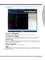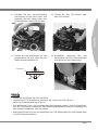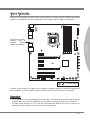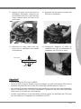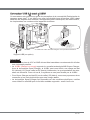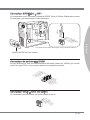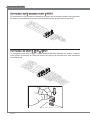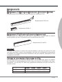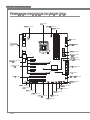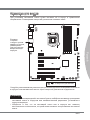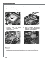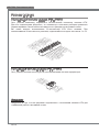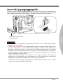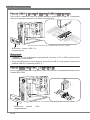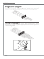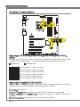
1
P67A-GD65/
P67A-GD55/
P67A-GD53/
P67S-GD53/
P67A-SD60 series
MS-7681 Mainboard
G52-76811X5
Preface
Copyright Notice
The material in this document is the intellectual property of MICRO-STAR INTERNATIONAL. We take every care in the preparation of this document, but no guarantee is
given as to the correctness of its contents. Our products are under continual improvement and we reserve the right to make changes without notice.
Trademarks
All trademarks are the properties of their respective owners.
■
■
■
■
■
■
■
■
■
■
■
■
MSI® is registered trademark of Micro-Star Int’l Co.,Ltd.
NVIDIA® is registered trademark of NVIDIA Corporation.
ATI® is registered trademark of ATI Technologies, Inc.
AMD® is registered trademarks of AMD Corporation.
Intel® is registered trademarks of Intel Corporation.
Windows® is registered trademarks of Microsoft Corporation.
AMI® is registered trademark of American Megatrends Inc.
Award® is a registered trademark of Phoenix Technologies Ltd.
Sound Blaster® is registered trademark of Creative Technology Ltd.
Realtek® is registered trademark of Realtek Semiconductor Corporation.
JMicron® is registered trademark of JMicron Technology Corporation.
Netware® is a registered trademark of Novell, Inc.
Revision History
Revision
Revision History
Date
V1.0
First release for Europe
October 2010
V1.1
Change cover
December 2010
Technical Support
If a problem arises with your system and no solution can be obtained from the user’s
manual, please contact your place of purchase or local distributor. Alternatively, please
try the following help resources for further guidance.
◙
◙
Visit the MSI website for FAQ, technical guide, BIOS updates, driver updates,
and other information: http://www.msi.com/index.php?func=service
Contact our technical staff at: http://ocss.msi.com
ii
MS-7681
Safety Instructions
Always read the safety instructions carefully.
Keep this User’s Manual for future reference.
Keep this equipment away from humidity.
Lay this equipment on a reliable flat surface before setting it up.
The openings on the enclosure are for air convection hence protects the equipment
from overheating. DO NOT COVER THE OPENINGS.
■ Make sure the voltage of the power source and adjust properly 110/220V before
connecting the equipment to the power inlet.
■ Place the power cord such a way that people can not step on it. Do not place anything over the power cord.
■ Always Unplug the Power Cord before inserting any add-on card or module.
■ All cautions and warnings on the equipment should be noted.
■ Never pour any liquid into the opening that could damage or cause electrical
shock.
■ If any of the following situations arises, get the equipment checked by service
personnel:
◯
The power cord or plug is damaged.
◯
Liquid has penetrated into the equipment.
◯
The equipment has been exposed to moisture.
◯
The equipment does not work well or you can not get it work according to User’s
Manual.
◯
The equipment has dropped and damaged.
◯
The equipment has obvious sign of breakage.
DO NOT LEAVE THIS EQUIPMENT IN AN ENVIRONMENT ABOVE 60oC (140oF),
IT MAY DAMAGE THE EQUIPMENT.
CAUTION: There is a risk of explosion, if battery is incorrectly replaced.
Replace only with the same or equivalent type recommended by the manufacturer.
警告使用者:
這是甲類資訊產品,在居住的環境中使用時,可能會造成無線電干擾,在這種情況下,
使用者會被要求採取某些適當的對策。
廢電池請回收
For better environmental protection, waste batteries should be
collected separately for recycleing special disposal.
iii
Preface
■
■
■
■
■
Preface
FCC-B Radio Frequency Interference Statement
This equipment has been tested and found
to comply with the limits for a Class B digital device, pursuant to Part 15 of the FCC
Rules. These limits are designed to provide
reasonable protection against harmful interference in a residential installation. This equipment generates, uses and can radiate
radio frequency energy and, if not installed and used in accordance with the instructions, may cause harmful interference to radio communications. However, there is no
guarantee that interference will not occur in a particular installation. If this equipment
does cause harmful interference to radio or television reception, which can be determined by turning the equipment off and on, the user is encouraged to try to correct the
interference by one or more of the measures listed below.
◯
Reorient or relocate the receiving antenna.
◯
Increase the separation between the equipment and receiver.
◯
Connect the equipment into an outlet on a circuit different from that to which the
receiver is connected.
◯
Consult the dealer or an experienced radio/television technician for help.
Notice 1
The changes or modifications not expressly approved by the party responsible for compliance could void the user’s authority to operate the equipment.
Notice 2
Shielded interface cables and A.C. power cord, if any, must be used in order to comply
with the emission limits.
VOIR LA NOTICE D’INSTALLATION AVANT DE RACCORDER AU RESEAU.
Micro-Star International
MS-7681
This device complies with Part 15 of the FCC Rules. Operation is subject to the following two conditions:
1) this device may not cause harmful interference, and
2) this device must accept any interference received, including interference that may
cause undesired operation.
iv
MS-7681
WEEE (Waste Electrical and Electronic Equipment) Statement
ENGLISH
To protect the global environment and as an environmentalist, MSI must remind you that...
DEUTSCH
Hinweis von MSI zur Erhaltung und Schutz unserer Umwelt
Gemäß der Richtlinie 2002/96/EG über Elektro- und Elektronik-Altgeräte dürfen Elektro- und Elektronik-Altgeräte nicht mehr als kommunale Abfälle entsorgt werden. MSI
hat europaweit verschiedene Sammel- und Recyclingunternehmen beauftragt, die in
die Europäische Union in Verkehr gebrachten Produkte, am Ende seines Lebenszyklus
zurückzunehmen. Bitte entsorgen Sie dieses Produkt zum gegebenen Zeitpunkt ausschliesslich an einer lokalen Altgerätesammelstelle in Ihrer Nähe.
FRANÇAIS
En tant qu’écologiste et afin de protéger l’environnement, MSI tient à rappeler ceci...
Au sujet de la directive européenne (EU) relative aux déchets des équipement électriques et électroniques, directive 2002/96/EC, prenant effet le 13 août 2005, que les
produits électriques et électroniques ne peuvent être déposés dans les décharges ou
tout simplement mis à la poubelle. Les fabricants de ces équipements seront obligés de
récupérer certains produits en fin de vie. MSI prendra en compte cette exigence relative
au retour des produits en fin de vie au sein de la communauté européenne. Par conséquent vous pouvez retourner localement ces matériels dans les points de collecte.
РУССКИЙ
Компания MSI предпринимает активные действия по защите окружающей среды,
поэтому напоминаем вам, что....
В соответствии с директивой Европейского Союза (ЕС) по предотвращению
загрязнения окружающей среды использованным электрическим и электронным
оборудованием (директива WEEE 2002/96/EC), вступающей в силу 13
августа 2005 года, изделия, относящиеся к электрическому и электронному
оборудованию, не могут рассматриваться как бытовой мусор, поэтому
производители вышеперечисленного электронного оборудования обязаны
принимать его для переработки по окончании срока службы. MSI обязуется
соблюдать требования по приему продукции, проданной под маркой MSI на
территории EC, в переработку по окончании срока службы. Вы можете вернуть
эти изделия в специализированные пункты приема.
Preface
Under the European Union (“EU”) Directive on Waste Electrical and Electronic Equipment, Directive 2002/96/EC, which takes effect on August 13, 2005,
products of “electrical and electronic equipment” cannot be discarded as municipal wastes anymore, and manufacturers of covered electronic equipment
will be obligated to take back such products at the end of their useful life. MSI will comply with the product take back requirements at the end of life of MSI-branded products
that are sold into the EU. You can return these products to local collection points.
Preface
ESPAÑOL
MSI como empresa comprometida con la protección del medio ambiente, recomienda:
Bajo la directiva 2002/96/EC de la Unión Europea en materia de desechos y/o equipos electrónicos, con fecha de rigor desde el 13 de agosto de 2005, los productos
clasificados como “eléctricos y equipos electrónicos” no pueden ser depositados en
los contenedores habituales de su municipio, los fabricantes de equipos electrónicos,
están obligados a hacerse cargo de dichos productos al termino de su período de vida.
MSI estará comprometido con los términos de recogida de sus productos vendidos en
la Unión Europea al final de su periodo de vida. Usted debe depositar estos productos
en el punto limpio establecido por el ayuntamiento de su localidad o entregar a una
empresa autorizada para la recogida de estos residuos.
NEDERLANDS
Om het milieu te beschermen, wil MSI u eraan herinneren dat….
De richtlijn van de Europese Unie (EU) met betrekking tot Vervuiling van Electrische
en Electronische producten (2002/96/EC), die op 13 Augustus 2005 in zal gaan kunnen niet meer beschouwd worden als vervuiling. Fabrikanten van dit soort producten
worden verplicht om producten retour te nemen aan het eind van hun levenscyclus.
MSI zal overeenkomstig de richtlijn handelen voor de producten die de merknaam MSI
dragen en verkocht zijn in de EU. Deze goederen kunnen geretourneerd worden op
lokale inzamelingspunten.
SRPSKI
Da bi zaštitili prirodnu sredinu, i kao preduzeće koje vodi računa o okolini i prirodnoj
sredini, MSI mora da vas podesti da…
Po Direktivi Evropske unije (“EU”) o odbačenoj ekektronskoj i električnoj opremi, Direktiva 2002/96/EC, koja stupa na snagu od 13. Avgusta 2005, proizvodi koji spadaju
pod “elektronsku i električnu opremu” ne mogu više biti odbačeni kao običan otpad i
proizvođači ove opreme biće prinuđeni da uzmu natrag ove proizvode na kraju njihovog
uobičajenog veka trajanja. MSI će poštovati zahtev o preuzimanju ovakvih proizvoda
kojima je istekao vek trajanja, koji imaju MSI oznaku i koji su prodati u EU. Ove proizvode možete vratiti na lokalnim mestima za prikupljanje.
POLSKI
Aby chronić nasze środowisko naturalne oraz jako firma dbająca o ekologię, MSI przypomina, że...
Zgodnie z Dyrektywą Unii Europejskiej (“UE”) dotyczącą odpadów produktów elektrycznych i elektronicznych (Dyrektywa 2002/96/EC), która wchodzi w życie 13 sierpnia
2005, tzw. “produkty oraz wyposażenie elektryczne i elektroniczne “ nie mogą być traktowane jako śmieci komunalne, tak więc producenci tych produktów będą zobowiązani
do odbierania ich w momencie gdy produkt jest wycofywany z użycia. MSI wypełni
wymagania UE, przyjmując produkty (sprzedawane na terenie Unii Europejskiej) wycofywane z użycia. Produkty MSI będzie można zwracać w wyznaczonych punktach
zbiorczych.
vi
MS-7681
TÜRKÇE
Çevreci özelliğiyle bilinen MSI dünyada çevreyi korumak için hatırlatır:
ČESKY
Záleží nám na ochraně životního prostředí - společnost MSI upozorňuje...
Podle směrnice Evropské unie (“EU”) o likvidaci elektrických a elektronických výrobků
2002/96/EC platné od 13. srpna 2005 je zakázáno likvidovat “elektrické a elektronické
výrobky” v běžném komunálním odpadu a výrobci elektronických výrobků, na které se
tato směrnice vztahuje, budou povinni odebírat takové výrobky zpět po skončení jejich životnosti. Společnost MSI splní požadavky na odebírání výrobků značky MSI,
prodávaných v zemích EU, po skončení jejich životnosti. Tyto výrobky můžete odevzdat
v místních sběrnách.
MAGYAR
Annak érdekében, hogy környezetünket megvédjük, illetve környezetvédőként fellépve
az MSI emlékezteti Önt, hogy ...
Az Európai Unió („EU”) 2005. augusztus 13-án hatályba lépő, az elektromos és elektronikus berendezések hulladékairól szóló 2002/96/EK irányelve szerint az elektromos
és elektronikus berendezések többé nem kezelhetőek lakossági hulladékként, és az
ilyen elektronikus berendezések gyártói kötelessé válnak az ilyen termékek visszavételére azok hasznos élettartama végén. Az MSI betartja a termékvisszavétellel kapcsolatos követelményeket az MSI márkanév alatt az EU-n belül értékesített termékek
esetében, azok élettartamának végén. Az ilyen termékeket a legközelebbi gyűjtőhelyre
viheti.
ITALIANO
Per proteggere l’ambiente, MSI, da sempre amica della natura, ti ricorda che….
In base alla Direttiva dell’Unione Europea (EU) sullo Smaltimento dei Materiali Elettrici
ed Elettronici, Direttiva 2002/96/EC in vigore dal 13 Agosto 2005, prodotti appartenenti
alla categoria dei Materiali Elettrici ed Elettronici non possono più essere eliminati come
rifiuti municipali: i produttori di detti materiali saranno obbligati a ritirare ogni prodotto
alla fine del suo ciclo di vita. MSI si adeguerà a tale Direttiva ritirando tutti i prodotti
marchiati MSI che sono stati venduti all’interno dell’Unione Europea alla fine del loro
ciclo di vita. È possibile portare i prodotti nel più vicino punto di raccolta
vii
Preface
Avrupa Birliği (AB) Kararnamesi Elektrik ve Elektronik Malzeme Atığı, 2002/96/EC
Kararnamesi altında 13 Ağustos 2005 tarihinden itibaren geçerli olmak üzere, elektrikli
ve elektronik malzemeler diğer atıklar gibi çöpe atılamayacak ve bu elektonik cihazların
üreticileri, cihazların kullanım süreleri bittikten sonra ürünleri geri toplamakla yükümlü
olacaktır. Avrupa Birliği’ne satılan MSI markalı ürünlerin kullanım süreleri bittiğinde MSI
ürünlerin geri alınması isteği ile işbirliği içerisinde olacaktır. Ürünlerinizi yerel toplama
noktalarına bırakabilirsiniz.
Preface
▍ Contents
Copyright Notice�������������������������������������������������������������������������������������������� ii
Trademarks���������������������������������������������������������������������������������������������������� ii
Revision History�������������������������������������������������������������������������������������������� ii
Technical Support����������������������������������������������������������������������������������������� ii
Safety Instructions�����������������������������������������������������������������������������������������iii
FCC-B Radio Frequency Interference Statement����������������������������������������� iv
WEEE (Waste Electrical and Electronic Equipment) Statement�������������������� v
English������������������������������������������������������������������������������������������������������ En-1
Mainboard Specifications�����������������������������������������������������������������������������������En-2
Quick Components Guide����������������������������������������������������������������������������������En-4
Screw Holes�������������������������������������������������������������������������������������������������������En-5
CPU (Central Processing Unit)��������������������������������������������������������������������������En-6
Memory������������������������������������������������������������������������������������������������������������En-10
Power Supply���������������������������������������������������������������������������������������������������En-12
Back Panel�������������������������������������������������������������������������������������������������������En-13
Connectors�������������������������������������������������������������������������������������������������������En-15
Jumpers�����������������������������������������������������������������������������������������������������������En-22
Buttons�������������������������������������������������������������������������������������������������������������En-23
Slots�����������������������������������������������������������������������������������������������������������������En-25
LED Status Indicators��������������������������������������������������������������������������������������En-26
BIOS Setup������������������������������������������������������������������������������������������������������En-27
Software Information����������������������������������������������������������������������������������������En-36
Deutsch���������������������������������������������������������������������������������������������������� De-1
Spezifikationen�������������������������������������������������������������������������������������������������� De-2
Komponenten-Übersicht����������������������������������������������������������������������������������� De-4
Schraubenlöcher����������������������������������������������������������������������������������������������� De-5
CPU (Prozessor)����������������������������������������������������������������������������������������������� De-6
Speicher���������������������������������������������������������������������������������������������������������� De-10
Stromversorgung��������������������������������������������������������������������������������������������� De-12
Rücktafel��������������������������������������������������������������������������������������������������������� De-13
Anschlüssen���������������������������������������������������������������������������������������������������� De-15
Steckbrücke���������������������������������������������������������������������������������������������������� De-22
Tasten������������������������������������������������������������������������������������������������������������� De-23
Steckplätze������������������������������������������������������������������������������������������������������ De-25
LED Statusanzeige����������������������������������������������������������������������������������������� De-26
BIOS Setup����������������������������������������������������������������������������������������������������� De-27
Software-Information��������������������������������������������������������������������������������������� De-36
viii
MS-7681
Français����������������������������������������������������������������������������������������������������� Fr-1
Spécifications������������������������������������������������������������������������������������������������������Fr-2
Guide Rapide Des Composants��������������������������������������������������������������������������Fr-4
Trous Taraudés���������������������������������������������������������������������������������������������������Fr-5
Connecteurs d’alimentation�������������������������������������������������������������������������������Fr-12
Panneau arrière������������������������������������������������������������������������������������������������Fr-13
Connecteurs������������������������������������������������������������������������������������������������������Fr-15
Cavalier�������������������������������������������������������������������������������������������������������������Fr-22
Bouton���������������������������������������������������������������������������������������������������������������Fr-23
Emplacements��������������������������������������������������������������������������������������������������Fr-25
Indicateur de statut LED������������������������������������������������������������������������������������Fr-26
Réglage BIOS���������������������������������������������������������������������������������������������������Fr-27
Information Logiciel�������������������������������������������������������������������������������������������Fr-36
Русский���������������������������������������������������������������������������������������������������� Ru-1
Характеристики����������������������������������������������������������������������������������������������� Ru-2
Размещение компонентов системной платы������������������������������������������������ Ru-4
Отверстия для винтов������������������������������������������������������������������������������������� Ru-5
CPU (Центральный процессор)���������������������������������������������������������������������� Ru-6
Память������������������������������������������������������������������������������������������������������������ Ru-10
Разъем питания��������������������������������������������������������������������������������������������� Ru-12
Задняя панель����������������������������������������������������������������������������������������������� Ru-13
Коннекторы���������������������������������������������������������������������������������������������������� Ru-15
Перемычки����������������������������������������������������������������������������������������������������� Ru-22
Кнопки������������������������������������������������������������������������������������������������������������ Ru-23
Слоты������������������������������������������������������������������������������������������������������������� Ru-25
Световые индикаторы����������������������������������������������������������������������������������� Ru-26
Настройка BIOS��������������������������������������������������������������������������������������������� Ru-27
Сведения о программном обеспечении������������������������������������������������������ Ru-36
ix
Preface
Processeur : CPU�����������������������������������������������������������������������������������������������Fr-6
Mémoire������������������������������������������������������������������������������������������������������������Fr-10
English
P67A-GD65/
P67A-GD55/
P67A-GD53/
P67S-GD53/
P67A-SD60
Series
Europe version
MS-7681 Mainboard
Mainboard Specifications
Processor Support
■ Intel® Sandy Bridge processor in the LGA1155 package
(For the latest information about CPU, please visit http://www.msi.com/index.
php?func=cpuform2)
Base Clock
■ 100 MHz
Chipset
■ Intel® P67 chipset
Memory Support
■ 4 DDR3 DIMMs support DDR3 2133*(OC)/ 1600*(OC)/ 1333/ 1066 DRAM (16GB
Max)
■ Supports Dual-Channel mode
*(For more information on compatible components, please visit
http://www.msi.com/index.php?func=testreport)
LAN
■ Supports LAN 10/100/1000 by Realtek® RTL8111E
IEEE 1394 (P67A-GD65/ P67A-GD55)
■ 2 IEEE 1394 ports by VIA® VT6308P (pinheader x1, rear panel x1)
Audio
■ Chip integrated by Realtek® ALC892
■ Flexible 8-channel audio with jack sensing
■ Compliant with Azalia 1.0 Spec
SATA
■ 4 SATA 3Gb/s ports (SATA3~6 by Intel® P67 PCH)
■ 4 SATA 6Gb/s ports (SATA1~2 by Intel® P67 PCH, SATA7~8 by Marvell® 9128)
(P67A-GD65)
■ 2 SATA 6Gb/s ports (SATA1~2 by Intel® P67 PCH) (P67A-GD55/ P67A-GD53/ P67SGD53/ P67A-SD60)
■ 2 eSATA ports (back panel) by JMicron® JMB362 (P67A-GD65)
RAID
■ SATA1~6 support Intel® Matrix Storage Technology (AHCI/ RAID 0/ 1/ 5/ 10) by Intel®
P67 PCH
■ SATA7~8 support RAID 0/ 1 mode by Marvell® SE9128 (P67A-GD65)
■ eSATA ports support RAID 0/ 1 & JBOD mode by JMicron® JMB362 (P67A-GD65)
USB 3.0 (P67A-GD65/ P67A-GD55/ P67A-GD53/ P67A-SD60)
■ 2 USB 3.0 ports by NEC® uPD720200F1
En-2
Connectors
Slots
■ 1 PCIE 2.0 x16 slot (PCI_E2)
■ 1 PCIE 2.0 x8 slot (in x16 slot)(PCI_E5)
■ 3 PCIE 2.0 x1 slots
■ 2 PCI slots, support 3.3V/ 5V PCI bus Interface
Form Factor
■ ATX (30.5cm X 24.5 cm)
Mounting
■ 9 mounting holes
If you need to purchase accessories and request the part numbers, you could search
the product web page and find details on our web address below
http://www.msi.com/index.php
En-3
English
■ Back panel
- 1 PS/2 keyboard/mouse port
- 1 Clear CMOS button (P67A-GD65/ P67A-GD55/ P67A-GD53/ P67S-GD53)
- 1 Coaxial S/PDIF-Out (P67A-GD65/ P67A-GD55/ P67A-GD53/ P67S-GD53)
- 1 Optical S/PDIF-Out (P67A-GD65/ P67A-GD55/ P67A-GD53/ P67S-GD53)
- 1 IEEE 1394 port (P67A-GD65/ P67A-GD55)
- 10 USB 2.0 ports (P67S-GD53)
- 8 USB 2.0 ports, 2 USB 3.0 ports (P67A-GD65/ P67A-GD55/ P67A-GD53/ P67ASD60)
- 2 eSATA ports (P67A-GD65)
- 1 LAN port
- 6 flexible audio ports
■ On-Board
- 2 USB 2.0 connectors (P67A-GD53/ P67S-GD53)
- 1 USB 2.0 connector, 1 USB 3.0 connector (P67A-GD65/ P67A-GD55/ P67ASD60)
- 1 IEEE 1394 connector (P67A-GD65/ P67A-GD55)
- 1 Chassis Intrusion connector
- 1 CD-In connector (P67A-GD65/ P67A-GD55/ P67A-GD53/ P67S-GD53)
- 1 S/PDIF-Out connector
- 1 Front Panel Audio connector
- 1 TPM Module connector
- 1 Serial connector
- 1 Reset button (P67A-GD65/ P67A-GD55/ P67S-GD53/ P67A-GD53)
- 1 Power button (P67A-GD65/ P67A-GD55/ P67S-GD53/ P67A-GD53)
- 1 OC Genie button (P67A-GD65/ P67A-GD55/ P67S-GD53/ P67A-GD53)
- 1 Voltage Check Point set (P67A-GD65)
MS-7681 Mainboard
Quick Components Guide
CPU, En-6
JPWR2, En-12
CPUFAN, En-16
DDR3, En-10
FV1, En-24
Back Panel,
En-13
SYSFAN3~4,
En-16
JPWR1, En-12
JDLED3, En-21
JBAT1, En-22
SYSFAN2, En-16
SYSFAN1, En-16
PCIE, En-25
SATA1~8, En-15
JCI1, En-15
JFP1, JFP2, En-16
PCI, En-25
TURBO1, En-23
JAUD1, En-20
RESET1, En-23
JCD1, En-19
POWER1, En-23
JSP1, En-19
JCOM1, En-19
JUSB2, En-18
J1394_1, En-18
JTPM1, En-20
JUSB1, En-17
En-4
Screw Holes
When you install the mainboard, you have to place the mainboard into the chassis in the
correct direction. The locations of screws holes on the mainboard are shown as below.
English
The side has to
toward the rear,
the position for
the I/O shield of
the chassis.
Screw holes
Refer above picture to install standoffs in the appropriate locations on chassis and then
screw through the mainboard screw holes into the standoffs.
Important
• To prevent damage to the mainboard, any contact between the mainboard circuit and
chassis or unnecessary standoffs mounted on the chassis is prohibited.
• Please make sure there are no metal components placed on the mainboard or within
the chassis that may cause short circuit of the mainboard.
En-5
MS-7681 Mainboard
CPU (Central Processing Unit)
When you are installing the CPU, make sure to install the cooler to prevent overheating.
If you do not have the CPU cooler, consult your dealer before turning on the computer.
For the latest information about CPU, please visit http://www.msi.com/index.
php?func=cpuform2
Important
Overheating
Overheating will seriously damage the CPU and system. Always make sure the cooling
fan can work properly to protect the CPU from overheating. Make sure that you apply
an even layer of thermal paste (or thermal tape) between the CPU and the heatsink to
enhance heat dissipation.
Replacing the CPU
While replacing the CPU, always turn off the ATX power supply or unplug the power
supply’s power cord from the grounded outlet first to ensure the safety of CPU.
Overclocking
This mainboard is designed to support overclocking. However, please make sure your
components are able to tolerate such abnormal setting, while doing overclocking. Any
attempt to operate beyond product specifications is not recommended. We do not guarantee the damages or risks caused by inadequate operation or beyond product specifications.
Introduction to LGA 1155 CPU
The surface of LGA 1155 CPU. Remember to apply some thermal paste on it for
better heat dispersion.
Alignment Key
Yellow triangle is the
Pin 1 indicator
En-6
Alignment Key
CPU & Cooler Installation
When you are installing the CPU, make sure the CPU has a cooler attached on the top
to prevent overheating. Meanwhile, do not forget to apply some thermal paste on CPU
before installing the heat sink/cooler fan for better heat dispersion.
Follow the steps below to install the CPU & cooler correctly. Wrong installation will
cause the damage of your CPU & mainboard.
2. Lift the load lever up to fully open
position
3. The CPU socket has a plastic cap on
it to protect the contact from damage.
Before you install CPU, always cover
it to protect the socket pin. Romove
the cap (as the arrow shows).
4. After confirming the CPU direction for
correct mating, put down the CPU in
the socket housing frame. Be sure to
grasp on the edge of the CPU base.
Note that the alignment keys are
matched.
Alignment Key
En-7
English
1. Open the load level. MS-7681 Mainboard
5. Visually inspect if the CPU is seated
well into the socket. If not, take out
the CPU with pure vertical motion
and reinstall.
6. Engage the load lever while pressing
down lightly onto the load plate.
Alignment Key
7. Secure the lever near the hook end
under the retention tab.
8. Make sure the four hooks are in porper position before you install the
cooler.
Important
• Confirm if your CPU cooler is firmly installed before turning on your system.
• Do not touch the CPU socket pins to avoid damaging.
En-8
10. Press the four hooks down to fasten
the cooler.
11. Turn over the mainboard to confirm
that the clip-ends are correctly inserted.
12. Finally, attach the CPU Fan cable to
the CPU fan connector on the mainboard.
English
9. Align the holes on the mainboard with
the heatsink. Push down the cooler
until its four clips get wedged into the
holes of the mainboard.
Mainboard
Hook
Important
• Read the CPU status in BIOS.
• Whenever CPU is not installed, always protect your CPU socket pin with the plastic
cap covered (shown in Figure 1) to avoid damaging.
• Mainboard photos shown in this section are for demonstration of the CPU/ cooler installation only. The appearance of your mainboard may vary depending on the model
you purchase.
• Please refer to the documentation in the CPU fan package for more details about the
CPU fan installation.
En-9
MS-7681 Mainboard
Memory
These DIMM slots are used for installing memory modules. For more information on
compatible components, please visit http://www.msi.com/index.php?func=testreport
DDR3
240-pin, 1.5V
48x2=96 pin
72x2=144 pin
Memory Population Rule
Please refer to the following illustrations for memory population rules.
Dual-Channel mode Population Rule
In Dual-Channel mode, the memory modules can transmit and receive data with two
data bus lines simultaneously. Enabling Dual-Channel mode can enhance the system
performance. The following illustrations explain the population rules for Dual-Channel
mode.
1
DIMM1
DIMM2
DIMM3
DIMM4
2
DIMM1
DIMM2
DIMM3
DIMM4
Installed
Empty
Important
• DDR3 memory modules are not interchangeable with DDR2, and the DDR3 standard
is not backwards compatible. You should always install DDR3 memory modules in
the DDR3 DIMM slots.
• In Dual-Channel mode, make sure that you install memory modules of the same type
and density in different channel DIMM slots.
• To ensure a successful system boot-up, always insert the memory modules into the
DIMM1 first.
• Due to the chipset resource deployment, the system density will only be detected up
to 15+GB (not full 16GB) when each DIMM is installed with a 4GB memory module.
En-10
Installing Memory Modules
1. The memory module has only one notch on the center and will only fit in the right
orientation.
3. Manually check if the memory module has been locked in place by the DIMM slot
clips at the sides.
Notch
Volt
Important
You can barely see the golden finger if the memory module is properly inserted in the
DIMM slot.
En-11
English
2. Insert the memory module vertically into the DIMM slot. Then push it in until the
golden finger on the memory module is deeply inserted in the DIMM slot. The plastic
clip at each side of the DIMM slot will automatically close when the memory module
is properly seated.
MS-7681 Mainboard
Power Supply
ATX 24-pin Power Connector: JPWR1
This connector allows you to connect an ATX 24-pin power supply. To connect the ATX
24-pin power supply, make sure the plug of the power supply is inserted in the proper
orientation and the pins are aligned. Then push down the power supply firmly into the
connector.
You may use the 20-pin ATX power supply as you like. If you’d like to use the 20-pin
ATX power supply, please plug your power supply along with pin 1 & pin 13.
d
n
u
ro
V
.G 5 V
4
2 3.+ +5 V
d
2 2. 5 s n d
2 1.+ Re ou un d
2 0. Gr ro un #
2 9. G o N d
1 8. Gr -O un
1 7. PS o
1 6. Gr 2V V
1 5. 1 .3
1 4.- +3
1 3.
1
V
.3
3 V
.+ 2 V
2 1 2
1 .+ +1 B OK
11 0. S R d
1 .5V W un
d
9 .P ro
8 .G 5V un
7 .+ ro nd
6 .G 5V u
5 + o V
r
.
4 .G 3.3 3V
.
3
+
.
3
2 .+
1
ATX 8-pin Power Connector: JPWR2
This connector is used to provide the power output to the CPU.
d
n
u d
ro un nd
.G ro u d
4 .G ro un
3 .G ro
2 .G
1
V
2
1 V
.+ 2 V
8 .+1 2 V
7 .+1 12
6 .+
5
Important
Make sure that all the connectors are connected to proper ATX power supplies to ensure stable operation of the mainboard.
En-12
Back Panel
IEEE 1394 Port
(optional)
Mouse/
Keyboard
Coaxial
S/PDIF-Out
(optional)
LAN
USB 2.0 Port
RS-Out
Line-Out CS-Out
USB 2.0 Port
Optical
S/PDIF-Out
(optional)
Clear CMOS Button
(optional)
USB 2.0 Port
eSATA Port
(optional)
Mic SS-Out
USB 3.0 Port
(optional)
▶ Mouse/Keyboard
The standard PS/2® mouse/keyboard DIN connector is for a PS/2® mouse/keyboard.
▶ Clear CMOS Button (optional)
There is a CMOS RAM on board that has a power supply from external battery to keep
the system configuration data. With the CMOS RAM, the system can automatically
boot OS every time it is turned on. If you want to clear the system configuration, use
the button to clear data. Press the button to clear the data.
Important
• Make sure that you power off the system before clearing CMOS data.
• After pressing this button to clear CMOS data in power off (G3) state, the system will
boot automatically.
▶ Coaxial S/PDIF-Out (optional)
This SPDIF (Sony & Philips Digital Interconnect Format) connector is provided for digital
audio transmission to external speakers through a coaxial cable.
▶ Optical S/PDIF-Out (optional)
This SPDIF (Sony & Philips Digital Interconnect Format) connector is provided for digital
audio transmission to external speakers through an optical fiber cable.
▶ IEEE 1394 Port (optional)
The IEEE 1394 port on the back panel provides connection to IEEE 1394 devices.
▶ eSATA Port (optional)
The eSATA (External SATA) port is for attaching the eSATA hard drive.
En-13
English
Line-In
MS-7681 Mainboard
▶ USB 2.0 Port
The USB (Universal Serial Bus) port is for attaching USB devices such as keyboard,
mouse, or other USB-compatible devices. Supports data transfer rate up to 480Mbit/s
(Hi-Speed).
▶ USB 3.0 Port (optional)
USB 3.0 port is backward-compatible with USB 2.0 devices. It supports data transfer
rate up to 5 Gbit/s (SuperSpeed).
Important
If you want to use a USB 3.0 device, you must use the USB 3.0 cable to connect to the
USB 3.0 port.
▶ LAN
The standard RJ-45 LAN jack is for connection to
the Local Area Network (LAN). You can connect a
network cable to it.
Yellow
LED
Color
LED State
Condition
Left
Yellow
Off
LAN link is not established.
On(Steady state)
LAN link is established.
Right
Green/ Orange
On(brighter & pulsing)
The computer is communicating with another computer on the LAN.
Green
Off
10 Mbit/sec data rate is selected.
On
100 Mbit/sec data rate is selected.
Orange
On
1000 Mbit/sec data rate is selected.
▶ Audio Ports
These audio connectors are used for audio devices. It is easy to differentiate between
audio effects according to the color of audio jacks.
■ Line-In: Blue - Line In, is used for external CD player, tape-player or other audio
devices.
■ Line-Out: Green - Line Out, is a connector for speakers or headphones.
■ Mic: Pink - Mic, is a connector for microphones.
■ RS-Out: Black (optional) - Rear-Surround Out in 4/ 5.1/ 7.1 channel mode.
■ CS-Out: Orange (optional)- Center/ Subwoofer Out in 5.1/ 7.1 channel mode.
■ SS-Out: Gray (optional)- Side-Surround Out 7.1 channel mode.
En-14
Connectors
Serial ATA Connector: SATA1~8 (optional)
This connector is a high-speed Serial ATA interface port. Each connector can connect
to one Serial ATA device.
English
* The MB layout in this figure is for reference only.
SATA1_2
SATA3_4
SATA5_6
SATA1~2 & SATA7~8 (6Gb/s)
SATA3~6 (3Gb/s)
SATA7_8
Important
Please do not fold the Serial ATA cable into a 90-degree angle. Otherwise, data loss
may occur during transmission.
Chassis Intrusion Connector: JCI1
This connector connects to the chassis intrusion switch cable. If the chassis is opened,
the chassis intrusion mechanism will be activated. The system will record this status
and show a warning message on the screen. To clear the warning, you must enter the
BIOS utility and clear the record.
d
n
u RU
ro T
.G IN
2 .C
1
En-15
MS-7681 Mainboard
Fan Power Connectors: CPUFAN,SYSFAN1~4
The fan power connectors support system cooling fan with +12V. When connecting the
wire to the connectors, always note that the red wire is the positive and should be connected to the +12V; the black wire is Ground and should be connected to GND. If the
mainboard has a System Hardware Monitor chipset on-board, you must use a specially
designed fan with speed sensor to take advantage of the CPU fan control.
CPUFAN
SYSFAN1~4
d
n
u
ro 2V or
.G 1 s
1 .+ en
2 .S
3
d
n
u
ro 2V or l
.G 1 s o
1 .+ en tr
2 .S on
3 .C
4
Important
• Please refer to the recommended CPU fans at processor’s official website or consult
the vendors for proper CPU cooling fan.
• CPUFAN support Smart fan control. You can install Control Center utility that will
automatically control the CPUFAN speeds according to the actual CPUFAN temperatures.
• Fan cooler set with 3 or 4 pins power connector are both available for CPUFAN.
Front Panel Connectors: JFP1, JFP2
These connectors are for electrical connection to the front panel switches and LEDs.
The JFP1 is compliant with Intel® Front Panel I/O Connectivity Design Guide.
P
o
w
e
r
r
L
E
D
r
Buz
zer
JFP2
D D
in E LE
P rL d
o e n
.N w e d
7 .Po sp n
5 Su rou
.
3 .G
1
ch
it
w
d
e tS
rv e
D
s
E
se e
L
e R
D
.R
D
9 .+
H
7 .5
.
3 .+
1
En-16
ake
.+
8 .
6
+
.
4 .
2
in
P o 8. +
.
.N
6
0
.
4 +
.
2
e
ch
w
it
o
w
1
S
P
JFP1
Spe
Front USB 2.0 Connector: JUSB1
This connector, compliant with Intel® I/O Connectivity Design Guide, is ideal for connecting high-speed USB interface peripherals such as USB HDD, digital cameras, MP3
players, printers, modems and the like.
115V
English
d
C un +
.N o 1
0 r B 11 .G
8 S B
.U S
6 .U C
4 VC
.
2
in
P nd
o u +
.N ro 0
9 .G SB 07 U B
.
S
5 .U CC
3 .V
1
* The MB layout in this figure is for reference only.
USB Bracket (optional)
Important
• Note that the pins of VCC and GND must be connected correctly to avoid possible
damage.
• The JUSB1 (red mark) supports MSI newly Super-Charger technology. With SuperCharger technology, the JUSB1 can only provide charging function in S0 (power-on),
S3 (sleep mode) & S5 (shut-down) states. However, the synchronizing data link will
be disabled. In this case, the system can not be awaked through the JUSB1.
• For Super-Charger in S3 (sleep mode)/ S5 (shut-down), we suggest you to connect
only one device for stable charging.
• Super-Charger technology would be available on specific models, please refer to MSI
website for model support list.
En-17
MS-7681 Mainboard
Front USB 3.0 Connector: JUSB2 (optional)
USB 3.0 port is backward-compatible with USB 2.0 devices. Supports data transfer rate
up to 5 Gbit/s (SuperSpeed).
115V
1 N
C D P
C _
in V 4 _D DN
P _ X 4
_ P
o B _R X
C D
_ _
.N S 3 R
4 C
0 U B _
2 .F S B3 nd X 4_
T
9
1 8.U S ou _ X
1 7.U r B3 _T
1 6.G S B3 nd
1 .U S u o
5
1 4.U r D1 +
1 3.G B D1
1 2.S B
1 1.S
1
2 N
C D
C _ P
V 3 D DN
_ X 3_
_ P
B R X
C D
S _ R
_ _
U B3 _
3 C
.F S 3 d X _
1 .U SB un T 3
2 .U ro 3_ TX
3 .G SB 3_ d
4 .U B n
5 US rou 0.
6 .G BD 0+
D
7
.S
8 .SB C
9 0.N
1
* The MB layout in this figure is for reference only.
USB 3.0 Bracket (optional)
Important
• Note that the pins of VCC and GND must be connected correctly to avoid possible
damage.
• If you want to use a USB 3.0 device, you must use the USB 3.0 cable to connect to
the USB 3.0 port.
IEEE1394 Connector: J1394_1 (optional)
This connector allows you to connect the IEEE1394 device via an optional IEEE1394
bracket.
* The MB layout in this figure is for reference only.
1394 Bracket (optional)
En-18
S/PDIF-Out Connector: JSP1
This connector is used to connect S/PDIF (Sony & Philips Digital Interconnect Format)
interface for digital audio transmission.
115V
English
d
n
u F
ro DI
.G P
1 .S CC
2 .V
3
* The MB layout in this figure is for reference only.
S/PDIF-Out Bracket (optional)
Serial Port Connector: JCOM1
This connector is a 16550A high speed communication port that sends/receives 16
bytes FIFOs. You can attach a serial device.
in
P
o
.N S
0 T R
1 .C S
8
.D R
6 DT N
.
4 SI
.
2
I S d
.R T n
9 . R r ou T
7 .G U
5 . SO C D
3 .D
1
CD-In Connector: JCD1 (optional)
This connector is provided for external audio input.
d
n
u nd
.L ro u
1 .G ro
2 G
.
3 .R
4
En-19
MS-7681 Mainboard
Front Panel Audio Connector: JAUD1
This connector allows you to connect the front panel audio and is compliant with Intel®
Front Panel I/O Connectivity Design Guide.
ct
te
e
D
e
n
o
n
h
io
P
ct
d
e
a
e in et
.H P D
0 o
1 .N IC
d
8 M
n
.
C
u
6
N
o
.
4 Gr
.
2
io
n
L
e D
n
o N
h E R
P _S ne
d
o
a E h
e NS P
.H E d
9 .S ea R
7 .H IC L
5 .M IC
3 .M
1
TPM Module connector: JTPM1
This connector connects to a TPM (Trusted Platform Module) module (optional). Please
refer to the TPM security platform manual for more details and usages.
3
in
p 2
ta in
a p 1
d ta pin 0
n
e s & da ta pi
m s & da ta
a
ra re s
F d s & d
C ad dre ss &
P
re s
.L C d d s
3 P a d re
1 1.L C a dd et
1 .LP C a es k
9 .LP C R loc
7 .LP C C
5 .L P C
3 .LP
1
d
n
u nd
r
ro u n r
e
.G ro Pi we Q r ow
4
1 2 . G o P o IR w e y p
1 .N V ial o b
0
1 .5 er P nd
8 S 3V ta
.
6 3. S
.
4 .3V
2
En-20
DLED3 Connector: JDLED3 (optional)
This is reserved for connecting the msi future control card.
English
in
p
d
n d
u rve
ro se d in
p
.G e n l in
u
p
3
1 .R o tro l in
r
11 .G on tro l p
o
n
9
C
tr
.
7 .Co n B
o
5 C S
.
3 .5V
1
in
p n
l i
o p
tr l
n
n o
o ntr n pi
.C o Pi ol
n
4
1 2.C o tr d pi n
1 .N on un l pi
0
1 .C ro tro l
8 .G n ro
t
6 Co n
.
4 .Co
2
En-21
MS-7681 Mainboard
Jumpers
Clear CMOS Jumper: JBAT1
There is a CMOS RAM on board with an external battery power supply to preserve the
system configuration data. With the CMOS RAM, the system can automatically boot OS
every time it is turned on. If you want to clear the system configuration, set the jumper
to clear data.
1
JBAT1
1
Keep Data
1
Clear Data
Important
You can clear CMOS by shorting 2-3 pin while the system is off. Then return to 12 pin position. Avoid clearing the CMOS while the system is on; it will damage the
mainboard.
En-22
Buttons
This section will explain how to change your motherboard’s function through the use of
following buttons.
OC Genie Button: TURBO1 (optional)
Important
Please install the DDR3 1333 and up memory and equip better heat sink/ cooler with
OC Genie function.
We do not guarantee the OC Genie overclocking range and the damages or risks
caused by the OC Genie overclocking behavior.
You can disable the OC Genie function in BIOS setup. And we suggest you to save the
OC Genie configuration to overclocking profile in BIOS for future using.
Power Button: POWER1 (optional)
This power button is used to turn-on or turn-off the system. Press the button to turn-on
or turn-off the system.
Reset Button: RESET1 (optional)
This reset button is used to reset the system. Press the button to reset the system.
En-23
English
This button is used to auto-overclock for the system. Press this button to enable the
OC Genie function when the system is in power off state, meanwhile, the button will
light and lock. And then the system will automatically detect the optimum values to
overclock after booting the system. To disable the OC Genie function, please press the
button again after power off the system, meanwhile, the button light will off and unlock,
and the system will restore the default for next boot.
MS-7681 Mainboard
Voltage Check Point: FV1 (optional)
This voltage check point set is used to measure the current CPU/ CPU_VTT/ CPU_SA/
DDR/ PCH voltage.
CPU
CPU_SA
PCH
GND
7
1
CPU_VTT
1
CPU
CPU_VTT
CPU_SA
7
CPU_VTT voltage: measure the current CPU_
VTT voltage with CPU_VTT point and GND
point by using a multimeter.
7
CPU_SA voltage: measure the current CPU_SA
voltage with CPU_SA point and GND point by
using a multimeter.
7
DDR voltage: measure the current DDR voltage
with DDR point and GND point by using a multimeter.
7
PCH voltage: measure the current PCH voltage
with PCH point and GND point by using a multimeter.
GND
1
DDR
GND
1
PCH
En-24
CPU voltage: measure the current CPU voltage
with CPU point and GND point by using a multimeter.
GND
1
GND
GND
7
GND
1
DDR
Slots
PCIE (Peripheral Component Interconnect Express) Slot
The PCIE slot supports the PCIE interface expansion card.
English
PCIE x16 Slot
PCIE x1 Slot
PCI (Peripheral Component Interconnect) Slot
The PCI slot supports LAN card, SCSI card, USB card, and other add-on cards that
comply with PCI specifications.
32-bit PCI Slot
Important
When adding or removing expansion cards, make sure that you unplug the power supply first. Meanwhile, read the documentation for the expansion card to configure any
necessary hardware or software settings for the expansion card, such as jumpers,
switches or BIOS configuration.
PCI Interrupt Request Routing
The IRQ, acronym of interrupt request line and pronounced I-R-Q, are hardware lines
over which devices can send interrupt signals to the microprocessor. The PCI IRQ pins
are typically connected to the PCI bus pins as follows:
Order1
Order2
Order3
Order4
PCI Slot1
INT A#
INT B#
INT C#
INT D#
PCI Slot2
INT B#
INT C#
INT D#
INT A#
En-25
MS-7681 Mainboard
LED Status Indicators
APS LEDs
(optional)
Dual BIOS LED
(optional)
APS LED (P67A-GD65/ P67A-GD55/ P67A-GD53/ P67S-GD53)
The APS (Active Phase Switching) LED indicate the current CPU power phase mode.
Follow the instructions below to read.
: Lights
: Off
CPU is in 1 phase power mode.
CPU is in 2 phase power mode.
CPU is in 3 phase power mode.
CPU is in 4 phase power mode.
CPU is in 5 phase power mode.
CPU is in 6 phase power mode.
Dual BIOS LED (P67A-GD65)
The Dual BIOS LED indicates the BIOS status during system power on. Follow the
instructions below to read.
Off: Normal.
Blink (1 cycle/second): The primary BIOS is failed.
Fast Blink (10 cycles/second): The second BIOS is failed.
Solid: Both of primary and second BIOS are failed.
En-26
BIOS Setup
Important
• The items under each BIOS category described in this chapter are under continuous
update for better system performance. Therefore, the description may be slightly different from the latest BIOS and should be held for reference only.
• Upon boot-up, the 1st line appearing after the memory count is the BIOS version. It is
usually in the format:
E7681IMS.xxx 102410 where:
1st digit refers to BIOS type as E = EFI
2nd - 5th digit refers to the model number.
6th digit refers to the chipset as I = Intel, N = nVidia, A = AMD and V = VIA.
7th - 8th digit refers to the customer as MS = all standard customers.
xxx refers to the BIOS version.
102410 refers to the date this BIOS was released.
Entering Setup
Power on the computer and the system will start POST (Power On Self Test) process.
When the message below appears on the screen, press <DEL> key to enter Setup.
Press DEL to enter Setup Menu, F11 to enter Boot Menu
If the message disappears before you respond and you still wish to enter Setup, restart
the system by turning it OFF and On or pressing the RESET button. You may also restart the system by simultaneously pressing <Ctrl>, <Alt>, and <Delete> keys.
En-27
English
This chapter provides basic information on the BIOS Setup program and allows you to
configure the system for optimum use. You may need to run the Setup program when:
■ An error message appears on the screen during the system booting up, and
requests you to run BIOS SETUP.
■ You want to change the default settings for customized features.
MS-7681 Mainboard
Control
Keyboard
Mouse
<↑ ↓ >
Description
Select Item
Move the cursor
<Enter>
Select Icon/ Field
Click/ Doubleclick the left button
<Esc>
Jumps to the Exit menu or returns to the previous from
a submenu
Click the right
button
<+>
Increase the numeric value or make changes
<->
Decrease the numeric value or make changes
<F1>
General Help
<F4>
CPU Specifications
<F5>
Enter Memory-Z
<F6>
Load optimized defaults
<F10>
Save Change and Reset
<Esc>
Exit
Sub-Menu
If you find a right pointer symbol (as shown in the right view) appears to the left of certain fields that means a sub-menu can be launched from this field. A sub-menu contains
additional options for a field parameter. You can use arrow keys ( ↑↓ ) or mouse to
highlight the field and press <Enter> or double-click the left mouse button to enter the
sub-menu. Then you can use the control keys to enter values and move from field to
field within a sub-menu. If you want to return to the previous menu, just press the <Esc
> or click the right mouse button.
General Help <F1>
The BIOS setup program provides a General Help screen. You can call up this screen
from any menu by simply pressing <F1>. The Help screen lists the appropriate keys to
use and the possible selections for the highlighted item. Press <Esc> to exit the Help
screen.
En-28
The Main Menu
Once you enter BIOS CMOS Setup Utility, the Main Menu will appear on the screen.
The Main Menu allows you to select from the setup functions.
English
▶ Language
After entering the Setup menu, you can see a “Language” button. Please click it and
select the language, at your desire, for the BIOS setting first.
▶ Green Power
Click “Green Power” icon to enter the menu. Use this menu to specify the power
phase.
▶ Utility
Click “Utility” icon to enter the menu. This menu provides the useful utility for you to live
update bios and hard disk backup.
▶ OC
Click “OC” icon to enter the menu. Use this menu to specify your settings for frequency/
voltage control and overclocking.
▶ Game
Click “Game” icon to enter the menu. This menu provides several games for you to
play.
▶ Setting
Click “Setting” icon to enter the menu. Use this menu to specify your settings for chipset
features, boot device and password.
En-29
MS-7681 Mainboard
When enter the BIOS Setup utility, follow the processes below for general use.
1. Load Optimized Defaults : Select [Setting] -> [Save & Exit] -> [Restore Defaults] and
click on it. And then the screen shows a pop-up message as below. Select [Yes]
and click on it to load the default settings for optimal system performance.
2. Setup Date/ Time : Select [Setting] -> [System Status] -> [System Date]/ [System
Time] and click on it. And then, you can key-in the Date, Time in their respective
fields.
3. Save & Exit Setup : Select [Setting] -> [Save & Exit] -> [Save Changes & Reset]
and click on it. And then the screen shows a pop-up message as below. Select
[Yes] and click on it to save the configurations and exit BIOS setup utility.
En-30
4. OC Menu Introduction : This menu is for advanced user who want to overclock the
mainboard.
English
▶ Current CPU / DRAM Frequency
These items show the current clocks of CPU and Memory speed. Read-only.
▶ CPU Base Frequency [10KHz]
This item allows you to set the CPU Base clock (in 10KHz). You may overclock the CPU
by adjusting this value. Please note the overclocking behavior is not guaranteed.
▶ Adjust CPU Ratio
This item controls the multiplier that is used to determine the internal clock speed of the
processor relative to the external or motherboard clock speed. It is available only when
the processor supports this function.
▶ Adjusted CPU Frequency
It shows the adjusted CPU frequency. Read-only.
▶ EIST
The Enhanced Intel SpeedStep technology allows you to set the performance level of
the microprocessor. This field will appear after you installed the CPU which supports
speedstep technology.
En-31
MS-7681 Mainboard
▶ Intel Turbo Booster
This item will appear when you install a CPU with Intel Turbo Boost technology. This
item is used to enable/ disable Intel Turbo Boost technology. It can scale processor
frequency higher dynamically when applications demand more performance and TDP
headroom exists. It also can deliver seamless power scalability (Dynamically scale up,
Speed-Step Down). It is the Intel newly technology within newly CPU.
▶ DRAM Ratio
This setting controls the ratio of memory frequency to enable the memory to run at different frequency combinations.
▶ Extreme Memory Profile(X.M.P)
This item is used to enable/disable the Intel Extreme Memory Profile (XMP). For further
information please refer to Intel’s official website.
▶ Adjusted DRAM Frequency
It shows the adjusted DRAM frequency. Read-only.
▶ DRAM Timing Mode
Select whether DRAM timing is controlled by the SPD (Serial Presence Detect) EEPROM on the DRAM module. Setting to [Auto] enables DRAM timings and the following
“Advanced DRAM Configuration” sub-menu to be determined by BIOS based on the
configurations on the SPD. Selecting [Link] or [Unlink] allows users to configure the
DRAM timings and the following related “Advanced DRAM Configuration” sub-menu
manually.
▶ Advanced DRAM Configuration
Press <Enter> to enter the sub-menu.
▶ Command Rate2
This setting controls the DRAM command rate.
▶ tCL
This controls the CAS latency, which determines the timing delay (in clock cycles)
before SDRAM starts a read command after receiving it.
▶ tRCD
When DRAM is refreshed, both rows and columns are addressed separately. This
setup item allows you to determine the timing of the transition from RAS (row address strobe) to CAS (column address strobe). The less the clock cycles, the faster
the DRAM performance.
▶ tRP
This setting controls the number of cycles for Row Address Strobe (RAS) to be
allowed to precharge. If insufficient time is allowed for the RAS to accumulate its
charge before DRAM refresh, refreshing may be incomplete and DRAM may fail
to retain data. This item applies only when synchronous DRAM is installed in the
system.
▶ tRAS
This setting determines the time RAS takes to read from and write to memory cell.
En-32
▶ tRFC
This setting determines the time RFC takes to read from and write to a memory
cell.
▶ tWR
Minimum time interval between end of write data burst and the start of a precharge
command. Allows sense amplifiers to restore data to cells.
▶ tRRD
Specifies the active-to-active delay of different banks.
▶ tRTP
Time interval between a read and a precharge command.
▶ tFAW
This item is used to set the tFAW (four activate window delay) timing.
▶ tWCL
This item is used to set the tWCL (Write CAS Latency) timing.
▶ tCKE
This item is used to set the tCKE timing.
▶ Advanced Channel 1/ 2 Timing Configuration
Press <Enter> to enter the sub-menu. And you can set the advanced memory timing
for each channel.
▶ tRRDR/ tRRDD/ tWWDR/ tWWDD/ tRWDRDD/ tWRDRDD/ tRWSR
These items is used to set the memory timings for memory channel 1/ 2.
▶ VDroop Control
This item is used to select the VDroop control mode.
▶ CPU Vcore/ CPU IO/ DRAM Voltage/ CPU SA/ CPU PLL Voltage/ DDR_VREF_CA_A/
DDR_VREF_CA_B/ DDR_VREF_DA_A/ DDR_VREF_DA_B/ PCH 1.05
These items are used to adjust the voltage of CPU, Memory and chipset.
▶ Current CPU Vcore/ Current CPU IO/ Current DRAM Voltage/ Current CPU SA
These items show current CPU Vcore/ CPU IO/ DRAM voltage. Read-only.
▶ Overclocking Profile
Press <Enter> to enter the sub-menu.
▶ Overclocking Profile 1/ 2/ 3/ 4/ 5/ 6
Press <Enter> to enter the sub-menu. In the sub-menu, these items are used to save
the current settings, and you can to load the settings from the stored profile.
▶ OC Retry Count
When overclocking has failed, setting this item as [1, 3] will allow system to reboot
1/ 3 times with the same overclocked configuration. If overclocking has failed every
time, the system will restore the defaults.
En-33
English
▶ tWTR
Minimum time interval between the end of write data burst and the start of a column-read command. It allows I/O gating to overdrive sense amplifiers before read
command starts.
MS-7681 Mainboard
▶ CPU Specifications
Press <Enter> to enter the sub-menu. The submenu shows the information of installed
CPU.
▶ CPU Technology Support
Press <Enter> to enter the sub-menu. The sub-menu shows the installed CPU technologies. Read only.
▶ MEMORY-Z
Press <Enter> to enter the sub-menu.
▶ DIMM1~4 Memory SPD
Press <Enter> to enter the sub-menu. The sub-menu displays the informations of
installed memory.
▶ X.M.P Support Information
Press <Enter> to enter the sub-menu. These items display the current status of the
X.M.P support information. Read only.
▶ CPU Feature
Press <Enter> to enter the sub-menu and the following screen appears:
▶ Active Processor Cores
This item allows you to select the number of active processor cores.
▶ Limit CPUID Maximum
It is designed to limit the listed speed of the processor to older operating systems.
▶ Execute Disable Bit
Intel’s Execute Disable Bit functionality can prevent certain classes of malicious
“buffer overflow” attacks when combined with a supporting operating system. This
functionality allows the processor to classify areas in memory by where application
code can execute and where it cannot. When a malicious worm attempts to insert
code in the buffer, the processor disables code execution, preventing damage or
worm propagation.
▶ Intel Virtualization Tech
This item is used to enable/disable the Intel Virtualization technology. For further
information please refer to Intel’s official website.
▶ Power Technology
This item allows you to select the Intel Dynamic Power technology mode.
▶ C1E Support
To enable this item to read the CPU power consumption while idle. Not all processors
support Enhanced Halt state (C1E).
▶ OverSpeed Protection
Overspeed Protection function can monitor the current CPU draws as well as its
power consumption. If it exceeds a certain level, the processor automatically reduces
its clock speed. If you want to overclock your CPU, set it to [Disabled].
En-34
▶ Intel C-State
C-state is a power management state that significantly reduces the power of the
processor during idle. This field will appear after you installed the CPU which supports c-state technology.
▶ Package C-State limit
This feild allows you to select a C-state mode.
▶ Long duration maintained(ms)
This feild allows you to adjust the maintaining time for long duration power limit.
▶ Short duration power limit(W)
This feild allows you to adjust the TDP power limit for the short duration.
▶ 1/2/3/4-Core Ratio Limit
These feilds show the 1/2/3/4 core ratio limit of CPU.
En-35
English
▶ Long duration power limit(W)
This feild allows you to adjust the TDP power limit for the long duration.
MS-7681 Mainboard
Software Information
Take out the Driver/Utility DVD that is included in the mainboard package, and place
it into the DVD-ROM drive. The installation will auto-run, simply click the driver or utility and follow the pop-up screen to complete the installation. The Driver/Utility DVD
contains the:
- Driver menu : It provides available drivers. Install the driver by your desire and to
activate the device.
- Utility menu : It allows you to install the available software applications.
- Service base menu : Through this menu to link the MSI officially website.
- Product info menu : It shows the newly information of MSI product.
- Security menu : It provides the useful antivirus program.
Important
Please visit the MSI officially website to get the latest drivers and BIOS for better system
performance.
En-36
Deutsch
P67A-GD65/
P67A-GD55/
P67A-GD53/
P67S-GD53/
P67A-SD60
Serie
Europe Version
MS-7681 Mainboard
Spezifikationen
Prozessoren
■ Intel® Sandy Bridge Prozessor für Sockel LGA1155
(Weitere CPU Informationen finden Sie unter
php?func=cpuform2)
http://www.msi.com/index.
Base-Taktsteuerung
■ 100 MHz
Chipsatz
■ Intel® P67 Chipsatz
Speicher
■ 4 DDR3 DIMMs unterstützen DDR3 2133*(OC)/ 1600*(OC)/ 1333/ 1066 DRAM (max.
16GB)
■ Unterstützt die Modus Dual-Kanal
*(Weitere Informationen zu kompatiblen Speichermodulen finden Sie unter
http://www.msi.com/index.php?func=testreport)
LAN
■ Unterstützt LAN 10/100/1000 über Realtek® RTL8111E
IEEE 1394 (P67A-GD65/ P67A-GD55)
■ 2 IEEE 1394 Anschlüsse über VIA® VT6308P (1x Stiftleiste, 1x Rückwand)
Audio
■ Soundchip wird durch Realtek® ALC892 integriert
■ 8-Kanal Audio-Ausgang mit „Jack Sensing“
■ Erfüllt die Azalia Spezifikationen
SATA
■ 4 SATA 3Gb/s Anschlüsse (SATA3~6 über Intel® P67 PCH)
■ 4 SATA 6Gb/s Anschlüsse (SATA1~2 über Intel® P67 PCH, SATA7~8 über Marvell®
9128) (P67A-GD65)
■ 2 SATA 6Gb/s Anschlüsse (SATA1~2 über Intel® P67 PCH) (P67A-GD55/ P67AGD53/ P67S-GD53/ P67A-SD60)
■ 2 eSATA Anschlüsse (Rückplatte) über JMicron® JMB362 (P67A-GD65)
RAID
■ SATA1~6 unterstützen die Intel® Matrix Storage Technologie (AHCI/ RAID 0/ 1/ 5/ 10)
über Intel® P67 PCH
■ SATA7~8 unterstützen die Modi RAID 0/ 1 über Marvell® SE9128 (P67A-GD65)
■ eSATA Anschlüsse unterstützen die Modi RAID 0/ 1 & JBOD über JMicron® JMB362
(P67A-GD65)
USB 3.0 (P67A-GD65/ P67A-GD55/ P67A-GD53/ P67A-SD60)
■ 2 USB 3.0 Anschlüsse über NEC® uPD720200F1
De-2
Anschlüsse
Steckplätze
■ 1 PCIE 2.0 x16-Steckplatz (PCI_E2)
■ 1 PCIE 2.0 x8-Steckplatz (in x16 Steckplatz)(PCI_E5)
■ 3 PCIE 2.0 x1-Steckplätze
■ 2 PCI-Steckplätze, unterstützen 3,3V/ 5V PCI Bus Interface
Form Faktor
■ ATX (30,5cm X 24,5 cm)
Montage
■ 9 Montagebohrungen
Wenn Sie für Bestellungen von Zubehör Teilenummern benötigen, finden Sie diese auf
unserer Produktseite unter http://www.msi.com/index.php
De-3
Deutsch
■ Hintere Ein-/ und Ausgänge
- 1 PS/2 Tastatur-/Mausanschluss
- 1 CMOS leeren-Taste (P67A-GD65/ P67A-GD55/ P67A-GD53/ P67S-GD53)
- 1 koaxialer S/PDIF-Ausgang (P67A-GD65/ P67A-GD55/ P67A-GD53/ P67SGD53)
- 1 optischer S/PDIF-Ausgang (P67A-GD65/ P67A-GD55/ P67A-GD53/ P67SGD53)
- 1 IEEE 1394 Anschluss (P67A-GD65/ P67A-GD55)
- 10 USB 2.0 Anschlüsse (P67S-GD53)
- 8 USB 2.0 Anschlüsse, 2 USB 3.0 Anschlüsse (P67A-GD65/ P67A-GD55/ P67AGD53/ P67A-SD60)
- 2 eSATA Anschlüsse (P67A-GD65)
- 1 LAN Anschluss
- 6 Audiobuchsen
■ On-Board
- 2 USB 2.0 Stiftleisten (P67A-GD53/ P67S-GD53)
- 1 USB 2.0 Stiftleiste, 1 USB 3.0 Stiftleiste (P67A-GD65/ P67A-GD55/ P67ASD60)
- 1 IEEE 1394 Stiftleiste (P67A-GD65/ P67A-GD55)
- 1 Gehäusekontaktschalter
- 1 CD Stiftleiste für Audio Eingang (P67A-GD65/ P67A-GD55/ P67A-GD53/ P67SGD53)
- 1 S/PDIF-Ausgang Stiftleiste
- 1 Audio Stiftleiste für Gehäuse Audio Ein-/ Ausgänge
- 1 TPM Stiftleiste
- 1 Serielle Stiftleiste
- 1 Reset-Taste (P67A-GD65/ P67A-GD55/ P67S-GD53/ P67A-GD53)
- 1 Ein-/ Ausschalter (P67A-GD65/ P67A-GD55/ P67S-GD53/ P67A-GD53)
- 1 OC Genie Taste (P67A-GD65/ P67A-GD55/ P67S-GD53/ P67A-GD53)
- 1 Spannungsmesspunkte (P67A-GD65)
MS-7681 Mainboard
Komponenten-Übersicht
CPU, De-6
JPWR2, De-12
CPUFAN, De-16
DDR3, De-10
FV1, De-24
Back Panel,
De-13
SYSFAN3~4,
De-16
JPWR1, De-12
JDLED3, De-21
JBAT1, De-22
SYSFAN2, De-16
SYSFAN1, De-16
PCIE, De-25
SATA1~8, De-15
JCI1, De-15
JFP1, JFP2, De-16
PCI, De-25
TURBO1, De-23
JAUD1, De-20
RESET1, De-23
JCD1, De-19
POWER1, De-23
JSP1, De-19
JCOM1, De-19
JUSB2, De-18
J1394_1, De-18
JTPM1, De-20
JUSB1, De-17
De-4
Schraubenlöcher
Wenn Sie das Mainboard zu installieren, müssen Sie das Mainboard in das Chassis
in der korrekten Richtung setzen. Die Standorte von Schraubenlöchern auf dem Mainboard sind wie nachfolgend gezeigt.
Deutsch
Die Seite muss
nach hinten, die
Position für die
E/A-Abschirmung
des Chassis.
Schraubenlöcher
Verweisen Sie das obige Bild, um Abstandshalter in den entsprechenden Orten auf
Chassis installieren und dann Schraube durch das Mainboard Schraubenlöcher in den
Abstandshaltern.
Wichtig
• Zur Verhütung von Schäden auf dem Mainboard, jeglichen Kontakt zwischen dem
Mainboard Stromkreis und dem Chassis oder unnötige Abstandshalter montiert auf
dem Chassis ist verboten.
• Bitte stellen Sie sicher, dass keine metallischen Komponenten auf dem Mainboard
ausgesetzt ist oder innerhalb des Chassis, Kurzschluss des Mainboards verursachen
kann.
De-5
MS-7681 Mainboard
CPU (Prozessor)
Wenn Sie die CPU einbauen, stellen Sie bitte sicher, dass Sie auf der CPU einen Kühler
anbringen, um Überhitzung zu vermeiden. Verfügen Sie über keinen Kühler, setzen
Sie sich bitte mit Ihrem Händler in Verbindung, um einen solchen zu erwerben und zu
installieren.
Um die neuesten Informationen zu unterstützten Prozessoren zu erhalten, besuchen
Sie bitte http://www.msi.com/index.php?func=cpuform2
Wichtig
Überhitzung
Überhitzung beschädigt die CPU und das System nachhaltig. Stellen Sie stets eine
korrekte Funktionsweise des CPU Kühlers sicher, um die CPU vor Überhitzung zu
schützen. Überprüfen Sie eine gleichmäßige Schicht der thermischen Paste (oder thermischen Klebeandes) zwischen der CPU und dem Kühlblech anwenden, um Wärmeableitung zu erhöhen.
CPU Wechsel
Stellen Sie vor einem Wechsel des Prozessors stets sicher, dass das ATX Netzteil
ausgeschaltet und der Netzstecker gezogen ist, um die Unversehrtheit der CPU zu
gewährleisten.
Übertakten
Dieses Motherboard wurde so entworfen, dass es Übertakten unterstützt. Stellen Sie
jedoch bitte sicher, dass die betroffenen Komponenten mit den abweichenden Einstellungen während des Übertaktens zurecht kommen. Von jedem Versuch des Betriebes
außerhalb der Produktspezifikationen kann nur abgeraten werden. Wir übernehmen
keinerlei Garantie für die Schäden und Risiken, die aus unzulässigem oder Bet rieb
jensei ts der Produktspezifikationen resultieren.
Erklärung zur LGA 1155 CPU
Die Obserseite der LGA 1155 CPU. Vergessen Sie nicht, etwas Siliziumwärmeleitpaste auf die CPU auf zut ragen,um eine Ableitung der Hitze zu erzielen.
Justierung
Das gelbe Dreieck
des Prozessors
definiert die Position
des ersten Pins
De-6
Justierung
CPU & Kühler Einbau
Wenn Sie die CPU einbauen, stellen Sie bitte sicher, dass Sie auf der CPU einen Kühler
anbringen, um Überhitzung zu vermeiden. Vergessen Sie nicht, etwas Siliziumwärmeleitpaste auf die CPU aufzutragen, bevor Sie den Prozessorkühler installieren, um eine
Ableitung der Hitze zu erzielen.
Folgen Sie den Schritten unten, um die CPU und den Kühler ordnungsgemäß zu installieren. Ein fehlerhafter Einbau führt zu Schäden an der CPU und dem Mainboard.
2. Klappen Sie den Hebel ganz auf
und öffnen Sie die Metallverschlussklappe.
3. Der CPU-Sockel besitzt zum Schutz
eine Plastikabdeckung. Lassen Sie
vor der Installation diese Schutzkappe auf dem Sockel um Schäden
zu vermeiden. Entfernen Sie die
Kappe (Wie der Pfeil zeigt).
4. Vergewissern Sie sich anhand der
Justiermarkierungen und dem gelben Dreieck, daß die CPU in der
korrekten Position ist. Setzen Sie anschließend die CPU in den Sockel.
Deutsch
1. Öffnen Sie den Sockelverschlusshebel. Justiermarkierungen
De-7
MS-7681 Mainboard
5. Begutachten Sie, ob die CPU richtig
im Sockel sitzt. Falls nicht, zeihen Sie
die CPU durch eine rein vertikale Bewegung wieder heraus. Versuchen
Sie es erneut.
6. Schließen Sie die Abdeckung des
Sockels und drücken Sie den Verschlusshebel mit leichtem Druck
nach unten.
Justiermarkierungen
7. Arretieren Sie den Hebel unter dem
Rückhaltehaken des CPU-Sockels.
8. Kontrollieren Sie die vier Haken sind
in richtiger Position, bevor Sie die
Kühlvorrichtung anbringen.
Wichtig
• Stellen Sie sicher, dass Ihr CPU Küher fest eingebaut ist, bevor Sie Ihr System anschalten.
• Berühren Sie die Pins des CPU Sockels nicht, um Schaden zu vermeiden.
De-8
10. Führen Sie den CPU-Kühler über
den CPU-Sockel.
11. Drehen Sie das Mainboard um und
vergewissern Sie sich, dass das der
Kühler korrekt installiert ist.
12. Schließlich verbinden Sie das
Stromkabel des CPU Lüfters mit dem
Anschluss auf dem Mainboard.
Deutsch
9. Drücken Sie den Verschlusshebel
mit leichtem Druck nach unten und
arretieren Sie den Hebel unter dem
Rückhaltehaken des CPU-Sockels.
Mainboard
Haken
Wichtig
• Prüfen Sie die Status der CPU im BIOS.
• Wenn keine CPU installiert ist, schützen Sie immer den CPU-Sockel durch die Plastikabdeckung (Figur 1).
• Die Mainboard Fotos, die in diesem Abschnitt gezeigt werden, sind für Demonstration der CPU/ Kühler Installation. Das Aussehen Ihres Mainboard kann abhängig von
dem Modell schwanken, das Sie kaufen.
• Beziehen Sie bitte sich die auf Unterlagen im CPU Kühlerpaket für mehr Details über
die CPU Kühlerinstallation.
De-9
MS-7681 Mainboard
Speicher
Diese DIMM-Steckplätze nehmen Arbeitsspeichermodule auf. Die neusten Informationen über kompatible Bauteile finden Sie unter http://www.msi.com/index.
php?func=testreport
DDR3
240-polig, 1,5V
48x2=96 Pole
72x2=144 Pole
Hinweise für den Einsatz von Speichermodulen
Bitte beachten Sie die folgenden Abbildungen zum Speichereinbau.
Populationsregeln für Dual-Kanal-Speicher
Im Dual-Kanal-Modus können Arbeitsspeichermodule Daten über zwei Datenbusleitungen gleichzeitig senden und empfangen. Durch Aktivierung des Dual-Kanal-Modus wird
die Leistung Ihres Systems verbessert. Bitte beachten Sie die folgenden Abbildungen
zur Veranschaulichung der Populationsregeln im Dual-Kanal-Modus.
1
DIMM1
DIMM2
DIMM3
DIMM4
2
DIMM1
DIMM2
DIMM3
DIMM4
installiert
Installed
leer
Empty
Wichtig
• DDR3 und DDR2 können nicht untereinander getauscht werden und der Standard
DDR3 ist nicht abwärtskompatibel. Installieren Sie DDR3 Speichermodule stets in
DDR3 DIMM Slots.
• Stellen Sie im Zweikanalbetrieb bitte sicher, dass Sie Module des gleichen Typs und
identischer Speicherdichte in den DIMM Slots unterschiedlicher Kanäle verwenden.
• Um einen sicheren Systemstart zu gewährleisten, bestücken Sie immer DIMM1 zuerst.
• Aufgrund der Chipsatzressourcennutzung wird nur eine Systemdichte bis 15+GB
(nicht volle 16GB) erkannt, wenn jeder DIMM Slot mit einem 4GB Speichermodul
besetzt wird.
De-10
Vorgehensweise beim Einbau von Speicher Modulen
1. Die Speichermodulen haben nur eine Kerbe in der Mitte des Moduls. Sie passen
nur in einer Richtung in den Sockel.
2. Stecken Sie das Arbeitsspeichermodul senkrecht in den DIMM-Steckplatz ein.
Drücken Sie anschließnd das Arbeitsspeichermodul nach unten, bis die Kontaktseite richtig tief in dem DIMM-Steckplatz sitzt. Der Kunststoffbügel an jedem Ende
des DIMM-Steckplatzes schnappt automatisch ein, wenn das Arbeitsspeichermodul
richtig eingesetzt ist.
3. Prüfen Sie von Hand, ob das Arbeitsspeichermodul von den seitlichen Bügeln am
DIMM-Steckplatz richtig gehalten wird.
Deutsch
Kerbe
Volt
Wichtig
Die goldenen Kontakte sind kaum zu sehen, wenn das Arbeitsspeichermodul richtig im
DIMM-Steckplatz sitzt.
De-11
MS-7681 Mainboard
Stromversorgung
ATX 24-poliger Stromanschluss: JPWR1
Mit diesem Anschluss verbinden Sie den ATX 24-poligen Anschluss des Netzteils.
Achten Sie bei dem Verbinden des ATX 24-poligen Stromanschlusses darauf, dass
der Anschluss des Netzteils richtig auf den Anschluss an der Hauptplatine ausgerichtet
ist. Drücken Sie dann den Anschluss des Netzteils fest nach unten, um eine richtige
Verbindung zu gewährleisten.
Sie können auch den 20-poligen ATX-Stromanschluss des Netzteils verwenden. In diesem Fall muss eine Ecke des 20-poligen ATX-Stromanschlusses des Netzteils auf den
Pol 1 bzw. Pol 13 des Anschlusses an der Hauptplatine ausgerichtet werden.
d
n
u
ro
V
.G 5 V
4
2 3.+ +5 V
d
2 2. 5 s n d
2 1.+ Re ou un d
2 0. Gr ro un #
2 9. G o N d
1 8. Gr -O un
1 7. PS o
1 6. Gr 2V V
1 5. 1 .3
1 4.- +3
1 3.
1
V
.3
3 V
.+ 2 V
2 1 2
1 .+ +1 B OK
11 0. S R d
1 .5V W un
d
9 .P ro
8 .G 5V un
7 .+ ro nd
6 .G 5V u
5 + o V
r
.
4 .G 3.3 3V
.
3
+
.
3
2 .+
1
ATX 8-poliger Stromanschluss: JPWR2
Dieser Stromanschluss wird verwendet, um die CPU mit Strom zu versorgen.
d
n
u d
ro un nd
.G ro u d
4 .G ro un
3 .G ro
2 .G
1
V
2
1 V
.+ 2 V
8 .+1 2 V
7 .+1 12
6 .+
5
Wichtig
Stellen Sie sicher, dass diese Anschlüsse mit den richtigen Anschlüssen des Netzteils
verbunden werden, um einen stabilen Betrieb der Hauptplatine sicherzustellen.
De-12
Rücktafel
IEEE 1394 Anschluss
(optional)
Maus/
Tastatur
Koaxialer
S/PDIF-Ausgang
(optional)
USB 2.0
Anschluss
LAN
Line-In
RS-Out
Line-Out CS-Out
Optischer
S/PDIF-Ausgang
(optional)
CMOS leeren-Taste
(optional)
eSATA
Anschluss
(optional)
USB 2.0
Anschluss
Mic SS-Out
USB 3.0 Anschluss
(optional)
▶ Maus/Tastatur
Die Standard PS/2® Maus/Tastatur Stecker Mini DIN ist für eine PS/2® Maus/Tastatur.
▶ CMOS leeren-Taste (optional)
Auf dem Mainboard befindet sich ein CMOS RAM, dass durch eine zusätzliche
Batterie versorgt wird um Daten der Systemkonfiguration zu speichern. Mit diesem
CMOS RAM kann das System bei Betätigung des Netzschalters jederzeit automatisch
hochgefahren werden. Wenn Sie die Systemkonfiguration löschen wollen, müssen Sie
die Steckbrücke für kurze Zeit umsetzen (Clear Data). Drücken Sie die Taste zum
Löschen der Daten.
Wichtig
Stellen Sie sicher, dass das System ausgeschaltet ist, bover Sie den CMOS Speicher
in den Werkszustand zurücksetzen.
Nachdem es diesen Taster zu den klare CMOS Daten in einem Leistung-Auszustand
(G3) betätigt hat, startet das System automatisch.
▶ Koaxialer S/PDIF-Ausgang (optional)
Dieser S/PDIF-Ausgang (Sony & Philips Digital Interconnect Format) dient als digitale
Schnittstelle zur Audioausgabe zur den externen Lautsprechern durch ein Koaxialkabel.
▶ Optischer S/PDIF-Ausgang (optional)
Dieser S/PDIF-Ausgang (Sony & Philips Digital Interconnect Format) dient als digitale
Schnittstelle zur Audioausgabe zur den externen Lautsprechern durch ein optischen
Fasernkabel.
▶ IEEE 1394 Anschluss (optional)
Der IEEE 1394 Anschluss auf der hintere Anschlusspanel zu den Vorrichtungen.
De-13
Deutsch
USB 2.0
Anschluss
MS-7681 Mainboard
▶ eSATA Anschluss (optional)
Der eSATA (External SATA) Anschluss verbindet eSATA externe Festplatten.
▶ USB 2.0 Anschluss
Der USB (Universal Serial Bus) Anschluss zum direkten Anschluss von USB-Geräten,
wie etwa Tastatur, Maus oder weiterer USB-kompatibler Geräte. Unterstützt Datentransferraten bis 480Mbit/s (Hi-Speed).
▶ USB 3.0 Anschluss (optional)
Der USB 3.0 Anschluss ist abwärtskompatibel mit USB 2.0-Geräten. Unterstützt Datentransferraten bis 5 Gbit/s (SuperSpeed).
Wichtig
Wenn Sie ein USB 3.0 Gerät verwenden möchten, müssen Sie das USB 3.0 Kabel
verwenden, um an das USB 3.0 Anschluss anzuschließen.
▶ LAN
Die Standard RJ-45 Buchse ist für Anschlus zum
an ein Lokales Netzwerk (Local Area Network LAN). Hier kann ein Netzwerkkabel angeschlossen
werden.
Gelb
Grün/ Orange
LED
Farbe
LED Status
Zustand
Links
Gelb
Aus
Keine Verbindung mit dem LAN.
An (Dauerleuchten)
Verbindung mit dem LAN.
An (heller & pulsierend)
Der Computer kommuniziert mit einem anderen Rechner im LAN.
Aus
Gewählte Datenrate 10 MBit/s.
An
Gewählte Datenrate 100 MBit/s.
An
Gewählte Datenrate 1000 MBit/s.
Rechts
Grün
Orange
▶ Audioanschlüsse
Diese Audioanschlüsse dienen zur Verbindung mit Audiogeräten. Durch die Farben
erkennen Sie die unterschiedlichen Funktionen der Audioanschlüsse.
■ Line-In (Blau) - Der Anschluss “Line In” kann einen externen CD-Player, Tapeplayer oder ein sonstiges Audiogerät aufnehmen.
■ Line-Out (Grün) - An den Anschluss “Line Out” können Sie Lautsprecher oder
Kopfhörer anschließen.
■ Mikrofon (Rosa) - Der Anschluss “Mic” nimmt ein Mikrofon auf.
■ RS-Out (Schwarz) - Dieser Anschluss nimmt die hinteren Surround-Lautsprecher im 4/ 5,1/ 7,1-Kanalmodus auf.
■ CS-Out (Orange) - Dieser Anschluss nimmt die mittleren oder Subwoofer- Lautsprecher im 5,1/ 7,1-Kanalmodus auf.
■ SS-Out (Grau) - Dieser Anschluss nimmt die seitlichen Surround-Lautsprecher
im 7,1-Kanalmodus auf.
De-14
Anschlüssen
Serial ATA Anschluss: SATA1~8 (optional)
Der Anschluss ist eine Hochgeschwindigkeitsschnittstelle der Serial ATA. Pro Anschluss kann ein S-ATA Gerät angeschlossen werden.
Deutsch
* Das MB-Layout in dieser Abbildung haben nur Orientierungscharakter.
SATA1_2
SATA3_4
SATA5_6
SATA1~2 & SATA7~8 (6Gb/s)
SATA3~6 (3Gb/s)
SATA7_8
Wichtig
Bitte falten Sie das Serial ATA Kabel nicht in einem Winkel von 90 Grad, da dies zu
Datenverlusten während der Datenübertragung führt.
Gehäusekontaktanschluss: JCI1
Dieser Anschluss wird mit einem Kontaktschalter verbunden. Wird das Gehäuse geöffnet, wird der Schalter geschlossen und das System zeichnet dies auf und gibt auf dem
Bildschirm eine Warnung aus. Um die Warnmeldung zu löschen, muss das BIOS aufgerufen und die Aufzeichnung gelöscht werden.
d
n
u RU
ro T
.G IN
2 .C
1
De-15
MS-7681 Mainboard
Stromanschlüsse für Lüfter: CPUFAN,SYSFAN1~4
Die Anschlüsse unterstützen aktive Systemlüfter mit + 12V. Wenn Sie den Anschluss
herstellen, sollten Sie immer darauf achten, dass der rote Draht der positive Pol ist, und
mit +12V verbunden werden sollte. Der schwarze Draht ist der Erdkontakt und sollte mit
GND verbunden werden. Ist Ihr Mainboard mit einem Chipsatz zur Überwachung der
Systemhardware versehen, dann brauchen Sie einen speziellen Lüfter mit Tacho, um
die Vorteile der Steuerung des CPU Lüfters zu nutzen.
CPUFAN
SYSFAN1~4
d
n
u
ro 2V or
.G 1 s
1 .+ en
2 .S
3
d
n
u
ro 2V or l
.G 1 s o
1 .+ en tr
2 .S on
3 .C
4
Wichtig
• Bitte informieren Sie sich auf der offiziellen Website vom Prozessor über empfohlene
CPU Kühler oder fragen Sie Ihren Händler nach einem geeigneten Lüfter.
• CPUFAN unterstützen die Lüfterkontrolle. Sie können das Utility Control Center installieren, welches automatisch die Geschwindigkeiten des CPUFAN in Abhängigkeit
von der CPUFAN Temperaturen steuert.
• CPUFAN kann die Lüfter/Kühler mit drei- und vierpoligen Steckern unterstützen.
Frontpanel Anschlüsse: JFP1, JFP2
Diese Anschlüsse sind für das Frontpanel. Sie dienen zum Anschluss der Schalter und
LEDs des Frontpanels. JFP1 erfüllt die Anforderungen des “Intel® Front Panel I/O Connectivity Design Guide”.
P
o
w
e
r
r
L
E
D
r
Buz
zer
JFP2
D D
in E LE
P rL d
o e n
.N w e d
7 .Po sp n
5 Su rou
.
3 .G
1
ch
it
w
d
e tS
rv e
D
s
E
se e
L
e R
D
.R
D
9 .+
H
7 .5
.
3 .+
1
De-16
ake
.+
8 .
6
+
.
4 .
2
in
P o 8. +
.
.N
6
0
.
4 +
.
2
e
ch
w
it
o
w
1
S
P
JFP1
Spe
USB 2.0 Vorderanschluss: JUSB1
Dieser Anschluss entspricht den Richtlinien des Intel® I/O Connectivity Design Guide.
Er ist bestens geeignet, Hochgeschwindigkeits- USB- Peripheriegeräte anzuschließen,
wie z.B. USB Festplattenlaufwerke, Digitalkameras, MP3-Player, Drucker, Modems und
ähnliches.
115V
Deutsch
d
C un +
.N o 1
0 r B 11 .G
8 S B
.U S
6 .U C
4 VC
.
2
in
P nd
o u +
.N ro 0
9 .G SB 07 U B
.
S
5 .U CC
3 .V
1
* Das MB-Layout in dieser Abbildung haben nur Orientierungscharakter.
USB Slotblech (optional)
Wichtig
• Bitte beachten Sie, dass Sie die mit VCC (Stromführende Leitung) und GND (Erdleitung) bezeichneten Pins korrekt verbinden müssen, ansonsten kann es zu Schäden
kommen.
• Das JUSB1 (die rote Markierung) unterstützt die neue Super-Charger-Technologie
von MSI. Mit der Super-Charger Technologie wird am JUSB1 Anschluss die Ladefunktion in S0 (Anschaltung), S3 (Schlafmodus) und S5 (Abschaltung) unterstützt.
Jedoch ist die Synchronisation der Datenverbindung deaktiviert. In diesem Fall kann
das System nicht durch JUSB1 erweckt werden.
• Für die Super-Charger im S3 (Schlafmodus) / S5 (Abschaltung), empfehlen wir nur
ein Gerät für den Ladevorgang zu verbinden.
• Die Super-Charger Technologie wäre bei bestimmten Modellen verfügbar, finden Sie
bitte die Modellliste auf diese MSI-Website.
• Achtung: Beachten Sie bei Super-Charger die erhöhte Spannung. Andere Geräte
können damit zu Schaden kommen.
De-17
MS-7681 Mainboard
USB 3.0 Vorderanschluss: JUSB2 (optional)
Der USB 3.0 Anschluss ist abwärtskompatibel mit USB 2.0-Geräten. Unterstützt Datentransferraten bis 5 Gbit/s (SuperSpeed).
115V
1 N
C D P
C _
in V 4 _D DN
P _ X 4
_ P
o B _R X
C D
_ _
.N S 3 R
4 C
0 U B _
2 .F S B3 nd X 4_
T
9
1 8.U S ou _ X
1 7.U r B3 _T
1 6.G S B3 nd
1 .U S u o
5
1 4.U r D1 +
1 3.G B D1
1 2.S B
1 1.S
1
2 N
C D
C _ P
V 3 D DN
_ X 3_
_ P
B R X
C D
S _ R
_ _
U B3 _
3 C
.F S 3 d X _
1 .U SB un T 3
2 .U ro 3_ TX
3 .G SB 3_ d
4 .U B n
5 US rou 0.
6 .G BD 0+
D
7
.S
8 .SB C
9 0.N
1
* Das MB-Layout in dieser Abbildung haben nur Orientierungscharakter.
USB 3.0 Slotblech (optional)
Wichtig
• Bitte beachten Sie, dass Sie die mit VCC (Stromführende Leitung) und GND (Erdleitung) bezeichneten Pins korrekt verbinden müssen, ansonsten kann es zu Schäden
kommen.
• Wenn Sie ein USB 3.0 Gerät verwenden möchten, müssen Sie das USB 3.0 Kabel
verwenden, um an das USB 3.0 Anschluss anzuschließen.
IEEE1394 Anschluss: J1394_1 (optional)
Mit diesem Anschluss verbinden Sie ein optionales IEEE 1394-Slotblech, das den Anschluss eines IEEE 1394-Gerätes ermöglicht.
* Das MB-Layout in dieser Abbildung haben nur Orientierungscharakter.
1394 Slotblech (optional)
De-18
S/PDIF-Ausgang: JSP1
Die S/PDIF (Sony & Philips Digital Interconnect Format) Schnittstelle wird für die Übertragung digitaler Audiodaten verwendet.
115V
S/PDIF-Ausgang Slotblech (optional)
Serieller Anschluss: JCOM1
Es handelt sich um eine 16550A Kommunikationsschnittstelle, die 16 Bytes FIFOs
sendet/empfängt. Hier lässt sich eine serielle Maus oder andere serielle Geräte direkt
anschließen.
in
P
o
.N S
0 T R
1 .C S
8
.D R
6 DT N
.
4 SI
.
2
I S d
.R T n
9 . R r ou T
7 .G U
5 . SO C D
3 .D
1
CD-Eingang: JCD1 (optional)
Dieser Anschluss wird für externen Audioeingang zur Verfügung gestellt.
d
n
u nd
.L ro u
1 .G ro
2 G
.
3 .R
4
De-19
Deutsch
d
n
u F
ro DI
.G P
1 .S CC
2 .V
3
* Das MB-Layout in dieser Abbildung haben nur Orientierungscharakter.
MS-7681 Mainboard
Audioanschluss des Frontpanels: JAUD1
Dieser Anschluss ermöglicht den Anschluss von Audioein und -ausgängen eines Frontpanels. Der Anschluss entspricht den Richtlinien des “ Intel® Front Panel I/O Connectivity Design Guide”.
ct
te
e
D
e
n
o
n
h
io
P
ct
d
e
a
e in et
.H P D
0 o
1 .N IC
d
8 M
n
.
C
u
6
N
o
.
4 Gr
.
2
io
n
L
e D
n
o N
h E R
P _S ne
d
o
a E h
e NS P
.H E d
9 .S ea R
7 .H IC L
5 .M IC
3 .M
1
TPM Anschluss: JTPM1
Dieser Anschluss wird für das optionale TPM Modul (Trusted Platform Module) verwendt. Weitere Informationen über den Einsatz des optionalen TPM Modules entnehmen Sie bitte dem TPM Plattform Handbuch.
3
in
p 2
ta in
a p 1
d ta pin 0
n
e s & da ta pi
m s & da ta
a
ra re s
F d s & d
C ad dre ss &
P
re s
.L C d d s
3 P a d re
1 1.L C a dd et
1 .LP C a es k
9 .LP C R loc
7 .LP C C
5 .L P C
3 .LP
1
d
n
u nd
r
ro u n r
e
.G ro Pi we Q r ow
4
1 2 . G o P o IR w e y p
1 .N V ial o b
0
1 .5 er P nd
8 S 3V ta
.
6 3. S
.
4 .3V
2
De-20
DLED3 Anschluss: JDLED3 (optional)
Dieser Anschluss ist für Verbindung der zukünftigen Steuerkarte von MSI reserviert.
Deutsch
in
p
d
n d
u rve
ro se d in
p
.G e n l in
u
p
3
1 .R o tro l in
r
11 .G on tro l p
o
n
9
C
tr
.
7 .Co n B
o
5 C S
.
3 .5V
1
in
p n
l i
o p
tr l
n
n o
o ntr n pi
.C o Pi ol
n
4
1 2.C o tr d pi n
1 .N on un l pi
0
1 .C ro tro l
8 .G n ro
t
6 Co n
.
4 .Co
2
De-21
MS-7681 Mainboard
Steckbrücke
Steckbrücke zur CMOS- Löschung: JBAT1
Der Onboard CMOS Speicher (RAM) wird über eine zusätzliche Betterie mit Strom
versorgt, um die Daten der Systemkonfiguration zu speichern. Er ermöglicht es dem
Betriebssystem, mit jedem Einschalten automatisch hochzufahren. Wenn Sie die Systemkonfiguration löschen wollen, müssen Sie die Steckbrücke für kurze Zeit umsetzen.
Halten Sie sich an die Anweisungen in der Grafik, um die Daten löschen.
1
JBAT1
1
Halten Daten
1
Löschen Daten
Wichtig
Wenn das System ausgeschaltet ist, können Sie die Steckbrücke auf den Pol 2 und 3
stecken, um die Daten im CMOS zu löschen. Stecken Sie anschließnd die Steckbrücke
auf den Pol 1 und 2 zurück. Versuchen Sie niemals die Daten im CMOS zu löschen,
wenn das System eingeschaltet ist. Die Hauptplatine kann dadurch beschädigen.
De-22
Tasten
Dieser Abschnitt beschreibt, wie man die Funktionen des Motherboards durch den Gebrauch der Taste ändert.
OC Genie Taste: TURBO1 (optional)
Wichtig
Bitte installieren Sie DDR3 1333 und größer Speicher und rüsten Sie bessere Kühlkopper/ Kühler mit OC Genie Funktion aus.
Wir garantieren nicht der OC Genie Übertaktungs-Bereich und die Beschädigungen oder
die Gefahren, die durch das OC Genie Übertaktungsverhalten verursacht werden.
Sie können die OC Genie Funktion in der BIOS-Einstellung sperren. Und wir schlagen
Sie vor, um die OC Genie Konfiguration zu Übertaktungsprofil im BIOS für die zukunftigen Verwenden zu speichern.
Ein-/Ausschalter: POWER1 (optional)
Dieser Ein-/ Ausschalter verwendet, um das System ein- und auszuschalten. Drücken
Sie diese Taste, um das System ein- bzw. auszuschalten.
Reset-Taste: RESET1 (optional)
Diese Reset-Taste wird verwendet, um das System zurückzusetzen. Drücken Sie die
Taste, um das System zurückzusetzen.
De-23
Deutsch
Diese Taste wird zum Selbstübertaktung für das System benutzt. Drücken Sie diese
Taste, um der OC Genie Funktion zu ermöglichen, wenn das System im spannungslosen Zustand ist, unterdessen die Taste beleuchtet und sich verriegelt. Nach dem
Boot des Systems und wird das System die optimalen Werte automatisch ermitteln und
übertaktet das System automatisch. Um die OC Genie Funktion zu sperren, drücken
Sie bitte die Taste wieder nach der Abschaltung des Systems. Gleichzeitig schaltet und
entsperren die Tastelicht aus. Das System stellt die Standard-Werte für nächste Start
wiederher.
MS-7681 Mainboard
Spannungsmesspunkte: FV1 (optional)
Die Einstellung der Spannungsmesspunkte wird verwendet, um die gegenwärtige CPU/
CPU_VTT/ CPU_SA/ DDR/ PCH Spannung zu messen.
CPU
CPU_SA
PCH
GND
7
1
CPU_VTT
1
CPU
CPU_VTT
CPU_SA
7
CPU_VTT Spannung: Messen Sie die gegenwärtige CPU_VTT Spannung mit CPU_VTT
Punkt und GND Punkt mit einem Multimeter.
7
CPU_SA Spannung: Messen Sie die gegenwärtige CPU_SA Spannung mit CPU_SA Punkt und
GND Punkt mit einem Multimeter.
7
DDR Spannung: Messen Sie die gegenwärtige
DDR Spannung mit DDR Punkt und GND Punkt
mit einem Multimeter.
7
PCH Spannung: Messen Sie die gegenwärtige
PCH Spannung mit PCH Punkt und GND Punkt
mit einem Multimeter.
GND
1
DDR
GND
1
PCH
De-24
CPU Spannung: Messen Sie die gegenwärtige
CPU Spannung mit CPU Punkt und GND Punkt
mit einem Multimeter.
GND
1
GND
GND
7
GND
1
DDR
Steckplätze
PCIE (Peripheral Component Interconnect Express) Steckplatz
Der PCIE-Steckplatz unterstützt eine Erweiterungskarte mit der PCIE-Schnittstelle.
PCIE x16-Steckplatz
Deutsch
PCIE x1-Steckplatz
PCI (Peripheral Component Interconnect) Steckplatz
Der PCI-Steckplatz kann LAN-Karten, SCSI-Karten, USB-Karten und sonstige Zusatzkarten aufnehmen, die mit den PCI-Spezifikationen konform sind.
32-Bit PCI-Steckplatz
Wichtig
Achten Sie darauf, dass Sie zuerst das Netzkabel aus der Steckdose herausziehen,
bevor Sie eine Erweiterungskarte installieren oder entfernen. Denken Sie bitte auch
daran die Dokumentation der Erweiterungskarte zu lesen, um notwendige Hardwareoder Softwareeinstellungen für die Erweiterungskarte wie z.B. Jumper-, Schalter- oder
BIOS-Einstellungen vorzunehmen.
PCI-Unterbrechungsanforderungs-Routing
Eine IRQ (Interrupt Request; Unterbrechungsanforderung)-Leitung ist eine Hardwareleitung, über die ein Gerät Unterbrechungssignale zu dem Mikroprozessor schicken kann.
Die PCI IRQ-Pole werden in der Regel mit dem PCI-Bus-Polen wie folgt verbunden:
Folge1
Folge2
Folge3
Folge4
PCI Steckplatz1
INT A#
INT B#
INT C#
INT D#
PCI Steckplatz2
INT B#
INT C#
INT D#
INT A#
De-25
MS-7681 Mainboard
LED Statusanzeige
APS LEDs
(optional)
Dual BIOS LED
(optional)
APS LED (P67A-GD65/ P67A-GD55/ P67A-GD53/ P67S-GD53)
Das APS (Active Phase Switching) LED zeigt den gegenwärtigen CPU Auslastungsgrad an. Lesen Sie die folgenden Anweisungen.
: Leuchtet
: Aus
CPU ist in der Phase 1 des Power-Modus.
CPU ist in der Phase 2 des Power-Modus.
CPU ist in der Phase 3 des Power-Modus.
CPU ist in der Phase 4 des Power-Modus.
CPU ist in der Phase 5 des Power-Modus.
CPU ist in der Phase 6 des Power-Modus.
Dual BIOS LED (P67A-GD65)
Das Dual BIOS LED zeigt den BIOS-Status während des Systemstarts. Lesen Sie die
folgenden Anweisungen.
Aus: Standard-Zustand.
Blinkend (1 Zyklus/Sekunde): Die primäre BIOS ist fehlgeschlagen.
Schnell blinkend (10 Zyklen/Sekunden): Die zweite BIOS ist fehlgeschlagen.
Ständig: Die Primär- und zweite BIOS sind fehlgeschlagen.
De-26
BIOS Setup
Dieses Kapitel enthält Informationen über das BIOS Setup und ermöglicht es Ihnen,
Ihr System optimal auf Ihre Anforderungen einzustellen. Notwendigkeit zum Aufruf des
BIOS besteht, wenn:
■ Während des Bootvorgangs des Systems eine Fehlermeldung erscheint und
Sie zum Aufruf des BIOS SETUP aufgefordert werden.
■ Sie die Werkseinstellungen zugunsten individueller Einstellungen ändern wollen.
• Die Menüpunkte jeder BIOS Kategorie, die in diesem Kapitel beschrieben wird,
werden permanent auf den neuesten Stand gebracht, um die Systemleistung zu verbessern. Aus diesem Grunde kann die Beschreibung geringfügig von der aktuellsten
Version des BIOS abweichen und sollte dementsprechend lediglich als Anhaltspunkt
dienen.
• Während des Hochfahrens, wird die BIOS Version in der ersten Zeile nach dem Hochzählen des Speichers angezeigt, üblicherweise im Format dieses Beispiels:
E7681IMS.xxx 102410 wobei:
Die erste Stellen den BIOS-Hersteller bezeichnet, dabei gilt E = EFI.
2te - 5te Stelle bezeichnen die Modelnummer.
6te Stelle bezeichen den Chipsatzhersteller, A = AMD, I = Intel, V = VIA, N = Nvidia.
7te - 8te Stelle beziehen sich auf den Kunden, MS=alle Standardkunden.
xxx bezieht sich auf die BIOS Version.
102410 bezeichnet das Datum der Veröffentlichung des BIOS.
Aufruf des BIOS Setups
Nach dem Einschalten beginnt der Computer den POST (Power On Self Test -Selbstüberprüfung nach Anschalten). Sobald die Meldung unten erscheint drücken Sie die
Taste <Entf>(<Del>), um das Setup aufzurufen.
Press DEL to enter Setup Menu, F11 to enter Boot Menu
(ENTF drücken, um das Einstellungsprogramm zu öffnen;
F11 drücken um das Bootmenü zu erreichen)
Wenn die Nachricht verschwindet, bevor Sie reagieren und Sie möchten immer noch
ins Setup, starten Sie das System neu, indem Sie es erst AUS- und danach wieder
ANSCHALTEN, oder die “RESET”-Taste am Gehäuse betätigen. Sie können das System außerdem neu starten, indem Sie gleichzeitig die Tasten <Strg>,<Alt> und <Entf>
drücken (bei manchen Tastaturen <Ctrl>,<Alt> und <Del>).
De-27
Deutsch
Wichtig
MS-7681 Mainboard
Steuertasten
Tastatur
Maus
Beschreibung
Auswahl eines Eintrages
<↑ ↓ >
Bewegen Sie den
Cursor
<Enter>
Auswahl eines Symbols/ Feldes
Klicken/ doppeltklicken Sie mit der
linken Maustaste
<Esc>
Aufruf Exit Menü oder zurück zum Hauptmenü von
Untermenü
Klicken Sie mit
der rechten
Maustaste
<+>
Hochzählen oder ändern eines Wertes
<->
Herunterzählen oder ändern eines Wertes
<F1>
Allgemeine Hilfe
<F4>
CPU-Spezifikationen
<F5>
Aufruf des Memory-Z Fensters mit Details zum
Speicher
<F6>
Laden der ursprünglichen Setup-Standardwerte
<F10>
Speichern oder Zurücksetzen der Änderungen
<Esc>
Beenden
Untermenü
Wenn Sie an der linken Seite bestimmter Felder ein Dreieckssymbol finden (wie rechts
dargestellt), bedeuted dies, dass Sie über das entsprechende Feld ein Untermenü mit
zusätzlichen Optionen aufrufen können. Durch die Steuertasten ( ↑↓ ) oder Maus
können Sie ein Feld hervorheben und drücken der Eingabetaste <Enter> oder doppelklicken mit der linken Maustaste in das Untermenü gelangen. Dort können Sie mit
den Steuertasten Werte eingeben und navigieren. Um in das vorherige Menü zu gelangen, drücken Sie <Esc > oder klicken Sie die rechte Maustaste.
Allgemeine Hilfe <F1>
Das BIOS Setup verfügt über eine Allgemeine Hilfe (General Help). Sie können diese
aus jedem Menü einfach durch Drücken der Taste <F1> aufrufen. Sie listet die Tasten
und Einstellungen zu dem hervorgehobenen Menüpunkt auf. Um die Hilfe zu verlassen,
rücken Sie <Esc>.
De-28
Das Hauptmenü
Nachdem Sie das BIOS CMOS Setup Utility, aufgerufen haben, erscheint das Hauptmenü. Es weist fünf Setup- Funktionen.
Deutsch
▶ Language
Nach der Eingabe des Einstellungsmenü können Sie eine Schaltfläche “Language”.
Bitte klicken Sie darauf und wählen Sie die Sprache für die BIOS-Einstellung.
▶ Green Power
Klicken Sie auf das “Green Power”-Symbol, um in das Menü zu gelangen. Verwenden
Sie dieses Menü, um die Power-Phase anzugeben und Einstellungen vorzunehmen.
▶ Utility
Klicken Sie auf das “Utility”-Symbol, um in das Menü zu gelangen. In diesem Menü
finden Sie nützliche Tools, um das BIOS zu aktualisieren und Festplatten zu sichern.
▶ OC
Klicken Sie auf das “OC”-Symbol, um in das Menü zu gelangen. Hier können Sie Ihre
Einstellungen für Frequenz-/Spannungsregelung und Übertaktung festlegen.
▶ Game
Klicken Sie auf das “Game”-Symbol, um in das Menü zu gelangen. Dieses Menü enthält
einige Spiele, ohne das Betriebssystem starten zu müssen.
▶ Setting
Klicken Sie auf das “Setting” -Symbol, um in das Menü zu gelangen. Hier können Sie
Ihre Einstellungen für Chipsatz-Funktionen, Bootgerät und Kennwort vornehmen.
De-29
MS-7681 Mainboard
Wenn Sie das BIOS Dienstprogramm öffnen, folgen Sie den untenstehenden Anweisungen.
1. Laden der gespeicherten Werkseinstellung : Wählen Sie [Setting] -> [Save & Exit]
-> [Restore Defaults] und klicken auf diese Schaltfläche. Und dann zeigt der Bildschrim die folgende PopUp-Meldung. Wählen Sie [Yes (Ja)] und klicken darauf, um
die Standardeinstellungen für eine sichere Systemleistung zu laden.
2. Die Datum/Zeit Einstellung : Wählen Sie [Setting] -> [System Status] -> [System
Date]/ [System Time] und klicken auf diese Schaltfläche. Hier können Sie das Datum, Zeit in den jeweiligen Bereichen schreiben.
3. Abspeichern u. Beenden der Einstellung : Wählen Sie [Setting] -> [Save & Exit] ->
[Save Changes & Reset] aus und klicken auf diese Schaltfläche. Und dann zeigt der
Bildschrim die folgende PopUp-Meldung. Wählen Sie [Yes(Ja)] und klicken darauf,
um die (neuen) Einstellungen zu speichern und das BIOS Setup zu verlassen.
De-30
4. OC Menü Einführung: In diesem Menü können Benutzer das BIOS anpassen und
übertakten. Bitte führen Sie nur Änderungen durch, wenn Sie sich über das Ergebniss sicher sind. Sie sollten Erfahrung beim Übertakten haben, da Sie sonst das
Mainboard oder Komponenten des Systems beschädigen können.
Deutsch
▶ Current CPU / DRAM Frequency
Zeigt den derzeitige Takt der CPU und die Geschwindigkeit des Speichers. Nur Anzeige
– keine Änderung möglich.
▶ CPU Base Frequency [10KHz]
Hier können Sie den CPU Base Takt (in 10KHz). verändern. Sie können die CPU übertakten, indem Sie diesen Wert verändern. Bitte beachten Sie, dass die Übertaktung
(und das Ergebnis) von den eingesetzten Komponenten abhängig ist und sich je nach
System unterscheiden kann.
▶ Adjust CPU Ratio
Die Funktion steuert den Multiplikator der internen Taktfrequenz des Prozessors. Dieser Eintrag ist nur verfügbar, wenn der Prozessor diese Funktion unterstützt (freier Multiplikator).
▶ Adjusted CPU Frequency
Gibt die Frequenz der CPU an. Nur Anzeige – keine Änderung möglich.
▶ EIST
Die erhöhte Intel SpeedStep Technologie erlaubt Ihnen, den Leistungsgrad des Mikroprozessors einzustellen, ob der Computer auf Wechselstrom läuft. Dieses Figur
erscheint, nachdem Sie das CPU anbringen, das Speedstep Technologie stützen.
De-31
MS-7681 Mainboard
▶ Intel Turbo Booster
Das Untermenü erscheint, wenn Sie eine CPU anbringen, die die Intel Turbo Boost
Technologie unterstützt. Hier können Sie die Intel Turbo Boost Technologie aktivieren/
deaktivieren. Die Prozessorfrequenz kann dynamisch erhöht werden, wenn Anwendungen mehr Leistung verlangen und genügend Reserven zur maximalen Leistungsaufnahme bestehen. Die Leistung kann dynamisch erhöht oder reduziert werden. Diese
Technologie ist ein Bestandteil neuer Intel Prozessoren.
▶ DRAM Ratio
Die Einstellung steuert das Verhältnis der Speicher-Frequenz, um unterschiedliche
Kombinationen der Speicherfrequenzen einzustellen.
▶ Extreme Memory Profile (X.M.P)
Hier können Sie das Intel Extreme-Memory-Profile (X.M.P.) aktivieren/ deaktivieren.
Weitere Informationen erhalten Sie auf der offizielle Intel-Website oder beim jeweiligen
Speicherhersteller.
▶ Adjusted DRAM Frequency
Zeigt die Speicherfrequenz an. Nur Anzeige – keine Änderung möglich.
▶ DRAM Timing Mode
Wählen Sie aus, wie das DRAM-Timing durch das SPD (Serial Presence Detect) EEPROM des DRAM-Moduls gesteuert wird. Die Einstellung [Auto] ermöglicht die automatische Erkennung der DRAM-Timings anhand der SPD Daten. Im Untermenü Advanced
DRAM Configuration können die Einstellungen für die Module einzeln [Unlink] oder für
alle Module gemeinsam [Link] manuell vorgenommen werden.
▶ Advanced DRAM Configuration
Drücken Sie die Eingabetaste <Enter>, um das Untermenü aufzurufen.
▶ Command Rate2
Legt die DRAM Kommandorate fest.
▶ tCL
Hier wird die Verzögerung (CAS-Timing) in Taktzyklen eingestellt, bevor das SDRAM
einen Lesebefehl nach dessen Erhalt ausführt.
▶ tRCD
Wenn DRAM erneuert wird, werden Reihen und Spalten separat adressiert. Dies
gestattet es, die Anzahl der Zyklen und der Verzögerung einzustellen, die zwischen
den CAS und RAS Abtastsignalen liegen, die verwendet werden, wenn der DRAM
beschrieben, ausgelesen oder aufgefrischt wird. Eine hohe Geschwindigkeit führt zu
höherer Leistung, während langsamere Geschwindigkeiten einen stabileren Betrieb
bieten.
▶ tRP
Legt die Anzahl der Taktzyklen fest, die das Reihenadressierungssignal (Row Address Strobe - RAS) für eine Vorbereitung bekommt. Wird dem RAS bis zur Auffrischung des DRAM nicht genug Zeit zum Aufbau seiner Ladung gegeben, kann der
Refresh unvollständig ausfallen und das DRAM Daten verlieren. Dieser Menüpunkt
ist nur relevant, wenn synchroner DRAM verwendet wird.
De-32
▶ tRAS
Diese Einstellung definiert die Zeit (RAS) zum Lesen und Schreiben einer Speicherzelle.
▶ tRFC
Diese Einstellung definiert die Zeit (RFC) zum Lesen und Schreiben einer Speicherzelle.
▶ tWR
Minimum Intervall zwischen dem Datenflussende und dem Beginn eines vorgeladenen Befehls. Erlaubt die Wiederherstellung der Daten in die Zellen.
▶ tRRD
Legt die Aktiv-zu-Aktiv Verzögerung für unterschiedliche Bänke fest.
▶ tRTP
Legt das Zeitintervall zwischen dem Lesebefehl und dem vorgeladenen Befehl fest.
▶ tFAW
Einstellen des tFAW -Zeitintervalls (four activate window delay).
▶ tWCL
Einstellen des tWCL- Zeitintervalls (Write CAS Latency).
▶ tCKE
Einstellen des tCKE- Zeitintervalls.
▶ Advanced Channel 1/ 2 Timing Configuration
Drücken Sie die Eingabetaste <Enter>, um das Untermenü aufzurufen. Hier können
für jeden Kanal erweiterte Speichereinstellungen vorgenommen werden.
▶ tRRDR/ tRRDD/ tWWDR/ tWWDD/ tRWDRDD/ tWRDRDD/ tRWSR
Diese Option bestimmt die Speicherzeiten für Speicherkanal 1/2.
▶ VDroop Control
Hier können Sie die VDroop Steuermodi auswählen.
▶ CPU Vcore/ CPU IO/ DRAM Voltage/ CPU SA/ CPU PLL Voltage/ DDR_VREF_CA_A/
DDR_VREF_CA_B/ DDR_VREF_DA_A/ DDR_VREF_DA_B/ PCH 1.05
Diese Option bietet Ihnen an, die Spannung der CPU, des Speichers und des Chipsatz
anzupassen.
▶ Current CPU Vcore/ Current CPU IO/ Current DRAM Voltage/ Current CPU SA
Zeigt die die aktuelle Spannung der CPU Vcore/ CPU IO/ DRAM. Nur Anzeige.
De-33
Deutsch
▶ tWTR
Minimum Intervall zwischen dem Datenflussende und dem Beginn eines Spaltenlesebefehls. Es gestattet den I/O Ansteuerungssignalen die Datenwiederherstellung
der Zelle vor dem Lesebefehl zu überschreiben.
MS-7681 Mainboard
▶ Overclocking Profile
Drücken Sie die Eingabetaste <Enter>, um das Untermenü aufzurufen.
▶ Overclocking Profile 1/ 2/ 3/ 4/ 5/ 6
Drücken Sie die Eingabetaste <Enter>, um das Untermenü aufzurufen. Im Unterpunkten können die aktuellen Einstellungenin individuellen Profilen gespeichert und
wieder geladen werden.
▶ OC Retry Count
Wenn die Übertaktung fehlschlägt, regelt diese Option wie oft das System mit den
übertakteten Einstellungen versucht zu starten [1, 3]. Schlägt die Übertaktung fehl,
wird das System mit Standard-Einstellungen gestartet.
▶ CPU Specifications
Drücken Sie die Eingabetaste <Enter>, um das Untermenü aufzurufen. Das Untermenü
zeigt die Information des verwendeten Prozessors an.
▶ CPU Technology Support
Drücken Sie die Eingabetaste <Enter>, um das Untermenü aufzurufen. Das Untermenü zeigt die Technologien des verwendeten Prozessors an.
▶ MEMORY-Z
Drücken Sie die Eingabetaste <Enter>, um das Untermenü aufzurufen.
▶ DIMM1~4 Memory SPD
Drücken Sie die Eingabetaste <Enter>, um das Untermenü aufzurufen. Das Untermenü zeigt die Information des installierten Speichers an.
▶ X.M.P Support Information
Drücken Sie die Eingabetaste <Enter>, um das Untermenü aufzurufen. Es zeigt den
aktuellen Status der X.M.P Support-Informationen. Nur Anzeige.
▶ CPU Feature
Drücken Sie die Eingabetaste <Enter>, um das Untermenü aufzurufen. Der folgende
Bildschirm erscheint:
▶ Active Processor Cores
Hier können Sie die Zahl der aktiven Prozessorkerne auswählen.
▶ Limit CPUID Maximum
Max CPUID Value Limit kann die aufgeführte Geschwindigkeit des Prozessors für
ältere Betriebssysteme begrenzen.
▶ Execute Disable Bit
Die Funktionalität des Intel’s Execute Disable Bits kann an den Rechner gerichtete “Buffer Overflow” Angriffe verhindern, wenn das Betriebssystem die CPU-Eigenschaft unterstützt. Die Option der CPU erlaubt die Steuerung in welchen Bereichen des Speicher Behle ausgeführt und welche blockiert werden können. Wird
ein schadhafter Befehl in den Speicher geladen verhindert die CPU-Funktion die
Ausführung des Befehls, um vor Schäden oder Verbreitung von Viren / Würmern
zu schützen.
▶ Intel Virtualization Tech
Hier können Sie die Intel Virtualisierungs-Technologie aktivieren/ deaktivieren. Für
weitere Informationen besuchen Sie die offizielle Intel-Website.
De-34
▶ Power Technology
Hier können Sie den Modus der Intel Dynamic Power Technologie auswählen.
▶ C1E Support
Mit Hilfe von Speedstep ändert der Prozessor seine Taktrate, also die Rechenleistung, je nach Einstellung bzw. Bedarf. Nicht alle Prozessor unterstützt Enhanced
Halt Stand (C1E).
▶ Intel C-State
C-Status ist eine Stromsparfunktion um die Leistungsaufnahme der CPU im Ruhezustand deutlich zu senken. Diese Option erscheint, wenn der Prozessor die Option unterstützt.
▶ Package C-State limit
Hier können Sie einen C-State-Modus auswählen.
▶ Long duration power limit(W)
Hier können Sie die TDP Leistungsgrenze für einen langen Zeitraum einstellen.
▶ Long duration maintained(ms)
Hier stellen Sie den Zeitraum (ms) für die TDP Leistungsgrenze (W) für einen
bestimmten Zeitraum ein.
▶ Short duration power limit(W)
Hier können Sie die TDP Leistungsgrenze für einen kurzen Zeitraum einstellen.
▶ 1/2/3/4-Core Ratio Limit
Anzeigen der maximalen Kerne der CPU [1/2/3/4].
De-35
Deutsch
▶ OverSpeed Protection
Die Funktion des "Overspeed Protection" kann den aktuellen CPU Status sowie
seine Leistungsaufnahme überwachen. Wenn es ein bestimmtes Niveau übersteigt,
verringert der Prozessor automatisch seine Taktrate. Wollen Sie Ihre CPU
Übertakten, deaktivieren Sie diese Option [Disabled].
MS-7681 Mainboard
Software-Information
Die im Mainboard-Paket enthaltene DVD enthält alle notwendigen Treiber. Um die
Installation automatisch laufen zu lassen, klicken Sie einfach den Treiber oder Utiltiy
und folgen Sie dem Pop-Up Schirm, um die Installation durchzuführen. Der Treibergebrauchs-DVD enthält:
- Treibermenü : Es gibt die vorhandenen Treiber. Aktivieren Sie den gewünschten
Treiber.
- Gebrauchsmenü : Sie erlaubt Ihnen verfügbare Software-Anwendungen zu installieren.
- Service-Basismenü : Mit diesem Menü können Sie offizielle Webseite des MSI
linken.
- Produktinformation-Menü : Es zeigt die neu Informationen von MSI Produkt.
- Sicherheits-Menü : Es bietet die nützliche Antivirenprogramm.
Wichtig
Besuchen Sie bitte die offizielle Website des MSI, um die neuesten Treiber und BIOS
für bessere System Leistung zu erhalten.
De-36
Français
P67A-GD65/
P67A-GD55/
P67A-GD53/
P67S-GD53/
P67A-SD60
Séries
Europe version
Carte mère MS-7681
Spécifications
Processeurs Supportés
■ Intel® Sandy Bridge processeurs dans le paquet LGA1155
(Pour plus d'information sur le CPU, veuillez visiter http://www.msi.com/index.
php?func=cpuform2)
Horloge de base
■ 100 MHz
Jeu de puces
■ Puces Intel® P67
Mémoire supportée
■ 4 DDR3 DIMMs supportent DDR3 2133*(OC)/ 1600*(OC)/ 1333/ 1066 DRAM (16GB
Max)
■ Supporte le mode double-canaux
*(Pour plus d’information sur les composants comptibles, veuillez visiter
http://www.msi.com/index.php?func=testreport)
LAN
■ Supporte LAN 10/100/1000 par Realtek® RTL8111E
IEEE 1394 (P67A-GD65/ P67A-GD55)
■ 2 ports IEEE 1394 par VIA® VT6308P (connecteur x1, panneau arrière x1)
Audio
■ Puces intégrées par Realtek® ALC892
■ 8-canaux audio flexibles avec détection de prise
■ Conforme aux spécifications Azalia 1.0
SATA
■ 4 ports SATA 3Gb/s (SATA3~6 par Intel® P67 PCH)
■ 4 ports SATA 6Gb/s (SATA1~2 par Intel® P67 PCH, SATA7~8 par Marvell® 9128)
(P67A-GD65)
■ 2 ports SATA 6Gb/s (SATA1~2 par Intel® P67 PCH) (P67A-GD55/ P67A-GD53/
P67S-GD53/ P67A-SD60)
■ 2 ports eSATA (panneau arrière) par JMicron® JMB362 (P67A-GD65)
RAID
■ SATA1~6 supportent Intel® Matrix Storage Technologie (AHCI/ RAID 0/ 1/ 5/ 10) par
Intel® P67 PCH
■ SATA7~8 supportent le mode RAID 0/ 1 par Marvell® SE9128 (P67A-GD65)
■ eSATA ports supporte le mode RAID 0/ 1 et JBOD par JMicron® JMB362 (P67AGD65)
USB 3.0 (P67A-GD65/ P67A-GD55/ P67A-GD53/ P67A-SD60)
■ 2 ports USB 3.0 par NEC® uPD720200F1
Fr-2
Connecteurs
Emplacements
■ 1 emplacement PCIE 2.0 x16 (PCI_E2)
■ 1 emplacement PCIE 2.0 x8 (en emplacement x16)(PCI_E5)
■ 3 emplacements PCIE 2.0 x1
■ 2 emplacements PCI, supportent l’Interface bus PCI 3.3V/ 5V
Dimension
■ ATX (30.5cm X 24.5 cm)
Montage
■ 9 trous de montage
Si vous désirez acheter des accessoires et vous avez besoin de numéros des pièces,
vous pouvez chercher sur la page website et trouver les détails sur notre adresse cidessous
http://www.msi.com/index.php
Fr-3
Français
■ Panneau arrière
- 1 port clavier/ souris PS/2
- 1 bouton d’effacement CMOS (P67A-GD65/ P67A-GD55/ P67A-GD53/ P67SGD53)
- 1 S/PDIF-Out coaxial (P67A-GD65/ P67A-GD55/ P67A-GD53/ P67S-GD53)
- 1 S/PDIF-Out optique (P67A-GD65/ P67A-GD55/ P67A-GD53/ P67S-GD53)
- 1 port IEEE 1394 (P67A-GD65/ P67A-GD55)
- 10 ports USB 2.0 (P67S-GD53)
- 8 ports USB 2.0, 2 ports USB 3.0 (P67A-GD65/ P67A-GD55/ P67A-GD53/ P67ASD60)
- 2 ports eSATA (P67A-GD65)
- 1 port LAN
- 6 ports audio flexibles
■ Connecteurs intégrés
- 2 connecteurs USB 2.0 (P67A-GD53/ P67S-GD53)
- 1 connecteur USB 2.0, 1 connecteur USB 3.0 (P67A-GD65/ P67A-GD55/ P67ASD60)
- 1 connecteur IEEE 1394 (P67A-GD65/ P67A-GD55)
- 1 connecteur Châssis Intrusion
- 1 connecteur CD-In (P67A-GD65/ P67A-GD55/ P67A-GD53/ P67S-GD53)
- 1 connecteur S/PDIF-Out
- 1 connecteur audio avant
- 1 connecteur de Module TPM
- 1 connecteur Sérial
- 1 bouton de réinitialisation (P67A-GD65/ P67A-GD55/ P67S-GD53/ P67A-GD53)
- 1 bouton d’alimentation (P67A-GD65/ P67A-GD55/ P67S-GD53/ P67A-GD53)
- 1 bouton OC Genie (P67A-GD65/ P67A-GD55/ P67S-GD53/ P67A-GD53)
- 1 point de contrôle des tensions (P67A-GD65)
Carte mère MS-7681
Guide Rapide Des Composants
CPU, Fr-6
JPWR2, Fr-12
CPUFAN, Fr-16
DDR3, Fr-10
FV1, Fr-24
Back Panel,
Fr-13
SYSFAN3~4,
Fr-16
JPWR1, Fr-12
JDLED3, Fr-21
JBAT1, Fr-22
SYSFAN2, Fr-16
SYSFAN1, Fr-16
PCIE, Fr-25
SATA1~8, Fr-15
JCI1, Fr-15
JFP1, JFP2, Fr-16
PCI, Fr-25
TURBO1, Fr-23
JAUD1, Fr-20
RESET1, Fr-23
JCD1, Fr-19
POWER1, Fr-23
JSP1, Fr-19
JCOM1, Fr-19
JUSB2, Fr-18
J1394_1, Fr-18
JTPM1, Fr-20
JUSB1, Fr-17
Fr-4
Trous Taraudés
Quand vous installez la carte mère, il faut déposer la carte dans le châssis en bonne
position. La situation des trous taraudés sont montrée dans la figure ci-dessous.
Français
Face vers l’arrière,
position pour la
protège
Entré/
Sortie du châssis.
Trous taraudés
Veuillez vous référer à la figure pour installer le support dans une position appropriée
sur le châssis et puis de fixer la carte à travers les trous taraudés sur le support.
Important
• Pour prévenir les endommages à la carte mère, il est interdit de mettre toute sorte de
contact entre le circuit et le châssis ou de mettre un support inutile sur le châssis.
• Veuillez vous assurer qu’il n’y pas de composant en métal mis dans la carte ou le
châssis qui entraînerait un court circuit à la carte mère.
Fr-5
Carte mère MS-7681
Processeur : CPU
Quand vous installez le CPU, veuillez vous assurer d’installer un ventilateur pour éviter
la surchauffe. Si vous n’en avez pas, contactez votre revendeu pour en acheter et installez-les avant d’allumer votre ordinateur.
Pour plus d’informations sur le CPU, veuillez visiter http://www.msi.com/index.
php?func=cpuform2
Important
Surchauffe
La surchauffe endommage sérieusement l’unité centrale et le système. Assurez-vous
toujours que le ventilateur de refroidissement fonctionne correctement pour protéger
l’unité centrale contre la surchauffe. Assurez-vous d’appliquer une couche d’enduit
thermique (ou film thermique) entre l’unité centrale et le dissipateur thermique pour
améliorer la dissipation de la chaleur.
Remplacement de l’unité centrale
Lorsque vous remplacez l’unité centrale, commencez toujours par couper l’alimentation
électrique de l’ATX ou par débrancher le cordon d’alimentation de la prise mise à la
terre pour garantir la sécurité de l’unité centrale.
Overclocking
Cette carte mère supporte l’overclocking. Néanmoins, veuillez vous assurer que vos
composants soient capables de tolérer ces configurations anormales, lors d’overclocking.
Tout envie d’opérer au dessus des spécifications du produit n’est pas recommandé.
Nous ne garantissons pas les dommages et risques causés par les opérations insuffisantes ou au dessus des spécifications du produit.
Introduction du LGA 1155 CPU
La surface du LGA 1155 CPU. N’oubliez pas d’appliquer une couche d’enduit
thermique pour améliorer la dissipation de la chaleur.
Clé d’alignement
Le triangle jaune est
l’indicateur du Pin 1
Fr-6
Clé d’alignement
Installation du CPU et son ventilateur
Quand vous installez le CPU, assurez-vous que le CPU soit équipé d’un ventilateur de
refroidissement attaché sur le dessus pour éviter la surchauffe. Méanmoins, n’oubliez
pas d’appliquer une couche d’enduit thermique sur le CPU avant d’installer le ventilateur pour une meilleure dissipation de chaleur.
Suivez les instruction suivantes pour installer le CPU et son ventilateur correctement.
une faute installation peut endommager votre CPU et la carte mère.
2. Levez le levier de charge à la position complètement ouverte.
3. La douille du CPU possède une
couverture plastique qui protège la
contact. Avant d’installer le CPU, toujours gardez-la pour protéger les pins
de la douille. Retirez cette couverture
(comme montre la flèche).
4. Après avoir confirmé la direction du
CPU pour joindre correctement, déposez le CPU dans l’armature du
logement de douille. Faites attention au bord de sa base. Notez qu’on
aligne les coins assortis.
Français
1. Ouvrez le levier de charge. Clé d’alignement
Fr-7
Carte mère MS-7681
5. Inspectez visuellement si le CPU
est bien posé dans la douille. Sinon,
sortez verticalement le CPU pur et la
réinstallez.
6. Engagez le levier de charge en appuyant doucement sur le plaque de
charge.
Clé d’alignement
7. Sécurisez le levier à côté du bout de
crochet sous l’onglet de rétention.
8. Assurez-vous que les quatre crochets sont dans la correcte position
avant d’installer le ventilateur.
Important
• Confirmez si votre ventilateur du CPU est fermement installé avant d’allumer votre
système.
• Ne touchez pas les pins du CPU afin d’éviter tout dommage.
Fr-8
10. Appuyez sur les quatre crochets afin
de fixer le ventilateur.
11. Retournez la carte mère pour assurer que le ventilateur est installé
correctement.
12. Finalement, attachez le câble du
ventilateur de CPU au connecteur du
ventilateur de CPU sur la carte.
Carte mère
Crochet
Important
• Lisez le statut du CPU dans le BIOS.
• Quand le CPU n’est pas installé, toujours protégez vos pins de la douille CPU avec le
plastique de protection pour éviter tout dommage (Montré dans la Figure 1).
• Les photos de la carte montrées dans cette section ne sont que pour une démonstration de l’installation du CPU et son ventilateur. L’apparence de votre carte mère peut
varier selon le modèle que vous achetez.
• Veuillez vous-référer à la documentation dans le paquet du ventilateur de CPU pour
plus de détails sur l’installation du ventilateur de CPU.
Fr-9
Français
9. Alignez les trous de la carte avec le
dissipateur thermique. Appuyez sur
le ventilateur jusqu’à ce que les clips
soient coincés dans les trous de la
carte mère.
Carte mère MS-7681
Mémoire
Ces slots DIMM sont destinés à installer les modules de mémoire. Pour plus
d’informations sur les composants compatibles, veuillez visiter http://www.msi.com/index.php?func=testreport
DDR3
240-pin, 1.5V
48x2=96 pin
72x2=144 pin
Règles de population de la mémoire
Veuillez vous référer aux illustration suivantes pour les règles de population de la mémoire.
Règle de population en mode double-canaux
En mode de canaux-double, les modules de mémoire peuvent transmettre et recevoir
les données avec simultanément deux lignes omnibus de données. L’activation du
mode de canaux-double peut améliorer les performances du système. Veuillez vous
reporter aux illustrations suivantes pour connaître les règles de population en mode de
canaux-double.
1
DIMM1
DIMM2
DIMM3
DIMM4
2
DIMM1
DIMM2
DIMM3
DIMM4
Important
Installé
Vide
• Les modules de mémoire DDR3 ne sont pas interchangeables par DDR2 et vice
versa. Vous devez toujours installer les modules de mémoire DDR3 dans les slots
DDR3 DIMM.
• En mode double canaux, assurez-vous que vous installez les modules de mémoire
du même type et de la même densité dans les slots DIMM de canaux différents.
• Pour lancer avec succès votre système, insérez tout d’abord les modules de mémoire dans le DIMM1.
• A cause du développement de la ressource des puces, la densité du système sera
détecté seulement jusqu’à 15+GB (non 16GB plein) quand chaque DIMM est installé
avec un module de mémoire de 4GB.
Fr-10
Installation des modules de mémoire
1. Le module de mémoire possède une seule encoche en son centre et ne s’adaptera
que s’il est orienté de la mqnière convenable.
2. Insérez le module de mémoire à la verticale dans le slot du DIMM. Poussez-le ensuite jusqu’à l’extrémité dorée du module de mémoire, soit profondément insérée
dans le slot du DIMM. Les clips en plastique situés de chaque côté du module va
se fermer automatiquement.
3. Vérifiez manuellement si la barrette mémoire a été verrouillée en place par les clips
du slot DIMM sur les côtés.
Français
Encoche
Volt
Important
Vous pourriez à peine voir l’extrémité dorée si le module de mémoire est correctement
inséré dans le slot du DIMM.
Fr-11
Carte mère MS-7681
Connecteurs d’alimentation
Connecteur d’alimentation ATX 24-pin : JPWR1
Ce connecteur vous permet de connecter l’alimentation ATX 24-pin. Pour cela, assurez-vous que la prise d’alimentation est bien positionnée dans le bon sens et que les
goupilles soient alignées. Enfoncez alors la prise dans le connecteur.
Vous pourvez aussi utiliser un alimentation 20-pin selon vos besoins. Veuillez brancher
votre alimentation d’énergie avec le pin 1 et le pin 13 si vous voulez utiliser l’alimentation
ATX 20-pin.
d
n
u
ro
V
.G 5 V
4
2 3.+ +5 V
d
2 2. 5 s n d
2 1.+ Re ou un d
2 0. Gr ro un #
2 9. G o N d
1 8. Gr -O un
1 7. PS o
1 6. Gr 2V V
1 5. 1 .3
1 4.- +3
1 3.
1
V
.3
3 V
.+ 2 V
2 1 2
1 .+ +1 B OK
11 0. S R d
1 .5V W un
d
9 .P ro
8 .G 5V un
7 .+ ro nd
6 .G 5V u
5 + o V
r
.
4 .G 3.3 3V
.
3
+
.
3
2 .+
1
Connecteur d’alimentation ATX 8-pin : JPWR2
Ce connecteur d’alimentation sert à fournir de l’alimentation au CPU.
d
n
u d
ro un nd
.G ro u d
4 .G ro un
3 .G ro
2 .G
1
V
2
1 V
.+ 2 V
8 .+1 2 V
7 .+1 12
6 .+
5
Important
Veuillez vous assurer que tous les connecteurs sont connectés aux correctes alimentations ATX pour garantir une opération stable de la carte mère.
Fr-12
Panneau arrière
Souris/
Clavier
Port IEEE 1394
(en option)
S/PDIF-Out
coaxial (en option)
Port USB 2.0
LAN
Ligne-In RS-Out
Ligne-Out CS-Out
Port USB 2.0
S/PDIF-Out
optique
(en option)
Bouton d’effacement
CMOS (en option)
Port USB 2.0
Port eSATA
(en option)
Mic SS-Out
Port USB 3.0
(en option)
▶ Bouton d’effacement CMOS (en option)
Il y a un CMOS RAM intégré, qui possède un bloc d’alimentation alimenté par une batterie externe, destiné à conserver les données de configuration du système. Avec le
CMOS RAM, le système peut lancer automatiquement le système d’exploitation chaque
fois qu’il est allumé. Si vous souhaitez effacer la configuration du système, utilisez ce
bouton pour effacer les données. Appuyez le bouton pour effacer les données.
Important
Veuillez vous assurer d’éteindre le système avant d’effacer les données CMOS.
Après avoir appuyé ce bouton pour effacer les données CMOS au statut éteint (G3), le
système se réinitialise automatiquement.
▶ S/PDIF-Out coaxial (en option)
Ce connecteur est utilisé pour relier l’interface S/PDIF (Sony et Philips Digital Interconnect Format) de la transmission audio numérique à un haut-parleur externe via un câble
coaxial.
▶ S/PDIF-Out optique (en option)
Ce connecteur est utilisé pour relier l’interface S/PDIF (Sony et Philips Digital Interconnect Format) de la transmission audio numérique à un haut-parleur externe via un câble
de fibre optique.
▶ Port IEEE 1394 (en option)
Le port IEEE1394 sur le panneau arrière fournit une connexion aux périphériques
IEEE1394.
Fr-13
Français
▶ Souris/Clavier
Le standard connecteur de souris/clavier DIN de PS/2® est pour une souris ou un clavier
de PS/2® .
Carte mère MS-7681
▶ eSATA Port (en option)
Le port eSATA (SATA externe) sert à attacher un disque dur eSATA.
▶ Port USB 2.0
Le port USB (Universal Serial Bus) sert à brancher des périphériques USB tels que le
clavier, la souris, ou d’autres périphériques compatibles USB. Supporte la trasmission
de données jusqu’à 480Mbit/s (Hi-Speed).
▶ Port USB 3.0 (en option)
Le port USB 3.0 est inférieur-compatible avec les périphériques USB 2.0. Il supporte le
taux de transfert jusqu'à 5 Gbit/s (Super-Vitesse).
Important
Si vous voulez appliquer un périphérique USB 3.0, il faut utiliser une câble USB 3.0
pour connecter au port USB 3.0.
▶ LAN
La prise standard RJ-45 LAN sert à la connexion
au réseau local (Local Area Network (LAN)). Vous
pouvez y relier un câble de réseau.
Jaune
Vert/ Orange
LED
Couleur
LED Statut
Gauche
Jaune
Eteinte
La connexion au réseau LAN n’est pas établie.
Allumée (Stable)
La connexion au réseau LAN est établie.
Allumée (plus brillant
et clignotante)
L’ordinateur communique avec un autre ordinateur sur le réseau
local LAN.
Droite
Vert
Orange
Condition
Eteinte
Un débit de 10 Mbits/sec est sélectionné.
Allumée
Un débit de 100 Mbits/sec est sélectionné.
Allumée
Un débit de 1000 Mbits/sec est sélectionné.
▶ Ports Audio
Ces connecteurs audio servent pour les périphériques audio. Vous pouvez différencier
la couleur des prises audio pour obtenir divers effets sonores.
■ Ligne-In (Bleu) - Ligne In, est utilisée pour un appareil de CD externe, cassette
ou d’autre périphériques.
■ Ligne-Out (Vert) - Ligne Out, est destiné aux haut-parleurs ou aux casques
d’écoute.
■ Mic (Rose) - Mic, est un connecteur pour les microphones.
■ RS-Out (Noir) - Rear-Surround Out en mode de canal 4/ 5.1/ 7.1.
■ CS-Out (Orange) - Center/ Subwoofer Out en mode de canal 5.1/ 7.1.
■ SS-Out (Gris) - Side-Surround Out en mode de canal 7.1.
Fr-14
Connecteurs
Connecteur Sérial ATA : SATA1~8 (en option)
Ce connecteur est un port d’interface de série ATA haut débit. Chaque connecteur peut
être relié à un appareil de série ATA.
Français
* Le schéma de carte mère dans la figure n’est qu’à titre de référence.
SATA1_2
SATA3_4
SATA5_6
SATA1~2 & SATA7~8 (6Gb/s)
SATA3~6 (3Gb/s)
SATA7_8
Important
Veuillez ne pas plier le câble de série ATA à 90°. Autrement des pertes de données
pourraient se produire pendant la transmission.
Connecteur Châssis Intrusion : JCI1
Ce connecteur est connecté à un câble châssis intrusion switch. Si le châssis est
ouvert, le switch en informera le système, qui enregistera ce statut et affichera un écran
d’alerte. Pour effacer ce message d’alerte, vous devez entrer dans le BIOS et désactiver l’alerte.
d
n
u RU
ro T
.G IN
2 .C
1
Fr-15
Carte mère MS-7681
Connecteur d’alimentation du ventilateur : CPUFAN,SYSFAN1~4
Les connecteurs de courant du ventilateur supportent le ventilateur de refroidissement
du système avec +12V. Lors du branchement des fils aux connecteurs, faites toujours
en sorte que le fil rouge soit le fil positif devant être relié au connecteur +12V; et que
le fil noir soit le fil de mise à la terre devant être relié au connecteur de mise à la terre
GND. Si la carte mère est équipée d’un jeu de puces intégré pour moniteur de matériel
de système, vous devrez utiliser un ventilateur spécial pourvu d’un capteur de vitesse
afin de contrôler le ventilateur de l’unité centrale.
CPUFAN
SYSFAN1~4
d
n
u
ro 2V or
.G 1 s
1 .+ en
2 .S
3
d
n
u
ro 2V or l
.G 1 s o
1 .+ en tr
2 .S on
3 .C
4
Important
• Veuillez vous référer aux ventilateurs de CPU recommandés sur le site officiel du
processeur ou consulter votre revendeur pour un ventilateur de CPU approprié.
• CPUFAN supporte le contrôle Smart fan. Vous pouvez installer l’unité Control Center
qui contrôlera automatiquement la vitesse du ventilateur de CPU selon sa température actuelle.
• Le connecteur d’alimentation du ventilateur du CPU avec 3 ou 4 pins sont tous disponibles pour CPUFAN.
Connecteur panneau avant : JFP1, JFP2
Ce connecteur est fourni pour la connecxion électrique aux interrupteuts et LEDs du
panneau avant. Le JFP1 est conforme au guide de conception de la connectivité Entrée/sortie du panneau avant Intel®.
P
o
w
e
r
r
L
E
D
r
Buz
zer
JFP2
D D
in E LE
P rL d
o e n
.N w e d
7 .Po sp n
5 Su rou
.
3 .G
1
ch
it
w
d
e tS
rv e
D
s
E
se e
L
e R
D
.R
D
9 .+
H
7 .5
.
3 .+
1
Fr-16
ake
.+
8 .
6
+
.
4 .
2
in
P o 8. +
.
.N
6
0
.
4 +
.
2
e
ch
w
it
o
w
1
S
P
JFP1
Spe
Connecteur USB 2.0 avant : JUSB1
Ce connecteur est conforme au guide de conception de la connectivité Entrée/sortie du
panneau avant Intel®, il est idéal pour relier les périphériques d’interface USB à haut
débit tels les disques durs externes, les appareils photo numériques, les lecteurs MP3,
les imprimantes, les modems et les appareils similaires.
115V
d
C un +
.N o 1
0 r B 11 .G
8 S B
.U S
6 .U C
4 VC
.
2
Support USB (en option)
Important
• Notez que les pins de VCC et GND doivent être branchées correctement afin d’éviter
tout dommage possible.
• Le JUSB1 (marqué en rouge) supporte la nouvelle technologie MSI Super-Charger.
Avec la technologie Super-Charger, le JUSB1 peut vous fournir une charge en état
S0 (allumé), S3 (mode veille) et S5 (éteint). Néanmoins, la synchronisation des données est désactivé. Dans ce cas-là, le système ne sera pas réveillé par le JUSB1.
• Pour Super-Charger en état S3 (mode veille)/ S5 (éteint), nous vous proposons de ne
connecter qu’un seul périphérique pour une charge stable.
• La technologie Super-Charger est disponible sur des modèles spécifiques, veuillez
vous-référer au site MSI pour la list des modèles supportés : www.fr.msi.com
Fr-17
Français
in
P nd
o u +
.N ro 0
9 .G SB 07 U B
.
S
5 .U CC
3 .V
1
* Le schéma de carte mère dans la figure n’est qu’à titre de référence.
Carte mère MS-7681
Connecteur USB 3.0 avant : JUSB2 (en option)
Le port USB 3.0 est inférieur-compatible avec les périphériques USB 2.0. Il supporte le
taux de transfert jusqu’à 5 Gbit/s (Super-Vitesse).
115V
1 N
C D P
C _
in V 4 _D DN
P _ X 4
_ P
o B _R X
C D
_ _
.N S 3 R
4 C
0 U B _
2 .F S B3 nd X 4_
T
9
1 8.U S ou _ X
1 7.U r B3 _T
1 6.G S B3 nd
1 .U S u o
5
1 4.U r D1 +
1 3.G B D1
1 2.S B
1 1.S
1
2 N
C D
C _ P
V 3 D DN
_ X 3_
_ P
B R X
C D
S _ R
_ _
U B3 _
3 C
.F S 3 d X _
1 .U SB un T 3
2 .U ro 3_ TX
3 .G SB 3_ d
4 .U B n
5 US rou 0.
6 .G BD 0+
D
7
.S
8 .SB C
9 0.N
1
* Le schéma de carte mère dans la figure n’est qu’à titre de référence.
Support USB 3.0 (en option)
Important
• Notez que les pins de VCC (Connexion de virtuelle) et GND (terre) doivent être branchées correctement afin d’éviter tout dommage possible.
• Si vous voulez appliquer un périphérique USB 3.0, il faut utiliser une câble USB 3.0
pour connecter au port USB 3.0.
Connecteur IEEE1394 : J1394_1 (en option)
Ce connecteur vous permet de relier un appareil IEEE1394 via un support en option
IEEE1394.
* Le schéma de carte mère dans la figure n’est qu’à titre de référence.
Support 1394 (en option)
Fr-18
Connecteur S/PDIF-Out : JSP1
Ce connecteur sert à connecter l’interface S/PDIF (Sony & Philips Digital Interconnect
Format) pour une transmission audio numérique.
115V
d
n
u F
ro DI
.G P
1 .S CC
2 .V
3
Support S/PDIF-Out (en option)
Connecteur de port sérial : JCOM1
Le port serial est un port de communications de haute vitesse de 16550A, qui envoie/
reçoit 16 bytes FIFOs. Vous pouvez attacher un périphérique sérail.
in
P
o
.N S
0 T R
1 .C S
8
.D R
6 DT N
.
4 SI
.
2
I S d
.R T n
9 . R r ou T
7 .G U
5 . SO C D
3 .D
1
Connecteur CD-In : JCD1 (en option)
Ce connecteur est fournit pour un audio externe d’entrer.
d
n
u nd
.L ro u
1 .G ro
2 G
.
3 .R
4
Fr-19
Français
* Le schéma de carte mère dans la figure n’est qu’à titre de référence.
Carte mère MS-7681
Connecteur audio panneau avant : JAUD1
Ce connecteur vous permet de connecter un audio sur le panneau avant.Il est conforme
au guide de conception de la connectivité Entrée/sortie du panneau avant Intel®.
ct
te
e
D
e
n
o
n
h
io
P
ct
d
e
a
e in et
.H P D
0 o
1 .N IC
d
8 M
n
.
C
u
6
N
o
.
4 Gr
.
2
io
n
L
e D
n
o N
h E R
P _S ne
d
o
a E h
e NS P
.H E d
9 .S ea R
7 .H IC L
5 .M IC
3 .M
1
Connecteur de Module TPM : JTPM1
Ce connecteur est rélié à TPM (Trusted Platform Module) Module (en option). Veuillez
vous référer au manuel de TPM plat-forme (en option) de sécurité pour plus de détails
et d’utilisations.
3
in
p 2
ta in
a p 1
d ta pin 0
n
e s & da ta pi
m s & da ta
a
ra re s
F d s & d
C ad dre ss &
P
re s
.L C d d s
3 P a d re
1 1.L C a dd et
1 .LP C a es k
9 .LP C R loc
7 .LP C C
5 .L P C
3 .LP
1
d
n
u nd
r
ro u n r
e
.G ro Pi we Q r ow
4
1 2 . G o P o IR w e y p
1 .N V ial o b
0
1 .5 er P nd
8 S 3V ta
.
6 3. S
.
4 .3V
2
Fr-20
Connecteur DLED3 : JDLED3 (en option)
Cela est réservé pour la connexion d’une future carte de contrôle MSI.
in
p
d
n d
u rve
ro se d in
p
.G e n l in
u
p
3
1 .R o tro l in
r
11 .G on tro l p
o
n
9
C
tr
.
7 .Co n B
o
5 C S
.
3 .5V
1
in
p n
l i
o p
tr l
n
n o
o ntr n pi
.C o Pi ol
n
4
1 2.C o tr d pi n
1 .N on un l pi
0
1 .C ro tro l
8 .G n ro
t
6 Co n
.
4 .Co
2
Français
Fr-21
Carte mère MS-7681
Cavalier
Cavalier d’effacement CMOS : JBAT1
Il y a un CMOS RAM intégré, qui possède un bloc d’alimentation alimenté par une batterie externe, destiné à conserver les données de configuration du système. Avec le
CMOS RAM, le système peut lancer automatiquement le système d’exploitation chaque
fois qu’il est allumé. Si vous souhaitez effacer la configuration du système, réglez le
cavalier pour effacer les données.
1
JBAT1
1
Conserver les données
1
Effacer les données
Important
Vous pouvez effacer le CMOS en raccourcissant 2-3 pins quand le système est éteint.
Retournez ensuite en position 1-2 pins. Evitez d’effacer le CMOS pendant que le système est allumé; cela endommagerait la carte mère.
Fr-22
Bouton
Cette section vous explique comment changer la fonction de votre carte mère avec ces
boutons.
Bouton OC Genie : TURBO1 (en option)
Ce bouton sert à auto-overclocker pour le système. Appuyez sur ce bouton pour activer
la fonction OC Genie lorsque le système est au statut éteint, néanmoins, le bouton
s’allume et se verrouille. En suite, le système détectera automatiquement les valeurs
optimum pour overclocker après l’initialisation du système. Pour désactiver la fonction
OC Genie, veuillez appuyer sur le bouton encore après éteindre le système, néanmoins, le bouton s’éteint et se déverrouille, et le système conserve le défaut pour la
prochaine initialisation.
Veuillez installer une mémoire de DDR3 1333 et supérieure et meilleur équipements
pour la dissipation de la chaleur avec la fonction OC Genie.
Nous ne garantissons pas la gamme et les dommages ou risques causés par le comportements d’overclocking OC Genie.
Vous pouvez désactiver la fonction OC Genie dans le réglage du BIOS. Et nous vous
proposons de conserver la configuration d’OC Genie au profil d’overclocking dans le
BIOS pour s’en servir dans la future.
Bouton d’alimentation : POWER1 (en option)
Ce bouton d’alimentation sert à allumer ou éteindre le système. Appuyez ce bouton
pour allumer ou éteindre le système.
Bouton de réinitialisation : RESET1 (en option)
Ce bouton sert à réinitialiser le système. Appuyez ce bouton pour le réinitialiser.
Fr-23
Français
Important
Carte mère MS-7681
Points de contrôle des tensions : FV1 (en option)
Cet équipement de points de contrôle des tension sert à mesurer la tension actuelle du
CPU/ CPU_VTT/ CPU_SA/ DDR/ PCH.
CPU
CPU_SA
PCH
GND
7
1
CPU_VTT
1
CPU
CPU_VTT
CPU_SA
7
Tension CPU_VTT : mesurer la tension actuelle
du CPU_VTT avec le point CPU_VTT et le point
GND à l’aide d’un multimètre.
7
Tension CPU_SA : mesurer la tension actuelle
du CPU_SA avec le point CPU_SA et le point
GND à l’aide d’un multimètre.
7
Tension DDR : mesurer la tension actuelle du
DDR avec le point DDR et le point GND à l’aide
d’un multimètre.
7
Tension PCH : mesurer la tension actuelle du
PCH avec le point PCH et le point GND à l’aide
d’un multimètre.
GND
1
DDR
GND
1
PCH
Fr-24
Tension CPU : mesurer la tension actuelle du
CPU avec le point CPU et le point GND à l’aide
d’un multimètre.
GND
1
GND
GND
7
GND
1
DDR
Emplacements
Emplacement PCIE (Peripheral Component Interconnect Express)
L’emplacement PCIE supporte la carte d’extension d’Interface PCIE.
Emplacement PCIE x16
Emplacment PCIE x1
L’emplacement PCI supporte la carte LAN, la carte SCSI, la carte USB et d’autres
cartes ajoutées qui sont compatibles avec les spécifications de PCI.
Emplacement 32-bit PCI
Important
Lorsque vous ajoutez ou retirez une carte d’extension, assurez-vous que le PC n’est
pas relié au secteur. Lisez la documentation pour faire les configurations nécessaires
du matériel ou du logiciel de la carte d’extension, tels que cavaliers, interrupteurs ou la
configuration du BIOS.
Chemins de revendication d’interruption de PCI
IRQ est l’abréviation de “interrupt request line”. Les IRQ sont des lignes de matériel
sur lesquelles les périphériques peuvent émettre des signaux d’interruption au microprocesseur. Les pins de PCI IRQ sont typiquement connectés aux pins de bus PCI
comme suivant :
Ordre1
Ordre2
Ordre3
Ordre4
PCI Emplacement 1
INT A#
INT B#
INT C#
INT D#
PCI Emplacement 2
INT B#
INT C#
INT D#
INT A#
Fr-25
Français
Emplacement PCI (Peripheral Component Interconnect)
Carte mère MS-7681
Indicateur de statut LED
APS LEDs
(en option)
Dual BIOS LED
(en option)
LED APS (P67A-GD65/ P67A-GD55/ P67A-GD53/ P67S-GD53)
Ces APS LED (Active Phase Switching) indiquent le mode actuel de phase d'alimentation
du CPU. Suivez les instructions ci-dessous pour le lire.
: Allumé
: Eteint
Le CPU est au mode d'alimentation de phase 1.
Le CPU est au mode d'alimentation de phase 2.
Le CPU est au mode d'alimentation de phase 3.
Le CPU est au mode d'alimentation de phase 4.
Le CPU est au mode d'alimentation de phase 5.
Le CPU est au mode d'alimentation de phase 6.
Dual BIOS LED (P67A-GD65)
Ce Dual BIOS LED indique l'état du BIOS lors du démarrage du système. Suivez les
instructions ci-dessous pour le lire.
Eteint : Normal.
Clignote (1 cycle/seconde) : Le BIOS primaire échoue.
Clignote rapidement (10 cycles/seconde) : Le BIOS secondaire échoue.
Fixe : Les deux BIOS primaire et secondaire échouent.
Fr-26
Réglage BIOS
Ce chapitre donne des informations concernant le programme de réglage du BIOS et
vous permet de configurer le système pour obtenir des performances d’utilisation optimum. Vous aurez peut-être besoin de lancer le programme de réglage lorsque :
■ Un message d’erreur apparaît sur l’écran pendant le démarrage du système,
qui vous demande de lancer BIOS SETUP (Réglages).
■ Vous souhaitez changer les réglages par défaut des fonctions personnalisées.
Important
• Les objets situés sous chaque catégorie BIOS décrits dans ce chapitre sont mis à
jour pour améliorer les performances du système. C’est pourquoi il est possible que
la description soit légèrement différente du BIOS le plus récent, et ne doit servir que
comme référence.
E7681IMS.xxx 102410 où :
Le 1er caractère se rapporte au type du BIOS : E = EFI.
Les caractères de 2 à 5 se rapportent au numéro de modèle.
Le 6ème caractère se rapporte au jeu de puces : I = Intel, N = nVidia, A = AMD et V = VIA.
Les caractères de 7 à 8 se rapportent au client : MS = clients standard.
xxx se rapporte à la version de BIOS.
102410 se rapporte à la date à laquelle est publié ce BIOS.
Entrée dans le paramétrage
Allumez l’ordinateur et le système lancera le processus POST (Test automatique
d’allumage). Lorsque le message ci-dessous apparaît à l’écran, appuyez sur la touche
<DEL> pour entrer dans les réglages.
Press DEL to enter Setup Menu, F11 to enter Boot Menu
(Appuyez DEL pour entrer dans le Menu Réglages, F11 pour entrer
dans le Menu Démarrage)
Si le message disparaît avant que vous ne répondiez et que vous souhaitez encore
entrer dans Setup (Réglages), redémarrez le système en éteignant puis en rallumant
en appuyant sur le bouton RESET (Réinitialiser). Vous pouvez également redémarrer le
système en appuyant simultanément sur les touches <Ctrl>, <Alt>, et <Delete>.
Fr-27
Français
• Au redémarrage, la première ligne qui apparaît après le compte de la mémoire, est la
version BIOS. Elle est généralement sous la forme :
Carte mère MS-7681
Contrôle
Clavier
Souris
Description
Choisir un article
<↑ ↓ >
Bouger le curseur
<Entrer>
Choisir une icône/ un domaine
Cliquer/ Doublecliquer le bouton
gauche
<Esc>
Retourner au menu Exit ou revenir à la page précédente d’un sous-menu
Cliquer le bouton
droite
<+>
Augmenter la valeur numérique ou faire un changement
<->
Diminuer la valeur numérique ou faire un changement
<F1>
Aide générale
<F4>
CPU Spécifications
<F5>
Entrer dans Memory-Z
<F6>
Charger les réglages optimaux par défaut
<F10>
Conserver les changements et redémarrer
<Esc>
Quitter
Sous-Menu
Si vous avez un symbole de pointeur droit (comme indiqué sur la vue de droite) apparaître sur la gauche de certains champs, cela signifie qu’un sous-menu peut être lancé à
partir de ce champ. Un sous-menu contient des options supplémentaires. Vous pouvez
utiliser les flèche ( ↑↓ ) pour illuminer le champ puis appuyez sur <Enter> pour faire
apparaître le sous-menu. Vous pourrez alors utiliser les touches de commande pour
saisir des valeurs et vous déplacer d’un champ à un autre à l’intérieur d’un sous-menu.
Si vous souhaitez revenir au menu principal, appuyez juste sur <Esc>.
Aide générale <F1>
Le programme de réglages BIOS fournit un écran d’aide générale. Vous pouvez faire
apparaître cet écran à partir de n’importe quel menu en appuyant simplement sur <F1>.
L’écran d’aide donne une liste des touches appropriées à utiliser et les sélections possibles pour l’objet illuminé. Appuyez sur <Esc> pour quitter l’écran d’aide.
Fr-28
Menu principal
Une fois entré dans l’unité de réglages BIOS CMOS, le menu principal apparaît sur
l’écran. Le Menu Principal vous permet de sélectionner parmi les fonctions de réglages.
Français
▶ Language
Entrez dans le menu Setup, vous voyez un bouton “Language”. Veuillez cliquer ce bouton et choisir la langue selon vos souhaits, pour le réglage BIOS d’abord.
▶ Green Power
Cliquez sur l’icône “Green Power” pour entrer dans le menu. Utilisez ce menu pour
spécifier les phases d’alimentation.
▶ Utility
Cliquez sur l’icône “Utility” pour entrer dans le menu. Ce menu vous fournit des utilitaires utiles pour mettre à jour le BIOS et la récupération de disque dur.
▶ OC
Cliquez sur l’icône “OC” pour entrer dans le menu. Utilisez ce menu pour spécifier vos
réglages de contrôle et d’overclocking de la fréquence/ tension.
▶ Game
Cliquez sur l’icône “Game” pour entrer dans le menu. Ce menu vous fournit plusieurs
jeux à jouer.
▶ Setting
Cliquez sur l’icône “Setting” pour entrer dans le menu. Utilisez ce menu pour spécifier
vos réglages du fonctionnement des puces, les périphériques de démarrage et le mot
de passe.
Fr-29
Carte mère MS-7681
Quand vous entrez dans l’unité de réglages BIOS, suivez les procédures suivantes
pour l’utilisation générale.
1. Load Optimized Defaults (Chargement des réglages optimisés par défaut) : Choisissez [Setting] -> [Save & Exit] -> [Restore Defaults] et cliquez. Puis apparaît un
message sur l’écran comme ci-dessous. Choisissez [Yes] et cliquez afin de charger
les réglages par défaut pour une performance optimale du système.
2. Setup Date/ Time (Réglage de l’heure et de la date) : Choisissez [Setting] -> [System Status] -> [System Date]/ [System Time] et cliquez-le. Vous pouvez ajuster la
date et le temps de votre lieu.
3. Save & Exit Setup (Sauvegarder les réglages et quitter) : Choisissez [Setting] ->
[Save & Exit] -> [Save Changes & Reset] et cliquez-le. Puis il apparaît un message
comme ci-dessous. Choisissez [Yes] et cliquez-le pour conserver les configurations
et quitter l’utilitaire de réglage BIOS.
Fr-30
4. OC Menu Introduction (Introduction du Menu OC) : Ce menu est pour des utilisations avancées destinées à overclocker la carte mère.
Français
▶ Current CPU / DRAM Frequency
Ces menus montrent la fréquence du CPU et de la mémoire. Lecture uniquement.
▶ CPU Base Frequency [10KHz]
Cet article vous permet de régler l’horloge de base du CPU (en 10KHz). Vous pouvez overclocker le CPU en ajustant la valeur.Veuillez noter que le comportement
d’overclocking n’est pas garanti.
▶ Adjust CPU Ratio
Ce menu contrôle le multiplicateur qui sert à déterminer la fréquence du processeur
reliée à la fréquence externe ou de la carte mère. Il est disponible seulement quand le
processeur supporte cette fonction.
▶ Adjusted CPU Frequency
Il montre la fréquence ajustée du CPU. Lecture uniquement.
▶ EIST
L’Enhanced Intel SpeedStep Technologie vous permet de configurer le niveau de performance du microprocesseur. Ce menu vous apparaîtra seulement si vous installiez un
CPU qui supporte la technologie speedstep.
Fr-31
Carte mère MS-7681
▶ Intel Turbo Booster
Cet article apparaît lorsque vous installez un CPU supportant l’Intel Turbo Boost Technologie. Ce menu sert à activer ou désactiver l’Intel Turbo Boost Technologie. Elle
peut augmenter la fréquence du processeur dynamiquement lorsque les applications
demandent une meilleure performance et le TDP reste dans la plage de température.
Elle peut également offrir une augmentation de la puissance sans erreurs (Dynamique
augmentation, baisse par étape). C’est la nouvelle technologie Intel pour les nouveaux
CPU.
▶ DRAM Ratio
Ce réglage contrôle le ratio de fréquence mémoire pour permettra à la mémoire de
fonctionner avec des combinaisons de différentes fréquences.
▶ Extreme Memory Profile(X.M.P)
Cet article sert à activer/ désactiver l’Intel Extreme Memory Profile (XMP). Pour plus
d’informations veuillez vous référer au site Internet officiel.
▶ Adjusted DRAM Frequency
Il montre la fréquence ajustée de la DRAM. Lecture uniquement.
▶ DRAM Timing Mode
Le choix de décision si le timing DRAM est contrôlé par le SPD (Serial Presence Detect)
EEPROM sur le module DRAM. La mise en [Auto] active le DRAM timings et le sousmenu suivant “Advance DRAM Configuration” d'être déterminé par le BIOS basé sur la
configuration du SPD. La mise en [Manual] vous permet de configurer le timings DRAM
et le sous-menu suivant “Advance DRAM Configuration” relatifs manuellement.
▶ Advanced DRAM Configuration
Appuyez sur <Enter> pour entrer dans le sous-menu.
▶ Command Rate2
Ce réglage contrôle le taux d’ordre DRAM.
▶ tCL
Il contrôle la latence CAS, qui détermine le retard du timing (en cycle d’horloge)
avant que le SDRAM commence un ordre de lecture après l’avoir reçu.
▶ tRCD
Quand le DRAM est rafraîchi, les rangs et les colonnes sont tous adressés séparément. Cet article vous permet de déterminer le timing de la transition de RAS (row
address strobe) à CAS (column address strobe). Moins fonctionne l’horloge, plus
vite est la performance de DRAM.
▶ tRP
Cet article contrôle le numéro de cycles pour que le Row Address Strobe (RAS) soit
autorisé à pré-charger. S’il n’y a pas assez de temps pour que le RAS accumule sa
charge avant le rafraîchissement de la DRAM, le rafraîchissement peut être incomplet et le DRAM peut échouer à retirer les données. Cet article s’applique seulement
quand le DRAM synchrone est installé dans le système.
▶ tRAS
L’article détermine le temps que le RAS prend pour lire ou écrire une cellule de
mémoire.
Fr-32
▶ tRFC
Ce réglage détermine le temps que RFC prend pour lire ou écrire une cellule de
mémoire.
▶ tWR
L’interval de temps minimum entre la fin d’apparition d’écriture de données et le
début de l’ordre de précharge. Permet aux amplificateurs sensitifs de restaurer les
données aux cellules.
▶ tWTR
L’intervalle de temps minimum entre la fin d’apparition d’écriture de données
et le début de l’ordre de pré-charge. Permet au pont I/O de faire sur-fonctionner
l’amplificateur sensitif avant qu’un ordre de lecture commence.
▶ tRRD
Spécifie le retard active-à-active des différentes banques.
Français
▶ tRTP
L’intervalle de temps entre un ordre de lire et un ordre de pré-charge.
▶ tFAW
Cet article sert à régler le timing tFAW (délai de quatre fenêtres activées).
▶ tWCL
Cet article sert à régler le timing tWCL (Write CAS Latency).
▶ tCKE
Cet article sert à régler le timing tCKE.
▶ Advanced Channel 1/ 2 Timing Configuration
Appuyez <Enter> pour entrer dans le sous-menu. Vous pouvez régler le timing de
mémoire avancée pour chaque canal.
▶ tRRDR/ tRRDD/ tWWDR/ tWWDD/ tRWDRDD/ tWRDRDD/ tRWSR
Ces articles servent à régler le timing de mémoire pour canal 1/ 2 de la mémoire.
▶ VDroop Control
Ce menu sert à choisir un mode de contrôle VDroop.
▶ CPU Vcore/ CPU IO/ DRAM Voltage/ CPU SA/ CPU PLL Voltage/ DDR_VREF_CA_A/
DDR_VREF_CA_B/ DDR_VREF_DA_A/ DDR_VREF_DA_B/ PCH 1.05
Ces menus servent à ajuster la tension du CPU, de la mémoire et des puces.
▶ Current CPU Vcore/ Current CPU IO/ Current DRAM Voltage/ Current CPU SA
Ces menus montrent la tension actuelle du CPU Vcore/ CPU IO/ DRAM. Lecture
uniquement.
▶ Overclocking Profile
Appuyez <Enter> pour entrer dans le sous-menu.
▶ Overclocking Profile 1/ 2/ 3/ 4/ 5/ 6
Appuyez <Enter> pour entrer dans le sous-menu. Dans le sous-menu, ces menus
servent à conserver les réglages actuels, et vous pouvez charger les réglages des
profils enregistrés.
Fr-33
Carte mère MS-7681
▶ OC Retry Count
A l’échec de l’overclocking, la mise en [1, 3] de cet article permet au système de redémarrer 1/ 3 fois avec la même configuration overclockée. Si l’overclocking échoue
toujours, le système réinstalle celle par défaut.
▶ CPU Specifications
Appuyez sur <Enter> pour entrer dans le sous-menu. Le sous-menu montre l’information
du CPU installé.
▶ CPU Technology Support
Appuyez sur <Enter> pour entrer dans le sous-menu. Le sous-menu montre les
technologies du CPU installé. Lecture uniquement.
▶ MEMORY-Z
Appuyez sur <Enter> pour entrer dans le sous-menu.
▶ DIMM1~4 Memory SPD
Appuyez sur <Enter> pour entrer dans le sous-menu. Le sous-menu affiche les informations de la mémoire installée.
▶ X.M.P Support Information
Appuyez sur <Enter> pour entrer dans le sous-menu. Ces articles affichent l’état
actuel de l’information du support X.M.P. Lecture uniquement.
▶ CPU Feature
Appuyez sur <Enter> pour entrer dans le sous-menu:
▶ Active Processor Cores
Ce menu vous permet de choisir le nombre de cœurs processeur activés.
▶ Limit CPUID Maximum
Il est destiné à limiter la vitesse listée du processeur aux anciens systèmes
d’opération.
▶ Execute Disable Bit
La fonctionnalité Intel Execute Disable Bit peut prévenir des attaques malicieuses de
“buffer overflow” lorsqu’il est combiné avec un système d’opération supportant cette
fonctionnalité. Permet au processeur de classer les zones dans la mémoire où le
code d’application peut exécuter et où il ne peut pas. Lorsqu’un ver malicieux tente
d’insérer un code dans le buffer, le processeur désactive l’exécution du code pour
prévenir le dommage ou la propagation du ver.
▶ Intel Virtualization Tech
Ce menu sert à activer/ désactiver l’Intel Virtualization Technologie. Pour plus
d’informations veuillez vous référer au site officiel d’Intel.
▶ Power Technology
Cet article vous permet de choisir le mode Intel Dynamic Power technologie.
▶ C1E Support
Activer cet article pour lire la consommation d’énergie du CPU lors de l’arrêt. Pas
tous les processeurs supportent Enhanced Halt state (C1E).
Fr-34
▶ OverSpeed Protection
La fonction Overspeed Protection permet de surveiller le CPU actuel ainsi que sa
consommation d'énergie. Si elle surpasse un certain niveau, le processeur réduira
automatiquement sa fréquence. Si vous voulez overclocker votre CPU, mettez le en
[Disabled].
▶ Intel C-State
C-state est un statut du management de l’alimentation qui significativement réduit
l’alimentation du processeur quand il est inactif. Ce domaine apparaîtra seulement
si vous installez un CPU qui supporte la Technologie c-state.
▶ Package C-State limit
Ce domaine vous permet de choisir un mode C-state.
▶ Long duration power limit(W)
Ce domaine vous permet d’ajuster la limite d’alimentation TDP pour une longue
durée.
▶ Short duration power limit(W)
Ce domaine vous permet d’ajuster la limite d’alimentation TDP pour une courte durée.
▶ 1/2/3/4-Core Ratio Limit
Ces domaines montrent la limite du ratio des cœurs 1/2/3/4 de CPU.
Fr-35
Français
▶ Long duration maintained(ms)
Ce domaine vous permet d’ajuster le temps de maintien pour la limite d’alimentation
d’une longue durée.
Carte mère MS-7681
Information Logiciel
Sortez le DVD Pilote/ Service, qui est inclus dans la boîte de la carte mère et placez-le
dans le DVD-ROM. L’installation va automatiquement se déclencher, cliquez sur le pilote ou sur l’utilitaire et suivez le pop-up de l’écran pour accomplir l’installation. Le DVD
de Pilote/Service contient :
- Menu Pilote : Il montre les pilotes disponibles. Installez le pilote si vous le souhaitez pour activer le dispositif.
- Menu de service : Il montre les applications logicielles supportées par la carte
mère.
- Menu service de base : Connectez-vous au site Web officiel de MSI par ce menu.
- Menu d’information du produit : Il montre les nouvelles informations sur le produit
MSI.
- Menu de sécurité : Il fournit la programme d’antivirus.
Important
Veuillez consulter le site Web de MSI pour obtenir les derniers pilotes et BIOS pour une
meilleure performance du système.
Fr-36
Русский
Серия P67A-GD65/
P67A-GD55/
P67A-GD53/
P67S-GD53/
P67A-SD60
Europe version
MS-7681 Системная плата
Характеристики
Процессор
■ Процессор Intel® Sandy Bridge в конструктиве LGA1155
(Для получения самой новой информации о CPU, посетите сайт
http://www.msi.com/index.php?func=cpuform2)
Base Clock
■ 100 МГц
Чипсет
■ Intel® P67
Память
■ 4 слота DDR3 DIMM поддерживают скорость DDR3 2133*(OC)/ 1600*(OC)/ 1333/
1066 DRAM (16ГБ Max)
■ Поддержка двухканального режима
*(За дополнительной информацией о совместимых компонентах посетите сайт
http://www.msi.com/index.php?func=testreport)
LAN
■ Поддержка LAN 10/100/1000 на чипсете Realtek® RTL8111E
IEEE 1394 (P67A-GD65/ P67A-GD55)
■ 2 порта IEEE 1394 на чипсете VIA® VT6308P (1 в разъеме, 1 на задней панели)
Аудио
■ Аудио кодек Realtek® ALC892
■ 8-канальное аудио с гибким переназначением разъемов
■ Совместимость со спецификацией Azalia 1.0
SATA
■ 4 порта SATA 3Гб/с (SATA3~6 на чипсете Intel® P67 PCH)
■ 4 порта SATA 6Гб/с (SATA1~2 на чипсете Intel® P67 PCH, SATA7~8 на чипсете
Marvell® 9128) (P67A-GD65)
■ 2 порта SATA 6Гб/с (SATA1~2 на чипсете Intel® P67 PCH) (P67A-GD55/ P67AGD53/ P67S-GD53/ P67A-SD60)
■ 2 порта eSATA (на задней панели) на чипсете JMicron® JMB362 (P67A-GD65)
RAID
■ SATA1~6 поддерживают технологию Intel® Matrix Storage (AHCI/ RAID 0/ 1/ 5/ 10)
на чипсете Intel® P67 PCH
■ SATA7~8 поддерживают режимы RAID 0/ 1 на чипсете Marvell® SE9128 (P67AGD65)
■ eSATA порты поддерживают режимы RAID 0/ 1 & JBOD на чипсете JMicron®
JMB362 (P67A-GD65)
USB 3.0 (P67A-GD65/ P67A-GD55/ P67A-GD53/ P67A-SD60)
■ 2 порта USB 3.0 на чипсете NEC® uPD720200F1
Ru-2
Коннекторы
Слоты
■ 1 слот PCIE 2.0 x16 (PCI_E2)
■ 1 слот PCIE 2.0 x8 (в x16 слоте)(PCI_E5)
■ 3 слота PCIE 2.0 x1
■ 2 слота PCI, поддержка интерфейса PCI шины с питанием 3.3V/ 5V
Форм Фактор
■ ATX (30.5см X 24.5 см)
Крепление
■ 9 отверстий для крепления
Помощь в приобретении дополнительных аксессуаров и поиске номера изделия
можно найти по адресу
http://www.msi.com/index.php
Ru-3
Русский
■ Задней панели
- 1 PS/2 порт клавиатуры/мыши
- 1 кнопка сброса CMOS (P67A-GD65/ P67A-GD55/ P67A-GD53/ P67S-GD53)
- 1 разъем коаксиальный S/PDIF-Out (P67A-GD65/ P67A-GD55/ P67A-GD53/
P67S-GD53)
- 1 разъем оптический S/PDIF-Out (P67A-GD65/ P67A-GD55/ P67A-GD53/ P67SGD53)
- 1 порт IEEE 1394 (P67A-GD65/ P67A-GD55)
- 10 портов USB 2.0 (P67S-GD53)
- 8 портов USB 2.0, 2 порта USB 3.0 (P67A-GD65/ P67A-GD55/ P67A-GD53/
P67A-SD60)
- 2 порта eSATA (P67A-GD65)
- 1 порт LAN
- 6 звуковых разъемов с гибким переназначением
■ Разъемы, установленные на плате
- 2 разъема USB 2.0 (P67A-GD53/ P67S-GD53)
- 1 разъем USB 2.0, 1 разъем USB 3.0 (P67A-GD65/ P67A-GD55/ P67A-SD60)
- 1 разъем IEEE 1394 (P67A-GD65/ P67A-GD55)
- 1 разъем датчика открывания корпуса
- 1 разъем CD-In (P67A-GD65/ P67A-GD55/ P67A-GD53/ P67S-GD53)
- 1 разъем S/PDIF-Out
- 1 разъем для подключения аудио на передней панели
- 1 разъем TPM модуля
- 1 разъем последовательного порта
- 1 кнопка перезагрузки (P67A-GD65/ P67A-GD55/ P67S-GD53/ P67A-GD53)
- 1 кнопка питания (P67A-GD65/ P67A-GD55/ P67S-GD53/ P67A-GD53)
- 1 кнопка OC Genie (P67A-GD65/ P67A-GD55/ P67S-GD53/ P67A-GD53)
- 1 контрольная точка для измерения напряжения (P67A-GD65)
MS-7681 Системная плата
Размещение компонентов системной платы
CPU, Ru-6
JPWR2, Ru-12
CPUFAN, Ru-16
DDR3, Ru-10
FV1, Ru-24
Back Panel,
Ru-13
SYSFAN3~4,
Ru-16
JPWR1, Ru-12
JDLED3, Ru-21
JBAT1, Ru-22
SYSFAN2, Ru-16
SYSFAN1, Ru-16
PCIE, Ru-25
SATA1~8, Ru-15
JCI1, Ru-15
JFP1, JFP2, Ru-16
PCI, Ru-25
TURBO1, Ru-23
JAUD1, Ru-20
RESET1, Ru-23
JCD1, Ru-19
POWER1, Ru-23
JSP1, Ru-19
JCOM1, Ru-19
JUSB2, Ru-18
J1394_1, Ru-18
JTPM1, Ru-20
JUSB1, Ru-17
Ru-4
Отверстия для винтов
При установке системной платы нужно вставить её в корпус в правильном
направлении. Размещения отверстий для винтов показаны ниже.
Боковые
стороны
следует против
заднего корпуса,
размещение
для протектора
входа/ выхода
корпуса.
Русский
Отверстия для винтов
Следуйте указаниям выше указанно для установки держателей в правильном месте
в корпусе и затем ввинтите винты через отверстия для винтов в держатели.
Внимание
• Во избежание повреждений к системной плате, любой контакт между проводками
системной платы и корпусом или необязательный держатель установлен в
корпусе запрещен.
• Убедитесь в том, что на системной плате или в корпусе нет никакого
металлического компонента, который может вызвать закорачивание системной
плате.
Ru-5
MS-7681 Системная плата
CPU (Центральный процессор)
При установке CPU, чтобы уберечь процессор от перегрева, не забудьте
установить процессорный кулер. Если у вас нет процессорного кулера, пожалуйста,
свяжитесь с дилером с целью приобретения и его установки до того, как включите
компьютер.
Последнюю информацию о поддержке процессоров можно получить на сайте
http://www.msi.com/index.php?func=cpuform2
Внимание
Перегрев
Перегрев может серьёзно повредить центральный процессор. Чтобы уберечь
процессор от перегрева, убедитесь в том, что процессорный кулер работает
нормально. Для улучшения теплоотвод необходимо нанести слой теплопроводящей
пасты (или теплопроводящей ленты) между процессором и радиатором.
Замена CPU
При замене CPU, во избежание его повреждения, обязательно отключите источник
питания или выньте вилку блока питания из розетки.
Разгон
Эта системная плата поддерживает “разгон”. Убедитесь, что компоненты системы
способны работать в таких нестандартных режимах при разгоне. Не рекомендуется
использовать продукт в режимах, не соответствующих указанным в спецификациях.
Мы не гарантируем защиту от повреждений и рисков, вызванных неправильной
эксплуатацией и установкой параметров с превышением характеристик.
Установка процессора LGA 1155
Внешний вид процессора. Чтобы увеличить теплорассеивание, убедитесь в
том, что нанесен слой теплопроводящей пасты.
Ключ для установки
Жёлтый треугольник
является
индикатором 1 конт.
Ru-6
Ключ для установки
Установка процессора и вентилятора
Во избежание перегрева при работе обязательно установите вентилятор процессора.
Одновременно, чтобы улучшить теплоотвод, убедитесь в том, что нанесён слой
теплопроводящей пасты на процессоре перед установкой вентилятора.
Следуйте данным указаниям для правильной установки. Неправильная установка
приведет к повреждению процессора и системной платы.
2. Поднимите рычаг и откройте
металлическую
крышку
для
установки процессора.
3. Разъем
процессора
закрыт
пластиковой крышкой, которая
защищает контакты разъема от
повреждений. При отсутствии
процессора, необходимо всегда
закрывать разъем пластиковой
крышкой для защиты его контактов.
Снимите крышку (как показывает
стрелка).
4. Убедившись
в
правильной
ориентации
процессора,
положите процессор в разъем.
Обратите
внимание,
что
выемки на процессоре должны
соответствовать выступам на
процессорном разъеме.
Ключ для
установки
Ru-7
Русский
1. Потяните за рычаг крепления. MS-7681 Системная плата
5. Визуально проверьте правильность
установки процессора в разъем.
Если
процессор
установлен
неправильно, то выньте процессор
и переустановите.
6. Опустите металлическую крышку
механизма крепления.
Ключ для
установки
7. Опустите
рычаг
на
крышку
механизма
крепления
и
зафиксируйте его.
8. Перед установкой вентилятора
убедитесь, что все четыре защелки
правильно сориентированы.
Внимание
• Перед включением системы убедитесь, что вентилятор правильно установлен.
• Во избежание повреждений не прикасайтесь к контактам сокета процессора.
Ru-8
10. Нажмите на четыре защелки и
закрепите вентилятор.
11. Переверните системную плату и
убедитесь, что защелки надежно
удерживают вентилятор.
12. По завершении подключите кабель
вентилятора CPU к разъему на
системной плате.
Системная
плата
Защелка
Внимание
• Информацию об установленном процессоре смотрите в BIOS.
• Если процессор не установлен, всегда закрывайте разъем пластиковой крышкой
для предотвращения поломок и попадания в него грязи и пыли. (смотрите
указание 1).
• Фото системной платы, размещенные в этой части, приведены только для
демонстрации установки вентилятора. Общий вид системной платы зависит от
модели, купленной вами.
• За дополнительной информацией об установке вентилятора процессора
обратитесь к документации в упаковке вентилятора процессора.
Ru-9
Русский
9. Совместите отверстия системной
платы с защелками крепления
вентилятора. Прижмите радиатор
с вентилятором к процессору и
проследите, чтобы четыре защелки
вошли в отверстия системной
платы.
MS-7681 Системная плата
Память
Слоты DIMM используются для установки модулей памяти. За дополнительной
информацией о совместимых компонентах обратитесь на сайт
http://www.msi.com/index.php?func=testreport
DDR3
240-конт, 1.5V
48x2=96 конт
72x2=144 конт
Правила установки модулей памяти
Ниже приведены правила заполнения слотов памяти.
Двухканальный режим
В двухканальном режиме модули памяти могут передавать и принимать
данные по 2 шинам одновременно. При использовании двухканального режима
производительность системы повышается. Ниже приведены правила заполнения
слотов памяти для работы в двухканальном режиме.
1
DIMM1
DIMM2
DIMM3
DIMM4
2
DIMM1
DIMM2
DIMM3
DIMM4
Установленно
Не установленно
Внимание
• Модули DDR3 не взаимозаменяемы с модулями DDR2, и стандарт DDR3 не
имеет обратной совместимости. Следует всегда устанавливать модули памяти
DDR3 в разъемы DDR3 DIMM.
• Для работы в двухканальном режиме убедитесь, что в разъемах разных каналов
у вас установлены модули одного типа и одинаковой ёмкости.
• Чтобы система загрузилась, вначале установите модули в разъем DIMM1.
• Из-за специфики распределения системных ресурсов чипсета, объём доступной
памяти может максимально составить 15+ГБ (но не 16ГБ) при установке
модулей памяти 4ГБ в каждый из слотов.
Ru-10
Установка модулей памяти
1. Модули памяти имеют одну прорезь в средней части. Модуль войдет в разьем
только при правильной ориентации.
2. Вставьте модуль в DIMM слот в вертикальном направлении. Затем нажмите
на него, чтобы золоченые контакты глубоко погрузились в DIMM слот. Если
модуль памяти вставлен правильно, то пластиковые защелки на обоих концах
закроются автоматически.
3. Вручную убедитесь, что модуль закреплен в слоте DIMM защелками с обеих
сторон.
Русский
Прорезь
Ключ
Внимание
Золотые контакты едва видны, если модули памяти правильно размещены в
DIMM слоте.
Ru-11
MS-7681 Системная плата
Разъем питания
24-контактный разъем питания ATX: JPWR1
Этот разъем позволяет подключить 24-контактный коннектор питания ATX.
Для его подключения убедитесь, что коннектор и контакты разъема правильно
сориентированы. Затем плотно вставьте его в разъем на системной плате.
Вы также можете использовать 20-контактный ATX блок питания. При
использовании 20-контактного разъема, подключайте его вдоль контактов 1 и 13.
d
n
u
ro
V
.G 5 V
4
2 3.+ +5 V
d
2 2. 5 s n d
2 1.+ Re ou un d
2 0. Gr ro un #
2 9. G o N d
1 8. Gr -O un
1 7. PS o
1 6. Gr 2V V
1 5. 1 .3
1 4.- +3
1 3.
1
V
.3
3 V
.+ 2 V
2 1 2
1 .+ +1 B OK
11 0. S R d
1 .5V W un
d
9 .P ro
8 .G 5V un
7 .+ ro nd
6 .G 5V u
5 + o V
r
.
4 .G 3.3 3V
.
3
+
.
3
2 .+
1
8-контактный разъем питания ATX: JPWR2
Этот разъем питания используется для обеспечения питания процессора.
d
n
u d
ro un nd
.G ro u d
4 .G ro un
3 .G ro
2 .G
1
V
2
1 V
.+ 2 V
8 .+1 2 V
7 .+1 12
6 .+
5
Внимание
Убедитесь в том, что все разъемы подключены к источникам питания ATX для
стабильной работы системной платы.
Ru-12
Задняя панель
Порт IEEE 1394
(опционально)
Разъем
Порт мыши/ Разъем коаксиальный
LAN
клавиатуры S/PDIF-Out
(опционально)
Порт USB 2.0
Линейный RS-выход
вход
Линейный
CS-выход
выход
Порт USB 2.0 Разъем оптический
S/PDIF-Out
(опционально)
Кнопка очистки CMOS
(опционально)
Порт USB 2.0
Порт eSATA
(опционально)
Микрофон
SS-выход
Порт USB 3.0
(опционально)
▶ Порт мыши/клавиатуры
Стандартные разъемы DIN PS/2® для подключения мыши/клавиатуры с
интерфейсом PS/2®.
Внимание
Перед сбросом данных CMOS убедитесь в том, что питание системы
выключено.
После нажатия кнопки и стриания данных в выключенном состоянии (G3), система
загрузится автоматически.
▶ Разъем коаксиальный S/PDIF-Out (опционально)
Этот разъем S/PDIF (Sony & Philips Digital Interconnect Format) используется для
передачи звука в цифровом формате через коаксиальный кабель.
▶ Разъем оптический S/PDIF-Out (опционально)
Этот разъем S/PDIF (Sony & Philips Digital Interconnect Format) используется для
передачи звука в цифровом формате через оптоволоконный кабель.
▶ Порт IEEE 1394 (опционально)
Этот коннектор позволяет подключить порты IEEE1394 на выносной планке
IEEE1394.
Ru-13
Русский
▶ Кнопка очистки CMOS (опционально)
На плате установлена CMOS память с питанием от батарейки, хранящая данные
о конфигурации системы. Данные, хранящиеся в CMOS памяти, требуются
компьютеру для загрузки операционной системы при включении. Если требуется
очистить CMOS память и стереть данные о конфигурации системы, нажмите эту
кнопку.
MS-7681 Системная плата
▶ Порт eSATA (опционально)
Этот порт eSATA (External SATA) используется для соединения с внешним
устройством eSATA.
▶ Порт USB 2.0
USB порт (Universal Serial Bus) позволяет подключать такие USB устройства, как
клавиатура, мышь и т.д. Поддержка скорости передачи данных до 480Мб/с (HiSpeed).
▶ Порт USB 3.0 (опционально)
Порт USB 3.0 является обратно совместимым устройством с USB 2.0. Поддержка
скорости передачи данных до 5 Gbit/s (SuperSpeed).
Внимание
Если вы собираетесь использовать устройство USB 3.0, вам нужно подключить
кабель USB 3.0 к разъему USB 3.0.
▶ Разъем LAN
Стандартный разъем RJ-45 для подключения к
локальной вычислительной сети (LAN). К нему
подключается кабель локальной сети.
Жёлт.
LED
Цвет
Состояние LED
Описание
Лев.
Жёлт.
Нет
LAN соединение не установлено.
Есть(постоянно)
LAN соединение установлено.
Есть(ярче & мигает)
Связь с другим компьютером по LAN.
Нет
Скорость передачи 10 Мб/с.
Есть
Скорость передачи 100 Мб/с.
Есть
Скорость передачи 1000 Мб/с.
Прав.
Зелён.
Оранж.
Зелён./ Оранж.
▶ Аудио разъемы
Эти разъемы используются для подключения звуковых устройств. Разъемы,
выполняющие разные функции, имеют различные цвета.
■ Вход аудио: Голубой - Линейный вход, используется для подключения
внешего CD проигрывателя, магнитофона или других звуковых
устройств.
■ Выход аудио: Зелёный - Линейный выход для подключения наушников
или колонок.
■ Микрофон: Розовый - Разъем для подключения микрофона.
■ Выход RS: Чёрный (опционально) - Выход на задние колонки в режиме 4/
5.1/ 7.1.
■ Выход CS: Оранжевый (опционально) - Выход на центральную колонку и
сабвуфер в режиме 5.1/ 7.1.
■ Выход SS: Серый (опционально)- Выход на боковые колонки в режиме
7.1.
Ru-14
Коннекторы
Разъем Serial ATA: SATA1~8 (опционально)
Данный разъем является высокоскоростным портом интерфейса Serial ATA.
Любой разъем Serial ATA может соединяться с одним устройством Serial ATA.
Русский
* Компоненты системной платы в изображении только для справки.
SATA1_2
SATA3_4
SATA5_6
SATA1~2 & SATA7~8 (6Гб/с)
SATA3~6 (3Гб/с)
SATA7_8
Внимание
Избегайте, пожалуйста, резких изгибов кабеля Serial ATA. В противном случае
могут возникнуть потери данных при передаче.
Разъем датчика открывания корпуса: JCI1
К этому коннектору подключается кабель датчика, установленного в корпусе.
При открывании корпуса его механизм активизируется. Система запоминает это
событие и выдает предупреждение на экран. Предупреждение можно отключить
в настройках BIOS.
d
n
u RU
ro T
.G IN
2 .C
1
Ru-15
MS-7681 Системная плата
Разъем питания вентиляторов: CPUFAN,SYSFAN1~4
Разъемы питания вентиляторов поддерживают вентиляторы с питанием +12В.
При подключении необходимо помнить, что красный провод подключается к шине
+12В, черный - к земле GND. Если на системной плате установлена микросхема
аппаратного мониторинга, необходимо использовать специальные вентиляторы с
датчиками скорости для реализации функции управления вентиляторами.
CPUFAN
SYSFAN1~4
d
n
u
ro 2V or
.G 1 s
1 .+ en
2 .S
3
d
n
u
ro 2V or l
.G 1 s o
1 .+ en tr
2 .S on
3 .C
4
Внимание
• Чтобы узнать о моделях подходящих вентиляторов, обратитесь, пожалуйста,
на официальный веб сайт или проконсультируйтесь с продавцом.
• CPUFAN поддерживает управление скоростью вращения вентилятора. Для
автоматического контроля скорости вентилятора процессора, зависящей от
температуры процессора и системы, можно установить Control Center.
• Разъем CPUFAN поддерживает вентиляторы, как с 3, так и с 4 контактами.
Коннекторы передней панели: JFP1, JFP2
Эти коннекторы используются для подключения кнопок и индикаторов,
расположенных на передней панели корпуса. Коннектор JFP1 соответствует
руководству Intel® Front Panel I/O Connectivity Design.
P
o
w
e
r
r
L
E
D
r
Buz
zer
JFP2
D D
in E LE
P rL d
o e n
.N w e d
7 .Po sp n
5 Su rou
.
3 .G
1
ch
it
w
d
e tS
rv e
D
s
E
se e
L
e R
D
.R
D
9 .+
H
7 .5
.
3 .+
1
Ru-16
ake
.+
8 .
6
+
.
4 .
2
in
P o 8. +
.
.N
6
0
.
4 +
.
2
e
ch
w
it
o
w
1
S
P
JFP1
Spe
Разъем USB 2.0 передней панели: JUSB1
Разъем, соответствует спецификации Intel® I/O Connectivity Design и предназначен
для подключения высокоскоростных периферийных устройств, таких как USB
HDD, цифровые камеры, MP3 плееры, принтеры, модемы и им подобные.
115V
d
C un +
.N o 1
0 r B 11 .G
8 S B
.U S
6 .U C
4 VC
.
2
in
P nd
o u +
.N ro 0
9 .G SB 07 U B
.
S
5 .U CC
3 .V
1
* Компоненты системной платы в изображении только для справки.
Внимание
• ВНИМАНИЕ, во избежание повреждений, контакты VCC и GND должны быть
правильно подключены.
• Порт JUSB1 (красный знак) поддерживает новую технологию MSI-Super-Charger. В соответствии с технологией Super-Charger, JUSB1 может обеспечить
функцию зарядки только в состояниях S0 (система включена), S3 (спящий
режим) & S5 (система выключена, но находится под напряжением). Однако, в
таком режиме, синхронизация устройста с системой невозможна и её нельзя
будет “разбудить” через JUSB1.
• Технология Super-Charger. В режиме S3 (спящий режим)/ S5 (система
выключена, но находится под напряжением), чтобы обеспечить стабильную
зарядку, рекомендуется подключать только одно устройство.
• Технология Super-Charger доступна на специальных моделях плат, список
которых вы можете найти на сайт MSI.
Ru-17
Русский
Выносная планка USB
(опционально)
MS-7681 Системная плата
Разъем USB 3.0 передней панели: JUSB2 (опционально)
Порт USB 3.0 является обратно совместимым устройством с USB 2.0. Поддержка
скорости передачи данных до 5 Gbit/s (SuperSpeed).
115V
1 N
C D P
C _
in V 4 _D DN
P _ X 4
_ P
o B _R X
C D
_ _
.N S 3 R
4 C
0 U B _
2 .F S B3 nd X 4_
T
9
1 8.U S ou _ X
1 7.U r B3 _T
1 6.G S B3 nd
1 .U S u o
5
1 4.U r D1 +
1 3.G B D1
1 2.S B
1 1.S
1
2 N
C D
C _ P
V 3 D DN
_ X 3_
_ P
B R X
C D
S _ R
_ _
U B3 _
3 C
.F S 3 d X _
1 .U SB un T 3
2 .U ro 3_ TX
3 .G SB 3_ d
4 .U B n
5 US rou 0.
6 .G BD 0+
D
7
.S
8 .SB C
9 0.N
1
* Компоненты системной платы в изображении только для справки.
Выносная планка USB 3.0
(опционально)
Внимание
• Помните, что во избежание повреждений, контакты VCC и GND должны быть
правильно подключены.
• Если вы собираетесь использовать устройство USB 3.0, вам нужно подключить
кабель USB 3.0 к разъему USB 3.0.
Разъем IEEE1394: J1394_1 (опционально)
Этот коннектор позволяет подключить порты IEEE1394 на опциональной выносной
планке IEEE1394.
* Компоненты системной платы в изображении только для справки.
Выносная
планка
(опционально)
Ru-18
1394
Разъем S/PDIF-Out: JSP1
Этот разъем используется для подключения интерфейса S/PDIF (Sony & Philips
Digital Interconnect Format) для передачи звука в цифровом формате.
115V
d
n
u F
ro DI
.G P
1 .S CC
2 .V
3
* Компоненты системной платы в изображении только для справки.
Русский
Выносная планка S/PDIF-Out
(опционально)
Разъем последовательного порта: JCOM1
Данный разъем является высокоскоростным последовательным портом связи
16550A с 16-байтной передачей FIFO. К этому разъему можно непосредственно
подключить последовательное устройство.
in
P
o
.N S
0 T R
1 .C S
8
.D R
6 DT N
.
4 SI
.
2
I S d
.R T n
9 . R r ou T
7 .G U
5 . SO C D
3 .D
1
Разъем CD-In: JCD1 (опционально)
Этот коннектор предназначен для подключения внешнего входа аудио.
d
n
u nd
.L ro u
1 .G ro
2 G
.
3 .R
4
Ru-19
MS-7681 Системная плата
Выносной разъем аудио: JAUD1
Этот коннектор позволяет подключить выносной разъем аудио на передней
панели и соответствует руководству Intel® Front Panel I/O Connectivity Design.
ct
te
e
D
e
n
o
n
h
io
P
ct
d
e
a
e in et
.H P D
0 o
1 .N IC
d
8 M
n
.
C
u
6
N
o
.
4 Gr
.
2
io
n
L
e D
n
o N
h E R
P _S ne
d
o
a E h
e NS P
.H E d
9 .S ea R
7 .H IC L
5 .M IC
3 .M
1
Разъем TPM Модуля: JTPM1
Данный разъем подключается к модулю TPM (Trusted Platform Module)
(опционально). За более подробной информацией и назначениями обращайтесь
к описанию модуля TPM.
3
in
p 2
ta in
a p 1
d ta pin 0
n
e s & da ta pi
m s & da ta
a
ra re s
F d s & d
C ad dre ss &
P
re s
.L C d d s
3 P a d re
1 1.L C a dd et
1 .LP C a es k
9 .LP C R loc
7 .LP C C
5 .L P C
3 .LP
1
d
n
u nd
r
ro u n r
e
.G ro Pi we Q r ow
4
1 2 . G o P o IR w e y p
1 .N V ial o b
0
1 .5 er P nd
8 S 3V ta
.
6 3. S
.
4 .3V
2
Ru-20
Разъем DLED3: JDLED3 (опционально)
Этот разъем зарезервирован для подключения контрольной карты MSI в
будущем.
in
p
d
n d
u rve
ro se d in
p
.G e n l in
u
p
3
1 .R o tro l in
r
11 .G on tro l p
o
n
9
C
tr
.
7 .Co n B
o
5 C S
.
3 .5V
1
in
p n
l i
o p
tr l
n
n o
o ntr n pi
.C o Pi ol
n
4
1 2.C o tr d pi n
1 .N on un l pi
0
1 .C ro tro l
8 .G n ro
t
6 Co n
.
4 .Co
2
Русский
Ru-21
MS-7681 Системная плата
Перемычки
Перемычки очистки CMOS: JBAT1
На плате установлена CMOS память с питанием от батарейки, хранящая данные
о конфигурации системы. С помощью памяти CMOS, система автоматически
загружается каждый раз при включении. Если у вас возникает необходимость
сбросить конфигурацию системы (очистить CMOS), воспользуйтесь этой
перемычкой.
1
JBAT1
1
Хранение
настроек
1
Сброс
настроек
Внимание
Очистка CMOS производится соединением контактов 2-3 при отключенной
системе. Затем следует вернуться к соединению контактов 1-2. Избегайте очистки
CMOS при работающей системе: это повредит системную плату.
Ru-22
Кнопки
Эта глава поясняет возможности каждой из кнопок.
Кнопка OC Genie: TURBO1 (опционально)
Эта кнопка используется для автоматического разгона системы. Нажмите эту
кнопку для включения функции OC Genie, когда система выключена. После
нажатия кнопка фиксируется и будет подсвечена. Система автоматически
определит оптимальные значения разгона после загрузки системы. Для
выключения функции OC Genie, нажмите эту кнопку ещё раз после выключения
системы. Кнопка вернётся в исходное положение и подсветка выключится.
Система восстановит параметры по умолчанию при следующей загрузке.
Внимание
Мы не можем предсказать величину разгона OC Genie и не гарантируем отсутствие
возможных повреждений вызванных использованием OC Genie.
Существует возможность выключить функцию OC Genie в настройке BIOS.
Рекомендуется сохранить конфигурацию OC Genie в BIOS для использования в
будущем.
Кнопка питания: POWER1 (опционально)
Эта кнопка используется для включения и выключения системы. Нажмите эту
кнопку, чтобы включить или выключить систему.
Кнопка перезагрузки: RESET1 (опционально)
Эта кнопка используется для перезагрузки системы. Нажмите эту кнопку, чтобы
перезагрузить систему.
Ru-23
Русский
Установите память DDR3 1333 и выше, и установите лучший вентилятор/ кулер
для успешной работы с функцией OC Genie.
MS-7681 Системная плата
Voltage Check Point: FV1 (опционально)
Данные контрольные точки используются для измерения текущего напряжения
CPU/ CPU_VTT/ CPU_SA/ DDR/ PCH.
CPU
CPU_SA
PCH
GND
7
1
CPU_VTT
7
1
CPU
GND
7
1
CPU_VTT
GND
7
1
CPU_SA
GND
1
DDR
PCH
Ru-24
GND
GND
Напряжение CPU: для измерения текущего
напряжения
процессора
необходимо
коснуться точек CPU и GND щупами
тестера.
напряжения CPU_VTT: для измерения
текущего напряжения CPU_VTT необходимо
коснуться точек CPU_VTT и GND щупами
тестера.
напряжения
CPU_SA:
для
измерения
текущего напряжения CPU_SA необходимо
коснуться точек CPU_SA и GND щупами
тестера.
7
напряжения DDR: для измерения текущего
напряжения DDR необходимо коснуться
точек DDR и GND щупами тестера.
7
напряжения PCH: для измерения текущего
напряжения PCH необходимо коснуться
точек PCH и GND щупами тестера.
GND
1
DDR
Слоты
Слот PCIE (Peripheral Component Interconnect Express)
Слот PCIE поддерживает карты расширения интерфейса PCIE.
PCIE x16 слот
PCIE x1 слот
Слот PCI (Peripheral Component Interconnect)
32-bit PCI слот
Внимание
Перед установкой или извлечением карт расширения убедитесь, что кабель
питания отключен от электрической сети. Прочтите документацию на карту
расширения и выполните необходимые аппаратные или програмные установки
для данной платы, такие как перемычки, переключатели или конфигурацию
BIOS.
Маршрутизация запросов прерывания PCI
IRQ - сокращение от interrupt request (line) - линия запроса прерывания,
аппаратная линия, по которой устройства могут посылать сигнал прерывания
микропроцессору. Обычное подключение PCI IRQ к контактам шины PCI показано
ниже:
Приказ1 Приказ2 Приказ3 Приказ4
PCI слот1
INT A#
INT B#
INT C#
INT D#
PCI слот2
INT B#
INT C#
INT D#
INT A#
Ru-25
Русский
Слот PCI позволяет установить карты LAN, SCSI, USB и другие дополнительные
карты расширения, которые соответствуют спецификации PCI.
MS-7681 Системная плата
Световые индикаторы
APS LEDs
(опционально)
Dual BIOS LED
(опционально)
Индикатор APS (P67A-GD65/ P67A-GD55/ P67A-GD53/ P67SGD53)
Индикаторы APS (Active Phase Switching) показывают режим работы источника
питания CPU. Информация о состоянии индикаторов приведена в таблице.
: ВКЛЮЧЕН
: ВЫКЛЮЧЕН
CPU использует 1 фазу питания.
CPU использует 2 фазы питания.
CPU использует 3 фазы питания.
CPU использует 4 фазы питания.
CPU использует 5 фаз питания.
CPU использует 6 фаз питания.
Индикатор Dual BIOS (P67A-GD65)
Индикатор Dual BIOS показывает состояние BIOS во время включения системы.
Информация о состоянии индикаторов приведена в таблице.
Выключен: Нормально.
Мигает (1 мигание/сек.): Загрузка основного BIOS закончилась неудачей.
Быстро мигает (10 миганий/сек.): Загрузка вторичного BIOS закончилась
неудачей.
Непрерывно горит: Неудачная попытка загрузки обоих BIOS.
Ru-26
Настройка BIOS
В этой главе приводятся основные сведения о режиме настройки BIOS (BIOS
SETUP), который позволяет установить оптимальную конфигурацию системы.
Этот режим может потребоваться в следующих случаях:
■ Во время загрузки системы появляется сообщение об ошибке с
требованием запустить BIOS SETUP.
■ В случае необходимости заменить заводские настройки на собственные.
Внимание
• Для улучшения производительности системы, BIOS постоянно обновляются.
Поэтому, приведенное здесь описание может несколько отличаться от описания
для новой версии,и служит исключительно в качестве примера.
• При загрузке, в первой, после объема памяти строке, выводится обозначение
BIOS . Обычно оно имеет следующий формат:
E7681IMS.xxx 102410 где:
1ая буква соответствует типу BIOS (E = EFI)
Следующие 4 цифры соответствуют номеру модели платы.
Следующая буква обозначает производителя чипсета (I = Intel, N = nVid
ia, A = AMD и V = VIA).
2 последние буквы обозначают производителя платы MS = стандартный заказчик.
xxx соответствует номеру версии BIOS.
102410 - дата выпуска BIOS.
Вход в режим настройки
Включите питание компьютера. При этом запустится процедура POST
(самотестирование после включения). Когда на экране появится приведенное
ниже сообщение, нажмите клавишу <DEL> для входа в режим настройки.
Press DEL to enter Setup Menu, F11 to enter Boot Menu
(Нажмите DEL для входа в Меню Настроек, F11 в Загрузочного
Меню)
Если сообщение исчезло, а вы не успели нажать клавишу, перезапустите систему,
выключив и снова включив питание, или нажав кнопку RESET. Можно, также,
перезапустить систему, нажав одновременно клавиши <Ctrl>, <Alt>, и <Delete>.
Ru-27
Русский
MS-7681 Системная плата
Контроль
Клавиатура
Мышь
<↑ ↓ >
Описание
Выбор пункт
Перемещение
курсора
<Enter>
Выбор значка/ области
Щелчок/
Двойной
щелчок левой
кнопки
<Esc>
Переход в меню Выход или возвращение к
предыдущему пункту в подменю
Щелчок
правой кнопки
<+>
Увеличение числового значения или ведение
изменений
<->
Уменьшение числового значения или ведение
изменений
<F1>
Подробная справка
<F4>
Спецификация CPU
<F5>
Вход в Memory-Z
<F6>
Установка оптимальных настроек
<F10>
Сохранить изменения и перезагрузиться
<Esc>
Выход
Подменю
Если вы обнаружите, что слева от пункта меню имеется иконка с указателем, это
означает что в этом пункте есть подменю (которое содержит дополнительные
настройки). Используйте управляющие клавиши ( ↑↓ ) или мышь для выбора
, а затем нажмите <Enter> или дважды щелкните левую кнопку мыши, чтобы
вызвать подменю. Далее можно использовать управляющие клавиши для ввода
параметров и перемещения по пунктам подменю. Чтобы вернуться в главное
меню, просто нажмите <Esc > или щелкните правой кнопкой мыши.
Подробная справка <F1>
В режиме настройки BIOS имеется возможность получения подробной справки.
Ее можно вызвать из любого меню простым нажатием <F1>. В окне справки будут
перечислены все возможные настройки в выбранном пункте меню. Нажмите
<Esc> для выключения окна справки.
Ru-28
The Main Menu (Главное меню)
При входе в режим настройки BIOS на экране отображается Главное меню.
Главное меню позволяет выбрать следующие функций настроек.
Русский
▶ Language
Пункт меню, в котором можно изменить текущий язык BIOS.
▶ Green Power
Пункт меню, в котором можно изменить настройки режимов энергосбережения.
▶ Utility
Пункт меню, в котором находятся полезные программы для автоматического
обновления BIOS и создания бэкапа HDD.
▶ OC
Пункт меню, в котором можно изменить настройки частоты,напряжения и
возможностей разгона.
▶ Game
Пункт меню, в котором находятся несколько игр.
▶ Setting
Пункт меню, в котором можно изменить настройки параметров для чипсета,
загрузочных устройств и системных паролей.
Ru-29
MS-7681 Системная плата
Находясь в режиме настройки BIOS, рекомендуется выполнить следующие
действия.
1. Load Optimized Defaults : Выберите пункт [Setting] -> [Save & Exit] -> [Restore
Defaults] . На экране появится всплывающее сообщение как на картинке.
Нажмите [Yes], чтобы загрузить настройки по умолчанию для оптимальной
производительности системы.
2. Setup Date/ Time : Выберите пункт [Setting] -> [System Status] -> [System Date]/
[System Time]. Затем установите дату и время в соответствующих полях.
3. Save & Exit Setup : Выберите пункт [Setting] -> [Save & Exit] -> [Save Changes & Reset]. На экране появится всплывающее сообщение как на картинке.
Нажмите [Yes], чтобы сохранить конфигурацию и выйти из BIOS Setup.
Ru-30
4. Раздел OC Menu: Это меню предназначено для опытных пользователей и
предоставляет возможности для разгона системы.
Русский
▶ Current CPU / DRAM Frequency
Эти пункты показывают текущую частоту CPU и скорость памяти. Только для
чтения.
▶ CPU Base Frequency [10KHz]
Этот пункт позволяет установить тактовую частоту Base clock CPU (в 10KHz).
Изменение этого параметра обеспечивает возможность разгона CPU. Внимание,
возможность успешного разгона не гарантируется.
▶ Adjust CPU Ratio
Этот пункт контролирует множитель, предназначенный для определения
внутренней тактовой частоты процессора в соответствии с внешней тактовой
частотой или частотой системной платы. Он доступен только тогда, когда
процессор поддерживает эту функцию.
▶ Adjusted CPU Frequency
Этот пункт показывает текущую частоту CPU. Только для чтения.
▶ EIST
нология
Enhanced
Intel
SpeedStep
позволяет
установить
уровень
производительности микропроцессора. Этот пункт появляется после установки
процессора, который поддерживает технологию SpeedStep.
Ru-31
MS-7681 Системная плата
▶ Intel Turbo Booster
Этот пукнт появляется, когда вы установили CPU, поддерживающий технологию
Intel Turbo Boost. Этот пункт используется для включения/ выключения технологии
Intel Turbo Boost. Он повышает частоту процессора, когда прикладные программы
требуют большей производительности и TDP процессора это позволяет. Эта
технология также обеспечивает плавную масштабируемость энергопотребления
(Dynamically scale up, Speed-Step Down). Это новая технология Intel.
▶ DRAM Ratio
Пункт управления отношением частот памяти.
▶ Extreme Memory Profile(X.M.P)
Этот пункт позволяет включить/выключить Intel Extreme Memory Profile (XMP). За
дополнительной информацией обращайтесь на официальный вебсайт Intel.
▶ Adjusted DRAM Frequency
Этот пункт показывает текущую частоту DRAM. Только для чтения.
▶ DRAM Timing Mode
Определяет будут ли тайменги DRAM контролироваться данными из SPD (Serial Presence Detect) EEPROM на модуле DRAM. При выборе значения [Auto]
тайминги DRAM, включая пункты меню, перечисленные ниже, устанавливаются
BIOS в соответствии с данными из SPD. Установка значения в [Link] или [Unlink]
позволяет вручную регулировать тайминги DRAM доступные в этом меню.
▶ Advanced DRAM Configuration
Нажмите <Enter> для входа в подменю.
▶ Command Rate2
Эта настройка контролирует DRAM command rate.
▶ tCL
Этот пункт контролирует время задержки CAS, которое определяет период
(в тактах генератора) между получением памятью SDRAM команды чтения и
началом ее выполнения.
▶ tRCD
При обновлении DRAM, строки и столбцы адресуются раздельно. Этот пункт
позволяет вам определить время перехода от RAS к CAS. Чем меньше тактов,
тем быстрее работа DRAM.
▶ tRP
Этот пункт контролирует количество тактов, предоставляемых для предзаряда
Row Address Strobe (RAS). Если выделяется недостаточное время для того,
чтобы RAS набрал необходимый заряд, регенерация DRAM может оказаться
неполной и привести к потере данных. Этот пункт применим, только когда в
системе установлена синхронизированная память DRAM.
▶ tRAS
Эта установка определяет время, которое RAS затрачивает на чтение и запись
в ячейку памяти.
▶ tRFC
Эта установка определяет время, которое RFC затрачивает на чтение и запись
в ячейку памяти.
Ru-32
▶ tWR
Минимальная временная задержка для выполнения операции записи перед
командой предзаряда. Позволяет усилителям считывания записать данные в
ячейки памяти.
▶ tWTR
Минимальная временная задержка между выполнением команды записи и
началом команды считывания столбца. Позволяет системе ввода/вывода
сбросить напряжения на усилителях считывания.
▶ tRRD
Определяет задержку перехода от активного-к-активному состоянию для
разных банков.
▶ tRTP
Временный интервал между командами чтения и предзаряда.
▶ tFAW
Этот пункт используется для установки таймингов tFAW (four activate window delay).
▶ tWCL
Этот пункт используется для установки таймингов tWCL (Write CAS Latency).
▶ Advanced Channel 1/ 2 Timing Configuration
Нажмите <Enter> для входа в подменю. Здесь можно изменять тайминг памяти
для каждого канала.
▶ tRRDR/ tRRDD/ tWWDR/ tWWDD/ tRWDRDD/ tWRDRDD/ tRWSR
Эти пункты используются для установки таймингов памяти каналов 1/ 2.
▶ VDroop Control
Этот пункт используется для выбора режима VDroop control.
▶ CPU Vcore/ CPU IO/ DRAM Voltage/ CPU SA/ CPU PLL Voltage/ DDR_VREF_CA_A/
DDR_VREF_CA_B/ DDR_VREF_DA_A/ DDR_VREF_DA_B/ PCH 1.05
Эти пункты позволяют регулировать напряжение CPU, памяти, и чипсета.
▶ Current CPU Vcore/ Current CPU IO/ Current DRAM Voltage/ Current CPU SA
Эти пункты показывают текущее напряжение CPU Vcore/ CPU IO/ DRAM. Только
для чтения.
▶ Overclocking Profile
Нажмите <Enter> для входа в подменю.
▶ Overclocking Profile 1/ 2/ 3/ 4/ 5/ 6
Нажмите <Enter> для входа в подменю. В подменю, эти пункты используются
для сохранения текущих параметров и позволяют загрузить настройки из
запасного профиля.
▶ OC Retry Count
При неудачном разгоне, установка этого пункта в [1, 3] позволяет системе
попытаться загрузиться 1/3 раза с заданной конфигурацией. Если загрузиться
не удаласться все три раза, система восстановит настройки по умолчанию.
Ru-33
Русский
▶ tCKE
Этот пункт используется для установки таймингов tCKE.
MS-7681 Системная плата
▶ CPU Specifications
Нажмите <Enter> для входа в подменю. В подменю показана информация об
установленном CPU.
▶ CPU Technology Support
Нажмите <Enter> для входа в подменю. В подменю показаны технологии,
которые поддерживает установленый CPU. Только для чтения.
▶ MEMORY-Z
Нажмите <Enter> для входа в подменю.
▶ DIMM1~4 Memory SPD
Нажмите <Enter> для входа в подменю. Этот пункт показывает информацию об
установленных модулях памяти.
▶ X.M.P Support Information
Нажмите <Enter> для входа в подменю. Эти пункты показывают текущее
состояние и информацию о поддержке X.M.P. Только для чтения.
▶ CPU Feature
Нажмите <Enter> для входа в подменю:
▶ Active Processor Cores
Этот пункт позволяет выбрать количество активных ядер процессора.
▶ Limit CPUID Maximum
Этот пункт предназначен для ограничения длинны идентификационного
номера процессора передаваемого в операционную систему.
▶ Execute Disable Bit
Использование технологии Execute Disable Bit Intel позволяет избегать
уязвимостей вызываемых вредоносными программами эксплуатирующими
ошибки типа “buffer overflow”, если эта технология поддерживается операцонной
системой. Она позволяет процессору разделять зоны в памяти в соответствии
с тем, хранится ли в памяти исполняемый код или нет. Когда вредоносная
программа попытается вставить код в буфер, процессор запретит исполнение
кода, что остановит распространение вредоносной программы.
▶ Intel Virtualization Tech
Этот пункт используется для включения/выключения технологии Intel Virtualization. За дополнительной информацией смотрите оффициальный вебсайт Intel.
▶ Power Technology
Этот пункт позволяет выбрать режим технологии Intel Dynamic Power.
▶ C1E Support
Включите этот пункт для снижения энергопотребления CPU, когда он не
работает. Не все процессоры поддерживают Enhanced Halt state (C1E).
▶ OverSpeed Protection
Функция Overspeed Protection отображает поток вычислений CPU и его
энергопотребление. Если оно превысит определённуый уровень, то процессор
автоматически понизит тактовую частоту. Если вы собирайтесь разгонять CPU,
то установите этот параметр в [Disabled].
Ru-34
▶ Intel C-State
C-state - это технология управления питанием, при ктивации которой
значительно падает энерго потребление процессора в спящем режиме. Этот
пункт доступен только при использовании CPU с поддержкой технологии Cstate.
▶ Package C-State limit
Этот пункт позволяет выбрать режим C-state.
▶ Long duration power limit(W)
Этот пункт позволяет регулировать лимит мощности TDP в течении
продолжительного времени.
▶ Long duration maintained(ms)
Этот пункт позволяет установить время работы в перегруженном режиме.
▶ Short duration power limit(W)
Этот пункт позволяет регулировать лимит мощности TDP в течении короткого
промежутка времени.
▶ 1/2/3/4-Core Ratio Limit
Этот пункт показывает частотный лимит для CPU ядер 1/2/3/4.
Русский
Ru-35
MS-7681 Системная плата
Сведения о программном обеспечении
Установите в привод диск Driver/Utility (Драйверы и утилиты) из комплекта
поставки системной платы. Автоматически запустится инсталляция. Нажмите на
название драйвера/ утилиты и следуйте инструкциям на экране для завершения
инсталляции. Диск Driver/Utility содержит:
- Driver menu (Меню драйверов): Представляет перечень доступных драйверов.
Установите драйверы для подключения необходимых устройств.
- Utility menu (Меню утилит): Позволяет установить доступные утилиты.
- Service base menu (Меню сервисной базы): Позволяет соединить официальный
вебсайт MSI.
- Product info menu (Меню продуктов): Показывает последнюю информацию о
продуктах MSI.
- Security menu (Меню безопасности): Представляет полезные антивирусные
программы.
Внимание
Пожалуйста, посетите вебсайт MSI для получения самых новых драйверов и
BIOS, которые позволят улучшить производительность системы.
Ru-36