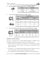
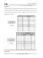
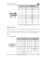
1
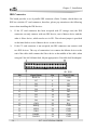
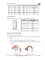
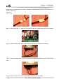
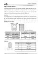
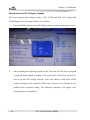
EC7-1813CLD2NA SERIES 基于 Intel® Luna Pier 平台 Mini-ITX 主板 Mini-ITX Motherboard Based on Intel® Luna Pier Platform Version: C00 Copyright Notice Information offered in this manual is believed to be correct at the time of printing, and is subject to change without prior notice in order to improve reliability, design and function and does not represent a commitment on the part of the manufacturer. In no event will the manufacturer be liable for direct, indirect, special, incidental, or consequential damages arising out of improper installation and/or use, or inability to use the product or documentation. This user manual is protected by copyright. No part of this manual may be reproduced, stored in any retrieval system, or transmitted, in any form or by any means, mechanical, electronic, photocopied, recorded or otherwise, without the prior written permission from the manufacturer. Trademarks EVOC is a registered trademark of EVOC Intelligent Technology Co., Ltd. Other product names mentioned herein are used for identification purposes only and may be trademark and/or registered trademarks of their respective companies. Please visit our website: http://www.evoc.com for more information, Or send to the Technical Support Mailbox [email protected] for consultation. [email protected] or Safety Instructions 1. Please read this manual carefully before using the product; 2. Leave the board or card in the antistatic bag until you are ready to use it; 3. Touch a grounded metal object (e.g. for 10 seconds) before removing the board or card from the antistatic bag; 4. Before installing or removing a board, wear the ESD gloves or ESD wrist strap; handle the board by its edges only; 5. Before inserting, removing or reconfiguring motherboards or expansion cards, first disconnect the computer and peripherals from their power sources to prevent electric shock to human bodies or damage to the product; 6. Remember to disconnect the AC power cord from the socket before removing the board or moving the PC; 7. For PC products, remember to disconnect the computer and peripherals from the power sources before inserting or removing a board; 8. Before connecting or disconnecting any terminal, peripheral or any device, be sure the system is powered off and all the power sources are disconnected; 9. After turning off the computer, wait at least 30 seconds before turning it back on Contents Chapter 1 Product Introduction ................................................................................1 Overview.................................................................................................................1 Mechanical Dimensions, Weight and Environment....................................................1 Typical Consumption ...............................................................................................2 Microprocessor........................................................................................................2 Chipset....................................................................................................................2 System Memory ......................................................................................................2 Display Function .....................................................................................................2 Network Function ....................................................................................................3 Audio Function........................................................................................................3 Power Feature..........................................................................................................3 Expansion Bus.........................................................................................................3 Watchdog Function ..................................................................................................3 Operating System ....................................................................................................3 Onboard I/O ...........................................................................................................4 Chapter 2 Installation...............................................................................................5 Product Outline........................................................................................................5 Locations of Connectors ..........................................................................................6 Structure..................................................................................................................7 Jumper Setting.........................................................................................................8 Install the System Memory.......................................................................................9 Serial Port .............................................................................................................10 Display Connector .................................................................................................11 LCD Backlight Control Connector .........................................................................13 Audio Connector ...................................................................................................13 IDE Connector ...................................................................................................... 14 SATA Connector ................................................................................................... 15 Hotswap of SATA Hard Disk................................................................................ 15 KM Connector ...................................................................................................... 17 LAN Port and USB Port ........................................................................................ 18 Parallel Port .......................................................................................................... 19 GPIO Connector.................................................................................................... 19 Power Connector................................................................................................... 20 Status Indicating and Control Connector ................................................................ 21 Fan Connector....................................................................................................... 21 CF Card ................................................................................................................ 22 Expansion Slot ...................................................................................................... 23 Instructions for DVI Display Output ...................................................................... 24 Chapter 3 BIOS Setup ........................................................................................... 27 BIOS Overview..................................................................................................... 27 BIOS Parameter Setup........................................................................................... 27 Basic Function Setting for BIOS ............................................................................ 28 System Resource Managed by BIOS under X86 Platform....................................... 43 Chapter 4 Install the Drivers .................................................................................. 46 Appendix.............................................................................................................. 47 Watchdog Programming Guide .............................................................................. 47 Digital IO Programming Guide.............................................................................. 49 Troubleshooting and Solutions............................................................................... 53 Chapter 1 Product Introduction Chapter 1 Product Introduction Overview The product is an embedded MiniITX single board based on Intel® Luna Pier Refresh platform. The board adopts the technique scheme of Intel® Atom™ D510/D410 processor + Intel® ICH8M onboard. It provides one SODIMM DDR2 slot onboard up to 2GB. It supports three display modes: VGA, 24bit LVDS and DVI; two 10/100/1000M Ethernet controllers; eight USB2.0 ports; two SATA hard disk connectors; one IDE connector, one Type I/II CF connector; one HD Audio connector; six or ten serial ports (one supports RS232/ RS485, two support power supply); one PS/2 KM connector; one PCI slot; the board adopts the standard ATX power supply or 12V single power supply. The product adopts Intel® low power consumption solution and supports multiCOM, power supply on serial port, VGA+LVDS dual display, PCI expansion and so on. It can satisfy the industrial requirements of POS and lottery machines; besides, it can be used in advertising machines, information kiosks, selfservice terminals and other applications which do not require high performance of the motherboard. Mechanical Dimensions, Weight and Environment Ø Dimensions: 170mm (L) x 177.9mm (W) x 41.5mm (H); Ø Net Weight: 0.436 Kg; Ø Operating Environment: Temperature: 10°C ~ 60°C; Humidity: 5% ~ 95% (noncondensing); Ø Storage Environment: Temperature: 40°C ~ 75°C; Humidity: 5% ~ 95% (noncondensing); EC71813CLD2NA SERIES 1 Chapter 1 Product Introduction Typical Consumption The typical consumption is based on the following idle status values. 1. The typical power consumption for EC71813CLD2NAD4V10COM is as follows: CPU: Onboard Intel® Atom™ D410 1.66GHz (166*10/L2=512K) Memory: Transcend DDRII 800 2GB Hard Disk: HITIACH 2TB SATA HDD Ø [email protected]; +5%/3%; 2. The typical power consumption for EC71813CLD2NAD5 is as follows: CPU: Intel® Atom™ D510 Memory: DDRII800 2GB Kingston Hard Disk: Seagate 500GB SATA Ø [email protected]; +5%/3%; Ø [email protected]; +5%/3%; Ø [email protected]; +5%/3%. Microprocessor Intel® Atom™ D510 (Dual Core) /D410 (Single Core) processor onboard, integrated memory controller and graphics controller. Chipset Intel® Atom™D510/D410 processor + Intel® ICH8M System Memory Provides one 200Pin SODIMM DDR2 memory slot, supporting Unbuffered NonECC memory up to 2GB; the memory frequency supported is up to 667MHz. Display Function Ø Adopts CPU with integrated graphics controller; 2 EC71813CLD2NA SERIES Chapter 1 Product Introduction Ø Supports VGA, singlechannel 24bit LVDS and DVI display, among which 24bit LVDS and DVI are homological inputs and the LVDS and DVI are output in Clone mode; supports VGA + LVDS (or DVI) output in Clone or expansion mode; supports three display modes and hotswap function. Ø The maximum resolution and refresh frequency supported by VGA is up to 2048×1536@60Hz while the maximum resolution supported by LVDS is up to 1366×768; The maximum resolution supported by DVI is up to 1600×1200. Network Function Provides two 10/100/1000Mbps LAN ports: LAN1 supports WakeonLAN function while LAN2 supports LAN PXE booting. Audio Function Adopts HD standard, supporting MICIN/LINEIN/LINEOUT. Power Feature Adopts ATX/AT power: ATX power supports ACPI1.0b specification and the status of S0, S1, S4 and S5; AT power supports single 12V power supply. Expansion Bus Provides one PCI slot, complying with PCI 2.3 standard. Watchdog Function Ø 255 levels, programmable by minute or second; Ø Watchdog timeout interrupt or reset system. Operating System Supported OSs: Windows XP, Windows 2000 and Linux. EC71813CLD2NA SERIES 3 Chapter 1 Product Introduction Onboard I/O Ø One parallel port, supporting SSP/EEP/ECP operating modes and BIOS modifies operating mode; Ø Ten serial ports: COM2 supports RS232/RS485 mode selection; COM1 supports Modem wakeup function; COM3 and COM4 support 5V/12V power output; Ø One IDE connector; Ø One CF card connector; Ø Two SATA connectors, supporting hotswap function; Ø Eight USB2.0 ports: USB1 ~ USB4 are brought out via connectors directly; USB5 ~ USB8 are brought out in 2x5Pin headers; Ø Two PS/2 keyboard/mouse connectors: one is a standard connector and the other a pin header; Ø One 8channel digital I/O connector. Tips: how to identify the alarms 1. Long “beep” indicates a system memory error; 2. Short beep indicates to power on the computer. 4 EC71813CLD2NA SERIES Chapter 2 Installation Chapter 2 Installation Product Outline H1 33 H4 170 154.9 132.1 H2 H3 4.9 157.5 170 6.4 Unit: mm Warning! Please adopt appropriate screws and proper installation methods (including board allocation, CPU and heat sink installation, etc); otherwise, the board may be damaged. It is recommended to use M3x6 GB9074.488 screws at H1 ~ H4. EC71813CLD2NA SERIES 5 Chapter 2 Installation Locations of Connectors H1 AUDIO1 J1 J2 J4 AUDIO2 J3 PCI1 JCC1 KM1 COM9 COM7 COM5 COM3 COM10 COM8 COM6 COM4 JP3 JP4 H4 JP5 JP6 JP2 JLCD1 J5 LCDB1 LVDS1 LPT1 GPIO1 J6 KM2 SYSFAN1 CPUFAN1 PWR3 U1 SATA2 PWR2 SATA1 JP1 JCF1 IDE1 PWR1 CF1 H2 FP1 FP2 FP3 DIMM1 6 H3 EC71813CLD2NA SERIES Chapter 2 Installation Structure V GA DB15 D510( DC) / D410( SC) CPU DVI CH A DDR2 S ODIMM1 DDR2 Terminaltion CH7036 LVDS 24BIT DMI S ATA II X2(1*7) USB 2.0 X4 (标 准 ) USB 2.0 X4 (插 针 ) SATA PCIE Por t1 RTL8111D LAN1 RJ45 Conne ctor PCIE Port 2 82574L LAN2 RJ45 Conne ctor USB ICH8M 82801HM I DE1(44pin) CF1(TYPE II) P CI槽 HDA ALC888 SPI SPI Flash SMBus 9534 PATA PCI 内接插针 标准接口 8路 GPIO LPC BUS F81216D IT8782 Ha rdw a re Monitor Pa ra lle l 插 针 PS/2键鼠 外接或 内接 W DT COM1 (RS 232) COM3/4(RS232)插针 第 9PIN 可选RI/5V/12V COM2 (RS 232/485) COM7/ 8/9/10 ( RS232插 针) COM5/6 (RS232)插 针 Tip: How to identify the first pin of the jumpers and connectors 1. Observe the letter beside the socket, it would be marked with “1” or bold lines or triangular symbols; 2. Observe the solder pad on the back; the square pad is the first pin. EC71813CLD2NA SERIES 7 Chapter 2 Installation Jumper Setting 1. JCC1: Clear/Keep CMOS Setting (Pitch: 2.0mm) CMOS is powered by the button battery on board. Clearing CMOS will restore original settings (factory default). The steps are listed as follows: (1) Turn off the computer and unplug the power cable; (2) Instantly short circuit JCC1; (3) Turn on the computer; (4) Follow the prompt on screen to enter BIOS setup when booting the computer, load optimized defaults; (5) Save and exit. Please set as follows: JCC1 2. Setup Function 12 Open Normal (Default) Clear the contents of CMOS and all BIOS settings will restore to factory default values. 12 Short JLCD1: Select LCD Operating Voltage (Pitch: 2.0mm) Different LCD screens have different voltages; the board provides two voltage options, +3.3V and +5V. Only when the selected LCD screen voltage is in accord with the LCD screen operating voltage in use, can the LCD screen operate normally. Please set as follows: JLCD1 3. Setup Function 12 Short +3.3V(Default) 23 Short +5V JCF1: Select CF Card Operating Voltage (Pitch: 2.0mm) Different CF cards have different voltages; the board provides two voltage options, +3.3V and +5V. Only when the selected CF card voltage is in accord with the CF card operating voltage in use, can the system stability be ensured. Please set as follows: JCF1 Setup Function 12 Short +3.3V 23 Short +5V(Default) Note: CF card voltage selection are set to comply with different CF cards; as for the CF cards without specified operating voltages, please choose the operating voltage according to actual usage. 8 EC71813CLD2NA SERIES Chapter 2 Installation 4. JP1: Select Mater and Slave Mode for CF Card (Pitch: 2.0mm) JP1 5. Setup Function 12 Short Master 12 Open Slave(Default) JP2 ~ JP4: Select Mode for Serial Port (Pitch: 2.0mm) Mode Selection Pin Setting RS232 (Default) RS485 JP2 12 34 JP3 12 23 JP4 12 23 JP2 JP3 ~ JP4 6. JP5 ~ JP6: Pin 9 Function Selection for COM3/COM4 (Pitch: 2.0mm) Pin9 Function Selection for COM3/COM4 Pin Setting JP5/JP6 RI#(Default) VCC5V VCC12V JP5 12 34 56 JP6 12 34 56 Install the System Memory The board is configured with one 200Pin DDRII SODIMM slot (DIMM1). When installing the memory bank, please pay attention to the following issues: Ø Open the buckles on both sides of the memory slot. When installing, align the notch of the memory bank with that of the memory slot and gently insert the module into the slot; Ø The memory of 1.8V DDRII 667MHz supported by Intel® Chipset can be used; the maximum memory capacity supported by the board is up to 2GB; Ø It is recommended to use the memory bank with SPD to ensure stable operation. EC71813CLD2NA SERIES 9 Chapter 2 Installation Serial Port The board provides two standard DB9 serial ports: COM1 supports Modem wakeup function and RS232 mode; COM2 supports RS232/RS485 mode selection; it also provides eight 2x5Pin serial ports (Pitch: 2.54mm) of RS232 mode. The pin definitions are as follows: Pin Signal Name 1 DCD# 2 RXD 3 TXD 4 DTR# 5 GND 6 DSR# 7 RTS# 8 CTS# 9 RI# J1(COM1) Pin J1(COM2) Signal Name RS232 RS485 1 DCD# Data 2 RXD Data+ 3 TXD NC 4 DTR# NC 5 GND GND 6 DSR# NC 7 RTS# NC 8 CTS# NC 9 RI# NC Note: the data transmission direction of COM2 is controlled automatically under RS485 mode. 10 EC71813CLD2NA SERIES Chapter 2 Installation COM3 ~ COM10 Pin Signal Name 1 DCD# 2 RXD 3 TXD 4 DTR# 5 GND 6 DSR# 7 RTS# 8 CTS# 9 RI# 10 NA Display Connector The board provides a set of 24bit single channel LVDS connector and one VGA+DVID dual layer connector (Marked as J2 onboard: DVI connector for the upper layer while VGA connector for the lower layer). The pin definitions are as follows: 1. VGA Connector J2(VGA) Pin Signal Name Pin Signal Name 1 Red 2 Green 3 Blue 4 NC 5 GND 6 GND 7 GND 8 GND 9 NC 10 GND 11 NC 12 DDCDATA 13 HSYNC 14 VSYNC 15 DDCCLK EC71813CLD2NA SERIES 11 Chapter 2 Installation 2. DVID Connector Pin Signal Name Pin Signal Name 1 DATA2 13 NC 2 DATA2+ 14 +5V 3 GND_DVI 15 GND 4 NC 16 HOTPLUG 5 NC 17 DATA0 6 DDCCLK 18 DATA0+ 7 DDCDATA 19 GND_DVI 8 NC 20 NC 9 DATA1 21 NC 10 DATA1+ 22 GND_DVI 11 GND_DVI 23 CLK+ 12 NC 24 CLK J2(DVI) 3. Singlechannel 24bit LVDS Connector LVDS1 (Pitch: 1.0mm) Pin Signal Name Pin Signal Name 1 LVDS_D0+ 2 LVDS_D0 3 GND 4 GND 5 LVDS_D1+ 6 LVDS_D1 7 GND 8 GND 9 LVDS_D2+ 10 LVDS_D2 11 GND 12 GND 13 CLK+ 14 CLK 15 GND 16 GND 17 LVDS_D3+ 18 LVDS_D3 19 VDD 20 VDD Note: The LVDS socket adopted by the board is DF20G20DP1V while the corresponding terminal type is DF20A20DF1C. 12 EC71813CLD2NA SERIES Chapter 2 Installation LCD Backlight Control Connector The board provides one 1x4Pin LCD backlight control connector (Pitch: 2.0mm); the pin definitions are as follows: LCDB1 Pin Signal Name 1 VCC_LCDBKLT 2 LCD_BKLTCTL 3 LCD_BKLTEN 4 GND Note: VCC_LCDBKLT+12V backlight power (The current is limited below 1A); LCD_BKLTCTL backlight control (The signal is output as PWM signal via Pineview D; the voltage amplitude is between 0V3.3V while the duty cycle is between 0% ~ 100%); LCD_BKLTEN backlight enable, active high. Audio Connector The board provides one dual layer Audio connector and one 2x5Pin AUDIO pin header. AUDIO1 AUDIO2 (Pitch: 2.0mm) Pin Signal Name 1 LINE_OUT 2 MIC_IN Pin Signal Name Pin Signal Name 1 LOUT_R 2 LOUT_L 3 GND_AUDIO 4 GND_AUDIO 5 LIN_R 6 LIN_L 7 GND_AUDIO 8 GND_AUDIO 9 MIC_L 10 MIC_R EC71813CLD2NA SERIES 13 Chapter 2 Installation IDE Connector The board provides a set of parallel IDE connector (Pitch: 2.0mm), which shares an IDE bus with the CF card connector; therefore, please pay attention to the following issues when installing the IDE devices: Ø If the CF card connector has been occupied with CF storage card, the IDE connector can only connect with one IDE device; one is Master device and the other is Slave device, which can be set via JP1. The relevant jumper is provided on the hard disk to set it to Master device or slave device; Ø If the CF card connector is not occupied, the IDE connector can connect with two IDE devices. The way of connection is to connect the Master device to the end of the cable while connect the Slave device to the middle of the cable; when using an Ultra 66/100 hard disk, 80pin appropriative flat cable shall be adopted. Pin 1 3 5 7 9 11 13 15 17 19 21 23 25 27 29 14 Signal Name RESET# D7 D6 D5 D4 D3 D2 D1 D0 GND DREQ IOW# IOR# IORDY DACK# Pin 2 4 6 8 10 12 14 16 18 20 22 24 26 28 30 IDE1 Signal Name GND D8 D9 D10 D11 D12 D13 D14 D15 Key GND GND GND GND GND EC71813CLD2NA SERIES Chapter 2 Installation 31 33 35 37 39 41 43 IRQ DA1 DA0 CS1# LED# +5V GND 32 34 36 38 40 42 44 NC ATA66_DET DA2 CS3# GND +5V GND SATA Connector The board provides two SATA sockets; the pin definitions are as follows: SATA1/SATA2 Pin Signal Name 1 GND 2 TX+ 3 TX 4 GND 5 RX 6 RX+ 7 GND Hotswap of SATA Hard Disk Notices for hotswap of SATA hard disk: 1. The hard disk shall support SATA 2.0 and use 15pin SATA hard disk power connector. 2. The driver of chipset shall support the hotswap of SATA hard disk. 3. Hotswap of SATA hard disk with the operating system is forbidden when system is poweredon. SATA Data Cable SATA Power Cable EC71813CLD2NA SERIES 15 Chapter 2 Installation Please carry out hot plug as follows, improper operation may destroy the hard disk or result in data lost. Hot Plug Step 1: Please plug the 1 x 4 pin SATA power connector (white) into the power adapter. Step 2: Please connect the SATA data cable to the SATA connector on board. Step 3: Please connect the 15pin SATA power connector (black) to the SATA hard disk. Step 4: Please connect the SATA data cable to the SATA hard disk. 16 EC71813CLD2NA SERIES Chapter 2 Installation Hot Unplug Step 1: Uninstall the hard disk from the device manager. Step 2: Unplug the data cable from the SATA hard disk. Step 3: Unplug the SATA 15pin power connector (black) from the SATA hard disk. KM Connector The board provides one standard PS/2 KM combined connector and one KM pin header (Pitch: 2.0mm). KM1 KM2 Pin Signal Name Pin Signal Name 1 KB_DATA 7 MS_DATA 2 NC 8 NC 3 GND 9 GND 4 +5V 10 +5V 5 KB_CLK 11 MS_CLK 6 NC 12 NC Pin Signal Name Pin Signal Name 1 KB_DATA 2 MS_DATA 3 KB_CLK 4 MS_CLK 5 GND 6 GND 7 +5V 8 +5V EC71813CLD2NA SERIES 17 Chapter 2 Installation LAN Port and USB Port The board provides two LAN ports and eight USB ports, among which one LAN port and two USB ports share a set of socket (i.e. J3 and J4 include one LAN port and two USB ports, respectively). In addition, the board also provides two 2x5 Pin USB connectors, (J5 and J6), which can connect with four USB devices. LAN Port The board provides two 10/100/1000Mbps Ethernet connectors. ACTLED and LILED are the LED indicators beside the Ethernet port, which respectively indicates the activity status and the transmission status of LAN. Please refer to the status description for each LED: J3(LAN1)/J4(LAN2) LILED (DualColor: O/G) LAN Speed Indicator Green 1000Mbps Data Transmitting Orange 100Mbps No Data to Transmit Off 10Mbps ACTLED (Green) LAN Activity Status Indicator Blink Off USB Port J3(USB1/USB2) J4(USB3/USB4) 18 Pin Signal Name 1 +5V 2 USB_Data 3 USB_Data+ 4 GND EC71813CLD2NA SERIES Chapter 2 Installation J5(USB5/USB6) J6(USB7/USB8) Pitch: 2.54mm Pin Signal Name Pin Signal Name 1 +5V 2 +5V 3 USB1_Data 4 USB2_Data 5 USB1_Data+ 6 USB2_Data+ 7 GND 8 GND 9 NA 10 GND Parallel Port The board provides one 2x13Pin parallel port (Pitch: 2.0mm). LPT1 Pin Signal Name Pin Signal Name 1 STB# 2 AFD# 3 PD0 4 ERR# 5 PD1 6 INIT# 7 PD2 8 SLIN# 9 PD3 10 GND 11 PD4 12 GND 13 PD5 14 GND 15 PD6 16 GND 17 PD7 18 GND 19 ACK# 20 GND 21 BUSY 22 GND 23 PE 24 GND 25 SLCT 26 NC GPIO Connector The board provides one 2x5Pin GPIO pin header (Pitch: 2.0mm). EC71813CLD2NA SERIES 19 Chapter 2 Installation 1 Signal Name GPIO1 2 Signal Name GPIO5 3 GPIO2 4 GPIO6 5 GPIO3 6 GPIO7 7 GPIO4 8 GPIO8 9 GND 10 NC Pin GPIO1 Pin Note: the pins on GPIO are bidirectional signals. To facilitate test and application, the factory default value is that Pin 1, 3, 5, and 7 are for input while Pin 2, 4, 6 and 8 are for output. Power Connector 1) AT Power Connector: 12V Single Power Connector (Pitch: 4.2mm) PWR2 2) Signal Name 1 GND 2 GND 3 +12V 4 +12V ATX Power Connector (Pitch: 4.2mm) PWR1 20 Pin Pin Signal Name Pin Signal Name 1 +3.3V 11 +3.3V 2 +3.3V 12 12V 3 GND 13 GND 4 +5V 14 PS_ON# 5 GND 15 GND 6 +5V 16 GND 7 GND 17 GND 8 PWROK 18 5V 9 +5VSB 19 +5V 10 +12V 20 +5V EC71813CLD2NA SERIES Chapter 2 Installation 3) SATA Power Connector (Pitch: 5.08mm) Pin Signal Name 1 +12V 2 GND 3 GND 4 +5V PWR3 Status Indicating and Control Connector 1) ATX Power Switch and HDD Indicator Connector (Pitch: 2.54mm) Signal Name PWRBTN# Pin Signal Name 2 GND 3 GND 4 RESET# 5 HDD_LED 6 HDD_LED+ Pin 1 FP1 2) Power Indicator Connector (Pitch: 2.54mm) FP2 3) Pin Signal Name 1 PWR_LED+ 2 NC 3 GND Loudspeaker Output Connector (Pitch: 2.54mm) FP3 Pin Signal Name 1 SPEAKER 2 NC 3 4 GND +5V Fan Connector The board provides two 1x3Pin fan connectors (Pitch: 2.54mm). CPUFAN1/SYSFAN1 Pin Signal Name 1 GND 2 +12V 3 FAN_IO FAN_IO: fan speed impulse output. EC71813CLD2NA SERIES 21 Chapter 2 Installation CF Card Marked as CF1 onboard. Pin Signal Name Pin Signal Name 1 GND 26 CD1# 2 D3 27 D11 3 D4 28 D12 4 D5 29 D13 5 D6 30 D14 6 D7 31 D15 7 CS0# 32 CS1# 8 GND 33 VS1# 9 ATASEL# 34 IOR# 10 GND 35 IOW# 11 GND 36 WE# 12 GND 37 IRQ 13 VCC 38 VCC 14 GND 39 CSEL# 15 GND 40 VS2# 16 GND 41 RESET# 17 GND 42 IORDY 18 A2 43 DREQ 19 A1 44 DACK# 20 A0 45 DASP# 21 D0 46 ATA66_DET 22 D1 47 D8 23 D2 48 D9 24 WP/IOCS16# 49 D10 25 CD2# 50 GND 22 EC71813CLD2NA SERIES Chapter 2 Installation Expansion Slot PCI slot is used as the standard PCI (version 2.3) connector (PCI1); the pin definitions are as follows: Pin Signal Name Pin Signal Name Pin Signal Name Pin Signal Name A1 TRST# A31 PCI_AD18 B1 12V B31 +3.3V A2 +12V A32 PCI_AD16 B2 TCK B32 PCI_AD17 A3 TMS A33 +3.3V B3 GND B33 PCI_C/BE#2 A4 TDI A34 PCI_FRAME# B4 TDO B34 GND A5 +5V A35 GND B5 +5V B35 PCI_IRDY# A6 INTA# A36 PCI_TRDY# B6 +5V B36 +3.3V A7 INTC# A37 GND B7 INTB# B37 PCI_DEVSEL# A8 +5V A38 PCI_STOP# B8 INTD# B38 GND A9 Null A39 +3.3V B9 PRSNT1# B39 PCI_PLOCK# A10 +5V A40 SMCLK B10 Null B40 PCI_PERR# A11 Null A41 SMDATA B11 PRSNT2# B41 +3.3V A12 GND A42 GND B12 GND B42 PCI_SERR# A13 GND A43 PCI_PAR B13 GND B43 +3.3V A14 3.3Vaux A44 PCI_AD15 B14 Null B44 PCI_C/BE#1 A15 PCI_RST# A45 +3.3V B15 GND B45 PCI_AD14 A16 +5V A46 PCI_AD13 B16 PCI_CLK B46 GND A17 PCI_GNT# A47 PCI_AD11 B17 GND B47 PCI_AD12 A18 GND A48 GND B18 PCI_REQ# B48 PCI_AD10 A19 PCI_PME# A49 PCI_AD9 B19 +5V B49 GND A20 PCI_AD30 A50 PCI_C/BE#0 B20 PCI_AD31 B50 PCI_AD8 A21 +3.3V A51 +3.3V B21 PCI_AD29 B51 PCI_AD7 A22 PCI_AD28 A52 PCI_AD6 B22 GND B52 +3.3V A23 PCI_AD26 A53 PCI_AD4 B23 PCI_AD27 B53 PCI_AD5 A24 GND A54 GND B24 PCI_AD25 B54 PCI_AD3 A25 PCI_AD24 A55 PCI_AD2 B25 +3.3V B55 GND A26 PCI_IDSEL A56 PCI_AD0 B26 PCI_C/BE#3 B56 PCI_AD1 A27 +3.3V A57 +5V B27 PCI_AD23 B57 +5V A28 PCI_AD22 A58 PCI_REQ64# B28 GND B58 PCI_ACK64# A29 PCI_AD20 A59 +5V B29 PCI_AD21 B59 +5V A30 GND A60 +5V B30 PCI_AD19 B60 +5V Note: when adopting PWR2 to supply power, Pin B1 is NC. EC71813CLD2NA SERIES 23 Chapter 2 Installation Instructions for DVI Display Output The board supports three display modes: VGA, LVDS and DVI; DVI display and LVDS display are Clone mode. Please set as follows: 1. Enter the BIOS menu to set the DVI display mode as shown in the figure below: 2. After installing the operating system for the first time, the DVI driver program is required; please install according to the enclosed CD. The driver can only be used to set the DVI display function. Users may choose 18bit/24bit LVDS output according to the connected LVDS screen. Please refer to Readme.txt for detailed driver program setting. The following interfaces will appear after completing driver installation: 24 EC71813CLD2NA SERIES Chapter 2 Installation 3. Set the resolution for DVI. After the motherboard reads the resolution supported by the display, the resolution supported by the display will be shown. Please refer to the figure below: EC71813CLD2NA SERIES 25 Chapter 2 Installation 4. Set the display dimensions of the DVI, DVI displays the extendable screen dimensions. Please refer to the figure below: 5. After setting the driver, the parameters are restored. It will display by the same configuration next time. 6. DVI display function is realized via CH7036A, which shall abide by the following suggestions: 1. The output resolution for DVI shall be no less than that of the LVDS set in the BIOS menu; if the output resolution for DVI is less than that of the LVDS, the fonts displayed under certain frequency might be blurred. 2. If the background color is set to pale blue, then erect stripes might appear under certain frequency; which is caused by the implementation mechanism of CH7036A and is normal. 26 EC71813CLD2NA SERIES Chapter 3 BIOS Setup Chapter 3 BIOS Setup BIOS Overview BIOS (Basic Input and Output System) is solidified in the flash memory on the CPU board. Its main functions include: initialize system hardware, set the operating status of the system components, adjust the operating parameters of the system components, diagnose the functions of the system components and report failures, provide hardware operating and controlling interface for the upper level software system, guide operating system and so on. BIOS provides users with a humancomputer interface in menu style to facilitate the configuration of system parameters for users, control power management mode and adjust the resource distribution of system device, etc. Setting the parameters of the BIOS correctly could enable the system operating stably and reliably; it could also improve the overall performance of the system at the same time. Inadequate even incorrect BIOS parameter setting will decrease the system operating capability and make the system unstable or even unable to operate normally. BIOS Parameter Setup Prompt message for BIOS setting may appear once the system is powered on. At that time (invalid at other time), press the key specified in the prompt message (usually <Del>) to enter BIOS setting. When the BIOS setting in CMOS is destroyed, system may also require entering BIOS setting or selecting certain default value. All the setup values modified by BIOS are saved in the CMOS storage in system. The CMOS storage is powered by battery; unless clearing CMOS is executed, its contents would not be lost even if powered off. Note! BIOS setting will influence the computer performance directly. Setting parameter improperly will cause damage to the computer; it may even be unable to power on. Please use the internal default value of BIOS to restore the system. Our company is constantly researching and updating BIOS, its setup interface may be a bit different. The figure below is for reference only; it may be different from your BIOS setting in use. EC71813CLD2NA SERIES 27 Chapter 3 BIOS Setup Basic Function Setting for BIOS After starting SETUP program, the main interface of CMOS Setup Utility will appear: BIOS SETUP UTILITY System Overview Processor Type : Intel(R) Atom(TM) CPU K510 @ 1.66GHz Speed :1666MHz Cores :2 ←→ Select Screen ↑↓ Select Item + Change Field Tab Select Field F1 General Help F10 Save and Exit ESC Exit System Memory Size :1015MB System Time System Date [00:47:55] [Mon 01/11/2010] V02.57 (c)Copyright 19852004,American Megatrends, Inc. u Main Ø System Time Choose this option and set the current time by < + > / < >, which is displayed in the format of hour/minute/second. Reasonable range for each option is: Hour (0023), Minute (0059), Second (0059). Ø System Date Choose this option and set the current date by < + > / < >, which is displayed in the format of month/date/year. Reasonable range for each option is: Month (Jan.Dec.), Date (0131), Year (Maximum to 2099), Week (Mon. ~ Sun.). 28 EC71813CLD2NA SERIES Chapter 3 BIOS Setup u Advanced BIOS SETUP UTILITY Configure CPU Advanced Settings WARNING: Setting wrong values in below sections may cause system to malfunction „CPU Configuration „IDE Configuration „Super I/O Configuration „Hardware Health Configuration „USB Configuration „Power Management Configuration „Clock Generator Configuration ←→ Select Screen ↑↓ Select Item Enter Go to Sub Screen Tab Select Field F1 General Help F10 Save and Exit ESC Exit V02.57 (c)Copyright 19852004, American Megatrends, Inc. Ø CPU Configuration BIOS SETUP UTILITY Configure advanced CPU settings Brand String: Intel(R) Atom(TM) CPU K510 @ 1.66GHz Frequency; :1.66GHz FSB Speed; :667MHz Cache L1; :48 KB Cache L2; :1024 KB Ratio Actual Value :10 Hyper Threading Technology [Enabled] Intel(R) SpeedStep(tm) tech [Enabled] ←→ Select Screen ↑↓ Select Item + Change Field Tab Select Field F1 General Help F10 Save and Exit ESC Exit V02.57 (c)Copyright 19852004, American Megatrends, Inc EC71813CLD2NA SERIES 29 Chapter 3 BIOS Setup l Hyper Threading Technology Control switch for the Intel Hyper Threading Technology function. l Intel(R) SpeedStep(tm) tech Control switch for the Intel(R) SpeedStep(tm) tech function. Ø IDE Configuration BIOS SETUP UTILITY IDE Configuration ATA/IDE Configuration Configure SATA as [Enhanced] [IDE] „Primary IDE Master :[Not Detected] „Primary IDE Slave :[Not Detected] „Secondary IDE Master :[Not Detected] „Secondary IDE Slave :[Not Detected] „Third IDE Master :[Not Detected] „Third IDE Slave :[Not Detected] ←→ Select Screen ↑↓ Select Item + Change Field Tab Select Field F1 General Help F10 Save and Exit ESC Exit V02.57 (c)Copyright 19852004, American Megatrends, Inc. l ATA/IDE Configuration This option is used to configure the operating mode for ATA; there are two options: Enhanced and Compatible. l Configure SATA as SATA controller type selection; there are two options for this item: IDE and AHCI. Only when the ATA/IDE Configuration is under Enhanced mode, is AHCI supported. The AHCI function requires supports from hardware chip and OS. l Legacy IDE Channels 30 EC71813CLD2NA SERIES Chapter 3 BIOS Setup Configure the IDE channel type under Compatible mode; there are four options: SATA Only, SATA Pri, PATA Sec and PATA Only. l Primary ~ Third IDE Master/Slave ﹡Type Not Installed: no IDE device can be detected by system; AUTO: automatic detection of IDE parameters when powering on; CD/DVD: used for ATAPI CDROM; ARMD: used for various analog IDE devices. ﹡LBA/Large Mode Used to set whether to support LBA mode or not. ﹡Block(Multisector Transfer) Used to set whether to support multisector simultaneous transfer or not. ﹡PIO Mode Used for PIO mode setting. ﹡DMA Mode Used for DMA mode setting. ﹡S.M.A.R.T Used to set whether to enable S.M.A.R.T function and it is only available for the hard disk supporting this function. ﹡32Bit Data Transfer This option is used to enable the 32bit hard disk accessing mode, which could optimize hard disk read and write speed. l AHCI Port0 ~ 2 AHCI configuration menu, which is displayed only when the SATA controller is configured as AHCI or RAID. ﹡SATA Port0 ~ 2 Auto: automatic detection of SATA device when powering on; Not Installed: disable the port without inspection. ﹡S.M.A.R.T Used to set whether to enable S.M.A.R.T function and it is only available for the hard disk supporting this function. EC71813CLD2NA SERIES 31 Chapter 3 BIOS Setup Ø Super I/O Configuration BIOS SETUP UTILITY Configure Super I/O Chipset OnBoard Floppy Controller [Enabled] Serial Port1 Address [3F8] Serial Port1 IRQ [4] Serial Port2 Address [2F8] Serial Port2 IRQ [4] Serial Port3 Address [3E8] Serial Port3 IRQ [3] Serial Port4 Address [2E8] Serial Port4 IRQ [3] Serial Port5 Address [2F0] Serial Port5 IRQ [10] Serial Port6 Address [2E0] Serial Port6 IRQ [10] Serial Port7 Address [200] Serial Port7 IRQ [11] Serial Port8 Address [208] Serial Port8 IRQ [11] Serial Port9 Address [210] Serial Port9 IRQ [11] Serial Port10 Address [218] Serial Port10 IRQ [11] Parallel Port Address [378] Parallel Port Mode [Normal] Parallel Port IRQ [IRQ7] Uart IRQ Attribute Allows BIOS to Enable or Disable Floppy Controller. ←→ Select Screen ↑↓ Select Item + Change Field Tab Select Field F1 General Help F10 Save and Exit ESC Exit [Edge Active High] V02.57 (c)Copyright 19852004, American Megatrends, Inc. 32 EC71813CLD2NA SERIES Chapter 3 BIOS Setup l OnBoard Floppy Controller Used to enable the floppy driver controller. l Serial Port n Address Set the addresses of the serial port n on motherboard (n=1…10). l Serial Port n IRQ Set the IRQs of the serial port n on motherboard (n=1…10). l Parallel Port Address Set the addresses of the parallel port on motherboard; the default value is 378. l Parallel Port Mode Set the modes for the parallel port on motherboard. l Parallel Port IRQ Set the IRQs of the parallel port on motherboard. l Uart IRQ Attribute Set the IRQ attribute for COM 710. EC71813CLD2NA SERIES 33 Chapter 3 BIOS Setup Ø Hardware Health Configuration BIOS SETUP UTILITY Hardware Health Configuration System Temperature : 30℃/86℉ CPU Temperature : 37℃/98℉ Enables Hardware Health Monitoring Device SYSFAN1 CPUFAN1 Vcore : 1.136 V V3.3 : 3.296 V V5.0 : 5.094 V V12.0 : 12.196 V VBAT : 3.152 V ←→ Select Screen ↑↓ Select Item + Change Field Tab Select Field F1 General Help F10 Save and Exit ESC Exit V02.57 (c)Copyright 19852004, American Megatrends, Inc. l System Temperature Current system temperature, it is monitored by thermal resistor on motherboard. l CPU Temperature Current CPU temperature, it is monitored by temperature sensors on motherboard. l Vcore CPU core voltage; l V3.3/ V5.0/ V12.0 Turn on/off power to output voltage. l VBAT Monitor the battery voltage. 34 EC71813CLD2NA SERIES Chapter 3 BIOS Setup Ø USB Configuration BIOS SETUP UTILITY Enables USB host controllers. USB Configuration USB Devices Enabled: 1 Keyboard, 1 Drive USB Function USB 2.0 Controller [8 USB Ports] [Enabled] Legacy USB Support [Auto] „USB Mass Storage Device Configuration ←→ Select Screen ↑↓ Select Item + Change Field F1 General Help F10 Save and Exit ESC Exit V02.57 (c)Copyright 19852004, American Megatrends, Inc. l USB Function This option sets the amount of USB controller; that is to confirm how many USB controllers are supported. One controller usually supports two USB ports. l USB 2.0 Controller This option is used to select whether to support USB 2.0 controller. l Legacy USB Support This option is used to support legacy USB devices (such as keyboard, mouse and storage devices, etc); when this option is set to Enabled, the USB device could be used even if under OS that doesn’t support USB, such as DOS. l USB Mass Storage Device Configuration This option is used to configure the USB mass storage device, including Reset delay setting and enumeration type. EC71813CLD2NA SERIES 35 Chapter 3 BIOS Setup Ø Power Management Configuration BIOS SETUP UTILITY Power Management Configuration ACPI APIC Support [Enabled] Restore on AC Power Loss [Last state] Resume on RTC Alarm [Disabled] ←→ Select Screen ↑↓ Select Item + Change Field F1 General Help F10 Save and Exit ESC Exit V02.57 (c)Copyright 19852004, American Megatrends, Inc. l ACPI APIC Support This option is used to enable or disable APIC under ACPI OS. l Restore on AC Power Loss This option could set the system status when the computer is reelectrified after powered off under AC. “Power Off” is to make the system at power off status; “Power On” is to power on the system automatically; “Last State” is to recover the status before powering off. l Resume on RTC Alarm This option is used to enable or disable the system clock. When the specified time expires, it will wake the system from power saving mode, even from power off mode. This function shall be supported by ATX power. 36 EC71813CLD2NA SERIES Chapter 3 BIOS Setup Ø Clock Generator Configuration BIOS SETUP UTILITY Configure Clock Generator Spread Spectrum [Enabled] Auto PCI Clock [Enabled] ←→ Select Screen ↑↓ Select Item + Change Field F1 General Help F10 Save and Exit ESC Exit V02.57 (c)Copyright 19852004, American Megatrends, Inc. l Spread Spectrum This option is used to control the spread spectrum function of the clock signal. l Auto PCI Clock This option is used to detect the devices on PCI slot automatically. If there are no devices in the slot, please disable the clock signal on that slot. EC71813CLD2NA SERIES 37 Chapter 3 BIOS Setup u Chipset BIOS SETUP UTILITY Advanced Chipset Settings WARNING: Setting wrong values in sections below may cause system to malfunction. North Bridge Chipset Configuration DRAM Frequency [Auto] ←→ Select Screen ↑↓ Select Item [PCI/IGD] Enter Go to Sub [CRT+LVDS] Screen [24BIT] F1 General Help [800x600/S/18/G104S] F10 Save and Exit ESC Exit [Disabled] Configure DRAM Timing by SPD [Enabled] Initiate Graphic Adapter Boot Display Device LVDS Color Depth Flat Panel Type UserDefine Panel Type South Bridge Chipset Configuration PXE Boot [Disabled] Onboard Audio Controller [Enabled] V02.57 (c)Copyright 19852004, American Megatrends, Inc. Ø DRAM Frequency Configure the frequency for DRAM; it is recommended to use automatic modification instead of manual modification; otherwise, it will not be able to power on because it is not supported by DRAM. Ø Configure DRAM Timing by SPD BIOS configures the time sequence of the SDRAM according to the contents of the SPD chip. Most of the memory bank has one small chip to save the time sequence and capacity of the memory, i.e. the SPD chip. Ø Initiate Graphic Adapter This option is used to specify the bootup priority of the video device type. Ø Boot Display Device This option is used to select the default display device when booting. 38 EC71813CLD2NA SERIES Chapter 3 BIOS Setup Ø LVDS Color Depth This option is used to select the color depth of LVDS. Ø Flat Panel Type This option is used to select the resolution for Flat Panel. Ø UserDefine Panel Type Configure the flat panel display type according to user definition. Ø PXE Boot This option is used to select whether to enable LAN PXE boot function. Ø Onboard Audio Controller Select whether to enable the audio card controller. u PCIPnP BIOS SETUP UTILITY Advanced PCI/PnP Settings WARNING: Setting wrong values in below sections may cause system to malfunction. IRQ3 [Available] IRQ4 [Available] IRQ5 [Available] IRQ7 [Available] IRQ9 [Available] IRQ10 [Available] IRQ11 [Available] IRQ14 [Available] IRQ15 [Available] ←→ Select Screen ↑↓ Select Item + Change Field F1 General Help F10 Save and Exit ESC Exit V02.57 (c)Copyright 19852004, American Megatrends, Inc. Ø IRQ3 ~ 15 This option is used to specify whether the IRQ number is PNP mode or reserved for ISA. EC71813CLD2NA SERIES 39 Chapter 3 BIOS Setup u Boot BIOS SETUP UTILITY Boot Settings Quick Boot [Enabled] Quiet Boot [Disabled] Waite For ‘F1’ If Error [Enabled] Boot Device Priority Boot from Embedded WinCE st 1 Boot Device ←→ Select Screen ↑↓ Select Item Enter Go to Sub Screen F1 General Help F10 Save and Exit ESC Exit [No] [USB: aigo USB DISK] V02.57 (c)Copyright 19852004, American Megatrends, Inc. Ø Quick Boot During BIOS booting period, configure whether to permit skipping certain test to reduce BIOS booting time. Ø Quiet Boot Configure whether to display the content of OEM LOGO. Ø Wait For ‘F1’ If Error Configure whether to prompt pressing “F1” during system error. Ø Boot from Embedded WinCE Configure to boot from WinCE system. Ø 1 st ~ 4 th Boot Device Configure the priority of the boot sequence for devices when the system boots. 40 EC71813CLD2NA SERIES Chapter 3 BIOS Setup u Security BIOS SETUP UTILITY Security Settings Supervisor Password :Not Installed User Password :Not Installed Change Supervisor Password Change User Password Install or Change the password ←→ Select Screen ↑↓ Select Item Enter Change F1 General Help F10 Save and Exit ESC Exit V02.57 (c)Copyright 19852004, American Megatrends, Inc. Ø Change User/ Supervisor Password After pressing Change User/ Supervisor Password and input new password in the dialog box, this column will indicate that user’s password has been installed. u Exit South Bridge Configuration Exit Options Save Changes and Exit Discard Changes and Exit Discard Changes Load Optimal Defaults Exit system setup after saving the changes. ←→ Select Screen ↑↓ Select Item Enter Go to Sub Screen F1 General Help F10 Save and Exit ESC Exit Load Failsafe Defaults V02.57 (c)Copyright 19852004, American Megatrends, Inc. EC71813CLD2NA SERIES 41 Chapter 3 BIOS Setup Ø Save Changes and Exit When you have finished all the changes and want to cover the original parameters, you may implement this operation and save the new parameters into CMOS storage. To implement this operation, you may choose this option and press < Enter >; press < Enter > again to exit. Ø Discard Changes and Exit If you do not want to save the change into CMOS storage, please choose this option and press < Enter >; press < Enter > again to exit. Ø Discard Changes If error occurs in your change and the changes need to be neglected, please choose this option and press < Enter > in order to enter corresponding options again and reset it. Ø Load Optimal Defaults This menu is used to input default value in system configuration. These default values are optimized and could give play to the high capability of all hardware. Ø Load Failsafe Defaults The function of this option is to initialize the setup of each option to realize the most fundamental and secure system functional value. To implement this function, choose this option and press < Enter >; messages to be confirmed will be shown on the screen, press < Enter > to implement this function. 42 EC71813CLD2NA SERIES Chapter 3 BIOS Setup System Resource Managed by BIOS under X86 Platform We define three kinds of system resources here: I/O port address, IRQ interrupt number and DMA number. u DMA Level u Function DMA0 DRAM Refresh DMA1 Unassigned DMA2 Unassigned DMA3 Unassigned (sometimes used for hard disk) DMA4 Used for DMAC Cascade DMA5 Unassigned DMA6 Unassigned DMA7 Unassigned APIC Advanced programmable interrupt controller. Most motherboards above P4 level support APIC and provide more than 16 interrupt sources, like IRQ16 IRQ23; while some others can have up to 28 interrupt sources, such as motherboard supporting PCIX. However, relevant OS are required to enable that function, and currently, only the OS above Windows 2000 could support that function. u IO Port Address There is 64K for the system I/O address space. Each peripheral will occupy portion of the space. The table below shows parts of the distribution of the I/O address. As the address of PCI device (e.g. PCI network card) is configured by software, it is not listed in this table. EC71813CLD2NA SERIES 43 Chapter 3 BIOS Setup Address 000h 00Fh DMA Controller #1 020h 021h Programmable Interrupt Controller #1 040h 043h System Timer 060h 064h Standard 101/102 Keyboard Controller 070h 071h Real Time Clock, NMI 080h 09Fh DMA Page Register 0A0h 0A1h Programmable Interrupt Controller #2 0C0h 0DFh DMA Controller #2 0F0h – 0FFh Numeric Data Processor 1F0h 1F7h Primary IDE Channel 200h – 207h COM7 208h – 20Fh COM8 210h – 217h COM9 218h – 21Fh COM10 274h – 279h, A79h 44 Device Description PnP Configuration Register 2E0h – 2E7h COM6 2E8h – 2EFh COM4 2F0h – 2F7h COM5 2F8h 2FFh COM2 378h 37Fh LPT1 3B0h – 2BBh Intel(R) Graphics Media Accelerator 3150 3C0h – 2DFh Intel(R) Graphics Media Accelerator 3150 3E8h – 3EFh COM3 3F6h 3F6h Primary IDE Channel 3F8h 3FFh COM1 400h– 41Fh SMBus Controller EC71813CLD2NA SERIES Chapter 3 BIOS Setup u IRQ Assignment Table There are 15 interrupt sources of the system. Some are occupied by the system devices. Only the ones that are not occupied can be distributed. The ISA devices claim to engross the interrupt. Only the plug and play ISA devices can be distributed by the BIOS or the OS. And several PCI devices share one interrupt through the distribution of BIOS or OS. The diagram below shows parts of the interrupt distribution under X86 platform, but it does not show the interrupt source occupied by the PCI devices. Level Function IRQ0 System Timer IRQ1 Standard 101/102 Key or Microsoft Keyboard IRQ2 Programmable Interrupt Controller IRQ3 COM#3#4 IRQ4 COM#1#2 IRQ5 Reserved IRQ6 Reserved for FDD controller IRQ7 Parallel Port IRQ8 System CMOS/Real Time Clock IRQ9 ACPI IRQ10 COM#5#6 IRQ11 COM#7#10 IRQ12 PS/2 Mouse IRQ13 Numeric Data Processor IRQ14 Primary IDE IRQ15 Reserved EC71813CLD2NA SERIES 45 Chapter 4 Install the Drivers Chapter 4 Install the Drivers Regarding the driver program of this product, please refer to the accompanying CD. 46 EC71813CLD2NA SERIES Appendix Appendix Watchdog Programming Guide The board provides a programmable watchdog timer (WDT) up to 255 levels and timed by minute or second. Watchdog timeout event can be programmed to reset system or generate maskable interrupts. The available IRQ numbers for this board are: 3, 4, 5, 7, 9, 10 and 11. Please modify the corresponding IRQ number in PCIPnP of BIOS Setup interface into “Reserved” before using. The following describes WDT program in C language. The steps to program WDT are listed as follows: Ø Enter WDT programming mode; Ø Set WDT operating mode, enable WDT/disable WDT. (1) Enter WDT Programming Mode #define INDEX_PORT 0x2E #define DATA_PORT 0x2F outportb(INDEX_PORT,0x87); outportb(INDEX_PORT,0x01); outportb(INDEX_PORT,0x55); outportb(INDEX_PORT,0x55); outportb(INDEX_PORT,0x07); outportb(DATA_PORT,0x07); (2) Set WDT operating mode, reset mode or interrupt mode: a. Configure WDT to reset mode outportb(INDEX_PORT,0x72) outportb(DATA_PORT,00); outportb(INDEX_PORT,0x72); int val=inportb(DATA_PORT); EC71813CLD2NA SERIES 47 Appendix val |=0x40; outportb(DATA_PORT, val); b. Configure WDT to interrupt mode outportb(INDEX_PORT,0x72) outportb(DATA_PORT,IRQ_ NO); /*Please replace the constant IRQ_NO with the interrupt number need to be used. The available range of the interrupt number has been listed in the beginning of this chapter*/ outportb(INDEX_PORT,0X72); int val=inportb(DATA_PORT); val&=0xBF; outportb(DATA_PORT, val); (3) Configure WDT to time by minute or second: a. Time by minute: val &=0x7f; outportb(INDEX_PORT, 0x72); outportb(DATA_PORT, val); b. Time by second: val |=0x80; outportb(INDEX_PORT,0x72); outportb(DATA_PORT, val); (4) Enable/disable WDT a. Enable WDT: outportb(INDEX_PORT,0x73); outportb(DATA_PORT,TIME_OUT_VALUE); /*Please replace the constant TIME_OUT_VALUE with the unit number of timeout value (0x01 ~ 0xFF)*/ b. Disable WDT: outportb(INDEX_PORT,0xf6); outportb(DATA_PORT,0x00); 48 EC71813CLD2NA SERIES Appendix Digital IO Programming Guide The board provides 16channel programmable digital IO pins, eight for input while the other eight for output. The following provides digital I/O program in C language; please follow the steps below to implement digital I/O programming: Ø Initialize digital I/O Ø Input/output program (1) Initialize digital I/O: #define BAR 0x400 unsigned char tmp_val; outportb(BAR,0xbf); outportb(BAR+0x04,0x40); outportb(BAR+0x03,0x03); outportb(BAR+0x05,0x0f); tmp_val =(inportb(BAR+0x02)|0x08)&0xeb; tmp_val |= 0x40; outportb(BAR+0x02, tmp_val); delay(30); tmp_val =inportb(BAR); while((tmp_val &0x02)!=0x02) { tmp_val =inportb(BAR); if((tmp_val &0x04)!=0) { printf("ERROR\n"); return 0; } } outportb(BAR,0xbf); outportb(BAR+0x04,0x42); outportb(BAR+0x03,0x03); EC71813CLD2NA SERIES 49 Appendix outportb(BAR+0x05,0x0f); tmp_val =(inportb(BAR+0x02)|0x08)&0xeb; tmp_val |= 0x40; outportb(BAR+0x02, tmp_val); delay(30); tmp_val =inportb(BAR); while((tmp_val &0x02)!=0x02) { tmp_val =inportb(BAR); if((tmp_val &0x04)!=0) { printf("ERROR\n"); return 0; } } (2) Input/output program: a. Output Program Functions input: int pin Value 1 ~ 8 are corresponding with output pin 1 ~ 8 int lev_val 1 is to output high level; 0 is to output low level Functions Output: none void Out_Lev(int pin ,int lev_val) { unsigned int reg_val ; outportb(BAR,0xbf); if(pin < 5) { outportb(BAR+0x04,0x40); } else { 50 EC71813CLD2NA SERIES Appendix outportb(BAR+0x04,0x42); pin = pin – 4; } outportb(BAR+0x03,0x01); reg_val = inportb(BAR+0x05); reg_val = lev_val ? reg_val|(0x01<<pin1) :reg_val&(~(0x01<<pin1)) ; outportb(BAR+0x05, reg_val); reg_val =(inportb(BAR+0x02)|0x08)&0xeb; reg_val |= 0x40; outportb(BAR+0x02, reg_val); delay(30); reg_val =inportb(BAR); while((reg_val &0x02)!=0x02) { reg_val =inportb(BAR); if((reg_val &0x04)!=0) { printf("ERROR\n"); return 0; } } } b. Input Program Functions Input: int pin Value 1 ~ 8 are corresponding with the input pin 1 ~ 8 Functions Output: int lev_val 1: the input pin is high level; 0: the input pin is low level int In_Lev(int pin) { unsigned int reg_val ; int lev_val ; EC71813CLD2NA SERIES 51 Appendix outportb(BAR,0xbf); if(pin < 5) { outportb(BAR+0x04,0x41); pin = pin +4; } else { outportb(BAR+0x04,0x43); } outportb(BAR+0x03,0x00); reg_val =(inportb(BAR+0x02)|0x08)&0xeb; reg_val |= 0x40; outportb(BAR+0x02, reg_val); delay(30); reg_val =inportb(BAR); while((reg_val &0x02)!=0x02) { reg_val =inportb(BAR); if((reg_val &0x04)!=0) { printf("ERROR\n"); return 0; } } lev_val = inportb(BAR+0x05)&( 0x01<<pin1); lev_val = lev_val ? 1:0; /*Get the variable lev_val, 1 represents that the input pin is high level, while 0 represents the input pin is low level*/ return lev_val ; } 52 EC71813CLD2NA SERIES Appendix Troubleshooting and Solutions NO. Phenomenon Troubleshooting and Solution Analysis: it could be the problem of the CMOS battery. 1 2 3 4 BIOS setting Solution: measure the CMOS battery with a multimeter; cannot be saved if the voltage is insufficient, replace the battery; reset the BIOS and save again. Analysis: it may be caused by poor connection. Remove the power plug from power socket on motherboard, you The computer may detect that certain pin of the motherboard power has can only be been collapsed to one side after several times insertion. poweredon Solution: power off the computer and remove the power occasionally plug; erect the bended power pin with tweezers and reinsert in the power socket. Reboot the computer and test for several times until the problem no longer exits. When Analysis: A USB flash drive is a highspeed USB2.0; connecting with when connecting with the computer, it prompts that a a USB flash highspeed device has been connected with a lowspeed drive, the system connector, which indicates that the connector on prompts that a motherboard is regarded as a USB1.1 port. highspeed Solution: enable the USB highspeed transmission mode device has been on the motherboard. Different motherboards may have connected with a different settings. Change the FULLSPEED option to lowspeed HISPEED in USB device option. connector. Analysis: it could be resulted from improper operation when inserting or removing the memory and causes The screen has abnormal operation of the components on the no display after motherboard. Focus on the circuit related to the memory replacing with a on the motherboard. new memory Solution: check the hardware such as memory, video card and cannot enter first; if it shows that the hardware are all OK, then check system; even the circuit around the memory slot on motherboard when the former carefully; you may detect that the two pins connected memory is with the gold finger in the first memory slot are shorted reinstalled, the while the second memory slot is normal, then you may system cannot know that there is short circuit in the first memory slot. be booted as Remove the two pins to their original location with well. tweezers carefully, insert the memory, reboot the system and the system will be booted smoothly. EC71813CLD2NA SERIES 53 Appendix 5 The system cannot be booted after replacing a CDROM. 6 No PCI card can be detected after entering the system. 7 No peripheral devices can be detected. 54 Analysis: the data cable of the hard disk may get knocked when installing the CDROM, which leads to poor connection of the hard disk data cable, or the master and slave jumpers on hard disk and CDROM are wrongly set. Solution: check the data cable of the hard disk and the IDE connectors on hard disk and motherboard first; if there are no problems, then check the master and slave jumper setting. You may detect that the hard disk and CDROM are connected with different data cables while their jumpers are all set to master; thus, the hard disk cannot be booted. Set the CDROM jumper to slave and then reinstall it. Analysis: make sure the PCI card functions normally; reinsert the PCI card or insert it into another PCI slot to see whether it is normal; find out the power type in use (AT or ATX); find out users’ requirement for the PCI card voltage. Solution: if the PCI card functions abnormally, replace it with a new one; if it functions normally when reinserted or inserted in another PCI slot, then there is something wrong between the PCI card and the slot. If AT power is adopted and the PCI card requires 3.3V voltage, then the AT power shall be replaced with ATX power because AT power cannot provide 3.3V voltage. (Suggestion: when purchasing power supplies, please check whether the PCI card in use requires 3.3V voltage or not). Analysis: devices are not connected; no drivers are loaded; devices are broken. Solution: check whether the cable between the device and the motherboard is normal; if it is normal, replace it with a new cable to make sure the connection is OK. Reinstall the device driver and check whether it can be recognized; check whether the device is normal; if the device is normal, then check whether the device is compatible with the motherboard. EC71813CLD2NA SERIES