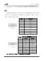
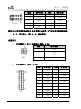
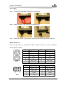
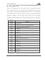
1
EC7-1813CLD2NA SERIES 基于 Intel® Luna Pier 平台 Mini-ITX 主板 Mini-ITX Motherboard Based on Intel® Luna Pier Platform Version: C02 声明 本手册包含的内容并不代表本公司的承诺,本公司保留对此手册更改的权 利,且不另行通知。对于任何因安装、使用不当而导致的直接、间接、有意或无 意的损坏及隐患概不负责。 订购产品前,请向经销商详细了解产品性能是否符合您的需求。 EVOC是研祥智能科技股份有限公司的注册商标。本手册所涉及到的其他商 标,其所有权为相应的产品厂家所拥有。 研祥智能科技股份有限公司©2010,版权所有,违者必究。未经许可,不得 以机械、电子或其它任何方式进行复制。 欲获更多信息请访问研祥网站:http://www.evoc.com 或向研祥技术支持邮箱 [email protected]、[email protected]咨询。 安全使用小常识 1. 产品使用前,务必仔细阅读产品说明书; 2. 对未准备安装的板卡,应将其保存在防静电保护袋中; 3. 在从防静电保护袋中拿出板卡前,应将手先置于接地金属物体上一会儿(比 如 10 秒钟),以释放身体及手中的静电; 4. 在拿板卡时,需佩戴静电保护手套,并且应该养成只触及其边缘部分的习 惯; 5. 为避免人体被电击或产品被损坏,在每次对主板、板卡进行拔插或重新配 置时,须先关闭交流电源或将交流电源线从电源插座中拔掉; 6. 在需对板卡或整机进行搬动前,务必先将交流电源线从电源插座中拔掉; 7. 对整机产品,需增加/减少板卡时,务必先拔掉交流电源; 8. 当您需连接或拔除任何设备前,须确定所有的电源线事先已被拔掉; 9. 为避免频繁开关机对产品造成不必要的损伤,关机后,应至少等待 30 秒后 再开机。 目录 第一章 产品介绍 ......................................................................................................1 简介 .........................................................................................................................1 机械尺寸、重量与环境..........................................................................................1 典型功耗 .................................................................................................................2 微处理器 .................................................................................................................2 芯片组 .....................................................................................................................2 系统内存 .................................................................................................................2 显示功能 .................................................................................................................2 网络功能 .................................................................................................................3 音频功能 .................................................................................................................3 电源特性 .................................................................................................................3 扩展总线 .................................................................................................................3 Watchdog功能 .........................................................................................................3 操作系统 .................................................................................................................3 I/O接口 ....................................................................................................................4 第二章 安装说明 ......................................................................................................5 产品外形尺寸图......................................................................................................5 接口位置示意图......................................................................................................6 架构图 .....................................................................................................................7 跳线设置 .................................................................................................................8 系统内存的安装......................................................................................................9 串口 .......................................................................................................................10 显示接口 ............................................................................................................... 11 LCD背光控制接口..................................................................................................13 音频接口 ...............................................................................................................13 IDE接口 .................................................................................................................14 SATA接口 ...............................................................................................................15 SATA硬盘热插拔....................................................................................................15 键盘鼠标接口........................................................................................................17 网络接口与USB接口..............................................................................................18 并口 .......................................................................................................................19 GPIO接口 ...............................................................................................................19 电源接口 ...............................................................................................................20 状态指示控制接口................................................................................................21 风扇接口 ...............................................................................................................21 CF卡 ......................................................................................................................22 扩展插槽 ...............................................................................................................23 DVI显示输出设置说明.........................................................................................24 第三章 BIOS功能介绍 ...........................................................................................27 简介 .......................................................................................................................27 BIOS参数设置 ......................................................................................................27 BIOS基本功能设置...............................................................................................28 x86 平台下BIOS所要管理的系统资源 ................................................................43 第四章 驱动程序安装说明 ....................................................................................46 附录............................................................................................................................47 Watchdog编程指引................................................................................................47 数字IO编程指引....................................................................................................49 常见故障分析与解决............................................................................................52 第一章 第一章 产品介绍 产品介绍 简介 该产品是基于 Intel® Luna Pier Refresh 平台开发的符合 Mini-ITX 单板规 范的嵌入式主板。 主板采用板载 Intel® Atom™ D510/D410 处理器 + Intel® ICH8M 的技术方 案实现。板上提供 1 个 SO-DIMM DDR2 插槽,最大内存容量可达 2GB。支持 VGA、 24 位 LVDS、DVI 三种显示;2 个 10/100/1000M 以太网控制器;8 个 USB2.0 接口; 2 个 SATA 硬盘接口;1 个 IDE 接口,1 个 Type I/II CF 接口;1 个 HD Audio 接 口;6 或 10 个 COM 口(其中 1 个支持 RS-232/ RS-485,2 个支持串口供电功能); 1 个 PS/2 键盘鼠标接口;1 个 PCI 插槽;主板采用标准 ATX 电源供电或 12V 单 电源供电。 本产品采用Intel®的低功耗解决方案,具有多串口,串口供电,支持VGA和 LVDS双显示,支持PCI扩展等特点,满足POS和彩票行业的行业需求。同时也适用 于对主板性能要求不高的广告机,查询机,自助终端等需求。 机械尺寸、重量与环境 外形尺寸:170mm(长)×177.9mm(宽)×41.5mm(高) 净重:0.436Kg; 工作环境: 温度:-10℃~60℃; 湿度:5%~95%(非凝结状态); 贮存环境: 温度:-40℃~75℃; 湿度:5%~95%(非凝结状态); EC7-1813CLD2NA SERIES - 1 - 第一章 产品介绍 典型功耗 典型功耗是基于以下配置闲置状态的数值。 1、EC7-1813CLD2NA-D4V10COM 的典型功耗如下: CPU:OnBoard Intel® Atom™ D410 1.66GHz (166*10/L2=512K) 内存:Transcend DDRII 800 2GB 硬盘:HITIACH 2TB SATA HDD [email protected];+5%/-3%; 2、EC7-1813CLD2NA-D5 的典型功耗如下: CPU:Intel® Atom™ D510 内存:DDRII800 2GB Kingston 硬盘:Seagate 500GB SATA [email protected];+5%/-3%; [email protected];+5%/-3%; [email protected];+5%/-3%。 微处理器 板载Intel® Atom™ D510(双核)/D410(单核)处理器,内部集成了内存控 制器和图形控制器。 芯片组 Intel® Atom™D510/D410处理器 + Intel® ICH8M 系统内存 提供1条200 Pin SO-DIMM DDR2内存插槽,支持Un-buffered Non-ECC内存, 支持最大内存容量2GB,支持的内存频率为667MHz。 显示功能 采用CPU内置集成图形控制器; - 2 - EC7-1813CLD2NA SERIES 第一章 产品介绍 支持VGA、单通道24位LVDS、DVI三种显示,其中24位LVDS和DVI为同源输入, LVDS和DVI输出为Clone模式;可支持VGA+LVDS(或DVI)输出,Clone或扩 展模式;可支持三显;支持热插拔功能。 VGA支持最大分辨率及刷新率为2048×1536@60Hz;LVDS支持的最大分辨率 为1366×768;DVI支持的最大分辨率为1600X1200。 网络功能 提供2个10/100/1000Mbps网络接口,LAN1可支持网络唤醒功能;LAN1可支持 网络PXE启动。 音频功能 采用HD标准,支持 MIC-IN/LINE-IN/LINE-OUT。 电源特性 采用ATX/AT电源,ATX电源支持 ACPI1.0b 规范,支持S0、S1、S4、S5状态, AT电源支持单12V电源供电。 扩展总线 提供1个PCI插槽,兼容PCI 2.3标准。 Watchdog功能 支持 255 级,可编程按分或秒; 支持看门狗超时中断或复位系统。 操作系统 支持操作系统:Windows XP、Windows 2000、Linux。 EC7-1813CLD2NA SERIES - 3 - 第一章 产品介绍 I/O接口 提供 1 个并口,支持 SSP/EEP/ECP 工作模式;支持 BIOS 修改工作模式; 提供 10 个串口,其中 COM2 支持 RS-232/RS-485 模式选择;COM1 支持 Modem 唤醒功能;COM3,COM4 支持 5V/12V 电源输出; 提供 1 个 IDE 接口; 提供 1 个 CF 卡接口; 提供 2 个 SATA 接口,支持热插拔功能; 提供 8 个 USB2.0 接口;USB1~USB4 直接由连接器形式接出,USB5~USB8 采用 2×5Pin 插针引出; 提供 2 个 PS/2 键盘/鼠标接口,其中 1 个为标准接口,1 个为插针接口; 提供 1 个 8 路数字 I/O 接口。 提示:如何识别报警声 1、长鸣声为系统内存出错。 2、短“嘀”一声为开机声。 - 4 - EC7-1813CLD2NA SERIES 第二章 安装说明 第二章 安装说明 产品外形尺寸图 H1 33 H4 170 154.9 132.1 H2 H3 4.9 157.5 170 6.4 单位:mm 警告! 请务必选择合适的螺钉和使用正确的安装方法(包括板卡定位、CPU、散热 器等安装),否则可能损坏板。此板推荐 H1~H4 使用 M3×6 GB9074.4-88 螺钉。 EC7-1813CLD2NA SERIES - 5 - 第二章 安装说明 接口位置示意图 H1 AUDIO1 J1 J2 J4 AUDIO2 J3 KM1 COM9 COM7 COM5 COM3 COM10 COM8 COM6 COM4 JP3 JP4 PCI1 JCC1 H4 JP5 JP6 JP2 JLCD1 J5 LCDB1 LVDS1 LPT1 GPIO1 J6 KM2 SYSFAN1 CPUFAN1 PWR3 U1 SATA2 PWR2 JCF1 SATA1 JP1 IDE1 PWR1 CF1 H2 FP1 FP2 FP3 DIMM1 - 6 - H3 EC7-1813CLD2NA SERIES 第二章 安装说明 架构图 VGA DB15 D510(DC)/ D410(SC)CPU DVI CH A DDR2 SODIMM1 DDR2 Terminaltion CH7036 LVDS 24BIT DMI SATA SATA II X2(1*7) USB 2.0 X4 (标准 ) USB 2.0 X4 (插针 ) USB PCI-E Port1 RTL8111D LAN1 RJ45 Connector PCI-E Port 2 82574L LAN2 RJ45 Connector ICH8M 82801HM IDE1(44pin) PATA HDA ALC888 SPI SPI Flash SM Bus 9534 CF1(TYPE II) PCI 槽 PCI 内接插针 标准接口 8路GPIO LPC BUS F81216D IT8782 Hardware Monitor Parallel 插针 PS/2键鼠 外接或内接 WDT COM1 (RS232) COM2 (RS232/485) COM3/4(RS232)插针 第 9PIN可选 RI/5V/12V COM7/8/9/10 ( RS232插针) COM5/6 (RS232)插针 提示:如何识别跳线、接口第一脚 1、观察插头、插座旁边的文字标记,通常用“1”或加粗的线条或三角符号表示。 2、看看背面的焊盘,通常方型焊盘为第一脚。 EC7-1813CLD2NA SERIES - 7 - 第二章 安装说明 跳线设置 1. JCC1:CMOS内容清除/保持设置(脚距:2.0mm) CMOS由板上钮扣电池供电。清CMOS会导致永久性消除以前系统配置并将其设 为原始(工厂设置)系统设置。其步骤:(1)关闭计算机,断开电源;(2)瞬间短 接JCC1插针;(3)开计算机;(4)启动时按屏幕提示按键进入BIOS设置,重新加载 最优缺省值;(5)保存并退出设置。设置方式如下: JCC1 2. 设置 功能 1-2 开路 正常工作状态(Default) 1-2 短路 清除 CMOS 内容,所有 BIOS 设置恢复成出厂值。 JLCD1:LCD工作电压选择(脚距:2.0mm) 不同的LCD屏电压可能不同,本板提供了3.3V和5V两种电压选择,当所选择 的LCD电压与所使用的LCD屏的工作电压一致时,LCD屏才能正常显示。设置方式 如下: JLCD1 3. 设置 功能 1-2 短路 +3.3V(Default) 2-3 短路 +5V JCF1:CF卡工作电压选择(脚距:2.0mm) 不同的CF卡的工作电压可能不同,本板提供了3.3V和5V两种电压选择,当所 选择的CF卡工作电压与所使用的CF卡工作电压一致时,才能保证系统的稳定性。 设置方式如下: JCF1 设置 功能 1-2 短路 +3.3V 2-3 短路 +5V(Default) 注:CF卡电压选择是为兼容不同的CF卡而设置,对未明确标示工作电压的CF卡 需根据实际使用情况选择CF卡电压。 - 8 - EC7-1813CLD2NA SERIES 第二章 4. 安装说明 JP1:CF卡主从模式选择 (脚距:2.0mm) JP1 5. 设置 功能 1-2 短路 Master 1-2 开路 Slave(Default) JP2~JP4:COM2串口模式选择(脚距:2.0mm) 模式选择 管脚 设置 JP2 JP3~JP4 6. RS-232 RS-485 (Default) JP2 1-2 3-4 JP3 1-2 2-3 JP4 1-2 2-3 JP5~JP6:COM3/COM4串口 Pin 9功能选择(脚距:2.0mm) COM3/COM4 Pin9 功能选择 管脚 JP5/JP6 设置 RI#(Default) VCC5V VCC12V JP5 1-2 3-4 5-6 JP6 1-2 3-4 5-6 系统内存的安装 本板提供 1 条 200Pin DDRⅡ SO-DIMM 插槽(DIMM1)。安装内存条时,要注 意以下几点: 拨开内存槽两边的耳扣,安装时先将内存条的缺口和内存槽的缺口对准后 再向下用力压到位。 使用符合该主板 Intel® Chipset 所支持的 1.8V DDRⅡ 667MHz 规格的内 存,主板支持最大内存容量达 2GB。 EC7-1813CLD2NA SERIES - 9 - 第二章 安装说明 最好选择带 SPD(内存自动识别功能)的内存条,以保证内存条工作稳定。 串口 本板提供2个标准DB9串口,其中COM1支持Modem唤醒功能和RS-232模式,COM2 支持RS-232/RS-485模式选择;另外提供8个2×5Pin插针串口(脚距:2.54mm), 支持RS-232模式,管脚定义如下: 管脚 信号名称 1 DCD# 2 RXD 3 TXD 4 DTR# 5 GND 6 DSR# 7 RTS# 8 CTS# 9 RI# J1(COM1) 管脚 J1(COM2) 信号名称 RS-232 RS-485 1 DCD# Data- 2 RXD Data+ 3 TXD NC 4 DTR# NC 5 GND GND 6 DSR# NC 7 RTS# NC 8 CTS# NC 9 RI# NC 注:COM2 在 RS-485 模式下,数据收发方向为自动控制。 - 10 - EC7-1813CLD2NA SERIES 第二章 安装说明 COM3~COM10 管脚 信号名称 1 DCD# 2 RXD 3 TXD 4 DTR# 5 GND 6 DSR# 7 RTS# 8 CTS# 9 RI# 10 NA 显示接口 本板提供一组24位单通道LVDS接口和1个VGA+DVI-D的双层接口(板上标识为 J2:下层为DVI接口,上层为VGA接口)。管脚定义如下: 1. VGA接口 J2(VGA) 管脚 信号名称 管脚 信号名称 1 Red 2 Green 3 Blue 4 NC 5 GND 6 GND 7 GND 8 GND 9 NC 10 GND 11 NC 12 DDCDATA 13 HSYNC 14 VSYNC 15 DDCCLK EC7-1813CLD2NA SERIES - 11 - 第二章 2. DVI-D 接口 J2(DVI) 3. 安装说明 管脚 信号名称 管脚 信号名称 1 DATA2- 13 NC 2 DATA2+ 14 +5V 3 GND_DVI 15 GND 4 NC 16 HOTPLUG 5 NC 17 DATA0- 6 DDCCLK 18 DATA0+ 7 DDCDATA 19 GND_DVI 8 NC 20 NC 9 DATA1- 21 NC 10 DATA1+ 22 GND_DVI 11 GND_DVI 23 CLK+ 12 NC 24 CLK- 单通道24位LVDS接口 LVDS1 (脚距:1.0mm) 管脚 信号名称 管脚 信号名称 1 LVDS_D0+ 2 LVDS_D0- 3 GND 4 GND 5 LVDS_D1+ 6 LVDS_D1- 7 GND 8 GND 9 LVDS_D2+ 10 LVDS_D2- 11 GND 12 GND 13 CLK+ 14 CLK- 15 GND 16 GND 17 LVDS_D3+ 18 LVDS_D3- 19 VDD 20 VDD 注:本主板用到LVDS插座型号为DF20G-20DP-1V;对应端子的型号为DF20A-20DF-1C。 - 12 - EC7-1813CLD2NA SERIES 第二章 安装说明 LCD背光控制接口 本板提供1个1×4Pin LCD背光控制接口(脚距:2.0mm),管脚定义如下: LCDB1 管脚 信号名称 1 VCC_LCDBKLT 2 LCD_BKLTCTL 3 LCD_BKLTEN 4 GND 注:VCC_LCDBKLT---+12V背光电源(此脚电流限制在1A以下); LCD_BKLTCTL---背光控制(该信号由Pineview D输出,为PWM信号,电压幅 值0V~3.3V,占空比在0~100%之间); LCD_BKLTEN ----背光使能,高有效。 音频接口 本板提供1个双层Audio接口和1个2×5Pin AUDIO插针接口。 AUDIO1 AUDIO2 (脚距:2.0mm) 管脚 信号名称 1 LINE_OUT 2 MIC_IN 管脚 信号名称 管脚 信号名称 1 LOUT_R 2 LOUT_L 3 GND_AUDIO 4 GND_AUDIO 5 LIN_R 6 LIN_L 7 GND_AUDIO 8 GND_AUDIO 9 MIC_L 10 MIC_R EC7-1813CLD2NA SERIES - 13 - 第二章 安装说明 IDE接口 本板提供一组并行IDE接口(脚距:2.0mm),并与CF卡接口共用IDE总线, 故安装IDE设备时,需注意以下: 如果 CF 卡接口插有 CF 存储卡,IDE 接口只可以连接一台 IDE 设备,并且 CF 存储卡与 IDE 设备,一个为主设备(Master),一个为从设备(Slave), CF 存储卡主从可通过 JP1 来设备,硬盘上提供相应的跳线来将其配置成主 设备还是从设备使用; 如果 CF 卡接口没有使用 CF 存储卡,IDE 接口可以连接两台 IDE 设备,设备 的连接方法是:主设备接在电缆的末端,从设备接在电缆的中间;连接使 用 Ultra 66/100 的硬盘时,必须使用 80 线的专用扁平电缆。 IDE1 - 14 - 管脚 信号名称 1 RESET# 管脚 2 3 D7 4 D8 5 D6 6 D9 7 D5 8 D10 9 D4 10 D11 11 D3 12 D12 13 D2 14 D13 15 D1 16 D14 17 D0 18 D15 19 GND 20 Key 21 DREQ 22 GND 23 IOW# 24 GND 25 IOR# 26 GND 27 IORDY 28 GND EC7-1813CLD2NA SERIES 信号名称 GND 第二章 安装说明 29 DACK# 30 GND 31 IRQ 32 NC 33 DA1 34 ATA66_DET 35 DA0 36 DA2 37 CS1# 38 CS3# 39 LED# 40 GND 41 +5V 42 +5V GND 44 GND 43 SATA接口 提供2个SATA插座,管脚定义如下: 管脚 SATA1/SATA2 信号名称 1 GND 2 TX+ 3 TX- 4 GND 5 RX- 6 RX+ 7 GND SATA硬盘热插拔 SATA 硬盘热插拔需注意: (1) 硬盘必须支持:SATA 2.0 接口,并且采用 15 芯 SATA 硬盘电源接口。 (2) 芯片组驱动程序支持 SATA 硬盘的热插拔。 (3) 不能对操作系统所在的 SATA 硬盘进行带电热插拔。 SATA 硬盘数据线 EC7-1813CLD2NA SERIES SATA 硬盘电源线 - 15 - 第二章 安装说明 请按照如下步骤进行 SATA 硬盘热插拔,否则,操作不当会导致硬盘损坏和 数据丢失。 热插入SATA硬盘步骤: 步骤1:请将SATA电源线1x4-针脚(白色)一端接到电源适配器的1x4-针脚电 源线一端。 步骤2:将SATA 数据线接到主板上的SATA接口。 步骤3:将SATA电源线15-针脚接口(黑色)一端接到SATA硬盘。 步骤4:将SATA数据线接到SATA硬盘。 - 16 - EC7-1813CLD2NA SERIES 第二章 安装说明 热拔出SATA硬盘步骤: 步骤 1:从设备管理器中卸载该硬盘。 步骤 2:从 SATA 硬盘一侧拔去 SATA 数据线。 步骤 3:从 SATA 硬盘一侧拔去 SATA 15-针脚电源线接口(黑色)。 键盘鼠标接口 此板提供1个标准的PS/2键盘/鼠标组合接口和1个插针键盘鼠标接口(脚距: 2.0mm)。 管脚 信号名称 管脚 信号名称 1 KB_DATA 7 MS_DATA 2 NC 8 NC 3 GND 9 GND 4 +5V 10 +5V 5 KB_CLK 11 MS_CLK 6 NC 12 NC KM1 KM2 管脚 信号名称 管脚 信号名称 1 KB_DATA 2 MS_DATA 3 KB_CLK 4 MS_CLK 5 GND 6 GND 7 +5V 8 +5V EC7-1813CLD2NA SERIES - 17 - 第二章 安装说明 网络接口与USB接口 主板上共提供2个网络接口与及8个USB接口,其中每个网络接口与2个USB共 用一组模(即J3、J4分别包括1个网口和2个USB接口)。此外主板还提供2个2X5 Pin 插针形式的USB接口(J5,J6),可以连接4个USB。 网络接口 主板上有2个10/100/1000Mbps以太网接口,LILED和ACTLED是以太网接口两 边的LED指示灯,它们显示着LAN的活动和传输状态。请参考以下每一个LED的状 态描述: J3(LAN1),J4(LAN2) LILED 网络速度 (双色:橙绿双色) 指示状态 绿色 1000Mbps 有数据传输 橙色 100Mbps 无数据传输 灭 10Mbps ACTLED 网络活动 (单色:绿色灯) 指示状态 闪烁 灭 USB接口 J3(USB1/USB2) J4(USB3/USB4) - 18 - 管脚 信号名称 1 +5V 2 USB_Data- 3 USB_Data+ 4 GND EC7-1813CLD2NA SERIES 第二章 安装说明 J5(USB5/USB6) J6(USB7/USB8) 脚距:2.54mm 管脚 信号名称 管脚 信号名称 1 +5V 2 +5V 3 USB1_Data- 4 USB2_Data- 5 USB1_Data+ 6 USB2_Data+ 7 GND 8 GND 9 NA 10 GND 并口 本板提供1个2×13Pin插针并口(脚距:2.0mm)。 LPT1 管脚 信号名称 管脚 信号名称 1 STB# 2 AFD# 3 PD0 4 ERR# 5 PD1 6 INIT# 7 PD2 8 SLIN# 9 PD3 10 GND 11 PD4 12 GND 13 PD5 14 GND 15 PD6 16 GND 17 PD7 18 GND 19 ACK# 20 GND 21 BUSY 22 GND 23 PE 24 GND 25 SLCT 26 NC GPIO接口 本板提供1个2×5Pin GPIO插针接口(脚距:2.0mm)。 EC7-1813CLD2NA SERIES - 19 - 第二章 GPIO1 安装说明 管脚 信号名称 管脚 信号名称 1 GPIO1 2 GPIO5 3 GPIO2 4 GPIO6 5 GPIO3 6 GPIO7 7 GPIO4 8 GPIO8 9 GND 10 NC 说明:GPIO各引脚是双向信号,为方便测试与应用,出厂默认值为连接器的第1, 3,5,7脚为输入,第2,4,6,8脚为输出。 电源接口 1) AT电源接口:单12V 电源接口(脚距:4.2mm) PWR2 2) 信号名称 1 GND 2 GND 3 +12V 4 +12V ATX电源接口(脚距:4.2mm) PWR1 - 20 - 管脚 管脚 信号名称 管脚 信号名称 1 +3.3V 11 +3.3V 2 +3.3V 12 -12V 3 GND 13 GND 4 +5V 14 PS_ON# 5 GND 15 GND 6 +5V 16 GND 7 GND 17 GND 8 PWROK 18 -5V 9 +5VSB 19 +5V 10 +12V 20 +5V EC7-1813CLD2NA SERIES 第二章 安装说明 3) SATA电源转接接口(脚距:5.08mm) 管脚 信号名称 1 +12V 2 GND 3 GND 4 +5V PWR3 状态指示控制接口 1) ATX电源开关及硬盘指示灯接口(脚距:2.54mm) FP1 2) 管脚 信号名称 管脚 信号名称 1 PWRBTN# 2 GND 3 GND 4 RESET# 5 HDD_LED- 6 HDD_LED+ 电源指示灯接口(脚距:2.54mm) 管脚 信号名称 1 PWR_LED+ 2 NC 3 GND FP2 3) 扬声器输出接口(脚距:2.54mm) FP3 管脚 信号名称 1 SPEAKER 2 NC 3 4 GND +5V 风扇接口 本板提供2个1×3Pin风扇接口(脚距:2.54mm)。 CPUFAN1,SYSFAN1 管脚 信号名称 1 GND 2 +12V 3 FAN_IO FAN_IO :风扇转速脉冲输出。 EC7-1813CLD2NA SERIES - 21 - 第二章 安装说明 CF卡 板上标识为CF1。 管脚 信号名称 管脚 信号名称 1 GND 26 CD1# 2 D3 27 D11 3 D4 28 D12 4 D5 29 D13 5 D6 30 D14 6 D7 31 D15 7 CS0# 32 CS1# 8 GND 33 VS1# 9 ATASEL# 34 IOR# 10 GND 35 IOW# 11 GND 36 WE# 12 GND 37 IRQ 13 VCC 38 VCC 14 GND 39 CSEL# 15 GND 40 VS2# 16 GND 41 RESET# 17 GND 42 IORDY 18 A2 43 DREQ 19 A1 44 DACK# 20 A0 45 DASP# 21 D0 46 ATA66_DET 22 D1 47 D8 23 D2 48 D9 24 WP/IOCS16# 49 D10 25 CD2# 50 GND - 22 - EC7-1813CLD2NA SERIES 第二章 安装说明 扩展插槽 PCI插槽作为标准PCI(version 2.3)接口(PCI1),管脚定义如下: 管脚 信号名称 管脚 信号名称 管脚 信号名称 管脚 信号名称 A1 TRST# A31 PCI_AD18 B1 -12V B31 +3.3V A2 +12V A32 PCI_AD16 B2 TCK B32 PCI_AD17 A3 TMS A33 +3.3V B3 GND B33 PCI_C/BE#2 A4 TDI A34 PCI_FRAME# B4 TDO B34 GND A5 +5V A35 GND B5 +5V B35 PCI_IRDY# A6 INTA# A36 PCI_TRDY# B6 +5V B36 +3.3V A7 INTC# A37 GND B7 INTB# B37 PCI_DEVSEL# A8 +5V A38 PCI_STOP# B8 INTD# B38 GND A9 Null A39 +3.3V B9 PRSNT1# B39 PCI_PLOCK# A10 +5V A40 SMCLK B10 Null B40 PCI_PERR# A11 Null A41 SMDATA B11 PRSNT2# B41 +3.3V A12 GND A42 GND B12 GND B42 PCI_SERR# A13 GND A43 PCI_PAR B13 GND B43 +3.3V A14 3.3Vaux A44 PCI_AD15 B14 Null B44 PCI_C/BE#1 A15 PCI_RST# A45 +3.3V B15 GND B45 PCI_AD14 A16 +5V A46 PCI_AD13 B16 PCI_CLK B46 GND A17 PCI_GNT# A47 PCI_AD11 B17 GND B47 PCI_AD12 A18 GND A48 GND B18 PCI_REQ# B48 PCI_AD10 A19 PCI_PME# A49 PCI_AD9 B19 +5V B49 GND A20 PCI_AD30 A50 PCI_C/BE#0 B20 PCI_AD31 B50 PCI_AD8 A21 +3.3V A51 +3.3V B21 PCI_AD29 B51 PCI_AD7 A22 PCI_AD28 A52 PCI_AD6 B22 GND B52 +3.3V A23 PCI_AD26 A53 PCI_AD4 B23 PCI_AD27 B53 PCI_AD5 A24 GND A54 GND B24 PCI_AD25 B54 PCI_AD3 A25 PCI_AD24 A55 PCI_AD2 B25 +3.3V B55 GND A26 PCI_IDSEL A56 PCI_AD0 B26 PCI_C/BE#3 B56 PCI_AD1 A27 +3.3V A57 +5V B27 PCI_AD23 B57 +5V A28 PCI_AD22 A58 PCI_REQ64# B28 GND B58 PCI_ACK64# A29 PCI_AD20 A59 +5V B29 PCI_AD21 B59 +5V A30 GND A60 +5V B30 PCI_AD19 B60 +5V 注:若使用PWR2供电时,管脚B1为NC。 EC7-1813CLD2NA SERIES - 23 - 第二章 安装说明 DVI显示输出设置说明 本产品支持VGA、LVDS、DVI三种显示;DVI显示和LVDS显示是Clone模式,设 置如下: 1. 进入 BIOS 菜单,设置带有 DVI 显示模式,如下图: 2. 第一次安装操作系统完成之后,需要安装 DVI 的驱动程式,按出货光盘配 置安装,此驱动只设置 DVI 显示功能。客户根据自己所接 LVDS 屏选择 18 位/24 位 LVDS 输出,详细设置部分见驱动程序中的 Readme.txt 部分。安装完成驱动后 图示如下: - 24 - EC7-1813CLD2NA SERIES 第二章 3. 安装说明 设置 DVI 分辨率,主板在读取显示器支持的分辨率之后,会显示出显示器 本身可支持的分辨率,如下图: EC7-1813CLD2NA SERIES - 25 - 第二章 4. 设置 DVI 显示尺寸,DVI 显示可以拉伸屏幕尺寸,如下图: 5. 驱动设置后,有记忆功能,下次开机显示后仍按此次参数配置。 安装说明 6. DVI 显示功能是由 CH7036A 方案实现,方案本身需遵循以下建议:建议一, DVI 选择输出的分辨率不小于 BIOS 菜单下选择的 LVDS 分辨率,若 DVI 输出的分 辨率低于 LVDS 分辨率,可能会出现某些分辨率下字体模糊问题。建议二,若背 景选为纯浅蓝色,在某些分辨率下会出现轻微的竖条纹,这是由于 CH7036A 方案 的实现机制所形成的,属正常现象。 - 26 - EC7-1813CLD2NA SERIES 第三章 第三章 BIOS 功能介绍 BIOS功能介绍 简介 BIOS(Basic Input and Output System:基本输入输出系统)固化在 CPU 板上的闪存存储器中,主要功能包括:初始化系统硬件,设置各系统部件的工作 状态,调整各系统部件的工作参数,诊断系统各部件的功能并报告故障,给上层 软件系统提供硬件操作控制接口,引导操作系统等。BIOS 提供用户一个菜单式 的人机接口,方便用户配置各系统参数设置,控制电源管理模式,调整系统设备 的资源分配等等。 正确设置 BIOS 各项参数,可使系统稳定可靠地工作,同时也能提升系统的 整体性能。不适当的甚至错误的 BIOS 参数设置,则会使系统工作性能大为降低, 使系统工作不稳定,甚至无法正常工作。 BIOS参数设置 每当系统接通电源,正常开机后,便可看见进入 BIOS 设置程序提示的信息。 此时(其它时间无效),按下提示信息所指定的按键(通常为<Del>键)即可进入 BIOS 设置程序。 CMOS 中 BIOS 设置内容被破坏时,系统也会要求进入 BIOS 设置或选择某种 默认设置值。 通过BIOS修改的所有设置值都保存在系统的CMOS存储器中,该CMOS存储器 由电池供电,即使切断外部电源,其内容也不会丢失,除非执行清除CMOS内容的 操作。 注意!BIOS的设置直接影响到电脑的性能,设置错误的参数将造成电脑的 损坏,甚至不能开机,请清CMOS后再使用BIOS内置缺省值来恢复系统正常运行。 由于本公司不断研发更新BIOS,其设置界面也会略有不同,以下的画面供 您参考,有可能跟您目前所使用的BIOS设置程序不完全相同。 EC7-1813CLD2NA SERIES - 27 - 第三章 BIOS 功能介绍 BIOS基本功能设置 当SETUP程序启动之后,您可以看到CMOS Setup Utility主画面如下: BIOS SETUP UTILITY System Overview Processor Type : Intel(R) Atom(TM) CPU K510 Speed Cores @ 1.66GHz :1666MHz :2 ←→ ↑↓ + Tab F1 F10 ESC Select Screen Select Item Change Field Select Field General Help Save and Exit Exit System Memory Size :1015MB System Time System Date [00:47:55] [Mon 01/11/2010] V02.57 (c)Copyright 1985-2004,American Megatrends, Inc. Main System Time 选择此选项,用< + > / < - >来设置目前的时间。以时/分/秒的格式来表 示。各项目合理的范围是:Hour/时(00-23), Minute/分(00-59),Second/秒 (00-59)。 System Date 选择此选项,用< + > / < - >来设置目前的日期。以月/日/年的格式来表 示。各项目合理的范围是:Month/月(Jan.-Dec.), Date/日(01-31),Year/年(最 大至 2099), Week/星期(Mon.~ Sun.)。 - 28 - EC7-1813CLD2NA SERIES 第三章 BIOS 功能介绍 Advanced BIOS SETUP UTILITY Configure CPU Advanced Settings WARNING:Setting wrong values in below sections may cause system to malfunction CPU Configuration IDE Configuration Super I/O Configuration Hardware Health Configuration USB Configuration Power Management Configuration Clock Generator Configuration ←→ Select Screen ↑↓ Select Item Enter Go to Sub Screen Tab Select Field F1 General Help F10 Save and Exit ESC Exit V02.57 (c)Copyright 1985-2004, American Megatrends, Inc. CPU Configuration BIOS SETUP UTILITY Configure advanced CPU settings Brand String: Intel(R) Atom(TM) CPU K510 @ 1.66GHz Frequency; :1.66GHz FSB Speed; :667MHz Cache L1; :48 KB Cache L2; :1024 KB Ratio Actual Value :10 Hyper Threading Technology [Enabled] Intel(R) SpeedStep(tm) tech [Enabled] ←→ ↑↓ + Tab F1 F10 ESC Select Screen Select Item Change Field Select Field General Help Save and Exit Exit V02.57 (c)Copyright 1985-2004, American Megatrends, Inc EC7-1813CLD2NA SERIES - 29 - 第三章 BIOS 功能介绍 Hyper Threading Technology Intel Hyper Threading Technology功能的控制开关。 Intel(R) SpeedStep(tm) tech Intel(R) SpeedStep(tm) tech功能的控制开关。 IDE Configuration BIOS SETUP UTILITY IDE Configuration ATA/IDE Configuration Configure SATA as [Enhanced] [IDE] Primary IDE Master :[Not Detected] Primary IDE Slave :[Not Detected] Secondary IDE Master :[Not Detected] Secondary IDE Slave :[Not Detected] Third IDE Master :[Not Detected] Third IDE Slave :[Not Detected] ←→ ↑↓ + Tab F1 F10 ESC Select Screen Select Item Change Field Select Field General Help Save and Exit Exit V02.57 (c)Copyright 1985-2004, American Megatrends, Inc. ATA/IDE Configuration 此选项用来配置ATA的工作模式,Enhanced和Compatible分别对应增强模式 和兼容模式。 Configure SATA as SATA 控 制 器 的 类 型 选 择 , 对 应 IDE 和 AHCI 选 择 项 , 仅 在 ATA/IDE Configuration为增强模式时才支持AHCI。 AHCI功能同时需要硬件芯片和操作系统支持。 - 30 - EC7-1813CLD2NA SERIES 第三章 BIOS 功能介绍 Legacy IDE Channels 配置兼容模式下IDE通道类型,对应SATA Only,SATA Pri,PATA Sec和PATA Only选择项。 Primary~Third IDE Master/Slave ﹡Type Not Installed:系统没有检测到IDE设备 AUTO:系统开机自动检测IDE参数 CD/DVD:用于ATAPI CDROM ARMD:用于各种模拟IDE设备 ﹡LBA/Large Mode 用于设置是否支持LBA模式。 ﹡Block(Multi-sector Transfer) 用于设置是否支持多扇区同时传输的功能。 ﹡PIO Mode 用于PIO模式设置。 ﹡DMA Mode 用于DMA模式设置。 ﹡S.M.A.R.T 此选项用于设置是否启用硬盘S.M.A.R.T功能,只对支持该功能的硬盘有 效。 ﹡32Bit Data Transfer 此选项用于使能32位的硬盘访问模式,可以使硬盘读写速度达到最佳。 AHCI Port0~2 AHCI 端口配置菜单,仅在SATA控制器配置成AHCI或RAID时显示。 ﹡SATA Port0~2 Auto:系统开机自动检测SATA设备。 Not Installed:关闭该端口,不做检测。 ﹡S.M.A.R.T 此选项用于设置是否启用硬盘S.M.A.R.T功能,只对支持该功能的硬盘有 效。 EC7-1813CLD2NA SERIES - 31 - 第三章 BIOS 功能介绍 Super I/O Configuration BIOS SETUP UTILITY Configure Super I/O Chipset OnBoard Floppy Controller [Enabled] Serial Port1 Address [3F8] Serial Port1 IRQ [4] Serial Port2 Address [2F8] Serial Port2 IRQ [4] Serial Port3 Address [3E8] Serial Port3 IRQ [3] Serial Port4 Address [2E8] Serial Port4 IRQ [3] Serial Port5 Address [2F0] Serial Port5 IRQ [10] Serial Port6 Address [2E0] Serial Port6 IRQ [10] Serial Port7 Address [200] Serial Port7 IRQ [11] Serial Port8 Address [208] Serial Port8 IRQ [11] Serial Port9 Address [210] Serial Port9 IRQ [11] Serial Port10 Address [218] Serial Port10 IRQ [11] Parallel Port Address [378] Parallel Port Mode [Normal] Parallel Port IRQ [IRQ7] Uart IRQ Attribute Allows BIOS to Enable or Disable Floppy Controller. ←→ ↑↓ + Tab F1 F10 ESC Select Screen Select Item Change Field Select Field General Help Save and Exit Exit [Edge Active High] V02.57 (c)Copyright 1985-2004, American Megatrends, Inc. - 32 - EC7-1813CLD2NA SERIES 第三章 BIOS 功能介绍 OnBoard Floppy Controller 用于使能软驱控制器。 Serial Port n Address 设定主机板上串口n的地址(n=1…10)。 Serial Port n IRQ 设定主机板上串口n的中断(n=1…10)。 Parallel Port Address 设定主机板上并口的地址,地址缺省值为378。 Parallel Port Mode 设定主机板上并口的模式。 Parallel Port IRQ 设定主机板上并口的中断。 Uart IRQ Attribute 设定串口7-10的中断属性。 EC7-1813CLD2NA SERIES - 33 - 第三章 BIOS 功能介绍 Hardware Health Configuration BIOS SETUP UTILITY Hardware Health Configuration System Temperature : 30℃/86℉ CPU Temperature Enables Hardware Health Monitoring Device : 37℃/98℉ SYSFAN1 CPUFAN1 Vcore : 1.136 V V3.3 : 3.296 V V5.0 : 5.094 V V12.0 : 12.196 V VBAT : 3.152 V ←→ ↑↓ + Tab F1 F10 ESC Select Screen Select Item Change Field Select Field General Help Save and Exit Exit V02.57 (c)Copyright 1985-2004, American Megatrends, Inc. System Temperature 当前系统温度,一般主板上有热敏电阻监测。 CPU Temperature 当前CPU温度。CPU的温度由板上的温度传感器监测。 Vcore CPU核心电压。 V3.3/ V5.0/ V12.0 开关电源输出电压。 VBAT 电池电压监测 - 34 - EC7-1813CLD2NA SERIES 第三章 BIOS 功能介绍 USB Configuration BIOS SETUP UTILITY Enables USB host controllers. USB Configuration USB Devices Enabled : 1 Keyboard, 1 Drive USB Function USB 2.0 Controller [8 USB Ports] [Enabled] Legacy USB Support [Auto] USB Mass Storage Device Configuration ←→ ↑↓ + F1 F10 ESC Select Screen Select Item Change Field General Help Save and Exit Exit V02.57 (c)Copyright 1985-2004, American Megatrends, Inc. USB Function 此选项设置USB控制器的数量,即确定支持几个USB控制器,通常一个控制 器有两个USB接口。 USB 2.0 Controller 此选项用来选择是否支持USB 2.0 控制器。 Legacy USB Support 此选项用于支持传统的USB设备(键盘,鼠标,存储设备等),当该项设为 Enabled时,即使不支持USB的操作系统如DOS下也能使用USB设备。 USB Mass Storage Device Configuration 此选项用于配置USB块存储设备,其中包括Reset 延时设置及枚举类型。 EC7-1813CLD2NA SERIES - 35 - 第三章 BIOS 功能介绍 Power Management Configuration BIOS SETUP UTILITY Power Management Configuration ACPI APIC Support [Enabled] Restore on AC Power Loss [Last state] Resume on RTC Alarm [Disabled] ←→ ↑↓ + F1 F10 ESC Select Screen Select Item Change Field General Help Save and Exit Exit V02.57 (c)Copyright 1985-2004, American Megatrends, Inc. ACPI APIC Support 此选项用于打开或关闭ACPI OS下的APIC(高级中断控制器)。 Restore on AC Power Loss 使用该选项可以设置计算机在交流电停电而后再来电时系统所处状态。 “Power Off”,让系统处于关机状态,“Power On”,系统自动开启,“Last State”,则保持到断电前的状态。 Resume on RTC Alarm 此项用来打开或关闭系统闹钟,当到达指定时间时,会将系统从节电模式 甚至关机状态唤醒,该功能必须有ATX电源的支持。 - 36 - EC7-1813CLD2NA SERIES 第三章 BIOS 功能介绍 Clock Generator Configuration BIOS SETUP UTILITY Configure Clock Generator Spread Spectrum [Enabled] Auto PCI Clock [Enabled] ←→ ↑↓ + F1 F10 ESC Select Screen Select Item Change Field General Help Save and Exit Exit V02.57 (c)Copyright 1985-2004, American Megatrends, Inc. Spread Spectrum 此选项用来控制时钟信号的展频功能。 Auto PCI Clock 此选项用来实现PCI槽上设备的自动侦测,如果槽上无设备,则关闭该槽对 应的时钟信号。 EC7-1813CLD2NA SERIES - 37 - 第三章 BIOS 功能介绍 Chipset BIOS SETUP UTILITY Advanced Chipset Settings WARNING: Setting wrong values in below sections may cause system to malfunction. North Bridge Chipset Configuration DRAM Frequency [Auto] ←→ Select Screen Initiate Graphic Adapter [PCI/IGD] ↑↓ Select Item Boot Display Device [CRT+LVDS] Enter Go to Sub LVDS Color Depth [24BIT] Screen General Help Flat Panel Type [800x600/S/18/G104S] F1 F10 Save and Exit UserDefine Panel Type [Disabled] ESC Exit South Bridge Chipset Configuration Configure DRAM Timing by SPD [Enabled] PXE Boot [Disabled] Onboard Audio Controller [Enabled] V02.57 (c)Copyright 1985-2004, American Megatrends, Inc. DRAM Frequency 配置DRAM的频率,此处建议使用自动,手动更改配置可能会因为DRAM不支 持而不开机。 Configure DRAM Timing by SPD BIOS按照SPD芯片上的内容配置SDRAM内存的时序。绝大多数内存条上有一 个保存内存时序和容量等参数的一个小芯片,即SPD芯片。 Initiate Graphic Adapter 此选项用于指定优先启动的显示设备类型。 Boot Display Device 此选项用于选择开机默认的显示输出设备。 - 38 - EC7-1813CLD2NA SERIES 第三章 BIOS 功能介绍 LVDS Color Depth 此选项用于选择LVDS的色深。 Flat Panel Type 此选项用于选择Flat Panel的分辨率。 UserDefine Panel Type 可以根据用户自定义配置平板显示类型。 PXE Boot 此选项用于选择是否打开网络启动功能。 Onboard Audio Controller 选择是否打开声卡控制器。 PCIPnP BIOS SETUP UTILITY Advanced PCI/PnP Settings WARNING:Setting wrong values in below sections may cause system to malfunction. IRQ3 [Available] IRQ4 [Available] IRQ5 [Available] IRQ7 [Available] IRQ9 [Available] IRQ10 [Available] IRQ11 [Available] IRQ14 [Available] IRQ15 [Available] ←→ ↑↓ + F1 F10 ESC Select Screen Select Item Change Field General Help Save and Exit Exit V02.57 (c)Copyright 1985-2004, American Megatrends, Inc. IRQ3~15 此系列选项用以指定对应IRQ号是PNP方式还是保留给ISA使用。 EC7-1813CLD2NA SERIES - 39 - 第三章 BIOS 功能介绍 Boot BIOS SETUP UTILITY Boot Settings Quick Boot [Enabled] Quiet Boot [Disabled] Waite For ‘F1’ If Error [Enabled] Boot Device Priority Boot from Embedded WinCE [No] 1st Boot Device [USB:aigo USB DISK] ←→ Select Screen ↑↓ Select Item Enter Go to Sub Screen F1 General Help F10 Save and Exit ESC Exit V02.57 (c)Copyright 1985-2004, American Megatrends, Inc. Quick Boot 配置在BIOS引导期间是否允许跳过某些项的测试, 减少BIOS引导时间。 Quiet Boot 配置是否显示OEM LOGO内容。 Wait For ‘F1’ If Error 配置在系统出错时是否提示按”F1”键。 Boot from Embedded WinCE 配置从WinCE系统引导。 1st~4th Boot Device 配置系统启动时优先权高低的启动设备。 - 40 - EC7-1813CLD2NA SERIES 第三章 BIOS 功能介绍 Security BIOS SETUP UTILITY Security Settings Supervisor Password Install or Change the :Not Installed password User Password :Not Installed Change Supervisor Password Change User Password ←→ Select Screen ↑↓ Select Item Enter Change F1 General Help F10 Save and Exit ESC Exit V02.57 (c)Copyright 1985-2004, American Megatrends, Inc. Change User/ Supervisor Password 当按Change User/ Supervisor Password后,在对话框中输入新的密码后, 此栏会显示用户密码已安装。 Exit South Bridge Configuration Exit Options Save Changes and Exit Discard Changes and Exit Discard Changes Load Optimal Defaults Load Failsafe Defaults Exit system setup after saving the changes. ←→ Select Screen ↑↓ Select Item Enter Go to Sub Screen F1 General Help F10 Save and Exit ESC Exit V02.57 (c)Copyright 1985-2004, American Megatrends, Inc. Save Changes and Exit 当您完成了所有的修改操作,想将原来的设置参数覆盖掉时,可执行此项 功能,新的设置参数将保存在CMOS的存储器中。要执行此操作,先选定此选项并 按下< Enter >键,再按< Enter >键即可可退出。 EC7-1813CLD2NA SERIES - 41 - 第三章 BIOS 功能介绍 Discard Changes and Exit 当您所做的任何更改设置的动作不想存入CMOS的存储器中,可先选定此选 项并按下< Enter >键,再按<Enter >键即可退出。 Discard Changes 当您所做的任何更改设置的动作有误而需要忽略时,可先选定此选项并按 下< Enter >键,然后可以再次进入相应选项进行重新设置。 Load Optimal Defaults 此菜单用于在你的系统配置中装入缺省值。这些缺省设置是最优的,可以 发挥所有硬件的高性能。 Load Failsafe Defaults 该选项的功能是将各项设置初始化为实现最基本的和最安全的系统功能的 值。要执行此项功能,先选中此选项按下< Enter >即可,接着系统会在屏幕上 显示出要您确认的信息,按下< Enter >键确定执行该项功能。 - 42 - EC7-1813CLD2NA SERIES 第三章 BIOS 功能介绍 x86 平台下BIOS所要管理的系统资源 这里的系统资源我们定义三种:I/O端口地址,IRQ中断号和DMA号。 DMA 级别 功能 DMA0 DRAM 刷新 DMA1 未分配 DMA2 未分配 DMA3 未分配(有时用于硬盘) DMA4 用于 DMAC 的级联 DMA5 未分配 DMA6 未分配 DMA7 未分配 APIC 高级可编程中断控制器。在现代P4以上级别的主板中,大都支持APIC,可 以提供多于16个中断源,如IRQ16—IRQ23,部分主板如支持PCI-X的主板可以有 多达28个中断源。但要启用该功能必须相应的操作系统支持,目前只有windows 2000以上的操作系统支持。 IO端口地址 系统I/O地址空间总共有64K,每一外围设备都会占用一段I/O地址空间。下 表给出了本CPU卡部分设备的I/O 地址分配,由于PCI设备(如PCI网卡)的地址 是由软件配置的,表中没有列出。 EC7-1813CLD2NA SERIES - 43 - 第三章 地 址 BIOS 功能介绍 设备描述 000h - 00Fh DMA 控制器#1 020h - 021h 可编程中断控制器#1 040h - 043h 系统计时器 060h - 064h 标准 101/102 键盘控制器 070h - 071h 实时时钟,NMI 080h - 09Fh DMA 页寄存器 0A0h - 0A1h 可编程中断控制器#2 0C0h - 0DFh DMA 控制器#2 0F0h – 0FFh 数据数值处理器 1F0h - 1F7h 主要 IDE 通道 200h – 207h 串行端口 #7(COM7) 208h – 20Fh 串行端口 #8(COM8) 210h – 217h 串行端口 #9(COM9) 218h – 21Fh 串行端口 #10(COM10) 274h – 279h,A79h PnP 组态寄存器端口 2E0h – 2E7h 串行端口 #6(COM6) 2E8h – 2EFh 串行端口 #4(COM4) 2F0h – 2F7h 串行端口 #5(COM5) 2F8h - 2FFh 串行端口 #2(COM2) 378h - 37Fh 并行端口#1(LPT1) 3B0h – 2BBh Intel(R) Graphics Media Accelerator 3150 3C0h – 2DFh Intel(R) Graphics Media Accelerator 3150 3E8h – 3EFh 串行端口 #3(COM3) 3F6h - 3F6h 主要 IDE 通道 3F8h - 3FFh 串行端口#1(COM1) 400h– 41Fh SMBus 控制器 - 44 - EC7-1813CLD2NA SERIES 第三章 BIOS 功能介绍 IRQ中断分配表 系统共有15个中断源,有些已被系统设备独占。只有未被独占的中断才可 分配给其它设备使用。ISA设备要求独占使用中断;只有即插即用ISA设备才可由 BIOS或操作系统分配中断。而多个PCI设备可共享同一中断,并由BIOS或操作系 统分配。下表给出了X86平台部分设备的中断分配情况,但没有给出PCI设备所占 用的中断资源。 级别 功能 IRQ0 系统计时器 IRQ1 标准 101/102 键或 Microsoft 键盘 IRQ2 可编程的中断控制器 IRQ3 串口#3-#4 IRQ4 串口#1-#2 IRQ5 保留 IRQ6 保留给软驱控制器 IRQ7 并口 IRQ8 系统 CMOS/实时时钟 IRQ9 ACPI IRQ10 串口#5-#6 IRQ11 串口#7-#10 IRQ12 PS/2 鼠标 IRQ13 数学协处理器 IRQ14 主 IDE IRQ15 保留 EC7-1813CLD2NA SERIES - 45 - 第四章 第四章 驱动程序安装说明 驱动程序安装说明 本产品的驱动程序可依据配套光盘内容安装,在此不做介绍。 - 46 - EC7-1813CLD2NA SERIES 附录 附录 Watchdog编程指引 本主板提供一个可按分或按秒计时的,最长达255级的 可编程看门狗定时器(以下简称WDT)。通过编程,WDT超时事件可用来 将系统复位或者产生一个可屏蔽中断。 本主板可使用的中断号为:3,4,5,7,9,10,11。 使用前请把BIOS Setup界面PCIPnP组中对应的IRQ号选项值改成Reserved。 以下用C语言形式提供了WDT的编程范例,对WDT的编程需遵循以下步骤: 进入WDT编程模式 设置WDT工作方式/启动WDT/关闭WDT (1) 进入WDT编程模式 #define INDEX_PORT 0x2E #define DATA_PORT 0x2F outportb(INDEX_PORT,0x87); outportb(INDEX_PORT,0x01); outportb(INDEX_PORT,0x55); outportb(INDEX_PORT,0x55); outportb(INDEX_PORT,0x07); outportb(DATA_PORT,0x07); (2) 设置WDT工作方式,复位或中断方式,选择一种: a. 配置WDT成复位工作方式 outportb(INDEX_PORT,0x72) outportb(DATA_PORT,00); outportb(INDEX_PORT,0x72); int val=inportb(DATA_PORT); val |=0x40; outportb(DATA_PORT, val); EC7-1813CLD2NA SERIES - 47 - 附录 b. 配置WDT成中断工作方式 outportb(INDEX_PORT,0x72) outportb(DATA_PORT,IRQ_ NO); /*此处请用需要使用的中断号替换掉常量 IRQ_NO,文档前端已经列出可使用中断号的范围*/ outportb(INDEX_PORT,0X72); int val=inportb(DATA_PORT); val&=0xBF; outportb(DATA_PORT, val); (3) 配置WDT按分或秒计时: a. 按分计时:: val &=0x7f; outportb(INDEX_PORT,0x72); outportb(DATA_PORT, val); b.按秒计时: val |=0x80; outportb(INDEX_PORT,0x72); outportb(DATA_PORT, val); (4) 启动/禁止WDT a. 启动WDT: outportb(INDEX_PORT,0x73); outportb(DATA_PORT,TIME_OUT_VALUE); /*请以超时时间单位数量 (0x01~0xFF)替换掉常量TIME_OUT_VALUE*/ b. 停止WDT: outportb(INDEX_PORT,0xf6); outportb(DATA_PORT,0x00); - 48 - EC7-1813CLD2NA SERIES 附录 数字IO编程指引 本主板提供8路可编程数字I/O引脚,其中4路为输入,4路为输出。 以下用C语言形式提供了数字I/0的编程范例,对数字I/O的编程需遵循以下步骤: 初始化数字I/O 输入输出编程 (1) 初始化数字I/O: #define BAR 0x400 unsigned char tmp_val; outportb(BAR,0xbf); outportb(BAR+0x04,0x40); outportb(BAR+0x03,0x03); outportb(BAR+0x05,0x0F); tmp_val =(inportb(BAR+0x02)|0x08)&0xeb; tmp_val |= 0x40; outportb(BAR+0x02, tmp_val); delay(30); tmp_val =inportb(BAR); while((tmp_val &0x02)!=0x02) { tmp_val =inportb(BAR); if((tmp_val &0x04)!=0) { printf("ERROR\n"); return 0; } } EC7-1813CLD2NA SERIES - 49 - 附录 (2) 输入输出编程: a. 输出编程 函数输入: int pin – 取值1~4分别对应输出引脚1~4 int lev_val – 1为输出高电平,0为输出低电平 函数输出:无 void Out_Lev(int pin ,int lev_val) { unsigned int reg_val ; outportb(BAR,0xbf); outportb(BAR+0x04,0x40); outportb(BAR+0x03,0x01); reg_val = inportb(BAR+0x05); reg_val = lev_val ? reg_val|(0x01<<pin+3) :reg_val&(~(0x01<<pin+3)) ; outportb(BAR+0x05, reg_val); reg_val =(inportb(BAR+0x02)|0x08)&0xeb; reg_val |= 0x40; outportb(BAR+0x02, reg_val); delay(30); reg_val =inportb(BAR); while((reg_val &0x02)!=0x02) { reg_val =inportb(BAR); if((reg_val &0x04)!=0) { printf("ERROR\n"); return 0; } } } - 50 - EC7-1813CLD2NA SERIES 附录 b. 输入编程 函数输入:int pin – 取值1~4分别对应输入引脚1~4 函数输出:int lev_val – 1: 输入引脚为高电平,0: 输入引脚为低电平 int In_Lev(int pin) { unsigned int reg_val ; int lev_val ; outportb(BAR,0xbf); outportb(BAR+0x04,0x41); outportb(BAR+0x03,0x00); reg_val =(inportb(BAR+0x02)|0x08)&0xeb; reg_val |= 0x40; outportb(BAR+0x02, reg_val); delay(30); reg_val =inportb(BAR); while((reg_val &0x02)!=0x02) { reg_val =inportb(BAR); if((reg_val &0x04)!=0) { printf("ERROR\n"); return 0; } } lev_val = inportb(BAR+0x05)&( 0x01<<pin-1); lev_val = lev_val ? 1:0; /*此处得到变量lev_val的值,为1表示输入引脚 为高电平,为0表示输入引脚为低电平*/ return lev_val ; } EC7-1813CLD2NA SERIES - 51 - 附录 常见故障分析与解决 序号 故障现象 故障分析解决 分析:可能是 CMOS 电池的问题。 1 BIOS 设置不能保 存 解决方法:用万用表测量 CMOS 电池,电压不足就 更换新电池,重新设置保存。 分析:可能是电源接触不良,从主板电源插座上拔 下电源,发现主板电源插针某根插针经多次用力插 2 时可开机时不可 压,已经倒向一边。 开机 解决方法:关机拔下电源插头,用镊子将弯曲的电 源插针弄直插上电源开关,重新启动,多次试验, 没有出现此类故障。 分析:U 盘是高速 USB2.0,接到电脑上有提示一个 当接上 U 盘时,系 3 统提示一个高速 高速设备接到一个低速接口上,说明主板的接口被 认为是一个 USB1.1 的接口。 设备接到一个低 解决方法:将主板上 USB 高速传输模式打开即可。 速接口上。 不同的主板有不同的设置。一般是将 USB 设备选项 中的 FULLSPEED 改为 HISPEED 即可。 分析:可能是由于在插拨内存的过程中操作不当引 起主板上部件工作不正常,需要重点检查主板上与 更换新内存后屏 内存相关的电路。 幕无显示,呈现黑 屏状态,无法正常 4 进入系统,换上原 来的内存仍然无 法启动。 解决方法:首先检查内存、显卡等硬件,结果显示 这些硬件都没有问题,都可以正常使用。仔细检查 主板上内存插槽周围的电路,最终发现第一个内存 插槽里的两根与内存金手指接触的针脚搭在一起, 对照第二个内存插槽没有该现象,由此判断是第一 个内存插槽短路了。用镊子小心地将两根针脚拨回 原处,插上内存,重新启动,系统顺利启动。 - 52 - EC7-1813CLD2NA SERIES 附录 分析:可能是由于在安装光驱时不小心碰撞了硬盘 的数据线,从而使硬盘数据线接口接触不良导致 的,或者是硬盘和光驱上的主从跳线设置不正确。 5 更换光驱后系统 无法启动 解决方法:首先对硬盘数据线和硬盘及主板上的 IDE 接口进行检查,发现没有问题;然后检查主从 跳线的设置,发现硬盘和光驱连接在不同的数据线 上,而且硬盘和光驱的跳线都设置为主盘,从而导 致硬盘无法启动;将光驱的跳线设置为从盘,重新 安装好。 分析:确认 PCI 卡功能是否正常;将 PCI 卡重插或 插入其他 PCI 插槽,看能否正常;了解使用的电源 类型(是 AT 还是 ATX);了解客户的 PCI 卡的电压 需求。 6 进入系统后无法 检测到 PCI 卡 解决方法:如 PCI 卡功能问题,更换 PCI 卡解决; 重插或插入其他 PCI 插槽即可正常,则为 PCI 卡与 插槽接触问题。如果使用的是 AT 电源,但 PCI 卡 需要 3.3V 电压,因为 AT 电源不提供 3.3V 电压, 电源需更换为 ATX 电源方可使用 PCI 卡。(建议: 在选购电源时,先了解所使用的 PCI 卡是否需要 3.3V 电压。) 分析:没有连接;没有装驱动;设备已坏。 解决方法:查看设备与主板的连接线是否正常,如 7 找不到外接设备 正常则更换正常连接线确定连接无问题;重新安装 设备驱动,看是否可以识别;检测设备是否正常; 如设备正常考虑与主板是否兼容。 EC7-1813CLD2NA SERIES - 53 - Copyright Notice Information offered in this manual is believed to be correct at the time of printing, and is subject to change without prior notice in order to improve reliability, design and function and does not represent a commitment on the part of the manufacturer. In no event will the manufacturer be liable for direct, indirect, special, incidental, or consequential damages arising out of improper installation and/or use, or inability to use the product or documentation. This user manual is protected by copyright. No part of this manual may be reproduced, stored in any retrieval system, or transmitted, in any form or by any means, mechanical, electronic, photocopied, recorded or otherwise, without the prior written permission from the manufacturer. Trademarks EVOC is a registered trademark of EVOC Intelligent Technology Co., Ltd. Other product names mentioned herein are used for identification purposes only and may be trademark and/or registered trademarks of their respective companies. Please visit our website: http://www.evoc.com for more information, Or send to the Technical [email protected] for consultation. Support Mailbox [email protected] or Safety Instructions 1. Please read this manual carefully before using the product; 2. Leave the board or card in the antistatic bag until you are ready to use it; 3. Touch a grounded metal object (e.g. for 10 seconds) before removing the board or card from the anti-static bag; 4. Before installing or removing a board, wear the ESD gloves or ESD wrist strap; handle the board by its edges only; 5. Before inserting, removing or re-configuring motherboards or expansion cards, first disconnect the computer and peripherals from their power sources to prevent electric shock to human bodies or damage to the product; 6. Remember to disconnect the AC power cord from the socket before removing the board or moving the PC; 7. For PC products, remember to disconnect the computer and peripherals from the power sources before inserting or removing a board; 8. Before connecting or disconnecting any terminal, peripheral or any device, be sure the system is powered off and all the power sources are disconnected; 9. After turning off the computer, wait at least 30 seconds before turning it back on Contents Chapter 1 Product Introduction.....................................................................................1 Overview ......................................................................................................................1 Mechanical Dimensions, Weight and Environment ......................................................1 Typical Consumption....................................................................................................2 Microprocessor .............................................................................................................2 Chipset..........................................................................................................................2 System Memory............................................................................................................2 Display Function...........................................................................................................2 Network Function .........................................................................................................3 Audio Function .............................................................................................................3 Power Feature ...............................................................................................................3 Expansion Bus ..............................................................................................................3 Watchdog Function .......................................................................................................3 Operating System .........................................................................................................3 On-board I/O.................................................................................................................4 Chapter 2 Installation....................................................................................................5 Product Outline.............................................................................................................5 Locations of Connectors ...............................................................................................6 Structure .......................................................................................................................7 Jumper Setting ..............................................................................................................8 Install the System Memory ...........................................................................................9 Serial Port ...................................................................................................................10 Display Connector ...................................................................................................... 11 LCD Backlight Control Connector .............................................................................13 Audio Connector.........................................................................................................13 IDE Connector............................................................................................................14 SATA Connector .........................................................................................................15 Hot-swap of SATA Hard Disk.....................................................................................15 KM Connector ............................................................................................................17 LAN Port and USB Port .............................................................................................18 Parallel Port ................................................................................................................19 GPIO Connector .........................................................................................................19 Power Connector ........................................................................................................20 Status Indicating and Control Connector ....................................................................21 Fan Connector.............................................................................................................21 CF Card ......................................................................................................................22 Expansion Slot............................................................................................................23 Instructions for DVI Display Output ..........................................................................24 Chapter 3 BIOS Setup ................................................................................................27 BIOS Overview ..........................................................................................................27 BIOS Parameter Setup................................................................................................27 Basic Function Setting for BIOS ................................................................................28 System Resource Managed by BIOS under X86 Platform .........................................43 Chapter 4 Install the Drivers.......................................................................................46 Appendix ....................................................................................................................47 Watchdog Programming Guide...................................................................................47 Digital IO Programming Guide ..................................................................................49 Troubleshooting and Solutions ...................................................................................52 Chapter 1 Product Introduction Chapter 1 Product Introduction Overview The product is an embedded Mini-ITX single board based on Intel® Luna Pier Refresh platform. The board adopts the technique scheme of Intel® Atom™ D510/D410 processor + Intel® ICH8M on-board. It provides one SO-DIMM DDR2 slot on-board up to 2GB. It supports three display modes: VGA, 24-bit LVDS and DVI; two 10/100/1000M Ethernet controllers; eight USB2.0 ports; two SATA hard disk connectors; one IDE connector, one Type I/II CF connector; one HD Audio connector; six or ten serial ports (one supports RS-232/ RS-485, two support power supply); one PS/2 KM connector; one PCI slot; the board adopts the standard ATX power supply or 12V single power supply. The product adopts Intel® low power consumption solution and supports multi-COM, power supply on serial port, VGA+LVDS dual display, PCI expansion and so on. It can satisfy the industrial requirements of POS and lottery machines; besides, it can be used in advertising machines, information kiosks, self-service terminals and other applications which do not require high performance of the motherboard. Mechanical Dimensions, Weight and Environment Dimensions: 170mm (L) x 177.9mm (W) x 41.5mm (H); Net Weight: 0.436 Kg; Operating Environment: Temperature: -10C ~ 60C; Humidity: 5% ~ 95% (non-condensing); Storage Environment: Temperature: -40C ~ 75C; Humidity: 5% ~ 95% (non-condensing); EC7-1813CLD2NA SERIES -1- Chapter 1 Product Introduction Typical Consumption The typical consumption is based on the following idle status values. 1. The typical power consumption for EC7-1813CLD2NA-D4V10COM is as follows: CPU: Onboard Intel® Atom™ D410 1.66GHz (166*10/L2=512K) Memory: Transcend DDRII 800 2GB Hard Disk: HITIACH 2TB SATA HDD [email protected]; +5%/-3%; 2. The typical power consumption for EC7-1813CLD2NA-D5 is as follows: CPU: Intel® Atom™ D510 Memory: DDRII800 2GB Kingston Hard Disk: Seagate 500GB SATA [email protected]; +5%/-3%; [email protected]; +5%/-3%; [email protected]; +5%/-3%. Microprocessor Intel® Atom™ D510 (Dual Core) /D410 (Single Core) processor on-board, integrated memory controller and graphics controller. Chipset Intel® Atom™D510/D410 processor + Intel® ICH8M System Memory Provides one 200-Pin SO-DIMM DDR2 memory slot, supporting Un-buffered Non-ECC memory up to 2GB; the memory frequency supported is up to 667MHz. Display Function Adopts CPU with integrated graphics controller; -2- EC7-1813CLD2NA SERIES Chapter 1 Product Introduction Supports VGA, single-channel 24-bit LVDS and DVI display, among which 24-bit LVDS and DVI are homological inputs and the LVDS and DVI are output in Clone mode; supports VGA + LVDS (or DVI) output in Clone or expansion mode; supports three display modes and hot-swap function. The maximum resolution and refresh frequency supported by VGA is up to 2048×1536@60Hz while the maximum resolution supported by LVDS is up to 1366×768; The maximum resolution supported by DVI is up to 1600×1200. Network Function Provides two 10/100/1000Mbps LAN ports: LAN1 supports Wake-on-LAN function while LAN1 supports LAN PXE booting. Audio Function Adopts HD standard, supporting MIC-IN/LINE-IN/LINE-OUT. Power Feature Adopts ATX/AT power: ATX power supports ACPI1.0b specification and the status of S0, S1, S4 and S5; AT power supports single 12V power supply. Expansion Bus Provides one PCI slot, complying with PCI 2.3 standard. Watchdog Function 255 levels, programmable by minute or second; Watchdog timeout interrupt or reset system. Operating System Supported OSs: Windows XP, Windows 2000 and Linux. EC7-1813CLD2NA SERIES -3- Chapter 1 Product Introduction On-board I/O One parallel port, supporting SSP/EEP/ECP operating modes and BIOS modifies operating mode; Ten serial ports: COM2 supports RS-232/RS-485 mode selection; COM1 supports Modem wake-up function; COM3 and COM4 support 5V/12V power output; One IDE connector; One CF card connector; Two SATA connectors, supporting hot-swap function; Eight USB2.0 ports: USB1 ~ USB4 are brought out via connectors directly; USB5 ~ USB8 are brought out in 2x5Pin headers; Two PS/2 keyboard/mouse connectors: one is a standard connector and the other a pin header; One 8-channel digital I/O connector. Tips: how to identify the alarms 1. Long “beep” indicates a system memory error; 2. Short beep indicates to power on the computer. -4- EC7-1813CLD2NA SERIES Chapter 2 Installation Chapter 2 Installation Product Outline H1 33 H4 170 154.9 132.1 H2 H3 4.9 157.5 170 6.4 Unit: mm Warning! Please adopt appropriate screws and proper installation methods (including board allocation, CPU and heat sink installation, etc); otherwise, the board may be damaged. It is recommended to use M3x6 GB9074.4-88 screws at H1 ~ H4. EC7-1813CLD2NA SERIES -5- Chapter 2 Installation Locations of Connectors H1 AUDIO1 J1 J2 J4 AUDIO2 J3 KM1 COM9 COM7 COM5 COM3 COM10 COM8 COM6 COM4 JP3 JP4 PCI1 JCC1 H4 JP5 JP6 JP2 JLCD1 J5 LCDB1 LVDS1 LPT1 GPIO1 J6 KM2 SYSFAN1 CPUFAN1 PWR3 U1 SATA2 PWR2 JCF1 SATA1 JP1 IDE1 PWR1 CF1 H2 -6- FP1 FP2 FP3 DIMM1 H3 EC7-1813CLD2NA SERIES Chapter 2 Installation Structure VGA DB15 D510(DC)/ D410(SC)CPU DVI CH A DDR2 SODIMM1 DDR2 Terminaltion CH7036 LVDS 24BIT DMI SATA SATA II X2(1*7) USB 2.0 X4 (标准 ) USB 2.0 X4 (插针 ) USB PCI-E Port1 RTL8111D LAN1 RJ45 Connector PCI-E Port 2 82574L LAN2 RJ45 Connector ICH8M 82801HM IDE1(44pin) PATA HDA ALC888 SPI SPI Flash SM Bus 9534 CF1(TYPE II) PCI 槽 PCI 内接插针 标准接口 8路GPIO LPC BUS F81216D IT8782 Hardware Monitor Parallel 插针 PS/2键鼠 外接或内接 WDT COM1 (RS232) COM3/4(RS232)插针 第 9PIN可选 RI/5V/12V COM2 (RS232/485) COM7/8/9/10 ( RS232插针) COM5/6 (RS232)插针 Tip: How to identify the first pin of the jumpers and connectors 1. Observe the letter beside the socket, it would be marked with “1” or bold lines or triangular symbols; 2. Observe the solder pad on the back; the square pad is the first pin. EC7-1813CLD2NA SERIES -7- Chapter 2 Installation Jumper Setting 1. JCC1: Clear/Keep CMOS Setting (Pitch: 2.0mm) CMOS is powered by the button battery on board. Clearing CMOS will restore original settings (factory default). The steps are listed as follows: (1) Turn off the computer and unplug the power cable; (2) Instantly short circuit JCC1; (3) Turn on the computer; (4) Follow the prompt on screen to enter BIOS setup when booting the computer, load optimized defaults; (5) Save and exit. Please set as follows: Setup JCC1 2. Function 1-2 Open Normal (Default) 1-2 Short Clear the contents of CMOS and all BIOS settings will restore to factory default values. JLCD1: Select LCD Operating Voltage (Pitch: 2.0mm) Different LCD screens have different voltages; the board provides two voltage options, +3.3V and +5V. Only when the selected LCD screen voltage is in accord with the LCD screen operating voltage in use, can the LCD screen operate normally. Please set as follows: JLCD1 3. Setup Function 1-2 Short +3.3V(Default) 2-3 Short +5V JCF1: Select CF Card Operating Voltage (Pitch: 2.0mm) Different CF cards have different voltages; the board provides two voltage options, +3.3V and +5V. Only when the selected CF card voltage is in accord with the CF card operating voltage in use, can the system stability be ensured. Please set as follows: JCF1 Setup Function 1-2 Short +3.3V 2-3 Short +5V(Default) Note: CF card voltage selection are set to comply with different CF cards; as for the CF cards without specified operating voltages, please choose the operating voltage according to actual usage. -8- EC7-1813CLD2NA SERIES Chapter 2 Installation 4. JP1: Select Mater and Slave Mode for CF Card (Pitch: 2.0mm) JP1 5. Setup Function 1-2 Short Master 1-2 Open Slave(Default) JP2 ~ JP4: COM2 Select Mode for Serial Port (Pitch: 2.0mm) Mode Selection Pin Setting RS-232 (Default) RS-485 JP2 1-2 3-4 JP3 1-2 2-3 JP4 1-2 2-3 JP2 JP3 ~ JP4 6. JP5 ~ JP6: Pin 9 Function Selection for COM3/COM4 (Pitch: 2.0mm) Pin Setting JP5/JP6 Pin9 Function Selection for COM3/COM4 RI#(Default) VCC5V VCC12V JP5 1-2 3-4 5-6 JP6 1-2 3-4 5-6 Install the System Memory The board is configured with one 200Pin DDRII SO-DIMM slot (DIMM1). When installing the memory bank, please pay attention to the following issues: Open the buckles on both sides of the memory slot. When installing, align the notch of the memory bank with that of the memory slot and gently insert the module into the slot; The memory of 1.8V DDRII 667MHz supported by Intel® Chipset can be used; the maximum memory capacity supported by the board is up to 2GB; It is recommended to use the memory bank with SPD to ensure stable operation. EC7-1813CLD2NA SERIES -9- Chapter 2 Installation Serial Port The board provides two standard DB9 serial ports: COM1 supports Modem wake-up function and RS-232 mode; COM2 supports RS-232/RS-485 mode selection; it also provides eight 2x5Pin serial ports (Pitch: 2.54mm) of RS-232 mode. The pin definitions are as follows: J1(COM1) Pin J1(COM2) Pin Signal Name 1 DCD# 2 RXD 3 TXD 4 DTR# 5 GND 6 DSR# 7 RTS# 8 CTS# 9 RI# Signal Name RS-232 RS-485 1 DCD# Data- 2 RXD Data+ 3 TXD NC 4 DTR# NC 5 GND GND 6 DSR# NC 7 RTS# NC 8 CTS# NC 9 RI# NC Note: the data transmission direction of COM2 is controlled automatically under RS-485 mode. - 10 - EC7-1813CLD2NA SERIES Chapter 2 Installation COM3 ~ COM10 Pin Signal Name 1 DCD# 2 RXD 3 TXD 4 DTR# 5 GND 6 DSR# 7 RTS# 8 CTS# 9 RI# 10 NA Display Connector The board provides a set of 24-bit single channel LVDS connector and one VGA+DVI-D dual layer connector (Marked as J2 on-board: DVI connector for the upper layer while VGA connector for the lower layer). The pin definitions are as follows: 1. VGA Connector J2(VGA) Pin Signal Name Pin Signal Name 1 Red 2 Green 3 Blue 4 NC 5 GND 6 GND 7 GND 8 GND 9 NC 10 GND 11 NC 12 DDCDATA 13 HSYNC 14 VSYNC 15 DDCCLK EC7-1813CLD2NA SERIES - 11 - Chapter 2 Installation 2. DVI-D Connector Pin Signal Name Pin Signal Name 1 DATA2- 13 NC 2 DATA2+ 14 +5V 3 GND_DVI 15 GND 4 NC 16 HOTPLUG 5 NC 17 DATA0- 6 DDCCLK 18 DATA0+ 7 DDCDATA 19 GND_DVI 8 NC 20 NC 9 DATA1- 21 NC 10 DATA1+ 22 GND_DVI 11 GND_DVI 23 CLK+ 12 NC 24 CLK- J2(DVI) 3. Single-channel 24-bit LVDS Connector LVDS1 (Pitch: 1.0mm) Pin Signal Name Pin Signal Name 1 LVDS_D0+ 2 LVDS_D0- 3 GND 4 GND 5 LVDS_D1+ 6 LVDS_D1- 7 GND 8 GND 9 LVDS_D2+ 10 LVDS_D2- 11 GND 12 GND 13 CLK+ 14 CLK- 15 GND 16 GND 17 LVDS_D3+ 18 LVDS_D3- 19 VDD 20 VDD Note: The LVDS socket adopted by the board is DF20G-20DP-1V while the corresponding terminal type is DF20A-20DF-1C. - 12 - EC7-1813CLD2NA SERIES Chapter 2 Installation LCD Backlight Control Connector The board provides one 1x4Pin LCD backlight control connector (Pitch: 2.0mm); the pin definitions are as follows: LCDB1 Pin Signal Name 1 VCC_LCDBKLT 2 LCD_BKLTCTL 3 LCD_BKLTEN 4 GND Note: VCC_LCDBKLT---+12V backlight power (The current is limited below 1A); LCD_BKLTCTL--- backlight control (The signal is output as PWM signal via Pineview D; the voltage amplitude is between 0V-3.3V while the duty cycle is between 0% ~ 100%); LCD_BKLTEN ---- backlight enable, active high. Audio Connector The board provides one dual layer Audio connector and one 2x5Pin AUDIO pin header. AUDIO1 AUDIO2 (Pitch: 2.0mm) Pin Signal Name 1 LINE_OUT 2 MIC_IN Pin Signal Name Pin Signal Name 1 LOUT_R 2 LOUT_L 3 GND_AUDIO 4 GND_AUDIO 5 LIN_R 6 LIN_L 7 GND_AUDIO 8 GND_AUDIO 9 MIC_L 10 MIC_R EC7-1813CLD2NA SERIES - 13 - Chapter 2 Installation IDE Connector The board provides a set of parallel IDE connector (Pitch: 2.0mm), which shares an IDE bus with the CF card connector; therefore, please pay attention to the following issues when installing the IDE devices: If the CF card connector has been occupied with CF storage card, the IDE connector can only connect with one IDE device; one is Master device and the other is Slave device, which can be set via JP1. The relevant jumper is provided on the hard disk to set it to Master device or slave device; If the CF card connector is not occupied, the IDE connector can connect with two IDE devices. The way of connection is to connect the Master device to the end of the cable while connect the Slave device to the middle of the cable; when using an Ultra 66/100 hard disk, 80-pin appropriative flat cable shall be adopted. IDE1 Pin 1 3 5 7 9 11 13 15 17 19 21 23 25 27 29 - 14 - Signal Name RESET# D7 D6 D5 D4 D3 D2 D1 D0 GND DREQ IOW# IOR# IORDY DACK# Pin 2 4 6 8 10 12 14 16 18 20 22 24 26 28 30 EC7-1813CLD2NA SERIES Signal Name GND D8 D9 D10 D11 D12 D13 D14 D15 Key GND GND GND GND GND Chapter 2 Installation 31 33 35 37 39 41 43 IRQ DA1 DA0 CS1# LED# +5V GND 32 34 36 38 40 42 44 NC ATA66_DET DA2 CS3# GND +5V GND SATA Connector The board provides two SATA sockets; the pin definitions are as follows: SATA1/SATA2 Pin Signal Name 1 GND 2 TX+ 3 TX- 4 GND 5 RX- 6 RX+ 7 GND Hot-swap of SATA Hard Disk Notices for hot-swap of SATA hard disk: 1. The hard disk shall support SATA 2.0 and use 15-pin SATA hard disk power connector. 2. The driver of chipset shall support the hot-swap of SATA hard disk. 3. Hot-swap of SATA hard disk with the operating system is forbidden when system is powered-on. SATA Data Cable SATA Power Cable EC7-1813CLD2NA SERIES - 15 - Chapter 2 Installation Please carry out hot plug as follows, improper operation may destroy the hard disk or result in data lost. Hot Plug Step 1: Please plug the 1 x 4 pin SATA power connector (white) into the power adapter. Step 2: Please connect the SATA data cable to the SATA connector on board. Step 3: Please connect the 15-pin SATA power connector (black) to the SATA hard disk. Step 4: Please connect the SATA data cable to the SATA hard disk. - 16 - EC7-1813CLD2NA SERIES Chapter 2 Installation Hot Unplug Step 1: Uninstall the hard disk from the device manager. Step 2: Unplug the data cable from the SATA hard disk. Step 3: Unplug the SATA 15-pin power connector (black) from the SATA hard disk. KM Connector The board provides one standard PS/2 KM combined connector and one KM pin header (Pitch: 2.0mm). KM1 KM2 Pin Signal Name Pin Signal Name 1 KB_DATA 7 MS_DATA 2 NC 8 NC 3 GND 9 GND 4 +5V 10 +5V 5 KB_CLK 11 MS_CLK 6 NC 12 NC Pin Signal Name Pin Signal Name 1 KB_DATA 2 MS_DATA 3 KB_CLK 4 MS_CLK 5 GND 6 GND 7 +5V 8 +5V EC7-1813CLD2NA SERIES - 17 - Chapter 2 Installation LAN Port and USB Port The board provides two LAN ports and eight USB ports, among which one LAN port and two USB ports share a set of socket (i.e. J3 and J4 include one LAN port and two USB ports, respectively). In addition, the board also provides two 2x5 Pin USB connectors, (J5 and J6), which can connect with four USB devices. LAN Port The board provides two 10/100/1000Mbps Ethernet connectors. ACTLED and LILED are the LED indicators beside the Ethernet port, which respectively indicates the activity status and the transmission status of LAN. Please refer to the status description for each LED: J3(LAN1)/J4(LAN2) LILED (Dual-Color: O/G) LAN Speed Indicator Green 1000Mbps Data Transmitting Orange 100Mbps No Data to Transmit Off 10Mbps ACTLED (Green) LAN Activity Status Indicator Blink Off USB Port J3(USB1/USB2) J4(USB3/USB4) - 18 - Pin Signal Name 1 +5V 2 USB_Data- 3 USB_Data+ 4 GND EC7-1813CLD2NA SERIES Chapter 2 Installation J5(USB5/USB6) J6(USB7/USB8) Pitch: 2 54mm Pin Signal Name Pin Signal Name 1 +5V 2 +5V 3 USB1_Data- 4 USB2_Data- 5 USB1_Data+ 6 USB2_Data+ 7 GND 8 GND 9 NA 10 GND Parallel Port The board provides one 2x13Pin parallel port (Pitch: 2.0mm). LPT1 Pin Signal Name Pin Signal Name 1 STB# 2 AFD# 3 PD0 4 ERR# 5 PD1 6 INIT# 7 PD2 8 SLIN# 9 PD3 10 GND 11 PD4 12 GND 13 PD5 14 GND 15 PD6 16 GND 17 PD7 18 GND 19 ACK# 20 GND 21 BUSY 22 GND 23 PE 24 GND 25 SLCT 26 NC GPIO Connector The board provides one 2x5Pin GPIO pin header (Pitch: 2.0mm). EC7-1813CLD2NA SERIES - 19 - Chapter 2 Installation 1 Signal Name GPIO1 2 Signal Name GPIO5 3 GPIO2 4 GPIO6 5 GPIO3 6 GPIO7 7 GPIO4 8 GPIO8 9 GND 10 NC Pin GPIO1 Pin Note: the pins on GPIO are bi-directional signals. To facilitate test and application, the factory default value is that Pin 1, 3, 5, and 7 are for input while Pin 2, 4, 6 and 8 are for output. Power Connector 1) AT Power Connector: 12V Single Power Connector (Pitch: 4.2mm) PWR2 2) Signal Name 1 GND 2 GND 3 +12V 4 +12V ATX Power Connector (Pitch: 4.2mm) PWR1 - 20 - Pin Pin Signal Name Pin Signal Name 1 +3.3V 11 +3.3V 2 +3.3V 12 -12V 3 GND 13 GND 4 +5V 14 PS_ON# 5 GND 15 GND 6 +5V 16 GND 7 GND 17 GND 8 PWROK 18 -5V 9 +5VSB 19 +5V 10 +12V 20 +5V EC7-1813CLD2NA SERIES Chapter 2 Installation 3) SATA Power Connector (Pitch: 5.08mm) PWR3 Pin Signal Name 1 +12V 2 GND 3 GND 4 +5V Status Indicating and Control Connector 1) ATX Power Switch and HDD Indicator Connector (Pitch: 2.54mm) Pin Signal Pin Signal Name 1 PWRBTN# 2 GND FP1 2) 3 GND 4 RESET# 5 HDD_LED- 6 HDD_LED+ Power Indicator Connector (Pitch: 2.54mm) FP2 3) Pin Signal Name 1 PWR_LED+ 2 NC 3 GND Loudspeaker Output Connector (Pitch: 2.54mm) FP3 Pin Signal Name 1 SPEAKER 2 NC 3 GND 4 +5V Fan Connector The board provides two 1x3Pin fan connectors (Pitch: 2.54mm). CPUFAN1/SYSFAN1 Pin Signal Name 1 GND 2 +12V 3 FAN_IO FAN_IO: fan speed impulse output. EC7-1813CLD2NA SERIES - 21 - Chapter 2 Installation CF Card Marked as CF1 onboard. - 22 - Pin Signal Name Pin Signal Name 1 GND 26 CD1# 2 D3 27 D11 3 D4 28 D12 4 D5 29 D13 5 D6 30 D14 6 D7 31 D15 7 CS0# 32 CS1# 8 GND 33 VS1# 9 ATASEL# 34 IOR# 10 GND 35 IOW# 11 GND 36 WE# 12 GND 37 IRQ 13 VCC 38 VCC 14 GND 39 CSEL# 15 GND 40 VS2# 16 GND 41 RESET# 17 GND 42 IORDY 18 A2 43 DREQ 19 A1 44 DACK# 20 A0 45 DASP# 21 D0 46 ATA66_DET 22 D1 47 D8 23 D2 48 D9 24 WP/IOCS16# 49 D10 25 CD2# 50 GND EC7-1813CLD2NA SERIES Chapter 2 Installation Expansion Slot PCI slot is used as the standard PCI (version 2.3) connector (PCI1); the pin definitions are as follows: Pin Signal Name Pin Signal Name Pin Signal Name Pin Signal Name A1 TRST# A31 PCI_AD18 B1 -12V B31 +3.3V A2 +12V A32 PCI_AD16 B2 TCK B32 PCI_AD17 A3 TMS A33 +3.3V B3 GND B33 PCI_C/BE#2 A4 TDI A34 PCI_FRAME# B4 TDO B34 GND A5 +5V A35 GND B5 +5V B35 PCI_IRDY# A6 INTA# A36 PCI_TRDY# B6 +5V B36 +3.3V A7 INTC# A37 GND B7 INTB# B37 PCI_DEVSEL# A8 +5V A38 PCI_STOP# B8 INTD# B38 GND A9 Null A39 +3.3V B9 PRSNT1# B39 PCI_PLOCK# A10 +5V A40 SMCLK B10 Null B40 PCI_PERR# A11 Null A41 SMDATA B11 PRSNT2# B41 +3.3V A12 GND A42 GND B12 GND B42 PCI_SERR# A13 GND A43 PCI_PAR B13 GND B43 +3.3V A14 3.3Vaux A44 PCI_AD15 B14 Null B44 PCI_C/BE#1 A15 PCI_RST# A45 +3.3V B15 GND B45 PCI_AD14 A16 +5V A46 PCI_AD13 B16 PCI_CLK B46 GND A17 PCI_GNT# A47 PCI_AD11 B17 GND B47 PCI_AD12 A18 GND A48 GND B18 PCI_REQ# B48 PCI_AD10 A19 PCI_PME# A49 PCI_AD9 B19 +5V B49 GND A20 PCI_AD30 A50 PCI_C/BE#0 B20 PCI_AD31 B50 PCI_AD8 A21 +3.3V A51 +3.3V B21 PCI_AD29 B51 PCI_AD7 A22 PCI_AD28 A52 PCI_AD6 B22 GND B52 +3.3V A23 PCI_AD26 A53 PCI_AD4 B23 PCI_AD27 B53 PCI_AD5 A24 GND A54 GND B24 PCI_AD25 B54 PCI_AD3 A25 PCI_AD24 A55 PCI_AD2 B25 +3.3V B55 GND A26 PCI_IDSEL A56 PCI_AD0 B26 PCI_C/BE#3 B56 PCI_AD1 A27 +3.3V A57 +5V B27 PCI_AD23 B57 +5V A28 PCI_AD22 A58 PCI_REQ64# B28 GND B58 PCI_ACK64# A29 PCI_AD20 A59 +5V B29 PCI_AD21 B59 +5V A30 GND A60 +5V B30 PCI_AD19 B60 +5V Note: when adopting PWR2 to supply power, Pin B1 is NC. EC7-1813CLD2NA SERIES - 23 - Chapter 2 Installation Instructions for DVI Display Output The board supports three display modes: VGA, LVDS and DVI; DVI display and LVDS display are Clone mode. Please set as follows: 1. Enter the BIOS menu to set the DVI display mode as shown in the figure below: 2. After installing the operating system for the first time, the DVI driver program is required; please install according to the enclosed CD. The driver can only be used to set the DVI display function. Users may choose 18-bit/24-bit LVDS output according to the connected LVDS screen. Please refer to Readme.txt for detailed driver program setting. The following interfaces will appear after completing driver installation: - 24 - EC7-1813CLD2NA SERIES Chapter 2 Installation 3. Set the resolution for DVI. After the motherboard reads the resolution supported by the display, the resolution supported by the display will be shown. Please refer to the figure below: EC7-1813CLD2NA SERIES - 25 - Chapter 2 Installation 4. Set the display dimensions of the DVI, DVI displays the extendable screen dimensions. Please refer to the figure below: 5. After setting the driver, the parameters are restored. It will display by the same configuration next time. 6. DVI display function is realized via CH7036A, which shall abide by the following suggestions: 1. The output resolution for DVI shall be no less than that of the LVDS set in the BIOS menu; if the output resolution for DVI is less than that of the LVDS, the fonts displayed under certain frequency might be blurred. 2. If the background color is set to pale blue, then erect stripes might appear under certain frequency; which is caused by the implementation mechanism of CH7036A and is normal. - 26 - EC7-1813CLD2NA SERIES Chapter 3 BIOS Setup Chapter 3 BIOS Setup BIOS Overview BIOS (Basic Input and Output System) is solidified in the flash memory on the CPU board. Its main functions include: initialize system hardware, set the operating status of the system components, adjust the operating parameters of the system components, diagnose the functions of the system components and report failures, provide hardware operating and controlling interface for the upper level software system, guide operating system and so on. BIOS provides users with a human-computer interface in menu style to facilitate the configuration of system parameters for users, control power management mode and adjust the resource distribution of system device, etc. Setting the parameters of the BIOS correctly could enable the system operating stably and reliably; it could also improve the overall performance of the system at the same time. Inadequate even incorrect BIOS parameter setting will decrease the system operating capability and make the system unstable or even unable to operate normally. BIOS Parameter Setup Prompt message for BIOS setting may appear once the system is powered on. At that time (invalid at other time), press the key specified in the prompt message (usually <Del>) to enter BIOS setting. When the BIOS setting in CMOS is destroyed, system may also require entering BIOS setting or selecting certain default value. All the setup values modified by BIOS are saved in the CMOS storage in system. The CMOS storage is powered by battery; unless clearing CMOS is executed, its contents would not be lost even if powered off. Note! BIOS setting will influence the computer performance directly. Setting parameter improperly will cause damage to the computer; it may even be unable to power on. Please use the internal default value of BIOS to restore the system. Our company is constantly researching and updating BIOS, its setup interface may be a bit different. The figure below is for reference only; it may be different from your BIOS setting in use. EC7-1813CLD2NA SERIES - 27 - Chapter 3 BIOS Setup Basic Function Setting for BIOS After starting SETUP program, the main interface of CMOS Setup Utility will appear: BIOS SETUP UTILITY System Overview Processor Type : Intel(R) Atom(TM) CPU K510 Speed Cores @ 1.66GHz :1666MHz :2 ←→ Select Screen ↑↓ Select Item + - Change Field Tab Select Field F1 General Help F10 Save and Exit ESC Exit System Memory Size :1015MB System Time System Date [00:47:55] [Mon 01/11/2010] V02.57 (c)Copyright 1985-2004,American Megatrends, Inc. Main System Time Choose this option and set the current time by < + > / < - >, which is displayed in the format of hour/minute/second. Reasonable range for each option is: Hour (00-23), Minute (00-59), Second (00-59). System Date Choose this option and set the current date by < + > / < - >, which is displayed in the format of month/date/year. Reasonable range for each option is: Month (Jan.-Dec.), Date (01-31), Year (Maximum to 2099), Week (Mon. ~ Sun.). - 28 - EC7-1813CLD2NA SERIES Chapter 3 BIOS Setup Advanced BIOS SETUP UTILITY Configure CPU Advanced Settings WARNING: Setting wrong values in below sections may cause system to malfunction ←→ Select Screen ↑↓ Select Item Enter Go to Sub Screen Tab Select Field F1 General Help F10 Save and Exit ESC Exit CPU Configuration IDE Configuration Super I/O Configuration Hardware Health Configuration USB Configuration Power Management Configuration Clock Generator Configuration V02.57 (c)Copyright 1985-2004, American Megatrends, Inc. CPU Configuration BIOS SETUP UTILITY Configure advanced CPU settings Brand String: Intel(R) Atom(TM) CPU K510 @ 1.66GHz Frequency; :1.66GHz FSB Speed; :667MHz Cache L1; :48 KB Cache L2; :1024 KB Ratio Actual Value :10 Hyper Threading Technology [Enabled] Intel(R) SpeedStep(tm) tech [Enabled] ←→ Select Screen ↑↓ Select Item + - Change Field Tab Select Field F1 General Help F10 Save and Exit ESC Exit V02.57 (c)Copyright 1985-2004, American Megatrends, Inc EC7-1813CLD2NA SERIES - 29 - Chapter 3 BIOS Setup Hyper Threading Technology Control switch for the Intel Hyper Threading Technology function. Intel(R) SpeedStep(tm) tech Control switch for the Intel(R) SpeedStep(tm) tech function. IDE Configuration BIOS SETUP UTILITY IDE Configuration ATA/IDE Configuration Configure SATA as [Enhanced] [IDE] Primary IDE Master :[Not Detected] Primary IDE Slave :[Not Detected] Secondary IDE Master :[Not Detected] Secondary IDE Slave :[Not Detected] Third IDE Master :[Not Detected] Third IDE Slave :[Not Detected] ←→ Select Screen ↑↓ Select Item + - Change Field Tab Select Field F1 General Help F10 Save and Exit ESC Exit V02.57 (c)Copyright 1985-2004, American Megatrends, Inc. ATA/IDE Configuration This option is used to configure the operating mode for ATA; there are two options: Enhanced and Compatible. Configure SATA as SATA controller type selection; there are two options for this item: IDE and AHCI. Only when the ATA/IDE Configuration is under Enhanced mode, is AHCI supported. The AHCI function requires supports from hardware chip and OS. Legacy IDE Channels - 30 - EC7-1813CLD2NA SERIES Chapter 3 BIOS Setup Configure the IDE channel type under Compatible mode; there are four options: SATA Only, SATA Pri, PATA Sec and PATA Only. Primary ~ Third IDE Master/Slave ﹡Type Not Installed: no IDE device can be detected by system; AUTO: automatic detection of IDE parameters when powering on; CD/DVD: used for ATAPI CDROM; ARMD: used for various analog IDE devices. ﹡LBA/Large Mode Used to set whether to support LBA mode or not. ﹡Block(Multi-sector Transfer) Used to set whether to support multi-sector simultaneous transfer or not. ﹡PIO Mode Used for PIO mode setting. ﹡DMA Mode Used for DMA mode setting. ﹡S.M.A.R.T Used to set whether to enable S.M.A.R.T function and it is only available for the hard disk supporting this function. ﹡32Bit Data Transfer This option is used to enable the 32-bit hard disk accessing mode, which could optimize hard disk read and write speed. AHCI Port0 ~ 2 AHCI configuration menu, which is displayed only when the SATA controller is configured as AHCI or RAID. ﹡SATA Port0 ~ 2 Auto: automatic detection of SATA device when powering on; Not Installed: disable the port without inspection. ﹡S.M.A.R.T Used to set whether to enable S.M.A.R.T function and it is only available for the hard disk supporting this function. EC7-1813CLD2NA SERIES - 31 - Chapter 3 BIOS Setup Super I/O Configuration BIOS SETUP UTILITY Configure Super I/O Chipset OnBoard Floppy Controller [Enabled] Serial Port1 Address [3F8] Serial Port1 IRQ [4] Serial Port2 Address [2F8] Serial Port2 IRQ [4] Serial Port3 Address [3E8] Serial Port3 IRQ [3] Serial Port4 Address [2E8] Serial Port4 IRQ [3] Serial Port5 Address [2F0] Serial Port5 IRQ [10] Serial Port6 Address [2E0] Serial Port6 IRQ [10] Serial Port7 Address [200] Serial Port7 IRQ [11] Serial Port8 Address [208] Serial Port8 IRQ [11] Serial Port9 Address [210] Serial Port9 IRQ [11] Serial Port10 Address [218] Serial Port10 IRQ [11] Parallel Port Address [378] Parallel Port Mode [Normal] Parallel Port IRQ [IRQ7] Uart IRQ Attribute Allows BIOS to Enable or Disable Floppy Controller. ←→ Select Screen ↑↓ Select Item + - Change Field Tab Select Field F1 General Help F10 Save and Exit ESC Exit [Edge Active High] V02.57 (c)Copyright 1985-2004, American Megatrends, Inc. - 32 - EC7-1813CLD2NA SERIES Chapter 3 BIOS Setup OnBoard Floppy Controller Used to enable the floppy driver controller. Serial Port n Address Set the addresses of the serial port n on motherboard (n=1…10). Serial Port n IRQ Set the IRQs of the serial port n on motherboard (n=1…10). Parallel Port Address Set the addresses of the parallel port on motherboard; the default value is 378. Parallel Port Mode Set the modes for the parallel port on motherboard. Parallel Port IRQ Set the IRQs of the parallel port on motherboard. Uart IRQ Attribute Set the IRQ attribute for COM 7-10. EC7-1813CLD2NA SERIES - 33 - Chapter 3 BIOS Setup Hardware Health Configuration BIOS SETUP UTILITY Hardware Health Configuration System Temperature : 30℃/86℉ CPU Temperature : 37℃/98℉ Enables Hardware Health Monitoring Device SYSFAN1 CPUFAN1 Vcore : 1.136 V V3.3 : 3.296 V V5.0 : 5.094 V V12.0 : 12.196 V VBAT : 3.152 V ←→ Select Screen ↑↓ Select Item + - Change Field Tab Select Field F1 General Help F10 Save and Exit ESC Exit V02.57 (c)Copyright 1985-2004, American Megatrends, Inc. System Temperature Current system temperature, it is monitored by thermal resistor on motherboard. CPU Temperature Current CPU temperature, it is monitored by temperature sensors on motherboard. Vcore CPU core voltage; V3.3/ V5.0/ V12.0 Turn on/off power to output voltage. VBAT Monitor the battery voltage. - 34 - EC7-1813CLD2NA SERIES Chapter 3 BIOS Setup USB Configuration BIOS SETUP UTILITY Enables USB host controllers. USB Configuration USB Devices Enabled: 1 Keyboard, 1 Drive USB Function USB 2.0 Controller [8 USB Ports] [Enabled] Legacy USB Support [Auto] USB Mass Storage Device Configuration ←→ Select Screen ↑↓ Select Item + - Change Field F1 General Help F10 Save and Exit ESC Exit V02.57 (c)Copyright 1985-2004, American Megatrends, Inc. USB Function This option sets the amount of USB controller; that is to confirm how many USB controllers are supported. One controller usually supports two USB ports. USB 2.0 Controller This option is used to select whether to support USB 2.0 controller. Legacy USB Support This option is used to support legacy USB devices (such as keyboard, mouse and storage devices, etc); when this option is set to Enabled, the USB device could be used even if under OS that doesn’t support USB, such as DOS. USB Mass Storage Device Configuration This option is used to configure the USB mass storage device, including Reset delay setting and enumeration type. EC7-1813CLD2NA SERIES - 35 - Chapter 3 BIOS Setup Power Management Configuration BIOS SETUP UTILITY Power Management Configuration ACPI APIC Support [Enabled] Restore on AC Power Loss [Last state] Resume on RTC Alarm [Disabled] ←→ Select Screen ↑↓ Select Item + - Change Field F1 General Help F10 Save and Exit ESC Exit V02.57 (c)Copyright 1985-2004, American Megatrends, Inc. ACPI APIC Support This option is used to enable or disable APIC under ACPI OS. Restore on AC Power Loss This option could set the system status when the computer is re-electrified after powered off under AC. “Power Off” is to make the system at power off status; “Power On” is to power on the system automatically; “Last State” is to recover the status before powering off. Resume on RTC Alarm This option is used to enable or disable the system clock. When the specified time expires, it will wake the system from power saving mode, even from power off mode. This function shall be supported by ATX power. - 36 - EC7-1813CLD2NA SERIES Chapter 3 BIOS Setup Clock Generator Configuration BIOS SETUP UTILITY Configure Clock Generator Spread Spectrum [Enabled] Auto PCI Clock [Enabled] ←→ Select Screen ↑↓ Select Item + - Change Field F1 General Help F10 Save and Exit ESC Exit V02.57 (c)Copyright 1985-2004, American Megatrends, Inc. Spread Spectrum This option is used to control the spread spectrum function of the clock signal. Auto PCI Clock This option is used to detect the devices on PCI slot automatically. If there are no devices in the slot, please disable the clock signal on that slot. EC7-1813CLD2NA SERIES - 37 - Chapter 3 BIOS Setup Chipset BIOS SETUP UTILITY Advanced Chipset Settings WARNING: Setting wrong values in sections below may cause system to malfunction. North Bridge Chipset Configuration DRAM Frequency [Auto] Configure DRAM Timing by SPD [Enabled] Initiate Graphic Adapter [PCI/IGD] Boot Display Device LVDS Color Depth [CRT+LVDS] [24BIT] Flat Panel Type [800x600/S/18/G104S] UserDefine Panel Type [Disabled] ←→ Select Screen ↑↓ Select Item Enter Go to Sub Screen F1 General Help F10 Save and Exit ESC Exit South Bridge Chipset Configuration PXE Boot [Disabled] Onboard Audio Controller [Enabled] V02.57 (c)Copyright 1985-2004, American Megatrends, Inc. DRAM Frequency Configure the frequency for DRAM; it is recommended to use automatic modification instead of manual modification; otherwise, it will not be able to power on because it is not supported by DRAM. Configure DRAM Timing by SPD BIOS configures the time sequence of the SDRAM according to the contents of the SPD chip. Most of the memory bank has one small chip to save the time sequence and capacity of the memory, i.e. the SPD chip. Initiate Graphic Adapter This option is used to specify the boot-up priority of the video device type. Boot Display Device This option is used to select the default display device when booting. - 38 - EC7-1813CLD2NA SERIES Chapter 3 BIOS Setup LVDS Color Depth This option is used to select the color depth of LVDS. Flat Panel Type This option is used to select the resolution for Flat Panel. UserDefine Panel Type Configure the flat panel display type according to user definition. PXE Boot This option is used to select whether to enable LAN PXE boot function. Onboard Audio Controller Select whether to enable the audio card controller. PCIPnP BIOS SETUP UTILITY Advanced PCI/PnP Settings WARNING: Setting wrong values in below sections may cause system to malfunction. IRQ3 [Available] IRQ4 [Available] IRQ5 [Available] IRQ7 [Available] IRQ9 [Available] IRQ10 [Available] IRQ11 [Available] IRQ14 [Available] IRQ15 [Available] ←→ Select Screen ↑↓ Select Item + - Change Field F1 General Help F10 Save and Exit ESC Exit V02.57 (c)Copyright 1985-2004, American Megatrends, Inc. IRQ3 ~ 15 This option is used to specify whether the IRQ number is PNP mode or reserved for ISA. EC7-1813CLD2NA SERIES - 39 - Chapter 3 BIOS Setup Boot BIOS SETUP UTILITY Boot Settings Quick Boot [Enabled] Quiet Boot [Disabled] Waite For ‘F1’ If Error [Enabled] Boot Device Priority Boot from Embedded WinCE st 1 Boot Device ←→ Select Screen ↑↓ Select Item Enter Go to Sub Screen F1 General Help F10 Save and Exit ESC Exit [No] [USB: aigo USB DISK] V02.57 (c)Copyright 1985-2004, American Megatrends, Inc. Quick Boot During BIOS booting period, configure whether to permit skipping certain test to reduce BIOS booting time. Quiet Boot Configure whether to display the content of OEM LOGO. Wait For ‘F1’ If Error Configure whether to prompt pressing “F1” during system error. Boot from Embedded WinCE Configure to boot from WinCE system. 1st ~ 4th Boot Device Configure the priority of the boot sequence for devices when the system boots. - 40 - EC7-1813CLD2NA SERIES Chapter 3 BIOS Setup Security BIOS SETUP UTILITY Security Settings Supervisor Password :Not Installed User Password :Not Installed Change Supervisor Password Change User Password Install or Change the password ←→ Select Screen ↑↓ Select Item Enter Change F1 General Help F10 Save and Exit ESC Exit V02.57 (c)Copyright 1985-2004, American Megatrends, Inc. Change User/ Supervisor Password After pressing Change User/ Supervisor Password and input new password in the dialog box, this column will indicate that user’s password has been installed. Exit South Bridge Configuration Exit Options Save Changes and Exit Discard Changes and Exit Discard Changes Load Optimal Defaults Load Failsafe Defaults Exit system setup after saving the changes. ←→ Select Screen ↑↓ Select Item Enter Go to Sub Screen F1 General Help F10 Save and Exit ESC Exit V02.57 (c)Copyright 1985-2004, American Megatrends, Inc. EC7-1813CLD2NA SERIES - 41 - Chapter 3 BIOS Setup Save Changes and Exit When you have finished all the changes and want to cover the original parameters, you may implement this operation and save the new parameters into CMOS storage. To implement this operation, you may choose this option and press < Enter >; press < Enter > again to exit. Discard Changes and Exit If you do not want to save the change into CMOS storage, please choose this option and press < Enter >; press < Enter > again to exit. Discard Changes If error occurs in your change and the changes need to be neglected, please choose this option and press < Enter > in order to enter corresponding options again and reset it. Load Optimal Defaults This menu is used to input default value in system configuration. These default values are optimized and could give play to the high capability of all hardware. Load Failsafe Defaults The function of this option is to initialize the setup of each option to realize the most fundamental and secure system functional value. To implement this function, choose this option and press < Enter >; messages to be confirmed will be shown on the screen, press < Enter > to implement this function. - 42 - EC7-1813CLD2NA SERIES Chapter 3 BIOS Setup System Resource Managed by BIOS under X86 Platform We define three kinds of system resources here: I/O port address, IRQ interrupt number and DMA number. DMA Level Function DMA0 DRAM Refresh DMA1 Unassigned DMA2 Unassigned DMA3 Unassigned (sometimes used for hard disk) DMA4 Used for DMAC Cascade DMA5 Unassigned DMA6 Unassigned DMA7 Unassigned APIC Advanced programmable interrupt controller. Most motherboards above P4 level support APIC and provide more than 16 interrupt sources, like IRQ16 - IRQ23; while some others can have up to 28 interrupt sources, such as motherboard supporting PCI-X. However, relevant OS are required to enable that function, and currently, only the OS above Windows 2000 could support that function. IO Port Address There is 64K for the system I/O address space. Each peripheral will occupy portion of the space. The table below shows parts of the distribution of the I/O address. As the address of PCI device (e.g. PCI network card) is configured by software, it is not listed in this table. EC7-1813CLD2NA SERIES - 43 - Chapter 3 BIOS Setup Address 000h - 00Fh DMA Controller #1 020h - 021h Programmable Interrupt Controller #1 040h - 043h System Timer 060h - 064h Standard 101/102 Keyboard Controller 070h - 071h Real Time Clock, NMI 080h - 09Fh DMA Page Register 0A0h - 0A1h Programmable Interrupt Controller #2 0C0h - 0DFh DMA Controller #2 0F0h – 0FFh Numeric Data Processor 1F0h - 1F7h Primary IDE Channel 200h – 207h COM7 208h – 20Fh COM8 210h – 217h COM9 218h – 21Fh COM10 274h – 279h, A79h - 44 - Device Description PnP Configuration Register 2E0h – 2E7h COM6 2E8h – 2EFh COM4 2F0h – 2F7h COM5 2F8h - 2FFh COM2 378h - 37Fh LPT1 3B0h – 2BBh Intel(R) Graphics Media Accelerator 3150 3C0h – 2DFh Intel(R) Graphics Media Accelerator 3150 3E8h – 3EFh COM3 3F6h - 3F6h Primary IDE Channel 3F8h - 3FFh COM1 400h– 41Fh SMBus Controller EC7-1813CLD2NA SERIES Chapter 3 BIOS Setup IRQ Assignment Table There are 15 interrupt sources of the system. Some are occupied by the system devices. Only the ones that are not occupied can be distributed. The ISA devices claim to engross the interrupt. Only the plug and play ISA devices can be distributed by the BIOS or the OS. And several PCI devices share one interrupt through the distribution of BIOS or OS. The diagram below shows parts of the interrupt distribution under X86 platform, but it does not show the interrupt source occupied by the PCI devices. Level Function IRQ0 System Timer IRQ1 Standard 101/102 Key or Microsoft Keyboard IRQ2 Programmable Interrupt Controller IRQ3 COM#3-#4 IRQ4 COM#1-#2 IRQ5 Reserved IRQ6 Reserved for FDD controller IRQ7 Parallel Port IRQ8 System CMOS/Real Time Clock IRQ9 ACPI IRQ10 COM#5-#6 IRQ11 COM#7-#10 IRQ12 PS/2 Mouse IRQ13 Numeric Data Processor IRQ14 Primary IDE IRQ15 Reserved EC7-1813CLD2NA SERIES - 45 - Chapter 4 Install the Drivers Chapter 4 Install the Drivers Regarding the driver program of this product, please refer to the accompanying CD. - 46 - EC7-1813CLD2NA SERIES Appendix Appendix Watchdog Programming Guide The board provides a programmable watchdog timer (WDT) up to 255 levels and time by minute or second. WDT timeout event can be programmed to reset system or generate a maskeable interrupt. The available IRQ numbers for this board are: 3, 4, 5, 7, 9, 10 and 11. Please modify the corresponding IRQ number in PCIPnP of BIOS Setup interface into “Reserved” before using. The following describes WDT program in C language. The steps to program WDT are as follows: Enter WDT programming mode Set WDT operating mode, enable WDT/disable WDT. (1) Enter WDT Programming Mode #define INDEX_PORT 0x2E #define DATA_PORT 0x2F outportb(INDEX_PORT,0x87); outportb(INDEX_PORT,0x01); outportb(INDEX_PORT,0x55); outportb(INDEX_PORT,0x55); outportb(INDEX_PORT,0x07); outportb(DATA_PORT,0x07); (2) Set WDT operating mode, reset mode or interrupt mode: a. Configure WDT to reset mode outportb(INDEX_PORT,0x72) outportb(DATA_PORT,00); outportb(INDEX_PORT,0x72); int val=inportb(DATA_PORT); EC7-1813CLD2NA SERIES - 47 - Appendix val |=0x40; outportb(DATA_PORT, val); b. Configure WDT to interrupt mode outportb(INDEX_PORT,0x72) outportb(DATA_PORT,IRQ_ NO); /*Please replace the constant IRQ_NO with the interrupt number need to be used. The available range of the interrupt number has been listed in the beginning of this chapter*/ outportb(INDEX_PORT,0X72); int val=inportb(DATA_PORT); val&=0xBF; outportb(DATA_PORT, val); (3) Configure WDT to time by minute or second: a. Time by minute: val &=0x7f; outportb(INDEX_PORT, 0x72); outportb(DATA_PORT, val); b.Time by second: val |=0x80; outportb(INDEX_PORT, 0x72); outportb(DATA_PORT, val); (4) Enable/Disable WDT a. Enable WDT: outportb(INDEX_PORT,0x73); outportb(DATA_PORT,TIME_OUT_VALUE); /*Please replace the constant TIME_OUT_VALUE with the unit number of timeout value (0x01 ~ 0xFF)*/ b. Disable WDT: outportb(INDEX_PORT,0xf6); outportb(DATA_PORT,0x00); - 48 - EC7-1813CLD2NA SERIES Appendix Digital IO Programming Guide The board provides 8-channel programmable digital IO pins, four for input while the other four for output. The following provides digital I/O program in C language; please follow the steps below to implement digital I/O programming: Initialize digital I/O Input/output program (1) Initialize digital I/O: #define BAR 0x400 unsigned char tmp_val; outportb(BAR,0xbf); outportb(BAR+0x04,0x40); outportb(BAR+0x03,0x03); outportb(BAR+0x05,0x0F); tmp_val =(inportb(BAR+0x02)|0x08)&0xeb; tmp_val |= 0x40; outportb(BAR+0x02, tmp_val); delay(30); tmp_val =inportb(BAR); while((tmp_val &0x02)!=0x02) { tmp_val =inportb(BAR); if((tmp_val &0x04)!=0) { printf("ERROR\n"); return 0; } } EC7-1813CLD2NA SERIES - 49 - Appendix (2) Input/output program: a. Output Program Functions input: int pin - Value 1 ~ 4 are corresponding with output pin 1 ~ 4 int lev_val - 1 is to output high level; 0 is to output low level Functions Output: none void Out_Lev(int pin ,int lev_val) { unsigned int reg_val ; outportb(BAR,0xbf); outportb(BAR+0x04,0x40); outportb(BAR+0x03,0x01); reg_val = inportb(BAR+0x05); reg_val = lev_val ? reg_val|(0x01<<pin+3) :reg_val&(~(0x01<<pin+3)) ; outportb(BAR+0x05, reg_val); reg_val =(inportb(BAR+0x02)|0x08)&0xeb; reg_val |= 0x40; outportb(BAR+0x02, reg_val); delay(30); reg_val =inportb(BAR); while((reg_val &0x02)!=0x02) { reg_val =inportb(BAR); if((reg_val &0x04)!=0) { printf("ERROR\n"); return 0; } } } - 50 - EC7-1813CLD2NA SERIES Appendix b. Input Program Functions Input: int pin - Value 1 ~ 4 are corresponding with the input pin 1 ~ 4 Functions Output: int lev_val - 1: the input pin is high level; 0: the input pin is low level int In_Lev(int pin) { unsigned int reg_val ; int lev_val ; outportb(BAR,0xbf); outportb(BAR+0x04,0x41); outportb(BAR+0x03,0x00); reg_val =(inportb(BAR+0x02)|0x08)&0xeb; reg_val |= 0x40; outportb(BAR+0x02, reg_val); delay(30); reg_val =inportb(BAR); while((reg_val &0x02)!=0x02) { reg_val =inportb(BAR); if((reg_val &0x04)!=0) { printf("ERROR\n"); return 0; } } lev_val = inportb(BAR+0x05)&( 0x01<<pin-1); lev_val = lev_val ? 1:0; /*Get the variable lev_val, 1 represents that the input pin is high level, while 0 represents the input pin is low level*/ return lev_val ; } EC7-1813CLD2NA SERIES - 51 - Appendix Troubleshooting and Solutions NO. Phenomenon 1 BIOS setting cannot be saved 2 The computer can only be powered-on occasionally 3 When connecting with a USB flash drive, the system prompts that a high-speed device has been connected with a low-speed connector. Troubleshooting and Solution Analysis: it could be the problem of the CMOS battery. 4 - 52 - The screen has no display after replacing with a new memory and cannot enter system; even when the former memory is re-installed, the system cannot be booted as well. Solution: measure the CMOS battery with a multi-meter; if the voltage is insufficient, replace the battery; re-set the BIOS and save again. Analysis: it may be caused by poor connection. Remove the power plug from power socket on motherboard, you may detect that certain pin of the motherboard power has been collapsed to one side after several times insertion. Solution: power off the computer and remove the power plug; erect the bended power pin with tweezers and re-insert in the power socket. Reboot the computer and test for several times until the problem no longer exits. Analysis: A USB flash drive is a high-speed USB2.0; when connecting with the computer, it prompts that a high-speed device has been connected with a low-speed connector, which indicates that the connector on motherboard is regarded as a USB1.1 port. Solution: enable the USB high-speed transmission mode on the motherboard. Different motherboards may have different settings. Change the FULLSPEED option to HISPEED in USB device option. Analysis: it could be resulted from improper operation when inserting or removing the memory and causes abnormal operation of the components on the motherboard. Focus on the circuit related to the memory on the motherboard. Solution: check the hardware such as memory, video card first; if it shows that the hardware are all OK, then check the circuit around the memory slot on motherboard carefully; you may detect that the two pins connected with the gold finger in the first memory slot are shorted while the second memory slot is normal, then you may know that there is short circuit in the first memory slot. Remove the two pins to their original location with tweezers carefully, insert the memory, reboot the system and the system will be booted smoothly. EC7-1813CLD2NA SERIES Appendix 5 The system cannot be booted after replacing a CD-ROM. 6 No PCI card can be detected after entering the system. 7 No peripheral devices can be detected. Analysis: the data cable of the hard disk may get knocked when installing the CD-ROM, which leads to poor connection of the hard disk data cable, or the master and slave jumpers on hard disk and CD-ROM are wrongly set. Solution: check the data cable of the hard disk and the IDE connectors on hard disk and motherboard first; if there are no problems, then check the master and slave jumper setting. You may detect that the hard disk and CD-ROM are connected with different data cables while their jumpers are all set to master; thus, the hard disk cannot be booted. Set the CD-ROM jumper to slave and then re-install it. Analysis: make sure the PCI card functions normally; re-insert the PCI card or insert it into another PCI slot to see whether it is normal; find out the power type in use (AT or ATX); find out users’ requirement for the PCI card voltage. Solution: if the PCI card functions abnormally, replace it with a new one; if it functions normally when re-inserted or inserted in another PCI slot, then there is something wrong between the PCI card and the slot. If AT power is adopted and the PCI card requires 3.3V voltage, then the AT power shall be replaced with ATX power because AT power cannot provide 3.3V voltage. (Suggestion: when purchasing power supplies, please check whether the PCI card in use requires 3.3V voltage or not). Analysis: devices are not connected; no drivers are loaded; devices are broken. Solution: check whether the cable between the device and the motherboard is normal; if it is normal, replace it with a new cable to make sure the connection is OK. Re-install the device driver and check whether it can be recognized; check whether the device is normal; if the device is normal, then check whether the device is compatible with the motherboard. EC7-1813CLD2NA SERIES - 53 -