1
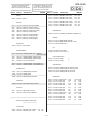
CPD-101VS
SERVICE MANUAL
US Model
Canadian Model
Chassis No. SCC-L19A-A
V-3 CHASSIS
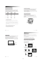
SPECIFICATIONS
Picture tube
0.25 mm aperture grille pitch,
15 inches measured diagonally
(14.0” viewable),
90-degree deflection,
AR coating
Viewable image size
Max. resolution
VESA standards
Approx. 285 × 214 mm (w/h)
(11 1/4 × 8 1/2 inches)
14.0” viewing image
(measured diagonally)
Horizontal: Max. 1280 dots
Vertical: Max. 1024 lines
640 × 480 at 85 Hz
800 × 600 at 85 Hz
1024 × 768 at 85 Hz
1280 × 1024 at 60 Hz
Deflection frequency
Horizontal: 30 to 70 kHz
Vertical: 50 to 120 Hz
Left, right: 3.0 W × 2
50 Hz – 20 kHz
Uni-directional, electret condenser
microphone
Speaker
Microphones
Microphones output
Audio input
3.5 mm miniplug
3.5 mm Stereo miniplug,
input impedance 47 kΩ,
input level 0.7 Vrms typical
Headphones output
Stereo minijack, 15 mW + 15 mW at
16 Ω
Subwoofer output 3.5 mm miniplug, volume variable
Controls
Front panel direct:
Audio volume/Contrast/Audio
mute/GPE (AUTO/off/mode 1/
mode 2)
OSD menu:
Brightness/Contrast/Picture size/
Picture zoom/Picture centering/
Sceen moiré/Color temperature
(5000K/6500K/9300K/11000K)/
Rotation/Pincushion/Pin balance/
Keystone/Key balance/Bass boost/
Manual Degauss/OSD position/
OSD language
AC input voltage/current
100 to 240 V, 50 – 60 Hz, 1.1 – 0.6 A
Power consumption
Max. 110 W
Dimensions
Approx. 368 × 408 × 388 mm
(w/h/d)
(14 1/2 × 16 1/8 × 15 3/8 inches)
Mass
Approx. 15.3 kg (33 lb 12 oz)
Design and specifications are subject to change without
notice.
TRINITRON MULTIMEDIA COMPUTER DISPLAY
®
MICROFILM
CPD-101VS
DIAGNOSIS
Failure
Power LED
+B Failure
Blink Amber (On 0.5 sec, Off 0.5 sec)
H Stop or V Stop Failure
Blink Amber (On 1.5 sec, Off 0.5 sec)
(Included S-Cap Failure)
ABL Failure
Blink Amber (On 0.5 sec, Off 1.5 sec)
Aging/Self-Test
Blink Amber (On 0.5 sec, Off 0.5 sec) .... Blink Green (On 0.5 sec, Off 0.5 sec)
Out of Range
On Green (OSD Indication)
TIMING SPECIFICATION
PRIMARY MODE
MODE AT PRODUCTION
PRIMARY
MODE 1
MODE 2
MODE 3
MODE 4
MODE 5
MODE 6
MODE 7
MODE 8
MODE 9
640 X 480
800 X 600
800 X 600
1024 X 768
1024 X 768
1280 X 1024
640 X 400
640 X 480
1152 X 864
36.000 MHZ
40.000 MHZ
49.500 MHZ
78.750 MHZ
94.500 MHZ
108.500 MHZ
25.175 MHZ
25.175 MHZ
80.000 MHZ
43.269 kHz
37.879 kHz
46.875 kHz
60.023 kHz
68.677 kHz
63.974 kHz
31.469 kHz
31.469 kHz
54.945 kHz
usec
usec
usec
usec
usec
usec
usec
usec
usec
H. TOTAL
23.111
26.4
21.333
16.66
14.561
15.631
31.778
31.778
18.2
H. BLK
5.333
6.4
5.172
3.657
3.725
3.834
6.356
6.356
3.8
H. FP
1.556
1
0.323
0.203
0.508
0.59
0.636
0.636
0.8
H. SYNC
1.556
3.2
1.616
1.219
1.016
1.18
3.813
3.813
1.4
H. BP
2.222
2.2
3.232
2.235
2.201
2.065
1.907
1.907
1.6
H. ACTIV
17.778
20
16.162
13.003
10.836
11.797
25.422
25.422
14.4
85.008 Hz
60.317 Hz
75.000 Hz
75.029 Hz
84.997 Hz
60.013 Hz
70.086 Hz
59.940 Hz
59.984 Hz
lines
lines
lines
lines
lines
lines
lines
lines
lines
V. TOTAL
509
628
625
800
808
1066
449
525
916
V. BLK
29
28
25
32
40
42
49
45
52
V. FP
1
1
1
1
1
1
12
10
6
V. SYNC
3
4
3
3
3
3
2
2
5
V. BP
25
23
21
28
36
38
35
33
41
V. ACTIV
480
600
600
768
768
1024
400
480
864
RESOLUTION
CLOCK
— HORIZONTAL —
H-FREQ
— VERTICAL —
V. FREQ(HZ)
— SYNC —
INT(G)
EXT(H/V)/POLARITY
EXT(CS)/POLARITY
INT/NON INT
NO
NO
NO
NO
NO
NO
NO
NO
NO
YES -/-
YES +/+
YES +/+
NO +/+
YES +/+
YES +/+
YES -/+
YES -/-
YES +/+
NO
NO
NO
NO
NO
NO
NO
NO
NO
NON INT
NON INT
NON INT
NON INT
NON INT
NON INT
NON INT
NON INT
NON INT
98.4.27 VER.
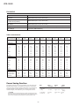
Power Saving Function
This display meets the power saving guidelines set by the International
ENERGY STAR Program. It is capable of reduced power consumption
when used with a computer equipped with Display Power Management
Signaling (DPMS). By sensing the absence of the sync signal coming
from the computer, it will reduce the power consumption as follows:
✔
CAUTION
The Power Saving function will automatically put the display into Deep Sleep mode if the
power switch is turned on without any video signal input. Once the horizontal and vertical
syncs are sensed, the display will automatically return to its Normal Operation mode.
–2–
Mode
1 Normal
Operation
2 Sleep
3 Deep Sleep
4 Power-off
Power
consumption
110 W (max)
Recovery
time
—
u Power
indicator
Green
15 W (max)
Approx. 3 sec.
8 W (max)
0W
Approx. 10 sec.
—
Green ˜
Orange
Orange
Off
SAFETY CHECK-OUT
CPD-101VS
(US Model only)
After correcting the original service problem, perform the following safety checks before releasing the set to the customer:
1. Check the area of your repair for unsoldered or poorly-soldered connections. Check the entire board surface for solder
splashes and bridges.
2. Check the interboard wiring to ensure that no wires are
“pinched” or contact high-wattage resistors.
3. Check that all control knobs, shields, covers, ground straps,
and mounting hardware have been replaced. Be absolutely
certain that you have replaced all the insulators.
4. Look for unauthorized replacement parts, particularly transistors, that were installed during a previous repair. Point
them out to the customer and recommend their replacement.
5. Look for parts which, though functioning, show obvious
signs of deterioration. Point them out to the customer and
recommend their replacement.
6. Check the line cords for cracks and abrasion. Recommend
the replacement of any such line cord to the customer.
7. Check the B+ and HV to see if they are specified values.
Make sure your instruments are accurate; be suspicious of
your HV meter if sets always have low HV.
8. Check the antenna terminals, metal trim, “metallized”
knobs, screws, and all other exposed metal parts for AC
Leakage. Check leakage as described below.
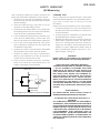
To Exposed Metal
Parts on Set
0.15 µF
1.5 k Ω
AC
Voltmeter
(0.75 V)
Earth Ground
Fig. A. Using an AC voltmeter to check AC leakage.
LEAKAGE TEST
The AC leakage from any exposed metal part to earth ground
and from all exposed metal parts to any exposed metal part having a return to chassis, must not exceed 0.5 mA (500
microampers).
Leakage current can be measured by any one of three methods.
1. A commercial leakage tester, such as the Simpson 229 or
RCA WT-540A. Follow the manufacturers’ instructions to
use these instruments.
2. A battery-operated AC milliammeter. The Data Precision
245 digital multimeter is suitable for this job.
3. Measuring the voltage drop across a resistor by means of a
VOM or battery-operated AC voltmeter. The “limit” indication is 0.75 V, so analog meters must have an accurate lowvoltage scale. The Simpson 250 and Sanwa SH-63Trd are
examples of a passive VOMs that are suitable. Nearly all
battery operated digital multimeters that have a 2 V AC
range are suitable. (See Fig. A)
WARNING!!
NEVER TURN ON THE POWER IN A CONDITION IN
WHICH THE DEGAUSS COIL HAS BEEN REMOVED.
SAFETY-RELATED COMPONENT WARNING!!
COMPONENTS IDENTIFIED BY SHADING AND MARK
¡ ON THE SCHEMATIC DIAGRAMS, EXPLODED
VIEWS AND IN THE PARTS LIST ARE CRITICAL FOR
SAFE OPERATION. REPLACE THESE COMPONENTS
WITH SONY PARTS WHOSE PART NUMBERS APPEAR AS SHOWN IN THIS MANUAL OR IN SUPPLEMENTS PUBLISHED BY SONY. CIRCUIT ADJUSTMENTS THAT ARE CRITICAL FOR SAFE OPERATION
ARE IDENTIFIED IN THIS MANUAL. FOLLOW THESE
PROCEDURES WHENEVER CRITICAL COMPONENTS
ARE REPLACED OR IMPROPER OPERATION IS SUSPECTED.
AVERTISSEMENT!!
NE JAMAIS METTRE SOUS TENSION QUAND LA
BOBINE DE DEMAGNETISATION EST ENLEVÉE.
ATTENTION AUX COMPOSANTS RELATIFS À LA
SÉCURITÉ!!
LES COMPOSANTS IDENTIFIÉS PAR UNE TRAME ET
UNE MARQUE ¡ SONT CRITIQUES POUR LA SÉCURITÉ.
NE LES REMPLACER QUE PAR UNE PIÈCE PORTANT LE
NUMÉRO SPECIFIÉ. LES RÉGLAGES DE CIRCUIT DONT
L’IMPORTANCE EST CRITIQUE POUR LA SÉCURITÉ DU
FONCTIONNEMENT SONT IDENTIFIÉS DANS LE
PRÉSENT MANUEL. SUIVRE CES PROCÉDURES LORS
DE CHAQUE REMPLACEMENT DE COMPOSANTS CRITIQUES, OU LORSQU’UN MAUVAIS FONCTIONNE-MENT
EST SUSPECTÉ.
–3–
CPD-101VS
TABLE OF CONTENTS
Section
Title
Page
1. GENERAL .................................................................. 1-1
2. DISASSEMBLY
2-1.
2-2.
2-3.
2-4.
2-5.
2-6.
2-7.
Cabinet Removal .................................................
Service Position ...................................................
D Board Removal .................................................
U Board Removal .................................................
J Board Removal ..................................................
Picture Tube Removal ..........................................
Harnes Location ...................................................
2-1
2-1
2-2
2-2
2-3
2-4
2-5
3. SAFETY RELATED ADJUSTMENT ............. 3-1
4. ADJUSTMENTS ...................................................... 4-1
5. DIAGRAMS
5-1. Block Diagrams ................................................... 5-1
5-2. Frame Schematic Diagram .................................. 5-5
5-3. Circuit Boards Location ...................................... 5-7
5-4. Schematic Diagrams and Printed Wiring Boards ... 5-7
(1) Schematic Diagram of A Board .......................... 5-11
(2) Schematic Diagrams of D Board ......................... 5-17
(3) Schematic Diagrams of AA, DA, J
and U Boards ........................................................ 5-21
5-5. Semiconductors ................................................... 5-26
6. EXPLODED VIEWS
6-1.
6-2.
6-3.
Chassis ................................................................. 6-1
Stand Block .......................................................... 6-2
Packing Materials ................................................ 6-3
7. ELECTRICAL PARTS LIST ............................ 7-1
–4–
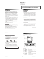
SECTION 1
GENERAL
The operating instructions mentioned here are partial abstracts
from the Operating Instruction Manual. The page numbers of
the Operating Instruction Manual remein as in the manual.
Introduction
Precautions
Congratulations on your purchase of a Sony Multimedia CPD-101VS
display!
This display incorporates over 25 years of Sony experience with Trinitron
display technology, ensuring excellent performance and outstanding
reliability.
This display’s wide scan range (30 – 70 kHz), together with Digital
Multiscan Technology, allows it to sync to any video mode from
standard VGA through VESA 1024 × 768 at 85 Hz (VESA 1280 × 1024 at
60 Hz).
In addition, its four factory-preset color modes give you unprecedented
flexibility in matching on-screen colors to hard copy printouts.
Furthermore, it features:
• Graphic Picture Enhancement function
improves monitor performance to match the application that you are
running.
With the GPE AUTO MODE, you can use “IntelliLight” compatible
software which will maximize the color and brightness of a window
running a multimedia presentation without affecting the brightness
and contrast of text based applications.
• Integrated stereo speakers with Bass Boost
enables you to enjoy excellent sound reproduction via 3.0 W stereo
speakers.
All together, CPD-101VS delivers incredible performance with the
quality and support you can expect from Sony.
Installation
• Prevent internal heat build-up by allowing adequate air circulation.
Do not place the unit on surfaces (rugs, blankets, etc.) or near
materials (curtains, draperies) that may block the ventilation holes.
• Do not install the unit near heat sources such as radiators or air ducts,
nor in a place subject to direct sunlight, excessive dust, mechanical
vibration or shock.
• Do not place the unit near equipment which generates magnetism,
such as a converter or high voltage power lines.
Maintenance
• Clean the cabinet, glass panel and controls with a soft cloth lightly
moistened with a mild detergent solution. Do not use any type of
abrasive pad, scouring powder or solvent, such as alcohol or benzine.
• Do not rub, touch, or tap the surface of the screen with sharp or
abrasive items, like a ball point pen or a screwdriver, as this type of
contact may result in a scratched picture tube.
Transportation
• Do not discard the carton and packing materials. When transporting
the unit, use these packing materials so that the unit is properly
packaged.
• When carrying the unit, be careful not to get your hands caught
between the display and the tilt-swivel.
Plug and play
This display complies with DDC™1 and DDC2B which are the Display
Data Channel (DDC) standards of VESA.
When a DDC1 host system is connected, the display synchronizes with
the V. CLK in accordance with the VESA standards and outputs the
EDID (Extended Display Identification Data) to the data line.
When a DDC2B host system is connected, the display automatically
switches to DDC2B communication.
Continued to the next page ➔
DDC™ is a trademark of Video Electronics Standard Association.
6
Introduction
7
Precautions
Functions of Controls
Front
Warning on Power Connection
• Use the supplied power cord.
For the customers in U.S.A.
If you do not do this, this display will not conform to mandatory FCC
standards.
For the customers in UK.
If you use the display in the UK, please use the supplied UK cable
with the UK plug.
for 100 to 120 V AC
for 220 to 240 V AC
1
2
3
for 240 V AC only
• Before disconnecting the power cord, wait at least 30 seconds after
turning off the power switch to discharge static electricity from the
CRT display surface.
• After the power has been turned on, the CRT is demagnetized for
approximately 5 seconds. This generates a strong magnetic field
around the bezel which may affect the data stored on magnetic tape or
disks near the bezel. Place such magnetic recording equipment and
tapes/disks at a distance from this unit.
45 6
7 8 9
!º
The socket-outlet shall be installed near the equipment and shall be
easily accessible.
1
2
3
4
5
6
7
8
9
!º
8
Precautions
1-1
Microphone
Screen
Stereo speakers
¤ Mute button
? Reset switch
GPE button and
indicator
. Volume +/–
buttons
MENU button
> +/– Contrast
buttons
U Power switch
and indicator
—
—
—
Mutes sound (page 20).
Resets adjustments to factory setting (page 30).
Sets GPE mode (page 31).
Adjust speaker volume (page 19). The default
setting of the volume level is 30 %. Use to select
items in an OSD.
Displays the OSD menu.
Adjust picture contrast (page 21). Use to adjust
items in an OSD.
Turns the display on and off.
Functions of Controls
9
Getting Started
Rear
Before using this display, please make sure that the following items are
included in your package:
• Multimedia CPD-101VS display (1)
• Power cord (1)
• Warranty card (1)
• Operating instructions manual (1)
• Windows 95/98 Monitor Information Disk and its instruction manual
(1)
✎
Tip
This display will sync with any IBM or compatible system equipped with VGA1) or greater
graphics capability. Although this display will sync to other platforms running at horizontal
frequencies between 30 and 70 kHz, including Macintosh2) and Power Macintosh systems, a
cable adapter is required. Please consult Sony Technical Support for advice on which adapter is
suitable for your needs.
!¡
!™
!∞
!£
!§
!¢
!¶
!¡
!™
AC IN connector
2 Audio plug (green)
!£
h MIC plug (red)
!¢
; Video signal cable
(blue)
2 Headphones jack
!∞
!§
!¶
10
Tilt-Swivel
Subwoofer output
jack
1) VGA is a trademark of IBM Corporation.
2) Macintosh is a trademark of Apple Computer Inc.
Continued to the next page ➔
Connect the supplied power cord (page 13).
Connect to the computer’s audio output
(page 12).
Connect to the computer’s microphone input
(page 12).
Connect to the computer’s video output
(page 12).
Connect standard mini-plug headphones (not
supplied). The speakers are turned off when
headphones are connected.
Adjusts the angle of the display (page 15).
Connect to a subwoofer’s input jack (not
supplied).
Functions of Controls
Getting Started
p Step 2: Connect the power cord
Installation
With the display switched off, connect the power cord to the display
and the other end to a power outlet.
p Step 1: Connect the computer
With the computer switched off, connect the video signal cable to the
display (VGA) connector on your computer. If your computer supports
the DDC plug-and-play standard, this connection will enable DDC
communication between the display and the computer.
The video signal cable is combined with audio and microphone cables.
If your computer is equipped with sound capability, connect the audio
(green) and microphone (red) plugs to appropriate jacks located on your
computer.
to a power outlet
Power cord (supplied)
p Step 3: Turn on the display, and then your
computer.
2
PRINTER
Blue (to monitor
connector)
11
AL
USB
For proper Plug and Play recognition, turn on the display before you
turn on your computer.
CONTR
MONITOR
LINE OUT LINE IN
Green (to LINE OUT
connector)
MIC
Fasten the
screw of the
blue plug.
✔
Note on Warning Messages
If there is something wrong with the input signal, one of the following messages appears.
“OUT OF SCAN RANGE”
This indicates that the input signal is not supported by the display’s specifications.
Red (to microphone
connector)
“NO INPUT SIGNAL”
This indicates that video signal is missing.
To solve these problems, see “Troubleshooting” on page 35.
p Step 4: If necessary...
Computer
Adjust the user controls according to your personal preference.
The installation of your display is complete. Enjoy your display.
✔
Note on handling the video signal cable
Do not touch the pins of the video signal cable.
12
Getting Started
Getting Started
1-2
13
Using Your Display
p To enter new timings
Preset and user modes
When using a video mode that is not one of the 9 factory preset modes,
some fine tuning may be required to optimize the display to your
preferences. Simply adjust the display according to the adjustment
instructions. The adjustments will be stored automatically and recalled
whenever that mode is used.
A total of 16 user-defined modes can be stored in memory. If a 17th mode
is entered, it will replace the first.
The Multimedia CPD-101VS display has factory preset modes for the 9
most popular industry standards for true “plug and play” capability.
For less common modes, its Digital Multiscan Technology will perform
all of the complex adjustments necessary to ensure a high quality picture
for any timing between 30 and 70␣ kHz.
NO.
Resolution
(dots × lines)
640 × 400
640 × 480
640 × 480
800 × 600
800 × 600
1024 × 768
1024 × 768
1152 × 864
1280 × 1024
1
2
3
4
5
6
7
8
9
Horizontal
Frequency
31.5 kHz
31.5 kHz
43.3 kHz
37.9 kHz
46.9 kHz
60.0 kHz
68.7 kHz
54.8 kHz
64.0 kHz
Vertical
Frequency
70 Hz
60 Hz
85 Hz
60 Hz
75 Hz
75 Hz
85 Hz
60 Hz
60 Hz
Using the tilt-swivel
With the tilt-swivel, this unit can be adjusted to be viewed at your
desired angle within 90° horizontally and 7° vertically.
To turn the unit vertically and horizontally, hold it at its bottom with
both hands.
Be careful not to get your hands caught between the display and the tiltswivel.
✔
Note for Windows® 95/98 users
Install the new model information of the Sony computer display from “Windows 95/98
Monitor Information disk” into your PC. (To install the file, refer to the attached “About the
Windows 95/98 Monitor Infomration Disk”.)
45˚
7˚
45˚
This display complies with “VESA DDC,” the standards of Plug & Play. If your PC/graphic board
complies with DDC, select “Plug & Play Display (VESA DDC)” or this display’s model name
(CPD-101VS) as “Display type” from “Control Panel” in Windows 95/98. Some PC/graphic
boards do not comply with DDC. Even if they comply with DDC, that may have some problems
connecting this display. In this case, select this display’s model name (CPD-101VS) as “Display
type” in Windows 95/98.
Windows® is a registered trademark of Microsoft Corporation in the United States and other
countries.
✔
Note on recommended horizontal timing conditions
Horizontal sync width should be more than 1.0 µsec.
Horizontal blanking width should be more than 3.6 µsec.
14
Using Your Display
Using Your Display
15
Adjustments
When one of the preset-type signals is input, no picture adjustment is
necessary.
You can, however, adjust the picture to your preference by following the
procedure described below.
Damper wire
Using a white background, a very thin horizontal line on the screen may
be visible as shown below. This line is the damper wire.
The Trinitron tube has a vertically striped Aperture Grille inside. The
Aperture Grille allows more light to pass through to the screen giving
the Trinitron CRT more color and brightness.
The damper wire is attached to the Aperture Grille to prevent vibration
of the Aperture Grille wire so that the screen image is constantly stable.
To adjust the display, turn on the display and computer.
Introducing the On-Screen Display
Beyond sound volume and picture contrast adjustment, most
adjustments are made using the OSD menu system.
Using the OSD menu
Damper wire
1. Press the MENU button to display the MENU OSD.
MENU
Approx. 6 cm
(2 3/8 inches)
OK
MENU
COLOR CENTER SCREEN
BRIGHT
EXIT
ZOOM
GEOM
SIZE
OPTION
2. Use the the four arrow (>/./?//) buttons (. +/– and > +/–
buttons) to select the item you want to adjust.
Change the item from blue to yellow.
MENU
OK
MENU
COLOR CENTER SCREEN
BRIGHT
EXIT
ZOOM
GEOM
SIZE
OPTION
3. Press the MENU button again.
The item is selected and the item’s OSD appears.
BRIGHT/CONTRAST
50
BRIGHTNESS
16
Using Your Display
Adjustments
1-3
17
Summary of each item
1
2
MENU
9
8
Adjusting the sound volume
3
OK
1. Press the . + or – button.
MENU
The VOLUME/CONTRAST OSD appears.
The horizontal and vertical frequencies for each input signal received
appear.
COLOR CENTER SCREEN
BRIGHT
EXIT
ZOOM
GEOM
SIZE
OPTION
7
6
5
VOLUME/CONTRAST
4
26
65. 0kHz /
Horizontal
frequency
1 COLOR
Selects the color temperature.
26
76Hz
Vertical
frequency
2. Press the . +/– buttons to adjust volume.
+ to increase volume
– to decrease volume
2 CENTER
Adjusts the picture centering.
3 SCREEN
Reduces the moiré pattern.
4 ZOOM
Adjusts the picture size in horizontal and vertical direction
proportionally.
The VOLUME/CONTRAST OSD disappears three seconds after you
release the buttons.
5 OPTION
Activates bass-boost and screen degauss, changes the OSD position
and selects the OSD language.
✎ Tips
• The default setting of the volume level is 30 %.
• Adjust the volume while listening to the sound.
• Excessively high volume may cause howling.
6 SIZE
Adjusts the picture size. You can adjust the size in horizontal or
vertical direction individually.
p To activate Bass Boost for rich bass sound
7 GEOM
Adjusts the picture rotation, pincushion, etc.
1. Select OPTION in the MENU OSD and press the MENU button.
The OPTION OSD appears.
8 BRIGHT
Adjusts the picture brightness and contrast.
MENU
OK
OPTION
MENU
OFF
9 EXIT
Closes the OSD menu.
ON
COLOR CENTER SCREEN
BRIGHT
EXIT
ZOOM
GEOM
SIZE
OPTION
BASS BOOST
Continued to the next page ➔
18
Adjustments
Adjustments
2. Select BASS BOOST with the >/. buttons.
Adjusting the picture contrast
3. Press the / button to select ON.
The adjustment data becomes the common setting for all input signals.
To cancel bass boost, press the ? button to select OFF.
OPTION
OFF
19
1. Press the > + or – button.
ON
The VOLUME/CONTRAST OSD appears.
The horizontal and vertical frequencies for each input signal received
appear.
VOLUME/CONTRAST
BASS BOOST
26
To exit the OSD
Press the MENU button again.
65. 0kHz /
✎
Horizontal
frequency
Tip
If you don’t touch any buttons, the OSD automatically disappears after 30 seconds.
26
76Hz
Vertical
frequency
2. Press the > +/– buttons to adjust the picture contrast.
+ for more contrast
– for less contrast
p To mute the sound
Press the ¤ button. The ¤ indicator appears while the sound is muted.
The VOLUME/CONTRAST OSD disappears three seconds after you
release the buttons.
Press again to cancel muting.
You can cancel muting also by pressing the . + button.
✎
Tip
¤ appears instead of . on the VOLUME/CONTRAST OSD while the sound is muted.
Adjusting the picture brightness
The adjustment data becomes the common setting for all input signals.
1. Select BRIGHT in the MENU OSD and press the MENU button.
The BRIGHT/CONTRAST OSD appears.
MENU
OK
MENU
COLOR CENTER SCREEN
BRIGHT
EXIT
ZOOM
GEOM
SIZE
OPTION
BRIGHT/CONTRAST
50
BRIGHTNESS
Continued to the next page ➔
20
Adjustments
Adjustments
1-4
21
✎ Tip
2. Press the ?// buttons to adjust the picture brightness.
If you don’t touch any buttons, the OSD automatically disappears after 30 seconds.
/ for more brightness
? for less brightness
Adjusting the picture size
The adjustment data becomes the individual setting for each input signal
received.
To adjust the picture size in horizontal and vertical direction
proportionally
To exit the OSD
Press the MENU button again.
✎
1. Select ZOOM in the MENU OSD and press the MENU button.
Tip
If you don’t touch any buttons the OSD automatically disappears after 30 seconds.
The ZOOM OSD appears.
MENU
OK
MENU
ZOOM
COLOR CENTER SCREEN
Adjusting the picture centering
The adjustment data becomes the individual setting for each input signal
received.
1. Select CENTER in the MENU OSD and press the MENU button.
OK
MENU
EXIT
ZOOM
GEOM
SIZE
OPTION
H
V
74
49
2. Press the ?// buttons for the best size.
The CENTER OSD appears.
MENU
BRIGHT
CENTER
COLOR CENTER SCREEN
73
BRIGHT
EXIT
ZOOM
GEOM
SIZE
OPTION
26
2. For vertical adjustment
Press the >/. buttons.
> to move up
. to move down
To adjust the picture size in horizontal or vertical direction
1. Select SIZE in the MENU OSD and press the MENU button.
For horizontal adjustment
Press the ?// buttons.
/ to move right
? to move left
The SIZE OSD appears.
MENU
OK
MENU
SIZE
COLOR CENTER SCREEN
73
BRIGHT
EXIT
ZOOM
GEOM
SIZE
OPTION
26
To exit the OSD
Press the MENU button again.
22
Continued to the next page ➔
Adjustments
Adjustments
2. For vertical adjustment
Press the >/. buttons.
> to increase
. to decrease
For horizontal adjustment
Press the ?// buttons.
/ to increase
? to decrease
3. Press the ?// buttons to adjust.
To exit the OSD
Press the MENU button again.
✎
Tip
If you don’t touch any buttons, the OSD automatically disappears after 30 seconds.
Adjusting the geometry
The rotation adjustment data becomes the common setting for all input
signals. All other data becomes the individual setting for each input
signal received.
MENU
/ to rotate the picture
clockwise
? to rotate
counterclockwise
PINCUSHION
/ to bend both
sides outward
? to bend inward
PIN BALANCE
/ to bend both sides
to the right
? to the left
KEYSTONE
/ to widen the top
? to shrink the top
KEY BALANCE
/ to move the top to
the right
? to the left.
✎
Tip
If you don’t touch any buttons, the OSD automatically disappears after 30 seconds.
The GEOMETRY OSD appears.
OK
ROTATION
To exit the OSD
Press the MENU button again.
1. Select GEOM in the MENU OSD and press the MENU button.
MENU
23
GEOMETRY
COLOR CENTER SCREEN
BRIGHT
EXIT
ZOOM
GEOM
SIZE
OPTION
Selecting the color temperature
26
The selected color temperature becomes the common setting for all input
signals.
ROTATION
1. Select COLOR in the MENU OSD and press the MENU button.
2. Press the >/. buttons to select the item you want to adjust.
The COLOR OSD appears.
MENU
OK
MENU
COLOR CENTER SCREEN
BRIGHT
EXIT
ZOOM
GEOM
SIZE
OPTION
COLOR
11000K
9300K
6500K
5000K
Continued to the next page ➔
24
Adjustments
Adjustments
1-5
25
3. Press the . button to select MOIRE ADJUST.
2. Select the desired color temperature with the >/. buttons.
11000K for the brightest white
9300K for TV white
6500K for video monitor white
5000K for printing paper white
SCREEN
26
To exit the OSD
Press the MENU button again.
MOIRE ADJUST
✎
4. Press the ?// buttons to tune the moiré cancellation effect.
Tip
If you don’t touch any buttons, the OSD automatically disappears after 30 seconds.
To exit the OSD
Press the MENU button again.
✎
Adjusting the screen moiré
Tip
If you don’t touch any buttons, the OSD automatically disappears after 30 seconds.
This adjustment is to eliminate wavy or elliptical lines that may appear
on the screen.
The adjustment data becomes the common setting for all input signals.
✔
Note on the moiré cancellation effect
When CANCEL MOIRE is set to ON, the picture may appear fuzzy. If you set CANCEL
MOIRE to OFF, the picture may be clearer, but the moiré will reappear.
1. Select SCREEN in the MENU OSD and press the MENU button.
The SCREEN OSD appears.
MENU
OK
SCREEN
MENU
OFF
Activating screen degauss
ON
COLOR CENTER SCREEN
BRIGHT
EXIT
ZOOM
GEOM
SIZE
OPTION
The display screen is automatically degaussed (demagnetized) when the
power is turned on.
To manually degauss the screen, do as follows. If you need to degauss
the screen a second time, wait at least 20 minutes for the best result.
CANCEL MOIRE
1. Select OPTION in the MENU OSD and press the MENU button.
2. Press the / button to select ON.
The OPTION OSD appears.
The MOIRE ADJUST icon appears under the CANCEL MOIRE icon.
MENU
OFF
OK
OPTION
MENU
OFF
SCREEN
ON
COLOR CENTER SCREEN
ON
BRIGHT
EXIT
ZOOM
GEOM
SIZE
OPTION
BASS BOOST
CANCEL MOIRE
Continued to the next page ➔
26
Adjustments
Adjustments
2. Select MANUAL DEGAUSS with the >/. buttons.
27
3. Press the ?// buttons to move the OPTION OSD to the desired
position.
OPTION
ON
MANUAL DEGAUSS
To exit the OSD
Press the MENU button again.
3. Press the / button to activate the degauss cycle.
✎ Tip
To exit the OSD
Press the MENU button again.
If you don’t touch any buttons, the OSD automatically disappears after 30 seconds.
✎
Tip
If you don’t touch any buttons, the OSD automatically disappears after 30 seconds.
Selecting the OSD language
English, French, German, Spanish and Japanese version of the OSDs are
available.
Changing the OSD position
1. Select OPTION in the MENU OSD and press the MENU button.
1. Select OPTION in the MENU OSD and press the MENU button.
The OPTION OSD appears.
The OPTION OSD appears.
MENU
OK
MENU
MENU
OK
OPTION
MENU
OPTION
OFF
OFF
ON
COLOR CENTER SCREEN
ON
COLOR CENTER SCREEN
BRIGHT
EXIT
SIZE
EXIT
ZOOM
GEOM
SIZE
OPTION
BASS BOOST
BASS BOOST
GEOM
BRIGHT
ZOOM
OPTION
2. Select LANGUAGE with the >/. buttons.
2. Select OSD H (horizontal) POSITION or OSD V (vertical) POSITION
OPTION
with the >/. buttons.
OPTION
OPTION
ENG FRA DEU
ESP
LANGUAGE
OSD H POSITION
OSD V POSITION
Continued to the next page ➔
28
Adjustments
Adjustments
1-6
29
Graphic Picture Enhancement (GPE)
3. Press the ?// buttons to select the desired language.
Available GPE modes
Graphic Picture Enhancement is a function designed for your viewing
comfort.
There are four GPE modes: AUTO, MODE 1, MODE 2 and OFF.
The default setting is “AUTO.”
To exit the OSD
Press the MENU button again.
p AUTO mode
This mode is effective only with “IntelliLight” compatible applications.
When an image playback window with “IntelliLight” coding appears on
the screen, the display senses the exact location and size of the window
and applies a higher brightness and sharpness effect to images inside the
window, while the rest of the screen remains at standard picture quality.
For inquiries about “IntelliLight” and compatible software, check Sony’s
web site (www.ita.sel.sony.com) or call Sony Technical Support (1-8884SONYPC).
✎ Tip
If you don’t touch any buttons, the OSD automatically disappears after 30 seconds.
Resetting
“IntelliLight” is a trademark of Sony Electronics Inc.
p To recall the factory settings for an individual
adjustment item
1. Select the item you want to reset.
Window with “IntelliLight” coding has
higher brightness and sharpness.
First select the OSD containing the item in the MENU OSD, and then
select the item in the OSD.
Standard picture quality
2. Press the ? button while the OSD of the item is on.
Only the item highlighted in yellow returns to the factory setting.
✔
Note on the AUTO mode
If one of the four corners of the “IntelliLight” window is covered or if the window goes
beyond the screen border, the GPE effect turns off.
✎
Tip
You can adjust the picture contrast or brightness of the screen outside of the “IntelliLight”
window. The “IntelliLight” window always remains clear and sharp regardless of the
adjustments made to the rest of the screen.
p To recall the factory settings for the current
video mode
Press the ? button while no OSD is displayed.
p MODE 1
p To recall the factory settings for all modes
Higher contrast is applied across the entire screen. MODE 1 is designed
to enhance still image presentations.
Press and hold the ? button for more than two seconds.
All adjustments return to the factory settings.
✔
Note on MODE 1
Whenever the screen resolution is changed, power saving activated, or power turned off,
MODE 1 is cancelled and GPE returns to the AUTO mode.
30
Adjustments
Graphic Picture Enhancement (GPE)
31
Power Saving Function
p MODE 2
This display meets the power saving guidelines set by the International
ENERGY STAR Program. It is capable of reduced power consumption
when used with a computer equipped with Display Power Management
Signaling (DPMS). By sensing the absence of the sync signal coming
from the computer, it will reduce the power consumption as follows:
Higher contrast and sharpness is applied across the entire screen.
MODE 2 is designed to enhance graphic games and movie/video
presentations.
✔Note on MODE 2
✔
Whenever the screen resolution is changed, power saving activated, or power turned off,
MODE 2 is cancelled and GPE returns to the AUTO mode.
CAUTION
The Power Saving function will automatically put the display into Deep Sleep mode if the
power switch is turned on without any video signal input. Once the horizontal and vertical
syncs are sensed, the display will automatically return to its Normal Operation mode.
✎ Tip
MODE 2 may produce ghost images when displaying text oriented applications. In this
case, select the AUTO or OFF mode.
Mode
p GPE OFF mode
1 Normal
Operation
2 Sleep
Screen sharpness and brightness are set to standard quality without any
additional enhancements. This mode is suited for text-based
applications.
✔Note on the GPE OFF mode
3 Deep Sleep
4 Power-off
Once OFF mode is selected, GPE status stays in the OFF mode until you manually select
other GPE modes.
Power
consumption
110 W (max)
Recovery
time
—
u Power
indicator
Green
15 W (max)
Approx. 3 sec.
8 W (max)
0W
Approx. 10 sec.
—
Green ˜
Orange
Orange
Off
Selecting the GPE mode
Press the GPE button repeatedly until the screen message of the desired
mode is displayed.
Each time you press the GPE button, the GPE mode changes as follows:
n
AUTO n GPE OFF n MODE 1 n MODE 2
AUTO
Appears for three seconds
The GPE indicator lights up when AUTO, MODE 1 or MODE 2 is
selected.
32
Graphic Picture Enhancement (GPE)
Power Saving Function
1-7
33
Troubleshooting
Howling (feedback) is heard
m Decrease the volume with . +/– buttons, or turn down the
microphone input volume of the sound board.
This section may help you isolate a problem and as a result, eliminate the
need to contact technical support, allowing continued productivity.
No picture
If the U indicator is not lit
m Check that the power cord is properly connected.
m Check that the U switch is in the “on” position.
Picture is scrambled
m Check your computer manual for the proper display setting.
m Check this manual and confirm that the graphic mode and the
frequency you are trying to operate is supported. Even if the
frequency is within the proper range, some video boards may have a
sync pulse that is too narrow for the display to sync correctly.
If the “NO INPUT SIGNAL” message appears on the screen, or if the U
indicator is either orange or alternating between green and orange
m Try pressing any key on the computer keyboard.
m Check that your computer power switch is in the “on” position.
m Check that the video signal cable is properly connected and all plugs
are firmly seated in their sockets.
m Ensure that no pins are bent or pushed in the HD15 video input
connector.
If the “OUT OF SCAN RANGE” message appears on the screen
m Check that the video frequency is within that specified for the display.
Horizontal: 30 – 70 kHz
Vertical: 50 – 120 Hz
Refer to your computer’s instruction manual to adjust the video
frequency range.
m If you are using a video signal cable adapter, check that it is the correct
one.
Color is not uniform
m Degauss the display (page 27).
If you place equipment which generates a magnetic field, such as a
speaker, near the display, or you change the direction of the display,
color may lose uniformity. The degauss function demagnetizes the
metal frame of the CRT to obtain a neutral field for uniform color
reproduction. If a second degauss cycle is needed, allow a minimum
interval of 20 minutes for the best result.
Screen image is not centered or sized properly
m Adjust the size or centering (pages 22, 23).
m Some video modes do not fill the screen to the edge. This problem
tends to occur with certain video boards.
Edges of the image are curved
m Adjust the geometry (page 24).
If no message is displayed and the U indicator is green or flashing orange
m See “Self-diagnosis function” (page 38).
Picture is fuzzy
m Adjust the contrast and brightness (page 21). Some brands of video
boards have an excessive video output level which creates a fuzzy
picture at maximum contrast.
m Degauss the display (page 27).
If you place equipment which generates a magnetic field, such as a
speaker, near the display, or you change the direction of the display,
color may lose uniformity. The degauss function demagnetizes the
metal frame of the CRT to obtain a neutral field for uniform color
reproduction. If a second degauss cycle is needed, allow a minimum
interval of 20 minutes for the best result.
m If moiré is cancelled, the picture may become fuzzy. Decrease the
moiré cancellation effect (page 26).
m If the GPE mode is set to AUTO, change it to OFF (page 32).
No sound from speaker
If the ¤ indicator is displayed
m Press the ¤ button to cancel muting.
m
m
m
m
Check that the audio plug is properly connected.
Adjust the volume with . +/– buttons.
Check that the headphones are not connected.
Check the volume control, muting, sound selector, etc. of the sound
board. (See the computer’s manual.)
Microphone mixing is not possible
m Check that the MIC plug is properly connected.
m Check the microphone control, sound selector, etc. of the sound board.
(See the computer’s manual.)
Continued to the next page ➔
Troubleshooting
36
35
Troubleshooting
A fine horizontal line (wire) is visible
m This wire stabilizes the vertically striped Aperture Grille (page 16).
This Aperture Grille allows more light to pass through to the screen
giving the Trinitron CRT more color and brightness.
Picture bounces or has wavy oscillations
m Isolate and eliminate any potential sources of electric or magnetic
fields. Common causes for this symptom are electric fans, fluorescent
lighting, laser printers, etc.
m If you have another display close to this display, increase the distance
between them to reduce interference.
m Try plugging the display into a different AC outlet, preferably on a
different circuit.
Hum is heard right after the power is turned on
m When the power is turned on, the Auto-degauss cycle is activated.
While the Auto-degauss cycle is activated, a hum may be heard. The
same hum is heard when the display is manually degaussed. This is
not a malfunction.
Picture is flickering
m Set the refresh rate on the computer to obtain the best possible picture
by referring to your computer’s manual.
m If the GPE mode is set to AUTO, change it to OFF (page 32).
• If the problem persists, call your authorized Sony dealer from a
location near you, or call Sony Technical Support at 1-888-4SONYPC
(1-888-476-6972).
• Note the model name and the serial number of your display. Also note
the make and name of your computer and video board.
Picture appears to be ghosting
m Eliminate the use of video extensions and/or video switch boxes if
this symptom occurs. Excessive cable length or weak connections can
produce this symptom.
m If the GPE mode is set to AUTO, change it to OFF (page 32).
m If the GPE mode is set to MODE 2, the picture may appear to be
ghosting. Set to another GPE mode (page 32).
Self-diagnosis function
Wavy or elliptical (moiré) pattern is visible
m Cancel the moiré (page 26).
The moiré may be modified depending on the connected computer.
m Due to the relationship between resolution, display dot pitch and the
pitch of some image patterns, certain screen backgrounds sometimes
show moiré. Change your desktop pattern.
This display is equipped with a self-diagnosis function. Use this function
if there is a problem with your display or computer.
1. Disconnect the video input cable or turn off the connected computer.
2. Turn the display off and on.
IntelliLight does not work
m Check that all four corners of the “IntelliLight” window are clearly
displayed and are not covered by another window.
m Check that the GPE mode is set to AUTO (page 32).
m Leave the display’s power “on” and reboot your computer.
m IntelliLight does not work correctly with an interlaced video mode.
Check the vertical refresh rate in the Properties window of Windows
95/98 and select a non-interlaced mode.
3. Press and hold the >/ button for more than 2 seconds.
If all four color bars appear (white, red, green, blue) after a few seconds,
the display is working properly, but there might be a problem with your
computer. Contact your computer’s manufacturer.
If the color bars do not appear, there might be a problem with the
display. Contact your local authorized Sony dealer, or call Sony Technical
Support at 1-888-4SONYPC (1-888-476-6972).
Tiny color bars appear in the corners of the IntelliLight window
m Set the GPE mode to AUTO (page 32).
m Check that all four corners of the “IntelliLight” window are clearly
displayed and are not covered by another window.
Continued to the next page ➔
Troubleshooting
37
38
1-8
Troubleshooting
CPD-101VS
SECTION 2
DISASSEMBLY
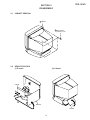
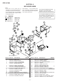
2-1. CABINET REMOVAL
2 Cabinet
1 Four screws
(+BVTP 4 x 16)
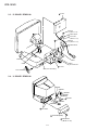
2-2. SERVICE POSITION
(1) D board
(2) U board
A block
1
3
2
D board
U board
2-1
CPD-101VS
2-3. D BOARD REMOVAL
1 A block
2 Screw
(+BVTT 4 x 8)
3 Cable stopper
6 Five screws
(+BVTP 3 x 12)
4 Screw
(+BVTP 3 x 12)
5 Cable blacket
CN904
GND
CN601
Not used screw
CN607
7 D board
GND (From stand assy)
From harness assy
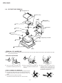
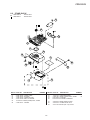
2-4. U BOARD REMOVAL
CN5204
CN5200
CN5202
CN5605
CN5606
4 U board
CN5601
CN5607
3 Two claws
2 Stand base (Rear)
1 Two screws
(+BVTP 4 x 16)
2-2
CPD-101VS
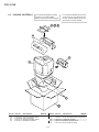
2-5. J BOARD REMOVAL
1 Two screws
(+BVTP 4 x 16)
5 J board
4 Screw
(+BVTP 3 x 12)
2 Seven screws
(+BVTP 4 x 16)
3 Stand base (Lower)
2-3
CPD-101VS
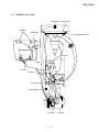
2-6. PICTURE TUBE REMOVAL
10 Demagnetization coil
11 Tension spring
CN601
3 Two screws
(+BVTP 4 x 16)
2 A block
CN314
CN302
CN303
5 Stand block
CN512
6 Neck assy
7 Deflection yoke
CN501
8 Four screws
2P
(Tapping screw 5)
4 Two claws
12 Two degaussing coil holders
1 Anode cap
9 Picture tube
13 Two degaussing coil holders
Cushion
• REMOVAL OF ANODE-CAP
NOTE: Short circuit the anode of the picture tube and the anode cap to the metal chassis, CRT shield or carbon painted on the CRT,
after removing the anode.
• REMOVING PROCEDURES
c
b
a
Anode Button
1 Turn up one side of the rubber cap in
2 Using a thumb pull up the rubber cap
3 When one side of the rubber cap is
the direction indicated by the arrow a.
firmly in the direction indicated by the
arrow b.
separated from the anode button, the
anode-cap can be removed by turning
up the rubber cap and pulling up it in
the direction of the arrow c.
• HOW TO HANDLE AN ANODE-CAP
1 Don’t hurt the surface of anode-caps with shartp shaped material!
2 Don’t press the rubber hardly not to hurt inside of anode-caps!
A material fitting called as shatter-hook terminal is built in the
rubber.
3 Don’t turn the foot of rubber over hardly!
The shatter-hook terminal will stick out or hurt the rubber.
2-4
CPD-101VS
2-7. HARNESS LOCATION
Microphone Picture tube
Speaker
Stand assy
Demagnetization coil
CN6002
CN6003
CN6001
CN5204
CN5601
CN5606
D board
CN5200
CN5202
CN902
CN5607
CN5605
CN503
J board
CN903
CN904
CN502
CN607
CN501
U board
CN512
DA board
AC inlet
CN601
FBT
Ferrite Bead
CN308
CN302
CN301
CN314
CN316
CN309
CN306
CN315
CN310
CN303
AA board
2-5
CN305
CN307
A board
CPD-101VS
SECTION 3
SAFETY RELATED ADJUSTMENT
• HV Protector Circuit Check
When replacing or repairing the shown below table, the
following operational checks must be performed as a
safety precaution against X-rays emissions from the unit.
Confirm that the voltage between cathode of D517 on D
board and GND is more than 17.5 V DC and Using external DC Power Supply, apply the voltage shown below
between cathode of D517 and GND, and confirm that
the HV HOLD DOWN circuite works. (TV Rester disappears)
Standard voltage : Less than 31.70 V DC
Part Replaced ([)
HV ADJ
RV501
Part Replaced (])
HV Regulator
Circuit Check
D board IC501, C553, C554,
C555, C558, C561,
R540, R564, R567,
RV501, T501 (FBT)
HV Hold-down
Circuit Check
D board IC603, IC901, D515,
D517, C540, C542,
C544, R543, R547,
R549, R552,
T501 (FBT)
Beam Current
Protector Circuit
Check
Check Condition
• Input voltage : 100 – 120 V AC
• Input signal : White Cross hatch at Max fH
• Beam control : CONT : 255, BRT : 80
• Beam Current Protector Check
Connect a variable resistor (20 kΩ or more) and an ammeter in series between FBT pin !] on D board and –15
V line. Decrease gradually the resistance of the variable
resistor from maximum to minimum, and confirm that
the Beam Current Protector Circuite works (TV Rester
disappears). The current must be within the range shown
below.
• Standard current : Less than 1.50 mA
D board IC603, IC604, IC901,
C535, C541, R515,
R545, R546, R548,
R550, R934,
T501 (FBT)
* Confirm one minute later turning on the power.
Check Condition
• Input voltage : 100 – 120 V AC
• Input signal : White Cross hatch at Max fH
• Beam control : CONT : 255, BRT : 80
• B+ Voltage Check
Standard voltage : 150.0 ± 3.0 V DC
Check Condition
• Input voltage : 100 – 120 V AC
Note : Use NF power supply or make sure that
distortion factor is 3% or less.
• Input signal : White Cross hatch at 64.0 kHz
• Beam control : CONT : 255, BRT : 80
3-1
CPD-101VS
SECTION 4
ADJUSTMENTS
• Landing Rough Adjustment
1. Enter the full white signal. (or the full black dots signal)
2. Set the contrast to “CONT”=MAX.
3. Make the screen monogreen.
Note: Off the outputs from R ch and B ch of SG.
4. Reverse the DY, and adjust coarsely the purity magnet (2pole Mg) so that a green raster positions in the center of
screen.
5. Moving the DY forward, adjust so that an entire screen becomes monogreen.
6. Adjust the tilt of DY, and fix lightly with a clamp.
Note: “TILT” shall be set at 0.
5. Attach the sensor of the landing adjustment unit on the CRT
surface.
Purity magnet position
<Neck Assy Zero Position>
Purity
Set the
finger
6. Adjust the DY position and purity, and the DY tilt.
L/D control specification
±5
±5
±5
• Landing Fine Adjustment
< Measurement condition >
Brightness : ∑Ik (520µA)
Magnetic field : BH=0, BV=45µT
CRT size : 270 × 202
Measurement point : 256 × 190
Temperature : 25ºC
a4
a5
a6
a7
a8
a9
8. Adjust each top and bottom pins by two wedges, and also
adjust swinging DY neck right-left by H.TILT and horizontal trapezoid, and then fix with two wedges.
(When fixing DY with wedges, insert wedges completely so
that the DY does not shake.)
[ µm ]
a
-—
a4
2
-—
a7
2
+—
a1
2
+ a4
—
2
Signal : Inverted crosshatch (Make the monogreen)
B
R
-—
a5
2
-—
a8
2
+—
a2
2
+ a5
—
2
+—
a8
2
-—
a3
2
-—
a6
2
-—
a9
2
+ a3
—
2
+ a6
—
2
+—
a9
2
1 minute
d “c” and “d” must be equal.
b
+—
a7
2
-—
a2
2
“a” and “b” must be equal, and
c
< Adjustment target>
After aging for 1 minute and more than 3 hours, adjust so
that it is exactly this value.
-—
a1
2
±5
±5
±5
7. Fasten DY with screw.
Note: Torque 22 ±2kgcm (2.2 ± 0.2 Nm)
Perform auto degaussing.
After aging for 9 minutes and more than 3 hours, adjust so
that it is exactly this value.
a1
a2
a3
±7
±7
±7
R
A
B
R
B
A1
R
B
B
B1
“A” and “B”,
“A1” and “B1”
must be equal.
<How to drive in wedges>
3 hours
L/D [ µm ]
+ ax
—
2
ax
0
-—
ax
2
1
180
9. If they do not satisfy the specification, connect the purity
magnet on DY and the disc magnet of the front and the rear
of DY located CRT side.
Note:
(1) When necessary to paste magnets more than 2 pieces, be
careful that the convergence and the distortion would be alterable.
(2) Paste within 80 to 120 mm from the DY on the diagonal line
of the magnet.
10. If using the magnet, be sure to demagnetize with the degausser and check.
11. Remove the sensor and wobbling coil.
12. Check that the DY is not tilting.
L/D Drift Curve
1. Put the set inside the Helmholtz coil.
2. Input the single green signal.
3. Demagnetize the CRT surface with the hand degausser , and
perform auto degaussing.
4. Attach the wobbling coil to the designated part of the CRT
neck.
4-1
CPD-101VS
Connect the communication cable of the computer to the connector located on the D board on the monitor. Run the service software
and then follow the instruction.
1 1-690-391-21
2 A-1500-819-A
Interface Unit
3 3-702-691-01
Connector Attachment
IBM AT Computer
as a Jig
To BUS CONNECTOR
D-sub
(9 Pin [female])
mini Din
(8Pin)
*The parts above ( 1
4 Pin
NECK Assy
4 Pin
3 ) are necessary for DAS adjustment.
• Convergence Specification
• Convergence Rough Adjustment
1. Enter the white crosshatch signal (white lines on black).
2. Adjust roughly the horizontal and vertical convergence at
four-pole magnet.
3. Adjust roughly HMC and VMC at six-pole magnet.
Standard: ± 0.1mm (In the center of screen)
B
MODE
All mode
A
A
0.24 mm
B
0.30 mm
XBV
• White Balance Adjustment Specification
(1) 1100K
(2) 9300K
x = 0.274 ± 0.008
x = 0.283 ± 0.008
y = 0.287 ± 0.008
y = 0.298 ± 0.008
(3) 5000K
x = 0.345 ± 0.008
y = 0.358 ± 0.008
XCV
P.S Mg
Six-Pole Mg
4 Pin
DY
CRT
YCH
TLV
Four-Pole Mg
Fig. 1
XCV
Fig. 2
• Vertical and Horizontal Position and Size
Specification
YCH
B
A
R
R
b
B
MODE
TLV
R
B
B
a
B
R
a
b
All mode
A
270 mm
B
202 mm
1.8 mm
1.8 mm
<6 Pole Magnet>
• Focus adjustment
Adjust the focus volume 2 for the optimum focus.
Tab A
Tab B
A Board
Adjust HMC
Fig. 3
Fig. 4
FBT
Focus volume 2
Focus (H)
Adjust VMC
Fig. 5
4-2
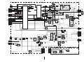
SECTION 5
DIAGRAMS
5-1. BLOCK DIAGRAMS
SIGNAL-IN
14
4
9
13
3
8
12
2
7
11
1
BGND
BLUE
GGND
GREEN
RGND
RED
GND
VD
HD
1
2
3
4
5
6
7
8
9
5
17
3
1
7
B IN
B OUT
G IN
G OUT
R IN
R OUT
11
19
8
21
5
1
SYNC
G IN
2
3
INV
Q007
6
CN310
NC
DOCSCL
DOCSDA
HDSTGND
16
1
2
3
4
13
14
12
C SYNC CLAMP
TO
D BOARD B
CN903
CN309
HSYNC
GND
VSOUT
CSYNC
BPCLP
SHARP
CBLK
TESTSW
A LEVEL
G IN
G OUT
R IN
R OUT
11
20
9
23
8
28
R OSD
R DRV
G OSD
G DRV
B OSD
B DRV
25
BRT
BLK
CONT
CLP
OSD BLK
13
7
8
10
5
INV.
Q004
R OSD OSD BLK
B OUT
G IN
G OUT
R IN
R OUT
TO FBT FOCUS
9
1
5
CRT
H G2
2
CN302
IC009
BLK SW/INVERTER
2
1
1Y
1A
3
1B
15
4
5
6
12
G OSD
B OSD
4B
4A
4Y
2A
2Y
CN304
1
2
CN314
1.2V
3
1
2
3
4
5
6
7
8
9
10
11
12
13
14
1
2
CN314
MIC OUT
GND
5
4
3
2
1
CN315
MIC OUT
GND
L IN
GND
R IN
SCL
VFLB
HFLB
RESET
G2
1
2
3
5
6
19
R IN
R OUT
G IN
B IN
G OUT
B OUT
CN305
1
+15V
2
NC
3 STBY+5VSW
4
+80V
5
GND
6
HI
7
+12V
8
GND
9 STBY+5V
GND
10
11
-15V
9
8
7
+VCC
+VCC SW
Q005,006
+IN
-IN
7
OUT
SPOT KILLER
Q001
D014
R
+12V
+150V
SHARP1
A LEVEL
J
G
+12V SW
Q009
D015
B
SW
Q010
B
G
R
CN5200
R IN
E
L IN
1
2
3
6
L,R BUFF
Q5201,5202
IC5200
E-VOL/TONE CONT
16
R IN R OUT
11
L OUT
L IN
17
IC5201
POWER AMP
IC5202
BUFFER
3
5
+IN1 OUT1
+IN2 OUT2
1
1
7
5
R IN
R OUT
L IN
L OUT
MUTE
Q5215,5216
D
SDA
SCL
DG
TO
D BOARD
CN502
IC805(2/2)
BUFF
7
IC804
14
13
12
11
10
9
8
7
6
5
4
3
2
1
R.G.BUFF
Q801,803,805
13
9
10
11
CN312
3
13
RO IN
GND
12
11
GO IN
10
GND
9
12V
8
BO IN
7 BLK OUT
SDA
6
SCL
5
-5V
4
3 SUB CONT
CONT
2
1 TEST SW
2
+IN 1
MUTE SW
Q5001
OUT 1
24
X800
24.5MHz
1
1
OUT1
+IN1
14
OUT3
+IN3
B IN
CLK DSC
OUT
BLK OUT
SDA
SCL
H SYNC
V SYNC
IGPE OUT
X
X1
X0
Y1
Y
Y0
13
12
2
CN5202
MUTE
R OUT
R GND
L OUT
L GND
12
8
OUT4
+IN4
8
IC5204 (2/2)
POWER
5
6
+IN 2
OUT 2
7
J5401
-IN 2
IC5601
+9V REG
+9V
O
I
POPING SOUND
PREVENTION
Q5401
POWER SW
Q5207
+16V SW
Q5206
1
2
3
4
5
13
12
11
10
9
8
7
6
5
4
3
2
1
B BUFF
Q808
4
20
21
6
5
CN801
RO IN
GND
GO IN
GND
+12V
BO IN
BLK OUT
SDA
SCL
-5V
A LEVEL2
A LEVEL
TEST SW
SW
Q809
15
11
A
10
B
9
C
GPE )
5-2
CN5061
AUDIO 16V
AUDIO 16V
AUDIO GND
AUDIO GND
AUDIO GND
CN5606
GND
CN5607
1
GND
1
B–SS3445<U/C>–B/D–P1–15
10
TO
E D BOARD
CN904
+16V
REF V
AA (VIDEO
5-1
1
2
3
4
5
POPING SOUND
PREVENTION
Q5205
R BUFF
Q806
3
G BUFF
Q807
IGPE IN
2
5
R IN
IC807 SWITCH
14
+IN2
-IN1
CLK DSC
IN
2
1
OUT2
10
1
-IN 1
IC805(1/2)
AMP&BUFF
COMP REF
G IN
CN5605
GND
CN5204
8 BB SW1
7
L NC
6 IIC DATA
5 IIC CLK
4
GND
3
MUTE
2
A-GND
1 POWER SW
19
20
18
IC5204 (1/2)
POWER
+9V
+16V
DC
SHIFT
Q810
1
U (AUDIO)
AUDIO IN/
MIC OUT
PIG-TAIL
+16V
CN800
GND
R IN
GND
G IN
GND
B IN
+5V
IGPE-A
CBLK
SHARP2
SHARP
IGPE-S
HS
VS
CN6001
GND
(HEADPHONE JACK)
MUTE
Q5402
+5V
1
MIC
CN316
1
R IN
2
GND
3
L IN
IC004
RGB CUT OFF CONTROL
7
SUB CONT
14
CONT
9
8
TO
C D BOARD
CN510
2B
IC005
CUT OFF/BRT CONT
1
CN6002
MUTE
R OUT
R GND
L OUT
L GND
4
MIC VCC
Q008
17
BD OUT
16
GD OUT
15
RD OUT
18
BRT
4
R C/O
5
G C/O
6
B C/O
1
2
3
4
5
TO
D BOARD
CN512
13
SDA
SDA
SCL
L,R MUTE
Q6001,6002
J6002
HEAD-PHONE
HV
(TO FBT)
10
26
IC008
9
8
7
6
5
4
3
2
1
1
2
3
4
KG
7 KR
5
R-SP
E
L-SP
E
SPEAKER
(L)
KB
8
27
STBY +5V
CN313
VS
HS
IGPE-S
SHARP
SHARP2
CBLK
IGPE-A
+5V
B IN
GND
G IN
GND
R IN
GND
B IN
3
11
14
SPEAKER
(R)
J001
18
IC003 OSD
15
TO
D BOARD A
CN902
B OUT
12
LEVEL
10
9
8
7
6
5
4
3
2
1
B IN
13
CN306
DDSCL
DDSDA
HOSTGND
IICSDA
GND
IICSCL
GND
HRTRC
VRTRC
HD
IC002
RGB OUT
IC001
RGB PRE-AMP
IC006
CN307
R
10
(VIDEO)
B
G
15
5
A
R
G
B
D-SUB15
PIG-TAIL
TO
F D BOARD
CN607
TO
D BOARD
HEAT SINK
T505 HST
T503
DFT
9
44
FUNCTION
SW
B
TO
A BOARD
CN309
CN903
HSYNC
GND
VSYNC
CSYNC
BPCLAMP
SHRPI
CBLANK
TEST SW
A LEVEL
9
8
7
6
5
4
3
2
1
45
4
2
30
20
28
22
46
21
6
SDA
WC
7
49
TO
U BOARD
CN5204
13
6
IC904
RESET
+5V-2
1
A
TO
A BOARD
CN306
10
9
8
7
6
5
4
3
2
1
CN901
TXD
RXD
+5V
D GND
4
3
2
1
4
LED GREEN
47
V DF
SDA
12
BUFF
Q505
DF AMP
Q504
1
10
5
9
23
S-CAP
CHANGE
Q512,515,516
SCL
LED DRIVE
Q901,902
OUT
IN
3
54
34
35
33
2
—
+
20
—
+
—
+
19
—
+
4
7
18
AMP
X902
VSI1
CS1
CLP
DA0
CBLK
VSI2
THERMAL
1
17
29
8
XS
H OUT
TH501
AMP
Q903
17
T504 HDT
H DRIVE
OUT
Q511
H DRIVE
Q501,502
4
1
D522
14
D523
12
1
2
3
4
5
6
H OUT
Q507
6
L503
H CENT
8
5
PA4
CN501
H DY+
H DY+
H DYH DYV DYV DY+
2
H.DY
V.DY
IC401 VOUT
SDA
SCL
H FB
32
14
H FLY
V SAW
V AGC
MUTE
26
REMOTE
ON/OFF
28
V DSC
LOCK
PD3
VSO
HSO
5
7
4
-IN
OUT
+IN
FB
2
7
HV REG
OUT
Q510
6
1
V IN
LOCK
DDCSCL
DDCSDA
HOST GND
8
H IN
RESET
S1-S3
INV
Q509
2
CHOPPER
Q503
DET
Q522,523
4
5
50-52
IC503
H CENT DRIVE
4
H CENT
Q506
2
H CENT
Q518
1
-IN
OUT
+B
+IN
9
HV
CN510
1.2KV
FV
TO
C A BOARD
CN301
TO CRT
ANODE CAP
RV501
HV
ADJ
14
13
19
-B
TDO
RDI
2
+RECT
H BLK
Q508
H CENT
1
T501 FBT
1
23
H CENT SW
39
38
22
13
8
HSI1
V FB
25
26
27
BUFF
24
3
Q520
37
36
6
5
4
3
2
1
CN902
DDCSCL
DDCSDA
HOST GND
IIC DATA
GND
IIC CLK
GND
HRTRC
VRTRC
H-USYNC
3
SCL
CN904
IIC DATA
IIC CLK
GND
MUTE
GND
POWER SW
LED RED
OSC IN
48
BUFF
BUFF
Q521
IC905 EEPROM
5
E
DA1
KEY IN
OSC OUT
5
11
LED DRIVE
Q904
D912
X901
24MHz
IC900
H SYNC BUFF
D938
2
2
12
+
—
15
3
IC501 PWM CONTROL
IC902
IC901 CPU
1
FOCUS
TO A BOARD
17
16
4
5
11
3
6
H CENT SW
Q517
D515
RECT
5
ABL
HV
16
4
D517
18
8
IC602 -12VREG
3
7
24
OUT
IN
IC502
ROTATION DRIVE
DEGAUSS
HEATER
REF V
3
ROTATION
1
2
+IN
-IN
OUT
-RECT
CN503
1 RATATION+
2 RATATION-
REMOTE ON/OFF
T602
PIT
7
D650
8 D651
T603
PRT
F601
2
LF601
LFT
1
D601
AC RECT
S601
T601
1
AC IN
3
5
D603
C1
4
7
4
REG
B1
3
SOFT START
Q654
D611
D605
E2
2
1
B2
4
D606
+150V
+80V
D654
9
D655
4
11
D656
12
13
1
14
VCC SW CONT
4
1
RELAY DRIVE
Q670
3
RY601
1
+15V DCP
Q603-605
D609
REG
Q607
Q608
1
2
3
4
5
6
7
8
9
10
11
HEATER SW
IC612
CN607
1 AUDIO VCC
2 AUDIO VCC
3
GND
GND
4
GND
5
I
O
+5V
3
+5V-2
+15V
+B DCP
Q671-673
2
IC605
BOOST
SWITCHING
Q602
D
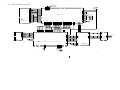
POWER,DEFLECTION
MICRO-CONTROLLER
CN1600
LATCH OUT 10
9
LATCH
8
OVP
AC SEN 7
6
V SEN
5
VCC
4
I SEN
3
DRV
2
P GND
1
S GND
D1605
1
CONTROLLER
2
IC1601
8
5
LATCH
Q1604-1606
Q1603
3
REG
IC1603
1
D1604
DA (POWER CONTROL)
B–SS3445<U/C>–B/D–P2–15
5-3
TO
D A BOARD
CN305
2
D671
CN602
10 LATCH OUT
9
LATCH
8
OVP
7 AC SEN
6
V SEN
5
VCC
4
I SEN
3
DRV
2
P GND
1
S GND
CN502
150V
NC
+B SW
+80V
GND
H1
+12V
GND
+5V
GND
-5V
-15V
1
IC603
+5V REG
+12V
+12V
5
VCC SW
Q601
TH602
+80V
+12V
-15V SW
Q606
D657
P GND
1
2
3
+150V
+5V-2
12V REG
IC604
D658
2
+15V
D653
10
ROTATION
SW
Q609
D652
5
1
SW
Q611
+15V SW
Q610
6
D604
Q608
L602
DGC
8
2
E1
C2
CN603
DGC2
NC
DGC1
1
MAIN SWITHCING
TH601
CN605
THP601A
THP601
IC611
9
4
REMOTE ON/OFF
CN600
12
2
5-4
TO
F U BOARD
CN5601
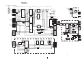
5-3. CIRCUIT BOARDS LOCATION
Part replaced ( [ )
HV ADJ
5-2. FRAME SCHEMATIC DIAGRAM
AUDIO IN/
MIC OUT
PIG-TAIL
Part replaced ( ] )
1 TEST SW
2 A LEVEL
3 A LEVEL2
-5V
4
SCL
5
SDA
6
7 BLK OUT
BO IN
8
12V
9
GND
10
GO IN
11
GND
12
ROIN
13
TEST SW
CONT
SUB CONT
-5V
SCL
SDA
BLK OUT
BO IN
12V
GND
GO IN
GND
ROIN
1
2
3
4
5
6
7
8
9
10
11
12
13
MIC OUT
GND
L IN
GND
R IN
5
4
3
2
1
CN801
13P
HV
(TO FBT)
CN302
1P
:TUB
4
3
CN310
4P
2
WHT
:S-MICRO 1
CN307
9P
WHT
:S-MICRO
CN313
14P
D
J (Stand block)
CN316
3P
WHT
:S-MICRO
1
2
3
4
5
6
7
8
9
CN314
1
2P
WHT
:S-MICRO 2
DA
5-4. SCHEMATIC DIAGRAMS AND PRINTED
WIRING BOARDS
MIC OUT
GND
Note:
R IN
E
L IN
1
2
3
-15V
GND
+5V
GND
+12V
H1
GND
+80V
+B SW
NC
150V
11
10
9
8
7
6
5
4
3
2
1
1.2KV
DDCSCL
DDCSDA
HOST GND
IICDATA
GND
IICCLK
GND
HRTRC
VRTRC
H-USYNC
10
9
8
7
6
5
4
3
2
1
1
A LEVEL
TEST SW
CBLANK
SHRP1
BPCLAMP
CSYNC
VSYNC
GND
HSYNC
1
2
3
4
5
6
7
8
9
CN502
11P
WHT
:S-MICRO
CN510
1P
CN5200
3P
WHT
:S-MICRO
CN5605
1P
1
GND
GND 1
CN6001
1P
CN512
1P
:TUB
CN602
10P
CN607
5P
WHT
:S-MICRO
CN904
6P
WHT
:S-MICRO
CN603
3P
MINI
(POWER CONTROL)
D
1
2
3
4
5
1
2
3
4
5
6
AUDIO VCC
AUDIO VCC
GND
GND
GND
POWER SW
GND
MUTE
GND
IIC CLK
IIC DATA
AUDIO
AUDIO
AUDIO
AUDIO
AUDIO
16V
16V
GND
GND
GND
POWER SW
A-GND
MUTE
GND
IIC CLK
IIC DATA
1
2
3
4
5
1
2
3
4
5
6
(POWER,DEFLECTION,MICRO-CONTROLLER)
GND
1
CN5601
5P
WHT
:S-MICRO
CN5202
5P
WHT
:S-MICRO
1
2
3
4
5
MUTE
R OUT
R GND
L OUT
L GND
MUTE
R OUT
R GND
L OUT
L GND
CN5606
1P
5-5
1
CN5607
1P
U(AUDIO)
1
2
3
4
5
6
GND
B-SS3445<U/C>-KESSENZU
IC603, IC901, D515
D517, C540, C542
C544, R543, R547
R549, R552, T501 (FBT)
Beam Current
Protector Circuit
Check
D Board
IC603, IC604, IC901
C535, C541, R515
R545, R546, R548
R550, R934, T501 (FBT)
1
2
3
CN6003 4
4P
RED
:S-MICRO
R-SP
E
L-SP
E
SPEAKER
(R)
SPEAKER
(L)
Device
1
3
*
Printed symbol
Circuit
Terminal name
Collector
Transistor
Base
Transistor
Base
Diode
Emitter
Collector
Emitter
Cathode
Anode
Cathode
4
Diode
Anode
(NC)
Cathode
5
• All resistors are in ohms.
• f : nonflammable resistor.
• F : fusible resistor.
¢ : internal component.
•
• p : panel designation, and adjustment for repair.
• All variable and adjustable resistors have characteristic curve B,
unless otherwise noted.
e : earth-ground.
•
•
E : earth-chassis.
• All voltages are in V.
• Readings are taken with a 10 M digital multimeter.
• Readings are taken with a color-bar signal input.
• Voltage variations may be noted due to normal production
tolerances.
•
* : Can not be measured.
• Circled numbers are waveform references.
• s : B + bus.
• S : B – bus.
• The components identified by [ in this basic schematic diagram
have been carefully factory-selected for each set in order to
satisfy regulations regarding X-ray radiation.
Should replacement be required, replace only with the value
originally used.
• When replacing components identified by ] , make the
necessary adjustments indicated. (See page 3-1)
• When replacing the part in below table, be sure to perform the
related adjustment.
Diode
Anode
(NC)
Common
6
7
8
9
0
!¡
Diode
Anode
Diode
Cathode
Common
Anode
Cathode
Common
Diode
Anode
Anode
Common
Diode
Anode
Anode
Common
Diode
Cathode
Cathode
Common
Diode
!™
Diode
!£
Transistor
(FET)
Cathode
Anode
Anode
Cathode
Drain
Cathode
Cathode
Anode
Anode
Source
Gate
D
Source
Gate
!¢
Transistor
(FET)
!∞
Transistor
(FET)
Source
Drain
Gate
Transistor
Emitter
Collector
Base
!§
–
Drain
G
S
S
D
D
G
G
S
S
Discrete semiconductot
Ver.1.5
Note: Les composants identifiés per un tramé et une
marque ! sont critiques pour la sécurité. Ne les
remplacer que par une pièce portant le numéro
spécifié.
Note: The components identified by shading and mark
! are critical for safety. Replace only with part
number specified.
5-6
D
G
(Chip semiconductors that are not actually used are included.)
V.DY
ROTATION
ROTATION+ 1
ROTATION- 2
CN503
2P
CN6002
5P
WHT
:S-MICRO
(HEADPHONE JACK)
D HEAT SINK
CN501
6P
:DY
1
2
3
4
5
J
CN5204
6P
WHT
:S-MICRO
DY+
DY+
DYDYDYDY+
DGC1 3
NC 2
DGC2 1
CN902
10P
WHT
:S-MICRO
CN903
9P
WHT
:S-MICRO
D Board
2
• All capacitors are in µF unless otherwise noted. (pF: µµF)
Capacitors without voltage indication are all 50 V.
• Indication of resistance, which does not have one for rating
electrical power, is as follows.
H
H
H
H
V
V
DA
DEGAUSSING
COIL
10
9
8
7
6
5
4
3
2
1
H.DY
CN1600
10P
LATCH OUT
LATCH
0VP
AC SEN
V SEN
VCC
I SEN
DRV
P GND
S GND
HV Hold-down
Circuit Check
Terminal name of semiconductors in silk screen
printed circuit ( )
Pitch: 5 mm
Rating electrical power 1/4 W (CHIP : 1/10 W)
10 LATCH OUT
9 LATCH
8 0VP
7 AC SEN
6 V SEN
5 VCC
4 I SEN
3 DRV
2 P GND
1 S GND
IC501, C553, C554
C555, C558, C561
R540, R564, R567
RV501, T501 (FBT)
U (Stand block)
BGND
BLUE
GGND
GREEN
RGND
RED
GND
VD
HD
1
2
3
CN301
2P
2
1
CN305
11P
:S-MICRO
D-SUB 15
(PIG TAIL)
R IN
GND
L IN
VSOUT
CSYNC
BPCLP
SHARP
CBLK
TEST SW
A LEVEL
GND
HSYNC
CN306
10P
WHT
:S-MICRO
1.2KV
CN309
9P
WHT
:S-MICRO
9
8
7
6
5
4
3
2
1
(VIDEO<GPE>)
HOSTGND
DDCSDA
DDCSCL
NC
CN308
1P
:TUB
11
-15V
10
GND
9
STBY+5V
8
GND
7
+12V
6
H1
5
GND
4
+80V
STBY+5V SW 3
2
NC
1
+150
AA
1
2
3
4
5
6
7
8
9
10
11
12
13
14
DDCSCL 10
DDCSDA 9
HOSTGND 8
IICSDA 7
6
GND
IICSCL 5
4
GND
HRTRC 3
VRTRC 2
HD
1
CN800
14P
VS
HS
IGPE-S
SHARP
SHARP2
CBLK
IGPE-A
+5V
B IN
GND
G IN
GND
R IN
GND
VS
HS
IGPE-S
SHARP
SHARP2
CBLK
IGPE-A
+5V
B IN
GND
G IN
GND
R IN
GND
D Board
AA
CN304
1P
:TUB
CN312
13P
HV Regulator
Circuit Check
A
CRT
CN315
5P
WHT
:S-MICRO
A(VIDEO)
1
2
3
4
5
6
7
8
9
10
11
12
13
14
RV501
5-7
(a)
— A BOARD (Conductor Side) —
1
2
3
VIDEO
— A BOARD (Component Side) —
• A BOARD
SEMICONDUCTOR
LOCATION
4
1
2
3
4
IC
(
IC001
IC002
IC003
IC004
IC005
IC006
IC008
IC009
A
Conductor
Side
) (Component
Side )
B–2
A–3
A–2
B–4
B–4
B–2
A–1
B–1
B–3
A–2
A–4
B–1
A
B–3
TRANSISTOR
Component
( Conductor
Side ) ( Side )
Q001
Q004
Q005
Q006
Q007
Q008
Q009
Q010
C–4
A–1
A–2
A–2
B–1
B–1
B–4
B–4
C–1
*
–
1
2
1
1
1
1
1
B
B
DIODE
Component
( Conductor
Side ) ( Side )
D001
D003
D005
D006
D007
D008
D009
D013
D014
D015
D101
D104
D105
D106
D201
D204
D205
D206
D301
D304
D305
D306
C
C–2
C–1
B–1
A–1
B–1
B–1
B–1
C–1
B–4
B–4
B–2
A–4
A–4
B–3
B–2
A–4
A–4
B–3
B–1
A–4
A–4
B–3
C–3
C–4
B–4
A–4
B–4
B–4
B–1
A–1
A–1
B–2
A–1
A–1
B–2
A–1
A–1
B–2
*–
–
–
–
–
–
3
3
–
3
6
–
–
–
6
–
–
–
6
–
–
–
*: Refer to Terminal name of
C
NOTE:
The circuit indicated as left contains high voltage of over
600 Vp-p. Care must be paid to prevent an electric shock in
inspection or repairing.
semiconductors in silk screen
printed circuit (see page 5-7)
5-8
5-9
5-10
(1) Schematic Diagram of A Board
7
8
9
10
11
12
J001
D301
1SS226
B_IN
2.6
VBIAS
G_IN
2.5
R_IN
2.7
GND3
VCC
R_OUT
55.0
GND2
G_OUT
57.0
GND1
B_OUT
56.4
9
6
5
3
1
10
8
7
4
2
9 G2
G2
7
8
4
5
R351
100
1/2W
:RC
2
3
4
5
6
R133
470
GT103
R309
1M
:CHIP
FB310
1.1
R209
1M
:CHIP
FB210
1.1
R109
1M
:CHIP
7
FB110
1.1
8
R151
100
1/2W
:RC
9
L101
1.2µH
GT104
CN302
1P
:TUB
CN310
4P
WHT
:S-MICRO
R017
100 :CHIP C050
0.1
25V
B:CHIP
4
3
2
1
C084
0.1
25V
B:CHIP
11
R014
100
:CHIP
R306
10k
:CHIP
R216
15k
:CHIP
C092
0.1
25V
B:CHIP
R208
4.7k
:CHIP
R307
4.7k
:CHIP
C105
0.1
25V
C205 B:CHIP
0.1
25V
C305
0.1 B:CHIP
25V
B:CHIP
C022
47
25V
5
6
Q001
2SC5022
SPOT KILLER
11.5
10.9 R031
R049
100k
:CHIP
1k
:CHIP
4.5
+
GND
4.5
10.7
OUT
VCC
C027
0.01
B:CHIP
STBY+5V
R047
10k
:CHIP
C036
0.1
25V
B:CHIP
R046
100k
:CHIP
Q005
2SB798T1DLDK
IC008
M62392FP
3.8
R035
0
:CHIP
Q004
2SC2412K
BUFF
R034
0 :CHIP
D008
RD5.6ES-TIB2
C085
0.1
25V
B:CHIP
2.5
R068
10k
:CHIP
R069
15k
:CHIP
STBY +5V
FB012 0 :CHIP
3.0
C004
47
25V
C067 0.01 B:CHIP
R313
100
:CHIP
C068 0.01 B:CHIP
6
D005
1SS119-25TD
R057
1k
:CHIP
R062
470 :CHIP
C069 0.01 B:CHIP
7
Q008 2SD601A
FB013 0 :CHIP
FB014 0 :CHIP
D006
1SS119-25TD
FB015 0 :CHIP
D007
RD5.6ES-TIB2
CN316
3P
WHT
:S-MICRO
TO U BOARD
CN5200
D013 D009
MA111 MA111
CN314
2P
WHT
:S-MICRO
R314
1k
:FPRD
C060
22
5
4
R063
0
:CHIP
C070
0.01
B:CHIP
FB016 0 :CHIP
C079
0.1
25V
B:CHIP
C071 C072
0.01 0.01
B:CHIP B:CHIP
C065
47
25V
4.2
C073 0.01 B:CHIP
1
0.3
2
R052
10k
:CHIP
R036
100
:FPRD
3
R006
100
:CHIP
FB009 R020
JW(5) 100
:CHIP
C066
0.01
B:CHIP
RESET CS0
4.9
SCL
CS1
4.5
SDA
CS2
4.6
R C/O VDD
0
G C/O VCC
3.8
3.2
B C/O
G2
3.2
3.2
SUBCONT BRT
1.8
3.2
A LEVEL BD OUT
1.7
2.9
SHARP1 GD OUT
0
3.2
V LOW RD OUT
1.7
VREF1 CONT
GND VREF2
C074 0.01 B:CHIP
C075 0.01 B:CHIP
C076 0.01 B:CHIP
C077 0.01 B:CHIP
+80V
+12V
C016
47
25V
5V
FB011
1.1
• A BOARD WAVEFORMS
CN308
1P
:TUB
+12V
C017
47
25V
CN304
1P
:TUB
C055
1000p
500V
B
R072
220k
:CHIP
Q009
DTA124EKA
D015
UDZ-TE-17-6.2B
Q010
2SC2412K
R075
10k
:CHIP
R073
220k
:CHIP
R059
1k
:CHIP
Q006
R074
27k 2SC2412K
:CHIP
R058
1k
:CHIP
11
-15V
GND
10
9 STBY+5V
L006
GND
8
100µH
+12V
7
H1
6
C001
1000p 5
GND
500V
B
4
+80V
C002
3 STBY+5V SW
0.01
:PET
2
NC
+150
1
TO D BOARD
CN502
0.7 Vp-p (H)
3
G
0.7 Vp-p (H)
4
H
0.7 Vp-p (H)
5
0.7 Vp-p (H)
6
H
0.1
0.7
0.7 V p-p (H)
H
R060
10k
:CHIP
7
R061
4.7k
:CHIP
0.7 Vp-p (H)
8
C078 0.01 B:CHIP
B-SS3445<U/C>-A..
50.0 Vp-p (H)
9
I
50.0 Vp-p (H)
CN315
5P
WHT
:S-MICRO
!¡
50.0 Vp-p (H)
0
50.0 Vp-p (H)
!™
J
50.0 Vp-p (H)
Schematic diagram
5-11
2
CN305
11P
:S-MICRO
AUDIO IN/
MIC OUT
PIG-TAIL
J
1
F
C056
0.01
100V
:PET
L004
JW(5)
STBY+5V
R051
1k
:CHIP
723.0 22M
:RN
R045
2.2k
:CHIP
C028
47
25V
R308
4.7k
:CHIP
R316
15k
:CHIP
R053
IC005
NJM4558M
CUT OFF/BRT CONT
C029
0.1
25V
B:CHIP
7
R108
4.7k
:CHIP
R040
470k
:CHIP
8
R110
220k
D014
1SS119-25TD
16
15
14
13
R206
10k
:CHIP
R021
FB010 100
JW(5) :CHIP
10
9
8
7
6
5
4
3
2
1
R310
220k
R029
82k
:CHIP
R210
220k
R207
4.7k
:CHIP
10
INT
R116
15k
:CHIP
9
4.6
SCL VDD
R056
0 :CHIP
R018
100 :CHIP
R024
4.7k
:CHIP
R106
10k
:CHIP
R303
0 :CHIP
12
1
2
3
4
5
R203
0 :CHIP
13 14 15 16 17 18 19 20 21 22 23 24
I
HOSTGND
DDCSDA
DDCSCL
NC
6
FB007 JW(5)
SS
0
4.6
SDA VFLB
R055
0 :CHIP
R022
0
:CHIP
R032
C053
3.9k
0.1
:RN CHIP 25V
B:CHIP
E
CN303
1P
:TUB
R033
15k
:RN CHIP
C054
0.1
250V
:MPS
R107
4.7k
:CHIP
L002
470µH
7
Q007
2SC3735
0
3.8
HFLB OSD_BLK
R103
0
:CHIP
R071
10k
:CHIP
8
H
TO D BOARD
CN902
C047
47
25V
0.7
9
8
7
6
5
4
3
2
1
CN306
10P
WHT
:S-MICRO
DDCSCL
DDCSDA
HOSTGND
IICSDA
GND
IICSCL
GND
HRTRC
VRTRC
HD
R025
4.7k
:CHIP
EMI
0
VCO R_OSD
1.7
0
RP G_OSD
1.7
0
VDDA B_OSD
R070
15k
:CHIP
12 11 10 9
G
FL001
VSS
C018
10
200V
5
4
3
2
1
TO D BOARD
CN903
R067
100
:CHIP
MIC OUT
GND
L IN
GND
R IN
GND
VSOUT
CSYNC
BPCLP
SHARP
CBLK
TEST SW
A LEVEL
0.3
1
2
HSYNC
R023
0
:CHIP
VSSA
0.4
8
CN309
9P
WHT
:S-MICRO
C042
C043
0.1
47p
25V
:CHIP
B:CHIP
R004
C044
R003
1.8k
68000p 5.6k
:CHIP
B:CHIP :CHIP
C046
C045
R005
0.01
470k
47p
B:CHIP :CHIP
:CHIP
STBY +5V
R065
2.2k
:CHIP
MIC OUT
GND
F
R002
1.5k
:CHIP
1
2
3
TO AA BOARD
CN800
D
140V
IC003
LSC4514P2
OSD
R IN
GND
L IN
E
GT101
L201
1.2µH
D105
HSS82
1
1
2
3
4
5
6
7
8
9
10
11
12
13
14
C
R251
100
1/2W
:RC
+12V
VS
HS
IGPE-S
SHARP
A LEVEL
CBLK
IGPE-A
+5V
B IN
GND
G IN
GND
R IN
GND
L003
22µH
L301
1.2µH
IC004
TDA6103Q RGB CUT OFF CONTROL
CN313
14P
B
1.2KV
TO D BOARD
CN510
GT102
IC009
SN74HC02ANS
BLK SW/INV
R030
0
:CHIP
FB003
JW(5)
SG201 SG101
+140V
17
16
R037
0
:CHIP
1
2
R048
2.2M
1W
:RN
FB001 1.1
0
LEVEL
R233
22
KR
5
FB005 1.1
GND
C304
0
:CHIP
R043
0
:CHIP
C206
0.1
250V
:MPS
D304
HSS82
C106
0.1
250V
:MPS
VIP
2.5
VCC
GND
0.1
CLAMP
C051
47
25V
D204
HSS82
D205
HSS82
R_IN
2.5
G_IN
2.5
B_IN
2.5
GND
C204
0
:CHIP
C049
0.01
B:CHIP
D104
HSS82
R333
22
TO D BOARD
CN512
CN301
2P
10
SG301
C306
0.1
250V
:MPS
KR
4
4
3.1
GND C SYNC
C037
220p
:CHIP
0
IY VCC
4.8 4.1
IA
4Y
0.1
IB
4B
2Y
4A
0
2A
3Y
0
2B
3B
GND 3A
11
7
TO D BOARD
T501(HV)
SG002
3
6
A
PICTURE
TUBE 15FRS
1
3 G1
4 H2
5 H
3
DEFF.
C080
47
16V
R064
SG001 10k
1/2W
:RC
80V
9 10 11 12 13 14
GND
C011
0.1 C014
100V 47
:PT 100V
C064
0.22
25V
B:CHIP
KB
8
7 KG
6
12
C035
470p
2kV
B
FB301
0
:CHIP
D305
HSS82
6
C019
47
25V
C094
0.1
25V
B:CHIP
FB201
0
:CHIP
C041
0.22
25V
B:CHIP
C012 C013
0.01 220
B:CHIP 16V
R215
390
4.8 :RN-CP
7
R007
1k :CHIP
2.4
R028
1.5k
:CHIP
FB101
0
:CHIP
R311
47
:FPRD
8
SYNC G IN
VCC2
2.7
6
B_OUT
C302
4.7
:BP
4.0
R211
47
:FPRD
11
10
9
17
V901
1
13
13
C089
0.1
25V
:CHIP
5
R041
2P
:CHIP
R027
10k
:CHIP
FB302
0
:CHIP
R315
390
:RN-CP
1
VCC
C303
2p
:CHIP
C093
0.1
25V
B:CHIP
FB202
0
:CHIP
2
19
B1_IN
15
VCC
GND
14
G_OUT
18
4
C061
0.1
25V
B:CHIP
C062
0.1
25V
B:CHIP
C063
0.1
25V
B:CHIP
R111
47
:FPRD
R204 R104
0
0
C015 :CHIP:CHIP
0.1
25V
B:CHIP
FB102
0
:CHIP
3
20
3
12
C087
0.1
25V
:CHIP
C090
0.1
25V C048
:CHIP 0.01
B:CHIP
2.3
C202
4.7
:BP
C010
0.1
25V
B:CHIP
C009
220
16V
15 16 17 18 19 20 21 22 23 24 25 26 27 28
1
2
3
4
21
GND
G1_IN
C203
2p
:CHIP
C102
4.7
:BP
6
5
R_OUT
GND
2.6
R312
33
:CHIP
2.4
14 13 12 11 10 9
GND
2
2.6
1
2
3
4
5
6
7
8
9
10
11
12
13
11
R304
0
:CHIP
STBY+5V
1
22
1
R1_IN
2
R212
33
:CHIP
D003
RD5.6ES-T1B2
R026
10k
:CHIP
2.6
C103
2p
:CHIP
D101
1SS226
3
R016
10k
:CHIP
R112
33
:CHIP
4
FL101
EMI
R101
75
:RN
5
R201
75
:RN
IC006
CXA8075S
6
FL201
EMI
D201
1SS226
7
D
C301
0.47
16V
B:CHIP
C201
0.47
16V
B:CHIP
C101
0.47
16V
B:CHIP
8
TO AA BOARD
CN801
0
3.3
R OSD R DRV
0
2.9
G OSD G DRV
0
3.2
B OSD B DRV
0
1.9
OSD BLK BRT
2.2
4.9
R IN R CLP
2.7
VCC1 R OUT
VCC2
GND
2.2
GND
G IN
2.5
VCC1 G OUT
4.9
GND G CLP
2.6
2.2
B IN B OUT
5.0
2.0
V REFB CLP
1.7
CONT
BLK
1.5
OSD CONT CLP
STBY +5V
EMI
R301
75
:RN
D001
RD5.6ES-T1B2
CN312
13P
TEST SW
CONT
SUB CONT
-5V
SCL
SDA
BLK OUT
BO IN
12V
GND
GO IN
GND
ROIN
FL301
9
1
2
3
4
5
6
7
8
9
12V
10
RCV
9
8
10
C
IC001
MM1382
RGB PRE-MIX
OSD MIX
11
BGND
BLUE
GGND
GREEN
RGND
RED
GND
VD
HD
B
R115
390
:RN-CP
8
16
12
G3
11
7
CN307
9P
WHT
:S-MICRO
15
14
IC002
LM2406T
RGB OUTPUT
A(VIDEO)
D-SUB 15
(PIG TAIL)
13
2
6
D306 HSS82
A
5
1
4
D206 HSS82
3
D106 HSS82
2
B_OUT
131.0
G_OUT
123.1
R_OUT
124.5
1
5-12
Ò (a) board
5-13
50.0 Vp-p (H)
(d)
POWER, DEFLECTION
MICRO-CONTROLLER
• D BOARD
SEMICONDUCTOR LOCATION
IC
IC401
IC501
IC502
IC503
IC602
IC603
IC604
IC605
IC611
IC612
IC900
IC901
IC904
IC905
B-4
A-6
C-6
B-3
B-5
C-5
C-4
D-3
E-6
D-6
D-6
C-6
B-7
B-6
TRANSISTOR
Q501
Q502
Q503
Q504
Q505
Q506
Q507
Q508
Q509
Q510
Q511
Q512
Q515
Q516
Q517
Q518
Q520
Q521
Q522
Q523
Q601
Q602
Q603
Q604
Q605
Q606
Q607
Q608
Q609
Q610
Q611
Q670
Q671
Q672
Q673
Q901
Q902
Q903
Q904
Q905
A-6
A-6
C-1
A-1
A-6
C-6
B-3
C-3
A-6
C-1
A-4
B-5
B-5
B-5
B-5
B-5
C-3
B-5
A-6
A-6
E-3
E-3
D-5
D-5
D-5
C-6
E-4
E-3
C-6
C-6
C-5
C-3
C-4
C-4
C-4
E-7
E-7
B-6
B-7
B-6
*
1
1
–
–
–
–
–
–
1
–
–
–
–
–
–
–
–
–
1
1
–
–
1
1
1
–
–
–
1
–
1
–
–
1
1
1
1
1
1
1
DIODE
NOTE:
The circuit indicated as left contains high voltage of over
600 Vp-p. Care must be paid to prevent an electric shock in
inspection or repairing.
D401
D402
D403
D404
D405
D501
D502
D503
D504
D506
D507
D508
D509
D510
D511
D512
D513
D514
D515
D516
D517
C-4
C-4
B-5
C-4
C-5
A-4
B-3
B-5
C-2
C-3
C-4
A-6
C-1
C-2
B-2
B-3
C-1
A-3
A-1
C-2
A-1
*–
–
3
3
–
–
–
–
–
–
–
–
–
–
–
–
–
–
–
–
–
D518
D520
D521
D522
D523
D524
D525
D527
D550
D551
D601
D602
D603
D604
D605
D606
D607
D608
D609
D611
D612
D613
D614
D615
D618
D619
D621
D622
D623
D624
D650
D651
D652
D653
D654
D655
D656
D657
D658
D662
D670
D671
D901
D902
D903
D904
D905
D906
D907
D908
D909
D910
D911
D912
D914
D915
D916
D917
D918
D919
D920
D922
D924
D925
D928
D929
D932
D933
D934
D935
D936
D937
D938
D939
C-3
C-2
C-2
A-7
A-7
C-3
C-3
C-3
B-2
B-2
D-2
E-3
E-3
D-6
E-5
E-5
E-5
E-5
E-4
E-5
E-4
E-4
E-4
E-4
B-5
E-6
E-6
D-5
D-5
D-6
D-4
D-4
D-3
D-4
D-4
D-5
D-5
D-5
D-5
D-4
C-2
C-4
E-7
C-6
D-6
D-6
D-7
D-7
E-6
D-6
D-6
D-6
D-6
E-7
D-6
D-6
D-6
D-6
D-6
C-6
B-7
D-6
C-6
C-6
C-6
C-6
C-6
C-6
B-6
D-6
E-7
E-7
A-7
A-6
–
–
–
–
–
–
–
–
–
–
–
–
–
–
3
–
–
–
–
–
–
–
–
–
3
3
3
3
3
3
–
–
–
–
–
–
–
–
–
–
–
–
3
3
3
3
3
3
3
3
3
3
3
–
3
3
3
3
3
3
–
3
3
3
3
3
3
3
3
3
3
3
–
–
— D BOARD —
1
2
3
4
5
6
A
B
C
D
VARIABLE
RESISTOR
RV501
A-1
E
CRYSTAL
X901
X902
B-6
B-7
*: Refer to Terminal name of semiconductors
5-14
in silk screen printed circuit (see page 5-7)
5-15
5-16
7
(2) Schematic Diagram of D Board
1
2
3
4
5
6
7
8
9
10
11
12
13
15
14
16
17
18
19
20
21
5V
A
5V-2
5V-2
C929
0.001
B:CHIP
IIC CLK
IIC DATA
R940
2.7k
:RN-CP
RXD
TXD
5V
D905
MA111
5V-2
4.2
3.8
4.5
HSO
CSYNC
CSI
HSI1
VSS
2
3
C910
0.1
:PT
3 2
IC901
ST72751N9B1/LAM
CPU
5.3
Q902
2SC2412
LED DRIVE
5V
R927
0
:CHIP 4.9
H-SYNC
C943
100p
CH:CHIP
R948
100
:CHIP
29
0.6
R925
4.7k
:CHIP
B
TO A BOARD
CN306
C
7
8
4.9
R961
470
CN903
9P
WHT
:S-MICRO
R956
100
:CHIP 9
D903
MA111
C912
100
16V
1
8
7
6
5
4
3
2
1
R935
100 :CHIP
R938
100 :CHIP
R936
100P :CHIP
H FLY
5V-2 5V-2
5V-2
D904
MA111
D
TO U BOARD
CN5204
C911
0.01
:PT
R924
100
IC904
PST600C
RESET
POWER SW
GND
MUTE
GND
IIC CLK
IIC DATA
NC
BB SW1
CN904
8P
WHT
:S-MICRO
D621
UDZ-5.6B
A0
6
R921
100
:CHIP
IC905
M24C08-BN6
EEP ROM
A1
VCC
A2
WC
VSS
SCL
5
4.5
SDA
1
4.6
D902
UDZ-5.6B
22
21
20
19
18
17
16
Q901
2SC2412
LED DRIVE
ROTATION
DEGAUSS
25
24
23
REMOTE ON/OFF
30
29
27
26
5
6
7
8
9
10
11
12
13
14
15
2
C942
22
25V
Q905
UN2115-QRS
C909 C908
2200 0.01
10V B:CHIP
H BLK
30
H BLK
31
0.3 0.3
28
V.DF
VDD
0
H-USYNC
R598
1k
:CHIP
HFB
32
VSO
27
R504
0.47
:FPRD
Q501
2SC2412K
H DRIVE
0.5
PD3
26
E/W
PC1
0
25
V-USYNC
V SAW
HOST GND
3
R958
47
4.9
PD4
DDC CLK
4
R957
47
4.7 4.5
0
IIC CLK
DDC DATA
33
ITA DDCSCL
SCL
4.6
0
R905
100
:CHIP
D912
SPB-26MVWF
RXD
34
CLP DDCSDA
1
2
3
4
5
6
7
8
R902
100
D619 :CHIP
UDZ-5.6B
IIC DATA
35
4.4
R928
100
:CHIP
DDCSCL
DDCSDA
HOST GND
IICDATA
GND
IICCLK
GND
HRTRC
VRTRC
H-USYNC
R901
100
CBLANK
C925
0.01
B:CHIP
F
SDA
0
D928
UDZ-5.6B
R911
470
:CHIP
R959
10k
:CHIP
36
HEATER
RDI
4.1 4.6
VSI2
24
E
LOCK
-0.4 4.8
VSI1
R910
330
:CHIP
TXD
37
L902 R933
JW(5) 1.5k
:CHIP
TDO
FB901
5MM
D908
MA111
R918
1k
:CHIP
5V-2
38
VCC
Q903
2SC2412
AMP
5.3
3.2 4.9
VFB
D907
MA111
0.3
FB903
0.45UH
39
D924
MA111
C917
0.0068
:CHIP
C926
1000
16V
NC
R914
100
:CHIP
D909
UDZ-5.6B
40
V FLY
V-SYNC
41
PB1
3.0
23
H.OUT
3
H.GND
D919
UDZ-5.6B HV
D925
MA111
NC
4.2
22
H.FLY
PB2
21
0.4
0.5
C927
0.01
B:CHIP
C924
22
C921
470
16V
C920
0.01
B:CHIP
42
5.4
PB3
C915
22p
CH:CHIP
43
AFC2
12V
ABL
C914
22p
CH:CHIP
11
0
R920
1k
:CHIP
CBLANK
NC
4.9
THERMAL
LED GREEN
X901
24MHz
0
PB4
C922
1.0
D939
RB441Q
2.3
20
H.DF
C916
22
PB5 CLKOUT
0
19
9V
9.6
0
PB6 OSCOUT
18
V.DF
R931
2.2k
:RN-CP
C918
10
9.6
6.6
PB7 OSCIN
17
H.AGC
DELAY CAP
R.F/V
D918
UDZ-5.6B
2.1
16
C913
0.1
:PT
1.6
R929
4.7k
:CHIP
C928
0.01
B:CHIP
PA6
4.3
15
D
4.9
V.SIN
R934
10k
:CHIP
R926
0
:CHIP
VDD2 CBLK
S3
D929
UDZ-5.6B
LED RED
44
C923
470p
CH:CHIP
C919
1
MUTE
R922
10k
:CHIP DDC 5VDET
VSS2
R953
10k
:CHIP
R954
10k
:CHIP
45
10.2
VCO.FI
C930
0.01
:PT
PA5
4.5
46
E/W
R947
6.8k
:CHIP
S907
0
DA8
IIC DATA
S2
D932
UDZ-5.6B
47
3.8
E/W
L901
100µH
V-REF
PA4
48
REF
V.SAW
4.9
V SAW
PA3
4.9
0
14
AFC1
V.AGC
DA7
13
5.0
DA6
0
C940
0.01
B:CHIP
12
5.7
D934
UDZ-5.6B
D933
UDZ-5.6B
49
4.2
V.OSC H.PH.FI
0.3
11
3.9
R946
2.7k
:RN-CP
RESET
H-USYNC
2
PA2
10
C906
1.0
:MPS
H.IN
V.GND
D920
RB441QT-77
R962
0
:CHIP
PA1
4.9
4.5
9
C905
0.068
:PP
GPE
S906
28
1
2
3
4
4.9
V.DIV
DA5
D910
UDZ-5.6B
S1
50
4.5
SCL
0.3
JW401
5MM
R945
1.5k
:RN-CP
R951
100
:CHIP
8
S905
X902
V-USYNC
7
VOLUME-
4.9
1
R930
100
:CHIP
R912
1k
R913
100
2.3
DA4
10
9
8
7
6
5
4
3
2
1
DDC CLK
PA0
51
0
V.IN
RESET
CN902
10P
WHT
:S-MICRO
R917
15k
:CHIP
2.1
52
4.6
DA3
A
FB902
1.1
R906
10k
:CHIP
R916
15k
:CHIP
D GND
+5V
RXD
TXD
CN901
4P
WHT
:S-MICRO
53
SDA
R944
1k
:RN-CP
S904
C
X5
R915
4.7k
:CHIP
R932
100
:CHIP
VOLUME+
0.4
DA2 RESET
6
C903
0.01
B:CHIP
4.7
LOCK
R939
270
:RN-CP
C938
100p
:CHIP
5
C902
470
16V
R943
680
:RN-CP
IR
4.9
54
MENU
S903
D.GND
D VCC
55
(POWER,DEFLECTION,MICRO-CONTROLLER)
DA1
LOCK
4
S911
TEST
3
CONT-
DA0
R904
1k
:CHIP
D901
MA111
R908
R909
820
820
:RN-CP :RN-CP
4.7
4.9
R907
100
1/2W
R941
470
:RN-CP
R942
470
:RN-CP
4.9
2
S910
D
B
IC902
CXA8071AP
D906
MA111
56
CONT+
1
Q904
2SC2412K
D938
SEL1922-C,D
IIC CLK
S901
H.CENT
BRANDED
1
2
3
4
R903
1k
:CHIP
KEY SCAN
22
D936
MA111
R937 C936
1k
100p
:CHIP CH:CHIP
A LEVEL
TEST SW
CBLANK
SHRP1
BPCLAMP
CSYNC
VSYNC
GND
HSYNC
E
TO A BOARD
CN309
V FLY
5.3
F
R952
3.3k
:CHIP
CSYNC
BPCLAMP
4
5.3
V-REF
Q502
2SA1037AK
H DRIVE
ABL
H CENT
ROTATION
C937
47p
CH:CHIP
HV
V-SYNC
0.3
C931
470p
:PT
D916
MA111
D914
MA111
H BLK
G
D604
1SS119
D607
1SS119
C675
100
16V
5
Q654
2SA1309A
SOFT START
D611
1SS119
C670
2.2
4
3
R679
10k
:CHIP
4.5
R678
470k
4.5
R677
0 150k
IC611
DM-58
SHNT REG
12V
R667 12.5
10k
0
R680
10k
:CHIP
R676
1k
:CHIP
Q671
2SA1091O
+B OCP
R681
10k
:CHIP
R662
470k
C672 Q672
47
25V 2SC2412
R513
Q511
220
IRFU110
2W
H DRIVE OUT :RS
D501-0.2
R508 RD12ES
C659 R661 R660
0.001 1k
12k
200V
:FPRD
:PT
10
9
8
7
6
R642
100
T601
515UH
3
R643
4.7k
:CHIP R644
22k
:CHIP
R509
22k
2
L509 5
HLC
C581
3300p
T505
500V
HST
B:CHIP
14.0
BOOST SWITCHING
C607
1
400V
:MPS
R604
10k
S
0
CN605
2P
:LAGE
1
R606
10
:FPRD
C613
220
450V
D602
1SS119
R610
0.22
3W
:RS
L602
22µH
THP601 1
THP601A 2
C614
0.01
630V
:MPS
8.7
1
C615
47
25V
R623
360k
:RN
R624
270k
:RN
R619
330k
:RN
R627
330k
:RN
R625
330k
:RN
R628
330k
:RN
R605
47k
2
0
TH601
5.1
300V
C604 C603
4700pF 4700pF
250V 250V
:E
:E
M
S601
C608
470p
250V
:B
C616
220
25V
R949
10k
:CHIP
4
1
3
2
R502
180k
:CHIP
IC605
PC123FY2
VCC SW CONT
R507
1.8k
:RN
Q505
2SA1309A
BUFF
6
6.3V
7
D521
RPG02-17PKG23
C503
0.01
150V
O
R586
2.2k
1/2W
R585
2.2k
1/2W
D527
RD5.1ES
4
5
THERMAL
R600
2.2k
R587
1k
:CHIP
6
H BLK
C516
100p
CH:CHIP
D507
RD5.1ES
116.2
1
C573
4.7
160V
0.5
C504
0.001
500V
B
C505
27p
2kV
:SL
3
R599
0.47
:FPRD
R520
22
:FPRD
C570
100
25V
10
4
9
5
8
7
Q512
IRLI530GLF33
S-CAP CHANGE
R525
1k
:FPRD
C507
0.39
250V
:PP
C531
0.36
250V
:PP
D503
RD5.6ES-B2
S
C520
0.01
B:CHIP
IC501
µPC5021-109
PWM CONTROL
R
R
REF
1
SAW GEN1 AGC TYPE
2
SAW GEN2 NON AGC TYPE
3
4
5
6
7
6.9 12V
8.8 5.6
L507
JW(5)
C550
100
16V
9
8
0.1
C576
47p
CH:CHIP
10
8.3
11
4.6
12
5.8
I
R557 C548
18k 0.001
:RN-CP :PT R583
10k
:CHIP
C554 C561
0.1 0.001
25V B:CHIP
B:CHIP
D522
1SS119
R584
4.7k
:CHIP
D523
1SS119
R553
220k
:RN-CP
R568
47k
J
14 13
13 16
16 14
HV ADJ
R540
200k
:RN
C556
220p
CH:CHIP
RV501
100k
:RS
R515
1.2k
:RN
R542
1k
:RN
C532
0.47
100V
:PT
• D BOARD WAVEFORMS
R544
1M
:RN
C535
0.01
:PT
1
R560
15k
:RN-CP
R548
1.2k
:RN
C559
0.0047
:PT
69.0
C591
470
25V
R545
47k
:RN-CP
D514
HSS82
4 6
D515
EGP10GPKG2
3
C542
10
R549
82k
:RN
R510
22k
Q517
2SC2611
H CENT SW
C549
0.068
:PT
1.0
C544
0.01
:PT
0 :CHIP
R580
15k
:CHIP
R562
12k
:RN
D517
RD27ES
R547
560
2W
:RS
9 10
C540
10000p
630V
:PP
R597
0.47
:FPRD
C541
4.7
R543
4.7
:FPRD
FB503
JW(5)
12 12
R550
1.2k
:RN
R546
33k
:RN-CP
5 7
CN501
6P
:DY
2
K
2
R566
22
1W
:RS
0.8
5.0 Vp-p (V)
C547
1
CN503
2P
2
1
R563
1.5
:FPRD
4
5V-2
IC502
LA6500-FA
ROTATION DRIVE
R552
56k
:RN
1
R558
10k
:RN-CP
1.0
R559
2.7k
:RN-CP
C513
10
3
5
3
ROTATION
4
ROTATIONROTATION+
L
0.7 Vp-p (H)
5
15V
11.0 Vp-p (H)
6
-15V
CN512
1P
:TUB
9.0 Vp-p (H)
C529
0.12
200V
:PP
B-SS3445<U/C>-D..
M
7
1.0 kVp-p (H)
8
TO PICTURE TUBE
0
S
R536
1k
:FPRD
4.9
R535
47k
:CHIP
C538
0.01
B:CHIP
0
S
50.0 Vp-p (H)
R537
47k
:CHIP
9
1.2 Vp-p (V)
0
N
45.0 Vp-p (V)
!¡
GT001 GT002
CN510
1P
5.0 Vp-p (H)
Q516
IRLI530GLF33
S-CAP CHANGE
4.9
C536
0.01
B:CHIP
R
R
C539
R541 0.022
1k 100V
:RN :PT
FOCUS
5V
Q515
IRLI530GLF33
S-CAP CHANGE
R523
47k
:CHIP
HV
8 9
R572
47k
C525
0.33
200V
:PP
R533
1k
:FPRD
23.3
0.3
5
D504
MTZJ-T-77-18
D551
EGP10GPKG23
R596
2.2k
3.1
C523
0.56
200V
:PP
R
R551
33k
:RN-CP
R498 C543
0
100p
:CHIP CH:CHIP
6 8
4
Q518
2SC3209LK 2.5
H CENT
12
R512
4.7
6
D510
RGP02-17PKG23
D550
EGP10GPKG23
C519
S0.001
2kV
:MPS
D511
RD5.1ES
L506
1.2mH
R
CP3
3.4
C552
0.01
B:CHIP
57.6
R571
33k
3W
:RS
R578
27
2W
:RS
R
4.2
TO PICTURE TUBE
1 1
3
4
9.1
1
3
5
69.4 57.6 82.7
T503
:DFT
2 2
Q510
2SK2101-01MRF141
HV REG OUT
C580
0.01
:PT
R579
150k
22k
:RN
B4
R
C515
470p
C551
CH:CHIP 0.01
B:CHIP
R591
470k
:RN-CP
Q522
2SA1037AK
DET
FB502
0.45UH
IC503
LA6500-FA
H CENT DRIVE
Q521
2SA1309A
BUFF
R565
270k
:RN
R531
82
3W
:RS
C590
470
25V
70.0
R573
220k
R
CP2
11 11
4.3
:PT
R506
200k
:RN
D508
RB441Q
SG501
17 15
R538
10
3W
:RS
69.7
R589
4.7k
-15V
3.7
R534
100
:FPRD
L501
33µH
0.5
R539
10
3W
:RS
L510
3.3mH
B2
17
16
15
14
13
11.3 6.2 5.8 5.8
B3
CP1
R569
220
:RN-CP
0
15V
R511
1
:FPRD
R530
82
3W
:RS
12V
Q508
2SC3311A
H BLK
B1
18
DP1
T501
:FBT
C526
2200p
1kV
:HR
D513
EGP10GPK23
R526
4.7k
C522
0.0022
100V
:PT
57.3
ABL
C527
0.01
250V
:PT
C582
2.2
100V
L502
33µH
:IND
R561
82
3W
:RS
10
9
Q523
2SC2412K
DET
146.6
Q503
2SJ449
CHOPPER
R519
10k
:CHIP
Q509
PDTC124EK
INV
5.7
19
B4
D509
RD10ES
S
TH501
10K
20
R
C524
100
200V
R528
22k
D403
MA111
1
2
R527
10k
3.7
21
D520
RGP02-17PKG23
1.2KV 1
1
2
3
4
5
6
C509
100p
500V
B
12V
C506
1
3.7
22
40.0 Vp-p (V)
!™
• D BOARD
IC502, IC503
LA6500-FA
TO A BOARD
CN301
O
TO A BOARD
CN305
H.DY
TO DA BOARD
CN1600
CN502
11P
WHT
:S-MICRO
DY+
DY+
DYDYDYDY+
CN602
10P
D525
HSS82
FB504
1.1
C521
100p
2kV
:SL
C518
4700p
2kV
:PT
12V
150V
23
C528 R532
0.01 2.2
2kV :FPRD
:F
9
H
H
H
H
V
V
10
9
8
7
6
5
4
3
2
1
8
N
C578
0.001
2kV
:R
C577
0.01
2kV
:F
11
10
9
8
7
6
5
4
3
2
1
AC IN
80V
R620
1k
:CHIP
-15V
GND
+5V
GND
+12V
H1
GND
+80V
+B SW
NC
150V
CN600
5V-2 12V
LATCH OUT
LATCH
0VP
AC SEN
V SEN
VCC
I SEN
DRV
P GND
S GND
L G LNG
L503
5mH
C579
10p
2kV
22k
2.4 :CHIP
R500
0.47
:FPRD
R408
47k
:CHIP
R407
4.7k
:CHIP
C560
0.33
200V
:PT
H CENT
24
0.5 Vp-p (24MHz)
!£
10.0 Vp-p (H)
!¢
V.DY
C601
0.47
250V
R607
560k
1/2W
:RC
C574
0.01 250V :MPS
D506
5TUZ52C
4
3
C404
1000
25V
1.1
R501 0.5
100 R503
6.8k
:CHIP
R626
22k
:CHIP
R410
12k
:RN-CP
2
DF AMP
-15V B
2
1.6
11
LF601
:LFT
F601
4A
R505
Q504
10k
:CHIP 2SC3941A
C501
10
C602
1
250V
1
70.2
D516
D502
3DL41A
SB340L
Q507 70.1
BU2552AX
R517
H OUT
2.2 3W :RS
R518
2.2 3W :RS
TH401
FB505
JW(5)
R522
47
D512 C517
1SS119 0.01 R590
12V
VA602
N
R622
150
1/2W
:RN
R453
10k
:RN
145.0
-0.5
C508
100
25V
Q506
2SA1309A
H CENT
D526 D528 3.1
JW(5) JW(5)
R514
R529
10k
:FPRD
1
R516
150
1/2W
:RN
R595
150
1/2W
:RN
R629
47k
:RN
14.5V
R602
1
10W
:RB
R577
470
2W
:RS
15V
1.1
L601
47µH
D601
D4SB60L
D603
0.2
L
FB602
Q602
91.2 2SK2194F080.45UH FML-S16S
6
C510
470p
500V
B
S
12V
15V
C405
0.015
R452
D405
1k
HSS82
R402 C408 R451
:RN
330
4.7
18k C406 C407
R409
1W
6.8k
35V
:RN 0.0047 0.022
:RS
:RN-CP
:PT
:PT
R404
D404
8.2k R411
47k
MA111
R403
:RN
R405 R406 :RN-CP R455
1.8
Q520
12k
270k
1/2W
1.5
IRFI9620GSLF35 D518 :RN
1/2W :RN-CP R582:RN-CP
56
:RN
H DRIVE
RD10ES
:FPRD
R581 10k
4
5
4
3
3
4
5
1
Q601
2SA1309A
VCC SW
2
7
5
C403
220
R454
10k
:RN
FB506
1.1
C575
100
200V
100 -11.3
C502
0.01
:PT
RY601
8
2
4
0.3 14.6 1.6
R401
1.5
:FPRD
S
1
+B OCP
C658
0.01
:MPS
150V
T504
HDT
R672
JW(5)
DGC1 3
NC 2
DGC2 1
R617
4.7k
:CHIP
Q605
2SC2412K
SW
3
C409
10
25V
0
2
1
133.8
2.5
R669
4.7k
TH602
300V
:POS
C401
470
25V
:HT
D623
UDZ-12B
R616 C611
10k 47
:CHIP 25V
C671
22
15V
14.8
R670
4.7k
:CHIP
C402
0.22
100V
:PT
Q604
PDTC124EK
SW
R611 R609 R601
1k
10k
1k
:CHIP :CHIP :CHIP
Q673
2SA1037AK
+B OCP
R675
220k
:RN
11.9
C634
470
25V
:HT
C622
47
25V
2
C655
3300
25V
Q670
2SC3311A
RELAY DRIVE
D670
1SS119
DGC
R674
390
:RN-CP
IC612 C657
PQ6RD83B 47
HEATER SW 25V
14
D605
1SS119
R608
4.7
:FPRD
12V
CN603
3P
:MINI
2
3
H
9.1
ROTATION
1
1
C654
2200
10V
R564 R567
10k C558
C557 47k
1
10 :CHIP :CHIP
ABL
13
1
-15V
Q606
IRLI530GLF
SW
D624
MA111
D671
1SS119
2
-10.5
6
7
O
G
Q603
D622 PDTA124EK
UDZ-5.6B
SW
R633
10k
:CHIP
10
C514
100p
CH:CHIP
H CENT SW
4
D657
D5S4M
L653
22µH
6.3
E/W
IC401
LA7840L
V OUT
12V
I
R655
0.47 :FPRD
-15V
R651
0.47
:FPRD
4.9 C941
47
16V
C653
2200
25V
R615
0.1 1/2W :RF
2
D608
RD18ES
C652
2200
25V
12
47k
:CHIP
C555
0.1
:PT
C562 12V
100
16V
7.9
IC604
PQ12RF11
+12V REG
S
R654
L652 0.47
22µH :FPRD
15V
13
S1
C651
33
100V
C625
22
R650
0.47
:FPRD
D655 D656
D5S4M D5S4M
C635
1000
10V
2
3
7.5
R646
10k
:CHIP
15.0
-9.7 R641
E/W
R666
10k
:CHIP
8
7
6
11
D606 0.47
D1NL20 :FPRD
1
2
4
5
4
R614
R630
2.2k
PS600
5.0A
R671
4.7k
K
10
3 2
1
80V
D658
D4SBS4
AUDIO VCC 1
AUDIO VCC 2
GND 3
GND 4
GND 5
TO U BOARD
CN5601
5
D609
D1NL20
C629
0.33
:MPS
T603
PRT
CN607
5P
WHT
:S-MICRO
C620
22
100V
PS601
0.25A
17.5
C630
330p
1kV
:HR
C631
0.15
:MPS
3
I
C632
0.15
:MPS
9
1
L651 :FPRD
100µH
D654
D1NL20
R637
4.7
R636
4.7
C606
0.33
:MPS
6
L603
100µH
D662
R2KS R653
14
0
D402
RD4.7ES
Q607
2SD2012
REG
C650
33
D653 200V
D651
D1NL20 D1NL20
8
0
Q609
PDTA124EK
SW
C546
220p
CH:CHIP
R554
150k
:RN-CP
12
4.5
C610
R645
47 10k :CHIP
25V
S2
C633
0.0082
1kV
:PP
D612
1SS119
5V
D401
EGP10GPKG23
D613
1SS119
R638
22
L650 22µH
1
D614
1SS119
3 2
1
3
S
R639
22
187.5
C605
330p
1kV
:HR
7
IC603
BA05T
+5V REG
C545 R556
0.022 47k
B:CHIP :RN-CP
V FLY
S3
186.2
1 2
5V-2
R652
0.47
:FPRD
148.5
0
D615 -1.3
1SS119
J
150V
D650 D652
D1NL20 D1NL20
C553
0.001
B
HEATER
REMOTE ON/OFF
Q611
PDTC124EK
-12V
SW
G
3
H FLY
Q610
2SJ175-02
+15V SW
D618
MA111
2
H BLK
V.DF
R632
100k
1W
:RS
15V
R975
D922 0
4.7k
MA111 :CHIP :CHIP
D937
MA111
H-SYNC
+5V-2
D524 HSS82
R634
100k
1W
:RS
T602
PIT
H
R960
IC602
NJM7912FA
-12V REG
T602 SHIELD CASE
R603
100k
1W
:RS
380.0
4.5
187.5
D915
MA111
D935
MA111
D917
MA111
1
148.0
R631
100k
1W
:RS
IC900
TC7SET08F
H SYNC BUFF
0.2
DEGAUSS
C621
330p
1kV
:HR
4
C934 C932
10 0.01
R640
0.47
1/2W
:RF
Q608
MX0541B
MAIN SWITCHING
D911
MA111
5V-2
5
10.0 Vp-p (H)
10.0 Vp-p (H)
1
+
P
P
5-17
5-18
5-19
5-20
2
–
3
VEE
4
OUT
5
VCC
(3) Schematic Diagrams of AA, DA, J and U Boards
1
2
3
4
5
6
7
8
9
10
11
12
13
14
15
16
17
18
19
20
21
23
22
24
25
A
CN1600
10P
IC1601
TK75003D
CONTROLLER
0
C
9V
R5283
22k :RC
0.1
C5283
4.7
R5325
10k
:RC
4.5
C5280
0.1
25V R5281
B:CHIP 47k
:RC
R5219
8.2k
:RC
R5217 R5218
47
100
:CHIP :CHIP
CN5200
3P
WHT
:S-MICRO
R5203
100k C5203
:RC
10
C5214
47
25V
D5201
MA111
PROTECT
F
C5202
10
R5229
1k
:RC
C5215
0.01
B:CHIP
9
C5210
0.047
25V
B:CHIP
R5202
100k
:RC
R5206
220k
:RC
D5200
MA111
PROTECT
4.5
4.5
L-IN
4.5
7
C5236
47
16V
4.5
C5284
4.7
IC5202
µPC4558G2
HPF
10
2
3
4
5
C5303
4.7
R5300
8.2k
:RC
R5328
22k
:CHIP
6
7
8
C5258
47
16V
9 10 11
R1614
47k
:CP
C1611
330p
B:CP
R1620
10k
:CP
7.9
3
1
2
R1615
47k
:CP
C1612
0.01
B:CP
IC1603
µPC1093J-1-T
REG
R1603
8.2k
:RN-CP
C1616
1000p
B:CP
R1622
10k
:CP
R1621
6.8k
:RN-CP
C1626
0.1
25V
B:CP
DA(POWER
R6002
22
R6003
22
CN6002
5P
WHT
:S-MICRO
D1610
MA111
C1618
0.1
25V
B:CP
B
Q6001
DTC314TK
MUTE
Q6002
DTC314TK
MUTE
D6000
MA111
TO U BOARD
CN5202
R1641
10k
:CP
CN6003
4P
WHT
:S-MICRO
Q1605
2SC2412K
LATCH
CONTROL)
C
R-SP
E
L-SP
E
1
2
3
4
D6001
MA111
SPEAKER
(R)
SPEAKER
(L)
B-SS3445<U/C>-J..
D
PS5200
2A
9.3
C5276
0.1
:MPS
C5263
4700 R5310
1k
25V
:RC
R5241
1k
:RC
Q5215
DTC314TK
MUTE
C5275
0.1
:MPS
CN5202
5P
WHT
:S-MICRO
C5260
4700
25V
1
2
3
4
5
R5303
0 :CHIP
R5306 C5240 C5304
2.2k
22
4.7
:RC
R5301
8.2k :RC
R5403
22k
:CHIP
R5311
27
:RC
R5277 R5309
2.2k
27
:RC
:RC
C5257 R5252
1
4.7
:FPRD
R5307
2.2k
:RC
Q5216
DTC314TK
MUTE
R5304
0
:CHIP
R5298
10k
:RN-CP
R5276
2.2k
:RC
MUTE
R OUT
R GND
L OUT
L GND
E
TO J BOARD
CN6002
R5246
4.7
:FPRD
R5299
10k
:RN-CP
D5211
MA111
4.5
5.4
Q5201
2SB709A
BUFFER
R5326
10k
:RC
C5211
0.047 C5223
25V 0.01
B:CHIP B:CHIP
R5233
1k
:RC
Q1604
2SA1037AK
LATCH
Q1606
2SC2412K
LATCH
1
2
3
4
5
J6002
1P
JACK
HEAD-PHONE
R6000
100
1W
:RS
B-SS3394<U/C>-DA.
1
8
R5230
1k
:RC
C5206
10
25V
R5207 R5210
R5204 470k
1k
100k :RC
:RC
:RC
4.8
6
D1604
UDZ-TE-17-33B
R1607
220k
:CP
IC5201
TDA2009A
L/R POWER AMP
C5264
0.1
25V
F:CHIP
5
R5284
22k
:RC
R5401
22k
:CHIP
R5232
1k
:RC
C5285
10
D5206
MA111
N.C
4.5
BIN-L
8
11
4.5
LOUDL
4.5
BOUT-L
12
N.C
4.5
BIN-R
7
13
4.5
4.7
LOUDR
4.5
BOUT-R
6
14
Q5202
2SB709A
BUFFER
D5202 R5208
220k
MA111 :RC
PROTECT
TO A BOARD
CN316
ROUT
4.5
L5201 L5202
220µH 220µH
R IN 1
E 2
L IN 3
5
R-IN
4
15
4.5
3
4.5
2
16
TRE-R
0
LOUT
TRE-L
DG
SDA
VSS
4.7
VCC
SCL
R5211
C5213
1k
22
:RC
R5209
C5205
470k
:RC
10
5.5 25V
R5205
100k 4.8
:RC
17
R5282
47k
:RC
C5282
0.1
25V
B:CHIP
R1609
4.7k
:CP
TO D BOARD
CN602
1
D5204
MA111
R5225
22k
:CHIP
R5258
0 :CHIP
4
C5296
0.1
25V
F:CHIP
C5218 R5216
33
10k
25V :CHIP 18.9
3
2
C5298
10
C5297
47
25V
D5205
D1NL20
CN5605
1P
IC5204
µPC4558G2
POWER
C5266
0.1
25V
F:CHIP
5
6
7
1
GND
1
GND
TO J BOARD
CN6001
F
1
4.5
D5203
MA111
PROTECT
1
18
2
0
7.9
C1615
0.1
25V
B:CP
Q1603
2SA1037AK
REG
C1608
1000p
CH:CP
1.3
18.0
17.6
2.5
MUTE
R OUT
R GND
L OUT
L GND
R1624
2.2k
:CP
R6001
100
1W
:RS
+9V
E
4.5
CREF
C5219
0.1
25V
F:CHIP
19
4.5
20
IC5200
TDA7315D013TR
E-VOL/TONE
CONTROL
C5281
0.1
25V
B:CHIP
C5310 C5209 C5217 C5220
0.033 0.068 0.033 0.068
25V
25V
25V
25V
B:CHIP B:CHIP B:CHIP B:CHIP
C5212
0.1 25V F:CHIP
C5207
0.0022
25V
SL:CHIP
C5208
0.0022
25V
SL:CHIP
D
R5223
8.2k
:RC
3
4.5
JW5203 JW5204
5MM
5MM
4
C5021
0.1
25V
F:CHIP
9.3
C5279
0.1
25V
B:CHIP
1.4
0.8
10.7
0.8
1.4
R5214
0.47
:FPRD
0
TO U BOARD
CN5605
D1605
UDZ-TE-17-22B
5
3
Q5001
2SD601A
MUTE
10
9
8
7
6
5
4
3
2
1
4
LATCH OUT
LATCH
0VP
AC SEN
V SEN
VCC
I SEN
DRV
P GND
S GND
R1608
47
:CP
C1609
R1611
0.1
22k
25V
:CP
B:CP
8
TO D BOARD
CN904
C1610
470p
B:CP
7
R5201
10
:CHIP
GND 1
R1623
2.2k
:CP
6
B
CN6001
1P
+15V
1
(AUDIO)
A
(HEADPHONE JACK)
POWER SW
A-GND
MUTE
GND
IIC CLK
IIC DATA
2
R5222
100
:CHIP
U
27
J
CN5204
6P
WHT
:S-MICRO
1
2
3
4
5
6
26
• U BOARD
IC5201 TDA2009A
CN5606
1P
D5401
UDZ-10B
8
C5402
10
:CHIP
R5404
1k
:CHIP
R5406 C5405
47k
0.1
:CHIP :CHIP
J5401
0.2
2.3
C5221
25V
18.9 470
Q5205
D5608
2SB709A
MA111
POPING SOUND
PREVENTION
G
I
JW5202
0
:CHIP R5224
JW(5)
Q5206
2SJ175-02
+B SW
S
H
CN5601
5P
WHT
:S-MICRO
AUDIO
AUDIO
AUDIO
AUDIO
AUDIO
16V
16V
GND
GND
GND
7.8
0
1
2
3
4
5
R5270
68k
:CHIP
R5271
47k
:CHIP
9V
O
G
C5616
10
IC5601
NJM78L09UA
9V REG
R5402
10k
:CHIP
D5403
MA111
D5404
MA111
R5408
0
:CHIP
D5402
MA111
G
CN5607
1P
Q5407
DTC314TK
MUTE
1
TO D BOARD
HEAT SINK
GND
D5601
MA111
R5407
0
:CHIP
1
LIN
C5403
1
D5212
MA111
Q5207
2SD601A
POWER SW
R5213
0
:CHIP
Q5401
DTA144EKA
MUTE SW
2
3
4
5
RIN
6
7
8
9
10
11
NC
D5602
MA111
R5272
47k
:CHIP
H
0.6
+16V
C5620
4700
25V
C5230
47
10V
R5269
47k
:CHIP
B-SS3445<U/C>-U..
TO D BOARD
CN607
I
I
5V
C827
0.47
16V
B:CHIP
Ref.
N
Q5205, Q5207, Q5215,
R810
2.2k
:CHIP
R850
5.6k
:CHIP
Z0
X0
INHIBIT
A
Vee
B
Vss
C
D804
MA111-TX
BUFF
C821
0.22
16V
B:CHIP
2.7
Q808
2SA1037K
BUFF
14
12
+
C835
0.1
25V
B:CHIP
-
R822
3.9k
:RN-CP
R819
1M
:CHIP
C823
0.1
25V
B:CHIP
C824
10
25V
1.8
R825
4.7k
:CHIP
0
D805
MA111-TX
C834
0.1
25V
B:CHIP
11
D801
MA111-TX
D802
MA111-TX
L
10
3.4
R859
68
:CHIP
13
1
2
3
R817 2.6
Q807
5.6k
:CHIP 2SA1037K
R818
5.6k
:CHIP
R823
47k
:CHIP
C822
10
25V
9
X
X1
R821
270
:RN-CP
8
Z
IC805
BA10324AF-E2
A-CONT
4
15
Z1
3.3
Q806
2SA1037K
BUFF
C830
0.1
25V
B:CHIP
R824
D803
100k
RD5.6SB3-T1 :CHIP
5
16
Y
14
Y0
13
R849
5.6k
:CHIP
Vdd
D800
MA111-TX
2.7
12
R804
5.6k
:CHIP
Y1
R820
1k
:CHIP
11
R843
5.6k
:CHIP
R813 3.4
5.6k
:CHIP
IC807
TC74HC4053AF(EL)
SWITCH
1
C832
0.1
25V
B:CHIP
2
C833
0.1
25V
B:CHIP
3
RGB
SELECT
R814 R815 R816
2.2k 2.2k 2.2k
:CHIP :CHIP :CHIP
6
C825
10
25V
10
R842
0 :CHIP
C809
18p
CH:CHIP
R807
5.6k
:CHIP
R800
5.6k
:CHIP
C820
0.1
25V
B:CHIP
12V
9
Terminal name of semiconductors
in silk screen printed circuit (*)
OUT
CLK
OSC IN
GND
SCL
IC804
CXD8770Q
SDA
MARKER OUT
RGB MIX OUT
C808
18p
CH:CHIP
4
R841
0 :CHIP
Q805
2SC2412K
BUFF
Q5001, Q5201, Q5202,
C828
0.1
25V
B:CHIP
R840
0 :CHIP
R809
33
:CHIP
U BOARD
V SYNC
H SYNC
EXT BLK
BLK OUT
iGPE ON
iGPE OUT
CLAMP
VDD
9
10
11
12
13
14
15
16
R860
5.6k
:CHIP
R855
1M
:CHIP
M
3
6
8
7
R806
2.2k
:CHIP
C814
0.1
25V
B:CHIP
C805
47
16V
4
R836
5.6k
:CHIP
Q803
2SC2412K
BUFF
L
R808
1k
:CHIP
5
C804
0.47
16V
B:CHIP
2
1
C802
0.1
25V
B:CHIP R854
1M
R805
33 :CHIP
:CHIP
K
R811
1M
X800
24.5MHz :CHIP
5
RESET
K
R844
5.6k
:CHIP
6
R803
2.2k
:CHIP
17 18 19 20 21 22 23 24
Q801
2SC2412K
BUFF
AUDIO
(VIDEO<GPE>)
R832 R833 R834 R835
5.6k 5.6k 5.6k 5.6k
:CHIP:CHIP:CHIP:CHIP
7
R848
680
:RN-CP
R802
33
:CHIP
J
AA
2.1
32
31
30
29
28
27
CLK TRIG 26
CLK 25
OUT
(u)
R847
2.2k
:RN-CP
7
C810
0.47
16V
B:CHIP
R853
1M
:CHIP
Q810
2SC2412K
DC SHIFT
ADD CHG
V3
CLK SELECT
VDD
EXT CLK
— U BOARD —
C829
0.47
16V
B:CHIP
2.7
R IN
G IN
B IN
GND
COMP REF
EXT R
EXT G
EXT B
J
R846
2.2k
:RN-CP
8
C800
0.1
25V
B:CHIP
R826
470
:CHIP
R827
2.2k
:CHIP
M
Q809
2SC2412K
BUFF
0
R828
470
:CHIP
*
N
1
Q5216, Q5401, Q5402
D5200-D5204, D5206-D5208,
in silk screen printed circuit (see page 5-7)
1.8
1.7
0
2.6
0
4.6
4.6
2.5
2.7
13
12
11
10
9
8
7
6
5
4
3
2
1
1.7
0
0
4.5
0
2.6
1.7
O
CN800
14P
TO A BOARD
CN313
B-SS3445<U/C>-AA.
CN801
13P
TO A BOARD
CN312
Schematic diagrams
Schematic diagram
Ò (d) board
RO IN
GND
GO IN
GND
+12V
BO IN
BLK OUT
SDA
SCL
-5V
A LEVEL2
A LEVEL
TEST SW
*: Refer to Terminal name of semiconductors
14
13
12
11
10
9
8
7
6
5
4
3
2
1
2.6
D5601, D5602, D5608
O
2.6
3
GND
R IN
GND
G IN
GND
B IN
+5V
IGPE-A
CBLK
SHARP2
SHARP
IGPE-S
HS
VS
D5211, D5212, D5401-D5404
P
5-21
(aa) (da) (j) (u) boards l
5-22
5-23
5-24
P
(aa)
VIDEO (GPE)
(da)
— AA BOARD (Conductor Side) —
POWER CONTROL
(j)
HEADPHONE JACK
— AA BOARD (Component Side) —
AA BOARD
Terminal name of semiconductors
in silk screen printed circuit (*)
Ref.
*
Q801, Q803, Q805
2
Q806-Q810
1
D800-D805
3
*: Refer to Terminal name of semiconductors
in silk screen printed circuit (see page 5-7)
— DA BOARD —
— J BOARD —
DA BOARD
J BOARD
Terminal name of semiconductors
Terminal name of semiconductors
in silk screen printed circuit (*)
in silk screen printed circuit (*)
Ref.
*
Q1603-Q1606
1
Q6001, Q6002
1
D1604, D1605, D1610
3
D6000, D6001
3
*: Refer to Terminal name of semiconductors
in silk screen printed circuit (see page 5-7)
Ref.
*
*: Refer to Terminal name of semiconductors
in silk screen printed circuit (see page 5-7)
5-25
5-5. SEMICONDUCTORS
BA05T
LA7840L
NJM78L09UA
TA78L09F-TE12L
TDA6103Q/N3,112
BU12522AX
MARKING SIDE VIEW
1
12
9 pin ZIP
34
56
B
7
3
BA10324AF-E2
SN74HC02ANS
SN74HC02ANS-E20
XRA10324AF
2
NJM7912FA
1 TOP VIEW
TOP VIEW
20 pin SOP
16 pin DIP
TK75003D
LM2406T
13
14 pin SOP
CXA8071AP
2
8
PQ6RD83B
6
1
1
1
TOP VIEW
2
3
4
11
30 pin DIP
CXA8075S
E
LSC4514P2
1
1 TOP VIEW
C
TDA7315D013TR
1
1
3
UPC1093J-1-T
MC74HC4053F
TC74HC4053AF
2
5
DTA124EKA-T146
DTC144EKA-T146
DTC314TKH04
DTC314TK-T-146
PDTA124EK-115
PDTC124EK-115
2SA1037AK-T146-QR
2SA1037AK-T146-R
2SA1037K-T-146-QR
2SA1162G
2SB709A-QRS-TX
2SC1623-L5L6
2SC2412K-T-146-QR
2SC3735-L-B35
2SC3735-T1B-B35
2SD601A-Q
2SD601A-QRS-TX
C
4
B
E
PST600C-T
1
TOP VIEW
22 pin DIP
1 TOP VIEW
IRFU110
IRFU110A
16 pin SOP
CXD8770Q
UPC5021-109
MM1382
Vcc
GND
OUT
1
1 TOP VIEW
1
TOP VIEW
28 pin DIP
32 pin QFP
TOP VIEW
24 pin DIP
ST72751N9B1/LAM
G
D
S
M24C08-BN6
DM-58
1
TOP VIEW
56 pin DIP
1
IRFI9620GSLF35
IRLI530GLF33
TOP VIEW
8 pin DIP
TC7SET08F
M62392FP
1
LA6500FA
5 pin CHIP
G
D
S
1 TOP VIEW
24 pin SOP
TDA2009A
MX0541B-F
1
5
NJM4558M
UPC4558G2
1 TOP VIEW
8 pin SOP
5-26
2SA1091-O
2SA1091O-E2
2SC3941A-Q
2SK2101-01MR-F141
G
E C
B
2SA1175-HFE
2SC2785-HFE
2SC3311A-QRSTA
D
S
2SJ175
LETTER SIDE
DTZ-TT11-5.6B
DTZ10B
DTZ33B
DTZ5.6B
MA111
RD12SB2
RD5.6S-B
RD5.6SB3
UDZ-TE-17-10B
UDZ-TE-17-12B
UDZ-TE-17-22B
UDZ-TE-17-33B
UDZ-TE-17-5.6B
UDZ-TE-17-6.2B
FML-S16S
FMG-G2CS
SEL1922D-C
SEL1922D-C,D
CATHODE
ANODE
ANODE
FMQ-G5FMS
5TUZ52C
ANODE
(GRN)
CATHODE
ANODE
CATHODE
G D
S
2SK2194F08
D1NL20
D1NL20-TR
HSS82
RGP02-17EL-6433
RGP02-17PKG23
3DL41A
2SB798-DL
2SB798-DLDK
CATHODE
D
G
B
S
C
MTZJ-T-77-18
RB441Q
RB441QT-77
RD10ES-B2
RD12ES-B2
RD18ES-B2
RD27ES-B2
RD4.7ES-B2
RD5.1ES-B2
RD5.6ES-B2
1SS119-25
ANODE
E
2SC2611
LETTER SIDE
CATHODE
D4SBS4
D4SBS4-F
D4SB60L
ANODE
{
‘
‘
SB340
|
{
E
CATHODE
‘
C B
‘
|
2SC3209LK
ANODE
D5S4M
SB340L-6489
CATHODE
E C
B
CATHODE
ANODE
2SC5022-02
2SD2012
2SJ449
2SJ449 (2)
EGP10D
EGP10DPKG23
R2KS
ANODE
1SS226
CATHODE
3
B
SPB-26MVWF
ANODE
CATHODE
E C
B
CATHODE
2
C E
1
3
ANODE
2
1
5-27
ANODE
(RED)
CPD-101VS
SECTION 6
EXPLODED VIEWS
NOTE:
• Items with no part number and no
description are not stocked because they
are seldom required for routine service.
• The construction parts of an assembled
part are indicated with a collation number
in the remark column.
• Items marked " * " are not stocked since
they are seldom required for routine
service. Some delay should be anticipated
when ordering these items.
Les composants identifiés per un tramé
et une marque ¡ sont critiques pour la
sécurité. Ne les remplacer que par une
piéce portant le numéro spécifié.
6-1. CHASSIS
7-685-648-79
7-685-663-71
7-685-646-79
7-685-881-09
The components identified by shading
and mark ¡ are critical for safety.
Replace only with part number specified.
+BVTP 3X12
+BVTP 4X16
+BVTP 3X8
+BVTT 4X8
21
29
30
31
19
32
11
22
7
6
8
10
18
12 15
18
5
16
4
17
14
27
13
9
8
2
3
REF.NO. PART NO.
26
25
23
1
DESCRIPTION
28
24
REMARK
1
2
3
4
5
X-4035-799-1
4-065-195-01
3-653-339-01
* 4-058-939-01
1-542-361-11
6
7
8
9
10
* 4-058-877-01
4-058-386-01
4-045-123-01
¡ 8-734-837-05
4-365-808-01
SHIELD, MICROPHONE
CABINET, MICROPHONE
HOLDER, DEGAUSSING COIL
PICTURE TUBE 15FRS (MIZ)
SCREW (5), TAPPING
11
12
13
14
15
3-704-372-01
4-050-492-01
¡ 8-451-469-21
¡ 1-452-912-21
4-382-854-01
HOLDER, HV CABLE
SPACER, DY
DEFLECTION YOKE (Y15FRF2M2)
NECK ASSY, PICTURE TUBE (NA-2914)
SCREW (M3X8), P, SW (+)
16
20
BEZEL ASSY
BUTTON, POWER
SPRING, COMPRESSION
CUSHION, MICROPHONE
MICROPHONE ASSY
REF.NO. PART NO.
2,3
* 8-933-326-00 AA BOARD, COMPLETE
REMARK
17
18
19
20
* 8-933-327-00
4-369-318-00
¡ 1-409-799-21
4-065-193-01
A BOARD, COMPLETE
SPRING, TENSION
COIL, DEMAGNETIZATION
CABINET
21
22
23
24
25
4-052-070-11
1-500-249-11
* 8-933-328-00
* 8-933-240-00
¡ X-4035-935-1
SCREW +BVTP 4X16
BEAD, FERRITE (CASE)
D BOARD, COMPLETE
24
DA BOARD, COMPLETE
TRANSFORMER ASSY, FLYBACK
(NX-4431//J1K4)
26
27
28
29
30
* 4-045-130-01
* 4-054-667-01
1-783-935-11
4-308-870-00
1-452-032-00
BRACKET, CABLE
STOPPER, CABLE
CABLE ASSY(15PD-SUB CONNECTOR)
CLIP, LEAD WIRE
MAGNET,DISC ; 10mmø
31
32
6-1
DESCRIPTION
1-452-094-00 MAGNET, ROTATABLE DISK ; 15mmø
4-059-492-01 PERMALLOY (75), CONV.CORRECT
CPD-101VS
6-2. STAND BLOCK
7-685-648-79
7-685-663-71
+BVTP 3X12
+BVTP 4X16
63
52
51
53
54
55
56
60
62
57
61
58
59
REF.NO. PART NO.
DESCRIPTION
51
52
53
54
55
* 4-058-388-01
* 4-058-385-01
4-065-205-01
* 4-041-625-01
X-4035-870-1
56
* 1-669-820-11 J BOARD
REMARK
REF.NO. PART NO.
COVER, CABLE
STOPPER
COVER, BOTTOM
RING, TILT SWIVEL
BASE (UPPER) ASSY, STAND
57
58
59
60
61
62
63
6-2
1-529-123-11
X-4035-821-1
* 4-061-996-01
* 8-933-329-00
DESCRIPTION
REMARK
SPEAKER (5X9CM)
BASE (LOWER) ASSY, STAND
CUSHION
U BOARD, COMPLETE
4-065-203-01 BASE (REAR), STAND
4-052-070-11 SCREW +BVTP 4X16
4-812-134-00 RIVET (DIA. 3.5), NYLON
59
CPD-101VS
6-3. PACKING MATERIALS
The components identified by shading
and mark ¡ are critical for safety.
Replace only with part number specified.
Les composants identifiés per un tramé
et une marque ¡ sont critiques pour la
sécurité. Ne les remplacer que par une
piéce portant le numéro spécifié.
105 106 107
101
102
108
103
104
REF.NO. PART NO.
101
102
103
104
* 4-064-420-01
* 4-064-426-02
* 4-064-421-02
* 4-064-427-01
DESCRIPTION
REF.NO. PART NO.
REMARK
CUSHION (UPPER) (ASSY)
PAD, TILT FIXING
CUSHION (LOWER) (ASSY)
INDIVIDUAL CARTON
105
106
107
108
6-3
DESCRIPTION
REMARK
1-759-641-11 DISK, INFORMATION (V2.30) (Windows)
¡ 1-534-827-14 CORD SET, POWER
3-864-163-12 MANUAL, INSTRUCTION
* 4-041-927-31 BAG, POLYETHYLENE
REF.NO. PART NO.
NOTE:
SECTION 7
(a)
ELECTRICAL PARTS LIST
DESCRIPTION
REMARK identified
REF.NO.byPART
The components
[ in NO.
this
manual have been carefully factoryselected for each set in order to satisfy
regulations regarding X-ray radiation.
Should replacement be required, replace
only with the value originally used.
The components identified by shading
and mark ¡ are critical for safety.
Replace only with part number specified.
Les composants identifiés per un tramé
et une marque ¡ sont critiques pour la
sécurité. Ne les remplacer que par une
piéce portant le numéro spécifié.
When indicating parts by reference
number, please include the board name.
REF.NO. PART NO.
CPD-101VS
Les composants identifiés per un tramé
et une marque ¡ sont critiques pour la
sécurité. Ne les remplacer que par une
piéce portant le numéro spécifié.
The components identified by shading
and mark ¡ are critical for safety.
Replace only with part number specified.
DESCRIPTION
RESISTORS
• All resistors are in ohms
• F : nonflammable
REMARK
• Items marked " * " are not stocked since
they are seldom required for routine
service. Some delay should be
anticipated when ordering these items.
• All variable and adjustable resistors have
characteristic curve B, unless otherwise • CAPACITORS
MF : µF
noted.
• COILS
UH : µH
DESCRIPTION
REMARK
REF.NO. PART NO.
* 8-933-327-00 A BOARD, COMPLETE
****************************
4-382-854-01 SCREW (M3X8), P, SW (+) (IC002, IC004)
<CAPACITOR>
C001
C002
C004
C009
C010
1-162-318-11
1-137-150-11
1-104-664-11
1-126-934-11
1-164-004-11
CERAMIC
0.001MF
MYLAR
0.01MF
ELECT
47MF
ELECT
220MF
CERAMIC CHIP 0.1MF
10%
10%
20%
20%
10%
500V
100V
25V
16V
25V
C011
C012
C013
C014
C015
1-106-220-00
1-163-021-91
1-126-934-11
1-128-562-11
1-164-004-11
MYLAR
0.1MF
CERAMIC CHIP 0.01MF
ELECT
220MF
ELECT
47MF
CERAMIC CHIP 0.1MF
10%
10%
20%
20%
10%
100V
50V
16V
100V
25V
C016
C017
C018
C019
C022
1-104-664-11
1-104-664-11
1-107-652-11
1-104-664-11
1-104-664-11
ELECT
ELECT
ELECT
ELECT
ELECT
20%
20%
20%
20%
20%
25V
25V
200V
25V
25V
C027
C028
C029
C035
C036
1-163-021-91
1-104-664-11
1-164-004-11
1-162-134-11
1-164-004-11
CERAMIC CHIP 0.01MF
ELECT
47MF
CERAMIC CHIP 0.1MF
CERAMIC
470PF
CERAMIC CHIP 0.1MF
10%
20%
10%
10%
10%
50V
25V
25V
2KV
25V
C037
C041
C042
C043
C044
1-163-001-11
1-115-340-11
1-164-004-11
1-163-243-11
1-164-344-11
CERAMIC CHIP 220PF
CERAMIC CHIP 0.22MF
CERAMIC CHIP 0.1MF
CERAMIC CHIP 47PF
CERAMIC CHIP 0.068MF
10%
10%
10%
5%
10%
50V
25V
25V
50V
25V
C045
C046
C047
C048
C049
1-163-243-11
1-163-021-91
1-104-664-11
1-163-021-91
1-163-021-91
CERAMIC CHIP 47PF
CERAMIC CHIP 0.01MF
ELECT
47MF
CERAMIC CHIP 0.01MF
CERAMIC CHIP 0.01MF
5%
10%
20%
10%
10%
50V
50V
25V
50V
50V
C050
C051
C053
C054
C055
1-164-004-11
1-104-664-11
1-164-004-11
1-137-528-11
1-162-318-11
CERAMIC CHIP 0.1MF
ELECT
47MF
CERAMIC CHIP 0.1MF
FILM
0.1MF
CERAMIC
0.001MF
10%
20%
10%
10%
10%
25V
25V
25V
250V
500V
47MF
47MF
10MF
47MF
47MF
7-1
DESCRIPTION
REMARK
C056
C060
C061
C062
C063
1-137-150-11
1-126-965-11
1-164-004-11
1-164-004-11
1-164-004-11
MYLAR
0.01MF
ELECT
22MF
CERAMIC CHIP 0.1MF
CERAMIC CHIP 0.1MF
CERAMIC CHIP 0.1MF
10%
20%
10%
10%
10%
100V
50V
25V
25V
25V
C064
C065
C066
C067
C068
1-115-340-11
1-104-664-11
1-163-021-91
1-163-021-91
1-163-021-91
CERAMIC CHIP 0.22MF
ELECT
47MF
CERAMIC CHIP 0.01MF
CERAMIC CHIP 0.01MF
CERAMIC CHIP 0.01MF
10%
20%
10%
10%
10%
25V
25V
50V
50V
50V
C069
C070
C071
C072
C073
1-163-021-91
1-163-021-91
1-163-021-91
1-163-021-91
1-163-021-91
CERAMIC CHIP 0.01MF
CERAMIC CHIP 0.01MF
CERAMIC CHIP 0.01MF
CERAMIC CHIP 0.01MF
CERAMIC CHIP 0.01MF
10%
10%
10%
10%
10%
50V
50V
50V
50V
50V
C074
C075
C076
C077
C078
1-163-021-91
1-163-021-91
1-163-021-91
1-163-021-91
1-163-021-91
CERAMIC CHIP 0.01MF
CERAMIC CHIP 0.01MF
CERAMIC CHIP 0.01MF
CERAMIC CHIP 0.01MF
CERAMIC CHIP 0.01MF
10%
10%
10%
10%
10%
50V
50V
50V
50V
50V
C079
C080
C084
C085
C087
1-164-004-11
1-126-786-11
1-164-004-11
1-164-004-11
1-164-004-11
CERAMIC CHIP 0.1MF
ELECT
47MF
CERAMIC CHIP 0.1MF
CERAMIC CHIP 0.1MF
CERAMIC CHIP 0.1MF
10%
20%
10%
10%
10%
25V
16V
25V
25V
25V
C089
C090
C092
C093
C094
1-164-004-11
1-164-004-11
1-164-004-11
1-164-004-11
1-164-004-11
CERAMIC CHIP 0.1MF
CERAMIC CHIP 0.1MF
CERAMIC CHIP 0.1MF
CERAMIC CHIP 0.1MF
CERAMIC CHIP 0.1MF
10%
10%
10%
10%
10%
25V
25V
25V
25V
25V
C101
C102
C103
C105
C106
1-107-823-11
1-110-591-91
1-163-085-00
1-164-004-11
1-137-528-11
CERAMIC CHIP 0.47MF
ELECT
4.7MF
CERAMIC CHIP 2PF
CERAMIC CHIP 0.1MF
FILM
0.1MF
10% 16V
20% 50V
0.25PF 50V
10% 25V
10% 250V
C201
C202
C203
C204
C205
1-107-823-11
1-110-591-91
1-163-085-00
1-216-295-91
1-164-004-11
CERAMIC CHIP 0.47MF
ELECT
4.7MF
CERAMIC CHIP 2PF
SHORT
0
CERAMIC CHIP 0.1MF
10% 16V
20% 50V
0.25PF 50V
C206
C301
1-137-528-11 FILM
0.1MF
1-107-823-11 CERAMIC CHIP 0.47MF
10% 25V
10% 250V
10% 16V
CPD-101VS
(a)
REF.NO. PART NO.
The components identified by shading
and mark ¡ are critical for safety.
Replace only with part number specified.
Les composants identifiés per un tramé
et une marque ¡ sont critiques pour la
sécurité. Ne les remplacer que par une
piéce portant le numéro spécifié.
DESCRIPTION
REMARK
REF.NO. PART NO.
C302
C303
C304
1-110-591-91 ELECT
4.7MF
1-163-085-00 CERAMIC CHIP 2PF
1-216-295-91 SHORT
0
20% 50V
0.25PF 50V
C305
C306
1-164-004-11 CERAMIC CHIP 0.1MF
1-137-528-11 FILM
0.1MF
10% 25V
10% 250V
<CONNECTOR>
CN301*1-766-179-11
CN302 1-695-915-11
CN303 1-695-915-11
CN304 1-695-915-11
CN305*1-564-526-11
PIN, CONNECTOR (PC BOARD) 2P
TAB (CONTACT)
TAB (CONTACT)
TAB (CONTACT)
PLUG, CONNECTOR 11P
CN306*1-564-525-11
CN307*1-564-512-11
CN308 1-695-915-11
CN309 1-564-524-11
CN310*1-564-507-11
PLUG, CONNECTOR 10P
PLUG, CONNECTOR 9P
TAB (CONTACT)
PLUG, CONNECTOR 9P
PLUG, CONNECTOR 4P
CN312 1-785-221-11
CN313 1-785-222-11
CN314 1-564-517-11
CN315*1-564-508-11
CN316*1-564-518-11
PIN, CONNECTOR (PC BOARD) 13P
PIN, CONNECTOR (PC BOARD) 14P
PLUG, CONNECTOR 2P
PLUG, CONNECTOR 5P
PLUG, CONNECTOR 3P
8-719-109-89
8-719-109-89
8-719-911-19
8-719-911-19
8-719-109-89
ZENER DIODE RD5.6ESB2
ZENER DIODE RD5.6ESB2
DIODE 1SS119-25
DIODE 1SS119-25
ZENER DIODE RD5.6ESB2
D008
D009
D013
D014
D015
8-719-109-89
8-719-404-49
8-719-404-49
8-719-911-19
8-719-105-99
ZENER DIODE RD5.6ESB2
DIODE MA111
DIODE MA111
DIODE 1SS119-25
ZENER DIODE RD6.2M-B1
D101
D104
D105
D106
D201
8-719-800-76
8-719-970-83
8-719-970-83
8-719-970-83
8-719-800-76
DIODE 1SS226
DIODE HSS82
DIODE HSS82
DIODE HSS82
DIODE 1SS226
D204
D205
D206
D301
D304
8-719-970-83
8-719-970-83
8-719-970-83
8-719-800-76
8-719-970-83
DIODE HSS82
DIODE HSS82
DIODE HSS82
DIODE 1SS226
DIODE HSS82
D305
D306
8-719-970-83 DIODE HSS82
8-719-970-83 DIODE HSS82
REMARK
FB014
FB015
FB016
FB101
FB102
1-216-295-91
1-216-295-91
1-216-295-91
1-216-295-91
1-216-295-91
SHORT
SHORT
SHORT
SHORT
SHORT
0
0
0
0
0
FB110
FB201
FB202
FB210
FB301
1-412-911-11
1-216-295-91
1-216-295-91
1-412-911-11
1-216-295-91
FERRITE
SHORT
SHORT
FERRITE
SHORT
1.1UH
0
0
1.1UH
0
FB302 1-216-295-91 SHORT
FB310 1-412-911-11 FERRITE
0
1.1UH
<FILTER>
FL001
FL101
FL201
FL301
1-412-911-31
1-412-911-31
1-412-911-31
1-412-911-31
FERRITE
FERRITE
FERRITE
FERRITE
0UH
0UH
0UH
0UH
<TERMINAL>
GT101* 1-537-738-21
GT102* 1-537-738-21
GT103* 1-537-738-21
GT104* 1-537-738-21
<DIODE>
D001
D003
D005
D006
D007
DESCRIPTION
TERMINAL, EARTH
TERMINAL, EARTH
TERMINAL, EARTH
TERMINAL, EARTH
<IC>
IC001
IC002
IC003
IC004
IC005
8-759-474-78
8-759-399-84
8-759-541-26
8-759-434-40
8-759-100-96
IC MM1382
IC LM2406T
IC LSC4514P2
IC TDA6103Q/N3,112
IC uPC4558G2
IC006 8-759-543-53 IC CXA8075S
IC008 8-759-542-46 IC M62392FP
IC009 8-759-925-72 IC SN74HC02ANS
<JACK>
J001 ¡ 1-251-637-11 SOCKET, PICTURE TUBE
<COIL>
L002
L003
L006
L101
L201
1-410-682-31
1-412-529-11
1-412-537-31
1-410-498-11
1-410-498-11
INDUCTOR 470UH
INDUCTOR 22UH
INDUCTOR 100UH
INDUCTOR 1.2UH
INDUCTOR 1.2UH
L301
1-410-498-11 INDUCTOR 1.2UH
<FERRITE BEAD>
FB001
FB005
FB011
FB012
FB013
1-412-911-11
1-412-911-11
1-412-911-11
1-216-295-91
1-216-295-91
FERRITE
FERRITE
FERRITE
SHORT
SHORT
<TRANSISTOR>
1.1UH
1.1UH
1.1UH
0
0
Q001
Q004
Q005
7-2
8-729-032-61 TRANSISTOR 2SC5022-02
8-729-120-28 TRANSISTOR 2SC1623-L5L6
8-729-101-07 TRANSISTOR 2SB798-DL
The components identified by shading
and mark ¡ are critical for safety.
Replace only with part number specified.
REF.NO. PART NO.
CPD-101VS
Les composants identifiés per un tramé
et une marque ¡ sont critiques pour la
sécurité. Ne les remplacer que par une
piéce portant le numéro spécifié.
DESCRIPTION
REMARK
Q006
Q007
8-729-120-28 TRANSISTOR 2SC1623-L5L6
8-729-140-47 TRANSISTOR 2SC3735-L-B35
Q008
Q009
Q010
8-729-422-27 TRANSISTOR 2SD601A-Q
8-729-027-31 TRANSISTOR DTA124EKA-T146
8-729-120-28 TRANSISTOR 2SC1623-L5L6
(a)
REF.NO. PART NO.
<RESISTOR>
DESCRIPTION
REMARK
R065
R067
R068
1-216-057-00 RES,CHIP
1-216-025-91 RES,CHIP
1-216-073-00 RES,CHIP
2.2K
100
10K
5%
5%
5%
1/10W
1/10W
1/10W
R069
R070
R071
R072
R073
1-216-077-00
1-216-077-00
1-216-073-00
1-216-105-91
1-216-105-91
RES,CHIP
RES,CHIP
RES,CHIP
RES,CHIP
RES,CHIP
15K
15K
10K
220K
220K
5%
5%
5%
5%
5%
1/10W
1/10W
1/10W
1/10W
1/10W
R002
R003
R004
R005
R006
1-216-053-00
1-216-067-00
1-216-055-00
1-216-113-00
1-216-025-91
RES,CHIP
RES,CHIP
RES,CHIP
RES,CHIP
RES,CHIP
1.5K
5.6K
1.8K
470K
100
5%
5%
5%
5%
5%
1/10W
1/10W
1/10W
1/10W
1/10W
R074
R075
R101
R103
R104
1-216-083-00
1-216-073-00
1-215-394-00
1-216-295-91
1-216-295-91
RES,CHIP
RES,CHIP
METAL
SHORT
SHORT
27K
10K
75
0
0
5%
5%
1%
1/10W
1/10W
1/4W
R007
R014
R016
R017
R018
1-216-049-91
1-216-025-91
1-216-073-00
1-216-025-91
1-216-025-91
RES,CHIP
RES,CHIP
RES,CHIP
RES,CHIP
RES,CHIP
1K
100
10K
100
100
5%
5%
5%
5%
5%
1/10W
1/10W
1/10W
1/10W
1/10W
R106
R107
R108
R109
R110
1-216-073-00
1-216-065-91
1-216-065-91
1-216-121-91
1-215-477-00
RES,CHIP
RES,CHIP
RES,CHIP
RES,CHIP
METAL
10K
4.7K
4.7K
1M
220K
5%
5%
5%
5%
1%
1/10W
1/10W
1/10W
1/10W
1/4W
R020
R021
R022
R023
R026
1-216-025-91
1-216-025-91
1-216-295-91
1-216-295-91
1-216-073-00
RES,CHIP
RES,CHIP
SHORT
SHORT
RES,CHIP
100
100
0
0
10K
5%
5%
1/10W
1/10W
5%
1/10W
R111
R112
R115
R116
R133
1-249-401-11 CARBON
1-216-013-00 RES,CHIP
1-216-641-11 METAL CHIP
1-216-077-00 RES,CHIP
1-249-413-11 CARBON
47
33
390
15K
470
5% 1/4W F
5% 1/10W
0.50%1/10W
5% 1/10W
5% 1/4W
R027
R028
R029
R030
R031
1-216-073-00
1-216-053-00
1-216-095-00
1-216-295-91
1-216-049-91
RES,CHIP
RES,CHIP
RES,CHIP
SHORT
RES,CHIP
10K
1.5K
82K
0
1K
5%
5%
5%
1/10W
1/10W
1/10W
1/10W
1-202-549-00
1-215-394-00
1-216-295-91
1-216-295-91
1-216-073-00
SOLID
METAL
SHORT
SHORT
RES,CHIP
100
75
0
0
10K
20% 1/2W
1% 1/4W
5%
R151
R201
R203
R204
R206
5%
1/10W
R032
R033
R034
R035
R036
1-216-665-11
1-216-679-11
1-216-295-91
1-216-295-91
1-249-405-11
METAL CHIP
METAL CHIP
SHORT
SHORT
CARBON
3.9K
15K
0
0
100
R207
R208
R209
R210
R211
1-216-065-91
1-216-065-91
1-216-121-91
1-215-477-00
1-249-401-11
RES,CHIP
RES,CHIP
RES,CHIP
METAL
CARBON
4.7K
4.7K
1M
220K
47
5%
5%
5%
1%
5%
1/10W
1/10W
1/10W
1/4W
1/4W F
R037
R040
R041
R043
R045
1-216-295-91
1-216-113-00
1-163-085-00
1-216-295-91
1-216-057-00
SHORT
0
RES,CHIP
470K
CERAMIC CHIP 2PF
SHORT
0
RES,CHIP
2.2K
1-216-013-00
1-216-641-11
1-216-077-00
1-247-791-91
1-202-549-00
RES,CHIP
METAL CHIP
RES,CHIP
CARBON
SOLID
33
390
15K
22
100
5% 1/10W
0.50%1/10W
5% 1/10W
5% 1/4W
20% 1/2W
R046
R047
R048
R049
R051
1-216-097-91
1-216-073-00
1-211-885-21
1-216-097-91
1-216-049-91
RES,CHIP
RES,CHIP
METAL
RES,CHIP
RES,CHIP
R052
R053
R055
R056
R057
1-216-073-00
1-219-621-91
1-216-295-91
1-216-295-91
1-216-049-91
R058
R059
R060
R061
R062
1-216-049-91
1-216-049-91
1-216-073-00
1-216-065-91
1-216-041-00
R063
R064
1-216-295-91 SHORT
1-202-830-00 SOLID
0.50%1/10W
0.50%1/10W
5%
1/4W F
5%
1/10W
R212
R215
R216
R233
R251
100K
10K
2.2M
100K
1K
5%
5%
5%
5%
5%
1/10W
1/10W
1W
1/10W
1/10W
R301
R303
R304
R306
R307
1-215-394-00
1-216-295-91
1-216-295-91
1-216-073-00
1-216-065-91
METAL
SHORT
SHORT
RES,CHIP
RES,CHIP
75
0
0
10K
4.7K
1%
1/4W
5%
5%
1/10W
1/10W
RES,CHIP
METAL
SHORT
SHORT
RES,CHIP
10K
22M
0
0
1K
5% 1/10W
10% 1/4W
5%
1/10W
R308
R309
R310
R311
R312
1-216-065-91
1-216-121-91
1-215-477-00
1-249-401-11
1-216-013-00
RES,CHIP
RES,CHIP
METAL
CARBON
RES,CHIP
4.7K
1M
220K
47
33
5%
5%
1%
5%
5%
1/10W
1/10W
1/4W
1/4W F
1/10W
RES,CHIP
RES,CHIP
RES,CHIP
RES,CHIP
RES,CHIP
1K
1K
10K
4.7K
470
5%
5%
5%
5%
5%
1/10W
1/10W
1/10W
1/10W
1/10W
R313
R314
R315
R316
R333
1-216-025-91 RES,CHIP
1-249-417-11 CARBON
1-216-641-11 METAL CHIP
1-216-077-00 RES,CHIP
1-247-791-91 CARBON
100
1K
390
15K
22
5% 1/10W
5% 1/4W F
0.50%1/10W
5% 1/10W
5% 1/4W
0
10K
R351
1-202-549-00 SOLID
100
20% 1/2W
20% 1/2W
5% 1/10W
0.25PF 50V
7-3
CPD-101VS
(a)(aa)
REF.NO. PART NO.
DESCRIPTION
REMARK
REF.NO. PART NO.
<SPARK GAP>
SG001
SG002
SG101
SG201
SG301
1-519-422-11
1-519-422-11
1-517-499-21
1-517-499-21
1-517-499-21
The components identified by shading
and mark ¡ are critical for safety.
Replace only with part number specified.
Les composants identifiés per un tramé
et une marque ¡ sont critiques pour la
sécurité. Ne les remplacer que par une
piéce portant le numéro spécifié.
DESCRIPTION
REMARK
IC805 8-759-058-50 IC XRA10324AF
IC807 8-759-011-65 IC MC74HC4053F
GAP, SPARK
GAP, SPARK
GAP, SPARK
GAP, SPARK
GAP, SPARK
<TRANSISTOR>
*******************************************************************************
* 8-933-326-00 AA BOARD, COMPLETE
******************************
Q801
Q803
Q805
Q806
Q807
8-729-120-28
8-729-120-28
8-729-120-28
8-729-216-22
8-729-216-22
TRANSISTOR 2SC1623-L5L6
TRANSISTOR 2SC1623-L5L6
TRANSISTOR 2SC1623-L5L6
TRANSISTOR 2SA1162-G
TRANSISTOR 2SA1162-G
Q808
Q809
Q810
8-729-216-22 TRANSISTOR 2SA1162-G
8-729-120-28 TRANSISTOR 2SC1623-L5L6
8-729-120-28 TRANSISTOR 2SC1623-L5L6
<CAPACITOR>
<RESISTOR>
C800
C802
C804
C805
C808
1-164-004-11
1-164-004-11
1-107-823-11
1-126-786-11
1-163-099-00
CERAMIC CHIP 0.1MF
CERAMIC CHIP 0.1MF
CERAMIC CHIP 0.47MF
ELECT
47MF
CERAMIC CHIP 18PF
10%
10%
10%
20%
5%
25V
25V
16V
16V
50V
C809
C810
C814
C820
C821
1-163-099-00
1-107-823-11
1-164-004-11
1-164-004-11
1-164-489-11
CERAMIC CHIP 18PF
CERAMIC CHIP 0.47MF
CERAMIC CHIP 0.1MF
CERAMIC CHIP 0.1MF
CERAMIC CHIP 0.22MF
5%
10%
10%
10%
10%
50V
16V
25V
25V
16V
C822
C823
C824
C825
C827
1-126-795-11
1-164-004-11
1-126-795-11
1-126-795-11
1-107-823-11
ELECT
10MF
CERAMIC CHIP 0.1MF
ELECT
10MF
ELECT
10MF
CERAMIC CHIP 0.47MF
20%
10%
20%
20%
10%
25V
25V
25V
25V
16V
C828
C829
C830
C832
C833
1-164-004-11
1-107-823-11
1-164-004-11
1-164-004-11
1-164-004-11
CERAMIC CHIP 0.1MF
CERAMIC CHIP 0.47MF
CERAMIC CHIP 0.1MF
CERAMIC CHIP 0.1MF
CERAMIC CHIP 0.1MF
10%
10%
10%
10%
10%
25V
16V
25V
25V
25V
C834
C835
1-164-004-11 CERAMIC CHIP 0.1MF
1-164-004-11 CERAMIC CHIP 0.1MF
10% 25V
10% 25V
<CONNECTOR>
CN800 1-569-515-11 PIN, CONNECTOR 14P
CN801 1-785-254-11 PIN, CONNECTOR (PC BOARD) 13P
<DIODE>
D800
D801
D802
D803
D804
8-719-404-49
8-719-404-49
8-719-404-49
8-719-158-18
8-719-404-49
DIODE MA111
DIODE MA111
DIODE MA111
ZENER DIODE RD5.6SB3
DIODE MA111
D805
8-719-404-49 DIODE MA111
<IC>
IC804 8-759-541-28 IC CXD8770Q
7-4
R800
R802
R803
R804
R805
1-216-067-00
1-216-013-00
1-216-057-00
1-216-067-00
1-216-013-00
RES,CHIP
RES,CHIP
RES,CHIP
RES,CHIP
RES,CHIP
5.6K
33
2.2K
5.6K
33
5%
5%
5%
5%
5%
1/10W
1/10W
1/10W
1/10W
1/10W
R806
R807
R808
R809
R810
1-216-057-00
1-216-067-00
1-216-049-91
1-216-013-00
1-216-057-00
RES,CHIP
RES,CHIP
RES,CHIP
RES,CHIP
RES,CHIP
2.2K
5.6K
1K
33
2.2K
5%
5%
5%
5%
5%
1/10W
1/10W
1/10W
1/10W
1/10W
R811
R813
R814
R815
R816
1-216-121-91
1-216-067-00
1-216-057-00
1-216-057-00
1-216-057-00
RES,CHIP
RES,CHIP
RES,CHIP
RES,CHIP
RES,CHIP
1M
5.6K
2.2K
2.2K
2.2K
5%
5%
5%
5%
5%
1/10W
1/10W
1/10W
1/10W
1/10W
R817
R818
R819
R820
R821
1-216-067-00
1-216-067-00
1-216-121-91
1-216-049-91
1-216-637-11
RES,CHIP
RES,CHIP
RES,CHIP
RES,CHIP
METAL CHIP
5.6K
5.6K
1M
1K
270
5% 1/10W
5% 1/10W
5% 1/10W
5% 1/10W
0.50%1/10W
R822
R823
R824
R825
R826
1-216-665-11
1-216-089-91
1-216-097-91
1-216-065-91
1-216-041-00
METAL CHIP
RES,CHIP
RES,CHIP
RES,CHIP
RES,CHIP
3.9K
47K
100K
4.7K
470
0.50%1/10W
5% 1/10W
5% 1/10W
5% 1/10W
5% 1/10W
R827
R828
R832
R833
R834
1-216-057-00
1-216-041-00
1-216-067-00
1-216-067-00
1-216-067-00
RES,CHIP
RES,CHIP
RES,CHIP
RES,CHIP
RES,CHIP
2.2K
470
5.6K
5.6K
5.6K
5%
5%
5%
5%
5%
1/10W
1/10W
1/10W
1/10W
1/10W
R835
R836
R840
R841
R842
1-216-067-00
1-216-067-00
1-216-295-91
1-216-295-91
1-216-295-91
RES,CHIP
RES,CHIP
SHORT
SHORT
SHORT
5.6K
5.6K
0
0
0
5%
5%
1/10W
1/10W
R843
R844
R846
R847
R848
1-216-067-00
1-216-067-00
1-216-659-11
1-216-659-11
1-216-647-11
RES,CHIP
RES,CHIP
METAL CHIP
METAL CHIP
METAL CHIP
5.6K
5.6K
2.2K
2.2K
680
5% 1/10W
5% 1/10W
0.50%1/10W
0.50%1/10W
0.50%1/10W
The components identified by shading
and mark ¡ are critical for safety.
Replace only with part number specified.
REF.NO. PART NO.
CPD-101VS
Les composants identifiés per un tramé
et une marque ¡ sont critiques pour la
sécurité. Ne les remplacer que par une
piéce portant le numéro spécifié.
DESCRIPTION
REMARK
(aa)(d)
REF.NO. PART NO.
DESCRIPTION
REMARK
R849
R850
R853
R854
R855
1-216-067-00
1-216-067-00
1-216-121-91
1-216-121-91
1-216-121-91
RES,CHIP
RES,CHIP
RES,CHIP
RES,CHIP
RES,CHIP
5.6K
5.6K
1M
1M
1M
5%
5%
5%
5%
5%
1/10W
1/10W
1/10W
1/10W
1/10W
C518
C519
C520
C521
C522
1-117-832-11
1-136-538-11
1-163-021-91
1-107-444-11
1-136-481-11
FILM
4700PF
FILM
0.001MF
CERAMIC CHIP 0.01MF
CERAMIC
100PF
MYLAR
0.0022MF
3%
3%
10%
5%
10%
2KV
2KV
50V
2KV
100V
R859
R860
1-216-021-00 RES,CHIP
1-216-067-00 RES,CHIP
68
5.6K
5%
5%
1/10W
1/10W
C523
C524
C525
C526
C527
1-115-519-11
1-107-955-11
1-117-665-11
1-104-331-11
1-117-879-91
FILM
ELECT
FILM
CERAMIC
CAPACITOR
0.56MF
100MF
0.33MF
0.0022MF
0.01MF
5%
20%
5%
10%
10%
200V
200V
200V
1KV
250V
C528
C529
C531
C532
C535
1-115-349-51
1-115-511-11
1-117-206-21
1-137-426-11
1-137-370-11
CERAMIC
FILM
FILM
FILM
FILM
0.01MF
0.12MF
0.36MF
0.47MF
0.01MF
5%
5%
10%
5%
2KV
200V
250V
100V
50V
C536
C538
C539
C540
C541
1-163-021-91
1-163-021-91
1-137-418-11
1-136-203-11
1-126-963-11
CERAMIC CHIP 0.01MF
CERAMIC CHIP 0.01MF
FILM
0.022MF
FILM
10000PF
ELECT
4.7MF
10%
10%
10%
5%
20%
50V
50V
100V
630V
50V
C542
C543
C544
C545
C546
1-126-964-11
1-163-251-11
1-137-370-11
1-163-037-11
1-163-259-91
ELECT
10MF
CERAMIC CHIP 100PF
FILM
0.01MF
CERAMIC CHIP 0.022MF
CERAMIC CHIP 220PF
20%
5%
5%
10%
5%
50V
50V
50V
50V
50V
C547
C548
C549
C550
C551
1-126-960-11
1-137-364-11
1-137-375-11
1-126-933-11
1-163-021-91
ELECT
1MF
FILM
0.001MF
FILM
0.068MF
ELECT
100MF
CERAMIC CHIP 0.01MF
20%
5%
5%
20%
10%
50V
50V
50V
16V
50V
C552
C553
C554
C555
C556
1-163-021-91
1-163-009-11
1-164-004-11
1-130-495-00
1-163-259-91
CERAMIC CHIP 0.01MF
CERAMIC CHIP 0.001MF
CERAMIC CHIP 0.1MF
FILM
0.1MF
CERAMIC CHIP 220PF
10%
10%
10%
5%
5%
50V
50V
25V
50V
50V
C557
C558
C559
C560
C561
1-126-964-11
1-126-960-11
1-137-368-11
1-117-665-11
1-163-009-11
ELECT
10MF
ELECT
1MF
FILM
0.0047MF
FILM
0.33MF
CERAMIC CHIP 0.001MF
20%
20%
5%
5%
10%
50V
50V
50V
200V
50V
C562
C570
C573
C574
C575
1-126-933-11
1-104-665-11
1-107-635-11
1-117-879-91
1-107-955-11
ELECT
ELECT
ELECT
CAPACITOR
ELECT
20%
20%
20%
10%
20%
16V
25V
160V
250V
200V
C576
C577
C578
C579
C580
1-163-243-11
1-115-349-51
1-117-214-11
1-109-842-11
1-137-370-11
CERAMIC CHIP 47PF
CERAMIC
0.01MF
CERAMIC
0.001MF
CERAMIC
10PF
FILM
0.01MF
5%
CERAMIC
ELECT
ELECT
ELECT
FILM
10%
20%
20%
20%
20%
<CRYSTAL>
X800
1-767-639-21 VIBRATOR, CRYSTAL
*******************************************************************************
* 8-933-328-00 D BOARD, COMPLETE
****************************
2-371-561-00
4-045-133-01
4-046-042-01
* 4-049-002-01
4-061-191-01
BUSHING (P), INSULATING (IC503)
HOLDER (B), LED (D938)
WASHER, PVC
HOLDER, LED (D912)
SHEET, INSULATE (IC503)
4-061-192-01 SHEET, INSULATE (Q602)
4-382-854-01 SCREW (M3X8), P, SW (+) (Q607)
4-382-854-11 SCREW (M3X10), P, SW (+) (IC401,IC503,
IC602, IC603, IC604, Q503, Q507, Q510,
Q602, Q608, D506, D601, D603, D658)
4-389-025-01 SCREW (M4) (EXT TOOTH WASHER)
<CAPACITOR>
C401
C402
C403
C404
C405
1-128-528-11
1-106-228-00
1-126-969-11
1-126-942-61
1-137-371-11
ELECT
MYLAR
ELECT
ELECT
FILM
C406
C407
C408
C409
C410
1-137-368-11
1-137-372-11
1-107-713-11
1-107-698-11
1-164-004-11
C501
C502
C503
C504
C505
470MF
0.22MF
220MF
1000MF
0.015MF
20%
10%
20%
20%
5%
25V
100V
50V
25V
50V
FILM
0.0047MF
FILM
0.022MF
ELECT
4.7MF
ELECT
10MF
CERAMIC CHIP 0.1MF
5%
5%
20%
20%
10%
50V
50V
35V
25V
25V
1-126-964-11
1-137-370-11
1-102-129-00
1-162-318-11
1-110-400-91
ELECT
FILM
CERAMIC
CERAMIC
CERAMIC
10MF
0.01MF
0.01MF
0.001MF
27PF
20%
5%
10%
10%
5%
50V
50V
50V
500V
2KV
C506
C507
C508
C509
C510
1-126-960-11
1-115-517-11
1-104-665-11
1-162-117-00
1-102-228-00
ELECT
FILM
ELECT
CERAMIC
CERAMIC
1MF
0.39MF
100MF
100PF
470PF
20%
5%
20%
10%
10%
50V
250V
25V
500V
500V
C513
C514
C515
C516
C517
1-126-964-11
1-163-251-11
1-163-133-00
1-163-251-11
1-137-370-11
ELECT
10MF
CERAMIC CHIP 100PF
CERAMIC CHIP 470PF
CERAMIC CHIP 100PF
FILM
0.01MF
20%
5%
5%
5%
5%
50V
50V
50V
50V
50V
C581 1-165-136-11
C582 1-128-579-11
C590 1-126-941-11
C591 1-126-941-11
C601 ¡ 1-104-708-51
7-5
100MF
100MF
4.7MF
0.01MF
100MF
3300PF
2.2MF
470MF
470MF
0.47MF
50V
2KV
10% 2KV
5% 2KV
5% 50V
500V
100V
25V
25V
250V
CPD-101VS
(d)
REF.NO. PART NO.
The components identified by shading
and mark ¡ are critical for safety.
Replace only with part number specified.
Les composants identifiés per un tramé
et une marque ¡ sont critiques pour la
sécurité. Ne les remplacer que par une
piéce portant le numéro spécifié.
DESCRIPTION
C602 ¡ 1-107-533-51
C603 ¡ 1-113-912-51
C604 ¡ 1-113-912-51
C605 1-162-115-00
C606 1-136-171-00
FILM
CERAMIC
CERAMIC
CERAMIC
FILM
C607
C608
C610
C611
C613
1-137-479-11
1-113-900-11
1-104-664-11
1-104-664-11
1-113-707-11
C614
C615
C616
C620
C621
REMARK
1MF
0.0047MF
0.0047MF
330PF
0.33MF
REF.NO. PART NO.
DESCRIPTION
REMARK
20%
20%
20%
10%
5%
250V
250V
250V
1KV
50V
C922
C923
C924
C925
C926
1-126-960-11
1-163-133-00
1-126-965-11
1-163-021-91
1-126-767-11
ELECT
1MF
CERAMIC CHIP 470PF
ELECT
22MF
CERAMIC CHIP 0.01MF
ELECT
1000MF
20%
5%
20%
10%
20%
50V
50V
50V
50V
16V
FILM
1MF
CERAMIC
470PF
ELECT
47MF
ELECT
47MF
ELECT(BLOCK) 220MF
10%
10%
20%
20%
20%
400V
250V
25V
25V
450V
C927
C928
C929
C930
C931
1-163-021-91
1-163-021-91
1-163-009-11
1-137-370-11
1-136-356-11
CERAMIC CHIP 0.01MF
CERAMIC CHIP 0.01MF
CERAMIC CHIP 0.001MF
FILM
0.01MF
FILM
470PF
10%
10%
10%
5%
5%
50V
50V
50V
50V
50V
1-136-203-11
1-107-888-11
1-104-666-11
1-128-560-11
1-162-115-00
FILM
ELECT
ELECT
ELECT
CERAMIC
0.01MF
47MF
220MF
22MF
330PF
10%
20%
20%
20%
10%
630V
25V
25V
100V
1KV
C932
C934
C936
C937
C938
1-163-031-11
1-126-964-11
1-163-251-11
1-163-243-11
1-163-251-11
CERAMIC CHIP 0.01MF
ELECT
10MF
CERAMIC CHIP 100PF
CERAMIC CHIP 47PF
CERAMIC CHIP 100PF
20%
5%
5%
5%
50V
50V
50V
50V
50V
C622
C625
C629
C630
C631
1-104-664-11
1-126-965-11
1-136-171-00
1-162-115-00
1-136-167-00
ELECT
ELECT
FILM
CERAMIC
FILM
47MF
22MF
0.33MF
330PF
0.15MF
20%
20%
5%
10%
5%
25V
50V
50V
1KV
50V
C940
C941
C942
C943
1-163-021-91
1-104-664-11
1-128-551-11
1-163-251-11
CERAMIC CHIP 0.01MF
ELECT
47MF
ELECT
22MF
CERAMIC CHIP 100PF
10%
20%
20%
5%
50V
16V
25V
50V
C632
C633
C634
C635
C650
1-136-167-00
1-110-488-11
1-128-528-11
1-126-926-11
1-110-641-51
FILM
FILM
ELECT
ELECT
ELECT
0.15MF
0.0082MF
470MF
1000MF
33MF
5% 50V
2.50%1KV
20% 25V
20% 10V
20% 200V
C651
C652
C653
C654
C655
1-128-561-91
1-107-890-11
1-107-890-11
1-126-927-11
1-107-891-11
ELECT
ELECT
ELECT
ELECT
ELECT
33MF
2200MF
2200MF
2200MF
3300MF
20%
20%
20%
20%
20%
100V
25V
25V
10V
25V
C657
C658
C659
C670
C671
1-104-664-11
1-136-153-00
1-104-987-11
1-126-961-11
1-126-965-11
ELECT
FILM
FILM
ELECT
ELECT
47MF
0.01MF
0.001MF
2.2MF
22MF
20%
5%
10%
20%
20%
25V
50V
200V
50V
50V
C672
C675
C902
C903
C905
1-104-664-11
1-126-933-11
1-126-935-11
1-163-021-91
1-136-500-11
ELECT
47MF
ELECT
100MF
ELECT
470MF
CERAMIC CHIP 0.01MF
FILM
0.068MF
20%
20%
20%
10%
5%
25V
16V
16V
50V
50V
C906
C908
C909
C910
C911
1-136-177-00
1-163-021-91
1-126-927-11
1-130-495-00
1-137-370-11
FILM
1MF
CERAMIC CHIP 0.01MF
ELECT
2200MF
FILM
0.1MF
FILM
0.01MF
5%
10%
20%
5%
5%
50V
50V
10V
50V
50V
C912
C913
C914
C915
C916
1-126-933-11
1-130-495-00
1-163-235-11
1-163-235-11
1-126-965-11
ELECT
100MF
FILM
0.1MF
CERAMIC CHIP 22PF
CERAMIC CHIP 22PF
ELECT
22MF
20%
5%
5%
5%
20%
16V
50V
50V
50V
50V
C917
C918
C919
C920
C921
1-163-019-00
1-126-964-11
1-126-960-11
1-163-021-91
1-126-935-11
CERAMIC CHIP 0.0068MF
ELECT
10MF
ELECT
1MF
CERAMIC CHIP 0.01MF
ELECT
470MF
10%
20%
20%
10%
20%
50V
50V
50V
50V
16V
<CONNECTOR>
CN501* 1-580-798-11CONNECTOR PIN (DY) 6P
CN502* 1-564-514-11PLUG, CONNECTOR 11P
CN512 1-695-915-11TAB (CONTACT)
CN600¡1-251-644-11INLET, AC 3P (WITH NOISE FILTER)
CN602* 1-774-511-11CONNECTOR, BOARD TO BOARD 10P
CN603 1-691-960-11PIN, CONNECTOR (PC BOARD) 3P
CN605* 1-506-371-00PIN, CONNECTOR 2P
CN607* 1-564-508-11PLUG, CONNECTOR 5P
CN901* 1-508-879-11BASE POST
CN902 1-564-513-11PLUG, CONNECTOR 10P
CN903* 1-564-512-11PLUG, CONNECTOR 9P
CN904* 1-564-509-11PLUG, CONNECTOR 6P
<DIODE>
7-6
D401
D402
D403
D404
D405
8-719-979-58
8-719-109-81
8-719-404-49
8-719-404-49
8-719-970-83
DIODE EGP10D
ZENER DIODE RD4.7ESB2
DIODE MA111
DIODE MA111
DIODE HSS82
D501
D502
D503
D504
D506
8-719-110-31
8-719-975-77
8-719-109-89
8-719-110-49
8-719-061-21
ZENER DIODE RD12ESB2
DIODE SB340
ZENER DIODE RD5.6ESB2
ZENER DIODE RD18ESB2
DIODE FMQ-G5FMS
D507
D508
D509
D510
D511
8-719-109-85
8-719-986-73
8-719-110-17
8-719-028-72
8-719-109-85
ZENER DIODE RD5.1ESB2
DIODE RB441Q
ZENER DIODE RD10ESB2
DIODE RGP02-17EL-6433
ZENER DIODE RD5.1ESB2
D512
D513
D514
8-719-911-19 DIODE 1SS119-25
8-719-979-58 DIODE EGP10D
8-719-970-83 DIODE HSS82
The components identified by shading
and mark ¡ are critical for safety.
Replace only with part number specified.
REF.NO. PART NO.
CPD-101VS
Les composants identifiés per un tramé
et une marque ¡ sont critiques pour la
sécurité. Ne les remplacer que par une
piéce portant le numéro spécifié.
DESCRIPTION
REMARK
(d)
REF.NO. PART NO.
DESCRIPTION
REMARK
D515
D516
8-719-979-58 DIODE EGP10D
8-719-051-97 DIODE 3DL41A(LC6-15)
D911
D912
8-719-404-49 DIODE MA111
8-719-045-19 DIODE SPB-26MVWF
D517
D518
D520
D521
D522
8-719-110-67
8-719-110-17
8-719-028-72
8-719-028-72
8-719-911-19
ZENER DIODE RD27ESB2
ZENER DIODE RD10ESB2
DIODE RGP02-17EL-6433
DIODE RGP02-17EL-6433
DIODE 1SS119-25
D914
D915
D916
D917
D918
8-719-404-49
8-719-404-49
8-719-404-49
8-719-404-49
8-719-158-15
DIODE MA111
DIODE MA111
DIODE MA111
DIODE MA111
ZENER DIODE RD5.6SB
D523
D524
D525
D527
D550
8-719-911-19
8-719-970-83
8-719-970-83
8-719-109-85
8-719-979-58
DIODE 1SS119-25
DIODE HSS82
DIODE HSS82
ZENER DIODE RD5.1ESB2
DIODE EGP10D
D919
D920
D922
D924
D925
8-719-158-15
8-719-986-73
8-719-404-49
8-719-404-49
8-719-404-49
ZENER DIODE RD5.6SB
DIODE RB441Q
DIODE MA111
DIODE MA111
DIODE MA111
D551 8-719-979-58
D601 ¡ 8-719-510-53
D602 8-719-911-19
D603 8-719-051-96
D604 8-719-911-19
DIODE EGP10D
DIODE D4SB60L
DIODE 1SS119-25
DIODE FMG-G2CS
DIODE 1SS119-25
D928
D929
D932
D933
D934
8-719-158-15
8-719-158-15
8-719-158-15
8-719-158-15
8-719-158-15
ZENER DIODE RD5.6SB
ZENER DIODE RD5.6SB
ZENER DIODE RD5.6SB
ZENER DIODE RD5.6SB
ZENER DIODE RD5.6SB
D605
D606
D607
D608
D609
8-719-911-19
8-719-510-46
8-719-911-19
8-719-110-49
8-719-510-46
DIODE 1SS119-25
DIODE D1NL20
DIODE 1SS119-25
ZENER DIODE RD18ESB2
DIODE D1NL20
D935
D936
D937
D938
D939
8-719-404-49
8-719-404-49
8-719-404-49
8-719-311-90
8-719-986-73
DIODE MA111
DIODE MA111
DIODE MA111
DIODE SEL1922D-C
DIODE RB441Q
D611
D612
D613
D614
D615
8-719-911-19
8-719-911-19
8-719-911-19
8-719-911-19
8-719-911-19
DIODE 1SS119-25
DIODE 1SS119-25
DIODE 1SS119-25
DIODE 1SS119-25
DIODE 1SS119-25
D618
D619
D621
D622
D623
8-719-404-49
8-719-158-15
8-719-158-15
8-719-158-15
8-719-158-49
DIODE MA111
ZENER DIODE RD5.6SB
ZENER DIODE RD5.6SB
ZENER DIODE RD5.6SB
ZENER DIODE RD12SB2
D624
D650
D651
D652
D653
8-719-404-49
8-719-510-46
8-719-510-46
8-719-510-46
8-719-510-46
DIODE MA111
DIODE D1NL20
DIODE D1NL20
DIODE D1NL20
DIODE D1NL20
D654
D655
D656
D657
D658
8-719-510-46
8-719-500-70
8-719-500-70
8-719-500-70
8-719-052-91
DIODE D1NL20
DIODE D5S4M
DIODE D5S4M
DIODE D5S4M
DIODE D4SBS4-F
D662
D670
D671
D901
D902
8-719-064-37
8-719-911-19
8-719-911-19
8-719-404-49
8-719-158-15
DIODE R2KS
DIODE 1SS119-25
DIODE 1SS119-25
DIODE MA111
ZENER DIODE RD5.6SB
D903
D904
D905
D906
D907
8-719-404-49
8-719-404-49
8-719-404-49
8-719-404-49
8-719-404-49
DIODE MA111
DIODE MA111
DIODE MA111
DIODE MA111
DIODE MA111
D908
D909
D910
8-719-404-49 DIODE MA111
8-719-158-15 ZENER DIODE RD5.6SB
8-719-158-15 ZENER DIODE RD5.6SB
<FUSE>
F601 ¡ 1-576-231-11 FUSE (H.B.C.) (4A/250V)
1-533-223-11 HOLDER, FUSE ; F601
<FERRITE BEAD>
FB502
FB504
FB506
FB602
FB902
1-410-396-41
1-412-911-11
1-412-911-11
1-410-396-41
1-410-397-21
FERRITE
FERRITE
FERRITE
FERRITE
FERRITE
0.45UH
1.1UH
1.1UH
0.45UH
1.1UH
FB903 1-410-396-41 FERRITE
0.45UH
<TERMINAL>
GT001* 1-537-738-21 TERMINAL, EARTH
GT002* 1-537-738-21 TERMINAL, EARTH
<IC>
IC401 8-759-444-83
IC501¡ 8-759-478-76
IC502 8-759-803-42
IC503 8-759-803-42
IC602 8-759-701-88
IC LA7840L
IC uPC5021-109
IC LA6500-FA
IC LA6500-FA
IC NJM7912FA
IC603
IC604
IC605
IC611
IC612
IC BA05T
IC PQ12RF11
PHOTO COUPLER PC123F2
IC DM-58
IC PQ6RD83B
8-759-450-47
8-759-513-72
8-749-010-64
8-749-012-13
8-749-013-76
IC900 8-759-525-10 IC TC7SET08F(TE85L)
IC901 8-759-541-29 IC ST72751N9B1/LAM
7-7
CPD-101VS
Les composants identifiés per un tramé
et une marque ¡ sont critiques pour la
sécurité. Ne les remplacer que par une
piéce portant le numéro spécifié.
(d)
REF.NO. PART NO.
DESCRIPTION
REMARK
REF.NO. PART NO.
IC902 8-759-537-27 IC CXA8071AP
IC904 8-759-165-80 IC PST600C-T
IC905 8-759-527-71 IC M24C08-BN6
<CHIP CONDUCTOR>
JR002
JR003
JR004
JR005
JR006
1-216-296-91
1-216-295-91
1-216-296-91
1-216-296-91
1-216-296-91
SHORT
SHORT
SHORT
SHORT
SHORT
0
0
0
0
0
JR007
JR008
JR009
JR010
JR011
1-216-296-91
1-216-295-91
1-216-296-91
1-216-295-91
1-216-296-91
SHORT
SHORT
SHORT
SHORT
SHORT
0
0
0
0
0
JR012
JR013
JR014
JR015
JR017
1-216-296-91
1-216-296-91
1-216-296-91
1-216-296-91
1-216-295-91
SHORT
SHORT
SHORT
SHORT
SHORT
0
0
0
0
0
JR018
JR019
JR020
JR021
1-216-295-91
1-216-295-91
1-216-295-91
1-216-295-91
SHORT
SHORT
SHORT
SHORT
0
0
0
0
<COIL>
L501
L502
L503
L506
L509
1-412-531-31
1-412-531-31
1-411-594-41
1-412-550-11
1-409-896-11
INDUCTOR 33UH
INDUCTOR 33UH
COIL, CHOKE 5mH
INDUCTOR 1.2mH
COIL, HORIZONTAL LINEARITY
L510 1-416-367-11 COIL, HORIZONTAL CENTER
L601 1-406-663-21 COIL, CHOKE 47UH
L602 ¡ 1-412-529-41 INDUCTOR 22UH
L603 1-412-537-31 INDUCTOR 100UH
L650 1-412-529-11 INDUCTOR 22UH
L651
L652
L653
L901
1-410-645-31
1-412-529-11
1-412-529-11
1-412-537-31
INDUCTOR 100UH
INDUCTOR 22UH
INDUCTOR 22UH
INDUCTOR 100UH
The components identified by shading
and mark ¡ are critical for safety.
Replace only with part number specified.
DESCRIPTION
REMARK
Q503
Q504
Q505
8-729-035-54 TRANSISTOR 2SJ449
8-729-031-89 TRANSISTOR 2SC3941A-Q(TA)
8-729-119-76 TRANSISTOR 2SA1175-HFE
Q506
Q507
Q508
Q509
Q510
8-729-119-76
8-729-041-29
8-729-119-78
8-729-043-28
8-729-042-42
TRANSISTOR 2SA1175-HFE
TRANSISTOR BU2522AX-ON5008
TRANSISTOR 2SC2785-HFE
TRANSISTOR PDTC124EK-115
TRANSISTOR 2SK2101-01MR-F141
Q511
Q512
Q515
Q516
Q517
8-729-042-34
8-729-041-93
8-729-041-93
8-729-041-93
8-729-326-11
TRANSISTOR IRFU110A
TRANSISTOR IRLI530GLF33
TRANSISTOR IRLI530GLF33
TRANSISTOR IRLI530GLF33
TRANSISTOR 2SC2611
Q518
Q520
Q521
Q522
Q523
8-729-140-50
8-729-042-23
8-729-119-76
8-729-026-49
8-729-120-28
TRANSISTOR 2SC3209LK
TRANSISTOR IRFI9620GSLF35
TRANSISTOR 2SA1175-HFE
TRANSISTOR 2SA1037AK-T146-R
TRANSISTOR 2SC1623-L5L6
Q601
Q602
Q603
Q604
Q605
8-729-119-76
8-729-037-98
8-729-043-33
8-729-043-28
8-729-120-28
TRANSISTOR 2SA1175-HFE
TRANSISTOR 2SK2194F08
TRANSISTOR PDTA124EK-115
TRANSISTOR PDTC124EK-115
TRANSISTOR 2SC1623-L5L6
Q606
Q607
Q608
Q609
Q610
8-729-041-93
8-729-209-15
8-729-039-65
8-729-043-33
8-729-322-37
TRANSISTOR IRLI530GLF33
TRANSISTOR 2SD2012
TRNSISTOR MX0541B-F
TRANSISTOR PDTA124EK-115
TRANSISTOR 2SJ175
Q611
Q654
Q670
Q671
Q672
8-729-043-28
8-729-119-76
8-729-119-78
8-729-200-17
8-729-120-28
TRANSISTOR PDTC124EK-115
TRANSISTOR 2SA1175-HFE
TRANSISTOR 2SC2785-HFE
TRANSISTOR 2SA1091-O
TRANSISTOR 2SC1623-L5L6
Q673
Q901
Q902
Q903
Q904
8-729-026-49
8-729-120-28
8-729-120-28
8-729-120-28
8-729-120-28
TRANSISTOR 2SA1037AK-T146-R
TRANSISTOR 2SC1623-L5L6
TRANSISTOR 2SC1623-L5L6
TRANSISTOR 2SC1623-L5L6
TRANSISTOR 2SC1623-L5L6
Q905
8-729-900-51 TRANSISTOR DTA114TK
<RESISTOR>
<FILTER>
LF601¡1-429-180-11 TRANSFORMER, LINE FILTER
R401
R402
R403
R404
R405
1-249-383-11
1-215-866-11
1-214-798-21
1-215-443-00
1-214-796-00
CARBON
METAL OXIDE
METAL
METAL
METAL
1.5
330
1.8
8.2K
1.5
5%
5%
1%
1%
1%
1/4W F
1W F
1/2W
1/4W
1/2W
R406
R407
R408
R409
R410
1-216-677-11
1-216-065-91
1-216-089-91
1-216-671-11
1-216-677-11
METAL CHIP
RES,CHIP
RES,CHIP
METAL CHIP
METAL CHIP
12K
4.7K
47K
6.8K
12K
0.50%1/10W
5% 1/10W
5% 1/10W
0.50%1/10W
0.50%1/10W
R411
R451
R452
1-216-691-11 METAL CHIP
1-215-451-00 METAL
1-215-421-00 METAL
47K
18K
1K
0.50%1/10W
1% 1/4W
1% 1/4W
<IC LINK>
PS600¡1-533-597-31LINK, IC (5A/90V AC, 60V DC)
PS601¡1-532-727-91LINK, IC (0.25A/150V)
<TRANSISTOR>
Q501
Q502
8-729-120-28 TRANSISTOR 2SC1623-L5L6
8-729-026-49 TRANSISTOR 2SA1037AK-T146-R
7-8
The components identified by shading
and mark ¡ are critical for safety.
Replace only with part number specified.
REF.NO. PART NO.
CPD-101VS
Les composants identifiés per un tramé
et une marque ¡ sont critiques pour la
sécurité. Ne les remplacer que par une
piéce portant le numéro spécifié.
DESCRIPTION
REMARK
R453
R454
1-215-445-00 METAL
1-215-445-00 METAL
10K
10K
1%
1%
R455
R498
R500
R501
R502
1-218-762-11
1-216-295-91
1-249-377-11
1-247-807-31
1-216-103-00
METAL CHIP
SHORT
CARBON
CARBON
RES,CHIP
270K
0
0.47
100
180K
0.50%1/10W
5%
5%
5%
R503
R504
R505
R506
R507
1-216-069-00
1-249-377-11
1-216-073-00
1-215-476-00
1-215-427-00
RES,CHIP
CARBON
RES,CHIP
METAL
METAL
6.8K
0.47
10K
200K
1.8K
R508
R509
R510
R511
R512
1-247-807-31
1-247-863-91
1-216-081-00
1-249-381-11
1-249-389-11
CARBON
CARBON
RES,CHIP
CARBON
CARBON
R513
R514
R515
R516
R517
1-215-888-00
1-216-081-00
1-215-423-00
9-910-999-31
1-216-393-00
R518
R519
R520
R522
R523
(d)
REF.NO. PART NO.
1/4W
1/4W
DESCRIPTION
REMARK
R553
R554
1-218-760-11 METAL CHIP
1-218-756-11 METAL CHIP
220K
150K
0.50%1/10W
0.50%1/10W
1/4W F
1/4W
1/10W
R556
R557
R558
R559
R560
1-216-691-11
1-216-681-11
1-216-675-11
1-216-661-11
1-216-679-11
METAL CHIP
METAL CHIP
METAL CHIP
METAL CHIP
METAL CHIP
47K
18K
10K
2.7K
15K
0.50%1/10W
0.50%1/10W
0.50%1/10W
0.50%1/10W
0.50%1/10W
5%
5%
5%
1%
1%
1/10W
1/4W F
1/10W
1/4W
1/4W
R561
R562
R563
R564
R565
1-216-474-11
1-215-447-00
1-249-383-11
1-216-089-91
1-215-479-00
METAL OXIDE
METAL
CARBON
RES,CHIP
METAL
82
12K
1.5
47K
270K
5%
1%
5%
5%
1%
100
22K
22K
1
4.7
5%
5%
5%
5%
5%
1/4W
1/4W
1/10W
1/4W F
1/4W
R566
R567
R568
R569
R570
1-215-859-00 METAL OXIDE
1-216-073-00 RES,CHIP
1-249-437-11 CARBON
1-216-635-11 METAL CHIP
1-249-417-11 CARBON
22
10K
47K
220
1K
5% 1W F
5% 1/10W
5% 1/4W
0.50%1/10W
5% 1/4W
METAL OXIDE
RES,CHIP
METAL
METAL
METAL OXIDE
220
22K
1.2K
150
2.2
5%
5%
1%
1%
5%
2W F
1/10W
1/4W
1/2W
3W F
R571
R572
R573
R577
R578
1-215-926-00 METAL OXIDE
1-249-437-11 CARBON
1-247-887-00 CARBON
1-216-455-11 METAL OXIDE
1-216-447-00 METAL OXIDE
33K
47K
220K
560
27
5%
5%
5%
5%
5%
3W F
1/4W
1/4W
2W F
2W F
1-216-393-00
1-216-073-00
1-249-397-11
1-249-401-11
1-216-089-91
METAL OXIDE
RES,CHIP
CARBON
CARBON
RES,CHIP
2.2
10K
22
47
47K
5%
5%
5%
5%
5%
3W F
1/10W
1/4W F
1/4W
1/10W
R579
R580
R581
R582
R583
1-247-883-00 CARBON
1-216-077-00 RES,CHIP
1-249-429-11 CARBON
1-249-402-11 CARBON
1-216-073-00 RES,CHIP
150K
15K
10K
56
10K
5%
5%
5%
5%
5%
1/4W
1/10W
1/4W
1/4W F
1/10W
R525
R526
R527
R528
R529
1-249-417-11
1-249-425-11
1-249-429-11
1-247-863-91
1-249-429-11
CARBON
CARBON
CARBON
CARBON
CARBON
1K
4.7K
10K
22K
10K
5%
5%
5%
5%
5%
1/4W F
1/4W
1/4W
1/4W
1/4W F
R584
R585
R586
R587
R589
1-216-065-91
1-260-103-11
1-260-103-11
1-216-049-91
1-249-425-11
4.7K
2.2K
2.2K
1K
4.7K
5%
5%
5%
5%
5%
1/10W
1/2W
1/2W
1/10W
1/4W
R530
R531
R532
R533
R534
1-216-474-11
1-216-474-11
1-249-385-11
1-249-417-11
1-249-405-11
METAL OXIDE
METAL OXIDE
CARBON
CARBON
CARBON
82
82
2.2
1K
100
5%
5%
5%
5%
5%
3W
3W
1/4W
1/4W
1/4W
R590
R591
R595
R596
R597
1-215-453-00 METAL
1-218-768-11 METAL CHIP
9-910-999-31 METAL
1-249-421-11 CARBON
1-249-377-11 CARBON
22K
470K
150
2.2K
0.47
1% 1/4W
0.50%1/10W
1% 1/2W
5% 1/4W
5% 1/4W F
R535
R536
R537
R538
R539
1-216-089-91
1-249-417-11
1-216-089-91
1-215-905-11
1-215-905-11
RES,CHIP
CARBON
RES,CHIP
METAL OXIDE
METAL OXIDE
47K
1K
47K
10
10
5%
5%
5%
5%
5%
1/10W
1/4W F
1/10W
3W F
3W F
R598 1-216-049-91 RES,CHIP
R599 1-249-377-11 CARBON
R600 1-249-421-11 CARBON
R601 1-216-049-91 RES,CHIP
R602 ¡ 1-205-998-11 CEMENTED
1K
0.47
2.2K
1K
1
5%
5%
5%
5%
5%
1/10W
1/4W F
1/4W
1/10W
10W
R540 ¡ 1-215-476-91
R541 1-215-421-00
R542 1-215-421-00
R543 1-249-389-11
R544 1-215-493-00
METAL
METAL
METAL
CARBON
METAL
200K
1K
1K
4.7
1M
1%
1%
1%
5%
1%
1/4W
1/4W
1/4W
1/4W F
1/4W
R603 1-218-642-11
R604 1-249-429-11
R605 1-249-437-11
R606 1-249-393-11
R607 ¡ 1-102-882-91
100K
10K
47K
10
560K
5%
5%
5%
5%
20%
1W F
1/4W
1/4W
1/4W F
1/2W
R545
R546
R547
R548
R549
1-216-691-11
1-216-687-11
1-215-487-00
1-215-423-00
1-215-467-00
METAL CHIP
METAL CHIP
METAL
METAL
METAL
47K
33K
560K
1.2K
82K
0.50%1/10W
0.50%1/10W
1% 1/4W
1% 1/4W
1% 1/4W
R608
R609
R610
R611
R614
1-249-389-11 CARBON
1-216-073-00 RES,CHIP
1-216-381-11 METAL OXIDE
1-216-049-91 RES,CHIP
1-249-377-11 CARBON
4.7
10K
0.22
1K
0.47
5%
5%
5%
5%
5%
1/4W F
1/10W
3W F
1/10W
1/4W F
R550
R551
R552
1-215-423-00 METAL
1-216-687-11 METAL CHIP
1-215-463-00 METAL
1.2K
33K
56K
1% 1/4W
0.50%1/10W
1% 1/4W
R615
R616
R617
1-202-933-61 FUSIBLE
1-216-073-00 RES,CHIP
1-216-065-91 RES,CHIP
0.1
10K
4.7K
10% 1/2W F
5% 1/10W
5% 1/10W
F
F
F
F
F
7-9
RES,CHIP
CARBON
CARBON
RES,CHIP
CARBON
METAL OXIDE
CARBON
CARBON
CARBON
SOLID
3W F
1/4W
1/4W F
1/10W
1/4W
CPD-101VS
The components identified by [ in this manual
(d)
Les composants identifiés per un tramé
et une marque ¡ sont critiques pour la
sécurité. Ne les remplacer que par une
piéce portant le numéro spécifié.
have been carefully factory-selected for each set
in order to satisfy regulations regarding X-ray
radiation. Should replacement be required,
replace only with the value originally used.
REF.NO. PART NO.
DESCRIPTION
REMARK
R619
R620
1-215-481-00 METAL
1-216-049-91 RES,CHIP
330K
1K
1%
5%
1/4W
1/10W
R622
R623
R624
R625
R626
9-910-999-31
1-215-482-00
1-215-479-00
1-215-481-00
1-216-081-00
METAL
METAL
METAL
METAL
RES,CHIP
150
360K
270K
330K
22K
1%
1%
1%
1%
5%
1/2W
1/4W
1/4W
1/4W
1/10W
R627
R628
R629
R630
R631
1-215-481-00
1-215-481-00
1-215-461-00
1-249-421-11
1-218-642-11
METAL
METAL
METAL
CARBON
METAL OXIDE
330K
330K
47K
2.2K
100K
1%
1%
1%
5%
5%
1/4W
1/4W
1/4W
1/4W
1W F
R632
R633
R634
R636
R637
1-218-642-11
1-216-073-00
1-218-642-11
1-249-389-11
1-249-389-11
METAL OXIDE
RES,CHIP
METAL OXIDE
CARBON
CARBON
100K
10K
100K
4.7
4.7
5%
5%
5%
5%
5%
1W F
1/10W
1W F
1/4W
1/4W
R638
R639
R640
R641
R642
1-247-791-91
1-247-791-91
1-220-926-11
1-216-089-91
1-247-807-31
CARBON
CARBON
FUSIBLE
RES,CHIP
CARBON
22
22
0.47
47K
100
5%
5%
10%
5%
5%
1/4W
1/4W
1/2W F
1/10W
1/4W
R643
R644
R645
R646
R650
1-216-065-91
1-216-081-00
1-216-073-00
1-216-073-00
1-249-377-11
RES,CHIP
RES,CHIP
RES,CHIP
RES,CHIP
CARBON
4.7K
22K
10K
10K
0.47
5%
5%
5%
5%
5%
1/10W
1/10W
1/10W
1/10W
1/4W F
R651
R652
R653
R654
R655
1-249-377-11
1-249-377-11
1-249-381-11
1-249-377-11
1-249-377-11
CARBON
CARBON
CARBON
CARBON
CARBON
0.47
0.47
1
0.47
0.47
5%
5%
5%
5%
5%
1/4W
1/4W
1/4W
1/4W
1/4W
R660
R661
R662
R666
R667
1-249-430-11
1-249-417-11
1-247-895-91
1-216-073-00
1-249-429-11
CARBON
CARBON
CARBON
RES,CHIP
CARBON
12K
1K
470K
10K
10K
5%
5%
5%
5%
5%
1/4W F
1/4W
1/4W
1/10W
1/4W
R669
R670
R671
R674
R675
1-249-425-11
1-216-065-91
1-249-425-11
1-216-641-11
1-215-477-00
CARBON
RES,CHIP
CARBON
METAL CHIP
METAL
4.7K
4.7K
4.7K
390
220K
5% 1/4W
5% 1/10W
5% 1/4W
0.50%1/10W
1% 1/4W
R676
R677
R678
R679
R680
1-216-049-91
1-247-883-00
1-247-895-91
1-216-073-00
1-216-073-00
RES,CHIP
CARBON
CARBON
RES,CHIP
RES,CHIP
1K
150K
470K
10K
10K
5%
5%
5%
5%
5%
1/10W
1/4W
1/4W
1/10W
1/10W
R681
R901
R902
R903
R904
1-216-073-00
1-247-807-31
1-216-025-91
1-216-049-91
1-216-049-91
RES,CHIP
CARBON
RES,CHIP
RES,CHIP
RES,CHIP
10K
100
100
1K
1K
5%
5%
5%
5%
5%
1/10W
1/4W
1/10W
1/10W
1/10W
R905
R906
R907
R908
1-216-025-91
1-216-073-00
1-260-087-11
1-216-649-11
RES,CHIP
RES,CHIP
CARBON
METAL CHIP
100
10K
100
820
5% 1/10W
5% 1/10W
5% 1/2W
0.50%1/10W
REF.NO. PART NO.
F
F
F
F
F
The components identified by shading
and mark ¡ are critical for safety.
Replace only with part number specified.
DESCRIPTION
REMARK
R909
1-216-649-11 METAL CHIP
820
0.50%1/10W
R910
R911
R912
R913
R914
1-216-037-00
1-216-041-00
1-249-417-11
1-247-807-31
1-216-025-91
RES,CHIP
RES,CHIP
CARBON
CARBON
RES,CHIP
330
470
1K
100
100
5%
5%
5%
5%
5%
1/10W
1/10W
1/4W
1/4W
1/10W
R915
R916
R917
R918
R920
1-216-065-91
1-216-077-00
1-216-077-00
1-216-049-91
1-216-049-91
RES,CHIP
RES,CHIP
RES,CHIP
RES,CHIP
RES,CHIP
4.7K
15K
15K
1K
1K
5%
5%
5%
5%
5%
1/10W
1/10W
1/10W
1/10W
1/10W
R921
R922
R924
R925
R926
1-216-025-91
1-216-073-00
1-247-807-31
1-216-065-91
1-216-295-91
RES,CHIP
RES,CHIP
CARBON
RES,CHIP
SHORT
100
10K
100
4.7K
0
5%
5%
5%
5%
1/10W
1/10W
1/4W
1/10W
R927
R928
R929
R930
R931
1-216-295-91
1-216-025-91
1-216-065-91
1-216-025-91
1-216-659-11
SHORT
RES,CHIP
RES,CHIP
RES,CHIP
METAL CHIP
0
100
4.7K
100
2.2K
5% 1/10W
5% 1/10W
5% 1/10W
0.50%1/10W
R932
R933
R934
R935
R936
1-216-025-91
1-216-053-00
1-216-073-00
1-216-025-91
1-216-025-91
RES,CHIP
RES,CHIP
RES,CHIP
RES,CHIP
RES,CHIP
100
1.5K
10K
100
100
5%
5%
5%
5%
5%
R937
R938
R939
R940
R941
1-216-049-91
1-216-025-91
1-216-637-11
1-216-661-11
1-216-643-11
RES,CHIP
RES,CHIP
METAL CHIP
METAL CHIP
METAL CHIP
1K
100
270
2.7K
470
5% 1/10W
5% 1/10W
0.50%1/10W
0.50%1/10W
0.50%1/10W
R942
R943
R944
R945
R946
1-216-643-11
1-216-647-11
1-216-651-11
1-216-655-11
1-216-661-11
METAL CHIP
METAL CHIP
METAL CHIP
METAL CHIP
METAL CHIP
470
680
1K
1.5K
2.7K
0.50%1/10W
0.50%1/10W
0.50%1/10W
0.50%1/10W
0.50%1/10W
R947
R948
R949
R951
R952
1-216-671-11
1-216-025-91
1-216-073-00
1-216-025-91
1-216-061-00
METAL CHIP
RES,CHIP
RES,CHIP
RES,CHIP
RES,CHIP
6.8K
100
10K
100
3.3K
0.50%1/10W
5% 1/10W
5% 1/10W
5% 1/10W
5% 1/10W
R953
R954
R956
R957
R958
1-216-073-00
1-216-073-00
1-216-025-91
1-249-401-11
1-249-401-11
RES,CHIP
RES,CHIP
RES,CHIP
CARBON
CARBON
10K
10K
100
47
47
5%
5%
5%
5%
5%
1/10W
1/10W
1/10W
1/4W
1/4W
R959
R960
R961
R962
R975
1-216-073-00
1-216-295-91
1-249-413-11
1-216-295-91
1-216-065-91
RES,CHIP
SHORT
CARBON
SHORT
RES,CHIP
10K
0
470
0
4.7K
5%
1/10W
5%
1/4W
5%
1/10W
1/10W
1/10W
1/10W
1/10W
1/10W
<VARIABLE RESISTOR>
[ RV501¡1-241-767-21RES, ADJ, CERMET 100K (HV ADJ)
3-710-578-01COVER, VOLUME, 6 MOLD ; RV501
7-10
The components identified by shading
and mark ¡ are critical for safety.
Replace only with part number specified.
REF.NO. PART NO.
CPD-101VS
Les composants identifiés per un tramé
et une marque ¡ sont critiques pour la
sécurité. Ne les remplacer que par une
piéce portant le numéro spécifié.
DESCRIPTION
REMARK
REF.NO. PART NO.
<RELAY>
RY601 1-755-031-11 RELAY
<SWITCH>
S601 ¡ 1-571-433-31
S901 1-692-431-21
S903 1-692-431-21
S904 1-692-431-21
S905 1-692-431-21
SWITCH, PUSH (AC POWER)
SWITCH, TACTILE (CONT+)
SWITCH, TACTILE (VOLUME+)
SWITCH, TACTILE (VOLUME-)
SWITCH, TACTILE (GPE)
S906
S907
S910
S911
SWITCH, TACTILE (RESET)
SWITCH, TACTILE (MUTE)
SWITCH, TACTILE (CONT-)
SWITCH, TACTILE (MENU)
(d)(da)
DESCRIPTION
REMARK
C1610 1-163-005-11 CERAMIC CHIP 470PF
C1611 1-163-003-11 CERAMIC CHIP 330PF
C1612 1-163-021-91 CERAMIC CHIP 0.01MF
10% 50V
10% 50V
10% 50V
C1615
C1616
C1618
C1626
10%
10%
10%
10%
1-164-004-11
1-163-009-11
1-164-004-11
1-164-004-11
CERAMIC CHIP 0.1MF
CERAMIC CHIP 0.001MF
CERAMIC CHIP 0.1MF
CERAMIC CHIP 0.1MF
25V
50V
25V
25V
<CONNECTOR>
CN1600*1-774-512-11CONNECTOR, BPARD TO BOARD 10P
1-692-431-21
1-692-431-21
1-692-431-21
1-692-431-21
<DIODE>
D1604 8-719-977-81 ZENER DIODE DTZ33B
D1605 8-719-056-95 ZENER DIODE UDZ-TE-17-22B
D1610 8-719-404-49 DIODE MA111
<SPARK GAP>
SG501 1-519-422-11 GAP, SPARK
<IC>
<TRANSFORMER>
IC1601 8-759-462-65 IC TK75003D
IC1603 8-759-198-31 IC uPC1093J-1-T
T501 ¡ X-4035-935-1 TRANSFORMER ASSY, FLYBACK
(NX-4431//J1K4)
T503 1-429-109-11 TRANSFORMER, FERRITE (DFT)
T504 1-429-103-11 TRANSFORMER, FERRITE (HDT)
T505 1-426-998-11 TRANSFORMER, FERRITE (HST)
T601 1-416-286-21 COIL, CHOKE 515UH
<CHIP CONDUCTOR>
JR1601 1-216-295-91 SHORT
JR1602 1-216-295-91 SHORT
T602 ¡ 1-431-386-11 TRANSFORMER, CONVERTER (PIT)
T603 1-429-992-11 TRANSFORMER, CONVERTER (PRT)
<TRANSISTOR>
Q1603
Q1604
Q1605
Q1606
<THERMISTOR>
TH401 1-803-114-11 THERMISTOR, POSITIVE
TH501 1-807-796-11 THERMISTOR
TH601¡1-810-990-11THERMISTOR
TH602 1-809-827-11 THERMISTOR, POSITIVE
8-729-026-49
8-729-026-49
8-729-120-28
8-729-120-28
TRANSISTOR 2SA1037AK-T146-R
TRANSISTOR 2SA1037AK-T146-R
TRANSISTOR 2SC1623-L5L6
TRANSISTOR 2SC1623-L5L6
<RESISTOR>
<VARISTOR>
VA602¡1-801-268-51VARISTOR TNR14V471K660
<CRYSTAL>
X901
X902
0
0
1-767-641-11 VIBRATOR, CRYSTAL
1-767-933-11 OSCILLATOR, CERAMIC
R1603
R1607
R1608
R1609
R1611
1-216-673-11
1-216-105-91
1-216-017-91
1-216-065-91
1-216-081-00
METAL CHIP
RES,CHIP
RES,CHIP
RES,CHIP
RES,CHIP
8.2K
220K
47
4.7K
22K
0.50%1/10W
5% 1/10W
5% 1/10W
5% 1/10W
5% 1/10W
R1614
R1615
R1620
R1621
R1622
1-216-089-91 RES,CHIP
1-216-089-91 RES,CHIP
1-216-073-00 RES,CHIP
1-216-671-11 METAL CHIP
1-216-073-00 RES,CHIP
47K
47K
10K
6.8K
10K
5% 1/10W
5% 1/10W
5% 1/10W
0.50%1/10W
5% 1/10W
2.2K
2.2K
10K
5%
5%
5%
R1623 1-216-057-00 RES,CHIP
R1624 1-216-057-00 RES,CHIP
R1641 1-216-073-00 RES,CHIP
********************************************************************************
1/10W
1/10W
1/10W
* 8-933-240-00 DA BOARD, COMPLETE
******************************
********************************************************************************
<CAPACITOR>
C1608 1-163-275-11 CERAMIC CHIP 0.001MF
C1609 1-164-004-11 CERAMIC CHIP 0.1MF
5% 50V
10% 25V
7-11
CPD-101VS
(u)
REF.NO. PART NO.
The components identified by shading
and mark ¡ are critical for safety.
Replace only with part number specified.
Les composants identifiés per un tramé
et une marque ¡ sont critiques pour la
sécurité. Ne les remplacer que par une
piéce portant le numéro spécifié.
DESCRIPTION
REMARK
REF.NO. PART NO.
* 8-933-329-00 U BOARD, COMPLETE
****************************
DESCRIPTION
<CONNECTOR>
CN5200*1-564-506-11PLUG, CONNECTOR 3P
CN5202*1-564-508-11PLUG, CONNECTOR 5P
CN5204*1-564-509-11PLUG, CONNECTOR 6P
CN5601*1-564-508-11PLUG, CONNECTOR 5P
CN5605 1-695-915-11TAB (CONTACT)
4-382-854-11 SCREW (M3X10), P, SW (+) (IC5201)
<CAPACITOR>
C5021
C5202
C5203
C5205
C5206
1-163-038-91
1-126-964-11
1-126-964-11
1-107-698-11
1-107-698-11
CERAMIC CHIP 0.1MF
ELECT
10MF
ELECT
10MF
ELECT
10MF
ELECT
10MF
20%
20%
20%
20%
25V
50V
50V
25V
25V
CN5606 1-695-915-11TAB (CONTACT)
CN5607 1-695-915-11TAB (CONTACT)
C5207
C5208
C5209
C5210
C5211
1-164-695-11
1-164-695-11
1-164-344-11
1-163-809-11
1-163-809-11
CERAMIC CHIP 0.0022MF
CERAMIC CHIP 0.0022MF
CERAMIC CHIP 0.068MF
CERAMIC CHIP 0.047MF
CERAMIC CHIP 0.047MF
5%
5%
10%
10%
10%
50V
50V
25V
25V
25V
D5200
D5201
D5202
D5203
D5204
8-719-404-49
8-719-404-49
8-719-404-49
8-719-404-49
8-719-404-49
DIODE MA111
DIODE MA111
DIODE MA111
DIODE MA111
DIODE MA111
C5212
C5213
C5214
C5215
C5217
1-163-038-91
1-126-965-11
1-104-664-11
1-163-021-91
1-163-989-11
CERAMIC CHIP 0.1MF
ELECT
22MF
ELECT
47MF
CERAMIC CHIP 0.01MF
CERAMIC CHIP 0.033MF
20%
20%
10%
10%
25V
50V
25V
50V
25V
D5205
D5206
D5211
D5212
D5401
8-719-510-46
8-719-404-49
8-719-404-49
8-719-404-49
8-719-977-28
DIODE D1NL20
DIODE MA111
DIODE MA111
DIODE MA111
ZENER DIODE DTZ10B
C5218
C5219
C5220
C5221
C5223
1-104-663-11
1-163-038-91
1-164-344-11
1-126-941-11
1-163-021-91
ELECT
33MF
CERAMIC CHIP 0.1MF
CERAMIC CHIP 0.068MF
ELECT
470MF
CERAMIC CHIP 0.01MF
20% 25V
25V
10% 25V
20% 25V
10% 50V
D5402
D5403
D5404
D5601
D5602
8-719-404-49
8-719-404-49
8-719-404-49
8-719-404-49
8-719-404-49
DIODE MA111
DIODE MA111
DIODE MA111
DIODE MA111
DIODE MA111
C5230
C5236
C5240
C5257
C5258
1-104-664-11
1-104-664-11
1-126-965-11
1-126-960-11
1-104-664-11
ELECT
ELECT
ELECT
ELECT
ELECT
20%
20%
20%
20%
20%
10V
16V
50V
50V
16V
D5608 8-719-404-49 DIODE MA111
C5260
C5263
C5264
C5266
C5275
1-125-959-11
1-125-959-11
1-163-038-91
1-163-038-91
1-136-165-00
ELECT
4700MF
ELECT
4700MF
CERAMIC CHIP 0.1MF
CERAMIC CHIP 0.1MF
FILM
0.1MF
5%
25V
25V
25V
25V
50V
C5276
C5279
C5280
C5281
C5282
1-136-165-00
1-164-004-11
1-164-004-11
1-164-004-11
1-164-004-11
FILM
0.1MF
CERAMIC CHIP 0.1MF
CERAMIC CHIP 0.1MF
CERAMIC CHIP 0.1MF
CERAMIC CHIP 0.1MF
5%
10%
10%
10%
10%
50V
25V
25V
25V
25V
C5283
C5284
C5285
C5296
C5297
1-126-963-11
1-126-963-11
1-126-964-11
1-163-038-91
1-104-664-11
ELECT
4.7MF
ELECT
4.7MF
ELECT
10MF
CERAMIC CHIP 0.1MF
ELECT
47MF
20% 50V
20% 50V
20% 50V
25V
20% 25V
C5298
C5303
C5304
C5310
C5402
1-126-964-11
1-126-963-11
1-126-963-11
1-163-989-11
1-126-964-11
ELECT
10MF
ELECT
4.7MF
ELECT
4.7MF
CERAMIC CHIP 0.033MF
ELECT
10MF
20%
20%
20%
10%
20%
C5403
C5405
C5616
C5620
1-126-960-11
1-115-339-11
1-126-964-11
1-125-960-11
ELECT
1MF
CERAMIC CHIP 0.1MF
ELECT
10MF
ELECT
4700MF
20% 50V
10% 50V
20% 50V
25V
47MF
47MF
22MF
1MF
47MF
<DIODE>
<IC>
IC5200
IC5201
IC5202
IC5204
IC5601
8-759-273-12
8-759-980-43
8-759-100-96
8-759-100-96
8-759-168-19
IC TDA7315D013TR
IC TDA2009A
IC uPC4558G2
IC uPC4558G2
IC TA78L09F-TE12L
<JACK>
J5401 1-563-330-11 JACK
<COIL>
L5201 1-410-435-21 INDUCTOR 220UH
L5202 1-410-435-21 INDUCTOR 220UH
<IC LINK>
50V
50V
50V
25V
50V
PS5200 ¡1-532-984-91LINK, IC (2A/90V AC, 60V DC)
<TRANSISTOR>
Q5001
Q5201
Q5202
Q5205
7-12
8-729-422-27
8-729-216-22
8-729-216-22
8-729-216-22
TRANSISTOR 2SD601A-Q
TRANSISTOR 2SA1162-G
TRANSISTOR 2SA1162-G
TRANSISTOR 2SA1162-G
REMARK
REF.NO. PART NO.
DESCRIPTION
REMARK
8-729-422-27
8-729-920-21
8-729-920-21
8-729-027-38
8-729-920-21
TRANSISTOR 2SD601A-Q
TRANSISTOR DTC314TK-T-146
TRANSISTOR DTC314TK-T-146
TRANSISTOR DTA144EKA-T146
TRANSISTOR DTC314TK-T-146
<RESISTOR>
R5201
R5202
R5203
R5204
R5205
1-216-001-00
1-240-095-21
1-240-095-21
1-240-095-21
1-240-095-21
RES,CHIP
RES,CHIP
RES,CHIP
RES,CHIP
RES,CHIP
10
100K
100K
100K
100K
5%
5%
5%
5%
5%
1/10W
1/10W
1/10W
1/10W
1/10W
R5206
R5207
R5208
R5209
R5210
1-240-099-21
1-240-103-21
1-240-099-21
1-240-103-21
1-216-651-11
RES,CHIP
RES,CHIP
RES,CHIP
RES,CHIP
RES,CHIP
220K
470K
220K
470K
1K
5%
5%
5%
5%
5%
1/10W
1/10W
1/10W
1/10W
1/10W
R5211
R5213
R5214
R5216
R5217
1-216-651-11
1-216-295-91
1-249-377-11
1-216-073-00
1-216-025-91
RES,CHIP
SHORT
CARBON
RES,CHIP
RES,CHIP
1K
0
0.47
10K
100
5%
1/10W
5%
5%
5%
1/4W F
1/10W
1/10W
R5218
R5219
R5222
R5223
R5225
1-216-017-91
1-240-082-21
1-216-025-91
1-240-082-21
1-216-081-00
RES,CHIP
RES,CHIP
RES,CHIP
RES,CHIP
RES,CHIP
47
8.2K
100
8.2K
22K
5%
5%
5%
5%
5%
1/10W
1/10W
1/10W
1/10W
1/10W
R5229
R5230
R5232
R5233
R5239
1-216-651-11
1-216-651-11
1-216-651-11
1-216-651-11
1-216-295-91
RES,CHIP
RES,CHIP
RES,CHIP
RES,CHIP
SHORT
1K
1K
1K
1K
0
5%
5%
5%
5%
1/10W
1/10W
1/10W
1/10W
R5241
R5246
R5252
R5258
R5269
1-216-651-11
1-249-389-11
1-249-389-11
1-216-295-91
1-216-089-91
RES,CHIP
CARBON
CARBON
SHORT
RES,CHIP
1K
4.7
4.7
0
47K
5%
5%
5%
1/10W
1/4W F
1/4W F
5%
1/10W
R5270
R5271
R5272
R5276
R5277
1-216-093-00
1-216-089-91
1-216-089-91
1-240-075-21
1-240-075-21
RES,CHIP
RES,CHIP
RES,CHIP
RES,CHIP
RES,CHIP
68K
47K
47K
2.2K
2.2K
5%
5%
5%
5%
5%
1/10W
1/10W
1/10W
1/10W
1/10W
R5281
R5282
R5283
R5284
R5298
1-240-091-21
1-240-091-21
1-216-683-11
1-216-683-11
1-216-675-11
RES,CHIP
RES,CHIP
RES,CHIP
RES,CHIP
METAL CHIP
47K
47K
22K
22K
10K
5% 1/10W
5% 1/10W
5% 1/10W
5% 1/10W
0.50%1/10W
R5299
R5300
R5301
R5303
R5304
1-216-675-11
1-240-082-21
1-240-082-21
1-216-295-91
1-216-295-91
METAL CHIP
RES,CHIP
RES,CHIP
SHORT
SHORT
10K
8.2K
8.2K
0
0
0.50%1/10W
5% 1/10W
5% 1/10W
2.2K
5%
R5306 1-240-075-21 RES,CHIP
(u)(j)
REF.NO. PART NO.
Q5206 8-729-322-37 TRANSISTOR 2SJ175
Q5207
Q5215
Q5216
Q5401
Q5402
CPD-101VS
Les composants identifiés per un tramé
et une marque ¡ sont critiques pour la
sécurité. Ne les remplacer que par une
piéce portant le numéro spécifié.
The components identified by shading
and mark ¡ are critical for safety.
Replace only with part number specified.
DESCRIPTION
REMARK
R5307
R5309
R5310
R5311
1-240-075-21
1-240-052-21
1-216-651-11
1-240-052-21
RES,CHIP
RES,CHIP
RES,CHIP
RES,CHIP
2.2K
27
1K
27
5%
5%
5%
5%
1/10W
1/10W
1/10W
1/10W
R5325
R5326
R5328
R5401
R5402
1-216-675-11
1-216-675-11
1-216-081-00
1-216-081-00
1-216-073-00
RES,CHIP
RES,CHIP
RES,CHIP
RES,CHIP
RES,CHIP
10K
10K
22K
22K
10K
5%
5%
5%
5%
5%
1/10W
1/10W
1/10W
1/10W
1/10W
R5403
R5404
R5406
R5407
R5408
1-216-081-00
1-216-049-91
1-216-089-91
1-216-295-91
1-216-295-91
RES,CHIP
RES,CHIP
RES,CHIP
SHORT
SHORT
22K
1K
47K
0
0
5%
5%
5%
1/10W
1/10W
1/10W
********************************************************************************
* 1-669-820-11 J BOARD
************
<CAPACITOR>
C6001 1-115-339-11 CERAMIC CHIP 0.1MF
10% 50V
<CONNECTOR>
CN6001 1-695-915-11TAB (CONTACT)
CN6002*1-564-508-11PLUG, CONNECTOR 5P
CN6003*1-564-507-11PLUG, CONNECTOR 4P
<DIODE>
D6000 8-719-404-49 DIODE MA111
D6001 8-719-404-49 DIODE MA111
<JACK>
J6002 1-568-267-11 JACK
<TRANSISTOR>
Q6001 8-729-920-21 TRANSISTOR DTC314TK-T-146
Q6002 8-729-920-21 TRANSISTOR DTC314TK-T-146
<RESISTOR>
R6000
R6001
R6002
R6003
1/10W
7-13
1-215-863-11
1-215-863-11
1-249-397-11
1-249-397-11
METAL OXIDE
METAL OXIDE
CARBON
CARBON
100
100
22
22
5%
5%
5%
5%
1W
1W
1/4W
1/4W
F
F
F
F
CPD-101VS
CPD-101VS
9-978-621-11
98FL24180-1
Sony Corporation
9-978-621-11
Display Company
Computer Display Dept.
– 64 –
English
98FL24180-1
Printed in Japan
1998.6