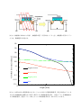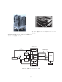
1
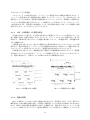
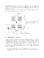
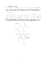
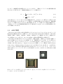
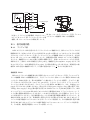
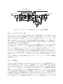
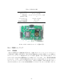
X
CCD
ASIC
2
X
X
X
X
X
CCD
X
CCD
IC
X
CCD
X
CCD
(Application Specific Integrated Circuits : ASIC)
ASIC
CCD
(
0.2 ∼ 15 mV
4
TSMC (Taiwan Semiconductor Manufacturing Company)
0.35 µm CMOS
15 mm
168 mW
IC
CCD
%
CCD
0.2 %
5.5
ASIC
ASTRO-H
2013
ASIC
ASIC
CCD
X
5.4
X
550 km
µV/e−
)
ASTRO-H
30
ASIC
200
(± 10
(FFAST)
·
ASIC
0
ASTRO-H
∼ 40
)
X
ASIC
CCD
ASIC
X
1
1.1
1.2
1.3
1.4
2
2.1
2.2
2.3
2.4
2.5
2.6
2.7
3
3.1
X
X
X
CCD
. .
CCD
.
ASIC
. . . . . . .
. . . . . . . . .
.
.
.
.
.
.
.
.
X CCD (Charge-Coupled Device)
CCD
. . . . . . . . . . . . . . . .
2.1.1 CCD
. . . . . . . . . . .
2.1.2
CCD
X
. . . . . . . . . . . . . . .
2.2.1 X
. . . . . . . . . . .
. . . . . . . . . . . . .
2.3.1 2
3
.
2.3.2
. . . . . . . . . . . .
FDA
. . . . . . . .
. . . . . . . . . . . . .
2.5.1
. . . . . . . . . . . . . .
2.5.2
. . . . . .
2.5.3
. . . . . . . . . . . . . .
CCD
. . . . . . . . . .
2.6.1 CCD
. . . .
. . . . . . . . . . . . .
2.7.1
. . . . . . . . . . .
2.7.2
. . . . . . . . . . . . . . .
2.7.3
. . . . . . . . . . . .
2.7.4
. . . . . . . . . . .
ASIC
X
ASTRO-H
3.1.1
X
SXI . .
3.2 CMOS
. . . . . . . . . .
3.2.1 CMOS
. .
3.2.2 CMOS
.
.
.
.
.
.
.
.
.
.
.
.
1
.
.
.
.
.
.
.
.
.
.
.
.
.
.
.
.
.
.
.
.
.
.
.
.
.
.
.
.
.
.
.
.
.
.
.
.
.
.
.
.
.
.
.
.
.
.
.
.
.
.
.
. . . . . . . . .
. . . . . . . . .
CCD
. . . . . . . . .
. . . . . . . . .
. . . . . . . . .
. . . . . . . . .
. . . . . . . . .
. . . . . . . . .
. . . . . . . . .
. . . . . . . . .
. . . . . . . . .
. . . . . . . . .
. . . . . . . . .
. . . . . . . . .
. . . . . . . . .
. . . . . . . . .
. . . . . . . . .
. . . . . . . . .
. . . . . . . . .
.
.
.
.
.
.
.
.
.
.
.
.
.
.
.
.
.
.
.
.
.
.
.
.
.
.
.
.
.
.
.
.
.
.
.
.
.
.
.
.
.
.
.
.
.
.
.
.
.
.
.
.
.
.
.
.
.
.
.
.
.
.
.
.
.
.
.
.
.
.
.
.
.
.
.
.
.
.
.
.
.
.
.
.
.
.
.
.
.
.
.
.
.
.
.
.
.
.
.
.
.
.
.
.
.
.
.
.
.
.
.
.
.
.
.
.
.
.
.
.
.
.
.
.
.
.
.
.
.
.
.
.
.
.
.
.
.
.
.
.
.
.
.
.
.
.
.
.
.
.
.
.
.
.
.
.
.
.
.
.
.
.
.
.
.
.
.
.
.
.
.
.
.
.
.
.
.
.
.
.
.
.
.
.
.
.
.
.
.
.
.
.
.
.
.
.
.
.
.
.
.
.
.
.
.
.
.
.
.
.
.
.
.
.
.
.
.
.
.
.
.
.
.
.
.
.
.
.
.
.
.
.
.
.
.
.
.
.
.
.
.
.
.
.
.
.
.
.
.
.
.
.
.
.
.
.
.
.
.
.
.
.
.
.
.
.
.
.
.
.
.
.
.
.
.
.
.
.
.
.
.
.
.
.
.
.
.
.
.
.
.
.
.
.
.
.
.
.
.
.
.
.
.
.
.
.
.
.
.
.
8
8
8
8
9
.
.
.
.
.
.
.
.
.
.
.
.
.
.
.
.
.
.
.
.
10
10
10
13
13
14
15
16
16
17
20
20
21
21
22
22
24
24
24
25
26
.
.
.
.
.
27
27
27
28
28
29
3.3
ASIC
. . . . . . . . . . . . . . . . . .
3.3.1 SXI-ASIC
X CCD
3.3.2
. . . . . .
3.4 ASTRO-H
. . .
3.4.1
3.4.2
. . .
4
4.1
SXI-ASIC
ASIC
4.1.1
4.1.2
4.1.3
4.1.4
4.2
4.2.1
4.2.2
4.3
4.3.1
4.3.2
.
.
.
.
.
. .
. . . . .
. . . . .
.
60
/
. . . . .
.
.
.
.
.
.
.
.
.
.
.
.
.
.
.
.
.
.
.
.
.
.
.
.
.
.
.
.
.
.
.
.
.
.
.
.
.
.
.
.
.
.
.
.
.
.
.
.
.
.
.
.
. . . . . . . .
. . . . . . . .
. . . .
.
.
.
.
.
.
.
.
.
.
.
. . . .
.
. . . .
. . . .
. .
. . . .
.
.
.
.
.
.
.
.
.
.
.
.
.
.
.
.
.
.
.
.
.
.
.
.
.
.
.
.
.
.
.
.
.
.
.
.
.
.
.
.
.
.
.
.
.
.
.
.
.
.
.
.
.
.
.
.
.
.
.
.
.
.
.
.
.
.
.
.
.
.
.
.
.
.
.
.
.
.
.
.
.
.
.
.
.
.
.
.
.
.
.
.
.
.
.
.
.
.
.
.
.
.
.
.
.
.
.
.
.
.
.
.
.
.
.
.
.
.
.
.
.
.
.
.
.
.
.
.
.
.
.
.
.
.
.
.
.
.
.
.
.
.
.
.
.
.
.
.
.
.
.
.
.
.
.
.
.
.
.
.
.
.
.
.
.
.
.
.
.
.
.
.
.
.
.
.
.
.
.
.
.
.
.
.
.
.
.
.
.
.
.
.
.
.
.
.
.
.
.
.
.
.
.
.
.
.
.
.
.
.
.
.
.
.
.
.
.
.
.
.
.
.
.
.
.
.
.
.
.
.
.
.
.
.
.
.
.
.
.
.
.
.
.
.
.
.
.
.
.
.
.
.
.
.
.
.
.
.
.
.
.
.
.
.
.
.
.
.
.
.
.
30
31
31
33
33
35
.
.
.
.
.
.
.
.
.
.
.
37
37
37
41
42
42
44
44
55
66
66
68
5
73
A X CCD
74
A.1 Pch-2k4k CCD . . . . . . . . . . . . . . . . . . . . . . . . . . . . . . . . . 74
A.2 X
. . . . . . . . . . . . . . . . . . . . . . . . . . . . . . . . . 74
B SOI CMOS
X
B.1 SOI . . . . . . . . . . . . . . . . .
B.2 ASIC
. . . . . . . . . . . . .
B.3
. . . . . . . . . . .
B.3.1
. . . . . . .
B.3.2
.
B.3.3 AD
. . . . . . . . . .
B.4
. . . . . . . . .
B.4.1
. . . . . . . . . .
B.4.2 M iKE
. . . . .
B.4.3
. . . . . . . .
B.4.4
. . .
B.5 ASIC
. . . . . . . . . .
B.6 X CCD
. . . . .
CCD
.
.
.
.
.
.
.
.
.
.
.
.
.
2
.
.
.
.
.
.
.
.
.
.
.
.
.
.
.
.
.
.
.
.
.
.
.
.
.
.
.
.
.
.
.
.
.
.
.
.
.
.
.
.
.
.
.
.
.
.
.
.
.
.
.
.
ASIC
.
.
.
.
.
.
.
.
.
.
.
.
.
.
.
.
.
.
.
.
.
.
.
.
.
.
.
.
.
.
.
.
.
.
.
.
.
.
.
.
.
.
.
.
.
.
.
.
.
.
.
.
.
.
.
.
.
.
.
.
.
.
.
.
.
.
.
.
.
.
.
.
.
.
.
.
.
.
.
.
.
.
.
.
.
.
.
.
.
.
.
.
.
.
.
.
.
.
.
.
.
.
.
.
.
.
.
.
.
.
.
.
.
.
.
.
.
.
.
.
.
.
.
.
.
.
.
.
.
.
.
.
.
.
.
.
.
.
.
.
.
.
.
.
.
.
.
.
.
.
.
.
.
.
.
.
.
.
.
.
.
.
.
.
.
.
.
.
.
.
.
.
.
.
.
.
.
.
.
.
.
.
.
.
.
.
.
.
.
.
.
.
.
.
.
.
.
.
.
.
.
.
.
.
.
.
.
.
.
.
.
.
.
.
.
.
.
.
.
.
.
.
.
.
.
.
.
.
.
.
.
.
.
.
76
76
76
78
78
79
79
81
81
82
82
82
84
86
B.6.1 X
B.6.2 X
B.6.3
. . . . . . . . . . . . . . . . . . . . . . . . . . . . . 86
. . . . . . . . . . . . . . . . . . . . . . . . . . . . . . 86
. . . . . . . . . . . . . . . . . . . . . . . . . . . . . . . . . . 88
3
2.1
2.2
2.3
2.4
2.5
2.6
2.7
2.8
2.9
2.10
2.11
2.12
2.13
CCD
MOS
3.1
3.2
3.3
3.4
3.5
3.6
3.7
3.8
3.9
3.10
ASTRO-H
NMOS
SXI-ASIC
SXI-ASIC
∆Σ ADC
4.1
4.2
4.3
4.4
4.5
4.6
4.7
4.8
4.9
.
.
.
.
.
.
.
.
.
.
.
.
.
.
.
.
.
.
.
.
.
.
.
.
.
.
.
.
.
.
.
.
.
.
.
.
.
.
.
.
.
.
.
.
.
.
.
.
.
.
.
.
.
.
.
.
.
.
.
.
.
.
.
.
.
.
.
.
.
.
.
.
.
.
.
.
.
.
10
11
13
16
16
17
18
19
19
20
21
21
23
.
.
.
.
.
.
TID
.
ASTRO-H
.
SEE
. . . . . . . . . . . . . . . . . . . . . . .
Weibull curve . . . . . . . . . . . . . . . . . . . . . . . . . . . . .
.
.
.
.
.
.
.
.
.
.
.
.
.
.
.
.
.
.
.
.
.
.
.
.
.
.
.
.
.
.
.
.
.
.
.
.
.
.
.
.
.
.
.
.
.
.
.
.
.
.
28
29
30
31
32
32
34
34
36
36
.
.
.
.
.
.
.
.
.
.
.
.
.
.
.
.
.
.
.
.
.
.
.
.
.
.
.
.
.
.
.
.
.
.
.
.
.
.
.
.
.
.
.
.
.
38
38
39
40
41
42
43
43
44
3
2
FDA
CCD
CCD
CCD
. . . . . . . . . . . . . . .
. . . .
CCD
CCD
CCD
. . . . . . . . . . . . .
CCD
. . . . . . . . . . . . .
CCD
.
. . . . . . . . . . . . .
. . . . . . . . . .
(
26 )
. . . . . . . . . . . . . . . . . . . .
. . . . . . . . . . . .
. . . . . . . . . . . . . . . . .
. . . . . . . . . . . . . . .
( http://astro-h.isas.jaxa.jp)
NMOS PMOS
. . . .
. . . . . . . . . . . . . . . . . . . . . . .
. . . . . . . .
AD
. . . . . . . . . .
. . . . . . . . . . . . . . . . . .
. . . . . . . . . . . . . . . . . . .
.
.
.
.
.
.
.
.
.
.
.
.
.
.
.
.
.
.
.
.
.
NI
.
.
.
.
.
.
.
.
.
.
.
.
.
.
.
.
.
.
.
.
.
.
.
.
.
.
.
.
.
. . . . . .
channel 0 even INL .
60
. . . . . . . . . . .
. . . . . . . . . . .
. .
. . . . . . . . . . .
. . . . . . . . . . .
. . . . . . . . . . .
. . . . . . . . . . .
. . . . . . . . . . .
−60
. . .
. . . . . . . . . . .
. . . . . . . . . . .
. . . . . . . . . . .
. . . . . . . . . . .
.
.
.
.
.
.
.
.
. . .
. . .
. . .
. . .
. . .
. . .
INL
.
.
.
.
.
.
.
.
.
.
.
.
.
. . .
. . . . . . . . .
4
.
.
.
.
.
.
.
.
.
.
.
.
.
.
.
.
.
.
.
.
.
.
.
.
.
.
.
.
.
.
.
.
.
.
.
.
.
.
.
.
.
.
.
.
.
.
.
.
.
.
.
.
.
.
.
.
.
.
.
.
.
.
.
.
.
.
.
.
.
.
.
.
.
.
.
.
.
.
.
.
.
.
.
.
.
.
.
.
.
.
.
.
.
.
.
.
.
.
.
.
.
.
.
.
.
4.10
4.11
4.12
4.13
4.14
4.15
4.16
4.17
4.18
4.19
4.20
60
60
1
1
2
2
DAC
4.21
4.22
4.23
4.24
4.25
4.26
4.27
4.28
4.29
4.30
4.31
4.32
4.33
4.34
4.35
4.36
4.37
4.38
4.39
4.40
4.41
4.42
4.43
4.44
4.45
. . . . . . . . . . . . . . . . . . . .
. . . . . . . . . . . . . . . . . . . . .
. . . . . . . . . . . . . . . . .
. . . .
. . . . . . . . . . . . . .
. . . . . . . . . . . .
. . . . . . . . . . . . .
. . . . . . . . . . . .
. . . . . . . . . . . . .
(20 krad
5-bit DAC
0) . . . . . . . . . . . . . . . . . .
(20 krad
(20 krad
HIMAC
HIMAC
. . . . . . . .
. . . .
. . . .
2
.
. . . . . .
. . . . . .
. . . . . .
.
. . . . . .
ASIC
ASIC
ASIC
channel 0 even
LET
. . . . . . . . . . . . . .
ASTRO-H
NI
. . . . . . . . . . . .
. . . . . . . . . . . . . . .
0∼40
. . . . . . .
.
.
.
.
.
.
.
.
.
. . . . . . . . . . . .
. . . . . . . . . . . .
. . . . . . . . . . . .
. . . . . . . . . . . .
. . . . . . . . . . . .
. . . . . . . . . . . .
. . . . . . . . . . . .
. . . . . . . . . . . .
. . . . . . . . . . . .
0) . . . . . . . . . .
(20 krad
5-bit
. . . . . . . . . . . . . . . . . .
5-bit DAC 0) . . . . . .
5-bit DAC 0) . . . . . .
20 krad
5-bit DAC 3
200 krad
5-bit DAC 0
200 krad
5-bit DAC 3
. . . . . . . . . . . . . . . . . .
. . . . . . . . . . . . . . . . . .
. . . . . . . . . . . . . . . . . .
. . . . . . . . . . . . . . . . . .
. . . . . . . . . . . . . . . . . .
. . . . . . . . . . . . . . . . . .
. . . . . . . . . . . . . .
(chip7) . . . . . . . . . . . .
(chip12) . . . . . . . . . . .
(chip13) . . . . . . . . . . .
. . . . . . . . . .
. . . . . . . . . . . . . . . . . .
. . . . . . . . . . . . . . . . . .
. . . . . . . . . .
. . . . . . . . . . . . . . . . .
. . . . . . . . . . . . .
. . . . . . . . . . . . . . . . . .
. . . . . . . . . . . . . . . . . .
. . . . . . . . . . . . . . . . .
. . . . . . . . . . . . . . . . . .
45
45
46
47
47
48
48
49
49
51
51
52
52
53
54
55
56
57
57
57
58
60
60
62
62
62
63
65
66
67
67
69
70
70
71
72
A.1 Pch-2k4k CCD
. . . . . . . . . . . . . . . . . . . . . . . . . . . . . 74
A.2 X
. . . . . . . . . . . . . . . . . . . . . . . . . . . . . . . . . 75
5
B.1
B.2
B.3
B.4
B.5
B.6
B.7
B.8
B.9
B.10
B.11
B.12
B.13
B.14
B.15
B.16
CMOS SOI CMOS . . . . . . . . . . . . . . . . . . . . .
ASIC
. . . . . . . . . . . . . . . . . . . . . . . . . . . . . .
. . . . . . . . . . . . . . . . . . . . . . . . . . . . . .
. . .
. . .
2
ADC
. . . . . . . . . . . .
1 . . . . . . . . . . . . . . . . . . . . . . . . . . . . . . .
2 . . . . . . . . . . . . . . . . . . . . . . . . . . . . . . .
CCD ASIC
. . . . . . . . . . . . . .
M iKE
. . . . . . . . . . . . . . . . . . . . . . . . . . .
. . . . . . . . . . . . . . . . . . . . . . . . .
. . . . . . . . . . . . . . . . . . . . . .
. . .
. . . . . . . . . . . . . . . . . . . . . . . . . . . . . . . .
X
. . . . . . . . . . . . . . . . . . . . . . . . . . . .
X
. . . . . . . . . . . . . . . . . . . . . . . . . . . . .
6
.
.
.
.
.
.
.
.
.
.
.
.
.
.
.
.
.
.
.
.
.
.
.
.
.
.
.
.
.
.
.
.
.
.
.
.
.
.
.
.
.
.
.
.
.
.
.
.
.
.
.
.
.
.
.
.
.
.
.
.
.
.
.
.
.
.
.
.
.
.
.
.
.
.
.
.
.
.
.
.
77
77
78
78
79
80
80
80
81
83
83
83
85
85
87
87
3.1
4.1
4.2
4.3
4.4
4.5
4.6
4.7
4.8
4.9
4.10
4.11
4.12
SXI-ASIC
. . . . . . . . . . . . . . . . . . . . . . . . . . . . . . . . . 31
2
. . . . . . . . .
60
4.19∼
HIMAC
4.25
4.31
4.32
ADC
. . . . . .
‘MND02’
. . . . . . . . .
. . . . . .
2
LET = 1.68 MeV·cm /mg
4.42
A.1 Pch-2k4k CCD
A.2 Pch-2k4k CCD
. . . . . . . . . . . . . . . . . 37
. . . . . . . . . . . . . . . . . . . . . . . . 44
. . . . . . . . . . . . . . . 50
50
. . . . . . . . . . . . . . . . . . . . . . . . 55
. . . . . . . . . . . . 56
ADC
. . . . . . . . . . . . . . . . . . . . . . . . 60
. . . . . . . . . . . . . . . . . . . . . . . . 61
Integral flux (particle/cm2 /str/sec) . . 64
. . . . . . . . . . . . . . . . . 66
. . . . . . . . . . . . . . . . . . 68
. . . . . . . . . . . 70
. . . . . . . . . . . . . . . . . . . . . . . . . . . . . 75
. . . . . . . . . . . . . . . . . . . . . . . . . 75
B.1 ASIC
. . . . . . . . . . . . . . . . . . . . . . . . . . . . . . . . . . . . 77
B.2 X CCD
. . . . . . . . . . . . . . . . . . . . . . . . . . . . . . . . . 81
B.3 X CCD
. . . . . . . . . . . . . . . . . . . . . . . . . . . . . . . 86
7
1
1.1
X
X
CCD
X
CCD
1993
X CCD
(SIS Solid-State Imaging Spectrometer)
X
X
(
)
X CCD
X CCD
X
4 keV
X
X
Chandra
XMM-Newton
X
X
X
CCD
1.2
X
X
X
CCD
X
X
[3][4]
CCD
CCD
CCD
X
CCD
X
CCD
CCD X
2
)
(
CCD
1
1
1
10
1.3
CCD
ASIC
CCD
X
CCD
IC
X
(Application Specific Integrated Circuits : ASIC)
X CCD
ASIC
Newton
PN-CCD
8
CCD
XMM[7]
ASIC
AD (Analog-to-Digital)
AD
AD
ASIC
ASIC
(LSI)
OPEN IP[16]
Noqsi Aerospace
ASIC
X
CCD
John
P. Doty
1.4
ASIC
X
ASTRO-H
2
1
·
1
ASIC
2
ASIC
4
X
ASIC
ASIC
CCD
5
A
CCD
ASIC
B
9
ASIC
X
ASIC
ASIC
3
ASIC
CCD
X
2
2.1
X
CCD (Charge-Coupled Device)
CCD
CCD(
)
1970
AT&T
Boyle
1
CCD
Smith
CCD
MOS(Metal Oxide Semiconductor)
( 2.1)
CCD
[12]
electrode
Metal
electrode
electrode
Metal
Metal
Oxide
Semiconductor
Potential
Transfer direction
charge
2.1: CCD
1
2
(poly-Si)
2.1.1
MOS
2
CCD
(SiO2 )
CCD
SiO2
µm
CCD
CCD
3
2.2
a.
10
[27]
2.2: MOS
EI
Ec
EV
(a)
EF
([27]
(b)
)
11
(c)
pp
pp = ni exp(
EI − EF
)
kT
(2.1)
ni
(
EF
EI
2.2 (a))
b.
P
(
)
(
(
NA
)
2.2 (b))
Qs
ρs
ρs = −eNA
(2.2)
Qs = −eNA xd
(2.3)
xd
eNA
d2 φ
=
2
dx
ε
)
xd (
dφ
=0
dx
φ = φs
(2.4)
φs
φ=
(2.4)
0
(x = xd )
(2.5)
(x = 0)
(2.6)
(2.5) (2.6)
eNA 2 eNA xd
x −
x + φs
2ε
ε
φ(x = xd ) = 0
(2.7)
xd
xd =
!
2εφs
eNA
(2.8)
c.
EF
np
EI
EF − EI
np = ni exp(
12
EF − EI
)
kT
(2.9)
(
10∼100 Å
(
CCD
CCD
CCD
CCD (Buried channel CCD)
CCD
2.3
CCD
CCD
CCD
p
Si
CCD (Surface
CCD
2
+V
Si
SiO2
Si-SiO2
CCD
2.3:
2.2
CCD
p
Si
n
CCD
Si
CCD
X
Si
1
Si
X
)
n
2.1.2
MOS
channel CCD)
(
)
2.2 (c))
CCD
Si
2
CCD
X
X
13
2.2.1
X
X
3
1.
(photoabsorption)
2.
(Compton scattering)
3.
(pair creation)
CCD
100 eV 10 keV
X
X
10 keV
10 keV
CCD
CCD
X
X
CCD
Ephoton
(Photoelectron)
Eelectron
Eelectron = Ephoton − Ebinding
(2.10)
1
Ebinding
Si
X
Eelectron
W
Nelectron =
Nelectron
W
Nauger =
(2.11)
Si
2
Ebinding
W
(2.12)
N
Nauger
N=
Ephoton
Eelecton Ebinding
+
=
W
W
W
(2.13)
X
5.9 keV
1600
X
1
2
X
X
1.8 keV
K
10 keV
14
W =3.65[eV]
X
X
(1.74 keV)
CCD
X
1.83 keV
X
Si
20µm
Si
X
CCD
Si
X
X
1.74 keV
2.3
CCD
2
−
CCD
CCD
X
CCD
CCD
CCD
CCD
CCD
CCD
1
X
X
CCD
CCD
MOS
CCD
X
CCD
15
CCD
CCD
CCD
CCD
CCD
CCD
CCD
2.3.1
2
3
1
3
3
CCD (
2.4)
2
CCD (
2.5)
CCD 2
CCD
2
CCD
2.4: 3
CCD
2
2.5: 2
CCD
2.3.2
2.6
CCD
2
Gate)
TG
16
P1V P2V
TG (Transfer
P2V
P1H P2H
2
SG (Summing Gate)
SG
TG
P2H
1
ISV IG1V IG2V ISH IG1H IG2H
ISV ISH RD
2.6:
2.4
-
CCD
FDA
CCD
CCD
( 2.7)
FET (MOS FET2)
(RD:Reset Drain)
(OG:Output Gate)
(OS:Output Source)
1. SG
RG
Floating diffusion
FDA
FET
FET
MOS-FET
FDA (Floating Diffusion Amplifier)
FET (MOS FET1)
(RG:Reset Gate)
(OD:Output Drain)
FET
MOS FET1
( 2.7 (1) )
RD
Floating diffusion
RD
17
2.7: FDA
18
2. RG
MOS FET1
MOS FET2
OD
floating level
(
2.7 (2) )
SG
SG
3. SG
diffusion
MOS FET2
floating diffusion
1∼3
(
2.7 (3) )
SG
floating
signal level
3
CCD
2.8
CCD
floating level signal level
2.9
26
2.8: CCD
1 pixel
Reset pulse
Floating level
0V
Signal level
2.9: CCD
3
V
RD
OG
Q
(
26
C
19
)
V=Q/C
−60
CCD
2.5
CCD
2.8
floating
floatinglevel
signal level
signal level
2.5.1
A/D
floating signal level
CCD
f
X
X
CCD(SIS)
5
2.10:
20
[6]
2.5.2
floating
signal level
ADC
CCD
N† Sampling
SC
[6]
N† Sampling
2.11:
2.5.3
floating,signal level
[6]
2.12:
21
2.6
CCD
CCD
X
X
CCD
X
X
X
CCD
CCD
(
[6])
2.6.1
CCD
CCD
2.13
CCD
10
CCD
CCD
512×512
CCD
2.13
CCD
24µm×24µm
600×600
VOC(Vertical Over Clock)
HOC(Horizontal Over Clock)
2.7
• HOC
HOC
CCD
HOC
• VOC
VOC
VOC
HOC
•
CCD
(
)
X
X
X
VOC
2.13
1
X
X
CCD
CCD
(
2 3
[6])
22
1
55 Fe
1
2 3
2.13: X
10
HOC
X
2 ×2
23
VOC
2.7
CCD
(
)
2.7.1
CCD(
)
E [eV]
N=
X
E
W
N
(2.14)
W
∆N =
∆N =
N=
!
E
W
NF =
!
F
√
√
(2.15)
E
W
(2.16)
F =0.12
F
∆E(F W HM ) = 2.35 × W ×
CCD
6keV
X
∆E(F W HM ) = 2.35 × 3.65 [eV ] ×
#
"
(∆N )2 [eV ]
0.12 ×
6000 [eV ]
∼ 120 [eV ]
3.65 [eV ]
(2.17)
(2.18)
CCD
∆E(F W HM ) =
F W HM noise
$
2
1202 + F W HMnoise
[eV ]
2.7.2
CCD
1
(e− /pixel/
)
1.
24
(2.19)
2. Si-SiO2
3.
2
2.1.1
MPP
3
[8]
(
T
Eg
)
2kB T
Eg
VOC
)
(
(
) ∝ T 1.5 exp(−
kB
X
(
) ≡
(
×
(2.20)
(
)
) − (VOC
)
)
(2.21)
W
VOC
VOC
eV
Si
1
(
$
) ≡
×
(
(
)2 − (VOC
)
)2
(2.22)
W
2.7.3
VOC
HOC
(
VOC
) ≡ ((VOC
(
×
W
) − (HOC
)
HOC
))
(2.23)
spurious charge
spurious charge
CCD
Janesick
[9]
CCD
25
CCD
spurious
charge
spurious charge
Janesick
(1997 )
spurious charge
[10]
(2000
)
[11]
2.7.4
FDA
FET
HOC
[12]
(
) ≡ (HOC
)×
HOC
26
(
)
W
(2.24)
3
ASIC
ASIC
ASIC
CMOS
ASTRO-H
ASIC
3.1
X
X
ASTRO-H
X
ASIC
ASTRO-H
ASTRO-H
X
3.1
X
ASTRO-H
X
2013
)
3
(
2
X
X
X
(
X
X
)
0.3 600 keV
3.1.1
X
X
SXI
(Soft X-ray Imager : SXI)
0.3 20 keV
X
X
CCD
SXI
SXI
X
CCD
X
CCD X
CCD X
X
CCD
SXI
20 keV
X
ASTRO-H
CCD
27
4
P
10 %
3.1: ASTRO-H
3.2
CMOS
3.2.1
CMOS
(
http://astro-h.isas.jaxa.jp)
CMOS
LSI
LSI
CMOS
[14]
LSI
28
CMOS
CMOS
3.2.2
CMOS
G
b)
a)
GATE
B
S
D
D
S
W
L
SOURCE
DRAIN
N+
P+
B
G
G
B
N+
S
D
NMOS
PMOS
gate insulator
p-type substrate
3.2:
NMOS
p
Transistor)
p
a)
NMOS b)
PMOS
n
MOSFET(Metal Oxide Semiconductor Field Effect
3.2
NMOS
a) b)
NMOS
MOSFET PMOS
NMOS
MOSFET
NMOS p
n
(DRAIN)
(SOURCE)
(SiO2 )
(D)
(G)
(S)
(B) 4
ID
(Vth )
ID
NMOS
PMOS
n
p
3.2
p
n
/
NMOS
NMOS
PMOS NMOS
CMOS (Complementary-MOS)
2
MOSFET
MOSFET
VGS
Vth
ID
(VDS < VGS −Vth )
(VDS > VGS −Vth )
ID
%
&
1
W
µ Cox (VGS − Vth ) − VDS VDS
ID =
L
2
W
µ
29
L
(3.1)
(
3.2
)
Cox
ID
ID =
≈
W
µ Cox (VGS − Vth )2 (1 + λVDS )
2L
βW
(VGS − Vth )2
2L
(3.2)
(3.3)
VDS
λ
ID
ID
(VGS -Vth)
2
[14][15]
3.3
VGS
3.3
ASIC
SXI CCD
X
CCD
ASIC 4
ASIC SXI-ASIC
SXI-ASIC
‘MD01’ ‘MND01’ ‘MD02’ ‘MND02’
‘MND02’
4.2.2
‘MD01’
SXI-ASIC X CCD
4
3.3 V
5-bit DAC (Digital to Analog Converter)
2
∆Σ ADC (Analog to Digital Converter)
TSMC (Taiwan
Semiconductor Manufacuturing Company) 0.35 µm CMOS
3 mm
15 mm
QFP(Quad Flat Package)
QFP
3.3
3.1 SXI-ASIC
3.3:
QFP
QFP
30
3.1: SXI-ASIC
TSMC 0.35 µm CMOS
3 mm × 3 mm
15 mm × 15 mm
4
3.3 V
3.4: SXI-ASIC
3.3.1
3.4
SXI-ASIC
X
CCD
SXI-ASIC
ASIC
10
X
CCD
0.63
5-bit DAC
5-bit DAC
32
∆Σ ADC
3.5
∆Σ ADC
Deint Int P ost
3.5
SXI-ASIC
CCD
Int
155
2
CCD
∆Σ ADC even ADC
Reset
ADC
1
Reset
odd ADC
Deint
CCD
2
Int
P ost
ADC
155-bit
AD
SXI-ASIC
AD
DAQ
12-bit
3.3.2
SXI-ASIC
3.6
∆Σ ADC
31
155-bit
12-bit
1 pixel readout time
CCD
signal
Deint
odd ADC
35clocks
Int
Post
35clocks
85clocks
Reset
even ADC
5clocks
Deint
35clocks
Int
Post
35clocks
85clocks
Reset
5clocks
3.5: ∆Σ ADC
AD
0.04
Filter coefficient
0.03
0.02
0.01
0
0
20
40
60
80
100
Sample number (clock)
3.6:
32
120
140
160
bit
Y(n) n = 1 ∼ 155
155
'
n=1
Y (n) × W (n)
(
W (n) =
12-bit
+1 if Y (n) = 1
−1 if Y (n) = − 1
(3.4)
W (n)
W (n)
AD
mathematica
W(n)
3.4
[19]
ASTRO-H
ASTRO-H
LEO)
SXI-ASIC
550km
[24]
30
(Low Earth Orbit :
ASTRO-H
3.4.1
Total Ionizing Dose(TID)
Total Ionizing Dose (TID)
TID
LSI
NMOS
TID
3.7
TID
1 joule/kg ≡ 1 Gy = 100 rad
3.8
SHIELDOSE-2
(3.5)
[25]
3
1 mm
1.1 krad
SXI-ASIC
10
22 krad
TID
60
33
1
2
3.7:
NMOS
·
106
105
Absorbed dose rate [rad/year]
104
1000
100
10
Trapped electron
1
0.1
Trapped proton
0.01
10−3
Bremsstrahlung
Total
0.1
1
Depth [mm]
3.8: ASTRO-H
3
34
10
Sigle Event Effect(SEE)
Sigle Event Effect(SEE)
SEE
SEU(Single Event Upset)
TID
SEL(Single Event Latchup)
2
SEU
SEU
3.9
5V
0V
PMOS
·
·
0V
3.9
5V
GND
5V
CMOS
[17] LSI
LSI
ON
SEL
LSI
(Linear
Energy Transfer : LET)
LET
MeV·cm2 /mg
SEE
SEE
LET
[18] Weibull curve
LSI
LET
LET
LET
SEE
LET
3.10
SEE
Weibull curve
%
%
&&
L − Lth
σSEE (L) = S0 · 1 − exp −
W
σSEE = S0
width
JAXA
MeV·cm2 /mg
L
SEE
SEL
(3.6)
LET Lth
LET
(L > Lth ) W
SEU
LET
75MeV·cm2 /mg
curve
LET
25
LET
LET
SEE
SEE
LET
3.4.2
ASTRO-H
ASIC
±10
10
·
CMOS
0
SXI-ASIC
∼40
35
30
3.9:
PMOS
3.10: Weibull curve
36
4
SXI-ASIC
4.1 ASIC
4.3 ASIC
4.1
4.2
ASIC
SXI-ASIC
ASIC
CCD
ASIC
4.1.1
4.1
CCD
ASIC
NI6534
NI6534
MHz
ASIC
NI6703
NI6534
NI
4.2
first-in first-out memory(FIFO)(1) FIFO(2)
National Instrumemts
NI6703 NI6534 PCI
CCD
CCD
ASIC
ASIC
100 MHz
ASIC
FIFO(2)
NI6703
NI6703
FIFO(1)
1.5625
CCD
819
+16 mV
2 mV
5-bit DAC
0
1
-18 mV
10
18
5-bit DAC
CCD
5-bit DAC
0
0V
DAC
4.1
4.1:
[kHz]
5-bit DAC
[mV]
19.5, 39.1, 78.1, 156, 312, 625
0
10
-18 ∼ +16
37
5-bit DAC
4.1: [ ]
[ ] NI
5-bit DAC setup
NI6703
switching pattern
PCI/IO channel
Test board
analog signals
CCD
simulator
ASIC
FIFO(1)
FIFO(2)
control signals
NI6534
bitstreams
clock frequency setup
4.2:
38
clock
divider
670
channel0 even
530
channel0 odd
660
Decimal value
Decimal value
520
510
650
640
500
630
490
0
100
200
300
400
500
600
700
800
900
0
100
200
300
Pixel number
400
500
600
700
800
900
Pixel number
340
channel1 even
channel1 odd
350
Decimal value
Decimal value
330
320
310
340
330
320
300
310
0
100
200
300
400
500
Pixel number
600
700
800
900
0
channel2 even
100
200
300
400
500
Pixel number
600
700
800
900
300
400
500
Pixel number
600
700
800
900
300
400
500
Pixel number
600
700
800
900
channel2 odd
510
280
Decimal value
Decimal value
500
270
260
490
480
250
470
240
0
100
200
300
400 500
Pixel number
600
700
800
900
0
channel3 even
100
200
channel3 odd
500
Decimal value
Decimal value
340
330
320
490
480
470
310
460
300
0
4.3: 819
100
200
300
400
500
Pixel number
600
700
800
900
0
CCD
100
200
ASIC
39
channel0 even
channel0 odd
200
150
150
counts
Counts
200
100
100
50
50
0
460
0
480
500
520
Pulse height (ch)
540
560
600
620
640
660
680
Pulse height (ch)
channel1 even
channel1 odd
150
150
Counts
200
Counts
200
100
100
50
50
0
0
280
300
320
Pulse height (ch)
340
360
300
channel2 even
320
340
Pulse height (ch)
360
380
channel2 odd
200
150
150
Counts
Counts
200
100
100
50
50
0
0
220
240
260
280
Pulse height (ch)
300
460
channel3 even
480
500
Pulse height (ch)
520
540
channel3 odd
150
150
Counts
200
Counts
200
100
100
50
50
0
0
280
300
320
340
Pulse height (ch)
360
440
4.4:
40
460
480
500
Pulse height (ch)
520
Residual (%)
Decimal value
4500
4000
3500
3000
2500
2000
1500
1000
500
0
0.15
0.1
0.05
0
-0.05
-0.1
-0.15
(a)
data
model
(b)
-20
-15
-10
-5
0
5
10
15
20
Voltage difference (mV)
4.5: (a)
78.1 kHz
0
CCD
0.2 %
INL
even ADC
12 bit
ADC
(b)
4.1.2
(Integral Non linearity : INL)
ADC
2 mV CCD
(EVEN ADC ODD ADC)
8
ADC
-18 mV
0
+16 mV
ADC
78.1 kHz
ASIC 2
∆Σ ADC
4.3
4
4.4
18
ADC
even ADC
4.5
ADC
78.1 kHz
/XIS
4.1
0.2 %
INL
[33]
156 kHz
INL (%) =
INL
2
ADC
-18 mV
+16 mV
4.6
∆Σ ADC
2
ADC
INL
INL
× 100
41
0.1∼0.3 %
(4.1)
INL [%]
1
0.5
0
10
4.6:
∆Σ ADC
∆Σ ADC
INL
100
Readout speed [kHz]
1000
INL
156 kHz
0.1∼0.3 %
4.1.3
4.4
4.5
[ch/mV]
4.7
ADC
78.1
8
28.5 ∼ 31.4 µV
29.8 ± 0.1 µV
CCD
kHz1
∆Σ ADC
∆Σ ADC
CCD
[µV]
[µV/e− ]
[e− ] =
SXI
Pch-2k4k CCD
(4.2)
5.5 µ V/e−
5.4
4.1.4
4.8
ASIC 1
156 kHz
168 mW
ASIC
Ω
LVDS
ASIC
168 mW
ASIC
1
SXI
68kHz
42
ASIC
ASIC
IC
3.3 V
8
3.5 mA
100
3.5 mA × 3.3 V × 8 = 92.4 mW
Equvalent input noise [µV]
100
50
0
10
100
Readout speed [kHz]
4.7:
∆ΣADC
28.5 ± 0.3 ∼ 31.4 ± 0.3 µV
1000
∆Σ ADC
200
Power consumption [mW]
180
160
140
120
10
100
Readout speed [kHz]
4.8:
ASIC1
43
1000
60
27 Co
β−
2.505
γ1
1.332
γ2
0
60
28 N i
4.9:
60
γ 1 :1.173 MeV γ 2 :1.332 MeV
4.2
4.2.1
60
2009
6
1
60
4
2
SXI-ASIC
TID
60
2
4.2
2
4.2:
[TBq]
[rad/hr]
60
2
279
4 m × 4 m × 3.1 m
0.1 ∼ 50
5.3
4.9
60
60
4.9
60
60
1.173 MeV
2
1.332 MeV
ASIC
4.10
60
680 mm
4.11
30 cm
10 mm
44
4.12
2
4.10:
5
6
mm
30mm
50mm
2300∼3000mm
4.11:
45
4.12:
4.13
2009
6
1
200 krad
0.35 µm CMOS
1
7
2
0.9
2008
(Heavy Ion Medical Accelerator in Chiba : HIMAC)
SXI-ASIC 1
MD01
[28][20]
16 krad
20 krad
2
SXI-ASIC
LSI
krad
200 MeV/amu
4.13
cm 2
60
6
200 krad
4.15
20 krad
ASIC
45.3 cm
144 cm
ASIC
ASIC
ASIC
15 cm
MeV
4.5 ×
10−5
4.16
2
ASIC
2.5 cm
12.5 cm
IC
1.25
ASIC
45.3 cm
2.5 cm
× 10−4
144
1
12.5 cm
4.18
0.19 2.4
1.25 MeV
(∼25 )
4.14
6
46
水に対する吸収線量率 (Gy/hour)
1Gy=100rad
2日目
7時間照射で200krad
28.6 krad/hour
1日目
6時間照射で20krad
(Si換算)
3.33 krad/hour
(Si換算)
45.3cm
144cm
線源から試料までの距離 (cm)
4.13:
60
Si
0.9
4.14:
6
47
4.15:
(1
4.16: [ ]
37 cm
28.1 cm
48
)
[ ] ASIC
4.15
4.17:
(2
4.18: [ ]
ASIC
2.5 cm
[ ] ASIC
4.17
)
12.5 cm
30 cm
24 cm
49
6
78.1 kHz
3
1
-14 mV ∼ +14 mV
4.3:
10
5-bit DAC
4.3
60
[kHz]
5-bit DAC
[mV]
• 1
0
5-bit DAC
0 3 2
-10 mV ∼ +18 mV 5-bit DAC
5
78.1
10
0,3
-10 ∼ +18 (5-bit DAC
-14 ∼ +14 (5-bit DAC
0)
3)
: 20krad
1
3.33 krad/hr
INL
4
[ch/mV]
4.20
INL
3
6
20 krad
[ch/mV]
4.19
4.21
5-bit DAC
4.22
4.23 5-bit DAC
[ch/mV]
0
INL
5-bit DAC
4.4:
0 3
4.19∼
! channel 0 even
∗ channel 0 odd
4.25
ADC
+ channel 1 even
! channel 1 odd
× channel 2 even
* channel 2 odd
50
( channel 3 even
♦ channel 3 odd
124
gain (ch/mV)
122
120
118
116
0
4.19: 5-bit DAC
5
10
absorbed dose (krd)
15
5
10
absorbed dose (krd)
15
20
0
gauss sigma of scatter plot (ch)
6
4
2
0
0
4.20: 5-bit DAC
0
51
20
equivalent input noise (µV)
40
38
36
34
32
30
0
4.21: 5-bit DAC
5
10
absorbed dose (krd)
15
20
5
10
absorbed dose (krd)
15
20
0
0.4
INL (%)
0.3
0.2
0.1
0
0
4.22: 5-bit DAC
0
52
6
gauss sigma of scatter plot (ch)
124
gain (ch/mV)
122
120
118
4
2
116
0
5
10
absorbed dose (krd)
15
0
20
5
10
absorbed dose (krd)
15
20
0
5
10
absorbed dose (krd)
15
20
0.4
40
38
0.3
36
INL (%)
equivalent input noise (µV)
0
34
0.2
0.1
32
30
0
5
4.23: 5-bit DAC
10
absorbed dose (krd)
15
0
20
3
53
6
gauss sigma of scatter plot (ch)
125
gain (ch/mV)
120
115
110
0
50
100
absorbed dose (krd)
150
2
0
200
45
0
50
100
absorbed dose (krd)
150
200
0
50
100
absorbed dose (krd)
150
200
0.4
0.3
40
INL (%)
equivalent input noise (µV)
4
0.2
0.1
35
0
50
100
absorbed dose (krd)
4.24: 5-bit DAC
• 2
150
0
200
0
: 200 krad
20 krad
200 krad
[ch/mV]
1
0
4.24
INL
(20 krad)
4.24
5-bit DAC
3
5-bit DAC
0
ADC
! channel 0 even
∗ channel 0 odd
! channel 0 even
200 krad
channel 0 odd
200krad
4.25
4.25
5-bit DAC
5∼6%(
180 krad
36 µV →
(ch/mV) 30 krad
even odd ADC
30 krad
∗ channel 0 odd
38 µV )
INL
0.4%
3
5-bit DAC
0
54
6
gauss sigma of scatter plot(ch)
125
gain (ch/mV)
120
115
110
0
50
100
absorbed dose (krd)
150
4
2
0
200
0
50
100
absorbed dose(krd)
150
50
100
absorbed dose (krd)
150
200
45
0.6
INL (%)
equivalent input noise (µV)
0.8
40
0.4
0.2
35
0
50
100
absorbed dose(krd)
4.25: 5-bit DAC
4.2.2
150
0
200
3
/
2009
7
7
8
HIMAC
4.26
HIMAC
60
ASIC
150 MeV
2.7 mm
4.5
4.9 mm
2
HIMAC
LET
400 MeV
3 mm
3.3
4.5
1
LET
[21]
4.5: HIMAC
[MeV/amu]
(
) [mm]
[particle/sec]
LET [MeV·cm2 /mg]
55
150
2.7
0.56
≤ 2 × 10 8
4.38 × 10 −3
400
4.9
0.19
≤ 2 × 10
1.68
6
200
4.26:
(Heavy Ion Medical Accelerator in Chiba : HIMAC)
4.27
4.28
ASIC
ASIC
3.1 mm
150 MeV
( 5%)[21]
3.1 mm
4.29
2
2
SEL
0.2 A
SEL
3.3 V
5
·
0.1 Ω
4.6
4.6:
[kHz]
5-bit DAC
[mV]
[A]
56
78.1
10
3
-24 ∼ +14
0.2
4.27: HIMAC
4.28:
4.29:
2
57
Absorbed dose [krad]
150
100
50
0
0
20
40
Transit time [min]
60
80
4.30:
60
SXI-ASIC
TID
2008
HIMAC
1.11 ×
SXI-ASIC
: 200 MeV/amu
108
particle/sec
‘MD01’
2.00 × 10⁶ particle/sec
63
LET
15
ASIC
ELET
ST [cm2 ]
ELET
[ Gy = J/kg = 100 rad ]
ST
I [particle/sec]
η
ELET
·η·I
ST
150 MeV
[ Gy/sec ]
LET
3 mm
ASIC
6
I 2.00 × 10 particle/sec
2.9 krad/hr 158 krad/hr
4.31
4.32
(4.4)
ELET = 4.38 × 10⁻³ MeV · cm2 /mg
0.09 cm2
0.56
8
1.11 × 10 particle/sec
1 MeV = 1.6 × 10 −13 J
4.30
169 krad
[ch/mV]
‘MND02’
‘MND02’
ADC
169 krad
(4.3)
‘MD01’
channel 0
4.7
‘MND02’
[ch/mV]
58
[20]
‘MD01’
TID
‘MD01’
16 krad
MOS
even odd
3
2
60
‘MND02’
TID
‘MND02’
QFP
‘MND02’
‘MD01’
QFP
TID
‘MD01’
‘MD01’
2
NMOS
1
PMOS
1
W
[23] ‘MD01’
‘MND02’
W
4.31
W
L
4.32
L
L
W/L
75 µm 0.4 µm
25 µm
1 µm
16
W/L
TID
‘MD01’
1
W
even
2
59
odd
4.7:
4.31
4.32
! channel 0 even
∗ channel 0 odd
‘MND02’
ADC
+ channel 1 even
! channel 1 odd
× channel 2 even
* channel 2 odd
( channel 3 even
♦ channel 3 odd
100
gain (ch/mV)
gain (ch/mV)
100
50
50
even
odd
0
0
50
100
absorbed dose (krd)
4.31:
0
150
[ ]‘MND02’
3
0
Equivalent input noise [µV]
equivalent input noise (µV)
200
150
100
50
0
4.32:
channel 0
50
100
absorbed dose (krd)
20
25
[ ]‘MD01’
channel
even
odd
100
50
0
[ ] ‘MND02’
3
60
10
15
absorbed dose (krd)
150
0
150
5
∆Σ ADC
200
0
0
5
10
15
Absorbed dose [krd]
∆Σ ADC
20
[ ]‘MD01’
2
3
4.8
ASIC
0.19
(0.09
cm2 )
4.33 ∼
4.35
4.8:
ID
[particle/sec]
(
chip 7
chip 12
3.0 × 10 (388 sec)
3.0 × 10 3 (393 sec)
3.0 × 10 4 (1198 sec)
7.7 × 10⁷
2.2
3.0 × 10 (414 sec)
3.0 × 10 3 (376 sec)
3.0 × 10 4 (1206 sec)
7.9 × 10 7
2.2
2
)
[particle/cm2 ]
[krad]
2
chip 13
3.0 × 10
6.1 × 10
(14-15 mA)
mA)
SEL
x
P (x) =
µ=3
SEL
(350 sec)
(337 sec)
5.1 × 10⁸
14
3
µ
µx · e−µ
x!
1
(4.5)
P(0)
P (0) = e−3 = 0.05
SEL
5
(119-120
SEL LET
SEL
1.68 MeV·cm2 /mg
SEL
SEL
13
SEL
P(x)
4
3
(4.6)
σSEL
95 %
3/ASIC
5.1 × 10⁸ particle/cm2
= 5.7 × 10⁻⁹ cm2 /(particle · ASIC) (95 % confidence level)
σSEL ≤
61
(4.7)
(4.8)
8×10⁷
Irradiation level [particle/cm2]
6×10⁷
4×10⁷
2×10⁷
0
0
10
20
Transit time [minute]
30
4.33: ASIC
(chip7)
8×10⁷
Irradiation level [particle/cm2]
6×10⁷
4×10⁷
2×10⁷
0
0
10
20
Transit time [minute]
4.34: ASIC
30
(chip12)
Irradiation level [particle/cm2]
4×10⁸
2×10⁸
0
0
5
10
Transit time [minute]
4.35: ASIC
15
(chip13)
62
channel0 even
Decimal value
Decimal value
800
790
780
770
760
750
740
730
720
710
700
690
680
670
660
0
100
200
300
400
500
600
700
800
900
800
790
780
770
760
750
740
730
720
710
700
690
680
670
660
channel0 even
0
100
200
300
Pixel number
4.36:
400
500
channel 0 even
channel 0 even
3 krad
4.36
3 krad
600
700
800
900
Pixel number
-18 mV
-18 mV
channel 0 even
-18 mV
20∼80 ADU
4
(99.994%)
SEU
ASIC
120 ADU
SEU
819
1
SEU
10
155 bit
1 bit
SEU
SEU ASIC
∆ Σ ADC
LET = 1.68 MeV·cm2 /mg
10.5
A
SEU
1
(0.09 cm2 )
σ SEU
ASIC
A = 6.1 × 10⁵ particle/sec × 0.19 ÷ 0.09 cm2 × 0.0105 sec = 1.4 × 10⁴ particle/cm2
1.4 × 10⁴ particle/cm2
ASIC
bit
B
B = 819 pixel × 155 bit/pixel ×
(4.10)
4.37
[25][36]
ASTRO-H
(4.9)
LET
CREME
LET
LET
(Galactic Cosmic
Rays : GCRs)
LET
80 %
LET
63
11
1989 10
10 MeV
flux
(∼1972)
90 %
(
)
LET = 1.68 MeV·cm2 /mg
4.9
ASIC
4.9: LET = 1.68 MeV·cm2 /mg
Integral flux (particle/cm2 /str/sec)
+
(
6.2 × 10⁻³ particle/cm2 /str/sec
ASIC
2π
=
)
ASIC
Integral flux
4.6 × 10⁻⁴
7.9 × 10⁻⁴
6.2 × 10⁻³
3.9 × 10⁻² particle/cm2 /sec
6.1 × 105
= 1.6 × 10⁷
3.9 × 10⁻²
(4.11)
B = 819 pixel × 155 bit/pixel × 1.6 × 107 = 4.1 × 1016 bit
SEU
σ SEU
σSEU =
Integral
1
10
= 3.8 × 10⁻¹⁶ cm2 /(particle · bit)
A·B
LET
Weible curve
SEE
64
(4.12)
SEU
10
(4.13)
LET
3.4.1
SEU
LET
Integral flux [particle/cm2/sr/sec]
1000
100
10
1
0.1
0.01
10−3
10−4
10−5
10−6
10−7
10−8
10−9
10−10
10−11
10−12
10−13
0.1
GCRs only
GCRs + 90% worse−case solar activity
GCRs + singly−ionized anomalous
1
LET [MeV cm2/mg]
4.37: ASTRO-H
LET
65
10
4.3
ASIC
± 10
0
ASIC
10 ∼ 30
∼ 40
4.3.1
4.38
ASIC
NI
5 cm
7.5 cm
2.5 cm
5 cm
D
D
25
25
4.11
4.39
2
INL
4.38:
4.10:
5-bit DAC
[mV]
[kHz]
ASIC
4.40
0
-18 ∼ 16
78.1
10
(pt1000)
66
0.4
30
normal cable
fabricated cable
Equivalent input noise [µV]
INL[%]
0.3
0.2
0.1
even0 even1 even2 even3
odd0
odd1
odd2
normal cable
fabricated cable
10
even0 even1 even2 even3
odd3
odd0
odd1
NI
(normal cable fabricated cable)
[ ]INL [ ]
4.40: [ ]
R [Ω]
odd3
ADC
(pt1000)
pt1000
odd2
0
0
4.39:
20
[ ]
T[ ]
T =
R − 1000
4
(4.14)
4.40
NI6703
0.1 [Ω]
[V]
67
NI6534
Linux
/
0.1 [Ω]
4.3.2
ASIC
0 ∼ 40
10
20 ∼ 625 kHz
6
4.11
4.11:
ID
[ ]
36
35
20
0, 10, 20, 30, 40
19.5, 39.1, 78.1, 156, 312, 625
0, 3
10
-18 ∼ +16
[kHz]
5-bit DAC
[mV]
4.41
2
6
·
6
2
4.42
4.42
36
·
5-bit DAC
0.6
2
[ch/mV]
4.12
[ch/mV]
[ch/mV]
W
W (V al) [%] ≡
V al
V almax
V almin
V almax − V almin
× 100
V alT=20degC
[ch/mV]
20
4.43
[ch/mV]
CCD
33 kHz)
[ch/mV]
%
0 ∼ 40
[ch/mV] V alT=20degC
W
5-bit DAC
[ch/mV]
0.2 %
312 kHz
CCD 6.4 keV
625 kHz
39 kHz
0.2 %
13 eV
X
(X-ray Imaging Spectrometer : XIS)
0 ∼ 40
[ch/mV]
[34]
3
SXI-ASIC
ASIC
3
68
(4.15)
0
3
0.6 %
Kα
IC
0.2
100
100
analog
digital
50
Current(mA)
150
0degC
0
10
20
transit time (minute)
30
Temperature(degC)
0
1
0.5
0
−0.5
−1
40
0
100
Current(mA)
100
analog
digital
20degC
0
21
20.5
20
19.5
19
0
10
20
transit time (minute)
30
40
10degC
0
11
10.5
10
9.5
9
150
50
analog
digital
50
150
Temperature(degC)
Current(mA)
Temperature(degC)
Current(mA)
Temperature(degC)
150
10
20
transit time (minute)
analog
digital
50
30
40
30degC
0
31
30.5
30
29.5
29
0
10
20
transit time (minute)
30
40
Temperature(degC)
Current(mA)
150
100
analog
digital
50
40degC
0
41
40.5
40
39.5
39
0
10
20
transit time (minute)
4.41:
30
(
)
69
40
)
(
4.12:
4.42
+ 39.1 kHz
× 312 kHz
gain[ch/mV]
10
20
Temperature[degC]
4.42:
30
90
0
40
[ch/mV]
100
110
110
0
10
[ ] 5-bit DAC
20
Temperature[degC]
30
0 [ ]5-bit DAC
Gain [ch/mV]
2.5
5−bit DAC 0
2
W(Val) [%]
gain[ch/mV]
100
90
∗ 78.1 kHz
* 625 kHz
120
120
! 19.5 kHz
( 156 kHz
5−bit DAC 3
1.5
1
0.5
0
10
4.43:
100
Readout speed [kHz]
312 kHz
70
0.6 %
1000
40
3
Equivalent input noise
Gauss sigma of scatter plot
15
5−bit DAC 0
5−bit DAC 3
5−bit DAC 0
5−bit DAC 3
10
W(Val) [%]
5
5
0
10
100
Readout speed [kHz]
0
1000
10
100
Readout speed [kHz]
1000
INL
250
5−bit DAC 0
5−bit DAC 3
200
W(Val) [%]
W(Val) [%]
10
150
100
50
0
10
100
Readout speed [kHz]
4.44:
1000
0∼40
INL
W
78.1 kHz
4.44
SXI
8%
312 kHz
71
(68 kHz)
INL
40 %
INL
Gain [ch/mV]
119
0.25
INL [%]
Gain [ch/mV]
118.5
118
117.5
0.2
chip 36
chip 36
chip 35
chip 35
0.15
chip 20
117
0
10
20
Temperature [degC]
30
chip 20
0
40
10
Sigma of scatter plot
20
Temperature [degC]
30
40
30
40
Equivalent input noise
31
Equivalent input noise [µV]
Sigma of scatter plot [ch]
3.6
3.5
3.4
chip 36
3.3
chip 35
30
29
chip 36
28
chip 35
chip 20
chip 20
3.2
0
10
20
Temperature [degC]
30
27
40
0
10
20
Temperature [degC]
4.45:
4.45
3
78.1 kHz 5-bit DAC
[ch/mV] 3
0
20
3
INL
72
5
X
CCD
X CCD
CCD
ASIC
TSMC
15 mm
IC
• ASIC
CCD
ASIC
4
0.35 µm CMOS
170 mW
%
ASIC
0.2 %
Pch-2k4k CCD
5.5 µV/e−
•
5.4
TID
ASTRO-H
200
SEE
LET
MeV·cm2 /mg
1.68
SEL
SEL
LET
1.68
MeV·cm2 /mg
SEU
SEE
LET
SEE
•
SEU
LET
0
0
XIS
∼ 40
∼ 40
ASIC
SEL
SEE
10
ASIC
73
X
A
X
CCD
ASTRO-H
Pch-2k4k CCD
SXI-ASIC
[26]
A.1
Pch-2k4k CCD
A.1
CCD
P
Pch-2k4k CCD
15 µm
4
CCD
4
5.5
A.2
µV/e−
Pch-2k4k CCD
2048 × 4196
2
(Full Frame Transfer : FFT)
(Frame Transfer : FT)
Pch-2k4k CCD
A.1
X
Pch-2k4k CCD
-70
10−6
4×4
4
SXI-ASIC
A.2
Pch-2k4k CCD
33.5 kHz
4
55 Fe
CCD
Torr
CCD
Pch-2k4k CCD
channel 1 even
1
1
X
1
[13]
55 Fe
6.5 keV
5.9 keV
7.1
[33] Pch-2k4k CCD
A.1: Pch-2k4k CCD
74
Mn-Kα
X
CCD
X CCD
5.9 keV Mn-Kβ
144 eV
XIS CCD
A.2
A.1: Pch-2k4k CCD
BI2-24-4k-1
15 µm × 15 µm
2048 × 4096
4
FT FFT
5.5
[µV/e− ]
1000
Counts
100
10
1
0
A.2:
2
4
6
Energy [keV]
55 Fe
8
1
A.2: Pch-2k4k CCD
[ ]
[kHz]
[e− ]
[eV]
75
-70
33.5
7.07 ± 0.10
144 ± 6 @ 5.9 keV
10
B
SOI CMOS
CCD
ASTRO-H/SXI
(JAXA)
Open-IP LSI
X CCD
(ISAS)
CCD
X
ASIC
ASIC
SOI (Silicon-On-Insulator)
ASIC
SOI
ASIC
“Readout ASIC with SOI technology for X-ray CCDs”
IEEE Transactions on Nuclear Science
B.1
SOI
SOI
Silicon-On-Insulator
SOI CMOS
B.1
(Buried Oxide : BOX)
[35]
CMOS
LSI
SOI CMOS (Complementary Metal-Oxide Semiconductor)
CMOS
CMOS SOI CMOS
SOI CMOS
CMOS
SOI CMOS
CMOS
1
2
·
B.1
SOI CMOS
PNPN
[31]
LSI
SOI
SOI CMOS
FD (Fully
B.2
Depleted)1 -
OKI
X CCD
SOI CMOS
ASIC
ASIC
OKI
0.2-µm FD-SOI CMOS
ASIC
1
0.2-µm
ASIC
FD-SOI
SOI
76
2.5 mm
(a)
Gate
Source/Drain
Gate
Source/Drain
p+
p+
Source/Drain
n+
n+
n-
p-
(b)
Gate
Source/Drain
p+
n-(SOI layer)
Gate
Source/Drain
p+
n+
Source/Drain
p-(SOI layer)
n+
SiO2
p-
B.1: (a)
CMOS
(b) SOI CMOS
SOI
(Correlated Double Sampling : CDS) ADC
1.65 V
33 mW
B.2
ASIC
B.1
B.1: ASIC
OKI 0.2-µm FD-SOI CMOS
2.5 mm × 2.5 mm
7
±1.65 V
33 mW
B.2: ASIC
77
X-ray CCD signal of 1 pixel
floating
level
0.8 pF
VDD
0.4 pF
M1
signal
level
M2
0.2 pF
VH
0.2 pF
Amplified Signal
OUTP
OUTM
INP
CCD Signal
20 pF
M3
−
Test Pulse
INM
M4
SF
PRC
1 pF
INP
VL
OUTP
OUTM
INM
VSS
B.3:
B.4:
PRC
‘PRC’
SF
B.3
B.3.1
ASIC
B.3
CCD
B.3
CCD
20 pF
‘SF’
12.5∼100
CCD
CCD
B.3
8
(Test pulse)
(Test pulse)
CCD
B.3
AC
‘PRC’
CMOS
B.7
(Preamplifier output)
1 pF
1
20
‘PRC’
B.4
‘PRC’
PMOS
NMOS
5 µm
0.6 µm
(gm )
180
PSRR(power
supply rejection ratio)
VL-VSS(negative supply voltage)
VHVDD(positive supply voltage)
MOS
(M2,M7)
OKI
0.2-µm FD-SOI
MOS
·
1.8 V
I/O
3.3 V
B.4
M2, M3, M6
3.3 V
M1,M4
source-tie I/O
M5
1.8 V
± 1.65 V
78
source-tie core
M7
Gm-C filter
(2 nd -order low-pass filter)
CDS circuit
Filtered Signal
Amplified Signal
B.5:
B.3.2
B.5
Double Sampling : CDS)
4
3
CCD
(Low Pass Filter : LPF)
(Correlated
2
CDS
CCD
CDS
B.7
1
CDS
(c)
CDS
ASIC
B.3.3
B.6
AD
2
ADC
ADC(Analog-to-Digital Converter)
CDS
EVEN
ODD
2
width
79
Filtered Signal
EVEN
1pF
Comparator
Width Signal
DAC
ODD
MUX
1pF
Comparator
DAC
DAC
DAC
B.6: 2
0.15
ADC
1
(a) Test pulse
0.1
0.5
0.05
0
0
−0.5
(b) Preamplifier output
Voltage [V]
Voltage[V]
0.06
0.04
0.02
0
−0.02
0.04
1
(b) RAMP signal (ODD)
0.5
0
−0.5
(c) width signal
(c) Filtered signal (differential outputs)
0.4
0.03
0.3
0.02
0.01
0
(a) RAMP signal (EVEN)
0.2
−10
0
B.7:
(b)
10
Time [µsec]
20
(a) CCD
(c) CDS
−20
30
(
)
B.8:
(b)
−10
0
Time [µsec]
10
20
(a)
(EVEN)
(ODD) (c) width
width
CCD
B.8
CCD
2
EVEN
DAC
ODD
0V
16
width
width
AD
ASIC
PC104
FPGA
width
12 bit
80
B.2: X
CCD
CCD
P4 6-5B1P-2 (HPK)
N
1
24 µm × 24 µm
512 × 512
2.33 µV/e−
B.9: CCD
ASIC
B.4
B.4.1
X
B.9
CCD
ASIC
CCD
: P4 6-5B1P-2)
N
(
512 × 512
CCD
24 µm
2.33
CCD
µV/e−
B.2
QFP
CCD
ASIC
ASIC
7
1
81
1
B.4.2
M iKE
X
M iKE
B.10
CCD
130 mm×160 mm×160 mm
M iKE
M iKE
(
DAC iCDS
M iKE
[30]
DE
) M iKE
FPGA
10 ns
DAC
CCD
100 mV
DAC
±12 V
iCDS+ADC
CCD
ADC
5V
iCDS
AD
12 bit
DE
X
DE
B.4.3
X
CCD
(
CPU
Armadillo 9
Programmable Gate Array)
[30]
)
FPGA (Field
PC/104
B.11
Armadillo 9
90 mm×96 mm
M iKE
CCD
B.4.4
B.12
CCD
iCDS+ADC
M iKE
CCD
(220 pF)
Voltage Differential Signaling)
4-bit
armadillo-9
ASIC
PC/104
PCODE
armadillo 9
ASIC
width
FPGA
16-bit
[30]
CCD
B.12
test pulse
82
DAC
AC
LVDS (Low
12-bit
!"#$$
FPGA
PC/
FP
GA
boa
104
rd
i
CP nte
U brfa
oar ce
d b
oar
d
90 mm
96 mm
armadillo 9
!%#$$
!"#$$
B.11:
B.10: M iKE
MiKE system
CCD
control signals
(clock and bias)
MiKE
DAC
trigger
Data Processor
LVDS
(CCD frame data)
Function
generator
FPGA on PC/104
interface board
OD (+22 V)
2SC3735
X-ray CCD
test pulse
220pF
LVDS
width
signal
CCD
control
signals
readout
ASIC
Address
Download PRAM
(clk, ena)
MiKE
Sequencer
ASIC
control signals
iCDS + ADC
control signals
MiKE
iCDS+ADC
B.12:
83
bus
armadillo 9
Data (16bit)
Register
Transmit
command
Write PRAM
Ethernet
Linux PC
B.5
ASIC
ASIC
CCD
CCD
ASIC
ASIC
B.7
B.8
CDS
ASIC
300 mV ×
2.33
·
CCD
µV/e−
width signal
0.2 pF
ASIC
CCD
ADC
CCD
300 mV
1
20
CCD
1
1
×
× 3.65 eV/e− = 23.5 keV
20 2.33 µV/e−
23.5 keV
3.65 eV / e−
Cf = 1.6 pF
Cf = 0.8 pF 0.4 pF
(2.1)
X
200 mV
B.13
INL
85.2 mV
B.14
B.14
2%
26000
(53.2 mV 85.2 mV 117 mV 147 mV)
4
[mV/ch]
[mV/ch]
84
[ ]
40
30
20
Equivalent input noise [µV]
50
B.13: [ ]
0.5
1
Feedback capacitance Cf [pF]
B.14: CCD
85.2 mV
85
1.5
B.3: X
CCD
[V]
PV
PH
RG
OD
[kHz]
[ ]
[Torr]
CCD
B.6
X
B.6.1
X
CCD
6 / -7
7 / -6
6 / -3
22
97
- 56
10−5
SG
RD
OG
7 / -6
11
3
CCD
ASIC
CCD
CCD
ASIC
CCD
CCD
CCD
55 Fe
55 Fe
B.15
EVEN
287 eV
10−5 Torr CCD
B.3
CCD
0.4pF
5.9 keV
5.9 keV 6.5 keV
5.9 keV 6.5 keV
48.2 µV
-56
50
6.5 keV
ODD
EVEN
5.9 keV
keV
B.6.2
305 eV
425 eV
B.3
M iKE
6.5 keV
201 eV
CCD
197 eV
5.9
X
X
0.45 mm
19.25 mm
14
55 Fe
3
CCD
1.4 mm
CCD
B.16
X
X
10 mm
CCD
X
2500
86
1000
Counts
100
10
1
B.15: X
B.16:
0
2
CCD
55 Fe
4
6
Energy [keV]
8
10
ASIC
Fe55
X
87
X
B.6.3
ASIC
OKI 0.2 µm FD-SOI CMOS
CCD
X
ASIC
CCD
Cf = 0.8 pF
2.33 µV
SXI-ASIC
Fe55
305 eV
2k 4k CCD)
EVEN
X
ODD
FD-SOI CMOS
88
28 µV
X CCD
5.9 keV
CCD (5.5 µV/e− @ Pch
3
3
4
1
·
·
4
SOI
ASIC
VHDL
2
mac
5
A
SOI CMOS
ASIC
IEEE
89
X
CCD
3
2010
2
90
[1] D. Matsuura, H.Ozawa, E. Miyata, H.Tsunemi, H. Ikeda, “Development of an analog LSI
for readout of X-ray CCDs” Nucl. Instr. & Meth., A 570, 2007, 140
[2] X
http://www.astro.isas.jaxa.jp/asca/outline/
[3]
[4]
Astro-E2
XIS
Astro-E2
2004
X
2004
CCD(XIS)
X
[5] E.Miyata & K.Tamura, “Novel Photon-Counting Detector for 0.12̆013100 keV X-Ray Imaging Possessing High Spatial Resolution”, Japanese Journal Applied Physics, 42, 2003, L1201
[6]
CCD
X
2004
[7] H. Bräuninger, R. Danner, D. Hauff, et al., “First results with the pn-CCD detector system
for the XMM satellite mission”,Nucl. Instr. & Meth. A, 326, 1993, 129.
[8] McLean.I.S, “Electronic Imaging in Astronomy”,Paraxis Publishing Ltd (1997) “State Imagers for Astronomy”, 1981
[9] Janesick, J. R, Hyneek, J. and Blouke, M. M., “Solid State Imagers for Astronomy”, Proc.
SPIE, 290, 1981
[10]
CCD
1997
[11]
MAXI-CCD
2000
[12]
[13]
X
NeXT
CCD
2007
[14] Behzad Razavi
2004
/
CMOS
[15]
CMOS
[16]
X
CQ
CCD
2005
[17] NEC ELECTRONICS
2006
·
http://www.necel.com/
91
LSI
[18] R. Rando, A. Bangert, D. Bisello, A. Candelori, P. Giubilato, M. Hirayama, R. Johonson,
H. F.-W. Sadrozinski, M. Sugizaki, J.Wyss, M.Ziegler, “Radiation Testing of GLAST LAT
Tracker ASICs”, IEEE Trans. Nucl. Sci. 51 (2004) 842-847
[19]
John. P. Doty
2009
ASIC MND02
[20]
CCD
Development of ASICs for multi-readout X-ray CCDs
2008
[21] NIST PSTAR
http://physics.nist.gov/PhysRefData/Star/Text/contents.html
[22] NIST XCOM
http://physics.nist.gov/PhysRefData/Xcom/Text/XCOM.html
[23]
Electronics for Particle Measurement
KEK Report 2002-8, 2002
[24] T. Takahashi et al., “The NeXT x-ray mission to exlore nonthermal universe,” in Proc.
SPIE, 7011, 2008, 70110O
[25]
[26]
(SEES) http://seesproxy.tksc.jaxa.jp/fw/dfw/SEES/
ASTRO-H
2010
[27] S.M.
,
P
X
,
CCD
1987
[28] H. Nakajima, D. Matsuura, N. Anabuki, E. miyata, H. Tsunemi, J. P. Doty, H. Ikeda,
T. Takashima, H. Katayama, “Performance of an Analog ASIC Developed for X-ray CCD
Camera Readout System Onboad Astronomical Satellite”, IEEE Trans. Nucl. Sci., 56, 2009
[29] H. Nakajima, D. Matsuura, T. Idehara, N. Anabuki, H. Tsunemi, J. P. Doty, H. Ikeda, T.
Takashima, H. Katayama, “Development of high speed multi-channel readout X-ray CCD
camera with analog ASIC”, ,Nucl. Instr. & Meth., A, 2010 submitted
[30]
X
2005
[31] T. Kishishita, G. Sato, H. Ikeda, M. Kokubun, T. Takahashi, T. Idehara, H. Tsunemi, Y.
Arai, “Development of an SOI Analog Front-end ASIC for X-ray Charge Coupled Devices”,
Proc. Seventh International “Hiroshima” Symposium on the Development and Application
of Semiconductor Tracking Detectors
[32] T. Kishishita, T. Idehara, H. Ikeda, H. Tsunemi, Y. Arai, G. Sato, T. Takahashi,“Readout
ASIC with SOI technology for X-ray CCDs” , IEEE Trans. Nucl. Sci., 2010 submitted
[33] K. Koyama et al., “X-ray Imaging Spectrometer (XIS) on Board Suzaku” Publ. Astron.
Soc. Japan, 59, 2007, S23
[34]
2
(JAXA)
2005
[35]
Astro-E2
SOI
Pixel
2009
Pixel
92
[36] Allan J. et al. “CREAM96: A Revision of the Cosmic Ray Effects on Micro-Erectronics
Code”, IEEE Trans. Nucl. Sci., 44, 1997
93
Readout ASIC with SOI technology for X-ray
CCDs
Tetsuichi Kishishita, Toshihiro Idehara, Hirokazu Ikeda, Hiroshi Tsunemi, Yasuo Arai, Goro Sato
and Tadayuki Takahashi
Abstract—We developed an analog front-end application specific integrated circuit (ASIC) with a fully depleted (FD) siliconon-insulator (SOI) technology for readout of X-ray CCDs. The
ASIC contains seven readout channels, each of which is equipped
with the correlated double sampling circuit followed by an
amplitude-to-pulse width conversion circuit. We combined the
ASIC with an X-ray CCD for performance evaluation tests.
We succeeded in processing analog signals from the CCD and
confirmed an X-ray imaging and photon-counting capabilities by
irradiating a radioisotope 55 Fe. The energy resolution was 305 eV
at 5.9 keV (full-width at half maximum) and the readout noise
was 48.2 µV for power consumption of 33 mW per chip. The
ASIC proves that the FD-SOI process can be a practically usable
option for front-end applications.
Index Terms—SOI (silicon-on-insulator), ASIC, VLSI, analog
front-end, low noise, CCD, X-ray.
W
I. I NTRODUCTION
E experimentally designed a new analog readout ASIC
for X-ray CCDs utilizing a recent SOI CMOS technology. X-ray CCDs have been successfully employed as focal
plane detectors of X-ray astronomical satellites [1], [2], [3].
The X-ray CCD in combination with an X-ray mirror enables
to simultaneously acquire an object image as well as an energy
spectrum in the soft X-ray band below 10 keV.
A disadvantage of the X-ray CCD exists in its poor timing
resolution, e.g. a few seconds. The practical readout speed is
about 100 kHz to achieve the low noise level, while higher
readout speed is required to readout electronics for the nextgeneration CCD systems. One solution to improve the time
resolution is to increase the number of readout nodes by
integrating readout electronics to an LSI which meets with
the demands of space and power limitations. Actually such
readout ASICs have been widely designed with bulk CMOS
technologies [4], [5].
The distinct features of SOI devices, i.e. small parasitic
capacitance and low junction leakage current, are just suitable for switched-capacitor circuits which are often used in
CCD readout circuits (e.g. CAMEX 64 [6]) on account of
low-power and high-speed capabilities. These characteristics
mitigate substrate-coupling noise and reduce the silicon area
T. Kishishita, H. Ikeda, G. Sato, and T. Takahashi are with the Institute
of Space and Astronautical Science, Japan Aerospace Exploration Agency,
Sagamihara, Kanagawa, 229-8510 (e-mail: [email protected]).
T. Idehara and H. Tsunemi are with the Department of Earth and Space
Science, Graduate School of Science, Osaka University, Machikaneyama-cho,
Toyonaka-shi, Osaka 560-0043, Japan
Y. Arai is with the Institute of Particle and Nuclear Studies, National High
Energy Accelerator Research Organization, 1-1 Oho, Tsukuba, Japan
in comparison with bulk CMOS processes. Moreover, SOI
devices intrinsically immune to single event latch-ups since
SOI transistors are free from parasitic PNPN structure. SOI
technologies are thus more fascinating LSI fabrication processes than bulk CMOS devices for front-end applications in
radiation-harsh environments such as space.
Over the past few years, we have recognized a fully depleted
(FD)-SOI process could be a useful technology to be applied
for analog front-end circuits on board space satellites. We
also identified possible issues concerning front-end circuits
in small circuit designs with FD-SOI [7]. Compared with a
partially depleted (PD)-SOI, the FD-SOI employs a thinner
silicon layer, and, then, the silicon layer underneath the gate
electrode is completely depleted. As a result, the kink effect,
which is revealed in the PD-SOI, is moderated in the FD-SOI.
In addition, an improvement in the threshold slope parameter
assists us in employing low-threshold voltage transistors when
designing circuits.
Since the FD-SOI is still a relatively new technology, the
FD-SOI processes are not yet widely employed in commercial
use, while several applications to digital circuits have been
exploited for space environments. In order to demonstrate
the attractive features of the FD-SOI, we have designed an
analog front-end application specific integrated circuit (ASIC)
for readout of X-ray CCDs. In this paper, we report on the
first result of the FD-SOI readout ASIC with practical performances. The details of the CMOS-based circuit description
and ASIC performance of the unit tests are found elsewhere
[9].
II. OVERVIEW OF THE ASIC
A. Specifications of the ASIC
The CCD readout ASIC is designed on the basis of the
Open-IP LSI project led by JAXA. Figure 1 shows a photograph of the bare chip. The circuit design was submitted to
OKI Semiconductor Co., Ltd. via the multi-chip project operated as a part of the SOI pixel-detector R&D program in KEK
[10]. The fabrication process was a 0.2-µm FD-SOI CMOS
provided by the Miyagi factory of OKI Semiconductor Co.,
Ltd. The ASIC contains seven readout channels. Each channel
consists of a preamplifier, low-pass filter, correlated double
sampling (CDS) circuit, ramp circuit, and comparators. The
total power consumption is 33 mW for power rails of ±1.65 V .
The maximum pixel readout speed is ∼200 kHz which is
limited by the ramp rate for an analog-to-digital conversion
(ADC). The specifications of the ASIC are summarized in
Table I.
TABLE I
S PECIFICATIONS OF THE ASIC.
B. Detailed description of the signal processing
1) Preamplifier stage: As shown in the inset panel of
Figure 2, a CCD signal of one pixel consists of a floating
and signal levels. The voltage difference of the two levels
corresponds to charge amounts generated by an incident Xray in the CCD through photoelectric absorption. The input
CCD signal is fed to the ASIC, and, then, amplified in the
preamplifier circuit. Fig. 2 shows the configuration of the
preamplifier circuit. ‘PRC’ denotes a folded-cascode transconductance amplifier with a PMOS input transistor. The gain of
the preamplifier is adjustable from 12.5 to 100 in eight steps
by changing negative feedback capacitance (Cf ) with a binary
weighted configuration and CMOS switches. The measured
waveform trace of the preamplifier output is shown in Figure
3 (Left). The feedback capacitance was set at Cf = 0.2 pF.
2) Band-pass filter stage: Figure 4 shows the configuration
of a low-pass filter (LPF) and correlated double sampling
(CDS) circuit. The CDS technique is traditionally employed
for CCD readout circuits in order to measure the voltage
difference between the floating and signal levels with eliminating the noise coming from CCDs. We employed differential
transconductor circuits as a component of the LPF and CDS
circuit, which are shown as trapezoidal symbols in Fig. 4.
The CDS circuit samples the floating and signal levels for
the LPF outputs, and, then, determine the signal pulse height
by subtracting the floating level from the signal level. The
measured waveform traces of the filtered signal are shown in
Figure 3 (Left). Since the CDS circuit functions as a high-pass
filter, the entire LPF and CDS circuit eventually works as a
band-pass filter. By employing the differential network chain,
we aimed to expand the dynamic range and mitigate external
noises.
3) Analog-to-Digital conversion stage: Figure 5 shows the
configuration of the ADC stage. The entire circuit consists
of two ADCs and a multiplexer. Each ADC consists of a
hold capacitor, operational amplifier, current generator, and
comparator. The outputs of the CDS circuit are alternatively
steered into the two separate hold capacitors of 1 pF by the
CMOS switches; the signal channel is separated into two parts,
i.e. one is named EVEN and the other named ODD.
By the action of the CMOS switches, the hold capacitor
moves to a position of a feedback component of the operational amplifier (see Fig. 5). An output voltage level of the operational amplifier is set from a baseline to the corresponding
voltage of charge amounts accumulated in the hold capacitor,
and, then, the output voltage level of the operational amplifier
is ramped up linearly by feeding charges into the feedback
capacitor from a current generator. The ramp signal is then fed
into the comparator. The comparator delivers a width signal
when the hold capacitor switches to a feedback capacitor of the
operational amplifier, and, then, negates the width signal when
the voltage level reaches to a threshold voltage. As a result,
the time width of the width signal corresponds to the pulse
height of the CCD signals. The slope of the ramp signal and
threshold voltages for comparators are adjustable in 16 steps
with a binary weighted configuration. Fig. 3 (Right) shows
the measured waveforms of the ramp and width signals. The
Fabrication process
Chip size
Number of channels
Power rails
Power consumption
Max readout speed
OKI 0.2-µm FD-SOI CMOS
2.5 mm×2.5 mm
7
±1.65 V
33 mW
200 kHz
threshold voltage was set to 0 V in the measurement.
Finally, the width signals of EVEN and ODD chains are
merged in a multiplexer to be delivered to an external pin of
the ASIC. The A-to-D conversion is established by running
a scaler during the interval of the pulse width with an
appropriate clock frequency.
III. E XPERIMENTAL SETUP
A. Test board
In order to evaluate the performance of the ASIC, we
combined a chip with an X-ray CCD. Figure 6 shows a picture
of the CCD and ASIC mounted on a test board. We inserted an
emitter-follower circuit and capacitor of 220pF between X-ray
CCDs and the ASIC. In the left side of the picture, an X-ray
CCD is placed in a PGA socket. We used an N-channel FFT
(full-frame transfer)-type CCD with a pixel size of 24 µm ×
24 µm and imaging size of 512 × 512 pixels, provided by
Hamamatsu Photonics K.K. (HPK). The specifications of the
X-ray CCD is summarized in Table II. The conversion gain
of the CCD is 2.33 µV/e− , which is defined as a ratio of the
CCD output voltage per electron generated by photoelectric
absorption. The ASIC is shown in the right side of the CCD,
which is placed in a ceramic package and mounted on the test
board with a QFP socket. Since there exists only one readout
node in the CCD, we evaluated a typical channel of the ASIC
in the following tests.
B. DAQ system
Figure 7 shows the DAQ configuration for the performance
measurements. The control signals for the CCD and ASIC
were supplied from the M iKE system [8], which is a flexible
CCD operating system developed at Osaka University. The
MiKE system consists of flexibly configured multiple VME
3U boards. In the measurements, we combinatorially employes
a DAC and sequencer boards to generate analog signals for
the CCD control and digital signals for the ASIC readout.
The DAC was employed to generate each clock for the CCD
driver with adjustable output voltages, and is controlled by a
field programmable gate array (FPGA) on board the sequencer
board. The output of the ASIC is directly fed into a data
processor, which consists of a PC/104 and armadillo9 boards
(AtmarkTechno). The data processor acquires frame data via
LVDS lines and transmit data to PC through Ethernet. The
width signals are converted to binary counts with a scaler
driven by a 200 MHz clock frequency in the data processor.
The M iKE system also supports a stand-alone data acquisition (DAQ) capability as is shown with the dashed lines in Fig.
7. In this case, the output of the emitter follower is fed into the
Fig. 1.
Photograph of the ASIC.
X-ray CCD signal of 1 pixel
floating
level
0.8 pF
0.4 pF
signal
level
0.2 pF
0.2 pF
Amplified Signal
CCD Signal
20 pF
−
Test Pulse
PRC
SF
1 pF
Fig. 2. Configuration of the preamplifier circuit. ‘PRC’ denotes a transconductance amplifier with a PMOS input transistor, and ‘SF’ denotes a source
follower.
M iKE integrated-CDS (iCDS) and ADC board, and, then, the
voltage difference between the floating and signal levels are
sampled by a 12-bit analog-to-digital converter. The maximum
ADC channel and output voltage in the MiKE system are
4096 ch and 5 V, respectively. The control signals for the
iCDS + ADC board are generated by the sequencer board.
Before measuring the ASIC performance, we determined the
CCD conversion gain Sµ with the M iKE DAQ system. We
combined the CCD with the M iKE iCDS+ADC board and
obtained an X-ray spectrum of 55 Fe. Since we know the total
gain AiCDS+ADC of the M iKE iCDS+ADC board in advance
(20 × 13.6), the output ADC difference between 5.9 keV and
6.5 keV lines equals to
6.5 keV − 5.9 keV
4096 ch
· Sµ · AiCDS+ADC ·
!Si
5V
(1)
where !Si = 3.65 eV/e− . We calculated the conversion gain
at 2.33 µV/e− for the X-ray CCD.
IV. P ERFORMANCE EVALUATION COMBINED WITH AN
X- RAY CCD
A. Imaging capability
We performed X-ray irradiation tests with an image mask
to demonstrate the imaging capability for the CCD + ASIC
system. A mask of plastic plated with nickel is placed above
the CCD by 1.4 mm. It has a length of 10 mm and thickness of
0.45 mm. A radioisotope 55 Fe is located above the detector by
19.25 mm. We operated the CCD at -56◦ C to reduce the dark
current and at a pressure of several ×10−5 Torr in a vacuum
chamber to keep water off the CCD. The readout speed of the
CCD was 97 kHz.
Figure 8 shows an X-ray image obtained by the CCD
processed with the ASIC. Each white dot represents an Xray interaction point. The shadow image of the heart-shaped
mask is clearly seen on the image, which indicates that the
ASIC properly processed the output signals of the CCD. An
exposure time of each frame image is 14 sec with readout
time of 3 sec. We summed up 2500 frames for the image. We
calculated the readout noises from the standard deviation of the
horizontal over clocked region. The readout noise was 53.7 µV
with Cf = 0.4 pF. In the current experimental setup, we cannot
avoid the excess noise from a refrigerator and vacuum chamber
system. Since the readout noise of the ASIC was 35.8 µV
measured in the unit test before tuning on the compressor
of the vacuum chamber, we expect better performances by
designing an optimum test board with shielding the external
noises.
B. X-ray spectrum
Figure 9 shows the X-ray spectrum of 55 Fe of the EVEN
chain. The 5.9 keV and 6.5 keV emission lines are clearly
separated in the figure. We fitted the spectrum around 5.9 keV
with two Gaussian functions. The energy resolution was
305 eV and 287 eV at 5.9 keV and 6.5 keV (full-width at half
maximum), respectively. We found that the energy resolution
of the ODD chain was worse than that of the EVEN chain.
0.15
1
0.05
0.5
0
0
0.06
−0.5
(b) Preamplifier output
Voltage [V]
0.04
Voltage[V]
(a) Test pulse
0.1
0.02
0
−0.02
0.04
(b) RAMP signal (ODD)
0.5
0
−0.5
(c) Filtered signal (differential outputs)
(c) width signal
0.03
0.4
0.02
0.3
0.01
0
1
(a) RAMP signal (EVEN)
0.2
−10
0
10
Time [µsec]
20
30
−20
−10
0
Time [µsec]
10
20
Fig. 3. Measured waveform traces. (Left) from an upper panel, input test pulse (pseudo CCD signal), preamplifier output, and filtered signals. (Right) ramp
and width signals.
Gm-C filter
(2 nd -order low-pass filter)
Amplified Signal
Fig. 4.
CDS circuit
Filtered Signal
Configuration of the LPF and CDS circuit.
This phenomenon was common in varying degrees to other six
channels. The energy resolution of the ODD chain for 5.9 keV
iron line was 425 eV (FWHM). We discuss the origin of the
phenomenon in the following section.
For comparison, we obtained an X-ray spectrum with the
M iKE iCDS + ADC board. The energy resolution processed
with the M iKE system was 201 eV and 197 eV (FWHM) at
5.9 keV and 6.5 keV, respectively. Since the ASIC achieved
the comparable noise level with the M iKE DAQ system in
the unit tests, we speculate the external noise coming from the
interference with the refrigerator and vacuum chamber system
degrades the energy resolution of the spectrum.
V. D ISCUSSION
As is described above, the spectral performances are slightly
different between EVEN/ODD chains. This is due to the
small difference of time jitters exists in width outputs of
two signal chains. Since the noise level inside the ASIC is
common between the two chains, we speculate that the origin
of the additional jitter difference comes from the interference
between the EVEN/ODD chains, and is specifically located at
the digital circuits for switching EVEN/ODD chains.
In the current design, we employed two CMOS switches,
which consist of pairs of NMOS and PMOS transistors, to
move from EVEN to ODD and vice versa. The switching
signal for the EVEN and ODD switches are provided in
opposite phase each other, e.g., ‘ON’ signal for the EVEN
switch and ‘OFF’ for the ODD switch, by a simple circuit
structure using only inverters. However, this simple logic gates
generate a timing overlap in output switching signals. As a
result, the small difference is generated in time jitters between
EVEN/ODD chains.
In order to remove possible overlaps between EVEN/ODD
timings, we are now designing a modified version of the
ASIC, in which non-overlapping logic gates are employed
for the switching circuits. Figure 10 (a) shows a schematic
of the non-overlapping logic gates. The signals HOLDA and
HOLDB are supplied to a CMOS switch for the EVEN chain,
and HOLDC and HOLDD is for that of the ODD one. We
simulated the signal timing with SPICE. The result is shown
in Fig. 10 (b). As shown in the figure, the timing of the signals
Filtered Signal
EVEN
1pF
Comparator
ODD
Width Signal
DAC
MUX
1pF
Comparator
DAC
DAC
DAC
Fig. 5.
Configuration of the ADC stage.
TABLE II
S PECIFICATIONS OF THE X- RAY CCD.
Model number
Device type
Transfer method
Readout nodes
Pixel size
Number of pixels
Conversion gain
P4 6-5B1P-2 (HPK)
N channel CCD
Full-frame transfer
1
24 µm × 24 µm
512 × 512
2.33 µV/e−
VI. S UMMARY
Fig. 8. X-ray image of a heart-shaped mask placed between the CCD and
the 55 Fe source. Each white dot represents an X-ray interaction point.
We developed a readout ASIC for X-ray CCDs by utilizing
a recent technology of FD-SOI. The ASIC includes a preamplifier, correlated double sampling circuit, ramp circuit and
comparators. We evaluated the performance of the ASIC by
combining with an X-ray CCD and irradiating a radioisotope
55
Fe. When the X-ray CCD is operated at -56◦ C, the energy
resolution of the X-ray spectrum achieved 305 eV (FWHM)
for the 5.9 keV line. In the performance measurements, we
used an X-ray CCD whose conversion rate was 2.33 µV/e− .
Since the conversion gain is much lower than that of the
existing CCDs for high resolution applications, e.g. ∼5 µV/e− ,
we expect better analog performances by combining with
optimum devices for practical use. Another version of the
ASIC is now under fabrication, in which the non-overlapping
logic gates are employed for switching EVEN and ODD signal
chains. The ASIC proves that the FD-SOI process can be a
practically usable option for front-end applications.
ACKNOWLEDGMENT
Fig. 9. X-ray spectrum of 55 Fe obtained with the CCD and readout ASIC.
The CCD was operated at -56◦ C. The readout speed of the CCD was 97 kHz.
The authors would like to express their sincere gratitude
for the financial support of JAXA with regards to the Steering
Committee of Space Engineering. TK is supported by research
fellowships of the Japan Society for the Promotion of Science
for Young Scientists.
R EFERENCES
is not overlapped. By using the non-overlapping logic gates,
we can reduce the interference between EVEN/ODD chains
and expect further low-noise performances.
[1] Y. Tanaka, H. Inoue, and S.S. Holt, Publ. Astron. Soc. Japan 46 (1994)
L37
[2] M. L. J. Turner, et al., Astron. Astrophysics. 365 (2001) L27
[3] K. Koyama, et al., Publ. Astron. Soc. Japan 59 (2007) S23
[4] D. Matsuura, H. Ozawa, E. Miyata, H. Tsunemi, and H. Ikeda, Nucl.
Instrum. and Meth. A 570 (2007) 140.
Fig. 6.
Picture of the X-ray CCD and ASIC mounted on the test board.
MiKE system
CCD
control signals
(clock and bias)
MiKE
DAC
trigger
Data Processor
LVDS
(CCD frame data)
Function
generator
FPGA on PC/104
interface board
OD (+22 V)
2SC3735
test pulse
X-ray CCD
220pF
LVDS
width
signal
CCD
control
signals
readout
ASIC
ASIC
control signals
Address
Download PRAM bus
(clk, ena)
MiKE
Sequencer
iCDS + ADC
control signals
MiKE
iCDS+ADC
Fig. 7.
Configuration of the performance measurements.
[5] L. Strüder, et al., Astron. Astrophysics. 365 (2001) L18
[6] W. Buttler, G. Lutz, H. Bergmann, H. Dietl, D. Hauff, P. Holl, and P. F.
Manfredi, Nucl. Instrum. and Meth. A 273 (1988) 778.
[7] H. Ikeda et al., Nucl. Instrum. and Meth. A, 579 (2007) 701.
[8] E. Miyata, C. Natsukari, T. Kamazuka, H. Kouno, H. Tsunemi, M.
Matsuoka, H. Tomida, S. Ueno K. Hamaguchi, I. Tanaka, Nucl. Instrum.
and Meth. A 488 (2002) 184.
[9] T. Kishishita et al., Nucl. Instrum. and Meth. A, “Development of an SOI
Analog Front-end ASIC for X-ray Charge Coupled Devices”, in press.
[10] T. Tsuboyama, et al., Nucl. Instrum. and Meth. A, 582 (2007) 861.
armadillo 9
Data (16bit)
Register
Transmit
command
Write PRAM
Ethernet
Linux PC
(a)
(b)
2.0
1.5
HOLDA
HOLDB
NAND
HOLDA
1.0
Vo lta g e (V)
NAND
HOLDB
HOLDC
0.5
HOLDD
0.0
-0.5
HOLDC
-1.0
CONV
HOLDD
-1.5
-2.0
4.050
Fig. 10.
(a) Schematic of the non-overlapping logic gates. (b) Timing diagram simulated with SPICE.
4.055
Time (us)
4.060