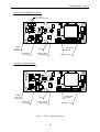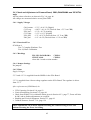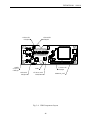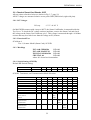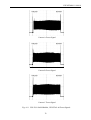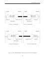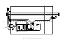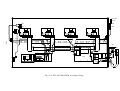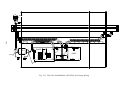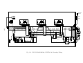
1
Wide Format Scanner
Technical Service Manual
FSC x040 CHROMA, FSC x050 MAGNUM,
FSS 225x PANORAMA, and CRYSTAL 40
FSF/TSM/001 (1.5c)
Part Number 6799A127
1
DOCUMENT REVISION RECORD
2
LIST OF DOCUMENTS
FSF MAINTENANCE MANUAL
3
FSC x040 CHROMA, FSC x050 MAGNUM,
FSS 225x PANORAMA, and CRYSTAL 40
4
5
6
7
8
SPARE PARTS AND SERVICE ACCESSORIES
9
10
FSC x040 CHROMA, FSC x050 MAGNUM,
FSS 225x PANORAMA, and CRYSTAL 40
TECHNICAL SERVICE BULLETINS
FSF/TSM/001
Document Revision Record
REV.
DATE
CHANGED
BY
PAGES
AFFECTED
1.0
1.1
990927
991201
BN/LM
BN/LM
All
All
1.2
000614
BN/LM
All
1.3
1.4
000901
010919
BN/LM
BN/LM
All
All
1.5
1.5a
1.5b
1.5c
020927
030623
030922
050607
BN/LM
LM
LM
LM
All
DRR
BRIEF DESCRIPTION OF CHANGE
Original Issue of Document
FSF/MTM/001 (1.1)
SOF/PLS/007 (1.2)
FSF/MTM/001 (1.2)
SOF/PLS/007 (1.3)
SOF/PLS/007 (1.4)
FSF/MTM/001 (1.3)
SOF/PLS/007 (1.5)
SOF/PLS/007 (1.6)
FSF/TSB/001 added
FSF/TSB/002 added
Document Revision Record added
FSF/TSB/003 added
1
FSF/TSM/001 030922
List of Documents:
FSF/MTM/001 (1.3)
FSF Maintenance Manual
FSC x040 CHROMA, FSC x050 MAGNUM,
FSS 225x PANORAMA, and CRYSTAL 40
SOF/PLS/007
(1.6)
Spare Part and Service Accessories
FSC x040 CHROMA, FSC x050 MAGNUM,
FSS 225x PANORAMA, and CRYSTAL 40
FSF/TSB/001
FSF/TSB/002
(1.0)
(1.0)
Ageing of Fluorescent Lamps
Cracking solder joints on SMPS
TITLE:
FSF MAINTENANCE MANUAL
FSC x040 CHROMA and FSC x050 MAGNUM
FSS 225x PANORAMA and CRYSTAL 40
DOC. NO.:
FSF/MTM/001
PREPARED BY:
BN/LM
AUTHORIZED:
JR
DISTRIBUTION:
Tegningsarkiv, Svendborg
PT, Svendborg
DD
ISSUE REVISION:
DATE:
(1)
(1)
(1)
1.3
2001-09-19
A P P R O V E D B Y:
AUTHORITY
DATE
SIGNATURE
This document is the property of Contex A/S. The data contained herein, in whole or in
part, may not be duplicated, used or disclosed outside the Recipient for any purpose other
than to conduct technical evaluation. This restriction does not limit the Recipients right to
use information contained in the data if it is obtained from another source without
restriction..
FSF/MTM/001
Document Revision Record
DRR
REV.
DATE
CHANGED
BY
PAGES
AFFECTED
BRIEF DESCRIPTION OF CHANGE
1.0
990927
BN
All
Original issue of document
1.1
991201
BN
All
CHROMA variants added
Definition of Board Revision changed
to reflect functionality only (Sec. 3.1).
1.2
0000614
BN
All
PANORAMA variants added
Changed description of Updating of
Light Profiles, 2.5.3. Minor changes
in 8.1 and 8.2
1.3
010919
BN
All
CRYSTAL 40 added.
Test 9 of SCANtest 6, rel. 1 supports
Software Oscilloscope.
2
FSF/MTM/001 010919
Table of Contents
LIST OF FIGURES ..................................................................................................................................7
1.
INTRODUCTION ....................................................................................................................................9
2.
GENERAL DESCRIPTION ..................................................................................................................10
2.1
2.2
2.3
2.4
2.4.1
2.4.2
2.4.3
2.5
2.5.1
2.5.2
2.5.3
2.5.4
2.6
2.6.1
2.6.2
2.6.3
2.7
2.7.1
2.7.2
2.7.3
2.7.4
2.7.5
2.8
2.9
FSC X040 CHROMA AND FSC X050 MAGNUM COLOR SCANNERS ....................................................10
FSS225X PANORAMA AND CRYSTAL 40 MONOCHROME SCANNERS .................................................14
SMPS, SWITCH MODE POWER SUPPLY .....................................................................................................16
LMD, MOTOR AND LAMP DRIVER BOARD ................................................................................................16
Lamp Driver.........................................................................................................................................16
Stepper Motor Control.........................................................................................................................16
Automatic Voltage Switching...............................................................................................................16
CBC, CAMERA BOARD (MAGNUM AND CHROMA ONLY) ....................................................................18
Color CCD Chip ..................................................................................................................................18
Wolfson Scanner Processor .................................................................................................................18
Automatic Updating of Light Profile Correction and Stitching...........................................................19
Line RAM.............................................................................................................................................20
CBB, CAMERA BOARD (PANORAMA AND CRYSTAL ONLY) ...............................................................22
Wolfson Scanner Processor .................................................................................................................22
Automatic Updating of Light Profile Correction and Stitching...........................................................23
Line RAM.............................................................................................................................................23
SUA, SCANNER UNIT ................................................................................................................................25
Processor Module................................................................................................................................25
Data Acquisition Module.....................................................................................................................25
Double Buffer Module .........................................................................................................................26
Stepper Motor Pulse Generator...........................................................................................................27
SCSI Interface......................................................................................................................................27
SCR, SMART CARD READER .....................................................................................................................29
SKC, OPERATOR PANEL............................................................................................................................31
3.
ELECTRICAL CHECK AND ADJUSTMENTS ................................................................................33
3.1
3.2
3.2.1
3.3
3.3.1
3.3.2
3.3.3
3.3.4
3.3.5
3.3.6
3.3.7
3.4
3.4.1
3.4.2
3.4.3
3.4.4
3.4.5
3.4.6
3.4.7
3.5
3.5.1
3.5.2
3.5.3
MARKING CODES FOR CIRCUIT BOARDS AND PROGRAMMED DEVICES .....................................................33
DOWNLOADING SCANNER FIRMWARE .......................................................................................................33
Erase and Restore Parameter Blocks ..................................................................................................34
CHECK AND ADJUSTMENT OF THE SWITCH MODE POWER SUPPLY, SMPS................................................35
AC Voltages .........................................................................................................................................35
DC Voltages.........................................................................................................................................35
Adjustments..........................................................................................................................................35
Fuses....................................................................................................................................................36
Markings..............................................................................................................................................36
Jumper Settings....................................................................................................................................36
Hints.....................................................................................................................................................36
CHECK AND ADJUSTMENT OF LAMP AND MOTOR DRIVER BOARD, LMD .................................................38
DC Voltages.........................................................................................................................................38
Lamp-Driver Adjustment .....................................................................................................................38
Stepper Motor Reference Voltages ......................................................................................................39
Fuses....................................................................................................................................................39
Markings..............................................................................................................................................39
Jumper Settings....................................................................................................................................40
Hints.....................................................................................................................................................40
CHECK AND ADJUSTMENT OF CAMERA BOARD, CBC (MAGNUM AND CHROMA ONLY) .....................42
Supply Voltages ...................................................................................................................................42
Adjustments..........................................................................................................................................42
Functional Test ....................................................................................................................................42
3
FSF/MTM/001 010919
3.5.4
Markings..............................................................................................................................................42
3.5.5
Jumper Settings....................................................................................................................................42
3.5.6
Hints.....................................................................................................................................................42
3.6
CHECK AND ADJUSTMENT OF CAMERA BOARD, CBB (PANORAMA AND CRYSTAL ONLY) ................45
3.6.1
Supply Voltages ...................................................................................................................................45
3.6.2
Functional Test ....................................................................................................................................45
3.6.3
Markings..............................................................................................................................................45
3.6.4
Jumper Settings....................................................................................................................................45
3.6.5
Hints.....................................................................................................................................................45
3.7
CHECK OF SCANNER UNIT, SUA ...............................................................................................................47
3.7.1
Supply Voltages ...................................................................................................................................47
3.7.2
Adjustments..........................................................................................................................................47
3.7.3
Functional Test ....................................................................................................................................47
3.7.4
Markings..............................................................................................................................................47
3.7.5
Switch Settings (Download Control Switches).....................................................................................47
3.7.6
Jumper Settings....................................................................................................................................48
3.7.7
Signal LEDs on the SUA-Board ..........................................................................................................48
3.7.8
Hints.....................................................................................................................................................48
3.8
CHECK OF OPERATOR PANEL, SKC...........................................................................................................50
3.8.1
Supply Voltages ...................................................................................................................................50
3.8.2
Functional Test ....................................................................................................................................50
3.8.3
Markings..............................................................................................................................................50
3.8.4
Switch Setting (Scanner ID).................................................................................................................50
3.9
CHECK OF SMART CARD READER, SCR ....................................................................................................52
3.9.1
DC Voltages.........................................................................................................................................52
3.9.2
Functional Test ....................................................................................................................................52
3.9.3
Markings..............................................................................................................................................52
3.9.4
Switch Setting (SCSI ID)......................................................................................................................52
3.9.5
Signal LED on the SCR-Board ............................................................................................................53
3.9.6
Hints.....................................................................................................................................................53
3.10
CHECK OF LAMP SENSOR BOARD, OSB ....................................................................................................55
3.10.1 Functional Test ....................................................................................................................................55
3.10.2 Markings..............................................................................................................................................55
3.11
CHECK OF OPTOINTERRUPTER BOARD, OIBA...........................................................................................55
3.11.1 Functional Test ....................................................................................................................................55
3.11.2 Markings..............................................................................................................................................55
3.12
ADJUSTMENT OF ORIGINAL SENSORS ........................................................................................................57
3.12.1 Adjustment of Switch Point ..................................................................................................................57
3.12.2 Functional Test ....................................................................................................................................57
3.12.3 Hints.....................................................................................................................................................57
3.13
CHECK OF MEDIA THICKNESS DETECTOR .................................................................................................59
3.13.1 Functional Test ....................................................................................................................................59
4.
CCD-CAMERAS....................................................................................................................................60
4.1
DESCRIPTION OF CCD-CAMERAS ..............................................................................................................60
4.2
CCD-CAMERA ADJUSTMENT ....................................................................................................................64
4.2.1
Light Profiles .......................................................................................................................................64
4.2.2
Focus ...................................................................................................................................................72
4.2.3
Scan-Width...........................................................................................................................................77
4.2.4
CCD-Centering....................................................................................................................................83
4.2.5
Vertical Positioning .............................................................................................................................84
4.2.6
Final Check..........................................................................................................................................85
5.
STITCHING AND VERTICAL ALIGNMENT ..................................................................................94
5.1
PRINCIPLE OF STITCHING ...........................................................................................................................94
5.2
STITCHING ADJUSTMENT ...........................................................................................................................94
5.2.1
Vertical Alignment ...............................................................................................................................95
5.3
STITCHING AND VERTICAL ALIGNMENT.....................................................................................................99
5.3.1
FSC x040 CHROMA............................................................................................................................99
4
FSF/MTM/001 010919
5.3.2
5.3.3
FSC x050 MAGNUM .........................................................................................................................102
FSS 225x PANORAMA and CRYSTAL 40 .........................................................................................105
6.
MAINTENANCE CHECK OF CCD-CAMERA ADJUSTMENTS ................................................108
6.1
6.2
6.3
LIGHT PROFILE ........................................................................................................................................108
FOCUS .....................................................................................................................................................116
SCAN-WIDTH, CCD-CENTERING AND VERTICAL POSITIONING ...............................................................120
7.
GENERAL MAINTENANCE .............................................................................................................133
7.1
STEP BY STEP PROCEDURE FOR GENERAL MAINTENANCE ......................................................................133
7.1.1
Remove Top Cover.............................................................................................................................133
7.1.2
Cleaning of the Scanning Area ..........................................................................................................133
7.1.3
Fluorescent Lamps.............................................................................................................................133
7.1.4
Check Lamp Driver Adjustment.........................................................................................................133
7.1.5
Check CCD-Camera Adjustment .......................................................................................................134
7.1.6
Readjustment of CCD-Cameras.........................................................................................................134
7.1.7
Mount Top Cover...............................................................................................................................134
7.1.8
Check Stitching and Vertical Alignment ............................................................................................134
7.1.9
Calibrate Scanner..............................................................................................................................134
8.
TROUBLESHOOTING .......................................................................................................................138
8.1
POWER-ON SELF-TEST ............................................................................................................................138
8.2
ERROR CODES .........................................................................................................................................138
8.2.1
Error Codes displayed on the Operator Panel ..................................................................................138
8.2.2
Error Codes displayed on the PC Screen ..........................................................................................139
8.3
TROUBLESHOOTING HINTS ......................................................................................................................142
9.
DISASSEMBLY AND ASSEMBLY ...................................................................................................145
9.1
9.1.1
9.1.2
9.2
9.3
9.4
9.5
9.6
9.7
9.8
9.9
9.10
TOP COVER WITH FRONT PROFILE ...........................................................................................................145
Front Profile ......................................................................................................................................145
Smart Card Reader on MAGNUM, up to s/n 00275 ..........................................................................145
END COVERS ...........................................................................................................................................146
REAR COVER ...........................................................................................................................................146
BOTTOM PLATE .......................................................................................................................................146
TOP PROFILE (LID) ..................................................................................................................................146
GLASS PLATE ..........................................................................................................................................146
ENTRY ROLLER SHIELD ...........................................................................................................................146
EXIT ROLLER SHIELD ..............................................................................................................................147
MIRROR CHASSIS ....................................................................................................................................147
REFLECTOR ASSEMBLY ...........................................................................................................................148
10.
REPLACEMENT OF PARTS.............................................................................................................149
10.1
10.2
10.3
10.4
10.5
10.6
10.7
10.8
10.9
FEED ROLLER SHAFT ...............................................................................................................................149
ORIGINAL SENSOR ACTUATORS...............................................................................................................150
STITCHING WIRE .....................................................................................................................................150
FLUORESCENT LAMPS .............................................................................................................................150
STEPPER MOTOR .....................................................................................................................................151
LAMP SENSOR BOARD, OSB ...................................................................................................................151
DUST FILTER ON FAN ..............................................................................................................................152
WHITE BACKGROUND PLATE ..................................................................................................................152
SLIDER FOR MEDIA THICKNESS ADJUSTMENT .........................................................................................152
11.
SCANTEST 4 ........................................................................................................................................156
11.1.1
11.1.2
11.1.3
11.1.4
11.1.5
11.1.6
Test 1,
Test 2,
Test 3,
Test 4,
Test 5,
Test 6,
Scanner Information .............................................................................................................157
LED Test ...............................................................................................................................157
Key Test.................................................................................................................................157
Original-Sensor Test .............................................................................................................157
Lamp Test..............................................................................................................................157
Motor Test .............................................................................................................................158
5
FSF/MTM/001 010919
11.1.7
11.1.8
11.1.9
11.1.10
11.1.11
11.1.12
11.1.13
11.1.14
11.1.15
Test 7, Complete Hardware Test ......................................................................................................158
Test 9, Camera Adjustment...............................................................................................................158
Test 10, Check Camera Adjustment ..................................................................................................158
Test 11, Stitching and Vertical Alignment ........................................................................................159
Test 12, Adjustment of Y-Axis Scaling ..............................................................................................159
Test 13, Switch Scanner to Test Mode ..............................................................................................159
Test 16, Basic Calibration ................................................................................................................159
Test 20, Noise Test ............................................................................................................................160
Test 21, SCANdump ..........................................................................................................................162
12.
WIRING DIAGRAMS .........................................................................................................................163
13.
SPECIAL SERVICE TOOLS..............................................................................................................170
6
FSF/MTM/001 010919
List of Figures
FIG. 2-1 FSC X040 CHROMA BLOCK DIAGRAM .......................................................................................12
FIG. 2-2 FSC X050 MAGNUM BLOCK DIAGRAM ......................................................................................13
FIG. 2-3 FSS 225X PANORAMA, CRYSTAL 40 BLOCK DIAGRAM .........................................................15
FIG. 2-4 LMD BLOCK DIAGRAM....................................................................................................................17
FIG. 2-5 CBC BLOCK DIAGRAM ....................................................................................................................21
FIG. 2-6 CBB BLOCK DIAGRAM ....................................................................................................................24
FIG. 2-7 SUA BLOCK DIAGRAM ....................................................................................................................28
FIG. 2-8 SCR BLOCK DIAGRAM.....................................................................................................................30
FIG. 2-9 SKC BLOCK DIAGRAM.....................................................................................................................32
FIG. 3-1 SMPS TEST POINTS...........................................................................................................................37
FIG. 3-2 LMD COMPONENT LAYOUT...........................................................................................................41
FIG. 3-3 CBC COMPONENT LAYOUT............................................................................................................44
FIG. 3-4 CBB COMPONENT LAYOUT............................................................................................................46
FIG. 3-5 SUA COMPONENT LAYOUT............................................................................................................49
FIG. 3-6 SKC COMPONENT LAYOUT ............................................................................................................51
FIG. 3-7 SCR COMPONENT LAYOUT ............................................................................................................54
FIG. 3-8 OSB COMPONENT LAYOUT............................................................................................................56
FIG. 3-9 OIBA COMPONENT LAYOUT..........................................................................................................56
FIG. 3-10 ADJUSTMENT OF ORIGINAL-SENSORS.......................................................................................58
FIG. 4-1 CCD-CAMERA, SIDE VIEW ...............................................................................................................62
FIG. 4-2 OSCILLOSCOPE IMAGES FOR CAMERA ADJUSTMENT .............................................................63
FIG. 4-3 FSC X040 CHROMA LIGHT PROFILES, UNCORRECTED .............................................................66
FIG. 4-4 FSC X040 CHROMA LIGHT PROFILES, CORRECTED...................................................................67
FIG. 4-5 FSC X050 MAGNUM LIGHT PROFILES, UNCORRECTED............................................................68
FIG. 4-6 FSC X050 MAGNUM LIGHT PROFILES, CORRECTED..................................................................69
FIG. 4-7 FSS 225X PANORAMA, CRYSTAL 40, LIGHT PROFILES, UNCORRECTED ..............................70
FIG. 4-8 FSS 225X PANORAMA, CRYSTAL 40, LIGHT PROFILES, CORRECTED....................................71
FIG. 4-9 FSC X040 CHROMA FOCUS SIGNALS .............................................................................................74
FIG. 4-10 FSC X050 MAGNUM FOCUS SIGNALS..........................................................................................75
FIG. 4-11 FSS 225X PANORAMA, CRYSTAL 40, FOCUS SIGNALS ............................................................76
FIG. 4-12 FSC X040 CHROMA, SCAN-WIDTH ...............................................................................................79
FIG. 4-13 FSC X050 MAGNUM, SCAN-WIDTH (1) ........................................................................................80
FIG. 4-14 FSC X050 MAGNUM, SCAN-WIDTH (2) ........................................................................................81
FIG. 4-15 FSS 225X PANORAMA, CRYSTAL 40, SCAN-WIDTH..................................................................82
FIG. 4-16 FSC X040 CHROMA, CCD-CENTERING AND VERTICAL POSITIONING ................................86
FIG. 4-17 FSC X050 MAGNUM, CCD-CENTERING AND VERTICAL POSITIONING (1) .........................87
FIG. 4-18 FSC X050 MAGNUM, CCD-CENTERING AND VERTICAL POSITIONING (2) ........................88
FIG. 4-19 FSS 225X PANORAMA, CRYSTAL 40, CCD-CENTERING AND VERTICAL POSITIONING ..89
FIG. 4-20 TEST POINTS FOR CAMERA ADJUSTMENTS .............................................................................90
FIG. 4-21 CCD-CAMERA, TOP VIEW ..............................................................................................................91
FIG. 4-22 OPTICAL ADJUSTMENT PATTERNS...............................................................................................92
FIG. 4-23 FOCUS PATTERN..............................................................................................................................93
FIG. 5-1 PRINCIPLE OF STITCHING ...............................................................................................................96
FIG. 5-2 STITCHING WIRE MOUNTING.........................................................................................................97
FIG. 5-3 STITCHING ADJUSTMENT CHART .................................................................................................98
FIG. 5-4 FSC X040 CHROMA, STITCHING IMAGES ..................................................................................101
FIG. 5-5 FSC X050 MAGNUM, STITCHING IMAGES .................................................................................104
FIG. 5-6 FSS 225X PANORAMA, CRYSTAL 40, STITCHING IMAGES ....................................................107
FIG. 6-1 FSC X040 CHROMA, LIGHT PROFILES UNCORRECTED (WBP)..............................................110
FIG. 6-2 FSC X040 CHROMA, LIGHT PROFILES CORRECTED (WBP) ...................................................111
FIG. 6-3 FSC X040 CHROMA, LIGHT PROFILES CORRECTED (BCS).....................................................111
FIG. 6-4 FSC X050 MAGNUM, LIGHT PROFILES UNCORRECTED (WBP) ............................................112
FIG. 6-5 FSC X050 MAGNUM, LIGHT PROFILES CORRECTED (WBP) ..................................................113
FIG. 6-6 FSC X050 MAGNUM, LIGHT PROFILES CORRECTED (BCS) ...................................................113
FIG. 6-7 FSS 225X PANORAMA, CRYSTAL 40, LIGHT PROFILES UNCORRECTED (WBP)................114
FIG. 6-8 FSS 225X PANORAMA, CRYSTAL 40, LIGHT PROFILES CORRECTED (WBP)......................115
7
FSF/MTM/001 010919
FIG. 6-9 FSS 225X PANORAMA, CRYSTAL 40, LIGHT PROFILES CORRECTED (BCS).......................115
FIG. 6-10 FSC X040 CHROMA, FOCUS SIGNALS UNCORRECTED..........................................................117
FIG. 6-11 FSC X040 CHROMA, FOCUS SIGNALS CORRECTED ...............................................................117
FIG. 6-12 FSC X050 MAGNUM, FOCUS SIGNALS UNCORRECTED.........................................................118
FIG. 6-13 FSC X050 MAGNUM, FOCUS SIGNALS CORRECTED ..............................................................118
FIG. 6-14 FSS 225X PANORAMA, CRYSTAL 40, FOCUS SIGNALS UNCORRECTED ............................119
FIG. 6-15 FSS 225X PANORAMA, CRYSTAL 40, FOCUS SIGNALS CORRECTED..................................119
FIG. 6-16 FSC X040 CHROMA, CAMERA A, SCANLINE START...............................................................123
FIG. 6-17 FSC X040 CHROMA, CAMERA A, SCANLINE END ...................................................................123
FIG. 6-18 FSC X040 CHROMA, CAMERA B, SCANLINE START...............................................................124
FIG. 6-19 FSC X040 CHROMA, CAMERA B, SCANLINE END ...................................................................124
FIG. 6-20 FSC X040 CHROMA, CAMERA C, SCANLINE START...............................................................125
FIG. 6-21 FSC X040 CHROMA, CAMERA C, SCANLINE END ...................................................................125
FIG. 6-22 FSC X050 MAGNUM, CAMERA A, SCANLINE START..............................................................126
FIG. 6-23 FSC X050 MAGNUM, CAMERA A, SCANLINE END ..................................................................126
FIG. 6-24 FSC X050 MAGNUM, CAMERA B, SCANLINE START..............................................................127
FIG. 6-25 FSC X050 MAGNUM, CAMERA B, SCANLINE END ..................................................................127
FIG. 6-26 FSC X050 MAGNUM, CAMERA C, SCANLINE START..............................................................128
FIG. 6-27 FSC X050 MAGNUM, CAMERA C, SCANLINE END ..................................................................128
FIG. 6-28 FSC X050 MAGNUM, CAMERA D, SCANLINE START .............................................................129
FIG. 6-29 FSC X050 MAGNUM, CAMERA D, SCANLINE END..................................................................129
FIG. 6-30 FSS 225X PANORAMA, CRYSTAL 40, CAMERA A, SCANLINE START .................................130
FIG. 6-31 FSS 225X PANORAMA, CRYSTAL 40, CAMERA A, SCANLINE END .....................................130
FIG. 6-32 FSS 225X PANORAMA, CRYSTAL 40, CAMERA B, SCANLINE START .................................131
FIG. 6-33 FSS 225X PANORAMA, CRYSTAL 40, CAMERA B, SCANLINE END .....................................131
FIG. 6-34 FSS 225X PANORAMA, CRYSTAL 40, CAMERA C, SCANLINE START .................................132
FIG. 6-35 FSS 225X PANORAMA, CRYSTAL 40, CAMERA C, SCANLINE END......................................132
FIG. 7-1 BASIC-CALIBRATION SHEET ........................................................................................................135
FIG. 7-2 IT8 COLOR CALIBRATION SHEET, CHROMA.............................................................................136
FIG. 7-3 IT8 COLOR CALIBRATION SHEET, MAGNUM............................................................................137
FIG. 10-1 TRANSMISSION ..............................................................................................................................153
FIG. 10-2 DRIVE-BELT TIGHTENER.............................................................................................................154
FIG. 10-3 SCANNER CROSS SECTION..........................................................................................................155
FIG. 11-1 NOISE TEST, EXAMPLE.................................................................................................................161
FIG. 12-1 FSC X040 CHROMA PRIMARY WIRING.....................................................................................164
FIG. 12-2 FSC X040 CHROMA SECONDARY WIRING ..............................................................................165
FIG. 12-3 FSC X050 MAGNUM PRIMARY WIRING ...................................................................................166
FIG. 12-4 FSC X050 MAGNUM SECONDARY WIRING .............................................................................167
FIG. 12-5 FSS 225X PANORAMA, CRYSTAL 40, PRIMARY WIRING......................................................168
FIG. 12-6 FSS 225X PANORAMA, CRYSTAL 40, SECONDARY WIRING................................................169
8
FSF/MTM/001 010919
1. Introduction
The purpose of this Maintenance Manual is to provide technical information to support boardlevel troubleshooting and maintenance of the Wide Format Scanners:
FSC x050 MAGNUM (generic model designation FA67A)
FSC x040 CHROMA (generic model designation FB67A)
FSS 225x PANORAMA alias PANORAMA 50 (generic model designation FC67A)
CRYSTAL 40 (generic model designation FD67A)
Chapter 2 contains a general technical description based on block diagrams.
Chapter 3 describes Electrical Check and Adjustments including jumper and switch settings.
Chapter 4 contains a general description of the Optical System and the CCD-Camera
Adjustments.
Chapter 5 describes Stitching and Vertical Alignment.
Chapter 6 contains a set of screen images to be used for Maintenance Check of the CCDCamera adjustment.
Chapter 7 describes General Maintenance.
Chapter 8 contains a list of Error Codes and gives some hints on troubleshooting.
Chapter 9 describes Disassembly and Assembly procedures.
Chapter 10 provides a guide for replacement of parts for which the procedure is not obvious.
Chapter 11 describes the scanner test program, SCANtest 4.
SCANtest 6, rel. 1 and firmware rel. 0031 or later supports “Software Oscilloscope” in Test 9.
Chapter 12 contains Wiring Diagrams.
Chapter 13 contains a list of Special Service Tools.
9
FSF/MTM/001 010919
2. General Description
The Wide Format Color and Monochrome Scanners, which are marketed under the following
product names:
FSC3050 MAGNUM
FSC6050 MAGNUM
FSC8050 MAGNUM
FSC3040 CHROMA
FSC6040 CHROMA
FSC8040 CHROMA
FSS2250 PANORAMA alias PANORAMA 50
FSS2251 PANORAMA alias PANORAMA 50 PLUS
CRYSTAL 40
CRYSTAL 40 PLUS
and the modules:
SMPS, Switch Mode Power Supply
LMDA, Lamp and Motor Driver Board
CBCA, Camera Board (MAGNUM, CHROMA)
CBBB, Camera Board (PANORAMA, CRYSTAL)
SUAB, Scanner Unit (MAGNUM, CHROMA)
SUAC, Scanner Unit (PANORAMA, CRYSTAL)
SKCA, Operator Panel Board
SCRA, Smart Card Reader
are described at block-diagram level in Sections 2.1 through 2.9.
For installation of the ASPI compatible SCSI Adapter that is included with the Interface Kit
for PC, refer to the Operator’s Guide for the Wide Format Color Scanners and the User’s
Guide for the WIDEimage scanning application.
2.1 FSC x040 CHROMA and FSC x050 MAGNUM Color Scanners
The Block Diagrams are shown in:
Fig. 2-1 FSC x040 CHROMA Block Diagram, page 12
Fig. 2-2 FSC x050 MAGNUM Block Diagram, page13
The functionality of the CHROMA and MAGNUM Wide Format Color Scanners, such as
•
•
•
max. image resolution
scanning speed
digital image processing
10
FSF/MTM/001 010919
depends on a Smart Card located behind the Model Streamer on the Front Profile of the
scanner.
The CHROMA and MAGNUM scanner range consists of:
Generic
Model
Product Name
(Smart Card)
FB67A
FA67A
-
FSC3040 CHROMA
FSC6040 CHROMA
FSC8040 CHROMA
FSC3050 MAGNUM
FSC6050 MAGNUM
FSC8050 MAGNUM
Scan
Width
(inches)
40
40
40
50
50
50
No. of
Cameras
Optical Resolution
(dpi)
3
3
3
4
4
4
390
390
390
400
400
400
Level of
Functionality
(Smart Card)
Basic
Medium
High
Basic
Medium
High
The scan-area is illuminated by two white fluorescent lamps. The light output from the lamps
is stabilized by feedback to the lamp power supply board (LMD).
Each CCD-Camera in the scanner contains one 5363 x 3 pixel color CCD. The output signals
from the CCDs are Light Profile Corrected at pixel level.
In order to stitch (bring together) scanlines from adjacent cameras, the fields of vision of the
CCD-Cameras overlap slightly and a thin, black wire placed within the overlapped fields of
vision marks the virtual end, respectively start, of adjacent scanlines.
The scanlines from the individual cameras are mechanically aligned in the vertical direction.
All scanning and image processing functions are contained on only two boards, the Camera
Board (CBC) and the Scanner Unit Board (SUAB).
The scanner has one dual SCSI Port (SCAN SCSI 0-A and 0-B) used for normal Scan-to-File
operations, and one single SCSI Port (COPY SCAN 1) used when a separate Copy-PC
configuration is attached simultaneously with a Scan-to-File PC.
The interface is SCSI-3 with a transfer rate up to 20 MB/s.
11
ORIGINAL
SCAN LIN E
OSBC
SENSORS
F LU ORESCENT LAMP
OIBA
THICKNESS
SENSOR
F LU ORESCENT LAMP
OSBC
OIBA
OPERATOR
MIRRORS
PANEL
SKC
CAMERA C
CAMERA B
CBC
CBC
CAMERA A
CBC
12
FEED MOTOR
LMD
LAMP AND MOTOR
D RIVER BOARD
FAN
SUAB
SCANNER UNIT
SCSI ID
SWITCH
RFI
Fig. 2-1 FSC x040 CHROMA Block Diagram
SCR
SMART
CARD
SIB
FSF/MTM/001 010919
SMPS
SWITCH MOD E
POWER SUPPLY
ORIGINAL
SCAN LIN E
OSBC
SENSORS
FLUORESCENT LAMP
OIBA
THICKN ESS
SENSOR
FLUORESCENT LAMP
OSBC
OIBA
OPERATOR
MIRRORS
PANEL
SKC
CAMERA D
CAMERA C
CBC
CBC
CAMERA B
CBC
CAMERA A
CBC
13
FEED MOTOR
LMD
LAMP AND MOTOR
D RIVER BOARD
FAN
SUAB
SCANNER UNIT
SCSI ID
SWITC H
RFI
Fig. 2-2 FSC x050 MAGNUM Block Diagram
SCR
SMART
CARD
SIB
FSF/MTM/001 010919
SMPS
SWITCH MOD E
POWER SUPPLY
FSF/MTM/001 010919
2.2 FSS225x PANORAMA and CRYSTAL 40 Monochrome Scanners
The Block Diagram is shown in:
Fig. 2-3 FSS 225x PANORAMA, CRYSTAL 40 Block Diagram, page 15
The functionality of the PANORAMA and CRYSTAL Wide Format Monochrome Scanners,
such as
•
•
•
max. image resolution
scanning speed
digital image processing
depends on a Smart Card located behind the Model Streamer on the Front Profile of the
scanner.
The PANORAMA and CRYSTAL scanner range consists of:
Generic
Model
Product Name
(Smart Card)
FC67A
FD67A
-
FSS2250 PANORAMA
FSS2251 PANORAMA
CRYSTAL 40
CRYSTAL 40 PLUS
Scan
Width
(inches)
50
50
40
40
No. of
Cameras
Optical Resolution
(dpi)
3
3
3
3
461
461
461
461
Level of
Functionality
(Smart Card)
Basic (BASIC)
High (PLUS)
Basic (BASIC)
High (PLUS)
The scan-area is illuminated by two white fluorescent lamps. The light output from the lamps
is stabilized by feedback to the lamp power supply board (LMD).
Each CCD-Camera in the scanner contains one 7926 pixel CCD. The output signals from the
CCDs are Light Profile Corrected at pixel level.
In order to stitch (bring together) scanlines from adjacent cameras, the fields of vision of the
CCD-Cameras overlap slightly and a thin, black wire placed within the overlapped fields of
vision marks the virtual end, respectively start, of adjacent scanlines.
The scanlines from the individual cameras are mechanically aligned in the vertical direction.
All scanning and image processing functions are contained on only two boards, the Camera
Board (CBB) and the Scanner Unit Board (SUAC).
The scanner has one dual SCSI Port (SCAN SCSI 0-A and 0-B) used for normal Scan-to-File
operations, and one single SCSI Port (COPY SCAN 1) used when a separate Copy-PC
configuration is attached simultaneously with a Scan-to-File PC.
The interface is SCSI-3 with a transfer rate up to 20 MB/s.
14
ORIGINAL
SCAN LIN E
OSBC
SENSORS
FLUORESCENT LAMP
OIBA
THICKN ESS
SENSOR
FLUORESCENT LAMP
OSBC
OIBA
OPERATOR
MIRRORS
PANEL
SKC
CAMERA C
CAMERA B
CBB
CBB
CAMERA A
CBB
15
FEED MOTOR
LMD
LAMP AND MOTOR
D RIVER BOARD
FAN
SUAC
SCANNER UNIT
SCSI ID
SWITC H
RFI
SCR
SMART
CARD
Fig. 2-3 FSS 225x PANORAMA, CRYSTAL 40 Block Diagram
SIB
FSF/MTM/001 010919
SMPS
SWITCH MOD E
POWER SUPPLY
FSF/MTM/001 010919
2.3 SMPS, Switch Mode Power Supply
The SMPS is a standard Switched Mode Power Supply containing:
Primary Fuse
Rectifiers and Filter Capacitors
Switch Mode Voltage Regulators
Voltage Outputs
+5.3 V which is used as supply for the LMD-, SUA-, and CBC- Boards
+12 V which is used as supply for the LMD-, SUA-, and CBC- Boards
-12 V which is used on the LMD-Board
+24 V which is used on the LMD-Board (Stepper Motor supply)
2.4 LMD, Motor and Lamp Driver Board
The LMD Block Diagram is shown in Fig. 2-4, page 17.
The LMD-Board contains the following functional circuits:
Interconnection between Power Inlet and SMPS
Primary fuse for Lamp Driver
Rectifiers and Filter Capacitors for the Lamp Drivers
Lamp Driver Control Circuits
Stepper-Motor Control and Drive Circuit
Automatic Voltage Switching between 100-120 V and 220-240 V
2.4.1 Lamp Driver
Each of the two Lamp Driver Circuits uses a SMPS Controller to drive the Power FETs which
drive the lamps.
The light outputs from the two lamps are stabilized by feedback from two OSB-Boards that
are located close to the lamps at the ‘Power Inlet End’ of the scanner.
2.4.2 Stepper Motor Control
The stepper motor is driven in switched, current controlled mode. Each winding of the twophase bipolar stepper motor is driven by a full-bridge driver. The drive signals for the stepper
motor are generated by two EPROMs which are controlled by an up-down counter. The digital
output from the EPROMs are converted to analog signals which control the stepper motor
phase currents. The controller can operate with up to 64 micro-steps. The number of microsteps and the direction of rotation are controlled by the processor on the SUA-Board.
2.4.3 Automatic Voltage Switching
As the scanner is switched ON, the LMD-Board adapts automatically to either the low supply
voltage range, 100-120 V, or the high supply voltage range, 220-240 V according to the actual
mains voltage.
The Automatic Voltage Switching circuit consists of a triac and a controller circuit.
16
MAINS VOLTAGE AREA
J3
F1
LINE
POWER
INLET
R ECTIFIER
WITH
AUTOMATIC
VOLTAGE
SWITCHING
NEUTRAL
NEUTRAL
TO
SMPS
+16 0V(UNREG)
TP1
NEUTRAL
TP2
LAMP
-16 0V(UNREG)
TP3
DRIVER
+ 160V
J5
5
1
-160V
LINE
P1
+5 V
VR EF
TP4
TR1
CONTROL
J7
1
5
2
1
REAR
+ 160V
J8
FRONT
P2
+5 V
LAMP
FRONT
8
4
LAMP
2
1
SENSOR
REAR
LAMP
J6
SENSOR
LAMP
4
8
DRIVER
-160V
VR EF
17
J2
6
5
4
3
2
1
+5 V
TP5
TR2
LAMP
CONTROL
+24 V
+12 V
+5 V
-12 V
SR1
A
J1
LAMPON
B
LAMPON
15
LEVEL
3, 4,7
CTRL(2: 0)
8
STEP
P3
EPROM
11
DI R
1,6
I1,I2
STEPPER
MOTOR
DRIVER
P4
COUNTER
SUA
J9
TP7
DAC
EPROM
DAC
TP8
CONTROL
5
I0
9,10 ,12,13 ,14
CIRCUIT
Fig. 2-4 LMD Block Diagram
1
2
3
4
STEPPER
MOTOR
FSF/MTM/001 010919
2
FSF/MTM/001 010919
2.5 CBC, Camera Board (MAGNUM and CHROMA only)
The CBC Block Diagram is shown in Fig. 2-5, page 21.
The CBC-Board contains:
Color CCD-Chip, 5363 x 3 pixels
CDS, Correlated Double Sampling Circuits
Two Wolfson Scanner Processors (one for odd and one for even numbered
pixels)
AMP RAM (Light Profile Correction)
Line RAM (delays for Color Alignment and RGB filters)
FPGA, controlling the Wolfson processors and interface to the SUA
Flat cable connector for image data, clock signals and supply voltages
2.5.1 Color CCD Chip
The CCD pixels are arranged in three lines, one for each of the colors Red, Green, and Blue.
The spacing between the lines on the CCD chip is 64 µm corresponding to 8 scanlines at
optical resolution.
The lines are covered by color filters and arranged as follows:
Upper line on the CCD:
Center line on the CCD:
Lower line on the CCD:
Red
Green
Blue
As the image is mirrored by the lens, the Blue line becomes the upper line when referred to
the original.
The outputs from the CCD are buffered by three emitter followers and next Correlated Double
Sampled to correct for thermal black-current in the CCDs.
2.5.2 Wolfson Scanner Processor
The outputs from the CDS are fed into the two Wolfson Scanner Processors (one for odd
and one for even numbered pixels) which contains the following signal conditioning
functions:
2.5.2.1 Gain and Offset Control
The level and offset of the RGB signals may vary from camera to camera, and each channel
has Gain and Offset control circuits to adjust the signal level and the signal offset to match the
input-signal range of the following AD-Converter.
The gain and offset parameters are adjusted by running Basic Calibration or WIDEimage,
Calibrate Scanner and then they are stored in the Flash Memory on the SUA-Board.
2.5.2.2 AD-Converters
The AD-Converters operate on the multiplexed analog RGB signals and convert these into 12bit digital signals.
18
FSF/MTM/001 010919
2.5.2.3 Light Profile Correction
The digitized image signals are passed through a Multiplier to compensate for Photo Response
Non Uniformity (PRNU) and uneven light distribution along the scanline, and to provide a
pre-defined White-Signal level for the later signal processing on the SUA-Board.
The Light Profile Correction of the scanner is based on two Light Profiles obtained during
Basic Calibration or WIDEimage, Calibrate Scanner:
•
•
High resolution Light Profile of Basic-Calibration Sheet (BCS, stored in Flash
Memory on the SUA-Board)
Filtered Light Profile of the White Background Plate in the scanner (WBP, stored
in Flash Memory on the SUA-Board)
and one Light Profile which is automatically being updated whenever the scanner is idle and
the Original Guide Plate is full down in Normal position:
•
Filtered Light Profile of the White Background Plate of the scanner (UPD, stored
in RAM on the CBC-Board)
The Light Profile Correction uses the high resolution Light Profile to correct for PRNU and to
provide a pre-defined White-Signal level. The difference between the two filtered Light
Profiles is used to correct for changes in light level and light distribution that may have
happened after the last Basic Calibration or WIDEimage, Calibrate Scanner.
2.5.3 Automatic Updating of Light Profile Correction and Stitching
The automatic updating of the Light Profile mentioned above as well as Stitching (see Sec.
5.1, page 94) is suspended in the following cases:
Power On Self Test:
•
If the scanner is switched ON with the Original Guide Plate placed in one of the Extended
Media Thickness positions.
•
If the scanner is switched ON with media in the scan-area (detected by the Original Entry
and Exit Sensors), the feed motor is started in an attempt to remove the media from the
scan-area.
If the attempt to clear the scan-area fails, the update of the Light Profile is suspended.
When the condition for suspension has been detected, the WAIT LED on the Operator Panel
begins to blink to alert the user that the automatic Light Profile Correction has been
suspended. After the cause of the suspension has been rectified, the WAIT LED stays ON
continuously until the Light Profile Correction has been completed successfully.
During Operation:
•
Whenever the Original Guide Plate is placed in one of its Extended Thickness positions.
•
When scanning continuously (f. ex. batch scanning or prescanning).
19
FSF/MTM/001 010919
The duration of the suspension of the automatic Light Profile Correction is monitored by an
update-timer (the timing of which depends on the time elapsed since power on).
When the update-timer times out, the WAIT LED on the Operator Panel begins to blink to
alert the user that the automatic Light Profile Correction has been suspended. After the cause
of the suspension has been rectified, the WAIT LED stays ON continuously until the Light
Profile Correction has been completed successfully.
2.5.4 Line RAM
The physical spacing between the three lines of pixels (R, G and B) on the CCD corresponds
to 8 scanlines at the optical resolution of the scanner.
The RGB data supplied to the Colorspace Converter on the SUA-Board must refer to the same
physical location on the original, that is, Blue must be delayed 16, and Green 8 scanlines to
coincide with Red at optical resolution.
When scanning at DPIs for which the physical offset between the pixel arrays (referred to the
original) does not correspond to an integer number of scanlines, interpolated color data are
used as input for the Colorspace Converter. As for example, at 425 DPI, Blue must be delayed
17 and Green 8½ (interpolation between scanline N–8 and scanline N–9) scanlines.
That is, in the MAGNUM scanner which has an optical resolution of 400 DPI:
At 400 DPI
N–16
N–8
N
the Blue component of scanline no.
the Green component of scanline no.
the Red component of scanline no.
At 425 DPI
N–17
N–8½
N
refers to the same physical location on the original drawing.
The required delays are obtained by temporarily storing the scanlines in large RAM line
buffers and the interpolation between the scanlines is done by the FPGA circuit on the CBCBoard.
20
J1
POWER SUPPLY
4.8V
Wolfson Scanner Controller
SAMPLING
CCD
ILX518
5363x3
PIXELS
CDS
GAIN
OFFSET
MUX
ADC
LP
CORR.
ODD PIXELS
21
CTRL. SIGNALS
SAMPLING
GAIN
OFFSET
MUX
ADC
LP
CORR.
5.3V
IMAGE DATA
CTRL. SIGNALS
AMP
RAM
Wolfson Scanner Controller
REG
FPGA
LINE
RAM
CONTROL SIGNALS
EVEN PIXELS
40 MHz
CLOCK
MULT IPLIER
10 MHz
BUFFER
CLOCK SIGNALS
TP
ANALOG_OUT
FSF/MTM/001 010919
Fig. 2-5 CBC Block Diagram
DAC
FSF/MTM/001 010919
2.6 CBB, Camera Board (PANORAMA and CRYSTAL only)
The CBB Block Diagram is shown in Fig. 2-6, page 24.
The CBB-Board contains:
Monochrome CCD-Chip, 7926 pixels
Two Wolfson Scanner Processors (one for odd and one for even numbered
pixels)
AMP RAM (Light Profile Correction)
Line RAM (Delay and Gray filter)
FPGA, controlling the Wolfson processors and interface to the SUA
Flat cable connector for image data, clock signals and supply voltages
2.6.1 Wolfson Scanner Processor
The outputs from the differential amplifiers are fed into the two Wolfson Scanner Processors
(one for odd and one for even numbered pixels) which contains the following signal
conditioning functions:
2.6.1.1 Gain and Offset Control
The level and offset of the video signals may vary from camera to camera, and each channel
has Gain and Offset control circuits to adjust the signal level and the signal offset to match the
input-signal range of the following AD-Converter.
The gain and offset parameters are adjusted by running Basic Calibration or WIDEimage,
Calibrate Scanner and then they are stored in the Flash Memory on the SUA-Board.
2.6.1.2 AD-Converters
The AD-Converters operate on the analog video signals and convert these into 12-bit digital
signals.
2.6.1.3 Light Profile Correction
The digitized image signals are passed through a Multiplier to compensate for Photo Response
Non Uniformity (PRNU) and uneven light distribution along the scanline, and to provide a
pre-defined White-Signal level for the later signal processing on the SUA-Board.
The Light Profile Correction of the scanner is based on two Light Profiles obtained during
Basic Calibration or WIDEimage, Calibrate Scanner:
•
•
High resolution Light Profile of Basic-Calibration Sheet (BCS, stored in Flash
Memory on the SUA-Board)
Filtered Light Profile of the White Background Plate in the scanner (WBP, stored
in Flash Memory on the SUA-Board)
and one Light Profile which is automatically being updated whenever the scanner is idle and
the Original Guide Plate is full down in Normal position:
•
Filtered Light Profile of the White Background Plate of the scanner (UPD, stored
in RAM on the CBB-Board)
22
FSF/MTM/001 010919
The Light Profile Correction uses the high resolution Light Profile to correct for PRNU and to
provide a pre-defined White-Signal level. The difference between the two filtered Light
Profiles is used to correct for changes in light level and light distribution that may have
happened after the last Basic Calibration or WIDEimage, Calibrate Scanner.
2.6.2 Automatic Updating of Light Profile Correction and Stitching
The automatic updating of the Light Profile mentioned above as well as Stitching (see Sec.
5.1, page 94) is suspended in the following cases:
Power On Self Test:
•
If the scanner is switched ON with the Original Guide Plate placed in one of the Extended
Media Thickness positions.
•
If the scanner is switched ON with media in the scan-area (detected by the Original Entry
and Exit Sensors), the feed motor is started in an attempt to remove the media from the
scan-area.
If the attempt to clear the scan-area fails, the update of the Light Profile is suspended.
When the condition for suspension has been detected, the WAIT LED on the Operator Panel
begins to blink to alert the user that the automatic Light Profile Correction has been
suspended. After the cause of the suspension has been rectified, the WAIT LED stays ON
continuously until the Light Profile Correction has been completed successfully.
During Operation:
•
Whenever the Original Guide Plate is placed in one of its Extended Thickness positions.
•
When scanning continuously (f. ex. batch scanning or prescanning).
The duration of the suspension of the automatic Light Profile Correction is monitored by an
update-timer (the timing of which depends on the time elapsed since power on).
When the update-timer times out, the WAIT LED on the Operator Panel begins to blink to
alert the user that the automatic Light Profile Correction has been suspended. After the cause
of the suspension has been rectified, the WAIT LED stays ON continuously until the Light
Profile Correction has been completed successfully.
2.6.3 Line RAM
The Line RAM is used for storage of scanlines for delays and gray filter.
23
J1
POWER SUPPLY
4.8V
Wolfson Scanner Controller
SAMPLING
CCD
ILX508A
7926
PIXELS
GAIN
OFFSET
MUX
ADC
LP
CORR.
ODD PIXELS
REG
5.3V
IMAGE DATA
CTRL. SIGNALS
DIFF. AMP.
AMP
RAM
24
Wolfson Scanner Controller
FPGA
LINE
RAM
CTRL. SIGNALS
(CDS)
DAC
SAMPLING
GAIN
OFFSET
MUX
ADC
LP
CORR.
EVEN PIXELS
CONTROL SIGNALS
40 MHz
BUFFER
CLOCK
MULT IPLIER.
10 MHz
DC OFFSET
CLOCK SIGNALS
TP
ANALOG_OUT
FSF/MTM/001 010919
Fig. 2-6 CBB Block Diagram
DAC
FSF/MTM/001 010919
2.7 SUA, Scanner Unit
The SUA Block Diagram is shown in Fig. 2-7, page 28.
The SUA-Board contains the following modules:
386EX Micro Processor
Colorspace Converter (MAGNUM and CHROMA only)
Gamma RAM
Indexed Color RAM (MAGNUM and CHROMA only)
Area Diffusion Logic / Adaptive Image Module
Dual SCSI Controllers
Flash Memory for Scanner Parameters, firmware, e.t.c.
2.7.1 Processor Module
The major functions of the Processor Module are:
• Communication with the host computer via the SCSI controller.
• To process and automatically update the data for the Light Profile Correction.
• To Stitch scanlines from adjacent cameras and automatically update the Stitching whenever
the scanner is idle.
• To control the CCD Exposure Time, Stepper-Motor speed, DPI-scaling, swapping of data
buffers when full, temporarily halting the scanner to give a slow host computer time to
process the image data, etc.
• To run a Power-On Self Test of various circuits on the SUA- and CBC/CBB-Boards at
power-on.
• To run the Scanner Tests when the scanner is in Test Mode.
The SUA-Board is booted from a BIOS sector in Flash Memory.
The Processor program and the FPGA firmware are stored in Flash Memory, and the FPGAs
on the SUA- and CBC/CBB-Boards are uploaded at power-on.
An area of the Flash Memory is used as a non-volatile storage for Scanner ID and adjustment
parameters.
The processor program (the executable) and the FPGA firmware can be downloaded to the
Flash Memory through the SCSI interface. The download program is included on the
firmware disk.
2.7.2 Data Acquisition Module
The image data (12bit size, Optical Resolution) from the CBC/CBB-Boards are entered into
the Data Acquisition Module (FPGA01) on the SUA-Board. The major functions of the Data
Acquisition Module are:
•
•
•
Interpolate image data to 2 x Optical Resolution
Stitch scanlines from adjacent cameras.
Scale DPI down to the wanted Image Resolution by discarding the required number of
pixels.
The Stitched and Scaled image signal is passed on to the following modules:
25
FSF/MTM/001 010919
2.7.2.1 Linearity Module (MAGNUM and CHROMA only)
The Linearity Module is reserved for future use, and the image signal passes unaltered.
2.7.2.2 Colorspace Converter (MAGNUM and CHROMA only)
The basic RGB signals from the CBCs are converted to an international standard (ANSI IT8)
by the Colorspace Converter. The Colorspace Converter consists of a 3 x 3 matrix multiplier.
The nine matrix coefficients for the converter are determined by scanning the ANSI IT8 Color
Calibration Sheet using the Calibrate Scanner option of WIDEimage. The matrix coefficients
are stored in Flash Memory on the SUA-Board.
2.7.2.3 Gamma Correction
Gamma correction is a contrast enhancing feature. The Gamma correction is performed in
lookup tables.
2.7.2.4 Indexed Color RAM (MAGNUM and CHROMA only)
When using Indexed Color Mode, the Index RAM maps the 16.7 million colors of the 24-bit
RGB into a relatively small (say 256) number of discrete colors. An index number of the color
of each triple-pixel is transmitted to the host computer. When retrieving the image, a lookup
table uses the index to reproduce the Red, Green, and Blue components of the mapped color
signal.
2.7.2.5 Vertical Interpolator
Reserved for future use.
2.7.2.6 Area Diffusion Logic / Adaptive Threshold
Most of the image enhancing functions found in WIDEimage under Scan Setup / Modes:
B/W Threshold
B/W Adaptive
B/W Copy ADL+
B/W Photo ADL+
etc.
are contained in this module. The processed data are transferred to the Double Buffer Module.
2.7.3 Double Buffer Module
The Double Buffer Module contains two data buffers of which one is used as an ‘input’ buffer
while the other is used as an ‘output’ buffer.
The image data from the Signal Processing Module is written to the ‘input’ buffer while the
data in the ‘output’ buffer is being read by the SCSI Controller. When all data in the ‘output’
buffer have been read by the SCSI Controller and transmitted to the host computer, the
functions of the buffers are reversed.
If the ‘input’ buffer is filled up before the ‘output’ buffer has been emptied, the processor
temporarily halts the stepper motor to give a slow host computer sufficient time to fetch and
store the image data.
26
FSF/MTM/001 010919
2.7.4 Stepper Motor Pulse Generator
The stepper motor is driven in micro-stepping mode, and the stepper motor clock pulses are
generated by an 386EX internal clock generator on the SUA-Board.
A 32 bit position counter is used to keep track of the position of the original during scanning.
This counter can be read from the processor.
If the ‘input’ buffer is filled up before the ‘output’ buffer has been emptied, the processor
temporarily halts the step pulses in order to give a slow host computer sufficient time to fetch
and store the image data.
2.7.5 SCSI Interface
The SCSI Interface consists of two SCSI Controllers. One is connected to the two SCSI
connectors marked SCAN SCSI 0-A and SCAN SCSI 0-B, and the other to the one connector
marked COPY SCSI 1.
The COPY SCSI connector is only used when a separate Copy PC configuration is attached
simultaneously with the Scan-to-File PC (SCAN SCSI).
The SCSI ID, which is common for the two SCSI controllers, is set on a DIP switch located
on the Smart Card Reader.
27
CAMERA DATA ACQUISITION MODULE
CONNECTORS
2x
RESAMPLING.
STITCHING
SCSI
SCSI0-A
CONTROLLER
COLOR*
LINEARITY
RAM
COLOR*
SPACE
CONVER.
GAMMA
RAM
INDEX*
RAM
VERTICAL
INTERPOL.
(B/W)
SHARPENING
ADAP.THR
e.t.c.
DOUBLE
BUFFER
#0
SCSI
CONTROLLER
CONTROL
RAM
SCSI0-B
SCSI1
#1
GENERAL
INTERFACE
N/A
MODULE
28
*MAGNUM AND CHROMA ONLY
KEYBOARD
INTERFACE
FLASH
SERIAL
INTERFACE
386 EX
STEPPER
MOTOR
PAR. BLOCK
BOOT
LMD
CONTROL
POSITION
COUNTER
386EX-DATA-BUS
MODULE
386EX-ADR-BUS
Fig. 2-7 SUA Block Diagram
FSF/MTM/001 010919
MODULE
PROCESSOR
MODULE
SHFTCLR
ENSHFT
RAM
SKC
FSF/MTM/001 010919
2.8 SCR, Smart Card Reader
The SCR Block Diagram is shown in Fig. 2-8, page 30.
The Smart Card Reader is located in a small drawer marked PUSH behind the Model
Streamer, and contains :
Connector for the Smart Card
DIP Switch for SCSI ID
The setting of the SCSI ID Switch is shown in Section 3.9.4, page 52.
When a Smart Card is inserted, an on board switch turns LED1 ON.
29
FSF/MTM/001 010919
J2
J1
+5 V
LED1
ON
S1
1
2
3
4
5
6
7
SCSI ID Switch
8
Fig. 2-8 SCR Block Diagram
30
FSF/MTM/001 010919
2.9 SKC, Operator Panel
The SKC Block Diagram is shown in Fig. 2-9, page 32.
The SKC Operator Panel contains:
Two Push Buttons:
Forward
Stop / Reverse
Four Indicators:
Ready (in push button):
Power:
Wait:
Diagnostic:
Scanner ID Switch:
Used for scanner type identification
Green
Yellow
Red
Red
The setting of the Scanner ID Switch, S1, is shown in Section 3.8.4, page 50.
31
FSF/MTM/001 010919
J1
ON
R EVER SE
FORWARD
SW1
1
2
3
4
5
6
7
8
Scanner ID Switch
+5 V
DIAGNOSTIC
WAIT
Fig. 2-9 SKC Block Diagram
32
POWER ON
R EADY
FSF/MTM/001 010919
3. Electrical Check and Adjustments
Required Test Equipment:
2-Channel Oscilloscope, BW ≥ 20 MHz, Ri > 10 MOhm
Multimeter, Ri > 10 MOhm
A scanner test program, SCANtest 4, is available to facilitate check and adjustment.
SCANtest 4 is described in Chapter 11, page 156.
3.1 Marking Codes for Circuit Boards and Programmed Devices
All circuit boards are identified by a 4-letter code, where the fourth letter is designating a
specific variant of the board. The board identification code is followed by a board revision
number.
The marking of all new printed circuit boards may be exemplified by the marking of the SUABoard:
SUAB02
which designates SUA-Board, variant B, revision 2.
The marking code of the old OIBA and OSBC are a little different, for example:
OIBA-1.0
which designates OIB-Board, variant A, revision 1.0.
The revision number is updated only if the functionality of the board has been changed.
Updated boards will always be backwards compatible.
Programmed components, like EPROMs, PALs, etc., are marked with a 3-letter or 4-letter
identification code, depending on whether the component is basic or variant specific. For
example, the component marking:
SUA.003-1
identifies the Master Address Decoder used on all variants of the SUA-Board. 003 is a
component specific number and 1 is the firmware revision number.
The variant designation (and part number) of the circuit boards used for a particular scanner
model can be found in the Spare Part List included in the Technical Service Manual.
3.2 Downloading Scanner Firmware
The scanner firmware is stored in Flash Memory on the SUA-Board.
The scanner firmware is distributed on a disk, which also contains a download program.
33
FSF/MTM/001 010919
The firmware can be downloaded to the scanner through the SCSI port, please see readme.txt
on the firmware disk for download instructions.
The download program:
CtxPrgm5.exe
runs under Windows 95/98/NT.
The download program reads the Download Control Switches, SW4 and SW5, on the SUABoard to check if the actual firmware and the SUA hardware are compatible.
The Download Control Switches are factory set, and the setting must not be changed.
If the scanner does not go into Boot Mode when the download program is started, the scanner
can be forced into Boot Mode by turning it OFF, setting SW7 on the SCSI ID-Switch to ON
(see page 53), and turn the scanner back ON. The scanner will now be in Boot Mode and new
firmware can be downloaded as described above. When the new firmware has been
successfully downloaded, turn the scanner OFF, set SW7 back to OFF, and turn the scanner
ON for normal operation.
If the SCSI communication fails during download, turn the scanner and the PC OFF and then
back ON to re-establish the SCSI communication.
3.2.1 Erase and Restore Parameter Blocks
The following two options may be found on the pull-down menu of CtxPrgm5.exe:
•
•
Erase parameter blocks
Restore parameter blocks
‘Erase parameter blocks’ erases the parameter blocks (Stitching, Color Calibration, Basic
Calibration, etc.) in Flash Memory on the SUA-Board and save the parameter blocks in the
file ‘backup.pmb’ located in the directory pointed to by the SET TEMP environment variable.
The file, backup.pmb, may be useful for diagnostic purposes.
‘Restore parameter blocks’ restores the parameter blocks from backup.pmb.
34
FSF/MTM/001 010919
3.3 Check and Adjustment of the Switch Mode Power Supply, SMPS
All test points referred to below are shown in Fig. 3-1, page 37.
All DC voltages are measured relative to P2, pin 4, 5, 6, 7 (GND).
3.3.1 AC Voltages
CAUTION:
The connector P1 is connected directly to the line voltage and constitute a risk of electric
shock, or injury to persons.
P1(L) – P1(N)
Mains Supply Voltage
P2, pin 1, 2, 3
P2, pin 4, 5, 6, 7
P2, pin 8, 9
P2, pin 11
P2, pin 13
+5.3 V +0/-0.1 V
GND
+12 V ± 0.5 V
-12 V ± 0.5 V
+24 V ± 1 V
3.3.2 DC Voltages
3.3.3 Adjustments
The output voltages of the SMPS are all factory set and should normally not be adjusted.
The only non-standard voltage is the “5 V” output voltage. The “5 V” output voltage should
be no more than 5.3 V measured between GND and P2, pin 1,2,3 on the SMPS, and no less
than 5.1 V measured between GND and C46, bottom on the CBC/CBB-Board.
If the voltage is not within these limits, it may be adjusted by potentiometer VR1 on the small
vertical board in the SMPS. It is very difficult to make this adjustment because VR1 is located
under the protection cover.
To make the adjustment:
•
•
•
Turn off mains supply voltage.
Loosen the SMPS, remove the protection cover and move the SMPS partly out of the
scanner to get access to VR1
Make sure that none of the circuits on the exposed bottom side of the SMPS short
circuit to scanner chassis.
CAUTION:
Moving the SMPS away from its normal position and removing the protection cover
expose components and circuits on the bottom side of the SMPS, which are connected
directly to the line voltage and constitute a risk of electric shock, or injury to persons.
•
•
Switch power ON
Adjust VR1
35
FSF/MTM/001 010919
3.3.4 Fuses
The type and rating of the fuse on the SMPS is:
F1:
F4A
type IEC 127-2/2, UL Rec.
CAUTION:
For continued protection against risk of fire, replace only with same type and rating of fuse.
3.3.5 Markings
No marking.
3.3.6 Jumper Settings
No jumpers
3.3.7 Hints
+5.3 V, is used as general “5 V” supply for electronics on other board, and as input voltage for
the 4.85 V linear voltage regulator on the CBC/CBB-Board.
+12 V, -12 V are used for electronics on other boards.
+24 V is used for the Stepper Motor Driver.
36
VR1
Fixing Screws for Protective Cover
V4
37
VS PG
V2
COM
V1
See text for description
P2
P2, pin 1,2,3
+5.3V +0/-0.1
P2, pin 4,5,6,7
GND
P2, pin 8,9
+12V±0.5
P2, pin 11
-12V±0.5
P2, pin 13
+24V±1
~N
P1
~L
Mains Supply Voltage
Fuse, see 3.3.4
Fig. 3-1 SMPS Test Points
FSF/MTM/001 010919
Components shielded by this cover
represent risk of electric chock.
Disconnect power plug and allow for 40 seconds
discharge time before touching.
FSF/MTM/001 010919
3.4 Check and Adjustment of Lamp and Motor Driver Board, LMD
All test points referred to below are shown in Fig. 3-2, page 41.
All DC voltages are measured relative to test point GND.
CAUTION:
The connectors J3, J5, J7 and all the components on the left half of the board are
connected directly to the line voltage and constitute a risk of electric shock, or injury to
persons.
3.4.1 DC Voltages
J2, pin1,2 - GND
J2, pin3,4,5
J2, pin6 - GND
J2, pin7 - GND
J2, pin8 - GND
+5.3 V +0/-0.2 V
GND
+12 V ± 0.5 V
−12 V ± 0.5 V
+24 V ± 1 V
TP1 - TP2 *
TP2 - TP3 *
+160 V ± 20 V
−160 V ± 20 V
* Caution: These test points are connected directly to the line voltage.
The ±160 V ± 20 V are no-load voltage (SCANtest4, Test 5 (Lamp Test) or disconnect cable
from connector J1 on the LMD- Board)
3.4.2 Lamp-Driver Adjustment
The lamps must have been ON for at least 5 minutes (preferably longer) before adjustment.
The light output from the lamps are stabilized by feedback from the photo diodes on the OSBBoards. Because of the wide input voltage range which the lamp driver must be able to accept,
and to make sure that the feedback circuit is able to compensate for changes in line voltage,
lamp temperature (the output from the lamp decreases with increasing temperature) and aging
of the lamp, the voltage on TP4 and TP5 must be adjusted in accordance with the values in the
table below.
85 VAC
95 VAC
105 VAC
115 VAC
125 VAC
Adjust Voltage on
TP4 / TP5 to:
(±100 mV)
2500 mV
2000 mV
1500 mV
1100 mV
700 mV
180 VAC
190 VAC
200 VAC
210 VAC
1900 mV
1600 mV
1350 mV
1150 mV
If Mains Voltage
is:
38
FSF/MTM/001 010919
220 VAC
230 VAC
240 VAC
250 VAC
950 mV
750 mV
550 mV
400 mV
Notes:
•
•
•
•
•
The values in the table do not indicate that a scanner that is adjusted at f.ex 230 V should
be readjusted when connected to a mains voltage of 200 V, but reflects the fact that the
voltage on TP4 / TP5 changes with the mains voltage as indicated in the table.
The voltages are not “stable” but will vary with fluctuations in line voltage and lamp
temperature.
The voltage on TP4 / TP5 increases, when the light output from the lamp decreases.
The voltage on TP4 / TP5 is clamped to approximately 3.7 V. It may be necessary to turn
P1 / P2 several turns CCW to bring the voltage below the clamp voltage.
P1 adjusts the driver for the rear lamp and P2 adjusts the driver for the front lamp.
After adjustment of the Lamp Drivers run Test 16, Basic Calibration (or WIDEimage,
Calibrate Scanner).
3.4.3 Stepper Motor Reference Voltages
The stepper motor must be stopped during adjustment of the reference voltages.
Adjust P3 until the voltage on TP7 reads
70 mV ± 10 mV
Adjust P4 until the voltage on TP8 reads
70 mV ± 10 mV
3.4.4 Fuses
The type and rating of the fuse on the LMDA-Board is:
F1:
T2.0AH/250V type IEC 127- 2/5
CAUTION:
For continued protection against risk of fire, replace only with same type and rating of fuse.
3.4.5 Markings
LMDAdd
FSC x040 CHROMA
LMDAdd
FSC x050 MAGNUM
FSS 225x PANORAMA LMDAdd
LMDAdd
CRYSTAL 40
where dd = board revision number.
39
FSF/MTM/001 010919
3.4.6 Jumper Settings
Jumper:
pos:
SR1
A
3.4.7 Hints
Control signals on J1:
pin 2: Lamp ON/OFF, LOW = ON
pin 8: Feed-Motor Step Pulse
pin 11: Feed-Motor Direction, LOW = FORWARD
40
+5.3V+0/-0.2V
J2,1
+12V±0.5V
J2,6
-12V±0.5V
J2,7
+24V±1V
J2,8
41
TP3
160V
±20V
TP2
TP4*
GND
P1*
P2*
TP1
TP5*
P3*
P4*
TP8*
TP7*
* See text for adjustment procedure
Fig. 3-2 LMD Component Layout
FSF/MTM/001 010919
160V
±20V
FSF/MTM/001 010919
3.5 Check and Adjustment of Camera Board, CBC (MAGNUM and CHROMA
only)
All test points referred to are shown in Fig. 3-3, page 44.
All voltages are measured relative to test point GND.
3.5.1 Supply Voltages
C46, bottom:
C125, top:
C14, right:
C32, right:
+5.3 V +0/-0.2 V (Digital)
+4.85 V +0.1/-0.2 V (Derived from +5.3 V on CBC)
+12 V ± 0.5 V (Analog)
+3.3 V ± 0.3V (Digital)
3.5.2 Adjustments
Applies to early CBC-Boards only:
The three potentiometers are factory set to max. signal level.
Note that the potentiometers are of the multi-turn type and that they must be turned CW until
you hear a low click for each turn, or they have been turned at least ten fully turns.
3.5.3 Functional Test
SCANtest 4:
Test 7, Complete Hardware Test
Test 16, Basic Calibration
3.5.4 Markings
FSC x040 CHROMA CBCAdd
FSC x050 MAGNUM CBCAdd
where dd = board revision number.
3.5.5 Jumper Settings
No jumpers.
3.5.6 Hints
Supply Voltages:
5.3 V and +12 V is supplied from the SMPS via the SUA-Board.
3.3 V is supplied from a linear voltage regulator on the SUA-Board. The regulator is driven
from 5.3 V.
After replacement of CBC-Board, do:
• CCD-Centering, Section 4.2.4, page 83
• Vertical Positioning, Section 4.2.5, page 84
• Check Scan-Width, if it is within the limits given in Section 4.2.3, page 77, Focus will also
be OK, and no further adjustments are required.
• Stitching and Vertical Alignment, Section 5.3, page 99
42
FSF/MTM/001 010919
• Calibrate Scanner, Section 7.1.9, page 134
These adjustments can be made without loosening the Camera Fixing Screws and
without loosening the Focus Lock Ring.
43
FSF/MTM/001 010919
Layout for early MAGNUM scanners
If not sealed
Turn Fully CW (see text)
C46
C125
C14
C32
+4.85V
+0.1/-0.2
C125,top
+3.3V±0.3V
C32,right
GND
+12V±0.5V
C14,right
+5.3V+0/-0.2V
C46,bottom
ANALOG_OUT
Layout for current scanners
C14
C46
C125
C32
+4.85V
+0.1/-0.2
C125,top
+3.3V±0.3V
C32,right
GND
+12V±0.5V
C14,right
+5.3V+0/-0.2V
C46,bottom
ANALOG_OUT
Fig. 3-3 CBC Component Layout
44
FSF/MTM/001 010919
3.6 Check and Adjustment of Camera Board, CBB (PANORAMA and CRYSTAL
only)
All test points referred to are shown in Fig. 3-4, page 46.
All voltages are measured relative to test point GND.
3.6.1 Supply Voltages
C46, bottom:
C125, top:
U58, pin3:
C32, right:
U58, pin2
U46, pin1
+5.3 V +0/-0.2 V (Digital)
+4.85 V +0.1/-0.2 V (Derived from +5.3 V on CBB)
+12 V ± 0.5 V (Analog)
+3.3 V ± 0.3 V (Digital)
+5 V ± 0.25 V (Derived from +12 V on CBB)
+9 V ± 0.4 V (Derived from +12 V on CBB)
3.6.2 Functional Test
SCANtest 4:
Test 7, Complete Hardware Test
Test 16, Basic Calibration
3.6.3 Markings
CBBBdd
FSS 225x PANORAMA
CBBBdd
CRYSTAL 40
where dd = board revision number.
3.6.4 Jumper Settings
No jumpers.
3.6.5 Hints
Supply Voltages:
5.3 V and +12 V is supplied from the SMPS via the SUA-Board.
3.3 V is supplied from a linear voltage regulator on the SUA-Board. The regulator is driven
from 5.3 V.
After replacement of CBB-Board, do:
• CCD-Centering, Section 4.2.4, page 83
• Vertical Positioning, Section 4.2.5, page 84
• Check Scan-Width, if it is within the limits given in Section 4.2.3, page 77, Focus will also
be OK, and no further adjustments are required.
• Stitching and Vertical Alignment, Section 5.3, page 99
• Calibrate Scanner, Section 7.1.9, page 134
These adjustments can be made without loosening the Camera Fixing Screws and
without loosening the Focus Lock Ring.
45
FSF/MTM/001 010919
+5V±0.25V
U58,pin2
+12V±0.5V
U58,pin3
+4.85V
+0.1/-0.2
C125,top
+3.3V±0.3V
C32,right
GND
+9V±0.4V
U46,pin1
+5.3V+0/-0.2V
C46,bottom
ANALOG_OUT
Fig. 3-4 CBB Component Layout
46
FSF/MTM/001 010919
3.7 Check of Scanner Unit, SUA
All test points referred to below are shown in Fig. 3-5, page 49.
All voltages are measured relative to test points GND1, GND2, or GND3.
3.7.1 Supply Voltages
Check:
TEMP, pin3:
IC8, pin8:
IC8, pin4:
+5.3 V +0/-0.2 V
+12 V ± 0.5 V
-12 V ± 0.5 V
R1, right*:
R123, right*:
R151, left*:
+3.3 V ± 0.3 V
+3.3 V ± 0.3 V
+3.3 V ± 0.3 V
* Resistors not mounted, use pad as test point.
Terminator Power for SCAN SCSI bus:
D1, bottom:
+5.0 V ± 0.3 V
Terminator Power for COPY SCSI bus:
D2, bottom:
+5.0 V ± 0.3 V
Supply for FPGA on CBC/CBB-Boards:
J_CAM-D, pin35,37,39: +3.3 ± 0.3 V
3.7.2 Adjustments
No adjustments.
3.7.3 Functional Test
SCANtest 4:
Test 1 Scanner Information
Test 7, Complete HardwareTest
3.7.4 Markings
SUABdd
FSC x040 CHROMA
SUABdd
FSC x050 MAGNUM
SUACdd
FSS 225x PANORAMA
SUACdd
CRYSTAL 40
where dd = board revision number.
3.7.5 Switch Settings (Download Control Switches)
The download program reads the Download Control Switches, SW4 and SW5, on the SUABoard to check if the actual firmware and the SUA hardware are compatible.
The Download Control Switches are factory set, and the setting must not be changed.
47
FSF/MTM/001 010919
3.7.6 Jumper Settings
The jumper settings are:
Jumper:
Pos:
SW1
A
3.7.7 Signal LEDs on the SUA-Board
The three signal LEDs on the SUA-Board are for debugging purposes only. The ON/OFF
pattern displayed by these LEDs is not significant.
3.7.8 Hints
After replacement of SUA-Board:
As all scanner parameters are stored in the Flash Memory on the SUA-Board, the following
steps should be carried out after replacement of the SUA-Board:
• Download Firmware
• Adjust Stitching
• Run WIDEimage, Calibrate Scanner
48
Download Control Sw itches
SW 4 Factory Set SW5
49
B
A
-12V±0.5V
IC8,4
+12V±0.5V
IC8,8
GND1
3.3V±0.3V
R123,right
3.3V±0.3V
J_CAM_D,37
GND4
3.3V±0.3V
R151,left
GND2
ENSHFT
Trig ger
Fig. 3-5 SUA Component Layout
SW1
Pos. A
+5.3V+0/-0.3V
TEMP,3
5V±0.3V
D2,bottom
GND3
5V±0.3V
D1,bottom
FSF/MTM/001 010919
3.3V±0.3V
R1,right
FSF/MTM/001 010919
3.8 Check of Operator Panel, SKC
All test points referred to are shown in Fig. 3-6, page 51.
3.8.1 Supply Voltages
LED1, cathode:
R3, bottom:
GND
+5.3 V+0/-0.2 V
3.8.2 Functional Test
SCANtest 4:
Test 1, Scanner ID Switch
Test 2, LED test
Test 3, Key test
3.8.3 Markings
SKCAdd
FSC x040 CHROMA
SKCAdd
FSC x050 MAGNUM
FSS 225x PANORAMA SKCAdd
SKCAdd
CRYSTAL 40
where dd = board revision number.
3.8.4 Switch Setting (Scanner ID)
DIP Switch Setting:
Switch No:
1
2
3
4
5
6
7
8
FSC x050 MAGNUM
OFF
OFF
OFF
OFF
OFF
OFF
OFF
ON
FSC x040 CHROMA
OFF
OFF
OFF
OFF
OFF
OFF
ON
OFF
FSS 225x PANORAMA
OFF
OFF
OFF
OFF
OFF
OFF
ON
ON
CRYSTAL 40
OFF
OFF
OFF
OFF
OFF
ON
ON
ON
An undefined switch setting may cause the ‘Invalid Scanner ID’ Error Code to be displayed on
the Operator Panel, see Section 8.3, page 142.
CAUTION:
The Scanner ID Switch setting is stored in the Flash Memory on the SUA-Board. Every time
the scanner is switched ON, it reads the switch setting and if it is different from the stored
value, the new setting will be stored and all other stored scanner parameters (including
Stitching and Color Calibration) will be cleared to default values. This means that the scanner
must be Stitched and Basic/Color Calibrated afterwards to restore the actual values.
50
FSF/MTM/001 010919
Diagnostics LED
Red
Wait LED
Red
Power LED
Yellow
Ready LED
GREEN
Switch no. 8
Switch no. 1
Scanner ID Switch
GND
LED3,right
+5.3V+0/-0.2V
R3,bottom
Fig. 3-6 SKC Component Layout
51
FSF/MTM/001 010919
3.9 Check of Smart Card Reader, SCR
All test points referred to below are shown in Fig. 3-7, page 54.
All DC voltages are measured relative to test point GND (DIP Switch, right-side pins).
3.9.1 DC Voltages
R2, top:
+5.3 V +0/-0.2 V
On MAGNUM scanners with s/n up to 00275, the Smart Card Reader is mounted inside the
Top Cover. To check the DC voltage on these machines, remove the Smart Card and check
the voltage on the Smart Card Connector, pin 3. This voltage is measured through a 10 kOhm
resistor and may be a little lower than the voltage on R3, bottom.
3.9.2 Functional Test
SCANtest 4:
Test 1, Scanner Model (Smart Card), SCSI ID
3.9.3 Markings
SCRAdd
FSC x040 CHROMA
SCRAdd
FSC x050 MAGNUM
FSS 225x PANORAMA SCRAdd
SCRAdd
CRYSTAL 40
where dd = board revision number.
3.9.4 Switch Setting (SCSI ID)
Default DIP Switch Setting:
Switch No:
SCSI ID 2
1
ON
2
OFF
3
ON
4
ON
5
OFF
6
OFF
7
OFF
8
OFF
5
X
X
X
X
X
X
X
X
6
X
X
X
X
X
X
X
X
7
X
X
X
X
X
X
X
X
8
X
X
X
X
X
X
X
X
SCSI ID, Terminator, and Communication Mode Selection:
Switch No:
SCSI ID 0
SCSI ID 1
SCSI ID 2
SCSI ID 3
SCSI ID 4
SCSI ID 5
SCSI ID 6
SCSI ID 7
SCAN-SCSI Termination
Intern, active:
Extern:
SCAN-SCSI Transfer mode
Asynchronous:
Synchronous:
COPY-SCSI Transfer mode
Asynchronous:
Synchronous:
1
ON
OFF
ON
OFF
ON
OFF
ON
OFF
2
ON
ON
OFF
OFF
ON
ON
OFF
OFF
3
ON
ON
ON
ON
OFF
OFF
OFF
OFF
4
X
X
X
X
X
X
X
X
ON
OFF
ON
OFF
ON
OFF
52
FSF/MTM/001 010919
Troubleshooting and Test Switches:
Switch No:
Boot start-up
Forced:
Normal:
Factory testing
Self-test:
Normal:
SW1-3:
SW4:
SW5:
SW6:
SW7:
SW8:
1
2
3
4
5
6
7
8
ON
OFF
ON
OFF
SCSI ID (Common to SCSI 0 (SCAN SCSI) and SCSI 1 (COPY SCSI))
Selects internal, active SCSI termination or external, passive SCSI termination,
normally set to ON (Applies to the SCAN-SCSI 0-A and 0-B connectors, the
COPY SCSI connector always has internal, active termination ON).
If the SCSI communication fails (on SCAN SCSI), try to run ‘Asynchronous’.
This mode is intended for debugging, and SW5 should normally be set to OFF.
If the SCSI communication fails (on COPY SCSI), try to run ‘Asynchronous’.
This mode is intended for debugging, and SW6 should normally be set to OFF.
If download fails, try to set SW7 to ON. For normal operation SW7 must be set
to OFF.
Reserved for factory testing and must be set to OFF.
NB! The switches are read at power-on only, and the scanner must be switched OFF and
back ON for a changed switch setting to become effective.
3.9.5 Signal LED on the SCR-Board
The signal LED on the SCR-Board turns ON when the Smart Card is inserted. It only signals,
that a Smart Card has been inserted, it does not show whether the card is valid or not.
3.9.6 Hints
When servicing MAGNUM scanners with s/n up to 00275 (with the Smart Card Reader
mounted inside the Top Cover), it may be convenient to disconnect the Smart Card Reader
from the SUA-Board.
If the Smart Card Reader is disconnected, the scanner will operate as the basic variant (FSC
3040 CHROMA, FSC 3050 MAGNUM, FSS 2250 PANORAMA and CRYSTAL 40
respectively).
53
FSF/MTM/001 010919
+5.3V+0/-0.2V
R2,top
Switch no. 1
GND
S1,right pins
SCSI ID Switch
Switch no. 8
Fig. 3-7 SCR Component Layout
54
FSF/MTM/001 010919
3.10 Check of Lamp Sensor Board, OSB
The OSB Component Layout is shown in Fig. 3-8, page 56.
3.10.1 Functional Test
SCANtest 4:
Test 5, Lamp Test
Connect a voltmeter to TP4 respectively TP5 on the LMD-Board
Turn Lamps OFF / ON
The voltage on TP4 and TP5 should change to approx. 3.7 V when the lamps are turned OFF.
When the lamps are ON the voltage should be as described in Section 3.4.2, page 38.
3.10.2 Markings
OBSC-d.d
FSC x040 CHROMA
OBSC-d.d
FSC x050 MAGNUM
FSS 225x PANORAMA OBSC-d.d
OBSC-d.d
CRYSTAL 40
where d.d = board revision number.
3.11 Check of Optointerrupter Board, OIBA
The OIB Component Layout is shown in Fig. 3-9, page 56.
3.11.1 Functional Test
SCANtest 4:
Test 4, Original-Sensor Test
3.11.2 Markings
OIBA-d.d
FSC x040 CHROMA
OIBA-d.d
FSC x050 MAGNUM
FSS 225x PANORAMA OIBA-d.d
OIBA-d.d
CRYSTAL 40
where d.d = board revision number.
55
FSF/MTM/001 010919
Fig. 3-8 OSB Component Layout
Fig. 3-9 OIBA Component Layout
56
FSF/MTM/001 010919
3.12 Adjustment of Original Sensors
The Original Sensors are located under the End Cover at the Operator Panel end of the
scanner.
3.12.1 Adjustment of Switch Point
See Fig. 3-10, page 58.
To adjust the Original Sensors:
•
•
Remove the Guard Plate over the Optical Interrupter Board
The position of the Original Sensor can now be adjusted by loosening the screws that hold
the bracket with the Optical Interrupter Board. To adjust the switch point, shift the OIBBoard up/down until the peak of the curved Original Sensor Actuator is:
3.9 mm +/- 0.5 mm
above the top of the Feed Rollers.
All four Original Sensor Actuators must be within the above tolerance.
Check:
•
•
•
That the Original Sensor Shutter moves freely in the gap of the opto interrupter, when the
Sensor Actuator is activated.
That the Entry Original Sensor Shutter does not touch the press nut for the Glass Plate
bearing, when the Sensor Actuator is activated.
That the Torsion Springs are correctly mounted.
3.12.2 Functional Test
SCANtest 4:
Test 4, Original Sensor Test
3.12.3 Hints
The original’s Start of Scan position is determined by the Exit Sensor. The original is first
moved forward to activate the Exit Sensor and after that moved a pre-defined distance
backwards to the Start of Scan position.
End of Scan is determined by a pre-defined distance form the position where the original
releases the Entry Sensor.
The points of Start of Scan and End of Scan may be offset from WIDEimage (Scanner Setup /
Media Offset).
57
FSF/MTM/001 010919
min. 0.5mm*
Clearance 2
Clearance 1
Clearance 1
Fixing Screws
Exit Sensor
Actuator
Press Nut
Entry Sensor
Actuator
Clerance 1:
Make sure that the shutter plates do not touch the legs of the
optointerrupter when moving (clearance >0.5 mm)
Clerance 2:
Make sure that the shutter plates do not touch the press-nut when
moving (clearance > 0.5mm)
*:
This does only apply to some of the early scanners.
3.9±0.5
Feed Roller
Rear View
Fig. 3-10 Adjustment of Original-Sensors
58
3.9±0.5
FSF/MTM/001 010919
3.13 Check of Media Thickness Detector
The Media Thickness Detector is located under the right End Cover and is activated by the
Media Thickness Adjustment Slider when the Original Guide Plate is full down in the Normal
position (0-2 mm).
3.13.1 Functional Test
SCANtest 4:
Test 4, Original Sensor and Media Thickness Detector
In Test 4, slide the Media Thickness Adjustment Slider in and out to turn the LEDs on the
Operator Panel ON/OFF.
59
FSF/MTM/001 010919
4. CCD-Cameras
The adjustment procedures presented in this chapter cover all adjustments needed for
replacing the complete CCD-camera.
It will hardly ever be necessary to replace mechanical parts such as Lens, Camera Housing,
etc., and in most cases, the only adjustments necessary after replacement of the CBC/CBBBoard are:
•
•
•
•
CCD-Centering, Section 4.2.4 page 83
Vertical Positioning, Section 4.2.5, page 84
Stitching and Vertical Alignment, Section 5.3, page 99
WIDEimage, Calibrate Scanner
After replacement of the CBC/CBB-Board, the Scan-Width should be checked. If it is within
the limits given in Section 4.2.3, page 77, then Focus will also be OK and no further
adjustments will be required.
These adjustments can be made without loosening the Camera Fixing Screws and
without loosening the Focus Lock Ring.
4.1 Description of CCD-Cameras
The CCD-Camera, Side View is shown in Fig. 4-1, page 62.
The CCD-Camera basically consist of:
•
•
•
•
•
•
•
•
Lens
UV/IR Filter (MAGNUM and CHROMA only) *)
Lens Adapter
Camera Housing
Camera Back-Plate
CCD Mounting Plate
CBC/CBB Camera Board
Camera Base Plate
*) The UV/IR Filter is mounted in the Lens.
The parts of the CCD-Camera are mounted on a Camera Base Plate, and the complete CCDCamera is mounted on a Mounting Platform, which is welded to the scanner chassis.
The Camera is positioned with the optical axis perpendicular to the scan-area by means of two
guide pins extending from the bottom of the Base Plate down into two slots in the Mounting
Platform.
When the three Camera Fixing Screws are loosened for Camera Adjustment, two tension
springs pull the Camera Base Plate down against the Mounting Platform. Another spring pulls
the CCD Camera in forward direction to keep the Scan Width Adjustment Screw in contact
with the scanner chassis, and to the left to align the guide pins with the left edge of the slots in
the Mounting Platform.
60
FSF/MTM/001 010919
The Camera Housing can be tilted slightly up and down to position the Scanline in the
“vertical” direction by turning the Vertical Position Pre-Set Screw.
Focus
The CCD-Camera is focused by loosening the Focus Lock Ring and turning the Lens Adapter
to get the maximal amplitude of the image of the Focus Pattern.
The Lens itself is mounted in the Lens Adapter, and its position in the adapter is secured by
three Allen screws. When these screws are loosened, the lens can be rotated to have the dot on
the lens pointing upwards. This is the “best position” as determined by the lens manufacturer.
This “best position” is not critical, and when doing field adjustments it will hardly ever be
necessary to change the factory set position of the Lens.
Scan-Width
The Scan-Width depends on the distance between the CCD-Camera and the scan-area. It can
be adjusted by loosening the three Camera Fixing Screws and turning the Scan Width
Adjustment Screw to slide the CCD-Camera back and forth to get the required number of
Scan-Width Units within the field of vision (see Scan-Width Pattern - Fig. 4-22, page 92).
The scaling accuracy of the scanner depends directly on the accuracy of the Scan-Width
adjustment.
Vertical Positioning of CCD-Cameras
To set the basic Vertical Position of all cameras, the lock screws of the Vertical Alignment
Arms are loosened and the Vertical Position Pre-Set Screws adjusted to get 8 Black Lines of
the Vertical Position Pattern ( see Fig. 4-22, page 92).
After the basic adjustment, the Vertical Alignment Screws are turned to bring the Vertical
Alignment Arms into mid position and the lock screws are tightened.
On all cameras but one (Camera B), telescopic tubes connect the Vertical Alignment Screws
with adjustment screws accessible through holes behind the Model Streamer on the Front
Profile.
The Vertical Position Adjustment of Camera B may be secured by a lock screw - see Fig.
4-21, page 91 (the earliest MAGNUM scanners have no lock screw).
The final positioning of the scanline within the scan-area, is done by shifting the CCD
Mounting Plate relative to the Camera Housing.
Oscilloscope Images for Camera Adjustment
Fig. 4-2, page 63 shows the relation between the patterns on the Optical Adjustment Pattern
and the waveforms seen on the oscilloscope during Camera Adjustment.
61
FSF/MTM/001 010919
Lock Screw
(Camera B only)
Camera House
Vertical Alignment Arm
Support Bracket for
Vertical Position Pre-Set Screw
Vertical Position
Pre-Set Screw
Lens Adapter
Camera Back-Plate
Lens
CCD Mounting Plate
CBC Camera Board
UV/IR Filter
(MAGNUM and
CHROMA only)
Camera Base Plate
Tension Spring for
Camera Base Plate
Fig. 4-1 CCD-Camera, Side View
62
Scan-Width
Optical Adjustment Pattern
Green Scanline
63
Camera A, Scanline End
Fig. 4-2 Oscilloscope Images for Camera Adjustment
FSF/MTM/001 010919
Camera A, Scanline Start
FSF/MTM/001 010919
4.2 CCD-Camera Adjustment
To get access to the CCD Cameras the Top Cover must be removed.
Equipment needed:
• 2 channel oscilloscope, BW ≥ 20 MHz, Ri > 10 MOhm
• Optical Adjustment Pattern:
FSC x040 CHROMA:
FSC x050 MAGNUM:
FSS 225x PANORAMA:
CRYSTAL 40 :
• Focus Pattern:
6799A130
6799A103
6799A135
6799A135
6799A219
Test points and adjustment tools are shown in:
Fig. 4-20 Test Points for Camera Adjustments, page 90
Fig. 4-21 CCD-Camera, Top View, page 91
Fig. 4-22 Optical Adjustment Patterns, page 92
Fig. 4-23 Focus Pattern, page 93
In the description of the adjustment procedures, references are made to sub-patterns A, B, and
C of the Optical Adjustment Pattern. These sub-patterns are shown in Fig. 4-22, page 92.
The adjustment procedures in this chapter are given under the assumption that the scanner is
connected to an IBM PC or compatible computer with SCANtest 4 running.
4.2.1 Light Profiles
Oscilloscope images of the Light Profiles are shown in:
Fig. 4-3
Fig. 4-4
Fig. 4-5
Fig. 4-6
Fig. 4-7
Fig. 4-8
FSC x040 CHROMA Light Profiles, Uncorrected, page 66
FSC x040 CHROMA Light Profiles, Corrected, page 67
FSC x050 MAGNUM Light Profiles, Uncorrected, page 68
FSC x050 MAGNUM Light Profiles, Corrected, page 69
FSS 225x PANORAMA, CRYSTAL 40, Light Profiles, Uncorrected, page 70
FSS 225x PANORAMA, CRYSTAL 40, Light Profiles, Corrected, page 71
The White-Signal Level on the CHROMA, MAGNUM, PANORAMA, and CRYSTAL
scanners cannot be manually adjusted.
The CBC-Boards used in early MAGNUM scanners may have three potentiometers P1, P2,
and P3 mounted. The potentiometers are of the multi-turn type and they must be turned fully
CW, that is, until you hear a low click for each turn, or they have been turned at least ten full
turns.
Procedure for Check of Light Profiles
All measurements are relative to test point GND.
Place the Original Guide Plate in the scan-area.
64
FSF/MTM/001 010919
Connect the oscilloscope to test point ANALOG_OUT on the CBC/CBB-Board and trigger to
test point ENSHFT on the SUA-Board, see Fig. 4-20, page 90.
Start
SCANtest 4
Select
Test 9
Select
Uncorrected or Corrected Light Profile
Select
Scan Green (MAGNUM and CHROMA only)
Compare the oscilloscope images with the relevant sample images listed above.
If the signal level of the Uncorrected Light Profiles differ much from the sample images, the
scanner might need to be calibrated by Calibrate Scanner.
65
FSF/MTM/001 010919
Camera A Light Profile, Uncorrected
Camera B Light Profile, Uncorrected
Camera C Light Profile, Uncorrected
Fig. 4-3 FSC x040 CHROMA Light Profiles, Uncorrected
66
FSF/MTM/001 010919
Camera A Light Profile, Corrected
White Background Plate
Camera B Light Profile, Corrected
White Background Plate
Camera C Light Profile, Corrected
White Background Plate
Fig. 4-4 FSC x040 CHROMA Light Profiles, Corrected
67
FSF/MTM/001 010919
Camera A Light Profile, Uncorrected
Camera B Light Profile, Uncorrected
Camera C Light Profile, Uncorrected
Camera D Light Profile, Uncorrected
Fig. 4-5 FSC x050 MAGNUM Light Profiles, Uncorrected
68
FSF/MTM/001 010919
Camera A Light Profile, Corrected
White Background Plate
Camera B Light Profile, Corrected
White Background Plate
Camera C Light Profile, Corrected
White Background Plate
Camera D Light Profile, Corrected
White Background Plate
Fig. 4-6 FSC x050 MAGNUM Light Profiles, Corrected
69
FSF/MTM/001 010919
Camera A Light Profile, Uncorrected
Camera B Light Profile, Uncorrected
Camera C Light Profile, Uncorrected
Fig. 4-7 FSS 225x PANORAMA, CRYSTAL 40 Light Profiles, Uncorrected
70
FSF/MTM/001 010919
Camera A Light Profile, Corrected
White Background Plate
Camera B Light Profile, Corrected
White Background Plate
Camera C Light Profile, Corrected
White Background Plate
Fig. 4-8 FSS 225x PANORAMA, CRYSTAL 40 Light Profiles, Corrected
71
FSF/MTM/001 010919
4.2.2 Focus
Oscilloscope images of the Focus adjustments are shown in:
Fig. 4-9 FSC x040 CHROMA Focus Signals, page 74
Fig. 4-10 FSC x050 MAGNUM Focus Signals, page 75
Fig. 4-11 FSS 225x PANORAMA, CRYSTAL 40, Focus Signals, page 76
Adjustment Procedure
All measurements are relative to test point GND.
Do not loosen the camera. The construction of the camera ensures that the optical axis of the
lens is perpendicular to the scanning area and hence no alignment of the camera housing is
necessary.
Always perform the Focus adjustment before adjusting the Scan-Width, see “Interaction”
below.
Connect the oscilloscope to test point ANALOG_OUT on the CBC/CBB-Board and trigger to
test point ENSHFT on the SUA-Board, see Fig. 4-20, page 90.
Start
SCANtest 4
Select
Test 9
Select
Corrected Light Profile*)
Select
Scan Blue
*) Note: If the camera is completely out of adjustment it may not be possible to run
Test 9 in ‘Corrected’ mode. In that case, select ‘Uncorrected’ and with the Optical
Adjustment Pattern placed in the scan-area make a coarse adjustment of Focus and
Scan-Width before continuing.
Insert the Focus Pattern and feed it by using the Forward Key until the image of the pattern
with the resolution as shown below is seen on the oscilloscope:
Model
FSC x050 MAGNUM
FSCx040 CHROMA
FSS 225x PANORAMA
CRYSTAL 40
Focus Pattern
6799A219
6799A219
6799A219
6799A219
Resolution
5 lp/mm
5 lp/mm
3.3 lp/mm
3.3 lp/mm
Loosen the Focus Lock Ring and turn the Lens Adapter to get maximum amplitude of the
Focus signal.
The amplitude of the Focus signal (Corrected) should be even within:
Min/Max > 0.7 for each separate camera.
72
FSF/MTM/001 010919
Min/Max > 0.8 at the transition between adjacent cameras.
If the dot does not point in upwards direction after focusing (indicating the ‘best position’ of
the Lens):
Mark the upward direction on the Lens Adapter
Loosen the Focus Lock Ring
Turn the Lens Adapter and loosen the Lens Fixing Screws
Rotate the lens to align the dot with the upwards mark on the Lens Adapter
Tighten the Lens Fixing Screws (do not over-tighten )
Turn the Lens Adapter to readjust the Focus and tighten the Focus Lock Ring to secure the
Focus setting.
Interaction
The Focus adjustment has a big influence on the Scan-Width adjustment. Therefore the ScanWidth must be checked and readjusted if necessary when the Focus adjustment has been
changed. On the other hand, the Focus adjustment is relative tolerant to changes in the ScanWidth adjustment and as a rule of thumb, the Scan-Width adjustment can be changed ±1
SWU without the need for re-focusing.
When all camera adjustments have been completed, run Test 16, Basic Calibration (or
WIDEimage, Calibrate Scanner).
73
FSF/MTM/001 010919
Camera A Focus Signal, Blue Corrected
Camera B Focus Signal, Blue Corrected
Camera C Focus Signal, Blue Corrected
Fig. 4-9 FSC x040 CHROMA Focus Signals
74
FSF/MTM/001 010919
Camera A Focus Signal, Blue Corrected
Camera B Focus Signal, Blue Corrected
Camera C Focus Signal, Blue Corrected
Camera D Focus Signal, Blue Corrected
Fig. 4-10 FSC x050 MAGNUM Focus Signals
75
FSF/MTM/001 010919
Camera A Focus Signal
Camera B Focus Signal
Camera C Focus Signal
Fig. 4-11 FSS 225x PANORAMA, CRYSTAL 40 Focus Signals
76
FSF/MTM/001 010919
4.2.3 Scan-Width
Oscilloscope images of the Scan-Width adjustments are shown in:
Fig. 4-12
Fig. 4-13
Fig. 4-14
Fig. 4-15
FSC x040 CHROMA, Scan-Width, page 79
FSC x050 MAGNUM, Scan-Width (1), page 80
FSC x050 MAGNUM, Scan-Width (2), page 81
FSS 225x PANORAMA, CRYSTAL 40, Scan-Width, page 82
The aim of this adjustment is to obtain a camera Scan-Width of:
FSC x040 CHROMA:
FSC x050 MAGNUM:
FSS 225x PANORAMA:
CRYSTAL 40:
343.98 / 349.28 / 343.98 mm
336.55 mm for all cameras
430.02 / 436.70 / 430.02 mm
430.02 / 436.70 / 430.02 mm
The Scan-Width is correct if the total sum of Scan-Width Units (SWU) at the start and at the
end of the scanline is as shown in the table below (1 SWU is either 1 Black Line or 1 White
Space of the Scan-Width Pattern (A)).
Model
Optical Adjustment Pattern
6799A130, sub-pattern A
Total sum of
Scan-Width
Units
6
FSC x040 CHROMA
±0.5 SWU
FSC x050 MAGNUM
6799A103, sub-pattern A
6
±0.5 SWU
FSS 225x PANORAMA
6799A135, sub-pattern A
6
±0.5 SWU
CRYSTAL 40
6799A135, sub-pattern A
6
±0.5 SWU
Tolerance
Adjustment Procedure
Always do the Focus adjustment before adjusting the Scan-Width, see “Interaction” below.
All measurements are relative to test point GND.
Place the Optical Adjustment Pattern (see table above) in the scan-area.
Align the Adjustment Pattern by pushing it sideways towards the Operator Panel and towards
the rear of the scanner.
Connect the oscilloscope to test point ANALOG_OUT on the CBC/CBB-Board and trigger to
test point ENSHFT on the SUA-Board, see Fig. 4-20, page 90.
Start
SCANtest 4
Select
Test 9
Select
Uncorrected Light Profile (default)
77
FSF/MTM/001 010919
Select
Scan Green (MAGNUM and CHROMA only)
Loosen the Camera fixing screws (3 pcs.) and the Camera Back-Plate fixing screws (3 pcs.),
see Fig. 4-21, page 91. The screws should just be loosened enough to allow the Camera and
the Camera Back-Plate to be moved.
Adjust the Scan-Width by turning the Scan-Width Adjustment Screw (which moves the
Camera back and forth) to get the correct total sum of Scan-Width Units, see the table above
(at least 1 black line must be clearly visible at the start as well as at the end of the scanline).
One full turn of the Scan-Width Adjustment Screw changes the Scan-Width approximately
0.5 SWU.
Tighten the Camera fixing screws. Make sure that the Camera is kept aligned by gently
pushing it forward and to the left before tightening the screws.
Interaction
Check Focus and readjust if necessary.
The Focus adjustment has a big influence on the Scan-Width adjustment. Therefore the ScanWidth must be checked and readjusted if necessary when the Focus adjustment has been
changed. On the other hand, the Focus adjustment is relative tolerant to changes in the ScanWidth adjustment and as a rule of thumb, the Scan-Width adjustment can be changed ±1
SWU without the need for re-focusing.
When all camera adjustments have been completed, run Test 16, Basic Calibration (or
WIDEimage, Calibrate Scanner).
Note
The horizontal (X-axis) accuracy of the scanner depends on the distance between camera and
scan-area.
Scaling errors may be corrected as follows:
If the scanned image is too big:
Turn the Scan-Width Adjustment Screw CW (increase the Scan-Width)
If the scanned image is too small:
Turn the Scan-Width Adjustment Screw CCW (decrease the Scan-Width)
The Scan-Width Adjustment Screw should be turned approx. 1 turn per 0.1% error.
78
FSF/MTM/001 010919
Camera A, Scanline Start
Camera A, Scanline End
Camera B, Scanline Start
Camera B, Scanline End
Camera C, Scanline Start
Camera C, Scanline End
Fig. 4-12 FSC x040 CHROMA, Scan-Width
79
FSF/MTM/001 010919
Camera A, Scanline Start
Camera A, Scanline End
Camera B, Scanline Start
Camera B, Scanline End
Fig. 4-13 FSC x050 MAGNUM, Scan-Width (1)
80
FSF/MTM/001 010919
Camera C, Scanline Start
Camera C, Scanline End
Camera D, Scanline Start
Camera D, Scanline End
Fig. 4-14 FSC x050 MAGNUM, Scan-Width (2)
81
FSF/MTM/001 010919
Camera A, Scanline Start
Camera A, Scanline End
Camera B, Scanline Start
Camera B, Scanline End
Camera C, Scanline Start
Camera C, Scanline End
Fig. 4-15 FSS 225x PANORAMA, CRYSTAL 40, Scan-Width
82
FSF/MTM/001 010919
4.2.4 CCD-Centering
Oscilloscope images of the CCD-Centering adjustments are shown in:
Fig. 4-16 FSC x040 CHROMA, CCD-Centering and Vertical Positioning, page 86
Fig. 4-17 FSC x050 MAGNUM, CCD-Centering and Vertical Positioning (1), page 87
Fig. 4-18 FSC x050 MAGNUM, CCD-Centering and Vertical Positioning (2), page 88
Fig. 4-19 FSS 225x PANORAMA, CRYSTAL 40, CCD-Centering and Vertical
Positioning, page 89
The aim of this adjustment is to position the field of vision of the CCD-Camera symmetrically
with respect to the Scan-Width Adjustment Patterns.
The Black Lines and White Spaces of the Scan-Width Patterns should be distributed
symmetrically with the following number of Scan-Width Units at both ends of the scanline:
Model
FSC x040 CHROMA
Pattern
6799A130, sub-pattern A
No of
Scan-Width
Units, start
3
No of
Scan-Width
Units, end
3
FSC x050 MAGNUM
6799A103, sub-pattern A
3
3
± 1 SWU
FSS 225x PANORAMA
6799A135, sub-pattern A
3
3
± 1 SWU
CRYSTAL 40
6799A135, sub-pattern A
3
3
± 1 SWU
Optical Adjustment
Tolerance
± 1 SWU
The tolerance on the CCD-Centering means that the image may be shifted ± 1 SWU.
Note: The total number of Scan Width Units must be 6 ± 0.5, see Section 4.2.3, page 77.
Adjustment Procedure
Place the Optical Adjustment Pattern (see table above) in the scan-area.
Align the Adjustment Pattern by pushing it sideways towards the Operator Panel and towards
the rear of the scanner.
Connect the oscilloscope to test point ANALOG_OUT on the CBC/CBB-Board and trigger to
test point ENSHFT on the SUA-Board, see Fig. 4-1, page 90.
Start
SCANtest 4
Select
Test 9
Select
Uncorrected Light Profile (default)
Select
Scan Green (MAGNUM and CHROMA only)
Loosen the Camera Back-Plate fixing screws (3 pcs.), see Fig. 4-21, page 91, the screws
should just be loosened enough to allow the Camera Back-Plate to be moved.
83
FSF/MTM/001 010919
Adjust the horizontal position of the Camera Back-Plate by means of the CCD Centering
Lever until the oscilloscope image shows the correct number of Scan-Width Units of the
actual sub-pattern at the start and at the end of the scanline.
Tighten the Camera Back-Plate fixing screws.
Interaction
Check Vertical Position.
After completing all camera adjustments, run Test 16, Basic Calibration (or WIDEimage,
Calibrate Scanner).
4.2.5 Vertical Positioning
Oscilloscope images of the Vertical Positioning adjustments are shown in:
Fig. 4-16 FSC x040 CHROMA, CCD-Centering and Vertical Positioning, page 86
Fig. 4-17 FSC x050 MAGNUM, CCD-Centering and Vertical Positioning (1), page 87
Fig. 4-18 FSC x050 MAGNUM, CCD-Centering and Vertical Positioning (2), page 88
Fig. 4-19 FSS 225x PANORAMA, CRYSTAL 40, CCD-Centering and Vertical
Positioning, page 89
The aim of this adjustment is to place the scanline in the correct “Vertical Position” within the
scan-area, and to ensure that the scanline is “horizontal”.
The Vertical Positioning of the CCD-Cameras is based on the number of black lines of the
Vertical Position Pattern that crosses the scanline.
Adjustment Procedure
All measurements are relative to test point GND.
Place the Optical Adjustment Pattern (see table above) in the scan-area.
Align the Adjustment Pattern by pushing it sideways towards the Operator Panel and towards
the rear of the scanner.
Connect the oscilloscope to test point ANALOG_OUT on the CBC/CBB-Board and trigger to
test point ENSHFT on the SUA-Board, see Fig. 4-20, page 90.
Start
SCANtest 4
Select
Test 9
Select
Uncorrected Light Profile (default)
Select
Scan Green (MAGNUM and CHROMA only)
Loosen the Camera Back-Plate fixing screws (3 pcs.). The screws should just be loosened
enough to allow the Camera Back-Plate to be moved.
84
FSF/MTM/001 010919
Adjust the Vertical Tilt Levers to get 8 Black Lines of the Vertical Position Patterns at both
ends of the scanline, and at the same time maintain correct CCD-Centering.
If 8 Black Lines at both ends can not be obtained:
Loosen the lock screw for the Vertical Alignment Arm, and the lock screw for Vertical
Position Adjustment on Camera B, see Fig. 4-21, page 91 (the earliest MAGNUM scanners
have no lock screw).
Set the Vertical Tilt Levers to approximately horizontal position, and adjusted for the same
number of Black Lines at both ends of the scanline.
Adjust the Vertical Position Pre-Set Screw to get 8 Black Lines at both ends.
Tighten lock screw for Vertical Position Adjustment on Camera B (the earliest MAGNUM
scanners have no lock screw).
Tighten the Camera Back-Plate fixing screws, while maintaining the 8 Black Lines at both
ends of the scanline.
Turn the Vertical Alignment Screw until the Vertical Alignment Arm is in mid position.
Tighten the lock screw for the Vertical Alignment Arm.
Interaction
After completing all camera adjustments, run Test 16, Basic Calibration (or WIDEimage,
Calibrate Scanner).
4.2.6 Final Check
As the above adjustments interact:
Check, and if necessary readjust steps 4.2.2 through 4.2.6
85
FSF/MTM/001 010919
Camera A, Scanline Start
Camera A, Scanline End
Camera B, Scanline Start
Camera B, Scanline End
Camera C, Scanline Start
Camera C, Scanline End
Fig. 4-16 FSC x040 CHROMA, CCD-Centering and Vertical Positioning
86
FSF/MTM/001 010919
Camera A, Scanline Start
Camera A, Scanline End
Camera B, Scanline Start
Camera B, Scanline End
Fig. 4-17 FSC x050 MAGNUM, CCD-Centering and Vertical Postioning (1)
87
FSF/MTM/001 010919
Camera C, Scanline Start
Camera C, Scanline End
Camera D, Scanline Start
Camera D, Scanline End
Fig. 4-18 FSC x050 MAGNUM, CCD-Centering and Vertical Postioning (2)
88
FSF/MTM/001 010919
Camera A, Scanline Start
Camera A, Scanline End
Camera B, Scanline Start
Camera B, Scanline End
Camera C, Scanline Start
Camera C, Scanline End
Fig. 4-19 FSS 225x PANORAMA, CRYSTAL 40, CCD-Centering and Vertical Positioning
89
CBC Layout, MAGNUM and CHROMA
CBB Layout, PANORAMA and CRYSTAL
C14
C46
C125
C32
GND
ANALOG_OUT
GND
ANALOG_OUT
ENSHFT
Trigger
90
Fig. 4-20 Test Points for Camera Adjustments
FSF/MTM/001 010919
B
A
CBC Camera Board
Fixing Nut for CCD Mounting Plate
Lock Screw for
Vertical Alignment Arm
Vertical Alignment Arm
CCD Mounting Plate
Fixing Nut for CCD Mounting Plate
Vertical Position
Pre-Set Screw
Camera Back-Plate
Fixing Screw (2 pcs.)
Lock Screw for
Vertical Positioning Adjustment
(Camera B only)
Vertical Alignment
Screw
Vertical
Tilt
Fixing Nut for
CCD Mounting Plate
CCD
Centering
Tension Spring for
Vertical Alignment Arm
Vertical
Tilt
Camera Back-Plate
Fixing Screw
Camera
Fixing Screw
91
Camera
Fixing Screw
Scan Width
Adjustment Screw
Camera Base Plate
Lens
Adapter
Focus
Lock Ring
UV/IR Filter
(MAGNUM and CHROMA only)
Lens
Lens Fixing Screws (3 pcs.)
Dot
(pointing upwards)
Fig. 4-21 CCD-Camera, Top View
FSF/MTM/001 010919
Tension Spring for
Camera Alignment
CAMERA B
CAMERA A
CAMERA C
A
B
C
B
A A
B
C
B
A A
B
C
B
A
FSC x040 CHROMA Optical Adjustment Pattern
A-A
CAMERA C
CAMERA A
CAMERA B
CAMERA D
FSC x050 MAGNUM Optical Adjustment Pattern
A-A
92
CAMERA C
CAMERA A
CAMERA B
FSS 225x PANORAMA, CRYSTAL 40 Optical Adjustment Pattern
A-A
C
B
Scan-Width Patterns
Vertical Position Patterns
Focus Pattern (used for coarse Focus adjustment)
A
Detail A-A
Fig. 4-22 Optical Adjustment Patterns
FSF/MTM/001 010919
Sub-pattern A:
Sub-pattern B:
Sub-pattern C:
5 lp/mm
3.33 lp/mm
1.43 lp/mm
5 lp/mm
3 . 33 lp /mm
1 . 43 lp /mm
93
0.1mm black lines with 0.1mm spacing (5 lp/mm)
Center Pattern:
0.15mm black lines with 0.15mm spacing (3.33 lp/mm)
Lower Pattern:
0.35mm black lines with 0.35mm spacing (1.43 lp/mm)
Fig. 4-23 Focus Pattern
FSF/MTM/001 010919
Upper Pattern:
FSF/MTM/001 010919
5. Stitching and Vertical Alignment
5.1 Principle of Stitching
The following description refers to the Stitching of Camera A and Camera B, but it applies for
other adjacent cameras as well.
As shown in the Scanner Block Diagrams in Section 2.1, the fields of vision of adjacent
cameras overlap.
The Stitching Wire is placed within the ‘overlapped’ area and is seen by both CCD-Cameras.
The scanned image of the Stitching Wire is used to determine the virtual end point of Scanline
A and the virtual start point of Scanline B.
The pixel stream from Camera A is stopped NA pixels before the image of the Stitching Wire,
and the pixel stream from Camera B is started NB pixels after the image of the Stitching Wire.
As illustrated by Fig. 5-1, page 96, the Stitching depends on the distance between the
Stitching Wire and the Original as well as on the size of NA and NB.
Whenever the scanner is idle, the Stitching is continuously updated (see Sec. 2.5.3, page 19)
and corrected for relative changes in the position of the Stitching Wire parallel to the glass
plate. If the position of the Stitching Wire is changed perpendicular to the glass plate, the
Stitch values, which are stored in Flash Memory on the SUA-Board, must be corrected using
SCANtest 4, Test 11.
The mounting of the Stitching Wire is shown in Fig. 5-2, page 97.
5.2 Stitching Adjustment
The Stitching Adjustment is based on scanning of the
Stitching Adjustment Chart 6699D116
using SCANtest 4, Test 11 and adjusting the virtual end point (NA), respectively start point
(NB), of the scanlines from adjacent cameras.
The Stitching is correct when the lines of the hatch-pattern (and the horizontal line) are
continuous, and the ruler contains 10 sub-divisions of equal size across the stitching area.
Adjustment Procedure
The Vertical Position of the cameras must be aligned before adjusting the Stitching, see the
next section.
Start
SCANtest 4
Select
Test 11
Insert
Stitching Adjustment Chart
Select
Stitching Area to start scanning
94
FSF/MTM/001 010919
To set the Stitch Value:
• Scan the Stitching Adjustment Chart
• Select New Stitch Value and adjust the value
5.2.1 Vertical Alignment
Start
SCANtest 4
Select
Test 11
Insert
Stitching Adjustment Chart
Select
Stitching Area to start scanning
If the horizontal line (located between the ruler and the hatch-pattern) is discontinuous:
Select
Alignment
And turn the Vertical Alignment Screw to make the line continuous.
The Vertical Position of the cameras may change as the scanner warms up. To get the best
results, it is recommended to adjust the Vertical Position of the cameras one hour after the
scanner has been switched ON, and to switch the scanner ON one hour before scanning.
95
FSF/MTM/001 010919
NB
Perfectly Stiched
Camera B
NA
Camera A
Glass Plate
Stitching Wire
NB
Gap
Camera B
NA
Camera A
Correction
Decrease Correction Value (NA /NB )
NB
Overlap
Camera B
NA
Camera A
Correction
Increase Correction Value (NA /NB )
Fig. 5-1 Principle of Stitching
96
FSF/MTM/001 010919
Fixing Clamp
Fixing Screws (2 pcs.)
Stitching Wire
Leaf
Spring
Fig. 5-2 Stitching Wire Mounting
97
98
Stitching
Fig. 5-3 Stitching Adjustment Chart
FSF/MTM/001 010919
DSP Test
(not used)
FSF/MTM/001 010919
5.3 Stitching and Vertical Alignment
5.3.1 FSC x040 CHROMA
The above model has three CCD-Cameras, referred to from right to left as Camera A, Camera
B, and Camera C. The Vertical Position of Camera B is set internally, whereas the Vertical
Position of the two other cameras can be adjusted through holes behind the Model Streamer.
The cameras must be aligned vertically before the Stitching is adjusted.
Vertical Position Alignment of Camera A and C
Start
SCANtest 4
Select
Test 11
Insert
Stitching Adjustment Chart
Select
Stitching Area to start scanning
If the horizontal line between the ruler and the hatch-pattern is discontinuous at the transition
Camera A/B or Camera B/C:
Select Alignment
Turn the Vertical Alignment Screw on Camera A
Clockwise (CW):
Counter-Clockwise (CCW):
Left Side on screen moves up.
Left Side on screen moves down.
Turn the Vertical Alignment Screw on Camera C
Clockwise (CW):
Counter-Clockwise (CCW):
Right Side on screen moves up.
Right Side on screen moves down.
By consecutive adjustment and scanning make the horizontal line continuous.
Stitching Adjustment
Start
SCANtest 4
Select
Test 11
Insert
Stitching Adjustment Chart
Select
Stitching Area to start scanning
If the lines of the hatch-pattern are discontinuous at the transition Camera A/B or Camera B/C
and the sub-divisions of the ruler are not equal, adjust the Stitch Value:
99
FSF/MTM/001 010919
• A larger Stitch Value decreases the size of the ruler sub-division
• A smaller Stitch Value increases the size of the ruler sub-division
By consecutive adjustment and scanning make the lines of the hatch-pattern continuous and
ruler sub-division equal.
See Fig. 5-4, page 101.
100
FSF/MTM/001 010919
Camera A/B, Overlap
Correct by Increasing Stitching Value
Camera A/B, Gap
Correct by Decreasing Stitching Value
Camera B/C, Overlap
Correct by Increasing Stitching Value
Camera B/C, Gap
Correct by Decreasing Stitching Value
Fig. 5-4
FSS x040 CHROMA Stitching Images
101
FSF/MTM/001 010919
5.3.2 FSC x050 MAGNUM
The above model has four CCD-Cameras, referred to from right to left as Camera A, Camera
B, Camera C, and Camera D. The Vertical Position of Camera B is set internally, whereas the
Vertical Position of the three other cameras can be adjusted through holes behind the Model
Streamer.
The cameras must be aligned vertically before the Stitching is adjusted, and Camera C must
be aligned before aligning Camera D.
Vertical Position Alignment of Camera A, C, and D
Start
SCANtest 4
Select
Test 11
Insert
Stitching Adjustment Chart
Select
Stitching Area to start scanning
If the horizontal line between the ruler and the hatch-pattern is discontinuous at the transition
Camera A/B, Camera B/C, or Camera C/D:
Select Alignment
Turn the Vertical Alignment Screw on Camera A
Clockwise (CW):
Counter-Clockwise (CCW):
Left Side on screen moves up.
Left Side on screen moves down.
Turn the Vertical Alignment Screw on Camera C
Clockwise (CW):
Counter-Clockwise (CCW):
Right Side on screen moves up.
Right Side on screen moves down.
After Camera C has been aligned, adjust the Vertical Alignment Screw of Camera D:
Clockwise (CW):
Counter-Clockwise (CCW):
Right Side on screen moves up.
Right Side on screen moves down.
By consecutive adjustment and scanning make the horizontal line continuous.
Stitching Adjustment
Start
SCANtest 4
Select
Test 11
Insert
Stitching Adjustment Chart
102
FSF/MTM/001 010919
Select
Stitching Area to start scanning
If the lines of the hatch-pattern are discontinuous at the transition Camera A/B, Camera B/C,
or Camera C/D and the sub-divisions of the ruler are not equal, adjust the Stitch Value:
• A larger Stitch Value decreases the size of the ruler sub-division
• A smaller Stitch Value increases the size of the ruler sub-division
By consecutive adjustment and scanning make the lines of the hatch-pattern continuous and
ruler sub-division equal.
See Fig. 5-5, page 104.
103
FSF/MTM/001 010919
Camera A/B, Overlap
Correct by Increasing Stitching Value
Camera A/B, Gap
Correct by Decreasing Stitching Value
Camera B/C, Overlap
Correct by Increasing Stitching Value
Camera B/C, Gap
Correct by Decreasing Stitching Value
Camera C/D, Overlap
Correct by Increasing Stitching Value
Camera C/D, Gap
Correct by Decreasing Stitching Value
Fig. 5-5 FSS 8050 MAGNUM Stitching Images
104
FSF/MTM/001 010919
5.3.3 FSS 225x PANORAMA and CRYSTAL 40
The above models has three CCD-Cameras, referred to from right to left as Camera A,
Camera B, and Camera C. The Vertical Position of Camera B is set internally, whereas the
Vertical Position of the two other cameras can be adjusted through holes behind the Model
Streamer.
The cameras must be aligned vertically before the Stitching is adjusted.
Vertical Position Alignment of Camera A, and C
Start
SCANtest 4
Select
Test 11
Insert
Stitching Adjustment Chart
Select
Stitching Area to start scanning
If the horizontal line between the ruler and the hatch-pattern is discontinuous at the transition
Camera A/B or Camera B/C:
Select Alignment
Turn the Vertical Alignment Screw on Camera A
Clockwise (CW):
Counter-Clockwise (CCW):
Left Side on screen moves down.
Left Side on screen moves up.
Turn the Vertical Alignment Screw on Camera C
Clockwise (CW):
Counter-Clockwise (CCW):
Right Side on screen moves down.
Right Side on screen moves up.
By consecutive adjustment and scanning make the horizontal line continuous.
Stitching Adjustment
Start
SCANtest 4
Select
Test 11
Insert
Stitching Adjustment Chart
Select
Stitching Area to start scanning
If the lines of the hatch-pattern are discontinuous at the transition Camera A/B or Camera B/C
and the sub-divisions of the ruler are not equal, adjust the Stitch Value:
• A larger Stitch Value decreases the size of the ruler sub-division
105
FSF/MTM/001 010919
• A smaller Stitch Value increases the size of the ruler sub-division
By consecutive adjustment and scanning make the lines of the hatch-pattern continuous and
ruler sub-division equal.
See Fig. 5-6, page 107.
106
FSF/MTM/001 010919
Camera A/B, Overlap
Correct by Increasing Stitching Value
Camera A/B, Gap
Correct by Decreasing Stitching Value
Camera B/C, Overlap
Correct by Increasing Stitching Value
Camera B/C, Gap
Correct by Decreasing Stitching Value
Fig. 5-6 FSS 225x PANORAMA, CRYSTAL 40, Stitching Images
107
FSF/MTM/001 010919
6. Maintenance Check of CCD-Camera Adjustments
This chapter describes how to check the CCD-Camera Adjustments by means of screen
images scanned with Test 10 of SCANtest 4.
The tolerances given here are for maintenance check only, and should not be used for
adjustments.
6.1 Light Profile
Place the Original Guide Plate in the scan-area.
Start
SCANtest 4
Select
Test 10
Select
Uncorrected or Corrected Light Profile
Select
Execute
Select
Green Channel (MAGNUM and CHROMA only)
Select
Scan All Cameras
The following figures show screen images of the typical Light Profiles:
Fig. 6-1 FSC x040 CHROMA, Light Profiles Uncorrected (WBP), page 110
Fig. 6-2 FSC x040 CHROMA, Light Profiles Corrected (WBP), page 111
Fig. 6-3 FSC x040 CHROMA, Light Profiles Corrected (BCS), page 111
Fig. 6-4 FSC x050 MAGNUM, Light Profiles Uncorrected (WBP), page 112
Fig. 6-5 FSC x050 MAGNUM, Light Profiles Corrected (WBP), page 113
Fig. 6-6 FSC x050 MAGNUM, Light Profiles Corrected (BCS), page 113
Fig. 6-7 FSS 225x PANORAMA, CRYSTAL 40, Light Profiles Uncorrected
(WBP), page 114
Fig. 6-8 FSS 225x PANORAMA, CRYSTAL 40, Light Profiles Corrected (WBP),
page 115
Fig. 6-9 FSS 225x PANORAMA, CRYSTAL 40, Light Profiles Corrected (BCS),
page 115
The Light Profile Correction of the scanner is based on a Light Profile of the BasicCalibration Sheet stored in Flash Memory from the last time the scanner was Basic- or Color
Calibrated.
Therefore, the Corrected Light Profile image of the Basic-Calibration Sheet (or any other
media with similar surface characteristics) will show an even signal level.
The Corrected Light Profile image of media with a surface different from the BasicCalibration Sheet will reflect these differences. For example, the Light Profiles of the White
Background Plate in Fig. 6-5 show an uneven signal level and noise spikes which are caused
by small dents, scratches, pin holes, or other similar imperfections of surface of the White
Background Plate.
108
FSF/MTM/001 010919
Hint
Noise spikes that are seen on the Corrected Light Profile of the Basic-Calibration Sheet are
likely to cause vertical lines in the scanned image.
See also Test 20, Noise Test, page 160.
109
FSF/MTM/001 010919
Fig. 6-1 FSC x050 CHROMA, Light Profiles Uncorrected
White Background Plate
110
FSF/MTM/001 010919
Fig. 6-2 FSC x040 CHROMA, Light Profiles Corrected
White Background Plate
Fig. 6-3 FSC x040 CHROMA, Light Profiles Corrected
Basic Calibration Sheet
111
FSF/MTM/001 010919
Fig. 6-4 FSC x050 MAGNUM, Light Profiles Uncorrected
White Background Plate
112
FSF/MTM/001 010919
Fig. 6-5 FSC x050 MAGNUM, Light Profiles Corrected
White Background Plate
Fig. 6-6 FSC x050 MAGNUM, Light Profiles Corrected
Basic Calibration Sheet
113
FSF/MTM/001 010919
Fig. 6-7 FSS 225x PANORAMA, CRYSTAL 40, Light Profiles Uncorrected
White Background Plate
114
FSF/MTM/001 010919
Fig. 6-8 FSS 225x PANORAMA, CRYSTAL 40, Light Profiles Corrected
White Background Plate
Fig. 6-9 FSS 225x PANORAMA, CRYSTAL 40, Light Profiles Corrected
Basic Calibration Sheet
115
FSF/MTM/001 010919
6.2 Focus
The check of the Focus Adjustment is based on a Test 10 scan made with the Focus Pattern
placed in the scan-area.
The Focus Pattern, 6799A219, is shown in Fig. 4-23, page 93.
Start
SCANtest 4
Select
Test 10
Select
Corrected Light Profile
Select
Execute
Select
Blue Channel (MAGNUM and CHROMA only)
Insert
Focus Pattern *)
Select
Scan All Cameras
*) FSC x050 MAGNUM, FSC 0x40 CHROMA:
Insert the Focus Pattern and feed it by using the Forward Key until it flushes with the
rear edge of the Top Profile (Lid) The image of the pattern with 5 lp/mm should now
be in the scan area, see Fig. 4-23, page 93.
*) FSS 225x PANORAMA, CRYSTAL 40:
Insert the Focus Pattern and feed it by using the Forward Key until it is centered under
the Top Profile (Lid)) The image of the pattern with 3.3 lp/mm should now be in the
scan area, see Fig. 4-23, page 93.
This test does not show whether the Focus Adjustment is optimal or whether it could be
improved. But the adjustment is acceptable if the amplitude of the Focus Signal is
approximately 4 divisions peak-to-peak (MAGNUM and CHROMA) or 5 divisions peak-topeak (PANORAMA, CRYSTAL). The amplitude of the Focus signal (Corrected) should be
even within:
Min/Max > 0.7 for each separate camera.
Min/Max > 0.8 at the transition between adjacent cameras.
The following figures shows screen images of the Focus Signal:
Fig. 6-10
Fig. 6-11
Fig. 6-12
Fig. 6-13
Fig. 6-14
Fig. 6-15
FSC x040 CHROMA, Focus Signals Uncorrected, page 117
FSC x040 CHROMA, Focus Signals Corrected, page 117
FSC x050 MAGNUM, Focus Signals Uncorrected, page 118
FSC x050 MAGNUM, Focus Signals Corrected, page 118
FSS 225x PANORAMA, CRYSTAL 40, Focus Signals Uncorrected, page 119
FSS 225x PANORAMA, CRYSTAL 40, Focus Signals Corrected, page 119
116
FSF/MTM/001 010919
Fig. 6-10 FSC x040 CHROMA, Focus Signal Uncorrected
Fig. 6-11 FSC x040 CHROMA, Focus Signal Corrected
117
FSF/MTM/001 010919
Fig. 6-12 FSC x050 MAGNUM, Focus Signal Uncorrected
Fig. 6-13 C x050 MAGNUM, Focus Signal Corrected
118
FSF/MTM/001 010919
Fig. 6-14 FSS 225x PANORAMA, CRYSTAL 40, Focus Signals
Uncorrected
Fig. 6-15 FSS 225x PANORAMA, CRYSTAL 40, Focus Signals Corrected
119
FSF/MTM/001 010919
6.3 Scan-Width, CCD-Centering and Vertical Positioning
The check of Scan-Width, CCD-Centering, and Vertical Positioning is based on a Test 10
scan made with the Optical Adjustment Pattern placed in the scan-area.
The Optical Adjustment Patterns and a description of the sub-patterns are shown in Fig. 4-22,
page 92.
Place the Optical Adjustment Pattern:
Model
FSC x040 CHROMA
FSC x050 MAGNUM
FSS 225x PANORAMA
CRYSTAL 40
Optical Adjustment Pattern
6799A130
6799A103
6799A135
6799A135
in the scan-area.
In order to ensure correct positioning, the Optical Adjustment Pattern should be pushed
towards the Operator Panel side and towards the rear of the scanner.
Start
SCANtest 4
Select
Test 10
Select
Uncorrected Light Profile
Select
Execute
Select
Green Channel (MAGNUM and CHROMA only)
Select
Scan the actual Camera
The scanning should be made on the individual camera to give the most detailed image of the
adjustment.
Check the screen image by comparing with the images listed below. If necessary, readjust as
described in Section 4.2, page 64.
Fig. 6-16
Fig. 6-17
Fig. 6-18
Fig. 6-19
Fig. 6-20
Fig. 6-21
FSC x040 CHROMA, Camera A, Scanline Start, page123
FSC x040 CHROMA, Camera A, Scanline End, page123
FSC x040 CHROMA, Camera B, Scanline Start, page124
FSC x040 CHROMA, Camera B, Scanline End, page124
FSC x040 CHROMA, Camera C, Scanline Start, page125
FSC x040 CHROMA, Camera C, Scanline End, page125
Fig. 6-22
Fig. 6-23
Fig. 6-24
Fig. 6-25
FSC x050 MAGNUM, Camera A, Scanline Start, page 126
FSC x050 MAGNUM, Camera A, Scanline End, page 126
FSC x050 MAGNUM, Camera B, Scanline Start, page 127
FSC x050 MAGNUM, Camera B, Scanline End, page 127
120
FSF/MTM/001 010919
Fig. 6-26
Fig. 6-27
Fig. 6-28
Fig. 6-29
Fig. 6-30
Fig. 6-31
Fig. 6-32
Fig. 6-33
Fig. 6-34
Fig. 6-35
FSC x050 MAGNUM, Camera C, Scanline Start, page 128
FSC x050 MAGNUM, Camera C, Scanline End, page 128
FSC x050 MAGNUM, Camera D, Scanline Start, page 129
FSC x050 MAGNUM, Camera D, Scanline End, page 129
FSS 225x PANORAMA, CRYSTAL 40, Camera A, Scanline Start, page 130
FSS 225x PANORAMA, CRYSTAL 40, Camera A, Scanline End, page 130
FSS 225x PANORAMA, CRYSTAL 40, Camera B, Scanline Start, page 131
FSS 225x PANORAMA, CRYSTAL 40, Camera B, Scanline End, page 131
FSS 225x PANORAMA, CRYSTAL 40, Camera C, Scanline Start, page 132
FSS 225x PANORAMA, CRYSTAL 40, Camera C, Scanline End, page 132
Scan-Width
The Scan-Width is correct if the total sum of Scan-Width Units (SWU) at the start and the end
of the scanline is as shown in the table below (1 SWU is either 1 Black Line or 1 White Space
of Scan-Width Pattern).
Total sum of
Scan-Width
Units
Model
Optical Adjustment Pattern
FSC x040 CHROMA
6799A130, sub-pattern A
6
±0.5 SWU
FSC x050 MAGNUM
FSS 225X PANORAMA
6799A103, sub-pattern A
6
±0.5 SWU
6799A135, sub-pattern A
6
±0.5 SWU
CRYSTAL 40
6799A135, sub-pattern A
6
±0.5 SWU
Tolerance
The tolerance corresponds to approximately 0.10% error on the Scan-Width.
CCD-Centering
The Black Lines and White Spaces of the Scan-Width Pattern should be distributed
symmetrically with the following number of Scan-Width Units at both ends of the scanline:
Model
Optical Adjustment
Pattern
No of
Scan-Width
Units, start
No of
Scan-Width
Units, end
3
3
Tolerance
FSC x040 CHROMA
6799A130, sub-pattern A
± 1 SWU
FSC x050 MAGNUM
6799A103, sub-pattern A
3
3
± 1 SWU
FSS 225x PANORAMA
6799A135, sub-pattern A
3
3
± 1 SWU
CRYSTAL 40
6799A135, sub-pattern A
3
3
± 1 SWU
The tolerance on the CCD-Centering means that a sidewise shift of the CCD corresponding to
± 1 SWU is acceptable.
Vertical Positioning
A check of the Vertical Position of the CCD-Cameras is based on the number of black lines
of the Vertical Position Pattern that crosses the scanline (the Vertical Position Pattern is subpattern B of Fig. 4-22, page 92). The step height of the Black Lines in the Vertical Position
Pattern is shown in the table following:
121
FSF/MTM/001 010919
Optical Adjustment
Pattern
Step Height of
Black Lines
Step Height
0 through 16
Black Lines
FSC x040 CHROMA
6799A130, sub-pattern B
0.15 mm
2.25 mm
FSC x050 MAGNUM
6799A103, sub-pattern B
0.15 mm
2.25 mm
FSS 225x PANORAMA
6799A135, sub-pattern B
0.15 mm
2.25 mm
CRYSTAL 40
6799A135, sub-pattern B
0.15 mm
2.25 mm
Model
The cameras are adjusted to 8 Black Lines of Vertical Position Pattern at both ends of the
scanlines, and the adjustment is acceptable if the number of Black Lines of the Green channel
(MAGNUM and CHROMA only) is within:
max. 12 Black Lines
min. 4 Black Lines
The sloping of a scanline, i.e. the difference in the number of Black Lines at the start and at
the end of the scanline must be less than:
2 Black Lines
122
FSF/MTM/001 010919
3 SWU (A)
8 Black Lines (B)
Fig. 6-16 FSC x040 CHROMA, Camera A, Scanline Start
8 Black Lines (B)
3 SWU (A)
Stitching Wire
Fig. 6-17 FSC x040 CHROMA, Camera A, Scanline End
123
FSF/MTM/001 010919
3 SWU (A)
8 Black Lines (B)
Stitching Wire
Fig. 6-18 FSC x040 CHROMA, Camera B, Scanline Start
8 Black Lines (B)
3 SWU (A)
Stitching Wire
Fig. 6-19 FSC x040 CHROMA, Camera B, Scanline End
124
FSF/MTM/001 010919
3 SWU (A)
8 Black Lines (B)
Stitching Wire
Fig. 6-20 FSC x040 CHROMA, Camera C, Scanline Start
8 Black Lines (B)
3 SWU (A)
Fig. 6-21 FSC x040 CHROMA, Camera C, Scanline End
125
FSF/MTM/001 010919
3 SWU (A)
8 Black Lines (B)
Fig. 6-22 FSC x050 MAGNUM, Camera A, Scanline Start
8 Black Lines (B)
3 SWU (A)
Stitching Wire
Fig. 6-23 FSC x050 MAGNUM, Camera A, Scanline End
126
FSF/MTM/001 010919
3 SWU (A)
8 Black Lines (B)
Stitching Wire
Fig. 6-24 FSC x050 MAGNUM, Camera B, Scanline Start
8 Black Lines (B)
3 SWU (A)
Stitching Wire
Fig. 6-25 FSC x050 MAGNUM, Camera B, Scanline End
127
FSF/MTM/001 010919
3 SWU (A)
8 Black Lines (B)
Stitching Wire
Fig. 6-26 FSC x050 MAGNUM, Camera C, Scanline Start
8 Black Lines (B)
3 SWU (A)
Stitching Wire
Fig. 6-27 FSC x050 MAGNUM, Camera C, Scanline End
128
FSF/MTM/001 010919
3 SWU (A)
8 Black Lines (B)
Stitching Wire
Fig. 6-28 FSC x050 MAGNUM, Camera D, Scanline Start
8 Black Lines (B)
3 SWU (A)
Fig. 6-29 FSC x050 MAGNUM, Camera D, Scanline End
129
FSF/MTM/001 010919
3 SWU (A)
8 Black Lines (B)
Fig. 6-30 FSS 225x PANORAMA, CRYSTAL 40, Camera A, Scanline Start
8 Black Lines (B)
3 SWU (A)
Stitching Wire
Fig. 6-31 FSS 225x PANORAMA, CRYSTAL 40, Camera A, Scanline End
130
FSF/MTM/001 010919
3 SWU (A)
8 Black Lines (B)
Stitching Wire
Fig. 6-32 FSS 225x PANORAMA, CRYSTAL 40, Camera B, Scanline Start
8 Black Lines (B)
3 SWU (A)
Stitching Wire
Fig. 6-33 FSS 225x PANORAMA, CRYSTAL 40, Camera B, Scanline End
131
FSF/MTM/001 010919
3 SWU (A)
8 Black Lines (B)
Stitching Wire
Fig. 6-34 FSS 225x PANORAMA, CRYSTAL 40, Camera C, Scanline Start
8 Black Lines (B)
3 SWU (A)
Fig. 6-35 FSS 225x PANORAMA, CRYSTAL 40, Camera C, Scanline End
132
FSF/MTM/001 010919
7. General Maintenance
General Maintenance consists of the following steps:
•
•
•
•
•
•
Cleaning of the scanning area.
Checking if the Fluorescent Lamps have darkened at the ends.
Checking Lamp Driver Adjustments.
Checking Camera Adjustments.
Checking Stitching and Vertical Alignment.
Running WIDEimage, Calibrate Scanner.
For special service tools for General Maintenance, please refer to Chapter 13, page 170.
7.1 Step by Step Procedure for General Maintenance
7.1.1 Remove Top Cover
Disassembly and Assembly, see Chapter 9, page 145.
7.1.2 Cleaning of the Scanning Area
The following parts are cleaned using a soft lint-free cloth wetted with a mild cleaning
detergent.
Alternatively, the parts may be cleaned without the use of cleaning detergents by using a damp
microfibre cleaning cloth (wet the cloth with water and wring until damp).
• The White Background Plate on the Original Guide Plate.
• Both sides of the Glass Plate.
Be careful not to push the Stitching Wires (located under the Glass Plate) out of
position.
Do not use alcohol or other solvents, as this may dissolve the paint used for the
black masks on the backside of the glass plate.
• The Mirrors.
It is necessary to remove the Mirror Chassis, see Section 9.9, page 147, to get
access to the mirrors for cleaning. The Camera Adjustment must be checked and if
necessary readjusted after replacement of the Mirror Chassis.
• The Feed Rollers.
May be cleaned with a damp microfibre cleaning cloth.
7.1.3 Fluorescent Lamps
Check the fluorescent lamps for signs of wear, such as darkened ends or discolored (black
stained) tube.
If there are signs of wear, the lamp should be replaced, see Section 10.4, page 150.
7.1.4 Check Lamp Driver Adjustment
Procedure, see Section 3.4.2, page 38.
Check and if necessary readjust the Lamp Driver.
133
FSF/MTM/001 010919
7.1.5 Check CCD-Camera Adjustment
Procedure, see Chapter 6, page 108.
Make a note if readjustments are required.
7.1.6 Readjustment of CCD-Cameras
If the Maintenance Check described in Chapter 6 indicated the need for readjustments,
readjust using the procedures in Section 4.2, page 64.
7.1.7 Mount Top Cover
Disassembly and Assembly, see Chapter 9, page 145.
7.1.8 Check Stitching and Vertical Alignment
Procedure, see Chapter 5, page 94.
The Vertical Alignment of the CCD-Cameras must be correct before the Stitching can be
checked.
7.1.9 Calibrate Scanner
When running WIDEimage, Calibrate Scanner, the scanner is first Basic Calibrated using the
Basic-Calibration Sheet and, next, if it is a MAGNUM or CHROMA, Color Calibrated using
the IT8-Color Calibration Sheet:
Basic-Calibration Sheet
IT8 Color Calibration Sheet, CHROMA
IT8 Color Calibration Sheet, MAGNUM
p/n 6799A201 (Fig. 7-1, page 135)
p/n 6799A122 (Fig. 7-2, page 136)
p/n 6799A107 (Fig. 7-3, page 137)
To avoid vertical lines in the scanned image, make sure that the Glass Plate and the White
Background Plate are thoroughly cleaned before running Calibrate Scanner.
Procedure:
Start
WIDEimage
Select
Scan/Calibrate Scanner
Follow the instructions given on the screen.
134
Calibrated Surface
135
BASIC - CALIBRATION SHEET
P/N 6799A201
IMPORTANT
To protect the Ca l i bratio n Sheet ag a n
i s t d i sc o o
l ring
s t ore it i n th e origin a l p a ck i ng n
i a co o ,l dark, an d dry place
FSF/MTM/001 010919
Fig. 7-1 Basic-Calibration Sheet
THE CALIBRATED SURFACE IS ON THE OTHER SIDE
FSF/MTM/001 010919
1
2
Fig. 7-2 IT8 Color Calibration Sheet, CHROMA
136
FSF/MTM/001 010919
Fig. 7-3 IT8 Color Calibration Sheet, MAGNUM
137
FSF/MTM/001 010919
8. Troubleshooting
8.1 Power-On Self-Test
The following operations are executed when the scanner is switched ON:
Operation
Check Scanner ID
Hardware Self-Test
Start motor to position Original
Warm Up
Light Profile Correction
Stitching
Description
Checks if the setting of the DIP switch on the
Operator Panel is valid.
Check if Smart Card is valid for the scanner type.
All Indicators are ON.
Checks SUA- and CBC/CBB-Boards.
All Indicators are ON
Tries to position the Original if one or both of the
Original Sensors are activated.
If both Entry and Exit sensors are activated, no
time-out.
Power and Wait Indicators are ON.
If Light Profile Correction is suspended (see
Section 2.5.3, page 19 ) the Wait Indicator blinks.
Normally the Warm-Up time is app. 3 minutes.
The Warm-Up time can be skipped by pressing the
Forward and Reverse keys simultaneously.
Power and Wait Indicators are ON.
The Light Profile is Corrected at power-on and
thereafter whenever the scanner is idle and the
Original Guide Plate is down in Normal position.
Power and Wait Indicators are ON.
If Light Profile Correction is suspended (see
Section 2.5.3, page 19 ) the Wait Indicator blinks.
The scanner is Stitched at power-on and thereafter
whenever the scanner is idle and the Original Guide
Plate is down in Normal position.
Power and Wait Indicators are ON.
If Light Profile Correction is suspended (see
Section 2.5.3, page 19 ) the Wait Indicator blinks.
Error Code
Error 8
Error 40
Error 50
Error 30
Error 32
The hardware self test routines run every time the scanner is powered on or reset.
8.2 Error Codes
8.2.1 Error Codes displayed on the Operator Panel
An error condition is indicated by a flashing Diagnostic Indicator. The error may be identified
by an Error Code Number being displayed on the screen and/or by the following combinations
of flashing (F) indicators on the Operator Panel:
Diagnostic
Wait
Ready
F
1xF
OFF
Error Description
Correction of Camera A failed
F
2xF
OFF
Correction of Camera B failed
F
3xF
OFF
Correction of Camera C failed
138
FSF/MTM/001 010919
Diagnostic
Wait
Ready
Error Description
F
4xF
OFF
Correction of Camera D failed
F
OFF
1xF
Error on SUA-Board
F
OFF
2xF
Error on CBC/CBB-Board
F
OFF
3xF
Invalid Scanner ID setting
F
OFF
5xF
Invalid Smart Card
F
F
F
F
OFF
OFF
Refer to the Section below
OFF
F
OFF
Automatic update of Light Profile
Correction has been suspended for a
period exceeding the built-in
update-timer scanner has been
switched ON with the Original
Guide Plate set for thick originals.
See Section 2.5.3, page19.
Scanner is in Boot Mode
1 x F, 2 x F, ... means that the Wait and/or the Ready Indicator flashes 1, 2, ... times every
time the Diagnostic Indicator is turned ON.
F, F, F means that all three indicators are flashing simultaneously.
8.2.2 Error Codes displayed on the PC Screen
If SCANtest 4 is started when the scanner is in Error Mode, it will display the Error Code
Number and a short description of the error.
The following error messages may be displayed:
Error Code and Description
Refer to page:
ERROR 08-147: Invalid Scanner ID Switch setting
ERROR 08-149: Invalid Smart Card for this scanner type
142
ERROR 30-140: Correction of Camera A failed
ERROR 30-141: Correction of Camera B failed
ERROR 30-142: Correction of Camera C failed
ERROR 30-143: Correction of Camera D failed
ERROR 32-144: Stitching of Camera A/B failed
ERROR 32-145: Stitching of Camera B/C failed
ERROR 32-146: Stitching of Camera C/D failed
ERROR 40-35:
ERROR 40-36:
ERROR 40-37:
ERROR 40-38:
ERROR 40-39:
ERROR 40-40:
ERROR 40-41:
ERROR 40-42:
ERROR 40-43:
ERROR 40-44:
ERROR 40-45:
CBx, Camera A not found
CBx, Camera B not found
CBx, Camera C not found
CBx, Camera D not found
CBx, Camera A AMP RAM error
CBx, Camera B AMP RAM error
CBx, Camera C AMP RAM error
CBx, Camera D AMP RAM error
CBx, Camera A EVEN LINE RAM error
CBx, Camera B EVEN LINE RAM error
CBx, Camera C EVEN LINE RAM error
139
143
143
FSF/MTM/001 010919
Error Code and Description
ERROR 40-46:
ERROR 40-47:
ERROR 40-48:
ERROR 40-49:
ERROR 40-50:
Refer to page:
CBx, Camera D EVEN LINE RAM error
CBx, Camera A ODD LINE RAM error
CBx, Camera B ODD LINE RAM error
CBx, Camera C ODD LINE RAM error
CBx, Camera D ODD LINE RAM error
ERROR 40-75: CBx, FPGA CB status error
ERROR 40-76: CBx, FPGA CB done error
ERROR 40-134: Unable to Basic Calibrate
ERROR 40-137: Unable to Calibrate Pixel Offset
ERROR 40-170: Camera A, Unable to calibrate analog offset
ERROR 40-171: Camera B, Unable to calibrate analog offset
ERROR 40-172: Camera C, Unable to calibrate analog offset
ERROR 40-173: Camera D, Unable to calibrate analog offset
ERROR 40-174: Camera A, Unable to calibrate analog gain
ERROR 40-175: Camera B, Unable to calibrate analog gain
ERROR 40-176: Camera C, Unable to calibrate analog gain
ERROR 40-177: Camera D, Unable to calibrate analog gain
ERROR 40-182: Camera A, Time-out, calibrating analog part
ERROR 40-183: Camera B, Time-out, calibrating analog part
ERROR 40-184: Camera C, Time-out, calibrating analog part
ERROR 40-185: Camera D, Time-out, calibrating analog part
ERROR 50-17: SUx,
ERROR 50-18: SUx,
ERROR 50-19: SUx,
ERROR 50-20: SUx,
ERROR 50-21: SUx,
ERROR 50-22: SUx,
ERROR 50-23: SUx,
ERROR 50-24: SUx,
ERROR 50-25: SUx,
ERROR 50-26: SUx,
ERROR 50-27: SUx,
ERROR 50-28: SUx,
ERROR 50-29: SUx,
ERROR 50-30: SUx,
ERROR 50-31: SUx,
ERROR 50-32: SUx,
ERROR 50-33: SUx,
ERROR 50-34: SUx,
Register 1 error
Register 2 error
Register 3 error
Register 6 error
Register 8 error
FPGA01 register error
FPGA03 register error
FPGA04 register error
FPGA05 register error
FPGA06 register error
FPGA07 register error
FPGA08 register error
SCSI 0 reset error
SCSI 0 register error
SCSI 0 FIFO error
SCSI 1 reset error
SCSI 1 register error
SCSI 1 FIFO error
ERROR 50-51: SUx, DB 0 reset error
ERROR 50-52: SUx, DB 0 count error
ERROR 50-53: SUx, DB 0 data error
ERROR 50-54: SUx, DB 1 reset error
ERROR 50-55: SUx, DB 1 count error
ERROR 50-56: SUx, DB 1 data error
ERROR 50-57: SUx, CNTL RAM error
ERROR 50-58: SUx, LIN RAM error
ERROR 50-59: SUx, GAMMA RAM error
ERROR 50-60: SUx, INDEX RAM error
140
143
143
FSF/MTM/001 010919
Error Code and Description
Refer to page:
ERROR 50-61: SUx, LUT ATBS error
ERROR 50-62: SUx, LUT A error
ERROR 50-63: SUx, LUT B error
ERROR 50-64: SUx, LUT C error
ERROR 50-65: SUx, Color space converter data error
ERROR 50-66: SUx, Color space converter coefficient error
ERROR 50-67: SUx, Position counter reset error
ERROR 50-68: SUx, Position counter count error
ERROR 50-69: SUx, Data path error
ERROR 50-70: SUx, Data path length error
ERROR 50-71: SUx, FPGA 8k status error
ERROR 50-72: SUx, FPGA 8k done error
ERROR 50-73: SUx, FPGA 10k status error
ERROR 50-74: SUx, FPGA 10k done error
ERROR 50-90: Sector in writeable area of FLASH is locked
ERROR 50-91: Parameter block erasure failed
ERROR 50-92: Parameter block write failed
ERROR 50-93: Profile block erasure failed
ERROR 50-94: Profile block write failed
ERROR 50-100: pad task creation failed
ERROR 50-101: pcd task creation failed
ERROR 50-102: pbl task creation failed
ERROR 50-103: err task creation failed
ERROR 50-104: pio task creation failed
ERROR 50-105: pop task creation failed
ERROR 50-106: psn task creation failed
ERROR 50-107: psc task creation failed
ERROR 50-108: psi task creation failed
ERROR 50-109: psp task creation failed
ERROR 50-110: pts task creation failed
ERROR 50-111: pto task creation failed
ERROR 50-112: mbPad creation failed
ERROR 50-113: mbPbl creation failed
ERROR 50-114: mbPcd creation failed
ERROR 50-115: mbPio creation failed
ERROR 50-116: mbPsi creation failed
ERROR 50-117: mbPsp creation failed
ERROR 50-118: mbPts creation failed
ERROR 50-119: mbPio pending
ERROR 50-120: hmm out of memory
ERROR 50-121: hmm un-allocated memory block
ERROR 50-122: pop request failed, position unknown
ERROR 50-123: pop request failed, invalid command
ERROR 50-124: pio event
ERROR 50-125: psi event
ERROR 50-126: pcd event
ERROR 50-127: psc event
ERROR 50-128: psi message event
ERROR 50-130: semPsp posted more than once
ERROR 50-131: psp received unknown mail
ERROR 50-132: mrsErrorTbl missing entry
141
143
FSF/MTM/001 010919
Error Code and Description
Refer to page:
ERROR 50-133: unknown reboot command
ERROR 50-190: pbl received invalid mail
ERROR 50-191: mbPss creation failed
ERROR 50-192: pss task creation failed
ERROR 50-193: mbPss pending
ERROR 50-194: pss event
ERROR 50-195: stitch write failed
ERROR 50-196: pmb validation failed
ERROR 50-197: pointer out of range
ERROR 50-198: unknown camera board
ERROR 50-199: unknown SUx/CCD combination
8.3 Troubleshooting Hints
The scanner does not power-up
•
•
•
•
Check the power supply connections.
Check that all cable connectors are properly inserted into their sockets.
Check voltages on the SMPS.
Check the supply voltages on the LMD-, CBC/CBB- and SUA-Boards.
Error 08-147, ‘Invalid Scanner ID’
•
•
Error 08-147 indicates that the DIP Switch (pos. 4, 5, 6, 7, and 8) on the Operator
Panel is set to an undefined scanner type, see Section 3.8.4, page 50.
Error 08-147 may also indicate a bad connection between the SUA-Board and the
Operator Panel.
Error 08-149, Invalid Smart Card
•
•
The Smart Card is not valid for this scanner type
Error 08-149 may also indicate a bad connection between the SUA-Board and the
Smart Card Reader.
Error 30-140 to 30-143, Light Profile Correction Failed
(Referred to as ‘Out of Light’ Error in the Operator’s Guide)
Error 30 is displayed if more than 200 consecutive pixels or a total of 1500 pixels can not be
adjusted up to the required White-Signal Level.
• Error 30 is most often caused by dirt on the Glass Plate or the White Background Plate and
the first step should be to make sure that these parts are clean.
Next, check the Light Profiles, see Section 4.2.1, page 64 (or if no oscilloscope is
available scan with SCANtest 4, Test 10 as described in Section 6.1, page 108).
If the Light Profile is distorted, the cause may be:
142
FSF/MTM/001 010919
• Lamps does not turn ON.
• Corrupted Basic Calibration.
• Defective CBC/CBB-Board.
It is possible to override Error 30 from WIDEimage and go through with the scanning.
Whether the result will be useful or not depends on the cause of Error 30.
Error 32-144 to 32-146, Stitching Failed
It has not been possible for the processor to detect the image of the Stitching Wire in the
scanned input.
• Error 32 may be caused by dirt on the Glass Plate or the White Background Plate in the
areas opposite the Stitching Wire, and the first step should be to make sure that these parts
are clean.
• White dust on the Stitching Wire (check the image of the Stitching Wire with Test 9
(oscilloscope) or Test 10).
• The Stitching Wire is broken.
• One of the CCD-Cameras is so much out of focus, that the image of the Stitching Wire
does not reach down below the Stitching Threshold level which is approximately 50% of
the Corrected White-Signal level (check the image of the Stitching Wire with Test 10).
• The CCD-Centering of one of the CCD-Cameras may be so much out of adjustment, that
the image of the Stitching Wire falls outside the range where it can be detected by the
scanner (check CCD-Centering with Test 9 (oscilloscope) or Test 10).
• Erase Parameter Blocks, 3.2.1, page 34.
• Run Basic Calibration.
• Replace SUA-Board.
Error 40-35 to 40-50 and 40-75, 40-76, CBC/CBB-Board Errors
•
•
•
•
Run SCANtest 4, Test 7 to verify the error.
Check that all cable connectors are properly seated into their sockets.
Check the supply voltages on the boards.
Replace CBC/CBB-Board.
Error 40-134, 40-170 to 40-185, CBC/CBB-Board Errors
• Run SCANtest 4, Test 7 to verify the error.
• Check that all cable connectors are properly seated into their sockets.
• Check the supply voltages on the boards.
• Check Light Profiles (Section 4.2.1, page 64 or, if no oscilloscope is available, scan
with SCANtest 4, Test 10 as described in Section 6.1, page 108).
• Erase Parameter Blocks (Section 3.2.1, page 34).
• Run Basic Calibration.
• Replace CBC/CBB-Board.
Error 50-17 to 50-34, 50-51 to 50-76 and 50-90 to 50-133,50-190 to 50-180, SUA-Board
Errors
143
FSF/MTM/001 010919
•
•
•
•
Run SCANtest 4, Test 7 to verify the error.
Check that all cable connectors are properly seated into their sockets.
Check the supply voltages on the board.
Replace SUA-Board.
Original Feed Problems
If the Stepper Motor does not run:
• Check supply voltage on the SMPS and LMD-Board, Section 3.3, page 35 and Section 3.4,
page 38.
• Remove the Stepper Motor cable connector from J9 on the LMD-Board and check the
resistance of the two windings of the Stepper Motor. One of the two windings is connected
to pos. 1 and pos. 2 and the other to pos. 3 and pos. 4 of the cable connector. The resistance
should be approximately 3.7 ohms.
If the Stepper Motor is overloaded (high noise level, original feed problems):
• Check supply voltage and the Stepper Motor Reference Voltages on the LMD-Board,
Section 3.4, page 38.
Streaking (Vertical Lines)
Vertical Lines running from top to bottom of the scanned image are often caused by dust or
dirt on the Glass Plate.
A description of how to locate the cause of vertical lines in the scanned image is given in:
Section 11.1.14, Test 20, Noise Test, page 160.
If it has been necessary to remove a CBC/CBB-Board for replacement or for cleaning of the
CCD-chip, refer to Chapter 4, page 60 for adjustment instructions.
144
FSF/MTM/001 010919
9. Disassembly and Assembly
Refer to the following figures:
Fig. 10-1 Transmission, page 153.
Fig. 10-2 Drive-Belt Tightener, page 154.
Fig. 10-3 Scanner Cross Section, page 155.
CAUTION:
Before removing any covers, turn the power switch OFF and disconnect the power cord.
The following Sections describe disassembly. For assembly, use the same procedures in
reverse order.
9.1 Top Cover with Front Profile
Remove the three fixing screws along the lower edge of the Front Profile.
Pull the Front Profile away from the scanner to get the upper edge of the Top Cover off the
heads of the guide screws.
Now, the Top Cover with Front Profile may be lifted off.
Check Vertical Alignment after replacement of Top Cover, see Section 5.2.1, page 95.
Note: On MAGNUM scanners up to s/n 00275, the Smart Card Reader is mounted inside the
Top Cover. On these scanners, be very careful not to damage the cable between the SUABoard and the Smart Card Reader when removing and replacing the Top Cover.
Remember to reconnect the cable when replacing the Top Cover.
9.1.1 Front Profile
Remove the Top Cover.
Remove the two end covers of the Front Profile.
Loosen the four fixing nuts for the Front Profile (located inside the Top Cover).
Slide the Front Profile off in the direction opposite the Smart Card Reader.
On early MAGNUM scanners, keep the Smart Card Reader drawer pushed fully in while
sliding the Front Profile.
9.1.2 Smart Card Reader on MAGNUM, up to s/n 00275
Remove the Top Cover.
Remove the Front Profile.
Remove the two fixing screws and the nine fixing nuts for the box with the Smart Card
Reader.
145
FSF/MTM/001 010919
The box with the Smart Card Reader may now be removed giving access to the Smart Card
Reader.
To replace the Smart Card reader, reverse the order of removal.
9.2 End Covers
Remove the Top Cover.
Remove the Original Guide Plate.
Remove the two M4 fixing screws under the Top Cover, one M4 fixing screw under the
Original Guide Plate, and four M3 fixing screws along the lower edge of the End Covers.
On the right End Cover, two of the M3 screws are placed 50 mm above the lower edge, these
screws must be M3x6 mm. If they are longer, they may touch the Mirror Chassis and disturb
the camera adjustment when tightened.
9.3 Rear Cover
Remove the five fixing screws along the centerline of the Rear Cover and the four fixing
screws along the lower edge of the Rear Cover.
The Rear Panel may now be detached.
9.4 Bottom Plate
Remove the End Covers.
Remove the Rear Cover.
Remove the two fixing screws, one on the left and one on the right side plate.
Do not grip on the Mirror Chassis when lifting the scanner for removal of the Bottom Plate.
Note: On MAGNUM scanners up to s/n 00334, the Bottom Plate is integrated with the Rear
Cover (in one piece). On these scanners, the Bottom Plate is removed with the Rear Cover.
9.5 Top Profile (Lid)
Release the lock screw in one of the bearings of the Top Profile.
Slide the bearing off the pivot.
Lift off the Top Profile.
9.6 Glass Plate
The Glass Plate is hinged on two small brass bearings, one on each side plate.
Remove the mounting screws for the two bearings and lift off the Glass Plate.
When replacing the Glass Plate, the bearing should be mounted with the flange against the
side plate.
9.7 Entry Roller Shield
Remove the Top Cover.
146
FSF/MTM/001 010919
Remove the Original Guide Plate.
Remove the two front most guide pins for the Original Guide Plate.
Remove the Glass Plate (be careful not to loose the two bearings when lifting off the Glass
Plate).
Loosen (do not remove) the twenty fixing screws (10 Allen screws and 10 screws with 6mm
hexagonal head) on the front side of the Entry Roller Shield.
Caution: Do not loosen the two fixing screws (5.5 mm hexagonal heads or Allen screws
secured by seal lacquer) for the center-bearing of the Feed Roller.
Gently remove the Entry Roller Shield (be careful not to bend or in any other way damage the
shield).
When replacing the Entry Roller Shield, the Glass Plate must be mounted and closed down
before tightening the twenty fixing screws of the Entry Roller Shield. While tightening the
screws, gently press the Entry Roller Shield downwards so that the rear edge of the Entry
Roller Shield is in contact with the edge of the Glass Plate. This is to prevent the original from
being caught by the edge of the Entry Roller Shields when it is moving backwards.
9.8 Exit Roller Shield
Remove the Top Profile (Lid).
Remove the Original Guide Plate.
Remove the two rear guide pins for the Original Guide Plate.
Remove the left and right hinges for the Top Profile (Lid).
Remove the Rear Cover.
Loosen (do not remove) the twenty fixing screws (10 Allen screws and 10 screws with 6mm
hexagonal head) on the rear of the Entry Roller Shield.
Caution: Do not loosen the two fixing screws (5.5 mm hexagonal heads or Allen screws
secured by seal lacquer) for the center-bearing of the Feed Roller.
Gently remove the Entry Roller Shield (be careful not to bend or in any other way damage the
shield).
When replacing, gently press the Exit Roller Shield downwards while tightening the fixing
screws.
9.9 Mirror Chassis
Remove all Covers.
Turn scanner upside down.
147
FSF/MTM/001 010919
Remove the brackets with the two rear rubber feet.
Remove the four 4 mm nuts and washers (on the outside of the side plates) that hold the
Mirror Chassis.
Pull out the four tight-fitting bolts (two on each end).
The Mirror Chassis is now free to be lifted out.
To replace the Mirror Chassis, reverse the order of removal.
Always clean the mirrors before replacing the Mirror Chassis.
After replacement of the Mirror Chassis and Covers:
Check Camera Adjustment, Chapter 6, page 108, especially Vertical Positioning, Section 6.3,
page 120.
Stitching and Vertical Alignment, Section 5.3, page 99.
WIDEimage, Calibrate Scanner
9.10 Reflector Assembly
Remove all Covers.
Remove Glass Plate.
This is to prevent scratching of the Glass Plate when removing and replacing the Reflector
Assembly.
Remove the Fluorescent Lamps.
Turn the scanner upside down.
Do not grip on the Mirror Chassis.
Remove the Mirror Chassis.
Disconnect the cables from the OSB-Boards.
Note that the cables are marked F and R referring to the front respectively rear OSB-Board.
Turn the cable plugs so that the two polarizing ribs point away from the slot of the Reflector
Assembly and push the plug down through the cutout in the Reflector Assembly. The cables
are now free to be pulled out through the opening in the side plate.
To re-install the cables, turn the cable plug so that the two polarizing ribs are pointing away
from the slot of the Reflector Assembly, grip the plug with flat-nose pliers and - through the
opening in the side plate - push the plug up though the cutout in the Reflector Assembly.
Remove the sixteen screws that hold the Reflector Assembly.
Lift out the Reflector Assembly.
To prevent damage to the Stitching Wires when replacing the Reflector Assembly, the notches
in the Reflector Assembly should be aligned with the Stitching Wires. This may be done by
carefully keeping the holes for the fixing screws aligned with the holes in the scanner chassis.
148
FSF/MTM/001 010919
10. Replacement of Parts
Refer to the following figures:
Fig. 10-1 Transmission, page 153.
Fig. 10-2 Drive-Belt Tightener, page 154.
Fig. 10-3 Scanner Cross Section, page 155.
CAUTION:
Before removing any covers, turn the power switch OFF and disconnect the power cord.
The following Sections describe removal of parts. For replacement, use the same procedures
in reverse order.
10.1 Feed Roller Shaft
Remove the Entry respectively Exit Roller Shield.
Remove the Guard Plate over the OIB-Board.
Remove the OIB-Board.
Remove the Original Sensor Shutter.
Detach the Torsion Spring from the Sensor Arm.
The Sensor Actuators are now free to be turned into an upright position allowing the Feed
Roller Shaft to be lifted out.
Remove the Drive Belt from the pulley.
When replacing, check and if necessary adjust the Drive Belt tension, see Fig. 10-2, page 154.
Loosen the two lock screws and pull off the pulley, be careful not to loose the joint tongue in
the shaft.
A dismantling screw may be useful for pulling off the pulley.
Remove the two screws, which holds the bearing at the pulley end.
Pull off the bearing and washers, note the number of washers for later replacement.
Remove the top part of the center bearing.
The top parts of the center bearings of the Entry and Exit Roller Shafts must not be
interchanged, therefore please mark the top part before removal.
Lift the shaft at the pulley end and slide the bearing (bushing) out of the support.
Slide the shaft towards the pulley end to pull it out of the bearing at the opposite end.
Hold on the center of the shaft and flex it a little to allow the Feed Rollers to pass the
bearings of the Original Sensor Actuators.
149
FSF/MTM/001 010919
When removing the shaft, note the number and position of the washers on the end of the shaft
for later replacement.
Raise the Original Sensors Actuators to upright position.
Lift out the Feed Roller Shaft.
After replacement, readjust the Original Sensors, see Section 3.12, page 57.
10.2 Original Sensor Actuators
Remove the Feed Roller Shaft.
Remove the Torsion Spring from the actuator.
Loosen (do not remove) the screws holding the bearings of the actuator just enough to allow
the Original Sensor Actuator to be lifted out of the bearing.
Remove the Original Sensor Actuator.
After replacement, readjust the Original Sensors, see Section 3.12, page 57.
10.3 Stitching Wire
Remove the Reflector Assembly.
Remove the fixing screws, clamps, and leaf springs for the Stitching Wire and remove the
defective wire.
When replacing the Stitching Wire, make sure that it is placed in the notches of the leaf
springs.
The Stitching Wire should be tightened to give a deflection of about 2 mm on each of the two
leaf springs.
10.4 Fluorescent Lamps
CAUTION:
Turn the power switch OFF and disconnect the power plug.
Remove the Top Cover.
Remove the Original Guide Plate.
Remove the End Cover at the Power Inlet end.
Remove the fixing screw under the Lamp Holder.
Make sure, that the two cables for the Lamp Sensors do not get caught when replacing the
Lamp Holder.
Pull off the Lamp Holder.
The Fluorescent Lamp may now be pulled out.
150
FSF/MTM/001 010919
Be careful not to touch the Stitching Wires when removing and replacing the lamp.
To replace the Fluorescent Lamp, reverse the order of removal.
After replacement:
Check and if necessary adjust the Lamp Driver, Section 3.4.2, page 38.
Replace all covers.
Run WIDEimage, Calibrate Scanner.
Check, and if necessary adjust, Stitching and Vertical Alignment of the CCD-Cameras, see
Chapter 5, page 94.
10.5 Stepper Motor
See Fig. 10-1, page 153.
Remove the Original Guide Plate.
Remove the Top Cover.
Remove the End Cover at the Power Inlet end.
Remove the Drive Belt from the pulley.
When replacing, check and if necessary adjust the Drive Belt tension, see Fig. 10-2, page 154.
Loosen the two screws which locks the Drive Pulley to the motor shaft.
When replacing, the drive pulley with washer should just touch the bearing bracket before the
lock screws are tightened.
Remove the three fixing screws holding the bearing bracket for the drive pulley.
Pull off the bracket.
Note the washer between the bracket and drive pulley.
Pull off the Drive Pulley.
Remove the three nuts which hold the Stepper Motor.
For removal and replacement: Use a 6 mm spanner on the hexagonal stays inside the side
plate to counteract twisting of the rubber dampers.
The Stepper Motor is now free to be removed.
10.6 Lamp Sensor Board, OSB
Remove all Covers.
Remove the Mirror Chassis.
151
FSF/MTM/001 010919
There is now free access to the Lamp Sensor Board.
After replacement:
Readjust the Lamp Driver, Section 3.4.2, page 38.
Check Camera Adjustment, Chapter 6, page 108, especially Vertical Positioning, Section
4.2.5, page 84
Stitching and Alignment, Chapter 5, page 94.
WIDEimage, Calibrate Scanner
10.7 Dust Filter on Fan
Remove Top Cover.
The dust filter may now be removed, and a new filter clicked on to the fan.
10.8 White Background Plate
Remove the Original Guide Plate from the scanner.
Place the Original Guide Plate with the front down.
Remove the two fixing screws for the Stop Bracket at one end of the Original Guide Plate.
Lift out the Stop Bracket.
Pull out the White Background Plate.
After replacement:
Run Basic Calibration or WIDEimage, Calibrate Scanner
10.9 Slider for Media Thickness Adjustment
Remove the Original Guide Plate from the scanner.
Place the Original Guide Plate with the front down.
Remove the two fixing screws and guide bushings for the Adjustment Slider.
The Adjustment Slider may now be removed.
152
FSF/MTM/001 010919
Belt Tightener
Fixing Screws
Belt Tightener
Exit Roller
Entry Roller
Bearing Bracket
Fixing Screw
Stepper Motor
Bearing
Washer
Bearing
Bracket
Vibration Dampers
Bearing Bracket
Fixing Screws
Bushing
Drive Pulley
Vibration
Damper
Fig. 10-1 Transmission
153
FSF/MTM/001 010919
Fixing Screws
Observe washers!
The screws must not extend
from the back of the side-plate
3kp ~ 30N
Fig. 10-2 Drive-Belt Tightener
154
Guide Pin for
Original Guide Plate
Fixing Screws for
Reflector Assembly
Reflector
Assembly
Guide Pin for
Original Guide Plate
Entry Roller
Exit Roller
Entry Roller Shield
Exit Roller Shield
Fixing Screws for
Entry Roller Shield
Fixing Screws for
Exit Roller Shield
Mirror Chassis
Lamp Sensor (OSB)
155
FSF/MTM/001 010919
Fig. 10-3 Scanner Cross Section
FSF/MTM/001 010919
11. SCANtest 4
The purpose of the scanner test program, SCANtest 4, is to support troubleshooting and
adjustment of the Wide Format Scanners.
SCANtest 4 for Win95/98/NT is found on two disks included with this manual. Please refer to
the readme.txt file on the disk for installation instructions.
The CHROMA and MAGNUM scanners are supported by SCANtest 4, rel. 6 or higher and
the PANORAMA and CRYSTAL scanners by SCANtest 4, rel. 8 or higher.
When SCANtest 4 has been started, the scanner is switched into Test Mode, and the
Diagnostic Indicator on the Operator Panel is turned ON.
Scanner Test Program Menu
Test
Test
Test
Test
Test
Test
Test
Test
Test
Test
Test
Test
Test
Test
Test
1:
2:
3:
4:
5:
6:
7:
9:
10:
11:
12:
13:
16:
20:
21:
Scanner Information
LED Test
Key Test
Original-Sensor Test
Lamp Test
Motor Test
Complete Hardware Test
Camera Adjustment *)
Check Camera Adjustments
Stitching and Vertical Alignment
Adjust Y-Axis Scaling
Switch Scanner to Test Mode
Basic Calibration
Noise Test
SCANdump
If SCANtest 4 is started when the scanner is in Error Mode, the Error Code Number and a
short description of the error will be displayed on the screen.
*) SCANtest 6, rel. 1 and firmware rel. 0031 or later supports “Software Oscilloscope” in Test
9.
156
FSF/MTM/001 010919
Description of SCANtest 4
11.1.1 Test 1, Scanner Information
Purpose: To display the result of the SCSI Inquiry.
The following is displayed:
Scanner Model:
Firmware Release:
Firmware Release Date:
Executable Revision:
FPGA Revision:
FPGA Release Date:
Boot Code Revision:
Boot Code Release Date:
Download Control Switches:
Scanner ID Switch:
SCSI ID:
11.1.2 Test 2, LED Test
Purpose: To test the LED Indicators on the Operator Panel.
Description:
Starting with the Wait LED, all LEDs, except the Power LED, are sequentially switched
ON/OFF until Test 2 is terminated. The Power LED is constantly ON.
11.1.3 Test 3, Key Test
Purpose: To test the Keys on the Operator Panel.
Description
Each key on the Operator Panel will turn the Ready LED and the Wait LED ON when
pressed. The Power LED and the Diagnostic LED are constant ON.
11.1.4 Test 4, Original-Sensor Test
Purpose: To test the Original Sensors and the Media Thickness Detector.
Description:
The Ready LED and the Wait LED turns ON when one of the Original-Sensors is activated, or
when the right hand Adjustment Slider for Media Thickness is pulled out from Normal
position
11.1.5 Test 5, Lamp Test
Purpose: To test the Lamp and associated electronics.
Description: A message on the screen will inform whether the Lamp is turned ON or OFF
(Lamp power is turned ON/OFF) and whether the Light is ON/OFF (Light is detected or not).
The Lamp is delayed approx. 2 seconds when switched ON.
157
FSF/MTM/001 010919
11.1.6 Test 6, Motor Test
Purpose: To test the Feed Motor and associated electronics.
Description: From the menu the motor speed and the motor direction can be selected.
11.1.7 Test 7, Complete Hardware Test
Purpose: To test various functions on the SUA and CBC/CBB-Boards.
11.1.8 Test 9, Camera Adjustment
Purpose: To support CCD-Camera adjustments when using an oscilloscope.
Description: The following functions can be selected from the Test Program Menu.
•
•
•
•
Select Uncorrected or Corrected Light Profile (Uncorrected is default)
Scan Red, Green, Blue, or All Colors (MAGNUM and CHROMA only)
Toggle Lamp ON/OFF
Software Oscilloscope *)
The corresponding signals may be measured at test point ANALOG_OUT on the CBC/CBBBoards.
*) SCANtest 6, rel. 1 and firmware rel. 0031 or later supports “Software Oscilloscope” in Test
9.
Note: The signals at ANALOG_OUT are not valid when using Software Oscilloscope.
11.1.9 Test 10, Check Camera Adjustment
Purpose: To check the CCD-Camera adjustments by scanning the Uncorrected as well as
Corrected Light Profiles of all channels.
Description: The Test 10 menu has the following choices:
•
•
•
•
•
•
Select Color Channel Red, Green or Blue (MAGNUM and CHROMA only)
Select Uncorrected or Corrected Light Profile and Execute
Scan Camera A, B, C, D or All *)
Save Light Profile to disk
View Light Profile file
Print Light Profile image
*) “Scan Cameras” does not initiate a Light Profile Correction. The cameras will be scanned
with Corrected or Uncorrected Light Profile as set by the separate Light Profile Correction
command.
The marker at the center of the upper edge of the image refers to the ruler on the scanner (in
Scanner Units). The part of the image just below the marker is located opposite the
corresponding value on the scanner ruler.
The spacing between the horizontal lines on the screen image corresponds to 20 graytone
steps (full range 0 to 255 graytone steps).
158
FSF/MTM/001 010919
11.1.10 Test 11, Stitching and Vertical Alignment
Purpose: To support Stitching and Vertical Alignment.
Description: After Test 11 has been selected and the Stitching Adjustment Pattern has been
inserted, Test 11 will scan the selected Stitching Area and automatically return the original to
its initial position ready for another scan. On MAGNUM and CHROMA scanners Test 11
works on the Green channel only.
The Stitching Area is selected and the scanning started from the Test 11 menu:
•
•
•
•
•
Stitch Camera A/B
Stitch Camera B/C
Stitch Camera C/D
Show Stitch Values
View Stitch file
after scanning of the Stitching Adjustment Pattern, the following options are available:
•
•
•
•
•
Rescan
Alignment
Set Stitch Values
Save Stitch file
Print Stitch image
The virtual end point respectively start point of the scanlines from adjacent cameras are
adjusted in steps of one interpolated (2 x Optical dpi) pixel by setting the Stitch Value.
A greater Stitch Value decreases, and a smaller value increases the size of the ruler subdivision that crosses the line of stitching.
The Stitch Values are stored in the Flash Memory on the SUA-Board.
11.1.11 Test 12, Adjustment of Y-Axis Scaling
Purpose: To adjust the Y-Axis Scaling.
Description: The scaling (dpi) in the mechanical scan direction (Y-Axis) depends on the speed
of the stepper motor relative to the scanline Exposure Time. The default motor speed can be
changed ± 1%, either from Test 12 or by using the ‘Scanner Setup/Correction factor …’
option of WIDEimage.
The correction factor is stored in the Flash Memory on the SUA-Board.
11.1.12 Test 13, Switch Scanner to Test Mode
Purpose: To switch the scanner back to Test Mode. Useful if the scanner gets out of Test
Mode, e.g. if it has to be turned OFF/ON during troubleshooting.
11.1.13 Test 16, Basic Calibration
Purpose: To set the Gain and Offset control circuits to adapt the signal level and the signal
offset to the input-signal range of the following AD-Converter.
159
FSF/MTM/001 010919
Description:
The level and offset of the RGB signals may vary from camera to camera, and each channel
has Gain and Offset control circuits to adjust the signal level and the signal offset to match the
input-signal range of the following AD-Converter.
The gain and offset parameters are adjusted by running Basic Calibration or WIDEimage,
Calibrate Scanner and stored in the Flash Memory on the SUA-Board.
The Light Profile Correction of the scanner is based on two Light Profiles obtained during
Basic Calibration (or WIDEimage, Calibrate Scanner):
•
•
High resolution Light Profile of Basic-Calibration Sheet (BCS, stored in Flash Memory on
the SUA-Board)
Filtered Light Profile of the White Background Plate in the scanner (WBP, stored in Flash
Memory on the SUA-Board)
11.1.14 Test 20, Noise Test
Purpose: To detect and locate the possible cause (dust, dirt, scratches,..) of vertical lines
running from top to bottom of the scanned image.
Description: Test 20 scans a horizontal band of the Basic-Calibration Sheet and displays, for
each color, the graytone values of each separate pixel averaged over the scanned band.
The displayed image of the Basic-Calibration Sheet will be superimposed by low level noise
caused by the CCD chip, and larger spikes most likely caused by dust, dirt, scratches, or
similar defects on the Glass Plate. In rare cases, larger spikes may be caused by dust, dirt, or
pixel faults on the CCD chip.
The positions of larger spikes are shown by the numbers (Scanner Units) opposite to the
spikes.
Larger spikes going downwards are often caused by dust, dirt, scratches, or similar defects on
the Glass Plate and may be remove by cleaning the Glass Plate.
Downward spikes often show up as darker vertical lines in the scanned image, see Fig. 11-1,
page 161.
Larger spikes going upwards are often caused by dust or dirt present on the Glass Plate during
the last Basic Calibration or Calibrate Scanner. These defects are memorized by the Light
Profiles stored in Flash Memory and can only be removed by cleaning of the Glass Plate
followed by a new SCANtest 4, Basic Calibration or WIDEimage, Calibrate Scanner.
Upward spikes show up as very bright vertical lines in the scanned image.
White vertical lines in the scanned image may be found even if Noise Test shows a perfectly
‘clean’ scanner. In this case, the cause may be white dust or particles on the backside of the
Glass Plate having the same color as the white background.
160
FSF/MTM/001 010919
Dirt present during Basic Calibration
Dirt present during scanning
Scanned image
Fig. 11-1 Noise Test, Example
161
FSF/MTM/001 010919
11.1.15 Test 21, SCANdump
Purpose: To create a file, SCANdump.con, which contains Light Profiles and other scanner
data for diagnostics purposes.
Description: The file SCANdump.con will be placed in the directory pointed to by the SET
TEMP environment variable.
The files contained in SCANdump.con may be unpacked by SCANview 4 by double clicking
on SCANdump.con.
The unpacked Light Profiles may be viewed by SCANview 4. If other files are included use an
appropriate reader or viewer.
162
FSF/MTM/001 010919
12. Wiring Diagrams
This Section contains the following wiring diagrams:
Fig. 12-1
Fig. 12-2
Fig. 12-3
Fig. 12-4
Fig. 12-5
Fig. 12-6
FSC x040 CHROMA Primary Wiring, page 164
FSC x040 CHROMA Secondary Wiring, page 165
FSC x050 MAGNUM Primary Wiring, page 166
FSC x050 MAGNUM Secondary Wiring, page 167
FSS 225x PANORAMA, CRYSTAL 40, Primary Wiring, page 168
FSS 225x PANORAMA, CRYSTAL 40, Secondary Wiring, page 169
163
WHITE
L
N
164
RFI
LMD
SMPS
WHITE
WA RNING
WA RNING
C omponents shie lded by this cover
represent risk of ele ctric chock.
Disconnect power plug and all ow for 40 seconds
discharge time before touchin g
WHITE
Fig. 12-1 FSC x040 CHROMA Primary Wiring
FSF/MTM/001 010919
C omponents shie lded by this cover
represent risk of ele ctric chock.
Disconnect power plug and all ow for 40 seconds
discharge time before touchin g
THICKNESS
SENSOR
OSB
OSB
CBC
CBC
CBC
165
SIB
SKC
LMD
SUA
SMPS
WARNIN G
SCR
Fig. 12-2 FSC x040 CHROMA Secondary Wiring
FSF/MTM/001 010919
WARNIN G
C ompo nentssh iel ded by t his cover
rep res entrisk of e lectric chock.
Disconne ct po wer plu ga nd all ow f or 40 secon ds
d isch arg et ime be fore to uchi ng
C ompo nentssh iel ded by t his cover
rep res entrisk of e lectric chock.
Disconne ct po wer plu ga nd all ow f or 40 secon ds
d isch arg et ime be fore to uchi ng
WHITE
L
N
166
RFI
LMD
SMPS
WHITE
WA RNING
WA RNING
C omponents shie lded by this cover
represent risk of ele ctric chock.
Disconnect power plugand all ow for 40 seconds
dis charge time before touchin g
WHITE
Fig. 12-3 FSC x050 MAGNUM Primary Wiring
FSF/MTM/001 010919
C omponents shie lded by this cover
represent risk of ele ctric chock.
Disconnect power plugand all ow for 40 seconds
dis charge time before touchin g
THICKNESS
SENSOR
OIB
OSB
OIB
OSB
CBC
CBC
CBC
CBC
167
SIB
SKC
LMD
SUA
SMPS
WARNING
SCR
Fig. 12-4 FSC x050 MAGNUM Secondary Wiring
FSF/MTM/001 010919
WARNING
C ompon entssh iel ded by th is cover
represe nt r isk ofel ectri c chock.
D si conne ct pow er plu ga nd all ow for 40 seco nds
d ischa g
r et ime bef ore to uchi ng
C ompon entssh iel ded by th is cover
represe nt r isk ofel ectri c chock.
D si conne ct pow er plu ga nd all ow for 40 seco nds
d ischa g
r et ime bef ore to uchi ng
WHITE
L
N
168
SMPS
LMD
WA RNING
WHITE
C omponents shie lded by this cover
represent risk of ele ctric chock.
Disconnect power plug and all ow for 40 seconds
discharge tim e before touchin g
RFI
WA RNING
C omponents shie lded by this cover
represent risk of ele ctric chock.
Disconnect power plug and all ow for 40 seconds
discharge tim e before touchin g
Fig. 12-5 FSS 225x PANORAMA, CRYSTAL 40 Primary Wiring
FSF/MTM/001 010919
WHITE
THICKNESS
SENSOR
OSB
OSB
CBC
CBC
CBC
SKC
169
SIB
LMD
SUA
WARNING
Compone nts shi eld ed by th is cover
represen t ri sk ofelectric chock.
D isco nnect pow er p lug an da l ow fo r 40 secon ds
discharge t ime before to uchi ng
SMPS
WARNING
SCR
Fig. 12-6 FSS 225x PANORAMA, CRYSTAL 40 Secondary Wiring
FSF/MTM/001 010919
Compone nts shi eld ed by th is cover
represen t ri sk ofelectric chock.
D isco nnect pow er p lug an da l ow fo r 40 secon ds
discharge t ime before to uchi ng
FSF/MTM/001 010919
13. Special Service Tools
Adjustment and Test Patterns:
Scanner Model:
Optical Adjustment Pattern
p/n 6799A135R01
Optical Adjustment Pattern
p/n 6799A130R01
Optical Adjustment Pattern
p/n 6799A103R01
Focus Pattern
p/n 6799A219R01
Stitching Adjustment Chart
p/n 6399D116
IT8 Color Calibration Sheet
p/n 6799A122R01
IT8 Color Calibration Sheet
p/n 6799A107R01
Basic-Calibration Sheet
p/n 6799A201R02
FSS 225x
PANORAMA
and
CRYSTAL 40
FSC x040
CHROMA
FSC x050
MAGNUM
×
×
×
×
×
×
×
×
×
×
×
×
×
Tools:
Key for Filter Lock Ring
p/n 6399E212
For cleaning of the Glass Plate and the White Background Plate use:
Mild cleaning detergent
Soft lint-free cloth
Microfibre Cleaning Cloth
For cleaning of the CCD (ILX518K, ILX508A) use:
A soft lint-free cloth and ethyl alcohol, be careful not to scratch the glass.
170
×
TITLE:
SPARE PARTS AND SERVICE ACCESSORIES
FSC x040 CHROMA and FSC x050 MAGNUM
FSS 225x PANORAMA and CRYSTAL 40
DOC. NO.:
SOF/PLS/007
PREPARED BY:
BN
AUTHORIZED:
JR
DISTRIBUTION:
Tegningsarkiv, Svendborg
PT, Svendborg
DD
ISSUE REVISION:
DATE:
(1)
(1)
(1)
1.6
2002-09-13
A P P R O V E D B Y:
AUTHORITY
DATE
SIGNATURE
This document is the property of Contex A/S. The data contained herein, in whole or in
part, may not be duplicated, used or disclosed outside the Recipient for any purpose other
than to conduct technical evaluation. This restriction does not limit the Recipients right to
use information contained in the data if it is obtained from another source without
restriction.
SOF/PLS/007
Document Revision Record
DRR
REV.
DATE
CHANGED
BY
PAGES
AFFECTED
BRIEF DESCRIPTION OF CHANGE
1.0
990610
BN
All
Original Issue of Document
1.1
990924
BN
All
Update as per Appendix A.1
1.2
991102
BN
All
Parts for CHROMA added.
6563A214 removed.
6704A806 canceled, replaced by
6704A809R01.
Prices for Spare Part Kits updated.
1.3
000301
BN
All
Part for PANORAMA added
Magnetic Paper Guides, 6799A121 added
0002U044 changed to 0002U035 (error corr.)
1.4
000823
BN
All
Parts for “Stand w. oval legs” added
Glass Plates 6729A128R01 and 6729A136R01
replaced by 6729A137R01.
Adj. screw 2205A137 for Rec. Table added
1.5
010227
BN
All
Parts for CRYSTAL 40 added
000S2653R01 changed to 6729A332R01
1.6
020913
BN
All
SM Calibration Sheets added
2
SOF/PLS/007 020913
Table of Contents
1.
Introduction
2.
Spare Parts List
4.
Service Accessories
A.1
Update from rev. 1.0 to 1.1
________________________________________________________________________
1.
Introduction
This document contains the Spare Parts and Service Accessories Lists for the Wide Format
Color Scanner models FB67A (CHROMA) and FA67A (MAGNUM) and Wide Format
Monochrome models FC67A (PANORAMA) and FD67A (CRYSTAL 40)
Product Names:
FSC3040 CHROMA
FSC6040 CHROMA
FSC8040 CHROMA
FSC3050 MAGNUM
FSC6050 MAGNUM
FSC8050 MAGNUM
FSS2250 PANORAMA
FSS2251 PANORAMA
CRYSTAL 40
See:
Appendix A.1 Update from rev. 1.0 to 1.1
3
SOF/PLS/007 020913
Description
Part Number
CRY FSS FSC FSC
STAL 225x x040 x050
40
PAN CHR MAG
2. Spare Parts List
PCB's
LMDA, Lamp and Motor Driver Board
OSBC, Optical Sensor Board
OIBA, Optical Interrupter Board
CBCA, Camera Board (with CCD-Sensor and Mounting Plate)
CBBB, Camera Board (with CCD-Sensor and Mounting Plate)
SUAB, Scanner Unit
SUAC, Scanner Unit
SKCA, Operator Panel
SIBA, SCSI Connector Board
SCR, Smart Card Reader, Assembly
Switch Mode Power Supply, Adjusted
6739A001
3132A003
6336A001
6737A001
6732A004
6730A002RA1
6730A004RA1
6736A001
6734A001
6753A104
0080A053
x
x
x
x
x
x
x
x
x
x
x
x
x
x
x
x
x
x
Electrical Parts
Socket for Fluorescent Lamp, Front Left
Socket for Fluorescent Lamp, Rear Left
Socket for Fluorescent Lamp, Double Right
Fluorescent Lamp, TLD 58W/950, 1500 mm
Stepper Motor
Cooling Fan
Dust Filter for Cooling Fan
Optocoupler (Thickness Detector)
Cable Ties
Magnet Catcher for SCR
Self-Adhesive Cable Clips, 9 mm
Flat Cable, SUA-SCR
Insulation for Power Supply Board (LMD)
Insulation for SMPS
Power Entry Module
RFI-Filter
EMC Contact Spring for SKC
6765A106
6765A107
6765A108
0075D010R01
6337E105R01
0080C015
6705A225
0075A024
0002E009
6753A214
0002E026
6738A121
6337E201
6738A201
6738A122
0077E016
6702A259
x
x
x
x
x
x
x
x
x
x
x
x
x
x
x
x
x
x
x
x
x
x
x
x
x
x
x
x
x
x
x
x
x
x
x
x
x
x
x
x
x
x
x
x
x
x
x
x
x
x
x
x
x
x
x
x
x
x
x
x
x
x
x
x
x
x
x
x
x
x
x
x
x
x
x
x
x
x
x
x
x
x
x
x
x
x
Fuses
LMD
T2.0AH, IEC127-2/5, UL Rec., 5x20 mm
SMPS
F4A, IEC127-2/2, UL Rec., 5 x 20 mm
0177A060202
x
x
x
x
0177A030402
x
x
x
x
Mechanical Parts
End Cover (Right Hand Side)
End Cover (Left Hand Side)
Top Cover with Front Profile (with SCR)
Top Cover with Front Profile (without SCR)
Top Cover with screws for SCR
Top Cover without screws for SCR
Front Profile
Top Cover with Front Profile
Top Cover with Front Profile
Top Cover with Front Profile
Top Cover
Top Cover
Model Streamer for FSC 3050 MAGNUM (Contex)
6702A203
6702A204
6702A122
6702A115
6702A714
6702A709
6702A809R01
6702A120
6702A124
6702A125
6702A711
6702A715
6704A104
x
x
x
x
x
x
x
x
x
x
x
x
x
x
x
x
4
x
x
x
x
x
x
x
SOF/PLS/007 020913
Description
Part Number
Model Streamer for FSC 6050 MAGNUM (Contex)
Model Streamer for FSC 8050 MAGNUM (Contex)
Model Streamer for FSC 3040 CHROMA (Contex)
Model Streamer for FSC 6040 CHROMA (Contex)
Model Streamer for FSC 8040 CHROMA (Contex)
Model Streamer for FSS 2250 PANORAMA (Contex)
Model Streamer for FSS 2251 PANORAMA (Contex)
Model Streamer for CRYSTAL 40 (Contex)
Top Profile (Lid)
Streamer with Ruler, 50" (for Lid)
Streamer with Ruler, 40" (for Lid)
Friction Pad for Ruler (packed 10 pcs.)
Bearing for Top Profile (Lid)
Hinge with Pivot, Left
Hinge with Pivot, Right
Rear Cover with Bottom Plate
Rear Cover
6704A102
6704A101
6704A107
6704A106
6704A105
6704A108
6704A109
6704A110
6702A802
6704A806
6704A813
6729A328R01
6702A246
6702A116
6702A117
6702A123R01
6702A808
Original Feed System
Original Guide Plate, complete
Slider for Media Thickness Adjustment
Guide Bushings for Slider (packed, 10 pcs.)
White Background Plate, packed
Actuator for Original Entry Sensor
Torsion Spring for Original Entry Sensor
Actuator for Original Exit Sensor
Torsion Spring for Original Exit Sensor
Bearing for Original Sensor Lever
Shutter for Original Sensor
Shaft with Feed-Rollers (16)
Jointning Tongue
Drive Belt for Feed-Rollers, HTD 564-3M
Intermediate Belt Wheel
Drive Belt Tightener
Bearing Bracket w. Vibration Dampers
Motor Pulley with Shaft
Vibration Damper (Grommet) for Bearing Bracket
Bushing for Damper
Vibration Damper for Feed Motor
Lock Washer for 6763A107
Shield over Entry Feed Roller Shaft
Shield over Exit Feed Roller Shaft
Fixing Screws for Roller Shields
Glass Plate, packed
Bearings for Glass Plate (packed, 10 pcs.)
Mounting Screws for Glass Plate (packed, 10 pcs.)
Magnetic Tape on glass plate (1300 x 8 mm)
Magnetic Tape on chassis (1300 x 16 mm)
Contact Pad for Glass Plate
Magnetic Paper Guides, packed
6729A124
6729A123
6729A302R01
6729A807R01
6764A107
6764A206
6764A106
6764A205
6364B217
6364A102
6729A103R01
6329E220
6363E223
6763A103
6763A102
6763A101
6763A106
0006E015
6252X219
6763A107
0002U035
6702A710
6702A803
6702A212
6729A137R01
6729A305R01
6729A332R01
6729A304
6729A327
6729A322
6799A121
Optical System
Mirror Chassis, 50 inch (4 Cam)
Mirror Chassis, 50 inch (3 Cam)
Mirror Chassis, 40 inch
6775A129
6775A145
6775A139
5
CRY FSS FSC FSC
STAL 225x x040 x050
40
PAN CHR MAG
x
x
x
x
x
x
x
x
x
x
x
x
x
x
x
x
x
x
x
x
x
x
x
x
x
x
x
x
x
x
x
x
x
x
x
x
x
x
x
x
x
x
x
x
x
x
x
x
x
x
x
x
x
x
x
x
x
x
x
x
x
x
x
x
x
x
x
x
x
x
x
x
x
x
x
x
x
x
x
x
x
x
x
x
x
x
x
x
x
x
x
x
x
x
x
x
x
x
x
x
x
x
x
x
x
x
x
x
x
x
x
x
x
x
x
x
x
x
x
x
x
x
x
x
x
x
x
x
x
x
x
x
x
x
x
x
x
x
x
x
x
x
x
x
x
x
x
x
x
x
x
x
x
x
x
x
x
x
x
x
x
x
x
SOF/PLS/007 020913
Description
Part Number
Lens Adapter for 6375E125/131/136
Lens Adapter for 6375E119
Focus Lock Ring for 6375E117/118/119/125/131/136
Lens, Ace FE40
Lens, Ace FD90
UV / IR Filter
Stitching Wire, dia. = 0.3 mm (black)
Leaf Spring for Stitching Wire
Tension Spring for Vertical Alignment Arm
Tension Spring for Cameral Alignment
Tension Spring for Camera Base Plate
Telescopic Tube for Vertical Alignment Screw
6375E224
6375E242
6375E230
6375E131
6375E119
6375E241
6375E801R01
6729A205
6775A264
6775A252
6775A253
6775A142
Stand w. rectangular legs
Base Frame for Scanner Bogie
Torsion Tube
Leg (Right Hand Side)
Leg (Left Hand Side)
Round Plug
Rubber Grommet for Collection Basket
Collection Basket, Complete
CRY FSS FSC FSC
STAL 225x x040 x050
40
PAN CHR MAG
x
x
x
x
x
x
x
x
x
x
x
x
x
x
x
x
x
x
x
x
x
x
x
x
x
x
x
x
x
x
x
x
x
x
x
x
x
x
x
x
x
x
x
x
x
x
x
x
x
x
x
x
x
x
2205A715
2205A718
2205A716
2205A717
2205A714
x
x
x
x
x
x
x
x
x
x
x
x
x
x
x
x
x
x
x
x
Stand, common parts
Castor w/o Brake for Scanner Bogie
Castor with Brake for Scanner Bogie
Fixing Screw for Scanner
2205A109
2205A110
2205A211
x
x
x
x
x
x
x
x
x
x
x
x
Receiving Table
Height Adjustment Screw
2205A137
x
x
x
x
Scanner Accessories
AT-to-SCSI Host Adapter (ASPI) for PCI Bus
SCSI Cable, HD50/HD50
0090B019
0090B030
x
x
x
x
x
x
x
x
x
x
x
x
x
x
x
x
x
x
x
x
2205A701
2205A702
2205A703
2205A704
2105A216
0006E014
2205A707
Stand w. oval legs
Base
Top Bar
Left Leg
Right Leg
Collection Basket, Complete
3. Service Accessories
Optical Adjustment Pattern
Optical Adjustment Pattern
Optical Adjustment Pattern
Focus Pattern
Stitching Adjustment Chart
Height Alignment Chart
IT8 Color Calibration Sheet
IT8 Color Calibration Sheet
Basic-Calibration Sheet (3 pcs.)
6799A103R01
6799A130R01
6799A135R01
6799A219R01
6399D116
6399A102
6799A107R01
6799A122R01
6799A201R02
6
x
x
x
x
x
x
x
x
x
x
x
x
x
x
x
x
x
x
x
x
x
x
SOF/PLS/007 020913
Description
Part Number
SM Calibration Sheet, 50", packed
SM Calibration Sheet, 40", packed
Key for Filter Lock-ring on Lens 6375E131/136
6799A158
6799D116R01
6399E212
7
CRY FSS FSC FSC
STAL 225x x040 x050
40
PAN CHR MAG
x
x
x
x
x
x
SOF/PLS/007 010227
A.1 Update from rev. 1.0 to 1.1
Smart Card Reader (SCR) removed from Top Cover:
Top Cover with Front Profile (with SCR)
Top Cover with Front Profile (without SCR)
•
•
p/n 6702A122
p/n 6702A115
6702A122 is used in FSC x050 MAGNUM up to s/n 00275
6702A115 is used in FSC x050 MAGNUM from s/n 00276
Top Cover with screws for SCR
Top Cover without screws for SCR
•
•
p/n 6702A714
p/n 6702A709
6702A714 is used in FSC x050 MAGNUM up to s/n 00275
6702A709 is used in FSC x050 MAGNUM from s/n 00276
Integrated Rear Cover and Bottom Plate separated into two parts:
Rear Cover with Bottom Plate
Rear Cover
•
•
p/n 6702A123R01
p/n 6702A808
6702A123R01 is used in FSC x050 MAGNUM up to s/n 00334
6702A808 is used in FSC x050 MAGNUM from s/n 00335
Changed Parts:
6702A115:
“Top Cover Assy. (Incl. Smart Card Reader and Front Profile)” changed to “Top Cover with
6702A709:
“Top Cover” changed to “Top Cover without screws for SCR”
Part Numbers added:
Rear Cover with Bottom Plate
Rear Cover
Top Cover with screws for SCR
Top Cover with Front Profile (with SCR)
Friction Pad for Ruler (packed, 10 pcs)
Flat Cable, SUA-SCR
Magnet Catcher for SCR
Tension Spring for Camera Alignment
Tension Spring for Camera Base Plate
Telescopic Tube for Vertical Alignment Screw
Bearings for Glass Plate (packed, 10 pcs.)
Mounting Screws for Glass Plate (packed, 10 pcs.)
8
p/n 6702A123R01
p/n 6702A808
p/n 6702A714
p/n 6702A122
p/n 6729A328R01
p/n 6738A121
p/n 6753A214
p/n 6775A252
p/n 6775A253
p/n 6775A142
p/n 6729A305R01
p/n 0002S653R01
SOF/PLS/007 010227
Guide Bushings for Slider (packed, 10 pcs.)
Switch Mode Power Supply, adjusted
T2.0AH, IEC 127-2/5, UL Rec., 5x20 mm
p/n 6729A302R01
p/n 0080A053
p/n 0177A060202
Part Numbers Removed:
Rear Cover
Mirror145 x 24 x5
Mirror295 x 24 x5
Double Sided Adhesive Tape, 3M No.404032 (Roll, 66m)
Switch Mode Power Supply
CBCA, Camera Board (w/o CCD-Sensor and Mounting Plate)
CCD-Sensor (ILX518K)
Fixing Clips for CCD
T1.6AH, IEC 127-2/5, UL Rec., 5x20 mm
p/n 6702A804
p/n 6775A236
p/n 6775A237
p/n KT832245R01
p/n 0080A051
p/n 6737A101
p/n 0075A031
p/n 6775A228
p/n 0177A060162
Changed Part Description Only:
6729A123:
“Step Plate for Thickness Adjustment” changed to “Slider for Media Thickness Adjustment”
0075D010R01:
“Fluorescent Lamp TLD58/950, 1500 mm” changed to “Fluorescent Lamp TLD 58W/950,
6729A205:
“Spring for Stitching Wire” changed to “Leaf Spring for Stitching Wire”
6704A806:
“Streamer with Ruler (for Lid)” changed to “Streamer with Ruler, 50” (for Lid)”
6702A246:
“Pivot for Top Cover (Lid)” changed to “Bearing for Top Profile (Lid)”
6702A116:
“Hinge for Pivot, Left” changed to “Hinge with Pivot, Left”
6702A117:
“Hinge for Pivot, Right” changed to “Hinge with Pivot, Right”
6729A807R01:
“White Background, packed” changed to “White Background Plate, packed”
6763A101:
“Gear Console Assembly” changed to “Bearing Bracket w. Vibration Damper”
6763A106:
“Motor Belt Wheel w. Shaft” changed to “Motor Pulley with Shaft”
9
SOF/PLS/007 010227
0006E015:
“Vibration Damper for Gear (Grommet)” changed to ”Vibration Damper (Grommet) for
6763A107:
“Vibration Damper Assy. for Feed Motor” changed to “Vibration Damper for Feed Motor”
6764A107:
“Lever for Original Entry Sensor” changed to “Actuator for Original Entry Sensor”
6764A106:
“Lever for Original Exit Sensor” changed to “Actuator for Original Exit Sensor”
Parts with changed prices (EUR):
6702A115, Top Cover with Front Profile (without SCR):
From 210.41 to 178.75
6702A709, Top Cover without screws for SCR:
From 99.97 to 73.04
10
Technical Service Bulletin
DATE
INIT.
030623
LM
DOCUMENT NO. (REV)
FSF/TSB/001 (1.0)
SUBJECT:
Ageing of Fluorescent Lamps
APPLY TO:
MAGNUM, CHROMA, PANORAMA, CRYSTAL
PAGE
1
OF
1
DESCRIPTION:
It has been observed that some lamps at the end of life (more than 8.000 hours) in rare cases can cause
the lamp driver board (LMD) to fail. In such a case the lamp driver board needs to be replaced.
If only the board is replaced the new board will also be damaged.
RECOMMENDED ACTION:
1. When replacing a lamp and motor driver board it is recommended to also replace the lamps.
2. As a preventive measure it is recommended to replace lamps after 8.000 hours or every second
year whatever comes first.
DISTRIBUTION: Tegn. arkiv, DD
Technical Service Bulletin
DATE
INIT.
030922
LM
DOCUMENT NO. (REV)
FSF/TSB/002 (1.0)
SUBJECT:
Cracking solder joints on SMPS
APPLY TO:
MAGNUM, CHROMA, PANORAMA, CRYSTAL
PAGE
1
OF
2
DESCRIPTION:
On some SMPS’s it has been found that the solder joints of the output connector P2 (see figure on page
2) tend to crack. This may result in unstable supply voltages causing the scanner to report errors or
showing up as color mismatch between cameras.
The cause of the cracked solder joints could be defective crimp terminals with too low contact
pressure. This could heat up the connector pin causing the solder joint to crack and in extreme cases it
can lead to discoloring of the connector due to increased temperature.
The problem has only been reported with MAGNUM and CHROMA scanners but it can not be ruled
out that it can also be found with PANORAMA and CRYSTAL.
RECOMMENDED ACTION:
Contex recommend to check the soldering of P2 and possibly change the power supply cable only
when a problem is reported, or at regular service calls.
New power supply cables with high performance crimp terminals are available from Contex under the
following part numbers:
MAGNUM/CHROMA:
PANORAMA/CRYSTAL:
Cable, SMPS - LMD/SUA type IV p/n 6738A132
Cable, SMPS - LMD/SUA type V p/n 6738A133
In case of a scanner reporting error codes or color mismatch between cameras:
• Remove the SMPS and check the soldering of output connector P2. At any signs of cracking or the
like resolder all joints. As initial cracking can be difficult to see with the naked eye it is
recommended to resolder all joints just in case.
After replacing the SMPS check/adjust the +5.3V output to be (see page 2):
P2, pin 1, 2, 3
+5.3 V +0/-0.1 V
• In case of any signs of discoloring of the connector or connector housing the cable should be
replaced. As a preventive measure it is recommended to change the power supply cable if one is at
hand.
DISTRIBUTION: FSF/TSM/001
DOCUMENT NO. (REV)
Technical Service Bulletin
DATE
INIT.
030922
LM
FSF/TSB/002 (1.0)
SUBJECT:
Cracking solder joints on SMPS
APPLY TO:
MAGNUM, CHROMA, PANORAMA, CRYSTAL
PAGE
2
OF
2
DC Voltages
P2, pin 1, 2, 3
P2, pin 4, 5, 6, 7
P2, pin 8, 9
P2, pin 11
P2, pin 13
+5.3V +0/-0.1V *
GND
+12V ± 0.5V
-12V ± 0.5V
+24V ± 1V
* If the +5.3V supply is not within these limits it is adjusted by potentiometer VR1 located on a small
vertical board in the SMPS.
VR1
Fixing Screws for Protective Cover
See text for description
V4
VS PG
V2
COM
V1
Output
Connector
P2
P2
P2, pin 1,2,3
+5.3V +0/-0.1
P2, pin 4,5,6,7
GND
P2, pin 8,9
+12V±0.5
P2, pin 11
-12V±0.5
P2, pin 13
+24V±1
Mains Supply Voltage
~L
WARNING
Components shielded by this cover
represent risk of electric chock.
Disconnect power plug and allow for 40 seconds
discharge time before touching.
~N
P1
Adjustment Procedure:
It is very difficult to make this adjustment because VR1 is located under the protection cover. To make
the adjustment:
• Turn off the mains supply voltage and disconnect the power plug
• Loosen the SMPS, remove the protection cover and move the SMPS partly out of the scanner to
get access to VR1
• Place the SMPS on a non conductive surface and make sure that none of the circuits on the
exposed bottom side nor any components short circuit to scanner chassis
CAUTION: Moving the SMPS away from its normal position and removing the protection cover expose
components and circuits on the both sides of the SMPS, which are connected directly to the line voltage
and constitute a risk of electric shock, or injury to persons.
•
•
•
•
Connect the power plug and switch power ON
Adjust VR1
Turn off the mains supply voltage and disconnect the power plug
Replace the SMPS
DISTRIBUTION: FSF/TSM/001
Technical Service Bulletin
DATE
INIT.
050607
LM
DOCUMENT NO. (REV)
FSF/TSB/003 (1.0)
SUBJECT:
SMPS with Fan
APPLY TO:
MAGNUM, CHROMA, PANORAMA, CRYSTAL
PAGE
1
OF
1
DESCRIPTION:
A fan has been added to the SMPS for the 5G scanners to help reduce temperature and humidity, where
longtime exposure to these environmental factors have sometimes been seen to cause failure.
In the light of this the spare part number has been changed from 0080A053R01 to 0080A053RA1. Any
future orders on 0080A053R01 will however be converted to the new part.
RECOMMENDED ACTION:
No particular action is recommended. The purpose of this TSB is just to inform about the change.
DISTRIBUTION: FSF/TSM/001