1
TEKTRONI»
INSTRUCTION
MANUAL
Tektronix, Inc.
P.O. Box 500
Beaverton, Oregon 97077
070-1984-00
Serial Nu mber
First
Prin~ing
APR 1975
DC 505A
•
TABLE
OF CONTENTS
SECTION 1
@
OPERATING iNSTRUCTIONS
Page
INTRODUCTION
Installation
OPERATIONAL CHECK
Controls and Connectors
Display Tests
INPUT CONSIDERATIONS
Input Sources
Input Coupling
Attenuators and Maximum Input Volts
Sensitivity and Frequency Range
Slope and Level
FREQUENCY MEASUREMENTS
Frequency A
Triggering
Measurement Intervals
Measurement Rate
RATIO MEASUREMENTS
Triggering
Resolution
PERIOD MEASUREMENTS
Gating
Averaging
Low Frequencies
TIME INTERVAL MEASUREMENTS
General
Width B Mode
Time A-B Mode
1-1
1-1
Time Interval Averaging
Single-Shot using HOLD
EVENT MEASUREMENTS
Averaging
TOTALIZING
Purpose
Operation
FUNCTIONS AVAILABLE AT REAR CONNECTOR
Customizing the Interface
Control Lines
Signal Lines
1-8
1-8
1-8
1-8
1-9
1-9
1-9
1-2
1-2
1-2
1-4
1-4
1-4
1-4
1-4
1-4
1-5
1-5
1-5
1-5
1-5
1-6
1-6
1-6
1-6
1-6
1-6
1-6
1-6
1-6
1-7
1-7
1-10
1-10
1-10
1-10
DC 505A
•
TABLE OF
CONTENTS (cont)
[:
SECTION 1
SECTION 2
SECTION 3
ii
OPERATING INSTRUCTIONS (cont)
Page
ELECTR ICAL CHARACTER ISTICS
Performance Conditions
Table 1-6 Channels A & B Input
Table 1-7 Display Resolution and Accuracy
Table 1-8 Internal Time Base
Table 1-9 Display
Table 1-10 Outputs
Table 1-11 Environmental
1-11
1-11
1-12
1-14
1-15
1-15
1-16
L-=
r"
THEORY OF OPERATION
INPUT AND TRIGGER
AC/DC Selection, Attenuators, and Coupling, CH A & (B)
Input Amplifier, Signal Shaping, Slope Selection and
Output
Signal Selection
Time A-B
AVERAGING AND CONTROL
Averaging Divider
Gate and Control Logic Generator
Phase Lock Loop
COUNTERS, DISPLAY MULTIPLEXING, TIME BASE AND
PARAMETER SELECTION
10°-106 Decade Counter Units (DCU) and Display
Latches
Time Slot Generator
Overflow Indication Circuit
Time Base and Clock Rate Divider
Optional 1 MHz Clock
Time Base
Decimal Point and Parameter Selection
Troubleshooting Aid
DISPLAY AND POWER SUPPLIES
Seven-Segment Decoder and Driver, Display and
Parameter
LED's
Leading Zero Suppression
Regulated Power Supplies
2-1
2-1
ELECTRICAL PARTS LIST
3-1
2-1
2-1
2-1
2-2
2-2
2-2
2-3
2-3
2-3
2-4
2-5
2-5
2-5
2-5
2-5
2-5
2-6
[
2-6
2-6
2-6
•
@
DC 505A
TABLE OF
CONTENTS (cont)
SECTION 4
OPTIONS
(Options Table of Contents)
SECTION 5
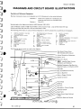
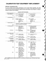
SERVICE INFORMATION
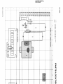
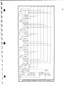
Symbols and Reference Designators
Rear Interface Connectors (reverse side)
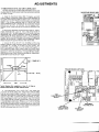
Test Equipment Required/Controls & Connectors
Adjustments (reverse foldout)
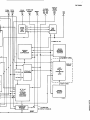
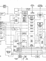
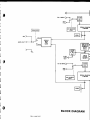
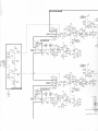
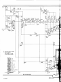
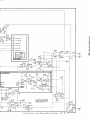
Block Diagram
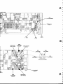
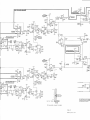
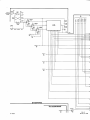
Parts Location Grid Trigger Circuit Board (backside of
foldout)
Input, Trigger, 10° DCU & Power Supply
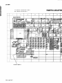
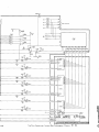
Parts Location Grid Main Circuit Board (backside of
foldout)
Gate and Control Logic, Averaging Divider, and Reset
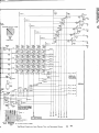
Parts Location Grid Main Board (Back) and Display Circuit
Board (backside of foldout)
1
MOS Interface, 10 -106 DCU and Latches, and Overflow
Time Slot Generator, Leading Zero Suppression and
Display
Time Base, Phase Lock Loop, and Decimal Point &
Parameter Matrix
SECTION 6
4-1
5-1
0
0
0
¢
~
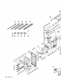
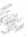
MECHANICAL PARTS LIST
Fig. 1. Exploded
CHANGE INFORMATION
iii
[
DC 505A
UNIVERSAL COUNTER I TIMER
I•
r
-
-
DC 505A
--
-
Section 1-0C SOSA
OPERATING
INSTRUCTIONS
•
INTRODUCTION
The DC 505A Universal Counter/Timer has seven
measurement functions: frequency counting, finding frequency ratios, period timing, interval timing, width timing,
electronic event counting, and manual event counting.
The DC 505A has two input channels (A & B), each
having bnc inputs and separate triggering level,
attenuators, and coupling mode controls. Both input
channels have the same 225 MHz capability. Sevensegment light-emitting diode arrays (LED's) provide a
seven-digit visual numerical display. The decimal point is
automatically positioned and the leading zeros (to the left
of the most significant digit or decimal point) are blanked.
Digit overflow is indicated by a flashing display.
•
Signals to be counted/timed can be applied to either or
both channel A or channel B front-panel bnc connector or
to the rear interface connector. The DC 505A is designed
to operate in a TM 500-Series Power Module.
The DC 505A can be ordered equipped with a
temperature-compensated, 5 MHz crystal oscillator to
obtain a highly stable and precise internal time base. This
option includes a divide-by-five IC counter to produce the
1 MHz clock.
The triggering level of CH A or CH B can be adjusted to
a fixed voltage level by monitoring a dc voltage at a frontpanel LEVEL OUT jack, or at the rear interface.
Installation
The DC 505A is calibrated and ready for use as
received. Turn the Power Module OFF before inserting the
instrument. Do not use excessive force when installing the
DC 505A and be certain that the front panel of the
instrument is aligned with the edges of the Power Module
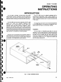
compartment. Refer to Fig. 1-1; install the DC 505A and
turn the Power Module ON.
POWER
MODULE
Top
Groove
Bottom
Groove
•
Fig. 1-1. Plug-In Installation/removal.
REV. A APR 1977
1-1
Operating Instructions-DC SOSA
When DC 505A's with serial numbers B010630 and
above are to be installed in the low-power compartments
of a particular TM 500 Power Module, modifications to the
Power Module must be performed as indicated below.
Refer these Power Module modifications to qualified
service personnel.
2. TM 504 with more than two DC 505A's installed:
Change F35 (5 A fuse) to a 7.5 A fuse, Tektronix Part
Number 159-0096-00.
3. TM 515 with more than three DC 505A's installed:
Change F135 (7.5 A fuse) to a 10 A fuse, Tektronix Part
Number 159-0057-00.
1. TM 503 with more than two DC 505A's installed:
4. TM 506 with more than three DC 505A's installed:
Replace C35 (11,000 tJF) with a 18,000 tJF capacitor,
Tektronix Part Number 290-0508-01.
Change F35 (7.5 A fuse) to a 10 A fuse, Tektronix Part
Number 159-0057-00.
OPERATIONAL CHECK
TABLE 1-1
Controls and Connectors
Pull out the tab labeled "Controls, Connectors, and
Rear Connector Pin Assignments" (at the rear of the
manual) to expose the front panel illustration. Review the
functions of the controls, connectors, and indicators
before continuing with the operational checks.
GATE TIME
.01
.1
1
10
s
s
s
s
Unit Indicators
Decimal Point
MHz
MHz
kHz
kHz
.0000
.00000
.000
.0000
•
Display Tests
With no signal applied, test the DC 505A's reaclout
displays and switching logic. The following checks will
test most of the counter's major circuits and ensure its
readiness to make measurements. If any malfunctions are
detected, first refer to the Adjustment Procedure in the
service section of this manual, then the System
Maintenance Section of the Power Module manual.
With the DISPLAYTIMEcontrol in thefull ccw position,
observe that the GATE indicator flashes rapidly for short
GATE TIMEs and more slowly for longer GATE TIMEs.
Using a short GATE TIME, rotate the DISPLAY TIME
control slowly cwo Observe that the GATE light will stay off
for a longer and longer time, until the control clicks into
the HOLD detent position, holding off the GATE indefinitIy. Return the DISPLAY TIME control to the ccw position.
Readout Segment Test. Press the RESET button to
check the seven character segments of each digit. A row of
8's should be displayed. This check of the display devices
and drivers can be done at any time.
FREQ A Displays. Using the FUNCTION switch, select
a FREQ A GATE TIME of .01 s. Check the decimal point
location, leading zero suppression, and units indicators
according to Table 1-1. The decimal point and units
indicator lights in any setting should not change when
either the N switch or CLOCK RATE switch positions are
changed.
1-2
RATIO AlB and EVENTS A DURING B Displays. Set
the FUNCTION switch to RATIO AlB and the N switch to
105 • Check the readout displays according to Table 1-2.
Set the FUNCTION switch to EVENTS A QURING Band
the N switch to 105 . Again check the readout displays
using Table 1-2. (Changing the CLOCK RATE switch
should have no effect on the decimal pOint appearing In •
the readout display in either of these FUNCTION switch
settings.)
)
REV. A APR 1977
o
Operating Instructions-DC 505A
:Jet
:J
:J
:J
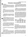
TABLE 1-2
N Switch
Decimal Point
5
10
4
10
3
10
2
10
10
1
.00000
.0000
.000
.00
.0
a
The GATE and units indicators should remain off.
PERIOD B, TIME A-B and WIDTH B Displays. Set the
FUNCTION switch to PERIOD B, the CLOCK RATE
5
switch to 10 ns and the N switch to 10 . Check the readout
display according to Table 1-3.
:1
:1
~.
:1
Change the FUNCTION switch to TIME A-B. Retain
the same settings on the CLOCK RATE and N switches.
Check the readout displays according to Table 1-3.
Change the FUNCTION switch to WIDTH B and make
the same check of the readout displays using Table 1-3.
NOTE
Table 1-3 and the diagram are drawn as an aid to
troubleshooting if the decimal pOints and units
indicators are non-functioning or incorrect in any of
the time interval measurement settings. See Theory
of Operation, Decimal Point and Parameter Selection.
:1
i
5
~
5-
?
Table 1-3
CHANNEL A SLOPE. With the FUNCTION control set
to TOTALIZE A, CH A to +SLOPE, depress IN: START,
OUT: STOP button. Turn the CH A LEVEL control knob
fully CWo Readout display should increase one count each
time the knob is turned from cw to ccw (past centered
LEVEL position). Verify that the count does not increase
when the knob is turned from ccw to cwo
Change to -SLOPE. Push the RESET button to clear
the display. Readout should now increase one count each
time the CH A LEVEL control is turned from ccw to cwo
Turning the LEVEL control from cw to ccw should not
increment the display.
CHANNEL B SLOPE. Set FUNCTION control switch to
PERIOD B, CH B to +SLOPE, N (averaging factor) control
to 1. Push the RESET button. Check that the GATE light
turns on when the CH B LEVEL control knob is turned
from the cw to the ccw position. Turning the knob back to
cw should have no effect on the GATE light. Another turn
from cw to ccw turns the light off.
Change to -SLOPE. Push the RESET button. Check
that the GATE light turns on when CH B LEVEL control
knob is turned from ccw to cwo The light should remain on
when the knob is turned back to ccw. The GATE light turns
off on the next turn from ccw to cw of the LEVEL control
knob.
Front-panel
Controls
Readout Display
UNITS
INDICATOR
TOTALIZE A Display. Set the FUNCTION switch to
TOTALIZE A. Observe a zero at the right of the readout
display. The GATE light should turn on when the IN:
START, OUT: STOP button is pushed in, and turns off
when button is released. The units indicators and decimal
points should remain off.
Channels A & B. The channel A & B input circuits, with
the exception of the attenuators, can be checked in a nosignal-input condition by generating pseudo-triggers with
the LEVEL controls.
DECIMAL
POINT
mS
0
mS
.0
mS
.00
mS
.000
I1S
.0
CLOCK RATE
SWITCH
I1S
.00
1 mS
I1S
.000
.1 mS
nS
.0
10 J1S
nS
Select +SLOPE for one channel and -SLOPE for the
other channel. Set FUNCTION to TIME A-B, CLOCK
RATE switch to 1 ms and N switch to 1. Rotate CH A
LEVEL back and forth through its selected slope until the
GATE light turns on. Rotate CH B LEVEL back and forth
through its selected slope until the GATE light turns off.
The resultant display is the time interval between these
two trigger events.
nS
nS
10' 10' 10' 10'
N Switch
REV. A APR 1977
If the GATE light cannot be turned on or off with this
method, consult the Service section of the manual for
troubleshooting aids.
1-3
Operating Instructions-DC SOSA
RATIO AlB Check. Connect an approximately 1 to
5 MHz signal from a signal source, for example the
SG 503, into the input of both CH A and CH B using a Dual
Input Coupler (Tektronix Part No. 067-0525-00). Set the
FUNCTION control switch to RATIO AlB, +SLOPE on
both channels. Check the readout display according to
Table 1-4.
TABLE 1-4
Change both channels to -SLOPE and make the same
check of the readout display using Table 1-4.
N Switch
Decimal Point
(±1 count)
105
10 4
103
10 2
10
1
1.00000
1.0000
1.000
1.00
1.0
1
•
INPUT CONSIDERATIONS
Input Sources
Sensitivity and Frequency Range
The switch concentric with the LEVEL control of each
channel selects either the front-panel bnc connector
(external), or the rear interface connector (internal) pins;
Channel A via pin 16A, and Channel B via pin 17B.
CH A and CH B will respond to signal amplitude of at
least 50 mV rms sinewave, times attenuation, to 150 MHz,
and 100 mV rms sinewave, times attenuation, from
150 MHz to 225 MHz.
The External inputs present high impedance of approximately 1 MO, paralleled by about 24 pF. The Internal
input circuits present nominal 50 0 impedances to match
typical coaxial cable signal connections.
Depending on the coupling mode selected, the low
frequency limit for each channel is either 0 Hz (dccoupled) or 10 Hz (ac-coupled).
•
Input Coupling
Front Panel push buttons select ac (Capactive) or dc
(Direct) coupling for each channel's input signal. This
coupling takes place after the signal arrive from the
selected source and before they are passed on to the
attenuators of each channel.
Attenuators and Maximum Input Volts
The front-panel pushbutton, when out, provides no
attenuation to the input signal (X1). In this mode, the
maximum safe input voltage is 50 V (dc + peak ac), at
10 kHz or less (CH A or CH B). With the X20 attenuator
selected, the maximum safe input voltage is 250 V (dc +
peakac) at 1 MHz or less (CH AorCH B). (See Table 1-6.)
Slope and LEVEL
A front-panel pushbutton for each channel determines
whether the trigger circuits will respond to either positive- .
or negative-going transitions of each input signal.
The LEVEL control for each channel allows the
operator to move the hysteresis window of the trigger
circuit to an optimum level on the input signal to ensure
stable triggering. See Fig. 1-2. The LEVEL control adjusts
over ±2.0 V of the input signal in the X1 attenuation
position. This level can be monitored at the front-panel
LEVEL OUT pin jack.
40-millivolt
typical
a:
a:
c
c
_/'W;\~
c
(A) Erroneous count.
(8) Correct count.
L---------------F-I-9-.1---2-.-T-rl-g-g-er-ln-g--CI-rc-u-lt-r-e-sp-o-n-s-e-s-to--Im-p-r-o-pe-r-(-A-)-a-n-d-p-ro-p-e-r-(-B-)-L-E-V-E-L-s-et-ti-n-gs-.---------------J
1-4
REV. A APR 1977
.c
~
]
Operating Instructions-DC 505A
FREQUENCY MEASUREMENTS
FREQUENCY A
To measure and display the frequency of a signal up to
22S MHz, set the FUNCTION switch to one of the shorter
GATE TIMEs bracketed under the heading of FREQUENCY A. Make sure the LEVEL control is pushed in and
connect the signal to the CH A INPUT. Set the DISPLAY
TIME control ccw.
J
Triggering
The CH A LEVEL, Slope, Coupling, and attenuator
controls all affect the ability to make a measurement. In
general, the trigger controls are similar to oscilloscope
controls, except that the end result is not a stable
waveform graphic display, but a stable digital frequency
display.
Coupling and Slope. Use ac-coupling for most frequency measurements to avoid re-adjusting the LEVEL control
for changing dc levels. The repetitive nature of the signals
makes Slope selection insignificant for frequency
measu rements.
•
J
Attenuators and LEVEL. Signals less than 3 V peak-topeak, should not be attenuated. For higher amplitude
signals, select an attenuation factor such that the
attenuated signal falls into the range of 1S0 mV to 4 V,
peak-to-peak. The LEVEL control must be varied for a
stable reading. It will not be touchy unless the signal
amplitude and frequency are close to (or perhaps beyond)
the specified limits.
A signal that looks stable on an oscilloscope may still
show jitter when measured with 7-digit resolution. If the
count varies from reading to reading, it is probably due to
jitter in the signal source. If the count changes unreasonably, the DC SOSA is not being triggered properly,
either because the controls are not set right or the signal is
beyond the counter's capabilities.
For frequency measurements, all CH B trigger settings
have no effect. "N" or "CLOCK RATE" settings are
irrelevant.
Measurement Intervals
To adjust the trigger controls, choose a short GATE
TIME such as .1 s or .01 s. This gives rapid feedback via
the display as to whether the counter is being triggered or
not. If it is, numbers will appear in the display. (If the
frequency is below 100 Hz, numbers may not appear
during the shortest gate times. For such low frequencies, a
PE.RIOD measurement is better suited.)
@
Final selection of GATE TIME depends on the frequency being measured, desired resolution, and willingness of
the operator to wait for a measurement. Using short gate
times, higher frequencies may be measured, but at the
expense of the greater resolution capabilities ofthe longer
gate times.
Resolution. A 10 s GATE TIME means the operator
must wait 10 seconds for a measurement to be made and
displayed. It is the only way to get best possible resolution
and accuracy for signals below 1 MHz. Even then, a 10
second count will display fewer than the available 7 digits.
Overflow. Through intentional use of "overflow" displays, it is possible to improve the resolution of the
counter. Choose a GATE TIME that displays the most
significant number of the measurement as far to the left as
possible. Note the numbers displayed to the right of the
decimal. Move the decimal point to the left by choosing
longer GATE TIMEs until the desired resolution is achieved. The display will flash when the most significant
number overflows the last storage register. The
relationship between GATE TIME, measured frequency,
displayed digits, and overflow is shown in Table 1-S.
TABLE 1-5
GATE
TIME
.01
.1
1
10
s
s
s
s
>100 MHz
7 digits
Overflow
Overflow
Overflow
10 MHz to 1 MHz to
100 MHz
10 MHz
6 digits
7 digits
Overflow
Overflow
S digits
6 digits
7 digits
Overflow
<1 MHz
4
5
6
7
digits
digits
digits
digits
Measurement Rate
Once a stable measurement is obtained, the rate at
which measurements are made can be controlled by the
DISPLAY TIME control. Turning the control cw holds off
the gate and stores the display for a longer time before a
new measurement is made and displayed. DISPLAYTIME
and GATE TIME together complete a measurementdisplay cycle.
The DISPLAY TIME control is uncalibrated and
variable from about 0.1 s at the ccw end to about 10 s at
the cw end. At the cw end, there is a detent position called
HOLD. In HOLD, the last count taken will be stored and
displayed for an indefinite time. A new count and display
may be initiated by pushing the RESET button, turning the
DISPLAY TIME control ccw, or changing to another GATE
TIME.
1-5
Operating Instructions-DC 505A
RATIO MEASUREMENTS
In the RATIO AlB mode, the frequency of the signal
applied to CH A is divided by the frequency of the signal
applied to CH B, and the resultant ratio is displayed. Note
that the normal "frequency" mode is basically a ratio
mode, in which the ratio of the unknown signal to the
internal clock is displayed. (Decade scaling of the internal
clock and decimal point positioning normalizes the display relative to kHz or MHz units.)
2. Go to the PERIOD B mode and adjust the CH B
trigger controls for a normal period measurement.
.---0
3. Leaving CH A and CH B trigger controls as they
were, go the RATIO A/B mode. The correct ratio should be
displayed.
Triggering
The operation of CH A and CH B trigger controls is the
same as for frequency and period measurement. In fact,
since both channels must be triggered to obtain a display,
it may be desirable to set the trigger controls independently. This may be accomplished as follows:
1. Go to the FREQUENCY A mode and adjust the CH A
trigger controls for a normal frequency measurement.
Resolution
The N switch may now be operated to select maximum
resolution. For most measurements, the smallest value of
"N" that produces a useful number of digits will be best.
PERIOD MEASUREMENTS
Gating
Averaging
Period measurement is provided in universal
counter/timers primarly to overcome a basic limitation of
counters, i.e., the long time required to make a high
resolution, high accuracy measurement of low frequency
signals. For example, a 1 kHz signal requries 1,000
seconds of GATE TIME to accumulate a million counts.
However, in only one second, a 1 kHz signal can gate a
count of one million clock pulses from a 1 MHz clock.
Resolution and accuracy is improved by averaging the
signal value over a large number of signal events. This
increases the total time to take a measurement, i.e., similar
to selecting a longer GATE TIME in the FREQUENCY A
mode. The best resolution possible for period
measurements is 0.1 ps.
Simply stated, the PERIOD B mode reverses the
functions of signal and clock as compared to the FREQUENCY A mode. In FREQUENCY A, the gate is held
open for some number of clock pulses while signal events
are counted, then displayed. In PERIOD B, the gate is held
open for some number of signal events (N), while clock
pulses are counted, then displayed.
Low Frequencies
Period measurements of signal below 10 Hz, and
particularly in the lowest decade from 0.1 Hz to 1.0 Hz,
become rather sensitive to wave shape and amplitude.
Since it is desirable for the signal to pass through the
trigger hysteresis abruptly, square waves are preferred.
Wave shapes other than square-waves can be measured
accurately at the very low end and if the input amplitude is
kept high so that the trigger input is driven hard.
TIME INTERVAL MEASUREMENTS
General
Time interval measurements are performed using the
TIME A~B or WIDTH B modes. The TIME A~B mode
measures and displays the elapsed time interval between
the triggering level of CH A and the subsequent triggering
level of CH B. The WIDTH B mode measures and displays
the elapsed time interval between the selected triggering
level on the starting slope of the pulse duration to be
measured and the same triggering level on the opposite
polarity ending slope.
1-6
The voltage levels necessary to establish the triggering
points on any selected slope are monitored and set with
DVM readings at the CH A/CH B LEVEL OUT pin jacks on
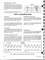
the front panel or on pin 22A at the rear interface. Fig. 1-3
illustrates typical LEVEL OUT voltage settings for various
time interval measurements. Fig. 1-3 is limited to positivegoing pulses above ground reference (0 V), but the same
procedure is essentially followed for input signals whose
peak-to-peak amplitude falls within the triggering level
range. Only the voltage polarities and +SLOPE or
@
[
-
.
[~
Operating Instructions-DC 505A
•
-SLOPE selection need be considered when determining
triggering levels not illustrated in Fig. 1-3. When making
these measurements, each channel must be DC COUPLED and coaxial cables must be terminated properly in
order to maintain signal fidelity.
WIDTH B Mode
In order to measure pulse duration (Fig. 1-3, waveform
3) the 50% level must be determined. Apply the input
signal to CH B (use X1 ATTEN) and set FUNCTION switch
to WIDTH B. Set CH B LEVEL control fully counterclockwise (clockwise for input signals below ground).
GATE light must be out.
Rotate CH B LEVEL control until the GATE light just
comes on and record the first DVM reading. Continue
rotating CH B LEVEL control until the GATE light just goes
out and record the second DVM reading. If the GATE light
does not go out, reduce input signal amplitude or use X20
ATTEN. Subtract first DVM reading from second reading
to obtain the peak-to-peak amplitude, then divide by 2.
The answer is the desired 50% level. Reset CH B LEVEL
control so that DVM indicates the 50% level, then read the
pulse duration from the DC 505A display.
NOTE
TIME A-B Mode
Rotating a level control moves the triggering
hysteresis window up or down through the peak-topeak amplitude swing of an input signal. Any time
that the GA TE light is out, the hysteresis window is
outside the signal limits and the counter is not
triggered. The hysteresis window is typically about
40 mV.
•
This measurement requires input signals to both CH A
and CH B, but peak-to-peak signal amplitudes should first
be determined using the WIDTH B mode (refer to WIDTH
B Mode instructions). For TIME A-B measurements,
follow these steps:
1. Set FUNCTION switch to WIDTH B.
, . . - - - -....... - - - - -
A LEVEL
SET
:;"2.00 V
,
,,,
0.00 V
I
.
,I
.
, TIME!
: A-BI
,MODE
B LEVEL
SET
, - - - - -..... - - 2.00 V
,
--- ---,,
, 1.00 V
B LEVEL
SET
A LEVEL
SET
---/T 10%
,,,
,
1.00 V,
: DURATION
I
:---WIDTH B - '
MODE
I
,
,
,,,
----.--,
o
90%
RISETIME
+ SLOPE
o
90% ,
FALLTIME
- SLOPE
®
OaOO V
______ A LEVEL
SET
,
,,
:10% '--,
I
, :
I
OV
~L~~iL
50%)
B LEVEL
SET
,
TIME
A-B
MODE
Fig. 1-3. Typical CH A and CH B LEVEL OUT voltage settings for various time interval measurements.
@
1-7
r:
Operating Instructions-DC 505A
2. Using a DVM, the CH B LEVEL control, and the
GATE light indications, determine the peak-to-peak
amplitude of the signal to be applied to CH B. Calculate
desired triggering level for CH B.
3. If signal to be applied to CH A is different in
amplitude than CH B signal, repeat step 2 to determine the
peak-to-peak amplitude of the signal to be applied to CH
A. Calculate the desired triggering level for CH A.
4. Set CH B to desired triggering level as calculated in
step 2.
5. Set FUNCTION switch to TIME A-B.
of time interval measurements on repetitive signals. The
basis of time interval averaging is the statistical reduction
of the ±1 count error. If the ±1 count error istrulyrandom,
then as more intervals are averaged, the measurement will
tend to approach the true value of the time interval. For
time interval averaging to work, the time interval being
measured must be repetitive and have a repetition frequency that is non-synchronous to the counter clock rate.
.c
c
Time interval averaging of N>1 should be used
whenever the ±1 count error of a repetitive signal
(averaging switch actually set to 1) significantly degrades
the accuracy and resolution of the measurement. When 8
measurement is made and the least significant digits
appear unstable (due to inherent instrument noise),
improvements in accuracy and resolution can be obtained
by either increasing the average factor N, or increasing the
CLOCK RATE.
.
6. Set CH A to desired triggering level as calculated in
step 3.
Single-Shot using HOLD
7. With signals connected to the proper channels, read
the elapsed time interval between the triggering level of
CH A and the subsequent triggering level of CH B.
Time Interval Averaging
Time interval averaging provides an economical
method of greatly increasing the accuracy and resolution
Single-shot time intervals can be measured in either the
TIME A-B or WIDTH B modes by setting the DISPLAY
TIME control to the HOLD position. For the HOLD
position, the counter makes a single measurement (wl~
the function averaged over N cycles of B or A-B), displays "
the count and holds the answer until the operater pushes
the RESET button to clear the display and rearm the
counter circuits for another single-shot measurement. '
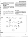
EVENT MEASUREMENTS
In the EVENTS A DURING B mode, signal events
applied to CH A INPUT are counted and the accumulated
total is displayed for the time that the signal applied to CH
B INPUT causes channel B to be triggered high and the
counter/timer gate opened. This mode is similar to the
TOTALIZE A mode.
The following procedure can be used to make a
measurement like that shown in Fig. 1-4.
slope switch to +SLOPE. Adjust the CH B LEVEL for a
stable period display.
3. Set the FUNCTION switch to EVENTS A DURING B.
4. When the CH B signal excursion occurs, CH B is
triggered and the gate opens, allowing the CH A pulses to
be counted.
Averaging
1. Apply the events to be counted to CH A. Set the
FUNCTION switch to FREQUENCY A and CH A slope
switch to +SLOPE. Adjust the CH A LEVEL for a stable
frequency display.
2. Apply the counter/timer gate open control signal to
CH B. Set the FUNCTION switch to PERIOD Band CH B
1-8
Averaging provides an economical method of increasing the accuracy and resolution of repetitive event
per interval measurements. The basic of averaging is the
statistical reduction of the ±1 count error. If the ±1 count
error is tru Iy random, then as more intervals are averaged,
the measurement will tend to approach the true value of
the number of events per interval. For averaging to work,
the events being measured must be repetitive.
@
c
C
C
C
C
C
\
s-
5.
5
5"
~j
Operating Instructions-DC 505A
Counter/Timer
Gate Open Time
I
I
1
I
I
i(
·1
CH B Input
Signal
CH A Input
Signal
Fig. 1-4. illustration depicting CH A pulses and portion of CH A pulses being counted during the counter/timer gate open time
(controlled by CH B signal).
Event per interval averaging should be used whenever
the ±1 count error from a single event per interval
measurement (N switch actually set to 1) significantly
degrades the accuracy or resolution of the measurement.
When using averaging, the inherent·instrument noise will
limit the resolution of the measurement.
The accuracy of the event per interval averaging
measurement can be determined by using the following
~
ormula:
fractional part only of 1 1-
freq into CH A
freq into CH B
I) IN >
fractional resolution required
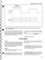
TOTALIZING
Purpose
In the TOTALIZE A mode, signal events applied to CH A
INPUT are counted and the accumulated total is displayed
during the time the IN: START, OUT: STOP button is
pushed in. This mode is a manual analog of the frequency
mode. Its main application is to accumulate a count of
relatively slow and irregular events.
Operation
whole numbers. Only the CH A trigger controls. The
RESET button, and the IN: START, OUT: STOP button
affect the display.
Stopping the Count. If the IN: START, OUT: STOP
button is released and no other controls are operated, the
last total will continue to be displayed. No more incoming
events will be added to the total.
Apply the signal to CH A and set the trigger controls the
same as for frequency measurement.
Starting the Count. Press the IN: START, OUT: STOP
button in and adjust the CH A LEVEL control until a count
begins to advance. The accumulated count is displayed in
@
Restarting and Resetting. When the IN: START, OUT:
STOP is again depressed, incoming events will advance
the displayed total. Resetting the count to zero can be
done at any time by pressing the RESET button.
1-9
Operating Instructions-DC 505A
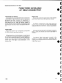
FUNCTIONS AVAILABLE
AT REAR CONNECTOR
e
Customizing the Interface
Signal Lines
Unassigned pins are available at the rear connector for
routing signals to and from the DC 505A for specialized
applications (see Rear Connector Pin Assignments in
Section 5). One or more compartments of a multi-plug-in
Power Module can be wired with barriers installed to
provide specific functions between compartments. See
Power Module instruction manual for additional information.
These lines provide for signal input to each channel
status, clock signal outputs and BCD data outputs.
The Reset, Time-Slot Zero (TSO), Data Good, and
Overflow lines report the status of the DC 505A. BCD data
lines report the count in an 8-4-2-1, serial-by-digit method.
Control Lines
These lines allow the user to externally command the
DC 505A to certain operating conditions.
A Reset input line, which doubles as an output signal
line, clears the counter to zero when a low is applied to it.
An input line to disable the flashing overflow display also
doubles as an output signal line during overflow. The IN:
START, OUT: STOP signal is also addressable via the
interface lines.
1·10
As long as the Internal Scan Clock Disable line remains
high (or open), the Internal Scan Clock output signal is
available.
The internal 1 MHz Clock signal is brought to the
interface for possible synchronous applications. (An
internal switch allows this same line to be used for external
1 MHz Clock input.)
@
e
t:
C
t:
L
L
e·
C
L
L
Operating Instructions-DC 505A
•
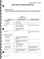
ELECTRICAL CHARACTERISTICS
Performance Conditions
The electrical characteristics are valid only if the DC 505A has been calibrated at an ambient temperature between
+20°C and +30°C and is operating at an ambient temperature between O°C and +50°C, unless otherwise noted.
TABLE 1-6
Channels A and B Input
Characteristics
Performance Requirements
Supplemental Information
Frequency Range
DC Coupled
o Hz to 225 MHz
AC Coupled
10 Hz to 225 MHz
Sensitivity
50 mV rms sine-wave times
attenuation to 150 MHz
Sine-wave used for measurement
100 mV rms sine-wave times
attenuation from 150 MHz
to 225 MHz
Impedance
1 MO paralleled by approximately
24 pF
Maximum Input Voltage
(sine waves, dc + peak ac)
•
X1 Attenuation
CH A or CH B
50 V at 10 kHz or less; derate -20 dB/
decade to 100 kHz. 5 V at 100 kHz
to 225 MHz.
X20 Attenuation
CH A or CH B
250 V at 1 MHz or less; derate -20 dB/
decade to 50 MHz. 5 V at 50 MHz
to 225 MHz.
Trigger Level Range
-2 V times attenuation to
+2 V times attenuation
Trigger Level Output
(CH A or CH B)
At least -2 V to +2 V
Monitored at front-panel jack or
pin 22A at rear interface
Signal Source
Internal (rear connector interface)
or external (front-panel bnc)
Selected by pushing in or pulling out
front-panel LEVEL control
Slope
Either + or-
REV. B, AUG. 1977
1-11
[I
Operating Instructions-DC 505A
J
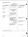
TABLE 1-7
[
Display Resolution and Accuracy
------~------~-------
Characteristics
Performance Requirements
Supplemental Information
e1
[
FREQ A
Accuracy
±1 count ± time base accuracy
Signal to noise ratio at inputs
must be ;':40 dB
RATIO AlB
Accuracy
±1 count of FREQ A ± trigger jitter
error of channel B (see Note 1)
+
Frequency into A
0.3 X 10 8
PERIOD B
Accuracy
±1 count ± time base accuracy
± trigger jitter error of count B
(see Note 1) +2 counts (applies to
10 ns clock rate only)
Resolution
0.1 ps
TIME A-B
Accuracy
±1 count ± time base accuracy
± trigger jitter error of channel
A
(see Note 2) ± chosen time
base periodl VN
± channel delay match error of 2 ns
+ (10 ns)
input step volts to
Volt
LEVEL setting of B
(B
_
A input step volts to)
LEVEL setting of A
+2 counts (applies to 10 ns clock
rate only) + Note 4 condition
satisfied (see Fig. 1-5)
Resolution (Practical Limit)
TIME A-B best absolute accuracy
with averaging is 3 ns
Pulse widths minil'l1um into channel
A and B (for TIME A-B)
is 5 ns
N is the averaging factor
100 ps
•
1-12
REV. B, AUG. 1977
Operating Instructions-DC SOSA
TABLE 1-7 (cont)
Supplemental Information
Performance Requirements
Characteristics
± time
WIDTH B
WIDTH B best absolute accuracy
with averaging is 1.5 ns
base accuracy +
(Hysteresis error and trigger jitter
error, see Note 3) ± chosen
time base period)/N
+
(10Voltsns) (LEVEL
setting of
B to pulse height
Refer to
Fig. 1-5
_ Baseline to LEVEL)
setting of B
+2 counts (applies to
rate only)
10 ns clock
+ Note 4 condition satisfied
Resolution (Practical Limit)
100 ps
EVENTS A DURING B
Accuracy
•
± period of signal AlN
+ (Hysteresis error and trigger
jitter error of CH B)
(see Note 3)
(10Voltsns)
+ (Frequency Of)
\events into A
LEVEL setting of B
( to pulse height
Baseline to LEVEL)
setting of B
Refer to
Fig. 1-5
+ Note 4 condition satisfied
NOTES
1. Trigger jitter error =
(Ratio, Period)
2. Trigger jitter error =
(Time A~B)
(dVidl of I~?~g~ring edge)/N
l
0.005 V
\dV/dt of start edges
±
0.005 V
) /
dV/dt of stop edges
VN
3. Hysteresis error and Trigger jitter error=
0.1 V
dV/dt of stop edge
+(
-
0.005 V
dV/dt of start edges
±
0.005 V
)/
dV/dt of stop edges
'IN
N is averaging factor
dV/dtislimitedtoamaximumofO.2 V/2 nsby
the amplifier risetimes
REV. A, AUG. 1977
1-13
Operating Instructions-DC 505A
TABLE 1-7 (cont)
4. (A) For TIME A-8 and WIDTH 8 measurements, the
internal clock rate and the repetition rate of the
measured interval must not be synchronous.
(8) For EVENTS A DURING 8, the repetition rates of
the signals applied to A and 8 must not be
synchronous.
liI..ni
Volt
Level
Pulse
Height
Setting
L-.,----:,,.:-__--.,
Input
Volts
/
/
\
\
---===::;::-r--r,/l- - - - -- - \
dt
Baseline
--
start
dt
-
stop
Fig. 1-5.
TABLE 1-8
Internal Time Base
Characteristics
Performance Requirements
Standard
Option 1
Crystal Frequency
1 MHz
5 MHz
Stability (O°C to +50°C)
After 1/2 Hour Warm-up
1 part or less
in 105
Within 5 parts
7
in 10
Long-Term Drift
1 part or less in
105 per month
1 part or less in
107 per month
1 MHz Clock Signal
Adjustable to
within 1 part
in 107
Adjustable to
within 5 parts
in 109
1-14
Supplemental Information
•
REV. A APR 1977
]
Operating Instructions-DC 505A
TABLE 1-9
Display
Characteristics
Performance Requirements
Display Time
Variable from about 0.1 s to about
10 s. Detent position at cw
position of DISPLAY TIME knob
provides a HOLD mode.
Reset
Pushing the front-panel RESET
pushbutton, or grounding pin 26A
of the interface connector, resets
the counter to zero and totally
lights the display (except for
the decimal points) for a lamp test.
]
]
Supplemental Information
]
]
]
TABLE 1-10
Outputs
]
Characteristics
A OUT
Logic Levels
0
1
Propagation Delay
from Channel A INPUT
to A OUT
]
Approximately -0.1 V into open
circuit
Approximately +0.1 V into open
circuit
Approximately 15 ns
B or A-B OUT
]
Logic Levels
0
1
Approximately -0.1 V into open
circuit
Approximately +0.1 V into open
circuit
]
Propagation Delay
from Channel Inputs
to B or A-B OUT
]
]
]
Supplemental Information
Performance Requirements
Approximately 15 ns
Shaped output, after trigger level
and slope selection, of the signal
into channel A INPUT connector.
Output represents the display information for FREQUENCY A, RATIO
AlB, and TOTALIZE A modes
50
n
reverse terminated.
Shaped output after trigger level
and slope selection of either the
Channel B signal or the A-B
signal. This output represents the
continuous signal used in generating
the display gating for the RATIO
AlB, PERIOD B, TIME A-B, WIDTH
B and EVENTS A DURING B modes.
50
n
reverse terminated.
•
@
1-15
[
Operating Instructions-DC SOSA
TABLE 1-11
•
Environmental
Characteristics
Performance Requirements
Supplemental Information
Temperature
Operating
Storage
O°C to +50°C
-40°C to +75°C
Forced air circulation is required from +40°C to +50°C
Altitude
Operating
Storage
To 15,000 feet
To 50,000 feet
Vibration
Operating and NonOperating
With the instrument complete and
operating, vibration frequency swept
from 10 to 50 to 10 Hz at 1 minute
per sweep. Vibrate 15 minutes in each
of the three major axes at 0.015"
total displacement. Hold 3 minutes
at any major resonance, or if none,
at 50 Hz. Total time, 54 minutes.
Shock
Operating and NonOperating
1-16
30 g's, 1/2 sine, 11 ms duration,
2 shocks in each direction along
3 major axes, for a total of
12 shocks
@
[J
Section 2-0C 505A
THEORY OF
OPERATION
INPUT AND TRIGGER
AC/OC Selection, Attenuators, And Coupling, CH A
& (B)
Channels A and (B) are identical with regard to the
amplifiers. The input signal, applied through front-panel
INPUT connector J210 (J100), first passes through frontpanel push-button switch S215A (S105A) to select ac or
dc. X1 or X20 attenuation is selected by front-panel pushbutton switch S215B (S105B). X20 ATTEN is a frequencycompensated voltage divider, composed of resistor R220
(R110) and Capacitor C222 (C112).
The input signal is coupled to the input field effect
transistor, FET 0235A (0125A) which acts as a source
follower. The RC protection circuitry, consisting of
capacitor C232 (C122) in parallel with resistor R232
(R122), transmits the Signal to reverse-biased diode
CR232 (CR122) at the gate of the input FET's.
Input Amplifier, Signal Shaping, Slope Selection
And Output
The source follower, 0235A (0125A), couples the
Signal to the base of an emitterfollower, 0240 (0130), that
drives a complimentary cascode amplifier, 0242 and 0270
(0132 and 0160).
Adjustment of the LEVEL control at the base of 0270
(0160) changes the bias on that transistor selecting which
portion of the input Signal will trigger the DC 505A.
Resistors R264 and R265 (R154 and R155) ganged around
the LEVEL control, R260 (R150), in conjunction with
resistors R262 and R258 (R152 and R148) from either end
represent a reverse S-Curve. This allows good sensitivity
at the center with a wide dynam ic range, in excess of 20 to
1, necessary for the X20 attenuation. The diode, CR264
(CR154), between the center arm of the LEVEL control and
the resistor, R268 (R158), at the base of 0270 (0160)
provides first-order temperature compensation.
The collector of 0270 (0160) is the output of the trigger
amplifier which has a gain of approximately 5. This is
coupled through emitter follower 0275 (0165) to a
Schmitt Trigger, 0280 and 0282 (0170 and 0172). The
output of this signal shaper, the collector of 0282 (0172),
@
is ECL compatible and drives the slope selection gate,
U190B (U190C). The SLOPE switch, S295 (S185), selects
the triggering slope by allowing either a high or a low to
drive the exclusive OR slope selection gate.
The shaped Signal from both channels is transmitted to
the TIME A-B circuitry and the signal selection circuitry.
The signal from Channel A couples into U200D to provide
shaped output at pin 15 of U200D, which drives resistor
R305, R308 to ground and resistor R307 to -10 V, for
output to the front panel, A OUT (J310). The signal from
Channel B is coupled through additional gates in the
Signal Selection circuitry to exclusive OR gate. U190A, to
provide shaped output at pin 2 of U190A. This drives
resistor R202, R204 to ground and R205 to -10 V, for
output to the front panel, B or A-B OUT (J205). Both
OUTPUTS are centered around approximately 0 volts
with =0.25 volt drive from 50 O.
Signal Selection
The output from pin 2 of U195A or pin 3 of U200B, a
hard wire or ECL combination, is either the shaped signal
from Channel A or the Time Select from the front panel.
The Time Select ranges from 10 ns to 1 ms determined by
the CLOCK RATE switch. This signal is transferred to the
gate arming device, U342, in the 10° DCU (Decade
Counting Units) Circuit.
The output from pin 14 of U195C or pin 2 of U200A is
either the shaped signal from Channel B or the A-B signal
from the output, pin 13 and pin 2 of U315B and A, of the
TIME A-B circuitry. This signal is transmitted to the Gate
and Control Logic Generator circuitry.
Time
A~B
The TIME A-B circuitry consists primarily of dual Dtype positive-edge-triggered flip-flops, U315A and U315B.
These flip-flops hold off Channel B until after a positivegoing signal from Channel A into the clock input, pin 6,
toggles the first D edge-trigger, which arms the second D
edge-trigger. A positive-going signal is thus allowed into
clock input, pin 11, to cause a stop Signal. To ensure that A
is ready to start, a CLEAR signal comes into pin 15 and pin
5 of U315 so that each TIME A-B measurement always
starts with A, after the previous measurement.
2-1
Theory of Operation-DC 505A
AVERAGING AND
CONTROL
Averaging Divider
5
The Averaging Divider averages over 1 to 10 cycles of
B or A-B selected by the N switch on the front panel. To
ensure proper gating of averaged pulses in width or period
mode, the output of the Width or Period Selection, pin 3 of
U340B and pin 15 of U340D is used to activate the
Averaging Divider.
For example, in producing a gate for Period measurement, the positive-edge transition from B or A-B is
supplied to pin 5 of U340A, coupled through to pin 2 of
U340A, and from pin 7 to pin 3 of U340B into pin 9 of U400.
This first signal edge, low to high, is ignored by U400since
pin 5 of U400 is held high, because of the signal from pin 3
of U390.
The B or A-B signal supplied to the Width or Period
Selection circuitry is coupled into pin 9 of U390. This
toggles U390, a fast D-type, positive-edge-triggered ECl
device, causing three events. First, the signal from pin 3 of
U390 is transferred to pin 13 to enable U495D. Second, this
same signal (from pin 3 of U390) transmits a low to the SET
inputs of the first (10°) averaging divider (pin 5 of U400,
U410A, and U360A, and pin 12 of U490B) enabling it to
count subsequent edges. Third, a pulse is coupled
through 0420 from pin 2 of U490 to pin 14 of U455. The
averaging dividers, U455, U450, U445 and U440 (used as
decade counters) are initially set to nines. The pulse from
0420 causes the dividers to change states to zero's, which
starts the main GATE through the gating circuitry, via pin
11 of U497C.
1
5
In averaging over 10 to 10 , the next negative going
edge into pin 14 of U455 causes U455 to change states at
pins 1 and 12. This information is transferred to U495D.
Edges from pin 11 of U445 cause U450 to change states at
pins 1 and 12, and from U450 through U445 and U440 in
the same way, producing the necessary averages to affect
the GATE. Averages from 10° to 10 5 are selected by the N
switch (S950) on the front panel, which determines the
divider in use.
The propagation delay of all the dividers is transmitted
through U495D both at the start and at the stop of the
GATE, except for an average of one. The stop edge from
pin 9 of U495D is coupled across U500C, pin 13 to pin 14,
and fed to the input, pin 4 of U500A. If an average of just 1
(10°) is required, the stop edge comes from pin 3 of U400
coupled through U495B into pin 4 of U500A.
2-2
For PERIOD averaging, the first positive edge opens
the GATE, and 10 or 100 or 1 ,000 positive pulses later, the
GATE closes. The settings of the FUNCTION switch
(S195) that measure width, include TIME A-B and
EVENTS A DURING B as well as WIDTH B. For width
measurements the GATE opens on the first positive edge
and closes on the selected negative edge following. The
selection, made at the front panel by the N switch, (S950),
may be the first negative edge following if 10° is chosen, or
1
2
10 negative edges later for 10 , or 100 later for 10 , etc.
Gate and Control Logic Generator
The GATE generator uses the averaged signal from the
averaging dividers to generate the gating for timing
measurements that goes to the first Decade Counting Unit
(DCU). The signal at pin 9 of U495D is transferred through
to the GATE generator, U590, and then through the rest of
the gating circuitry to pin 11 of U342.
The very fast counting capability of the DC 505A
requires synchronization of the GATE pulse. This is
necessary due to the propagation delay of the Averaging
Divider, which varies with the amount averaged. U497,
U500 and U495 are the signal paths in the synchronization
circuitry.
The GATE open or start pulse originates as a result of a
signal from B or A-B Select. (The same signal that
supplies the input to the Width or Period Selection gates.)
A positive-going edge into pin 9 enables U390 causing a
pulse to be coupled across 0420, through the Averaging
Dividers to pin 12 of U495D, whose output is pin 9. This
pulse is transferred from pin 11 of U497C through to pin 6
of U500B, coupled across 0535 to the clock inputs, pins 1
and 13 of the GATE generator, U590A and U590B. This
negative-going edge at the clock inputs causes the output
at pin 9 to go high. The high transferred to the base of
0506 appears at pin 4 of U495A.
When pin 4 of U495A goes low, the initial start pulse of
the GATE (whose output is pin 14 of U497C into pin 11 of
U500B) turns off, thus allowing a stop pulse to come from
pin 4 of U500A through U495C into pin 9 of U500B. The
stop pulse is generated from pin 9 of U495D through
U500C, from pin 13 to pin 14, into the input, pin 4 of U500A.
If an average of 1 (10°) is selected, the stop pulse comes
from pin 3 of U400. The signal at pin 6, the output of
U500B, produces a negative-going edge coupled into the
clock inputs of U590 to close or stop the GATE. A
negative-going edge into the clock inputs both starts and
stops the GATE. After a start and stop of one GATE,
another GATE pulse will not occur until the DISPLAY
TIME control and U580A and U580B reset the GATE
generator, U590.
@
Q[
/"'.
i
L......
...
Theory of Operation-DC 505A
]41
:]
t]
[]
With the DC 505A's averaging capability in measuring
width, it is necessary, in addition to turning a master GATE
on and off, to arm and disarm the display counter. In taking
N averages of the width of N pulses, the information
transferred into the display must be from that portion of
the waveform which represents only the width or duration
of the pulse. The input width signal is nanded with the
main GATE to get a pulsating gate through pins 4,5 and 6
to pin 3 of U345A which arms and disarms U342.
The .01 s to 10 s logic for the GATE time in FREQUENCY A comes via the 1 /1S to 10 s line to pin 9 of
U587C. This signal is coupled to pin 7 of U497B, and is
transferred to pin 10 of U500B, which in turn is coupled to
pins 1 and 13 of U590. This signal path both starts and
stops the GATE in FREQUENCY A.
Manual GATE operation is used in TOTALIZE A
operated through the front panel switch to pin 10 of U590B
for that function only.
Phase Lock Loop
The DC 505A will make a single shot period measurement as small as 30 or 40 ns. However, for a period
consisting of a very narrow pulse, perhaps 2 to 3 ns, it is
necessary to ensure that the gate which arms and disarms
U342 will occur once, even though the displayed reading
would not be meaningful. For input signals longer than 30
or 40 ns, the time interval of the main GATE coming from
U590 to the display is accurate in absolute value to within
10 ns.
For a very narrow pulse, 2 or 3 ns, pin 3 of U400 will go
from low to high on the step edge of the narrow pulse and
will be coupled through to pin 4 of U500A before the GATE
open signal can get to pin 5 of U500A. If pin 4 of U500A is
already low when the GATE starts through pin 5 of U500A
(the GATE start level coupled across Q506 from U590),
then pin 2 of U500A will go low as soon as the GATE starts,
causing pin 14 of U495C to go high. Resistor, R512
between pin 14 of U495C and pin 9 of U500B and
capacitor, C526 to ground causes a 2.5 ns time delay,
slowing the signal to pin 9 until after the GATE start signal
from pin 14 U497C has been disabled via pin 2 of U495A to
pin 10 of U497C. This ensures that a double pulse will
occur at pins 1 and 13 of U590. The total cycle from GATE
start to GATE stop takes 30 to 40 ns minimum. This is the
factor that limits the accuracy of single-shot
measurements less than 30 or 40 ns. Width or Period
measurements longer than 40 ns (single-shot) are accurate to within 10 ns, due to gating errors.
S
•
The Phase Lock Loop is used to generate higher
frequencies from one stable low-frequency source.
Basically, the phase detector compares the phase of two
1 MHz signals. The first is generated by the internal clock;
the second is the output of the 100 MHz voltage controlled
oscillator (VCO), divided by 100. If the two signals differ in
phase, an error voltage is generated and applied across a
varactor diode to the VCO. This corrects the output of the
VCO in the direction required for decreasing the phase
difference until lock is achieved, at which time the VCO
will continue to track the internal clock signal.
The output, pin 3 of U875, of the voltage controlled
oscillator is a 100 MHz signal, which is first divided by 10
through U835 and U845. The second divide by 10 in U855
produces a 1 MHz signal at its output, pin 8, which is fed to
pin 3 of the Phase Detector, U856. The internal clock
supplies a 1 MHz reference signal to pin 1 of U856A. Loop
lock-up occurs when the negative transitions of both the
reference input at pin 1 and the feedback input at pin 3
coincide. If the input signal at pin 3 lags or leads the
reference signal at pin 1, the phase detector, U856,
generates an error voltage through the filter/amplifier
(FET follower Q865A and amplifier, pin 9 to pin 8 of
U856C) that is proportional to the phase difference of the
input signals. This voltage is applied to the cathode of the
varactor diode, (CR870) in the tank circuit, providing a
voltage variable input. The variable capacitance of the
varactor produces a frequency change correcting the
100 MHz voltage controlled oscillator (VCO) output.
COUNTERS, DISPLAY MULTIPLEXING, TIME
BASE AND PARAMETER SELECTION
10°-106 Decade Counting Units {DCU} And Display
Latches
The 10° to 106 DCU are cascaded divide by 10 counters.
The count is transferred to a storage register, which
displays the results, leaving the counting circuits free to
make new measurements. The display accumulates data
@
coming into Channel A when measuring FREQUENCY A,
RATIO A/B, EVENTS A DURING B, or TOTALIZE A. It
accumulates CLOCK RATE pulses when measuring
PERIOD B, TIME A-B, and WIDTH B.
The GATE control circuit drives the 10° decade counting unit (DCU). It also includes an arming mechanism,
2-3
Theory of Operation-DC 505A
which is necessary in statistical averaging fortime interval
measurement. The GATE arming for display accumulation is U342, a very fast D-type edge-triggered ECl device.
The first decade counter (10°) located on the Trigger
circuit board is composed of U350 which divides by 2, and
a ring counter, U355A, U355B and U360B, which divides
by 5. The outputs are not BCD coded on this circuit board.
The 10° DCU supplies four lines via interconnecting cable
to the Main Board. These are decoded from ECl to TTL
levels by four transistors, 0640, 0655, 0660 and 0670,
which in turn drive U655 and U657 gates to derive a BCD
code for the first display latch, U652. This storage register
provides the least significant digit (lSD), which is the first
digit on the right in the display. The signal on the fourth
line (24) is converted to a TTL level and transferred into pin
14 of U675 to advance the next decade counting unit (10 1
DCU). Its corresponding storage register is U676. The 102
DCU, U678 is latched by U679. The rest of the display
dividing and subsequent latching and displaying takes
place in U600, a P-channel MOS four-decade synchronous counter. The signal from pin 11 of U678 is
transferred to U700 through transistor, 0680, which
creates 1 J1S pulses that are required for compatibility with
the MOS IC, U700.
The 100 J1S stretcher (which holds off the Reset),
generated by the MOS Interfacing Circuitry, proceeds
from pin 4 of U630B. The Reset signal couples across
U620A to pin 6 of U700. The resetting at pin 6 of U700
guarantees that, 1) the BCD information sent to the
display from pins 10 through 13 of U700 will start at the
Most Significant Digit (MSD), and 2) the display dividers
in U700 are set to zeros. Resetting of U700 occurs only
when Time Slots 1 through 4 are not being displayed.
When the output information from U700 is being displayed, pin 1 of U620A is held low which disables the
signal from pin 3 of U620A into pin 6 of U700. Resetting via
pin 3 of U620A is also disabled when the GATE is open, via
the lATCH and CLEAR signals to pin 12 of U620D and pin
3 of U610A, respectively.
The signal at pin 2 of U620A, shaped by RC network
R632 and C632, resets the 10°, 10 1, and 102 DCU's. The
1
shaped signal transmitted to pin 2 of both U675 (10 ) and
2
U678 (10 ) is also transferred to the Trigger Circuit Board
to reset the 10° DCU.
Time Slot Generator
To ensure thatthe MOS divider, U700, accumulates and
displays information properly, inputs to pins 5, 6 and 7
must arrive with a special timing and sequence. A negative
edge at the Count Input (pin 7) must follow a Transfer
Input signal (pin 5) by at least 1 J1s. A Reset Input (pin 6)
must follow this Count Input by at least 1 J1s. This prevents
transfer of invalid data.
Negative-edge transition at the Count Input (pin 7)
increment the counter. For correct operation of 250 kHz
maximum frequency into J700, the waveform at pin 7 must
be low for 1 J1S and high for 3 J1S for a total of 4 J1S.
Transistor 0680 and its associated circuitry modify the
signal from pin 11 of U678 to provide the maximum count
rate.
When the Transfer Input (pin 5) is low, data in the
decade counters is transferred to the internal storage
latches. The signal into pin 5 must be at least 2.5 J1S in
duration. Two stretchers provide 10 J1S and 100 J1S extended latch pulses. The 10 J1S latch pulse is supplied to pin 5 of
U700 by pin 11 of U625D. At least 1 J1S after a latch into pin·
5 (the Transfer Input) and at least 1 J1S prior to a Reset
signal into pin 6, an extra pulse into pin 7 (Count Input) is
required. Transistor 0690 which responds to the end of
the latch edge into pin 5 (Transfer Input), provides the one
additional delayed Count Input to pin 7 before the Reset
pulse. Thus, when the Transfer Input (pin 5) goes high and
the next negative transition at the Count Input (pin 7)
occurs, the Transfer command is terminated.
2-4
Time Slot generation is derived from the scan clock,
U715C and U650F, which operate as an oscillator. The
binary outputs from the divide by 8 counter, three
·cascaded divide by two devices U750A, U750B and
U720B, are transferred to serial information in U755, the
Time Slot Decoder. U755 provides 8 output lines or time
slots.
U700, the MOS four-decade counter with latches and
multiplexing circuitry, generates the four most significant
digit information displayed by the first four time slots (1
through 4). The Scan Input (pin 9) drives the internal
counter, routing one decade count at a time to the outputs.
The decoders are scanned from MSD (most significant
digit) to LSD (least significant digit). The second set of
four time slots display the remaining three digits (5, 6 and
7) and a time slot 0 (used for referencing) which is not
displayed. The three digits, 5, 6 and 7, are derived from the
discrete latches, U652, U676 and U679 respectively.
The first four pulses coupled through U715B and
U650A into pin 9 of U700 advance the BCD outputs from
MSD to LSD. A grounded emitter transistor, 0704, is
turned on when the first four time slots are activated,
enabling the transistors that are driven from the outputs of
U700. (Output pin 10 drives 0703 and pins 11, 12 and 13
drive 0702, 0701 and 0700 in that order.) The divide by 8
counter (U750A, U750B and U720B) causes a high for four
counts, which transmits the first four pulses (1 through 4)
into pin 9 of U700. The next 4 counts (5, 6, 7 and 0) present
a low at pin 9 and no pulses are received. Thus, during time ( )
slots 5, 6, 7 and 0, the latched BCD information from U652,
U676 and U679 can be displayed, since 0704 is turned off.
@
J
J~
J
J
]
]
]
]
]
J
]
J
1
]
Theory of Operation-DC 505A
Overflow Indication Circuit
When the decade counters have counted to 9,999,999,
the counters are full. At the next count, the signal from
U700 (pin 8) coupled across transistor Q718 is the clock
input for U720A (pin 3). The signal is transferred across
U720A and U610B producing a high at pin 8 turning off
diodes CR726 and CR725. This supplies a high atthe input
of U715A which starts the multivibrator causing the LED
display to flash.
Time Base And Clock Rate Divider
A precise one-megahertz clock provides the reference
for operation of the gate-generating and time-counting
circuits. The output of crystal oscillator Y900 is adjustable
by C905 to one megahertz. The four parts of U900 form a
shaper-buffer stage to produce square-wave clock pulses
and to isolate the oscillator from the 1 MHz output line.
Optional 1 MHz Clock
An optional 1 MHz clock is available, using a very stable
5 MHz crystal oscillator and a divide-by-five counter. This
com bination is shown on the schematic as Y901 and U901.
Time Base
The time base integrated circuit U895 operates at
1 MHz as determined by the signal supplied by the 1 MHz
clock and buffer circuitry to the external input (pin 3). If an
external clock is to be used, then the internally located
Oscillator Int/Ext switch S900 is set to EXT and the
external clock signal is connected to pin 14A of the plug-in
connector. The 1 MHz oscillator signal is decade divided
by U895 to produce the 1 f.1S to 10 f.1S output selected from
the CLOCK RATE switch or the GATE signal for the
counter. The division factor for the GATE signal is
selected by placing the appropriate voltage levels on pins
12 through 14 of U895.
U895 dividers for the GATE control are reset to all nines
for FREQUENCY A operation, after the GATE signal has
occurred, by applying a positive level to pin 6 of U895. This
reset allows the counting cycle to restart immediately
following a manual RESET or a clear pulse. If the U895
dividers were not reset to all nines, the delay before the
next count could begin would be equivalent to one gatetime interval.
The output from pin 1 of U895 is synchronized with the
driving 1 MHz standard through U765B to reduce the jitter
of U895. The 1 f.1S to 10 f.1S output (pin 9 of U765B)
proceeds to the CLOCK RATE selection circuitry.
matrix. The emitters of the transistors in the matrix define
one axis along which the averaging factor is transmitted.
. The bases of the transistors constitute the axis that
determine the CLOCK RATE selection. The resultant
combination is diagonally cross-coupled collectors. Certain combinations of decimal points and parameters are
common. The XYZ transistor matrix turns on these
combinations through diode pairs. Table 1-3 in the
Operating Instructions section describes which decimal
points and parameters are turned on for the different
combinations of CLOCK RATE and averaging factor (N).
Troubleshooting Aid
The Main circuit board has been designed so that the
transistor matrix can be used as a troubleshooting aid. For
example, if the N (averaging) Switch (S950) is set at 103 (3)
and the CLOCK RATE switch (S895) to 1 f.1S, then
according to Table 1-3, the decimal point appearing in the
readout display should be placed at the .000 position. The
f.1S units indicator light should be on.
If the decimal point or correct parameter light does not
function because of a faulty transistor, it can be found very
easily. Find the N (averaging) Switch (S950) logic diagram
on the schematic for the Main circuit board. Start at the 103
(3) line and trace back along the signal path. Note that the
Signal is derived from column 3 of the transistor matrix.
The signal paths from the TTL interfacing gates to the
transistor matrix are marked with the same units as the
front panel CLOCK RATE switch. Observe that the fourth
row down is marked 1 f.1S, indicating that the transistor
controlling the correct parameter light and decimal point
is in the 4th row.
Therefore, the faulty transistor is at the intersection of
the 3rd column and 4th row. Orient the DC 505A so that the
nomenclature etched on the circuit board can be read
correctly. The transistors are laid out on the circuit board
the same way as the the schematic (and Table 1-3) is
drawn.
Frequency Mode. With the FUNCTION switch set to
any of the FREQUENCY A positions, the decimal pOint
placement and parameter lights are controlled by U925A,
B, C and D.
Decimal Point And Parameter Selection
Time Interval Modes. When the FUNCTION switch is
set to any of the time interval measurement settings,
PERIOD B, TIME A-B, orWIDTH B, the proper display of
decimal pOint and parameter light selection is determined
by a transistor matrix. U922B, U922A, and U920A, B, C and
o are the TTL gates used in interfacing to the transistor
@
RATIO AlB, EVENTS A DURING B MODES. Five
transistors, Q975, Q978, Q981, Q984 and Q987 control
decimal pOint and parameter selection from the N (averaging) Switch for RATIO AlB and EVENTS A DURING B
settings of the FUNCTION switch. There is no parameter
or decimal point placement in TOTALIZE A mode.
2-5
Theory of Operation-DC 505A
•
DISPLAY AND POWER
SUPPLIES
Seven-Segment Decoder And Driver, Display And
Parameter LED's
U780 is a BCO-to-seven-segment decoder. It accepts
the BCD output of the latches, then allows pull down
current to the appropriate cathodes of the enabled LED's
to display the correct number. The display LED's are
OS820, OS815, OS810, OS806, OS800, OS796 and OS790.
When looking at the front panel, OS820 controls the
numerical digit displayed at the far left. Each LED unit has
seven segments, arranged so that a combination of lighted
segments forms a number. When all of the segments are
lighted, an "8" is formed.
Leading Zero Suppression
Decoder driver U780 also has a zero-blanking feature
that allows suppression of the zeros leading the most
significant digit (MSO) in the display. At the nondisplayed, referencing time slot, TS-O, a low is applied to
the direct-clear input, pin 1, of U765A, the zerosuppression storage register. This sets U765A tothezerosuppress state (high at pin 6), allowing the RippleBlanking Input (RBI, pin 5) of U780 to be low. When the
output of U755 resets to the MSO (TS-1), the RBI of U780,
remains low for a few nanoseconds due to propagation
delays, which allows the first digit to arrive from the
latches while RBI is low. If this first digit being decoded is a
zero, the output to the display LED will be inhibited and the
Ripple-Blanking Output (RBO, pin 4) will be low. If the
digit is not a zero, the outputs are enabled and RBO goes
high. The RBO is applied to pin 2 input of U765A and is
transferred to the output when the next scan-clock
transition occurs. Thus if the first digit is a zero, pin 5 of
U780 is held low, inhibiting the output until the first nonzero digit comes through the decoder. when the first nonzero digit arrives, the outputs of U780 are enabled and the
digit is displayed. Also, the RBO output at pin 4 is set high,
removing the RBI from pin 5 and allowing all succeeding
digits to be displayed through the TS-7 sequence.
When the scan gets past a decimal pOint in the display,
or if the display overflows, any zeros arriving at the
decoder are displayed. The last digit (LS~) to the right is
always displayed as follows: TS-7 is applied through
negative output NOR gate U625C. It is then applied to the
direct-set input of U765A as a low. This holds pin 5 of U780
high, preventing zero-blanking during the TS-7 time slot.
2-6
The location of the decimal pOint in the display is
determined by the FUNCTION, CLOCK RATE, and N
(averaging) Switches. The proper information is applied
via the decimal logic to NAND gates U760A, B, C and O.
Time slot lines TS-3 through TS-6 enable these NAND
gates in sequence, setting U765A to the non-blank state at
the appropriate time. In the case where the counter
overflows, the high output from U610B or 0725 is applied
to pin 11 of U630E setting pin 4 of U765A to the non-blank
state.
When the front-panel RESET button is pushed, RESET
goes low, overriding the output of U765A, applying the
non-blank and lamp-test functions to the decoder. This
causes all seven segments in the display LED's to be
turned on.
The reset circuitry provides an automatic reset by
grounding the RESET line for a short time after instrument
turn-on. The FUNCTION switch also provides a method of
automatic reset by grounding the RESET line between
switch detent positions. The automatic reset ensures that
the readout has been cleared before the next measurement. The automatic reset can be seen by noting that the
display goes to all eights (all LED segments lit) in between
switch detent positons.
Regulated Power Supplies
Operating power is obtained from the power module
mainframe, then rectified, filtered and regulated to provide
stable supplies of +15 volts, +5 volts, and -10 volts. The
+15 volt supply, whose active device is U10, provides the
reference for the remaining supplies. Its output is set to
exactly +15 volts by adjustment of R17.
Integrated circuit U30 regulates the +5 volt supply, and
transistors 065, 068 and 080 regulate the -10 volt
supply. The series-pass transistors for these supplies are
located in the mainframe, where they can be provided the
proper heat dissipation.
@
P.
~
Section 3-DC 505A
•
REPLACEABLE
ELECTRICAL PARTS
PARTS ORDERING INFORMATION
Replacement parts are available from orthrough your local Tektronix, Inc. Field Office
or representative.
Changes to Tektronix instruments are sometimes made to accommodate improved
components as they become available, and to give you the benefit of the latest circuit
improvements developed i~ our engineering department. It is therefore important, when
ordering parts, to include the following information in your order: Part number, instrument
type or number, serial number, and modification number if applicable.
If a part you have ordered has been replaced with a new or improved part, your local
Tektronix, Inc. Field Office or representative will contact you concerning any change in part
number.
Change information, if any, is located at the rear of this manual.
SPECIAL NOTES AND SYMBOLS
•
XOOO
Part first added at this serial number
OOX
Part removed after this serial number
ITEM NAME
In the Parts List, an Item Name is separated from the description by a colon (:).
Because of space limitations, an Item Name may sometimes appear as incomplete. For
further Item Name identification, the U.S. Federal Cataloging Handbook H6-1 can be
utilized where possible.
ABBREVIATIONS
ACTR
ASSY
CAP
CER
CKT
COMP
CONN
ELCTLT
ELEC
INCAND
LED
NONWIR
ACTUATOR
ASSEMBLY
CAPACITOR
CERAMIC
CIRCUIT
COMPOSITION
CONNECTOR
ELECTROL YTIC
ELECTRICAL
INCANDESCENT
LIGHT EMITT~NG DIODE
NON WIREWOUND
PLSTC
QTZ
RECP
RES
RF
SEL
SEMICOND
SENS
VAR
WW
XFMR
XTAL
PLASTIC
QUARTZ
RECEPTACLE
RESISTOR
RADIO FREQUENCY
SELECTED
SEMICONDUCTOR
SENSITIVE
VARIABLE
WIREWOUND
TRANSFORMER
CRYSTAL
•
@
3·1
I
Replaceable Electrical Parts-DC 505A
CROSS INDEX-MFR. CODE NUMBER TO MANUFACTURER
Mfr. Code
00853
01121
01295
04222
04713
05091
05397
07263
07910
08806
10389
27014
34553
50088
50347
50579
56289
71034
71400
72982
73138
74970
75042
79727
80009
81483
90201
91418
91637
98291
3-2
Manufacturer
SANGAMO ELECTRIC CO., S. CAROLINA DIV.
ALLEN-BRADLEY COMPANY
TEXAS INSTRUMENTS, INC., SEMICONDUCTOR
GROUP
AVX CERAMICS, DIVISION OF AVX CORP.
MOTOROLA, INC., SEMICONDUCTOR PROD. DIV.
TRI-ORDINATE CORPORATION
UNION CARBIDE CORPORATION, MATERIALS
SYSTEMS DIVISION
FAIRCHILD SEMICONDUCTOR, A DIV. OF
FAIRCHILD CAMERA AND INSTRUMENT CORP.
TELEDYNE SEMICONDUCTOR
GENERAL ELECTRIC CO., MINIATURE
LAMP PRODUCTS DEPARTMENT
CHICAGO SWITCH, INC.
NATIONAL SEMICONDUCTOR CORP.
AMPEREX ELECTRONIC CORP., COMPONENT DIV.
MOSTEK CORP.
OPCOA, DIVISION OF IDS
LITRONIX INC.
SPRAGUE ELECTRIC CO.
BLlLEY ELECTRIC CO.
BUSSMAN MFG., DIVISION OF MCGRAWEDISON CO.
ERIE TECHNOLOGICAL PRODUCTS. INC.
BECKMAN INSTRUMENTS, INC., HELIPOT DIV.
JOHNSON, E. F., CO.
TRW ELECTRONIC COMPONENTS, IRC FIXED
RESISTORS, PHILADELPHIA DIVISION
C-W INDUSTRIES
TEKTRONIX, INC.
INTERNATIONAL RECTIFIER CORP.
MALLORY CAPACITOR CO., DIV. OF
P. R. MALLORY AND CO., INC.
RADIO MATERIALS COMPANY, DIV. OF P.R.
MALLORY AND COMPANY, INC.
DALE ELECTRONICS, INC.
SEALECTRO CORP.
Address
City, State, Zip
POBOX 128
1201 2ND STREET SOUTH
PICKENS, SC 29671
MILWAUKEE, WI 53204
POBOX 5012, 13500 N CENTRAL
EXPRESSWAY
POBOX 867, 19TH AVE. SOUTH
5005 E MCDOWELL RD,PO BOX 20923
343 SNYDER AVENUE
DALLAS, TX 75222
MURTLE BEACH, SC 29577
PHOENIX, AZ 85036
BERKELEY HEIGHTS, NJ 07922
11901 MADISON AVENUE
CLEVELAND, OH 44101
464 ELLIS STREET
12515 CHADRON AVE.
MOUNTAIN VIEW, CA 94042
HAWTHORNE, CA 90250
NELA PARK
2035 WABANSIA AVE.
2900 SEMICONDUCTOR DR.
35 HOFFMAN AVE.
1400 UPFIELD DR.
330 TALMADGE ROAD
19000 HOMESTEAD RD.
2545 W. GRANDVIEW BLVD.
CLEVELAND, OH 44112
CHICAGO, IL 60647
SANTA CLARA, CA 95051
HAPPAUGE, NY 11787
CARROLLTON. TX 75006
EDISON, NJ 08817
CUPERTINO, CA 95014
NORTH ADAMS, MA 01247
ERIE, PA 16512
2536 W. UNIVERSITY ST.
644 W. 12TH ST.
2500 HARBOR BLVD.
299 10TH AVE. S. W.
ST. LOUIS, MO 63107
ERIE. PA 16512
FULLERTON. CA 92634
WASECA, MN 56093
401 N. BROAD ST.
550 DAVISVILLE RD.,P 0 BOX 96
POBOX 500
9220 SUNSET BLVD.
PHILADELPHIA, PA 19108
WARMINISTER, PA 18974
BEAVERTON, OR 97077
LOS ANGELES, CA 90069
3029 F. WASHINGTON STREET
POBOX 372
INDIANAPOLIS, IN 46206
4242 W BRYN MAWR
P. O. BOX 609
225 HOYT
CHICAGO, IL 60646
COLUMBUS, NE 68601
MAMARONECK, NY 10544
[
ri
REV. A APRIL 1977
,
h-
Replaceable Electrical Parts-DC505A
-
•
]
]
]
]
]
1
•
Ckt No.
Tektronix
Part No.
Serial/Model No.
Dscont
Eft
Name & Description
Mfr
Code
Mfr Part Number
CKT
CKT
CKT
CKT
CKT
BOARD
BOARD
BOARD
BOARD
BOARD
ASSY:MAIN
ASSY:MAIN
ASSY:MAIN
ASSY:MAIN
ASSY:MAIN
80009
80009
80009
80009
80009
670-4225-00
670-4225-01
670-4225-02
670-4225-03
670-4225-00
CKT
CKT
CKT
CKT
CKT
BOARD
BOARD
BOARD
BOARD
BOARD
ASSY:MAIN
ASSY:MAIN
ASSY:MAIN
ASSY:MAIN
ASSY:MAIN
80009
80009
80009
80009
80009
670-4225-01
670-4225-02
670-4225-03
670-4229-00
670-4229-01
CKT
CKT
CKT
CKT
CKT
BOARD
BOARD
BOARD
BOARD
BOARD
ASSY:MAIN
ASSY:MAIN
ASSY:TRIGGER
ASSY:TRIGGER
ASSY:TRIGGER
80009
80009
80009
80009
80009
670-4229-02
670-4229-03
670-4226-00
670-4226-01
670-4226-02
CKT
CKT
CKT
CKT
CKT
BOARD
BOARD
BOARD
BOARD
BOARD
ASSY:TRIGGER
ASSY:TRIGGER
ASSY:TRIGGER
ASSY:TRIGGER
ASSY:TRIGGER
80009
80009
80009
80009
80009
670-4226-03
670-4226-00
670-4226-01
670-4226-02
670-4226-03
CKT
CKT
CKT
CKT
CKT
BOARD
BOARD
BOARD
BOARD
BOARD
ASSY:TRIGGER
ASSY:TRIGGER
ASSY:TRIGGER
ASSY:TRIGGER
ASSY:DISPLAY
80009
80009
80009
80009
80009
670-4226-00
670-4226-01
670-4226-02
670-4226-03
670-2888-00
XB010950
CKT
CKT
CKT
CKT
CKT
BOARD
BOARD
BOARD
BOARD
BOARD
ASSY:DISPLAY
ASSY:DISPLAY
ASSY:DISPLAY
ASSY:LEVEL OUT
ASSY:REGULATOR
80009
80009
80009
80009
80009
670-2888-01
670-2888-00
670-2888-01
670-4227-00
670-5082-00
XB010970
XB010774
CKT BOARD ASSY:REGULATOR
CKT BOARD ASSY:REGULATOR
80009
80009
670-5082-00
670-5082-00
281-0523-00
290-0529-00
290-0687-00
290-0687-00
281-0623-00
CAP.,FXD,CER DI:100PF,+/-20PF,500V
CAP.,FXD,ELCTLT:47UF,20%,20V
CAP.,FXD,ELCTLT:5000UF,+75/-10%,10V
CAP.,FXD,ELCTLT:5000UF,+75/-10%,10V
CAP.,FXD,CER DI:650PF,5%,500V
72982
05397
56289
56289
04222
301-000U2M0101M
T368C476M020AZ
39D630
39D630
7001-1362
C40
C50
C55
C60
C65
290-0529-00
290-0662-00
290-0517-00
290-0527-00
283-0000-00
CAP.,FXD,ELCTLT:47UF,20%,20V
CAP.,FXD,ELCTLT:220UF,20%,10V
CAP.,FXD,ELCTLT:6.8UF,20%,35V
CAP.,FXD,ELCTLT:15UF,20%,20V
CAP.,FXD,CER DI:0.00IUF,+100-0%,500V
05397
90201
56289
90201
72982
T368C476M020AZ
TDC227M010DL
196D685X0035KAl
TDC156M020FL
831-516E102P
C75
C80 1
C80 3
C80 2
C81 1
290-0525-00
281-0523-00
281-0523-00
281-0523-00
283-0177-00
CAP.,FXD,ELCTLT:4.7UF,20%,50V
CAP.,FXD,CER DI:100PF,+/-20PF,500V
CAP.,FXD,CER DI:100PF,+/-20PF,500V
CAP.,FXD,CER DI:IOOPF,+/-20PF,500V
CAP.,FXD,CER DI:IUF,+80-20%,25V
56289
72982
72982
72982
72982
196D475X0050KAl
301-000U2MOIOIM
301-000U2MOI01M
301-000U2M0101M
8131N039 E 105Z
C81 3
C81 2
C104
e110
e112
283-0177-00
283-0177-00
283-0006-00
281-0504-00
281-0517-00
CAP.,FXD,CER
CAP.,FXD,CER
CAP.,FXD,CER
CAP.,FXD,eER
CAP.,FXD,CER
72982
72982
72982
72982
72982
8131N039 E 105Z
8131N039 E 105Z
841-541E203Z
301-055eOGOIOOF
308-000eOG0390K
All
All
All
All
A12
670-4225-00
670-4225-01
670-4225-02
670-4225-03
670-4225-00
B010100
B010300
B010630
B010950
B010100
B010299
B010629
B010949
A12
A12
A12
Al3
A1 3
670-4225-01
670-4225-02
670-4225-03
670-4229-00
670-4229-01
B010299
B010660
B010774
B010100
B010330
B010659
B010773
A1 3
A1 3
A21
A21
A21
670-4229-02
670-4229-03
670-4226-00
670-4226-01
670-4226-02
B010660
B010774
B010100
B010300
B010950
B010773
A21
A2 3
A2 3
A2 3
A2 3
670-4226-03
670-4226-00
670-4226-01
670-4226-02
670-4226-03
B011060
B010100
BOlO330
B010970
B011080
A22
A22
A22
A22
A3 1
670-4226-00
670-4226-01
670-4226-02
670-4226-03
670-2888-00
B010100
B010298
B010774
B011145
B010100
A3 1
A33
A33
A4
A5 1
670-2888-01
670-2888-00
670-2888-01
670-4227-00
670-5082-00
B010880
B010100
B010930
A5 3
A5 2
670-5082-00
670-5082-00
C17
C20
C25
C26
C35
B010100
BOI0100
BOI0100
XBOI0950
XBOI0970
XB010774
B010298
B010329
B010659
B010299
B010949
B011059
B010329
B010969
B011079
B010297
B010773
B011144
B010879
B010929
B010949X
BOI0969X
BOI0773X
DI:1UF,+80-20%,25V
DI:IUF,+80-20%,25V
DI:0.02UF,+80-20%,500V
DI:10PF,+/-lPF,500V
DI:39PF,+/-3.9PF,500V
lStandard only
20p tion 4 only
30ption 1 only
REV. B AUG. 1977
3-3
,-
Replaceable Electrical Parts-DC505A
10---
r-
Ckt No.
C122
C125
C127
Cl35
Cl36
Tektronix
Part No.
Serial/Model No.
Eft
Dscont
283-0003-00
283-0023-00
283-0023-00
281-0184-00
281-0564-00
Name & Description
CAP.,FXD,CER DI:0.01UF,+80-20%,150V
CAP.,FXD,CER DI:0.1UF,+80-20%,12V
CAP.,FXD,CER DI:0.1UF,+80-20%,12V
CAP.,VAR,PLSTC:2-18PF,500VDC
CAP.,FXD,CER DI:24PF,5%,500V
Mfr
Code
72982
91418
91418
34553
72982
Mfr Part Number
855-558Z5U-103Z
MX104Z1201RO
MX104Z1201RO
2222-809-05003
301-000COG0240J
•
--
r-
ir--
ri
1.-_
C158
C160
C180
C185
C190
290-0535-00
283-0023-00
283-0003-00
283-0023-00
283-0023-00
CAP.,FXD,ELCTLT:33UF,20%,10V
CAP.,FXD,CER DI:0.1UF,+80-20%,12V
CAP.,FXD,CER DI:0.01UF,+80-20%,150V
CAP.,FXD,CER DI:0.1UF,+80-20%,12V
CAP.,FXD,CER DI:0.1UF,+80-20%,12V
56289
91418
72982
91418
91418
196D336X0010KA1
MX104Z1201RO
855-558Z5U-103Z
MX104Z1201RO
MX104Z1201RO
C194
C195
C200
C214
C220
283-0023-00
283-0023-00
283-0023-00
283-0006-00
281-0504-00
CAP.,FXD,CER
CAP.,FXD,CER
CAP.,FXD,CER
CAP.,FXD,CER
CAP.,FXD,CER
DI:0.1UF,+80-20%,12V
DI:0.1UF,+80-20%,12V
DI:0.1UF,+80-20%,12V
DI:0.02UF,+80-20%,500V
DI:10PF,+/-lPF,500V
91418
91418
91418
72982
72982
MX104Z1201RO
MX104Z1201RO
MX104Z1201RO
841-541E203Z
301-055COG0100F
C222
C232
C235
C245
C246
281-0517-00
283-0003-00
283-0023-00
281-0184-00
281-0564-00
CAP.,FXD,CER DI:39PF,+/-3.9PF,500V
CAP.,FXD,CER DI:0.01UF,+80-20%,150V
CAP.,FXD,CER DI:0.1UF,+80-20%,12V
CAP.,VAR,PLSTC:2-18PF,500VDC
CAP.,FXD,CER DI:24PF,5%,50OV
72982
72982
91418
34553
72982
308-000COG0390K
855-558Z5U-103Z
MX104Z1201RO
2222-809-05003
301-000COG0240J
C268
C270
C290
C295
C330
290-0535-00
283-0023-00
283-0003-00
283-0023-00
283-0023-00
CAP.,FXD,ELCTLT:33UF,20%,10V
CAP.,FXD,CER DI:0.1UF,+80-20%,12V
CAP.,FXD,CER DI:0.01UF,+80-20%,150V
CAP.,FXD,CER DI:0.1UF,+80-20%,12V
CAP.,FXD,CER DI:0.1UF,+80-20%,12V
56289
91418
72982
91418
91418
196D336X0010KA1
MX104Z1201RO
855-558Z5u-103Z
MX104Z1201RO
MX104Z1201RO
C342
C345
C350
C372
C384
283-0023-00
283-0023-00
283-0023-00
283-0003-00
283-0023-00
CAP.,FXD,CER
CAP.,FXD,CER
CAP.,FXD,CER
CAP.,FXD,CER
CAP.,FXD,CER
DI:0.1UF,+80-20%,12V
DI:0.1UF,+80-20%,12V
DI:0.1UF,+80-20%,12V
DI:0.01UF,+80-20%,150V
DI:0.1UF,+80-20%,12V
91418
91418
91418
72982
91418
MX104Z1201RO
MX104Z1201RO
MX104Z1201RO
855-558Z5u-103Z
MX104Z1201RO
C388
C390
C395
C400
C403 1
281-0605-00
283-0023-00
281-0638-00
283-0003-00
283-0003-00
CAP.,FXD,CER
CAP.,FXD,CER
CAP.,FXD,CER
CAP.,FXD,CER
CAP.,FXD,CER
DI:200PF,10%,500V
DI:0.1UF,+80-20%,12V
DI:240PF,5%,500V
DI:0.01UF,+80-20%,150V
DI:0.01UF,+80-20%,150V
04222
91418
72982
72982
72982
7001-1375
MX104Z1201RO
301000Z5D241J
855-558Z5U-103Z
855-558Z5U-103Z
C403 2
C403 3
C425
C485
C490 1
283-0003-00
283-0003-00
281-0605-00
290-0536-00
283-0660-00
XBOll080
XBOll145
CAP.,FXD,CER DI:0.01UF,+80-20%,150V
CAP.,FXD,CER DI:0.01UF,+80-20%,150V
CAP.,FXD,CER DI:200PF,10%,500V
CAP.,FXD,ELCTLT:10UF,20%,25V
CAP.,FXD,MlCA D:510PF,2%,500V
72982
72982
04222
90201
00853
855-558Z5U-103Z
855-558Z5U-103Z
7001-1375
TDC106M025FL
D155F5llGO
C490 1
C490 2
C490 2
C490 3
C490 3
283-0672-00
283-0660-00
283-0672-00
283-0660-00
283-0672-00
BOll080
B010100
BOll080
B010100
BOll145
CAP.,FXD,MICA
CAP.,FXD,MICA
CAP.,FXD,MICA
CAP.,FXD,MICA
CAP.,FXD,MICA
00853
00853
00853
00853
00853
D155F201FO
D155F511GO
D155F201FO
D155F511GO
D155F201FO
c515
C526
C532
C537
C540
283-0023-00
283-0641-00
283-0003-00
281-0628-00
290-0536-00
CAP.,FXD,CER DI:0.1UF,+80-20%,12V
CAP.,FXD,MICA D:180PF,1%,100V
CAP.,FXD,CER DI:0.01UF,+80-20%,150V
CAP.,FXD,CER DI:15PF,5%,500V
CAP.,FXD,ELCTLT:I0UF,20%,25V
91418
00853
72982
72982
90201
MX104Z1201RO
D151E181FO
855-558Z5U-103Z
301-000COG0150J
TDCI06M025FL
C543
C545
C560
283-0111-00
290-0534-00
283-0003-00
CAP.,FXD,CER DI:0.1UF,20%,50V
CAP.,FXD,ELCTLT:1UF,20%,35V
CAP.,FXD,CER DI:0.01UF,+80-20%,150V
72982
56289
72982
8121-N088Z5U104M
196DI05X0035HA1
855-558Z5U-103Z
XBOll060
B010100
BOll059
BOll079
B011144
D:200PF,1%,500V
D:510PF,2%,500V
D:200PF,1%,500V
D:510PF,2%,500V
D:200PF,1%,500V
r
!
I.r--
r-
Lr
~
L..-'
•
0
lStandard only
20ption 1 only
30ption 4 only
3-4
[
REV. B AUG. 1977
Replaceable Electrical Parts-DC505A
<I
•
.J
]
]
]
•
Ckt No.
Tektronix
Part No.
Serial/Model No.
Eff
Dscont
Name & Description
Mfr
Code
Mfr Part Number
CS62
CS6S
CS98
C620
C62S
283-0000-00
283-0000-00
283-0198-00
283-0000-00
283-0003-00
CAP.,FXD,CER
CAP.,FXD,CER
CAP.,FXD,CER
CAP.,FXD,CER
CAP.,FXD,CER
DI:0.001UF,+100-0%,SOOV
DI:0.001UF,+100-0%,SOOV
DI:0.22UF,20%,SOV
DI:0.001UF,+100-0%,SOOV
DI:0.01UF,+80-20%,1S0V
72982
72982
72982
72982
72982
831-S16E102P
831-S16E102P
8131N07S E224M
831-S16E102P
8SS-SS8ZSU-103Z
C630
C632
C664
C666
C668
283-0198-00
283-0003-00
283-0111-00
283-0023-00
281-0637-00
CAP.,FXD,CER
CAP.,FXD,CER
CAP.,FXD,CER
CAP.,FXD,CER
CAP.,FXD,CER
DI:0.22UF,20%,SOV
DI:0.01UF,+80-20%,1S0V
DI:0.1UF,20%,SOV
DI:0.1UF,+80-20%,12V
DI:91PF,S%,SOOV
72982
72982
72982
91418
72982
8131N07S E224M
8SS-SS8ZSU-103Z
8121-N088ZSu104M
MX104Z1201RO
301000ZSD910J
C680
C681
C684
C68S
C690
283-0000-00
283-0000-00
283-0047-00
281-0549-00
283-0111-00
CAP.,FXD,CER
CAP.,FXD,CER
CAP.,FXD,CER
CAP.,FXD,CER
CAP.,FXD,CER
DI:0.001UF,+100-0%,SOOV
DI:0.001UF,+100-0%,SOOV
DI:270PF,S%,SOOV
DI:68PF,10%,SOOV
DI:0.1UF,20%,SOV
72982
72982
72982
72982
72982
831-S16E102p
831-S16E102P
861-S18B271J
301-000U2J0680K
8121-N088ZSU104M
C692
C697
C710
C722
C730
283-0003-00
283-0028-00
283-0003-00
283-0341-00
290-0535-00
CAP.,FXD,CER DI:0.01UF,+80-20%,1S0V
CAP.,FXD,CER DI:0.0022UF,20%,SOV
CAP.,FXD,CER DI:0.01UF,+80-20%,1S0V
CAP.,FXD,CER DI:0.047UF,10%,100V
CAP.,FXD,ELCTLT:33UF,20%,10V
72982
56289
72982
72982
56289
8SS-SS8ZSU-103Z
19C606
8SS-SS8ZSU-103Z
8131N127x7R0473K
196D336X0010KA1
C732
C744
C746
C7SS
C7S7
290-0535-00
283-0111-00
283-0111-00
283-0058-00
281-0523-00
CAP.,FXD,ELCTLT:33UF,20%,10V
CAP.,FXD,CER DI:0.1UF,20%,SOV
CAP.,FXD,CER DI:0.1UF,20%,SOV
CAP.,FXD,CER DI:0.027UF,10%,100V
CAP.,FXD,CER DI:100PF,+/-20PF,SOOV
56289
72982
72982
72982
72982
196D336X0010KA1
8121-N088ZSU104M
8121-N088ZSU104M
8131N147WSR273K
301-000U2M0101M
C863
C86S
C866
C870
C872
283-0023-00
283-0003-00
281-0524-00
283-0000-00
283-0003-00
CAP.,FXD,CER
CAP.,FXD,CER
CAP.,FXD,CER
CAP.,FXD,CER
CAP.,FXD,CER
DI:0.1UF,+80-20%,12V
DI:0.01UF,+80-20%,1S0V
DI:1S0PF,+/-30PF,SOOV
DI:0.001UF,+100-0%,SOOV
DI:0.01UF,+80-20%,1S0V
91418
72982
04222
72982
72982
MX104Z1201RO
8SS-SS8ZSU-103Z
7001-1381
831-S16E102P
8SS-SS8ZSU-103Z
C87S
C891
1
C904
1
C90S
1
C906
283-0003-00
281-0519-00
281-0739-00
281-0166-00
281-0504-00
CAP.,FXD,CER
CAP.,FXD,CER
CAP.,FXD,CER
CAP.,VAR,AIR
CAP.,FXD,CER
DI:0.01UF,+80-20%,1S0V
DI:47PF,+/-4.7PF,SOOV
DI:18PF,S%,SOOV
DI:1.9-1S.7PF,2S0V
DI:10PF,+/-1PF,SOOV
72982
72982
72982
74970
72982
8SS-SS8ZSU-I03Z
308-000COG0470K
301-000T2H180J
187-0109-005
301-0SSCOG0100F
CR2S
CR26
CR67
CR68
CR122
152-0198-00
152-0198-00
152-0141-02
1S2-0141-02
1S2-0141-02
SEMICOND
SEMICOND
SEMICOND
SEMICOND
SEMICOND
DEVICE:SILICON,200V,3A
DEVICE:SILICON,200V,3A
DEVICE:SILICON,30V,1S0MA
DEVICE:SILICON,30V,1S0MA
DEVICE:SILICON,30V,1S0MA
04713
04713
07910
07910
07910
1N4721
1N4721
1N41S2
1N41S2
1N41S2
CR1S4
CR16S
CR18S
CR19S
CR232
1S2-0141-02
1S2-01S3-00
1S2-0141-02
1S2-0141-02
1S2-0141-02
SEMICOND
SEMICOND
SEMICOND
SEMICOND
SEMICOND
DEVICE:SILICON,30V,1S0MA
DEVICE:SILICON,1SV,SOMA
DEVICE:SILICON,30V,1S0MA
DEVICE:SILICON,30V,1S0MA
DEVICE:SILICON,30V,1S0MA
07910
80009
07910
07910
07910
1N41S2
1S2-01S3-00
1N41S2
1N41S2
1N41S2
CR264
CR27S
CR29S
CR320
CR330
1S2-0141-02
1S2-01S3-00
1S2-0141-02
1S2-0141-02
1S2-0141-02
SEMICOND
SEMICOND
SEMICOND
SEMICOND
SEMICOND
DEVICE:SILICON,30V,1S0MA
DEVICE:SILICON,1SV,SOMA
DEVICE:SILICON,30V,1S0MA
DEVICE:SILICON,30V,1S0MA
DEVICE:SILICON,30V,1S0MA
07910
80009
07910
07910
07910
1N41S2
1S2-01S3-00
1N41S2
1N41S2
1N41S2
CR332
CR384
1S2-0141-02
1S2-0141-02
SEMICOND DEVICE:SILICON,30V,1S0MA
SEMICOND DEVICE:SILICON,30V,1S0MA
07910
07910
1N41S2
1N41S2
1Standard on1y
REV. B AUG. 1977
3-5
Replaceable Electrical Partl-DC505A
Ckt No.
Tektronix
Part No.
Serial/Model No.
Eff
Dscont
Name & Description
Mfr
Code
Mfr Part Number
SEMICOND
SEMICOND
SEMICOND
SEMICOND
SEMICOND
SEMICOND
DEVlCE:SILICON,30V,150MA
DEVICE:SILICON,30V,150MA
DEVICE:SILICON,30V,150MA
DEVICE:SILICON,3OV,150MA
DEVICE:SILICON,30V,150MA
DEVICE:SILICON,30V,150MA
07910
07910
07910
07910
07910
07910
1N4152
1N4152
1N4152
1N4152
1N4152
1N4152
DEVlCE:SILICON,30V,150MA
XBOll060
XBOll080
XB01ll4S
SEMICOND
SEMICOND
SEMICOND
SEMICOND
SEMICOND
DEVICE:SILICON,30V,1S0MA
DEVICE:SILICON,30V,1S0MA
DEVICE:SILICON,30V,1S0MA
07910
07910
07910
07910
07910
1N4152
1N41S2
1N41S2
1N41S2
1N41S2
DEVICE:SILICON,30V,1S0MA
DEVlCE:SILICON,30V,1S0MA
DEVICE:SILICON,30V,1S0MA
DEVICE:SILICON,30V,1S0MA
07910
07910
07910
07910
1N41S2
1N41S2
1N41S2
1N41S2
CR403 1
CR403 2
CR403 3
CR435
CR440
CR445
152-0141-02
152-0141-02
152-0141-02
152-0141-02
152-0141-02
152-0141-02
CR450
CR455
CR4S8 1
CR4S8 2
CR458 3
152-0141-02
1S2-0141-02
152-0141-02
1S2-0141-02
1S2-0141-02
CR460
CR494
CR49S 1
CR495 2
1S2-0141-02
1S2-0141-02
1S2-0141-02
1S2-0141-02
XBOll060
XB1l1080
SEMICOND
SEMICOND
SEMICOND
SEMICOND
CF49S 3
1S2-0141-02
XB01l14S
SEMICOND DEVICE:SILICON,30V,1S0MA
07910
1N41S2
CRS12
CRS13
CRS1S
CRS4S
CRSS4
1S2-0141-02
1S2-0141-02
1S2-0141-02
1S2-0141-02
152-0141-02
SEMICOND
SEMICOND
SEMICOND
SEMICOND
SEMICOND
DEVICE:SILICON,30V,1S0MA
DEVICE:SILICON,30V,1S0MA
DEVICE:SILICON,30V,1S0MA
DEVICE:SILICON,30V,1S0MA
DEVICE:SILICON,30V,1S0MA
07910
07910
07910
07910
07910
1N41S2
1N41S2
1N41S2
1N41S2
1N41S2
CRSS5
CR570
CRS80
CRS87
CR588
152-0141-02
1S2-0141-02
1S2-0141-02
1S2-0141-02
1S2-0141-02
SEMICOND
SEMICOND
SEMICOND
SEMICOND
SEMICOND
DEVICE:SILICON,30V,1S0MA
DEVICE:SILICON,30V,1S0MA
DEVICE:SILICON,30V,1S0MA
DEVICE:SILICON,30V,1S0MA
DEVICE:SILICON,30V,1S0MA
07910
07910
07910
07910
07910
1N41S2
1N41S2
1N41S2
1N41S2
1N41S2
CRS9S
CR610
CR612
CR614
CR61S
1S2-0141-02
1S2-0141-02
1S2-0141-02
1S2-0141-02
1S2-0008-00
SEMICOND
SEMICOND
SEMICOND
SEMICOND
SEMICOND
DEVICE:SILICON,30V,1S0MA
DEVICE:SILICON,30V,1S0MA
DEVICE:SILICON,30V,1S0MA
DEVICE:SILICON,30V,1S0MA
DEVICE:GERMANIUM,7SV,60MA
07910
07910
07910
07910
80009
1N41S2
1N41S2
1N41S2
1N41S2
1S2-0008-00
CR62S
CR630
CR646
CR647
CR680
1S2-0008-00
1S2-0008-00
1S2-0141-02
1S2-0141-02
152-0141-02
SEMICOND
SEMICOND
SEMICOND
SEMICOND
SEMICOND
DEVICE:GERMANIUM,7SV,60MA
DEVICE:GERMANIUM,7SV,60MA
DEVICE:SILICON,30V,1S0MA
DEVICE:SILICON,30V,1S0MA
DEVICE:SILICON,30V,1S0MA
80009
80009
07910
07910
07910
1S2-0008-00
1S2-0008-00
1N41S2
1N41S2
1N41S2
CR684 •
CR68S
CR690
. CR692
CR697
1S2-0141-02
1S2-0141-02
1S2-0141-02
1S2-0141-02
1S2-0008-00
SEMICOND
SEMICOND
SEMICOND
SEMICOND
SEMICOND
DEVICE:SILICON,30V,1S0MA
DEVICE:SILICON,30V,1S0MA
DEVICE:SILICON,30V,1S0MA
DEVICE:SILICON,30V,1S0MA
DEVICE:GERMANIUM,7SV,60MA
07910
07910
07910
07910
80009
1N41S2
1N41S2
1N41S2
1N41S2
1S2-0008-00
CR72S
CR726
CR8S0
CR870
CR87S
1S2-0141-02
1S2-0141-02
1S2-0141-02
1S2-0269-00
lS2-0141-02
SEMICOND
SEMICOND
SEMICOND
SEMICOND
SEMICOND
DEVICE:SILICON, 30V, 1S0MA
DEVICE:SILICON,30V,1S0MA
DEVICE:SILICON,30V,1S0MA
DEVICE:SILICON,VAR VCAP.,4V,33PF
DEVICE:SILICON,30V,1S0MA
07910
07910
07910
80009
07910
1N41S2
IN41S2
1N41S2
152-0269-00
1N41S2
CR876
CR89S
CR896
CR912
CR914
152-0141-02
lS2-0141-02
152-0141-02
1S2-0141-02
152-0141-02
SEMICOND
SEMICOND
SEMICOND
SEMICOND
SEMICOND
DEVICE:SILICON,30V, 150MA
DEVICE:SILICON,30V,1S0MA
DEVICE:SILICON,30V,1S0MA
DEVICE:SILICON,30V,1S0MA
DEVICE:SILICON,30V,150MA
07910
07910
07910
07910
07910
IN41S2
1N41S2
1N4152
1N4152
1N4152
CR935
CR936
152-0141-02
152-0141-02
SEMICOND DEVICE:SILICON,30V,1S0MA
SEMICOND DEVICE:SILICON,30V,lS0MA
07910
07910
1N41S2
1N4152
XBOll060
XBOll080
XB01ll45
DE~ICE:SILICON,30V,1S0MA
•
[-,
,
>
J
[I
[-
[I
[I
[I
1)2
J
J
[J
[
[J
lStandard only
20ption 1 only
30ption 4 only
3-6
REV. B AUG. 1977
2
Replaceable Electrical Parts-DC505A
()
It
~t
Ckt No.
Tektronix
Part No.
Serial/Model No.
Dscont
Eff
Name & Description
Mfr
Code
Mfr Part Number
CR937
CR940
CR941
CR942
CR943
152-0141-02
152-0141-02
152-0141-02
152-0141-02
152-0141-02
SEMICOND
SEMICOND
SEMICOND
SEMICOND
SEMICOND
DEVICE:SILICON,30V,lS0MA
DEVICE:SILICON,30V,lS0MA
DEVICE:SILICON,30V,lS0MA
DEVICE:SILICON,30V,lS0MA
DEVICE:SILICON,30V,lS0MA
07910
07910
07910
07910
07910
1N41S2
1N41S2
1N41S2
1N41S2
1N41S2
CR944
CR946
CR947
CR948
CR9S0
152-0141-02
152-0141-02
152-0141-02
152-0141-02
152-0141-02
SEMICOND
SEMICOND
SEMICOND
SEMICOND
SEMICOND
DEVICE:SILICON,30V,lS0MA
DEVICE:SILICON,30V,lS0MA
DEVICE:SILICON,30V,lS0MA
DEVICE:SILICON,30V,lS0MA
DEVICE:SILICON,30V,lS0MA
07910
07910
07910
07910
07910
1N41S2
1N41S2
1N41S2
1N41S2
1N41S2
CR9S1
CR9S2
CR9S4
CR9SS
CR9S7
152-0141-02
152-0141-02
152-0141-02
152-0141-02
152-0141-02
SEMICOND
SEMICOND
SEMICOND
SEMICOND
SEMICOND
DEVICE:SILICON,30V,lS0MA
DEVICE:SILICON,30V,lS0MA
DEVICE:SILICON,30V,lS0MA
DEVICE:SILICON,30V,lS0MA
DEVICE:SILICON,30V,lS0MA
07910
07910
07910
07910
07910
1N41S2
1N41S2
1N41S2
1N41S2
1N41S2
CR9S8
CR960
CR961
CR963
CR964
152-0141-02
152-0141-02
152-0141-02
152-0141-02
152-0141-02
SEMICOND
SEMICOND
SEMICOND
SEMICOND
SEMICOND
DEVICE:SILICON,30V,lS0MA
DEVICE:SILICON,30V,lS0MA
DEVICE:SILICON,30V,lS0MA
DEVICE:SILICON,30V,lS0MA
DEVICE:SILICON,30V,lS0MA
07910
07910
07910
07910
07910
1N41S2
1N41S2
1N41S2
1N41S2
1N41S2
CR966
CR967
CR969
CR970
CR972
152-0141-02
152-0141-02
152-0141-02
152-0141-02
152-0141-02
SEMICOND
SEMICOND
SEMICOND
SEMICOND
SEMICOND
DEVICE:SILICON,30V,lS0MA
DEVICE:SILICON,30V,lS0MA
DEVICE:SILICON,30V,lS0MA
DEVICE:SILICON,30V,lS0MA
DEVICE:SILICON,30V,lS0MA
07910
07910
07910
07910
07910
1N41S2
1N41S2
1N41S2
1N41S2
1N41S2
CR973
CR97S
CR976
CR978
152-0141-02
152-0141-02
152-0141-02
152-0141-02
SEMICOND
SEMICOND
SEMICOND
SEMICOND
DEVICE:SILICON,30V,lS0MA
DEVICE:SILICON,30V,lS0MA
DEVICE:SILICON,30V,lS0MA
DEVICE:SILICON,30V,lS0MA
07910
07910
07910
07910
1N41S2
1N41S2
1N41S2
1N41S2
DS790 1
DS790 2
DS796 1
DS796 2
DS797 1
150-1002-00
150-1002-00
150-1002-00
150-1002-00
150-1024-00
B010100
B010100
B010100
B010100
XB010880
LAMP,LED
LAMP,LED
LAMP,LED
LAMP,LED
LAMP,LED
RDOUT:NUMERICAL DISPLAY
RDOUT : NUMERICAL DISPLAY
RDOUT:NUMERICAL DISPLAY
RDOUT:NUMERICAL DISPLAY
DSPL:2 DIGIT,7 SEGMENT,RED
50579
50579
50579
50579
50579
DL8L
DL8L
DL8L
DL8L
DL882A
DS797 2
DS800 1
DS800 2
DS806 1
DS806 2
150-1024-00
150-1002-00
150-1002-00
150-1002-00
150-1002-00
XB010930
B010100
B010100
B010100
B010100
LAMP,LED
LAMP,LED
LAMP,LED
LAMP,LED
LAMP,LED
DSPL:2 DIGIT,7 SEGMENT,RED
RDOUT:NUMERICAL DISPLAY
RDOUT: NUMERICAL DISPLAY
RDOUT: NUMERICAL DISPLAY
RDOUT:NUMERICAL DISPLAY
50579
50579
50579
50579
50579
DL882A
DL8L
DL8L
DL8L
DL8L
DS810 1
DS810 1
DS810 2
DS810 2
DS815 1
150-1002-00
150-1025-00
150-1002-00
150-1025-00
150-1002-00
B010100
B010880
B010100
B010930
B010100
B010879
LAMP,LED RDOUT: NUMERICAL DISPLAY
LAMP,LED,DSPL:3 DIGIT,7 SEGMENT,RED
LAMP,LED RDOUT:NUMERICAL DISPLAY
LAMP,LED,DSPL:3 DIGIT,7 SEGMENT,RED
LAMP,LED RDOUT:NU~ffiRICAL DISPLAY
50579
50579
50579
50579
50579
DL8L
DL883A
DL8L
DL883A
DL8L
DS815 2
DS820 1
DS820 1
DS820 2
DS820 2
150-1002-00
150-1002-00
150-1024-00
150-1002-00
150-1024-00
B010100
B010100
B010880
B010100
B010930
B010929X
B010879
RDOUT:NUMERICAL DISPLAY
RDOUT:NUMERICAL DISPLAY
DSPL:2 DIGIT,7 SEGMENT,RED
RDOUT:NUMERICAL DISPLAY
DSPL:2 DIGIT,7 SEGMENT,RED
50579
50579
50579
50579
50579
DL8L
DL8L
DL882A
DL8L
DL882A
DS82S 1
DS825 1
DS825 2
DS825 2
150-1004-00
150-1040-00
150-1004-00
150-1040-00
B010100
B010880
B010100
BOI0930
B010879
08806
50347
08806
50347
SSL-12
LLL-7A
SSL-12
LLL-7A
B010879x
B010929X
B010879X
B010929x
B010879X
B010929X
B010879X
B010929X
B010929
B010879X
B010929
B010929
LAMP,LED
LAMP, LED
LAMP, LED
LAMP,LED
LAMP,LED
LAMP,LED:RED,2.5V,15MA
LAMP,LED:RED,5MA,2.0V
LAMP,LED:RED,2.5V,15MA
LAMP ,LED :RED, 5MA, 2. OV
l Standard only
20ption 1 only
REV. B AUG. 1977
3-7
[
Replaceable Electrical Parts-DCSOSA
J
j
Ckt No.
Tektronix
Part No.
Serial/Model No.
Eft
Dscont
DS826 1
DS826 1
DS826 2
DS826 2
DS827 1
150-1004-00
150-1040-00
150-1004-00
150-1040-00
150-1004-00
B010100
B010880
B010100
B010830
BOI0100
DS827 1
DS827 2
DS827 2
DS828 1
DS828 1
150-1040-00
150-1004-00
150-1040-00
150-1004-00
150-1040-00
B010881
B010100
B010830
B010100
B010880
2
DS828
2
DS828
150-1004-00
150-1040-00
BOI0100
B010830
F25
B010879
Name & Description
Mfr
Code
Mfr Part Number
LAMP,LED:RED,2.5V,15MA
LAMP ,LED:RED,5MA,2. OV
LAMP,LED:RED,2.5V,15MA
LAMP ,LED :RED,5MA,2. Ov
LAMP,LED:RED,2.5V,15MA
08806
50347
08806
50347
08806
SSL-12
LLL-7A
SSL-12
LLL-7A
SSL-12
LAMP,LED:RED,5MA,2.0V
LAMP,LED:RED,2.5V,15MA
LAMP,LED:RED,5MA,2.0V
LAMP,LED:RED,2.5V,15MA
LAMP,LED:RED,5MA,2.0V
50347
08806
50347
08806
50347
LLL-7A
SSL-12
LLL-7A
SSL-12
LLL-7A
LAMP,LED:RED,2.5V,15MA
LAMP,LED:RED,5MA,2.0V
08806
50347
SSL-12
LLL-7A
159-0017-00
FUSE,CARTRIDGE:3AG,4A,250V,FAST BLOW
71400
MTH4
J100
J205
J210
J310
131-0955-00
131-0938-00
131-0955-00
131-0938-00
CONNECTOR,RCPT,:BNC,FEMALE,W/HARDWARE
CONNECTOR,RCPT,:50 OHM MALE SNAP-ON
CONNECTOR,RCPT,:BNC,FEMALE,W/HARDWARE
CONNECTOR,RCPT,:50 OHM MALE SNAP-ON
05091
98291
05091
98291
31-279
051-043-0349
31-279
051-043-0349
L25
L50
L55
L185
L295
108-0551-00
108-0337-00
108-0422-00
108-0181-01
108-0181-01
COIL,RF:14UH
COIL,RF:25UH
COIL,RF:80UH
COIL,RF:0.2UH
COIL,RF:0.2UH
80009
80009
80009
80009
80009
108-0551-00
108-0337-00
108-0422-00
108-0181-01
108-0181-01
L332
L870
108-0509-00
108-0420-00
COIL,RF:2.5UH
COIL,RF:60NH
80009
80009
108-0509-00
108-0420-00
Ql0 1
Q102
Q103
Q30 1
Q30 2
151-0334-00
151-0334-00
151-0334-00
151-0334-00
151-0334-00
XBOI0950
XBOI0970
XBOI0774
XBOI0950
XBOI0970
TRANSISTOR:SILICON,NPN
TRANSISTOR:SILICON,NPN
TRANSISTOR:SILICON,NPN
TRANSISTOR:SILICON,NPN
TRANSISTOR:SILICON,NPN
80009
80009
80009
80009
80009
151-0334-00
151-0334-00
151-0334-00
151-0334-00
151-0334-00
Q303
Q42
Q65
Q68
Q80
151-0334-00
151-0515-01
151-0342-00
151-0342-00
151-0190-01
XBOI0774
TRANSISTOR:SILICON,NPN
TRANSISTOR:50V,8A
TRANSISTOR:SILICON,PNP
TRANSISTOR:SILICON,PNP
TRANSISTOR:SILICON,NPN
80009
04713
80009
80009
80009
151-0334-00
2N4441
151-0342-00
151-0342-00
151-0190-01
Q125A,B
Q130
Q132
Q160
Q165
151-1042-00
151-0438-00
151-0427-00
151-0438-00
151-0427-00
SEMICOND DVC SE:MATCHED PAIR FET
TRANSISTOR:SILICON,PNP,SEL FROM SPS6927
TRANSISTOR:SILICON,NPN
TRANSISTOR:SILICON,PNP,SEL FROM SPS6927
TRANSISTOR:SILICON,NPN
80009
80009
80009
80009
80009
151-1042-00
151-0438-00
151-0427-00
151-0438-00
151-0427-00
Q170
Ql72
Q195
Q235A,B
Q240
151-0427-00
151-0427-00
151-0342-00
151-1042-00
151-0438-00
TRANSISTOR:SILICON,NPN
TRANSISTOR:SILICON,NPN
TRANSISTOR:SILICON,PNP
SEMICOND DVC SE:MATCHED PAIR FET
TRANSISTOR:SILICON,PNP,SEL FROM SPS6927
80009
80009
80009
80009
80009
151-0427-00
151-0427-00
151-0342-00
151-1042-00
151-0438-00
Q242
Q270
Q275
Q280
Q282
151-0427-00
151-0438-00
151-0427-00
151-0427-00
151-0427-00
TRANSISTOR:SILICON,NPN
TRANSISTOR:SILICON,PNP,SEL FROM SPS6927
TRANSISTOR:SILICON,NPN
TRANSISTOR:SILICON,NPN
TRANSISTOR:SILICON,NPN
80009
80009
80009
80009
80009
151-0427-00
151-0438-00
151-0427-00
151-0427-00
151-0427-00
Q330
Q385
151-0342-00
151-0342-00
TRANSISTOR:SILICON,PNP
TRANSISTOR:SILICON,PNP
80009
80009
151-0342-00
151-0342-00
B010829
B010879
B010829
B010879
BOI0829
•
[
[
[
J
I
J
[I
r'
L
[
I
r I
I
I-
rI
lStandard only
20ption 1 only
30ption 4 only
3-8
L
e~
I
I-
J
J
:J
~J
~J
-
...
t)
REV. B AUG. 1977
..-
Replaceable Electrical Parts-DC505A
(t
•
•
Ckt No.
Tektronix
Part No.
Serial/Model No.
Dscont
Eft
Name & Description
Mfr
Code
Mfr Part Number
Q420
Q430
Q435
Q440
Q445
151-0220-00
151-0190-01
151-0220-00
151-0220-00
151-0220-00
TRANSISTOR:SILICON,PNP
TRANSISTOR:SILICON,NPN
TRANSISTOR:SILICON,PNP
TRANSISTOR:SILICON,PNP
TRANSISTOR:SILICON,PNP
80009
80009
80009
80009
80009
151-0220-00
151-0190-01
151-0220-00
151-0220-00
151-0220-00
Q450
Q455
Q480
Q485 1
Q485 1
151-0220-00
151-0220-00
151-0341-00
151-0504-00
151-0504-01
TRANSISTOR:SILICON,PNP
TRANSISTOR:SILICON,PNP
TRANSISTOR: SILICON ,NPN
TRANSISTOR: SILICON,N-CHAN ,UNIJUNCTION
TRANSISTOR:SILICON,N-CHAN,UNIJUNCTION
80009
80009
07263
04713
04713
151-0220-00
151-0220-00
S040065
2N4851
SU309
Q485 2
Q485 2
Q490
Q506
Q515
151-0504-00
151-0504-01
151-0341-00
151-0367-00
151-0342-00
TRANSISTOR: SILICON ,N-CHAN ,UNIJUNCTION
TRANSISTOR:SILICON,N-CHAN,UNIJUNCTION
TRANSISTOR: SILICON ,NPN
TRANSISTOR:SILICON,NPN,SEL FROM 3571TP
TRANSISTOR:SILICON,PNP
04713
04713
07263
80009
80009
2N4851
SU309
S040065
151-0367-00
151-0342-00
Q535
Q540
Q550
Q565
Q570
151-0220-00
151-0503-00
151-0342-00
151-0341-00
151-0341-00
TRANSISTOR: SILICON ,PNP
TRANSISTOR:SCR,30V,0.8A
TRANSISTOR:SILICON,PNP
TRANSISTOR:SILICON,NPN
TRANSISTOR:SILICON,NPN
80009
04713.
80009
07263
07263
151-0220-00
2N5060
151-0342-00
S040065
S040065
Q575
Q595
Q598
Q615
Q640
151-0341-00
151-0342-00
151-0190-01
151-0341-00
151-0342-00
TRANSISTOR:SILICON,NPN
TRANSISTOR:SILICON,PNP
TRANSISTOR:SILICON,NPN
TRANSISTOR:SILICON,NPN
TRANSISTOR:SILICON,PNP
07263
80009
80009
07263
80009
S040065
151-0342-00
151-0190-01
S040065
151-0342-00
Q655
Q660
Q670
Q680
Q690
151-0342-00
151-0342-00
151-0438-00
151-0341-00
151-0341-00
TRANSISTOR:SILICON,PNP
TRANSISTOR:SILICON,PNP
TRANSISTOR:SILICON,PNP,SEL FROM SPS6927
TRANSISTOR:SILICON,NPN
TRANSISTOR:SILICON,NPN
80009
80009
80009
07263
07263
151-0342-00
151-0342-00
151-0438-00
S040065
S040065
Q700
Q701
Q702
Q703
Q704
151-0341-00
151-0341-00
151-0341-00
151-0341-00
151-0341-00
TRANSISTOR:SILICON,NPN
TRANSISTOR:SILICON,NPN
TRANSISTOR:SILICON,NPN
TRANSISTOR:SILICON,NPN
TRANSISTOR: SILICON ,NPN
07263
07263
07263
07263
07263
S040065
S040065
S040065
S040065
S040065
Q718
Q725
Q790
Q796
Q800
151-0341-00
151-0341-00
151-0301-00
151-0301-00
151-0301-00
TRANSISTOR: SILICON ,NPN
TRANSISTOR:SILICON,NPN
TRANSISTOR:SILICON,PNP
TRANSISTOR:SILICON,PNP
TRANSISTOR:SILICON,PNP
07263
07263
04713
04713
04713
S040065
S040065
2N2907A
2N2907A
2N2907A
Q806
Q810
Q815
Q820
Q825
151-0301-00
151-0301-00
151-0301-00
151-0301-00
151-0342-00
TRANSISTOR:SILICON,PNP
TRANSISTOR:SILICON,PNP
TRANSISTOR:SILICON,PNP
TRANSISTOR:SILICON,PNP
TRANSISTOR:SILICON,PNP
04713
04713
04713
04713
80009
2N2907A
2N2907A
2N2907A
2N2907A
151-0342-00
Q850
Q854
Q865A,B
Q885
Q930
151-0220-00
151-0190-01
151-1042-00
151-0342-00
151-0341-00
TRANSISTOR: SILICON ,PNP
TRANSISTOR: SILICON ,NPN
SEMICOND DVC SE:MATCHED PAIR FET
TRANSISTOR:SILICON,PNP
TRANSISTOR:SILICON,NPN
80009
80009
80009
80009
07263
151-0220-00
151-0190-01
151-1042-00
151-0342-00
S040065
Q935
Q936
Q937
151-0190-01
151-0190-01
151-0190-01
TRANSISTOR:SILICON,NPN
TRANSISTOR:SILICON,NPN
TRANSISTOR:SILICON,NPN
80009
80009
80009
151-0190-01
151-0190-01
151-0190-01
BOI0I00
BOI0880
BOI0879
BOI0I00
BOI0930
BOI0929
lStandard only
20ption 1 only
REV. B AUG. 1977
3-9
[
Replaceable Electrical Parts-DC505A
Ckt No.
Tektronix
Part No.
Serial/Model No.
Eff
Dscont
Name & Description
Mfr
Code
Mfr Part Number
Q938
Q939
Q940
Q941
Q942
151-0190-01
151-0190-01
151-0190-01
151-0190-01
151-0190-01
TRANSISTOR:SILICON,NPN
TRANSISTOR:SILICON,NPN
TRANSISTOR:SILICON,NPN
TRANSISTOR:SILICON,NPN
TRANSISTOR:SILICON,NPN
80009
80009
80009
80009
80009
151-0190-01
151-0190-01
151-0190-01
151-0190-01
151-0190-01
Q943
Q944
Q945
Q946
Q946
151-0190-01
151-0190-01
151-0190-01
151-0190-01
151-0190-01
TRANSISTOR:SILICON,NPN
TRANSISTOR:SILICON,NPN
TRANSISTOR: SILICON, NPN
TRANSISTOR: SILICON, NPN
TRANSISTOR:SILICON,NPN
80009
80009
80009
80009
80009
151-0190-01
151-0190-01
151-0190-01
151-0190-01
151-0190-01
Q947
Q948
Q949
Q950
Q951
151-0190-01
151-0190-01
151-0190-01
151-0190-01
151-0190-01
TRANSISTOR: SILICON, NPN
TRANSISTOR:SILICON,NPN
TRANSISTOR: SILICON, NPN
TRANSISTOR:SILICON,NPN
TRANSISTOR:SILICON,NPN
80009
80009
80009
80009
80009
151-0190-01
151-0190-01
151-0190-01
151-0190-01
151-0190-01
Q952
Q953
Q954
Q955
Q956
151-0190-01
151-0190-01
151-0190-01
151-0190-01
151-0190-01
TRANSISTOR:SILICON,NPN
TRANSISTOR:SILICON,NPN
TRANSISTOR:SILICON,NPN
TRANSISTOR:SILICON,NPN
TRANSISTOR:SILICON,NPN
80009
80009
80009
80009
80009
151-0190-01
151-0190-01
151-0190-01
151-0190-01
151-0190-01
Q957
Q958
Q959
Q960
Q961
151-0190-01
151-0190-01
151-0190-01
151-0190-01
151-0190-01
TRANSISTOR:SILICON,NPN
TRANSISTQR:SILICON,NPN
TRANSISTOR:SILICON,NPN
TRANSISTOR:SILICON,NPN
TRANSISTOR:SILICON,NPN
80009
80009
80009
80009
80009
151-0190-01
151-0190-01
151-0190-01
151-0190-01
151-0190-01
Q962
Q963
Q964
Q965
Q966
151-0190-01
151-0190-01
151-0190-01
151-0190-01
151-0190-01
TRANSISTOR:SILICON,NPN
TRANSISTOR:SILICON,NPN
TRANSISTOR:SILICON,NPN
TRANSISTOR:SILICON,NPN
TRANSISTOR:SILICON,NPN
80009
80009
80009
80009
80009
151,-0190-01
151-0190-01
151-0190-01
151-0190-01
151-0190-01
Q967
Q968
Q969
Q970
Q975
151-0190-01
151-0190-01
151-0190-01
151-0190-01
151-0190-01
TRANSISTOR:SILICON,NPN
TRANSISTOR:SILICON,NPN
TRANSISTOR:SILICON,NPN
TRANSISTOR:SILICON,NPN
TRANSISTOR:SILICON,NPN
80009
80009
80009
80009
80009
151-0190-01
151-0190-01
151-0190-01
151-0190-01
151-0190-01
Q976
Q978
Q979
Q981
Q982
151-0342-00
151-0190-01
151-0342-00
151-0190-01
151-0342-00
TRANSISTOR:SILICON,PNP
TRANSISTOR:SILICON,NPN
TRANSISTOR:SILICON,PNP
TRANSISTOR:SILICON,NPN
TRANSISTOR:SILICON,PNP
80009
80009
80009
80009
80009
151-0342-00
151-0190-01
151-0342-00
151-0190-01
151-0342-00
Q984
Q985
Q987
Q989
151-0190-01
151-0342-00
151-0190-01
151-0342-00
TRANSISTOR:SILICON,NPN
TRANSISTOR:SILICON,PNP
TRANSISTOR:SILICON,NPN
TRANSISTOR:SILICON,PNP
80009
80009
80009
80009
151-0190-01
151-0342-00
151-0190-01
151-0342-00
RlO
Rl2
Rl4
Rl6
R17
305-0560-00
315-0152-00
307-0107-00
315-0332-00
311-1563-00
RES.,FXD,CMPSN:560HM,5%,2W
RES.,FXD,CMPSN:1.5K OHM,5%,0.25W
RES.,FXD,CMPSN:5.60HM,5%,0.25W
RES.,FXD,CMPSN:3.3K OHM,5%,0.25W
RES.,VAR,NONWIR:1K OHM,20%,0.50W
01121
01121
01121
01121
73138
HB5605
CB1525
CB56G5
CB3325
91A R1K
R1B
R30
R31
315-0302-00
321-0260-00
321-0233-00
RES.,FXD,CMPSN:3K OHM,5%,0.25W
RES.,FXD,FILM:4.99K OHM,1%,0.125W
RES.,FXD,FILM:2.61K OHM,1%,0.125W
01121
91637
91637
CB3025
MFF1B16G49900F
MFF1B16G26100F
~
[
C[
[
[
[
[
[
"
[
[
[
[
[
L
[
[
~
3-10
REV. B AUG. 1977
[
[
Replaceable Electrical Part8-DC505A
•
5
5
,5
5"
~
Ckt No.
Tektronix
Part No.
R34 1
R34 2
R34 3
R3S
R40
R42
315-0132-00
315-0132-00
315-0132-00
315-0162-00
308-0701-00
315-0102-00
R5S
R58
R60
R62
R68
Serial/Model No.
Dscont
Eff
XB010950
XB010970
XB010774
Name & Description
Mfr
Code
Mfr Part Number
RES.,FXD,CMPSN:1.3K OHM,5%,0.25W
RES.,FXD,CMPSN:1.3K OHM,5%,0.25W
RES.,FXD,CMPSN:1.3K OHM,5%,0.25W
RES.,FXD,CMPSN:1.6K OHM,S%,0.2SW
RES.,FXD,WW:0.120HM,S%,2W
RES.,FXD,CMPSN:1K OHM,S%,0.25W
01121
01121
01121
01121
75042
01121
CB1325
CB1325
CB1325
CB1625
BWH-R1200J
CB1025
301-0510-00
315-0101-00
307-0093-00
315-0102-00
322-0212-00
RES.,FXD,CMPSN:S10HM,S%,0.50W
RES.,FXD,CMPSN:100 OHM,5%,0.2SW
RES.,FXD,CMPSN:1.20HM,5%,0.50W
RES.,FXD,CMPSN:1K OHM,5%,0.2SW
RES.,FXD,FILM:1.58K OHM,1%,0.25W
01121
01121
01121
01121
75042
EBS10S
CB101S
EB12GS
CB102S
CEBTO-1S81F
R72
R75
R78 1
R78 1
R78 2
315-0272-00
315-0272-00
315-0512-00
315-039'0-00
315-0512-00
B010100
B010300
B010100
RES.,FXD,CMPSN:2.7K OHM,S%,0.25W
RES.,FXD,CMPSN:2.7K OHM,S%,0.2SW
RES.,FXD,CMPSN:S.1K OHM,S%,0.25W
RES.,FXD,CMPSN:390HM,S%,0.25W
RES.,FXD,CMPSN:5.1K OHM,5%,0.25W
01121
01121
01121
01121
01121
CB272S
CB2725
CBS125
CB3905
CB5125
R78 2
R78 3
R78 3
RS0 1
RS0 1
315-0390-00
315-0512-00
315-0390-00
315-0203-00
315-0202-00
B010330
B010100
B010298
B010100
B010300
RES.,FXD,CMPSN:390HM,S%,0.25W
RES.,FXD,CMPSN:5.1K OHM,5%,0.2SW
RES.,FXD,CMPSN:390HM,S%,0.25W
RES.,FXD,CMPSN:20K OHM,5%,0.2SW
RES.,FXD,CMPSN:2K OHM,S%,0.25W
01121
01121
01121
01121
01121
CB390S
CB5125
CB3905
CB203S
CB2025
RS0 2
RS0 2
RS0 3
RS0 3
RS1 1
315-0203-00
315-0202-00
315-0203-00
315-0202-00
315-0201-00
B010100
B010330
B010100
B010330
XB010950
RES.,FXD,CMPSN:20K OHM,S%,0.2SW
RES.,FXD,CMPSN:2K OHM,5%,0.25W
RES.,FXD,CMPSN:20K OHM,5%,0.25W
RES.,FXD,CMPSN:2K OHM,5%,0.2SW
RES.,FXD,CMPSN:200 OHM,5%,0.2SW
01121
01121
01121
01121
01121
CB203S
CB202S
CB2035
CB2025
CB201S
RS1 2
RS1 3
RS2
RS4
RSS
315-0201-00
315-0201-00
315-0303-00
321-0373-00
322-0194-00
XB010970
XB010774
RES.,FXD,CMPSN:200 OHM,S%,0.2SW
RES.,FXD,CMPSN:200 OHM,5%,0.2SW
RES.,FXD,CMPSN:30K OHM,5%,0.2SW
RES.,FXD,FILM:75K OHM, 1%,0.12SW
RES.,FXD,FILM:1.02K OHM,1%,0.2SW
01121
01121
01121
91637
75042
CB201S
CB2015
CB303S
MFF1816G75001F
CEBTO-1021F
RS6
RS7
RS8
R89
R92
311-1556-00
311-1557-00
321-0393-00
321-0346-00
315-0303-00
RES.,VAR,NONWIR:SOK OHM,20%,0.50W
RES.,VAR,NONWIR:25K OHM,20%,0.SOW
RES.,FXD,FILM:121K OHM,1%,0.12SW
RES.,FXD,FILM:39.2K OHM,1%,0.125W
RES.,FXD,CMPSN:30K OHM,5%,0.25W
73138
73138
91637
91637
01121
91A R50K
91A R2SK
MFF1816G12102F
MFF1816G39201F
CB3035
R94
R96
R97
R98
R99
321-0373-00
311-1556-00
311-1557-00
321-0393-00
321-0346-00
RES.,FXD,FILM:7SK OHM, 1%,0.125W
RES.,VAR,NONWIR:50K OHM,20%,0.SOW
RES.,VAR,NONWIR:2SK OHM,20%,0.50W
RES.,FXD,FILM:121K OHM,1%,0.12SW
RES.,FXD,FILM:39.2K OHM,1%,0.125W
91637
73138
73138
91637
91637
MFF1816G75001F
91A R50K
91A R25K
MFF1816Gl2102F
MFF1816G39201F
RlOO
Rl02
Rl04
Rl10
Rl12
315-0510-00
315-0240-00
315-0102-00
322-0622-01
315-0510-00
RES.,FXD,CMPSN:510HM,5%,0.2SW
RES.,FXD,CMPSN:240HM,5%,0.2SW
RES.,FXD,CMPSN:1K OHM,5%,0.25W
RES.,FXD,FILM:9S0K OHM,0.S%,0.25W
RES.,FXD,CMPSN:510HM,S%,0.25W
01121
01121
01121
75042
01121
CBS10S
CB240S
CB1025
CEBTO-9S03D
CBS10S
Rl1S
Rl20
R122
Rl30
Rl32
321-0360-00
321-0481-00
315-0103-00
315-0271-00
315-0511-00
RES.,FXD,FILM:54.9K OHM,1%,0.125W
RES.,FXD,FILM:1M OHM,1%,0.12SW
RES.,FXD,CMPSN:10K OHM,S%,0.2SW
RES.,FXD,CMPSN:270 OHM,5%,0.2SW
RES.,FXD,CMPSN:510 OHM,S%,0.25W
91637
91637
01121
01121
01121
MFF1816G54901F
MFF1816G10003F
CB103S
CB2715
CB511S
Rl34 1
R134 2
Rl34 3
315-0391-00
315-0391-00
315-0391-00
RES.,FXD,CMPSN:390 OHM,5%,0.2SW
RES.,FXD,CMPSN:390 OHM,5%,0.25W
RES.,FXD,CMPSN:390 OHM,S%,0.2SW
01121
01121
01121
CB3915
CB391S
CB3915
XB010950
XB010970
XB010774
B010299
B010329
B010297
B010299
B010329
B010329
lStandard only
20ption 1 only
30ption 4 only
REV. B AUG. 1977
3-11
[
Replaceable Electrical Parts-DC505A
Ckt No.
Tektronix
Part No.
Serial/Model No.
Dscont
Eft
Name & Description
Mfr
Code
Mfr Part Number
R136
Rl38
Rl42
Rl45
Rl48
315-0101-00
315-0301-00
315-0510-00
311-1567-00
315-0181-00
RES.,FXD,CMPSN:100 OHM,5%,0.25W
RES.,FXD,CMPSN:300 OHM,5%,0.25W
RES.,FXD,CMPSN:510HM,5%,0.25W
RES.,VAR,NONWIR:100 OHM,20%,0.50W
RES.,FXD,CMPSN:180 OHM,5%,0.25W
01121
01121
01121
73138
01121
CB1015
CB3015
CB5105
91A-100ROM
CB1815
Rl50 1
Rl52
Rl54
Rl55
Rl57
311-1841-00
315-0100-00
315-0241-00
315-0241-00
315-0512-00
RES.,VAR,NONWIR:1K OHM,10%,lW
RES.,FXD,CMPSN:10 OHM,5%,0.25W
RES.,FXD,CMPSN:240 OHM,5%,0.25W
RES.,FXD,CMPSN:240 OHM,5%,0.25W
RES.,FXD,CMPSN:5.1K OHM,5%,0.25W
01121
01121
01121
01121
01121
14M003
CB1005
CB2415
CB2415
CB5125
Rl58
Rl60
315-0101-00
315-0102-00
RES.,FXD,CMPSN:100 OHM,5%,0.25W
RES.,FXD,CMPSN:1K OHM,5%,0.25W
01121
01121
CB1015
CB1025
Rl62
Rl65
Rl68
315-0101-00
315-0101-00
315-0102-00
RES.,FXD,CMPSN:100 OHM,5%,0.25W
RES.,FXD,CMPSN:100 OHM,5%,0.25W
RES.,FXD,CMPSN:1K OHM,5%,0.25W
01121
01121
01121
CB1015
CB1015
CB1025
Rl70
Rl74 2
Rl74 2
Rl74 3
Rl74 3
315-0471-00
315-0511-00
315-0471-00
315-0511-00
315-0471-00
RES.,FXD,CMPSN:470
RES.,FXD,CMPSN:510
RES.,FXD,CMPSN:470
RES.,FXD,CMPSN:510
RES.,FXD,CMPSN:470
OHM,5%,0.25W
OHM,5%,0.25W
OHM,5%,0.25W
OHM,5%,0.25W
OHM,5%,0.25W
01121
01121
01121
01121
01121
CB4715
CB5115
CB4715
CB5115
CB4715
Rl744
Rl744
Rl78
Rl80
Rl85
RES.,FXD,CMPSN:510 OHM,5%,0.25W
RES.,FXD,CMPSN:470 OHM,5%,0.25W
RES.,FXD,CMPSN:390HM,5%,0.25W
RES.,FXD,CMPSN:510 OHM,5%,0.25W
RES.,FXD,CMPSN:150 OHM,5%,0.25W
01121
01121
01121
01121
01121
CB5115
CB4715
CB3905
CB5115
CB1515
RES.,FXD,CMPSN:1.5K
RES.,FXD,CMPSN:1.3K
RES.,FXD,CMPSN:1.5K
RES.,FXD,CMPSN:1.3K
RES.,FXD,CMPSN:1.5K
OHM,5%,0.25W
OHM,5%,0.25W
OHM,5%,0.25W
OHM,5%,0.25W
OHM,5%,0.25W
01121
01121
01121
01121
01121
CB1525
CB1325
CB1525
CB1325
CB1525
RES.,FXD,CMPSN:1.3K OHM,5%,0.25W
RES.,FXD,CMPSN:270 OHM,5%,0.25W
RES.,FXD,CMPSN:270 OHM,5%,0.25W
RES.,FXD,CMPSN:270 OHM,5%,0.25W
RES.,FXD,CMPSN:820HM,5%,0.25W
01121
01121
01121
01121
01121
CB1325
CB2715
CB2715
CB2715
CB8205
RES.,FXD,CMPSN:82 OHM,5%,0.25W
RES.,FXD,CMPSN:820HM,5%,0.25W
RES.,FXD,CMPSN:130 OHM,5%,0.25W
RES.,FXD,CMPSN:130 OHM,5%,0.25W
RES.,FXD,CMPSN:130 OHM,5%,0.25W
01121
01121
01121
01121
01121
CB8205
CB8205
CB1315
CB1315
CB1315
B010100
B010300
B010100
B010330
B010299
315-0511-00
315-0471-00
315-0390-00
315-1Ji11-00
315-0151-00
B010100
B010298
B010297
Rl88 2
Rl88 2
Rl88 3
Rl88 3
Rl88 4
315-0152-00
315-0132-00
315-0152-00
315-0132-00
315-0152-00
B010100
B010300
B010100
B010330
B010100
B010299
Rl88 4
Rl90 2
Rl90 3
Rl90 4
Rl91 2
315-0132-00
315-0271-00
315-0271-00
315-0271-00
315-0820-00
B010298
B010100
B010100
B010100
XB011060
Rl91 3
Rl91 4
Rl93 2
Rl93 3
. Rl93 4
315-0820-00
315-0820-00
315-0131-00
315-0131-00
315-0131-00
XB011080
XB011145
XB011060
XB011080
XBOl1145
Rl95
Rl96
R200
R202
R204
315-0273-00
315-0273-00
315-0241-00
315-0181-00
315-0820-00
RES.,FXD,CMPSN:27K OHM,5%,0.25W
RES.,FXD,CMPSN:27K OHM,5%,0.25W
RES.,FXD,CMPSN:240 OHM,5%,0.25W
RES.,FXD,CMPSN:180 OHM,5%,0.25W
RES.,FXD,CMPSN:820HM,5%,0.25W
01121
01121
01121
01121
01121
CB2735
CB2735
CB2415
CB1815
CB8205
R205
R210
R212
R214
R220
315-0511-00
315-0510-00
315-0240-00
315-0102-00
322-0622-01
RES.,FXD,CMPSN:510 OHM,5%,0.25W
RES.,FXD,CMPSN:510HM,5%,0.25W
RES.,FXD,CMPSN:240HM,5%,0.25W
RES.,FXD,CMPSN:1K OHM,5%,0.25W
RES.,FXD,FILM:950K OHM,0.5%,0.25W
01121
01121
01121
01121
75042
CB5115
CB5105
CB2405
CB1025
CEBTO-9503D
R222
R225
R230
315-0510-00
321-0360-00
321-0481-00
RES.,FXD,CMPSN:510HM,5%,0.25W
RES.,FXD,FILM:54.9K OHM,1%,0.125W
RES.,FXD,FILM:1M OHM,1%,0.125W
01121
91637
91637
CB5105
MFF1816G54901F
MFFl816G10003F
B010329
B010329
B010297
B011059X
B011079x
B011144X
1Furnished as a unit with S100
2Standard only
30ption 1 only
40ption 4 only
3-12
REV. B AUG. 1977
•
[
[
[
[
[
[
[
[
•
[
[
[
[
[
rL
I
I!
r-
I
• --
Replaceable Electrical Parts-DC505A
•
Ckt No.
Tektronix
Part No.
Serial/Model No.
Eft
Dscont
Name & Description
CBI03S
CB271S
CBS11S
CB391S
CB391S
RES.,FXD,CMPSN:390 OHM,S%,O.2SW
RES.,FXD,CMPSN:I00 OHM,S%,O.2SW
RES.,FXD,CMPSN:300 OHM,S%,O.2SW
RES.,FXD,CMPSN:SI0HM,S%,O.2SW
RES.,VAR,NONWIR:I00 OHM,20%,O.SOW
01121
01121
01121
01121
73138
CB391S
CBI0lS
CB301S
CBSI0S
91A-I00ROM
315-0181-00
311-1841-00
315-0100-00
315-0241-00
315-0241-00
RES.,FXD,CMPSN:180 OHM,S%,O.2SW
RES.,VAR,NONWIR:IK OHM 1 I0%,lW
RES.,FXD,CMPSN:I0 OHM,S%,O.2SW
RES.,FXD,CMPSN:240 OHM,S%,O.2SW
RES.,FXD,CMPSN:240 OHM,S%,O.2SW
01121
01121
01121
01121
01121
CB181S
14M003
CBI00S
CB241S
CB241S
R267
R268
R270
R272
R27S
315-0512-00
315-0101-00
315-0102-00
315-0101-00
315-0101-00
RES.,FXD,CMPSN:S.IK OHM,S%,O.2SW
RES.,FXD,CMPSN:I00 OHM,S%,0.2SW
RES.,FXD,CMPSN:IK OHM,S%,O.2SW
RES.,FXD,CMPSN:I00 OHM,S%,O.2SW
RES.,FXD,CMPSN:I00 OHM,S%,O.2SW
01121
01121
01121
01121
01121
CBS12S
CBI0lS
CBI02S
CBI0lS
CBI0lS
R278
R280
R284 1
R284 1
R284 2
315-0102-00
315-0471-00
315-0511-00
315-0471-00
315-0511-00
RES.,FXD,CMPSN:IK OHM,S%,O.2SW
RES.,FXD,CMPSN:470 OHM,S%,O.2SW
RES.,FXD,CMPSN:SI0 OHM,S%,O.2SW
RES.,FXD,CMPSN:470 OHM,S%,O.2SW
RES.,FXD,CMPSN:SI0 OHM,S%,O.2SW
01121
01121
01121
01121
01121
CBI02S
CB471S
CBS11S
CB471S
CBS11S
R284 2
R284 3
R284 3
R288
R290
315-0471-00
315-0511-00
315-0471-00
315-0390-00
315-0511-00
RES.,FXD,CMPSN:470 OHM,S%,O.2SW
RES.,FXD,CMPSN:SI0 OHM,S%,O.2SW
RES.,FXD,CMPSN:470 OHM,s%,O.2SW
RES.,FXD,CMPSN:390HM,S%,O.2SW
RES.,FXD,CMPSN:SI0 OHM,S%,O.2sW
01121
01121
01121
01121
01121
CB471S
CBS11S
CB471S
CB390S
CBS11S
R29S
R298 1
R298 1
R298 2
R298 2
315-0151-00
315-0152-00
315-0132-00
315-0152-00
315-0132-00
RES.,FXD,CMPSN:lS0 OHM,S%,O.2SW
RES.,FXD,CMPSN:l.sK OHM,S%,O.2sW
-RES. ,FXD ,CMPSN: 1. 3K OHM, 5%,0. 2SW
RES.,FXD,CMPSN:l.sK OHM,S%,O.2SW
RES.,FXD,CMPSN:l.3K OHM,S%,O.2sW
01121
01121
01121
01121
01121
CBlSlS
CBlS2S
CB132S
CBlS2S
CB132s
R298 3
R298 3
RJOO
R30S
RJ07
315-0152-00
315-0132-00
315-0271-00
315-0181-00
315-0511-00
RES.,FXD,CMPSN:l.SK OHM,S%,O.2sW
RES.,FXD,CMPSN:l.3K OHM,S%,O.2SW
RES.,FXD,CMPSN:270 OHM,S%,O.2SW
RES.,FXD,CMPSN:180 OHM,S%,O.2SW
RES.,FXD,CMPSN:sI0 OHM,S%,O.2SW
01121
01121
01121
01121
01121
CBlS2S
CB132S
CB271S
CB181S
CBS11s
RJ08
RJlS
RJ17
R320
R324
315-0820-00
315-0511-00
315-0511-00
315-0511-00
315-0751-00
RES.,FXD,CMPSN:820HM,S%,O.2SW
RES.,FXD,CMPSN:SI0 OHM,S%,O.2sW
RES.,FXD,CMPSN:SI0 OHM,S%,O.2sW
RES.,FXD,CMPSN:SI0 OHM,s%,O.2SW
RES.,FXD,CMPSN:7S0 OHM,s%,O.2sW
01121
01121
01121
01121
01121
CB820S
CBs11s
CBS11S
CBS11s
CB7s1S
RJ26
RJ29
RJ30
RJ32
R33S
315-0561-00
315-0273-00
315-0273-00
315-0101-00
315-0241-00
RES.,FXD,CMPSN:s60
RES.,FXD,CMPSN:27K
RES.,FXD,CMPSN:27K
RES.,FXD,CMPSN:I00
RES.,FXD,CMPSN:240
01121
01121
01121
01121
01121
CBS61s
CB273s
CB273s
CBI0ls
CB241S
R340
R342
R34S
315-0221-00
315-0391-00
315-0391-00
RES.,FXD,CMPSN:220 OHM,5%,O.25W
RES.,FXD,CMPSN:390 OHM,5%,O.25W
RES.,FXD,CMPSN:390 OHM,5%,O.25W
01121
01121
01121
CB2215
CB3915
CB3915
315-0103-00
315-0271-00
315-0511-00
315-0391-00
315-0391-00
R244 3
R246
R248
R2S2
R2SS
315-0391-00
315-0101-00
315-0301-00
315-0510-00
311-1567-00
R2S8
R260 4
R262
R264
R26S
XBOI09S0
XBOI0970
XBOI0774
OHM,S%,O.2SW
OHM,S%,O.2SW
OHM,S%,O.2SW
OHM,S%,O.2SW
OHM,S%,O.2SW
Mfr Part Number
01121
01121
01121
01121
01121
R232
R240
R242
R2441
R2442
RES.,FXD,CMPSN:I0K
RES.,FXD,CMPSN:270
RES.,FXD,CMPSN:SI0
RES.,FXD,CMPSN:390
RES.,FXD,CMPSN:390
Mfr
Code
i
5
5.
5
S
5
55
BOI0I00
BOI0300
BOlO100
BOI0330
BOI0I00
BOI0330
BOI0299
B010329
B010329
BOI0I00
BOI0300
BOI0I00
BOI0330
BOI0299
BOI0I00
BOI0298
BOI0297
B01329
OHM,S%,O.2SW
OHM,S%,O.2sW
OHM,s%,O.2sW
OHM,S%,O.2sW
OHM,s%,O.2sW
l Standard only
20p tion 1 only
30ption 4 only
4Furn ished as a unit with S210
REV. B AUG. 1977
3-13
[
[-
Replaceable Electrical Parts-DC505A
Ckt No.
Tektronix
Part No.
Serial/Model No.
Dscont
Eft
Name & Description
Mfr
Code
Mfr Part Number
R347
R349
R352
R354
R356
315-0102-00
315-0750-00
315-0821-00
315-0181-00
315-0821-00
RES.,FXD,CMPSN:1K OHM,5%,0.25W
RES.,FXD,CMPSN:750HM,5%,0.25W
RES.,FXD,CMPSN:820 OHM,5%,0.25W
RES.,FXD,CMPSN:180 OHM,5%,0.25W
RES.,FXD,CMPSN:820 OHM,5%,0.25W
01121
01121
01121
01121
01121
CB1025
CB7505
CB8215
CB1815
CB8215
R358
R360
R362
R364
R366
315-0750-00
315-0821-00
315-0271-00
315-0750-00
315-0511-00
RES.,FXD,CMPSN:750HM,5%,0.25W
RES.,FXD,CMPSN:820 OHM,5%,0.25W
RES.,FXD,CMPSN:270 OHM,5%,0.25W
RES.,FXD,CMPSN:750HM,5%,0.25W
RES.,FXD,CMPSN:510 OHM,5%,0.25W
01121
01121
01121
01121
01121
CB7505
CB8215
CB2715
CB7505
CB5115
R368
R372
R380
R382
R383
315-0102-00
315-0152-00
315-0271-00
315-0271-00
315-0273-00
RES.,FXD,CMPSN:1K OHM,5%,0.25W
RES.,FXD,CMPSN:1.5K OHM,5%,0.25W
RES.,FXD,CMPSN:270 OHM,5%,0.25W
RES.,FXD,CMPSN:270 OHM,5%,0.25W
RES.,FXD,CMPSN:27K OHM,5%,0.25W
01121
01121
01121
01121
01121
CB1025
CB1525
CB2715
CB2715
CB2735
R384
R388
R390
R392
R394
315-0273-00
315-0510-00
315-0152-00
315-0102-00
315-0102-00
RES.,FXD,CMPSN:27K OHM,5%,0.25W
RES.,FXD,CMPSN:510HM,5%,0.25W
RES.,FXD,CMPSN:1.5K OHM,5%,0.25W
RES.,FXD,CMPSN:1K OHM,5%,0.25W
RES.,FXD,CMPSN:1K OHM,5%,0.25W
01121
01121
01121
01121
01121
CB2735
CB5105
CB1525
CB1025
CB1025
R395
R400
R402
R403 1
R403 2
315-0240-00
315-0201-00
315-0301-00
315-0512-00
315-0512-00
RES.,FXD,CMPSN:240HM,5%,0.25W
RES.,FXD,CMPSN:200 OHM,5%,0.25W
RES.,FXD,CMPSN:300 OHM,5%,0.25W
RES.,FXD,CMPSN:5.1K OHM,5%,0.25W
RES.,FXD,CMPSN:5.1K OHM,5%,0.25W
01121
01121
01121
01121
01121
CB2405
CB2015
CB3015
CB5125
CB5125
R403 3
R406
R408
R410
R412
315-0512-00
315-0181-00
315-0271-00
315-0821-00
315-0821-00
RES.,FXD,CMPSN:5.1K OHM,5%,0.25W
RES.,FXD,CMPSN:180 OHM,5%,0.25W
RES.,FXD,CMPSN:270 OHM,5%,0.25W
RES.,FXD,CMPSN:820 OHM,5%,0.25W
RES.,FXD,CMPSN:820 OHM,5%,0.25W
01121
01121
01121
01121
01121
CB5125
CB1815
CB2715
CB8215
CB8215
R415
R416
R418
R420
R422
315-0511-00
315-0102-00
315-0301-00
315-0512-00
315-0101-00
RES.,FXD,CMPSN:510 OHM,5%,0.25W
RES.,FXD,CMPSN:1K OHM,5%,0.25W
RES.,FXD,CMPSN:300 OHM,5%,0.25W
RES.,FXD,CMPSN:5.1K OHM,5%,0.25W
RES.,FXD,CMPSN:100 OHM,5%,0.25W
01121
01121
01121
01121
01121
CB5115
CB1025
CB3015
CB5125
CB1015
R425
R426
R430
R435
R436
315-0102-00
315-0103-00
315-0101-00
315-0152-00
315-0512-00
RES.,FXD,CMPSN:1K OHM,5%,0.25W
RES.,FXD,CMPSN:10K OHM,5%,0.25W
RES.,FXD,CMPSN:100 OHM,5%,0.25W
RES.,FXD,CMPSN:1.5K OHM,5%,0.25W
RES.,FXD,CMPSN:5.1K OHM,5%,0.25W
01121
01121
01121
01121
01121
CB1025
CB1035
CB1015
CB1525
CB5125
R440
R441
R445
R446
R450
315-0152-00
315-0512-00
315-0152-00
315-(512-00
315-0152-00
RES.,FXD,CMPSN:1.5K
RES.,FXD,CMPSN:5.1K
RES.,FXD,CMPSN:1.5K
RES.,FXD,CMPSN:5.1K
RES.,FXD,CMPSN:1.5K
OHM,5%,0.25W
OHM,5%,0.25W
OHM,5%,0.25W
OHM,5%,0.25W
OHM,5%,0.25W
01121
01121
01121
01121
01121
CB1525
CB5125
CB1525
CB5125
CB1525
R451
R455
R456
R458 1
R458 1
315-0512-00
315-0152-00
315-0512-00
315-0242-00
315-0102-00
B010100
B011060
B011059
RES.,FXD,CMPSN:5.1K OHM,5%,0.25W
RES.,FXD,CMPSN:1.5K OHM,5%,0.25W
RES.,FXD,CMPSN:5.1K OHM,5%,0.25W
RES.,FXD,CMPSN:2.4K OHM,5%,0.25W
RES.,FXD,CMPSN:1K OHM,5%,0.25W
01121
01121
01121
01121
01121
CB5125
CB1525
CB5125
CB2425
CB1025
R458 2
R458 2
R45S 3
R45S 3
315-0242-00
315-0102-00
315-0242-00
315-0102-00
B010100
B011080
B010100
BOl1145
B011079
RES.,FXD,CMPSN:2.4K OHM,5%,0.25W
RES.,FXD,CMPSN:1K OHM,5%,0.25W
RES.,FXD,CMPSN:2.4K OHM,5%,0.25W
RES.,FXD,CMPSN:1K OHM,5%,0.25W
01121
01121
01121
01121
CB2425
CB1025
CB2425
CB1025
XB011060
XB011080
XBOl1145
B011144
lStandard only
2option 1 only
30ption 4 only
3-14
REV. B AUG. 1977
I
['
[
[
[
[
[
[
fl, [
•
Replaceable Electrical Parta-DC505A
•
•
[]
[]
[]
[J
[J
]
[ ~
. Ckt No.
Tektronix
Part No.
R460
R465
R468 1
R468 1
315-0102-00
315-0241-00
315-0821-00
315-0511-00
R468 2
R468 2
R468 3
R468 3
R470
315-0821-00
315-0511-00
315-0821-00
315-0511-00
315-0271-00
R475 4
R478
R479
R482
R484
Serial/Model No.
Eff
Dscont
Name & Description
Mfr
Code
Mfr Part Number
RES.,FXD,CMPSN:1K OHM,5%,0.25W
RES.,FXD,CMPSN:2400HM,5%,0.25W
RES.,FXD,CMPSN:8200HM,5%,0.25W
RES.,FXD,CMPSN:5100HM,5%,0.25W
01121
01121
01121
01121
CB1025
CB2415
CB8215
CB5115
RES.,FXD,CMPSN:8200HM,5%,0.25W
RES.,FXD,CMPSN:5100HM,5%,0.25W
RES.,FXD,CMPSN:8200HM,5%,0.25W
RES.,FXD,CMPSN:5100HM,5%,0.25W
RES.,FXD,CMPSN:2700HM,5%,0.25W
01121
01121
01121
01121
01121
CB8215
CB5115
CB8215
CB5115
CB2715
311-1431-00
315-0511-00
315-0621-00
315-0102-00
315-0752-00
RES.,VAR,NONWIR:500K OHM,10%,0.25W
RES.,FXD,CMPSN:5100HM,5%,0.25W
RES.,FXD,CMPSN:6200HM,5%,0.25W
RES.,FXD,CMPSN:1K OHM,5%,0.25W
RES.,FXD,CMPSN:7.5K OHM,5%,0.25W
01121
01121
01121
01121
01121
GH8032
CB5115
CB6215
CB1025
CB7525
R487
R490
R492 1
R492 1
R492 2
315-0200-00
315-0102-00
315-0511-00
315-0122-00
315-0511-00
B010100
B011060
B010100
RES.,FXD,CMPSN:200HM,5%,0.25W
RES.,FXD,CMPSN:1K OHM,5%,0.25W
RES.,FXD,CMPSN:5100HM,5%,0.25W
RES.,FXD,CMPSN:1.2K OHM,5%,0.25W
RES.,FXD,CMPSN:5100HM,5%,0.25W
01121
01121
01121
01121
01121
CB2005
CB1025
CB5115
CB1225
CB5115
R492 2
R492 3
R492 3
R494 1
R494 1
315-0122-00
315-0511-00
315-0122-00
315-0202-00
315-0102-00
B011080
B010100
B011145
B010100
B011060
RES.,FXD,CMPSN:1.2K OHM,5%,0.25W
RES.,FXD,CMPSN:5100HM,5%,0.25W
RES.,FXD,CMPSN:1.2K OHM,5%,0.25W
RES.,FXD,CMPSN:2K OHM,5%,0.25W
RES.,FXD,CMPSN:1K OHM,5%,0.25W
01121
01121
01121
01121
01121
CB1225
CB5115
CB1225
CB2025
CB1025
R494 2
R494 2
R494 3
R494 3
R495 1
315-0202-00
315-0102-00
315-0202-00
315-0102-00
315-0512-00
B010100
B011080
B010100
B011145
B010100
B011059X
RES.,FXD,CMPSN:2K OHM,5%,0.25W
RES.,FXD,CMPSN:1K OHM,5%,0.25W
RES.,FXD,CMPSN:2K OHM,5%,0.25W
RES.,FXD,CMPSN:1K OHM,5%,0.25W
RES.,FXD,CMPSN:5.1K OHM,5%,0.25W
01121
01121
01121
01121
01121
CB2025
CB1025
CB2025
CB1025
CB5125
R495 2
R495 3
R497
R500
R504
315-0512-00
315-0512-00
315-0102-00
315-0511-00
315-0102-00
B010100
B010100
B011079X
B011144X
RES.,FXD,CMPSN:5.1K OHM,5%,0.25W
RES.,FXD,CMPSN:5.1K OHM,5%,0.25W
RES.,FXD,CMPSN:1K OHM,5%,0.25W
'RES.,FXD,CMPSN:5100HM,5%,0.25W
RES.,FXD,CMPSN:1K OHM,5%,0.25W
01121
01121
01121
01121
01121
CB5125
CB5125
CB1025
CB5115
CB1025
R506
RS08
R510
R512
RS15
315-0301-00
315-0201-00
315-0102-00
315-0100-00
315-0273-00
RES.,FXD,CMPSN:3000HM,5%,0.25W
RES.,FXD,CMPSN:2000HM,5%,0.25W
RES.,FXD,CMPSN:1K OHM,5%,0.25W
RES.,FXD,CMPSN:100HM,5%,0.25W
RES.,FXD,CMPSN:27K OHM,5%,0.25W
01121
01121
01121
01121
01121
CB3015
CB2015
CB1025
CB1005
CB2735
R516
R518
R520
R524
R526
315-0273-00
315-0102-00
315-0102-00
315-0102-00
315-0102-00
RES.,FXD,CMPSN:27K OHM,5%,0.25W~
RES.,FXD,CMPSN:1K OHM,5%,0.25W
RES.,FXD,CMPSN:1K OHM,5%,0.25W
RES.,FXD,CMPSN:1K OHM,5%,0.25W
RES.,FXD,CMPSN:1K OHM,5%,0.25W
01121
01121
01121
01121
01121
CB2735
CB1025
CB1025
CB1025
CB1025
R530
R532
R535
R537
R540
315-0911-00
315-0102-00
315-0300-00
315-0101-00
315-0184-00
RES.,FXD,CMPSN:9100HM,5%,0.25W
RES.,FXD,CMPSN:1K OHM,5%,0.25W
RES.,FXD,CMPSN:300HM,5%,0.25W
RES.,FXD,CMPSN:1000HM,5%,0.25W
RES.,FXD,CMPSN:180K OHM,5%,0.25W
01121
01121
01121
01121
01121
CB9115
CB1025
CB3005
CB1015
CB1845
R542
R543
R545
315-0202-00
315-0511-00
315-0512-00
RES.,FXD,CMPSN:2K OHM,5%,0.25W
RES.,FXD,CMPSN:5100HM,5%,0.25W
RES.,FXD,CMPSN:5.1K OHM,5%,0.25W
01121
01121
01121
CB2025
CB5115
CB5125
B010100
B011060
B011059
B010100
B011080
B010100
B011145
B011079
BOl1144
B011059
B011079
B011144
B011059
B011079
B011144
l Standard only
20p tion 1 only
30ption 4 only
4Furnished as a unit with S475
[J
rJ
REV. B AUG. 1977
3-15
Replaceable Electrical Parts-DC505A
Ckt No.
Tektronix
Part No.
Serial/Model No.
Dscont
Eft
Name & Description
Mfr
Code
Mfr Part Number
RS47
R5SO
R5S4
R560
RS6S
315-0202-00
315-0102-00
315-0103-00
315-0102-00
315-0361-00
RES.,FXD,CMPSN:2K OHM,S%,0.2SW
RES.,FXD,CMPSN:1K OHM,S%,0.2SW
RES.,FXD,CMPSN:10K OHM,S%,0.2SW
RES.,FXD,CMPSN:1K OHM,S%,0.2SW
RES.,FXD,CMPSN:360 OHM,S%,0.2SW
01121
01121
01121
01121
01121
CB202S
CB102S
CB103S
CB102S
CB361S
RS70
R574
R580
R582 1
R582 1
315-0102-00
315-0103-00
315-0102-00
315-0511-00
315-0102-00
RES.,FXD,CMPSN:1K OHM,S%,0.2SW
RES.,FXD,CMPSN:10K OHM,S%,0.2SW
RES.,FXD,CMPSN:1K OHM,S%,0.2SW
RES.,FXD,CMPSN:S10 OHM,S%,0.2SW
RES.,FXD,CMPSN:1K OHM,S%,0.2SW
01121
01121
01121
01121
01121
CB102S
CB103S
CB102S
CBS11S
CB102S
R582 2
R582 2
R582 3
RS82 3
R590
315-0511-00
315-0102-00
315-0511-00
315-0102-00
315-0512-00
RES.,FXD,CMPSN:S10 OHM,S%,0.2SW
RES.,FXD,CMPSN:1K OHM,S%,0.2SW
RES.,FXD,CMPSN:S10 OHM,S%,0.2SW
RES.,FXD,CMPSN:1K OHM,S%,0.2SW
RES.,FXD,CMPSN:S.1K OHM,S%,0.2SW
01121
01121
01121
01121
01121
CBS11S
CB102S
CBS11S
CB102S
CBS12S
R592
R59S
R596
R598
R60S
315-0512-00
315-0102-00
315-0102-00
315-0473-00
315-0102-00
RES.,FXD,CMPSN:S.1K OHM,S%,0.2SW
RES.,FXD,CMPSN:1K OHM,S%,0.2SW
RES.,FXD,CMPSN:1K OHM,S%,0.2SW
RES.,FXD,CMPSN:47K OHM,5%,0.25W
RES.,FXD,CMPSN:1K OHM,S%,0.2SW
01121
01121
01121
01121
01121
CBS12S
CB102S
CB102S
CB4735
CB102S
R606
R61S 1
R61S 1
R61S 2
R61S 2
315-0102-00
315-0183-00
315-0273-00
315-0183-00
315-0273-00
RES.,FXD,CMPSN:1K OHM,S%,0.2SW
RES. ,FXD,.CMPSN:18K OHM,S%,0.2SW
RES.,FXD,CMPSN:27K OHM,S%,0.2SW
RES.,FXD,CMPSN:18K OHM,S%,0.2SW
RES.,FXD,CMPSN:27K OHM,S%,0.2SW
01121
01121
01121
01121
01121
CB102S
CB183S
CB273S
CB183S
CB273S
R61S 3
R61S 3
R622
R623
R62S
315-0183-00
315-0273-00
315-0202-00
315-0202-00
315-0511-00
RES.,FXD,CMPSN:18K OHM,S%,0.2SW
RES.,FXD,CMPSN:27K OHM,S%,0.2SW
RES.,FXD,CMPSN:2K OHM,S%,0.2SW
RES.,FXD,CMPSN:2K OHM,S%,0.2SW
RES.,FXD,CMPSN:S10 OHM,S%,0.2SW
01121
01121
01121
01121
01121
CB183S
CB273S
CB202S
CB202S
CBS11S
R628
R629
R632
R63S
R637
315-0202-00
315-0202-00
315-0101-00
315-0512-00
315-0241-00
RES.,FXD,CMPSN:2K OHM,S%,0.2SW
RES.,FXD,CMPSN:2K OHM,S%,0.2SW
RES.,FXD,CMPSN:100 OHM,S%,0.2SW
RES.,FXD,CMPSN:S.1K OHM,S%,0.2SW
RES.,FXD,CMPSN:240 OHM,S%,0.2SW
01121
01121
01121
01121
01121
CB202S
CB202S
CB10lS
CBS12S
CB241S
R640
R642
R644
R647
R6SS
315-0471-00
315-0511-00
315-0302-00
315-0512-00
315-0511-00
RES.,FXD,CMPSN:470 OHM,S%,0.2SW
RES.,FXD,CMPSN:S10 OHM,S%,0.2SW
RES.,FXD,CMPSN:3K OHM,S%,0.2SW
RES.,FXD,CMPSN:S.1K OHM,S%,0.2SW
RES.,FXD,CM~SN:S10 OHM,S%,0.2SW
01121
01121
01121
01121
01121
CB471S
CBS11S
CB302S
CBS12S
CBS11S
R6S6
R660
R662
R664
R666
315-0302-00
315-0511-00
315-0302-00
315-0102-00
315-0561-00
RES.,FXD,CMPSN:3K OHM,S%,0.2SW
RES.,FXD,CMPSN:S10 OHM,S%,0.2SW
RES.,FXD,CMPSN:3K OHM,S%,0.2SW
RES.,FXD,CMPSN:1K OHM,S%,0.2SW
RES.,FXD,CMPSN:S60 OHM,S%,0.2SW
01121
01121
01121
01121
01121
CB302S
CBS11S
CB302S
CB102S
CBS61S
R668
R670
R672
R680
R684
315-0750-00
315-0511-00
315-0302-00
315-0510-00
315-0512-00
RES.,FXD,CMPSN:7S OHM,S%,0.2SW
RES.,FXD,CMPSN:S10 OHM,S%,0.2SW
RES.,FXD,CMPSN:3K OHM,S%,0.2SW
RES.,FXD,CMPSN:S10HM,S%,0.2SW
RES.,FXD,CMPSN:S.1K OHM,S%,0.2SW
01121
01121
01121
01121
01121
CB7S0S
CBS11S
CB302S
CBS10S
CBS12S
R687
R690
R692
315-0512-00
315-0512-00
315-0512-00
RES.,FXD,CMPSN:S.1K OHM,S%,0.2SW
RES.,FXD,CMPSN:S.1K OHM,S%,0.2SW
RES.,FXD,CMPSN:S.1K OHM,S%,0.2SW
01121
01121
01121
CBS12S
CBS12S
CBS12S
B010100
B011060
B0110S9
B010100
B011080
B010100
B01114S
B011079
B011144
BOI0100
BOI0630
BOI0100
B010660
B010629
BOI0100
BOI0643
B010642
B0106S9
tJ
•
lStandard only
20ption 1 only
30ption 4 only
3-16
0
.
REV. B AUG. 1977
:1
~.
5
5
Replaceable Electrical Parts-DC505A
Ckt No.
Tektronix
Part No.
Serial/Model No.
Eft
Dscont
Name & Description
Mfr
Code
Mfr Part Number
R69S
R697
R699
1
R701
R704
31S-0S11-00
31S-0S12-00
31S-0103-00
31S-0301-00
31S-0203-00
RES.,FXD,CMPSN:S10 OHM,S%,O.2SW
RES.,FXD,CMPSN:S.1K OHM,S%,O.2SW
RES.,FXD,CMPSN:10K OHM,S%,O.2SW
RES.,FXD,CMPSN:300 OHM,S%,O.2SW
RES.,FXD,CMPSN:20K OHM,S%,O.2SW
01121
01121
01121
01121
01121
CBS11S
CBS12S
CB103S
CB301S
CB203S
R7l0
R7l2
R7l4
R7l8
31S-0S12-00
31S-0S12-00
31S-0S12-00
31S-0S12-00
31S-0102-00
RES.,FXD,CMPSN:S.1K OHM,S%,O.2SW
RES.,FXD,CMPSN:S.1K OHM,S%,O.2SW
RES.,FXD,CMPSN:S.1K OHM,S%,O.2SW
RES.,FXD,CMPSN:S.1K OHM,S%,O.2SW
RES.,FXD,CMPSN:1K OHM,S%,O.2SW
01121
01121
01121
01121
01121
CBS12S
CBS12S
CBS12S
CBS125
CB102S
R724
R726
R730
R732
31S-0102-00
31S-0S12-00
31S-0S12-00
31S-0242-00
31S-0242-00
RES.,FXD,CMPSN:1K OHM,S%,O.2SW
RES.,FXD,CMPSN:S.1K OHM,S%,O.2SW
RES.,FXD,CMPSN:S.1K OHM,S%,O.2SW
RES.,FXD,CMPSN:2.4K OHM,S%,O.2SW
RES.,FXD,CMPSN:2.4K OHM,S%,O.2SW
01121
01121
01121
01121
01121
CB102S
CBS12S
CBS12S
CB242S
CB242S
R73S
R740
R742
R744
R746
31S-0102-00
31S-0S12-00
31S-0242-00
31S-0102-00
31S-0242-00
RES.,FXD,CMPSN:1K OHM,S%,O.2SW
RES.,FXD,CMPSN:S.1K OHM,S%,O.2SW
RES.,FXD,CMPSN:2.4K OHM,S%,O.2SW
RES.,FXD,CMPSN:1K OHM,S%,O.2SW
RES.,FXD,CMPSN:2.4K OHM,S%,O.2SW
01121
01121
01121
01121
01121
CB102S
CBS12S
CB242S
CB102S
CB242S
R7SS
R7S7
R765
R768
R770
31S-0201-00
31S-07S1-00
31S-0102-00
31S-01S2-00
31S-0S12-00
RES.,FXD,CMPSN:200 OHM,S%,O.2SW
RES.,FXD,CMPSN:7S0 OHM,S%,O.2SW
RES.,FXD,CMPSN:1K OHM,S%,O.2SW
RES.,FXD,CMPSN:1.SK OHM,S%,O.25W
RES.,FXD,CMPSN:S.1K OHM,S%,O.2SW
01121
01121
01121
01121
01121
CB201S
CB7S1S
CB102S
CB1S2S
CBS12S
R774
R77S
R776
R777
R780
31S-0S12-00
31S-0S12-00
31S-0S12-00
31S-0S12-00
31S-07S0-00
RES.,FXD,CMPSN:5.1K OHM,S%,O.2SW
RES.,FXD,CMPSN:S.1K OHM,S%,O.25W
RES.,FXD,CMPSN:S.1K OHM,S%,O.2SW
RES.,FXD,CMPSN:S.1K OHM,5%,O.2SW
RES.,FXD,CMPSN:7S OHM,S%,O.2SW
01121
01121
01121
01121
01121
CBS12S
CBS12S
CBS12S
CBS12S
CB7S0S
R781
R782
R783
R784
R78S
31S-07S0-00
31S-07S0-00
31S-07S0-00
31S-07S0-00
31S-07S0-00
RES.,FXD,CMPSN:7S
RES.,FXD,CMPSN:7S
'RES.,FXD,CMPSN:7S
RES.,FXD,CMPSN:7S
RES.,FXD,CMPSN:7S
01121
01121
01121
01121
01121
CB7S0S
CB7S0S
CB7S0S
CB7S0S
CB7S0S
R786
R790
R791
R793
R794
31S-07S0-00
31S-0102-00
31S-0301-00
31S-07S0-00
31S-07S0-00
RES.,FXD,CMPSN:7S OHM,S%,O.2SW
RES.,FXD,CMPSN:1K OHM,S%,O.2SW
RES.,FXD,CMPSN:300 OHM,S%,O.2SW
RES.,FXD,CMPSN:750HM,S%,O.2SW
RES.,FXD,CMPSN:7S OHM,S%,O.2SW
01121
01121
01121
01121
01121
CB7S0S
CB102S
CB301S
CB7S0S
CB7S0S
R796
R797
RBOO
RB01
RB03
31S-0102-00
31S-0301-00
31S-0102-00
31S-0301-00
31S-07S0-00
RES.,FXD,CMPSN:1K OHM,S%,O.2SW
RES.,FXD,CMPSN:300 OHM,S%,O.2SW
RES.,FXD,CMPSN:1K OHM,S%,O.2SW
RES.,FXD,CMPSN:300 OHM,S%,O.2SW
RES.,FXD,CMPSN:7S OHM,S%,O.2SW
01121
01121
01121
01121
01121
CB102S
CB301S
CB102S
CB301S
CB7S0S
R804
RB06
R807 2
R810
R811
31S-07S0-00
31S-0102-00
31S-0301-00
31S-0102-00
31S-0301-00
I
RES.,FXD,CMPSN:7S OHM,S%,O.2SW
RES.,FXD,CMPSN:1K OHM,S%,O.2SW
RES.,FXD,CMPSN:300 OHM,S%,O.2SW
RES.,FXD,CMPSN:1K OHM,S%,O.2SW
RES.,FXD,CMPSN:300 OHM,S%,O.2SW
01121
01121
01121
01121
01121
CB7S0S
CB102S
CB301S
CB102S
CB301S
RB13
RB1S
R816
31S-07S0-00
31S-0102-00
31S-0301-00
RES.,FXD,CMPSN:750HM,S%,O.2SW
RES.,FXD,CMPSN:1K OHM,S%,O.2SW
RES.,FXD,CMPSN:300 OHM,S%,O.2SW
01121
01121
01121
CB7S0S
CB102S
CB301S
Rno
Rn2
OHM,S%,O.2SW
OHM,S%,O.25W
OHM,S%,O.2SW
OHM,S%,O.2SW
OHM,S%,O.2SW
10ption 1 only
2Standard only
REV. B AUG. 1977
3-17
Replaceable Electrical Partl-DC505A
Ckt No.
Tektronix
Part No.
Serial/Model No.
Eft
Dscont
Name & Description
Mfr
Code
Mfr Part Number
R820
R821
R822 1
R82S
R830
315-0102-00
315-0301-00
315-0301-00
315-0511-00
315-0511-00
RES.,FXD,CMPSN:1K OHM,S%,0.2SW
RES.,FXD,CMPSN:300 OHM,S%,0.2SW
RES.,FXD,CMPSN:300 OHM,S%,0.2SW
RES.,FXD,CMPSN:S10 OHM,S%,0.2SW
RES.,FXD,CMPSN:S10 OHM,S%,0.2SW
01121
01121
01121
01121
01121
CB102S
CB301S
CB301S
CBS11S
CBS11S
R83S
R837
R839
R842
R844
315-0821-00
315-0821-00
315-0821-00
315-0821-00
315-0821-00
RES.,FXD,CMPSN:820
RES.,FXD,CMPSN:820
RES.,FXD,CMPSN:820
RES.,FXD,CMPSN:820
RES.,FXD,CMPSN:820
OHM,S%,0.2SW
OHM,S%,0.2SW
OHM,S%,0.2SW
OHM,S%,0.2SW
OHM,S%,0.2SW
01121
01121
01121
01121
01121
CB821S
CB821S
CB821S
CB821S
CB821S
R847
R8S0
R8S4
R8S6
R860
315-0201-00
315-0202-00
315-0391-00
315-0102.&.00
315-0243-00
RES.,FXD,CMPSN:200 OHM,S%,0.2SW
RES.,FXD,CMPSN:2K OHM,S%,0.2SW
RES.,FXD,CMPSN:390 OHM,S%,0.2SW
RES.,FXD,CMPSN:1K OHM,S%,0.2SW
RES.,FXD,CMPSN:24K OHM,S%,0.2SW
01121
01121
01121
01121
01121
CB201S
CB202S
CB391S
CB102S
CB243S
R862
R863
R86S
R867
R870
315-0103-00
315-0103-00
315-0133-00
315-0102-00
315-0910-00
RES.,FXD,CMPSN:10K OHM,S%,0.2SW
RES.,FXD,CMPSN:10K OHM,S%,0.2SW
RES.,FXD,CMPSN:13K OHM,S%,0.2SW
RES.,FXD,CMPSN:1K OHM,S%,0.2SW
RES.,FXD,CMPSN:910HM,S%,0.2SW
01121
01121
01121
01121
01121
CB103S
CB103S
CB133S
CB102S
CB9lOS
R8n 2
R872 2
R872 1
R8n 1
R872 3
315-0511-00
315-0102-00
315-0511-00
315-0102-00
315-0511-00
B010100
B010630
B010100
B010660
B010100
RES.,FXD,CMPSN:S10 OHM,S%,0.2SW
RES.,FXD,CMPSN:1K OHM,S\,0.2SW
RES.,FXD,CMPSN:S10 OHM,S%,0.2SW
RES.,FXD,CMPSN:1K OHM,S%,0.2SW
RES.,FXD,CMPSN:S10 OHM,S%,0.2SW
01121
01121
01121
01121
01121
CBS11S
CB102S
CBS11S
CB102S
CBS11S
R8n 3
R87S
R876
R880
R881
315-0102-00
315-0622-00
315-0331-00
315-0511-00
315-0621-00
B010643
RES.,FXD,CMPSN:1K OHM,S%,0.2SW
RES.,FXD,CMPSN:6.2K OHM,S%,0.2SW
RES.,FXD,CMPSN:330 OHM,S%,0.2SW
RES.,FXD,CMPSN:S10 OHM,S%,0.2SW
RES.,FXD,CMPSN:620 OHM,S\,0.2SW
01121
01121
01121
01121
01121
CB102S
CB622S
CB331S
CBS11S
CB621S
R883
R88S
R887
R890
R891
315-0122-00
315-0511-00
315-0512-00
315-0512-00
315-0332-00
RES.,FXD,CMPSN:1.2K OHM,S%,0.2SW
RES.,FXD,CMPSN:S10 OHM,S%,0.25W
RES.,FXD,CMPSN:S.1K OHM,S%,0.2SW
RES.,FXD,CMPSN:S.1K OHM,5%,0.2SW
RES.,FXD,CMPSN:3.3K OHM,S%,0.2SW
01121
01121
01121
01121
01121
CB122S
CB511S
CBS125
CB5125
CB332S
R89S
R897 2
R8972
R897 1
R897 1
315-0102-00
315-0201-00
315-0510-00
315-0201-00
315-0510-00
RES.,FXD,CMPSN:1K OHM,S%,0.2SW
RES.,FXD,CMPSN:200 OHM,S%,0.2SW
RES.,FXD,CMPSN:S10HM,S%,0.2SW
RES.,FXD,CMPSN:200 OHM,S%,0.2SW
RES.,FXD,CMPSN:S10HM,S%,0.2SW
01121
01121
01121
01121
01121
CB102S
CB201S
CBS10S
CB201S
CBS10S
R897 1
R897 3
R900 3
R902 2
R906 2
315-0201-00
315-0510-00
315-0301-00
315-0271-00
315-0181-00
RES.,FXD,CMPSN:200 OHM,S%,0.2SW
RES.,FXD,CMPSN:S10HM,S%,0.2SW
RES.,FXD,CMPSN:300 OHM,S%,0.2SW
RES.,FXD,CMPSN:270 OHM,S%,0.2SW
RES.,FXD,CMPSN:180 OHM,S%,0.2SW
01121
01121
01121
01121
01121
CB201S
CBS10S
CB301S
CB271S
CB181S
315-0242-00
315-0512-00
315-0512-00
315-0512-00
315-0512-00
RES.,FXD,CMPSN:2.4K
RES.,FXD,CMPSN:S.1K
RES.,FXD,CMPSN:S.IK
RES.,FXD,CMPSN:5.1K
RES.,FXD,CMPSN:5.1K
OHM,S%,0.25W
OHM,S%,0.2SW
OHM,S%,0.2SW
OHM,5%,0.25W
OHM,5%,0.25W
01121
01121
01121
01121
01121
CB2425
CBS12S
CB5125
CB5125
CB5125
315-0512-00
315-0512-00
315-0102-00
RES.,FXD,CMPSN:5.1K OHM,5%,0.25W
RES.,FXD,CMPSN:5.1K OHM,5%,0.25W
RES.,FXD,CMPSN:IK OHM,5%,0.25W
01121
01121
01121
CB5125
CB5125
CB1025
R910 2
R912
R914
R916
R918
R919
R920
R922
,
B010629
B0106S9
B010642
B010100
B010630
B010100
B010660
B010629
B010100
B010660
B0106S9
B0106S9
10ption 1 only
2Standard only
30ption 4 only
3-18
t)
0
REV. A AUG. 1977
Replaceable Electrical Parta-DC505A
•
•
Ckt No.
Tektronix
Part No.
Serial/Model No.
Eff
Dscont
Name & Description
R923
R924
R925
R926
R927
315-0102-00
315-0102-00
315-0102-00
315-0102-00
315-0102-00
RES.,FXD,CMPSN:1K
RES.,FXD,CMPSN:1K
RES.,FXD,CMPSN:1K
RES.,FXD,CMPSN:1K
RES.,FXD,CMPSN:1K
R930
R935
R975
R976
R977
315-0512-00
315-0512-00
315-0203-00
315-0103-00
315-0203-00
R978
R979
R980
R981
R982
OHM,5%,0.25W
OHM,5%,0.25W
OHM,5%,0.25W
OHM,5%,0.25W
OHM,5%,0.25W
Mfr
Code
Mfr Part Number
01121
01121
01121
01121
01121
CB1025
CB1025
CB1025
CB1025
CB1025
RES.,FXD,CMPSN:5.1K OHM,5%,0.25W
RES.,FXD,CMPSN:5.1K OHM,5%,0.25W
RES.,FXD,CMPSN:20K OHM,5%,0.25W
RES.,FXD,CMPSN:10K OHM,5%,0.25W
RES.,FXD,CMPSN:20K OHM,5%,0.25W
01121
01121
01121
01121
01121
CB5125
CB5125
CB2035
CB1035
CB2035
315-0203-00
315-0103-00
315-0203-00
315-0203-00
315-0103-00
RES.,FXD,CMPSN:20K
RES.,FXD,CMPSN:10K
RES.,FXD,CMPSN:20K
RES.,FXD,CMPSN:20K
RES.,FXD,CMPSN:10K
OHM,5%,0.25W
OHM,5%,0.25W
OHM,5%,0.25W
OHM,5%,0.25W
OHM,5%,0.25W
01121
01121
01121
01121
01121
CB2035
CB1035
CB2035
CB2035
CB1035
R983
R984
R985
R986
R987
315-0203-00
315-0203-00
315-0103-00
315-0203-00
315-0203-00
RES.,FXD,CMPSN:20K
RES.,FXD,CMPSN:20K
RES.,FXD,CMPSN:10K
RES.,FXD,CMPSN:20K
RES.,FXD,CMPSN:20K
OHM,5%,0.25W
OHM,5%,0.25W
OHM,5%,0.25W
OHM,5%,0.25W
OHM,5%,0.25W
01121
01121
01121
01121
01121
CB2035
CB2035
CB1035
CB2035
CB2035
R988
R989
R990
315-0102-00
315-0103-00
315-0203-00
RES.,FXD,CMPSN:1K OHM,5%,0.25W
RES.,FXD,CMPSN:10K OHM,5%,0.25W
RES.,FXD,CMPSN:20K OHM,5%,0.25W
01121 CB1025
01121 CB1035
01121 CB2035
S90
S1001
S105A,B
S185
S195
260-1470-00
311-1841-00
260-1466-00
260-1445-00
263-1016-00
SWITCH,SLIDE:0.5A,125VAC
RES.,VAR,NONWIR:1K OHM,10%,lW
SWITCH,PUSH:DPDT,2 STA,NON-SHORT
SWITCH,PUSH:PP,l STA,NON-SHORT
DRUM ASSy,CAM S:
10389
01121
80009
80009
80009
23-021-309
14M003
260-1466-00
260-1445-00
263-1016-00
2
S210
S215A,B
S295
3
S475
S5451
S575
311-1841-00
260-1466-00
260-1445-00
311-1431-00
260-1465-00
RES.,VAR,NONWIR:1K OHM,10%,lW
SWITCH,PUSH:DPDT,2 STA,NON-SHORT
SWITCH,PUSH:PP,l STA,NON-SHORT
RES.,VAR,NONWIR:500K OHM,10%,0.25W
'SWITCH,PUSH:2 STA,NON-SHORT
01121
80009
80009
01121
80009
14M003
260-1466-00
260-1445-00
GH8032
260-1465-00
S895
S900
S950
105-0587-00
260-0723-00
105-0587-00
ACTR ASSY,SL SW:
SWITCH,SLIDE:DPDT,0.5A,125VAC
ACTR ASSY,SL SW:
80009
79727
80009
105-0587-00
GF126-0028
105-0587-00
u10
U30
U90
U190
U195
156-0071-00
156-0071-00
156-0158-00
156-0353-00
156-0205-00
MICROCIRCUIT,LI:VOLTAGE REGULATOR
MICROCIRCUIT,LI:VOLTAGE REGULATOR
MICROCIRCUIT,LI:DUAL OPERATIONAL AMPLIFIER
MICROCIRCUIT,DI:TPL 2-INPUT EXCL OR GATE
MICROCIRCUIT,DI:QUAD 2-INPUT NOR GATE
07263
07263
80009
04713
80009
723DC
723DC
156-0158-00
MC1672L
156-0205-00
U200
U315
U340
U345
156-0226-00
156-0230-00
156-0226-00
156-0228-00
156-0282-00
MICROCIRCUIT,DI:QUAD 2-INPUT NOR GATE
MICROCIRCUIT,DI:DUAL D MA-SLAVE FLIP-FLOP
MICROCIRCUIT,DI:QUAD 2-INPUT NOR GATE
MICROCIRCUIT,DI:MASTER SLAVE TYPE D F-F
MICROCIRCUIT,DI:DUAL 4-INPUT OR NOR GATE
80009
80009
80009
80009
80009
156-0226-00
156-0230-00
156-0226-00
156-0228-00
156-0282-00
U350
U355
U360
U390
U400
156-0228-00
156-0230-00
156-0230-00
156-0228-00
156-0228-00
MICROCIRCUIT,DI:MASTER
MICROCIRCUIT,DI:DUAL D
MICROCIRCUIT,DI:DUAL D
MICROCIRCUIT,DI:MASTER
MICROCIRCUIT,DI:MASTER
80009
80009
80009
80009
80009
156-0228-00
156-0230-00
156-0230-00
156-0228-00
156-0228-00
U~42
SLAVE TYPE D F-F
MA-SLAVE FLIP-FLOP
MA-SLAVE FLIP-FLOP
SLAVE TYPE D F-F
SLAVE TYPE D F-F
IFurnished as a unit with R150.
2Furnished as a unit with R260.
3Furnished as a unit with R475.
REV. A AUG. 1977
3-19
Replaceable Electrical Parts-DC505A
Ckt No.
Tektronix
Part No.
Serial/Model No.
Eft
Dscont
Mfr
Code
Name & Description
U410
u435
U440
U445
U450
156-0230-00
156-0042-00
156-0395-00
156-0395-00
156-0395-00
U455
U495
U497
u500
U580
156-0395-00
156-0205-00
156-0205-00
156-0182-00
156-0174-00
MICROCIRCUIT,DI:DECADE COUNTER
MICROCIRCUIT,DI:QUAD 2-INPUT NOR GATE
MICROCIRCUIT,DI:QUAD 2-INPUT NOR GATE
MICROCIRCUIT,DI:TRIPLE 2-3-2 INPUT GATE
MICROCIRCUIT,DI:DUAL J-K MS,FLIP-FLOP
01295
80009
80009
04713
01295
SN7490AN
156-0205-00
156-0205-00
MCI0I05L
SN74111N
U585
u587
u590
U610
U620
156-0150-00
156-0030-00
156-0118-00
156-0041-00
156-0030-00
MICROCIRCUIT,DI:QUAD 2-INPUT POS NAND BFR
MICROCIRCUIT,DI:QUAD 2-INPUT POS NAND GATE
MICROCIRCUIT,DI:J-K MASTER-SLAVE FLIP-FLOP
MICROCIRCUIT,DI:DUAL D-TYPE FLIP-FLOP
MICROCIRCUIT,DI:QUAD 2-INPUT POS NAND GATE
01295
01295
01295
27014
01295
SN7437N
SN7400N
SN74S112N
DM7474N
SN7400N
U625
U630
U650
U652
U655
156-0460-00
156-0058-00
156-0058-00
156-0398-00
156-0323-00
MICROCIRCUIT,DI:QUAD 2-INPUT OPEN COLL OUT
MICROCIRCUIT,DI:HEX.INVERTER
MICROCIRCUIT,DI:HEX.INVERTER
MICROCIRCUIT,DI:QUAD LATCH W/TRI STATE OUT
MICROCIRCUIT,DI:HEX. INVERTER
01295
01295
01295
27014
01295
SN7409N
SN7404N
SN7404N
DM8551N
SN74S04N
U657
U675
U676
U678
U679
156-0030-00
156-0395-00
156-0398-00
156-0395-00
156-0398-00
MICROCIRCUIT,DI:QUAD 2-INPUT POS NAND GATE
MICROCIRCUIT,DI:DECADE COUNTER
MICROCIRCUIT,D~QUAD LATCH W/TRI STATE OUT
MICROCIRCUIT,DI:DECADE COUNTER
MICROCIRCUIT,DI:QUAD LATCH W/TRI STATE OUT
01295
01295
27014
01295
27014
SN7400N
SN7490AN
DM8551N
SN7490AN
DM8551N
U700
u715
U720
U750
U755
156-0409-00
156-0057-00
156-0041-00
156-0041-00
156-0111-00
MICROCIRCUIT,DI:4 DIGI~ DEC DECODER
MICROCIRCUIT,DI:QUAD 2-INPUT NAND GATE
MICROCIRCUIT,DI:DUAL D-TYPE FLIP-FLOP
MICROCIRCUIT,DI:DUAL D-TYPE FLIP-FLOP
MICROCIRCUIT,DI:SGL BCD-TO-DEC DEC/DRIVER
50088
07263
27014
27014
01295
MK5007P
7401PC
DM7474N
DM7474N
SN74145N
u760
U765
U780
U835
U845
156-0171-00
156-0041-00
156-0128-00
156-0230-00
156-0230-00
MICROCIRCUIT,DI:QUAD 2-INPUT OR GATE
MICROCIRCUIT,DI:DUAL D-TYPE FLIP-FLOP
MICROCIRCUIT,DI:SGL BCD TO 7-SEG DCDR/DRVR
MICROCIRCUIT,DI:DUAL D MA-SLAVE FLIP-FLOP
MICROCIRCUIT,DI:DUAL D MA-SLAVE FLIP-FLOP
01295
27014
01295
80009
80009
SN7432N
DM7474N
SN7447AN
156-0230-00
156-0230-00
U855
U856
U875
U880
U895
156-0395-00
156-0124-00
156-0266-00
156-0047-00
156-0410-00
MICROCIRCUIT,DI:DECADE COUNTER
MICROCIRCUIT,DI:SGL FREQ/PHASE DETECTOR
MICROCIRCUIT,LI:EMITTER COUPLED OSCIL~TOR
MICROCIRCUIT,DI:TPL 3-INPUT POS NAND GATE
MICROCIRCUIT,DI:COUNTER TIME BASE
01295
80009
80009
80009
50088
SN7490AN
156-0124-00
156-0266-00'
156-0047-00
MK5009P \
U900 1
U901 2
U920
U922
U925
156-ClO30-00
156-0395-00
156-0043-00
156-0178-00
156-0150-00
MICROCIRCUIT,DI:QUAD 2-INPUT POS NAND GATE
MICROCIRCUIT,DI:DECADE COUNTER
MICROCIRCUIT,DI:QUAD 2-INPUT POS NOR GATE
MICROCIRCUIT,DI:TRIPLE 3-INPUT NOR GATE
MICROCIRCUIT,DI:QUAD 2-INPUT POS NAND BFR
01295
0129'5
80009
01295
01295
SN7400N
SN7490AN
156-0043-00
SN7427N
SN7437N
VR34 1
VR34 2
VR34 3
VR42
VR55
152-0217-00
152-0217-00
152-0217-00
152-0227-00
152-0226-00
SEMICOND
SEMICOND
SEMICOND
SEMICOND
SEMICOND
DEVICE:ZENER,0.4W,8.2V,5%
DEVICE:ZENER,0.4W,8.2V,5%
DEVICE:ZENER,0.4W,8.2V,5%
DEVICE:ZENER,0.4W,6.2V,5%
DEVICE:ZENER,0.4W,5.1V,5%
80009
80009
80009
80009
81483
152-0217-00
152-0217-00
152-0217-00
152-0227-00
69-6584
VR165
VR170
VR180
152-0217-00
152-0226-00
152-0226-00
SEMICOND DEVICE:ZENER,0.4W,8.2V,5%
SEMICOND DEVICE:ZENER,0.4W,5.1V,5%
SEMICOND DEVICE:ZENER,0.4W,5.1V,5%
80009
81483
81483
152-0217-00
69-6584
69-6584
\
....
XBOI0950
XBOI0970
XBOI0774
•
Mfr Part Number
MICROCIRCUIT,DI:DUAL D MA-SLAVE FLIP-FLOP
MICROCIRCUIT,DI:J-K M/S FLIP-FLOP
MICROCIRCUIT,DI:DECADE COUNTER
MICROCIRCUIT,DI:DECADE COUNTER
MICROCIRCUIT,DI:DECADE COUNTER
80009
01295
01295
01295
01295
156-0230-00
SN7476N
SN7490AN
SN7490AN
SN7490AN
(~
[~
[~
[~
[~
[~
.[~
[:
/
r:
r
'1=
r;
•
lStandard only
2Option 1 only
3Optj.gfl 4 only
3-20
I:
I:
@
Replaceable Electrical Parts-DC505A
•
Ckt No.
Tektronix
Part No.
Serial/Model No.
Eft
Dscont
Name & Description
Mfr
Code
Mfr Part Number
VR275
VR280
VR290
152-0217-00
152-0226-00
152-0226-00
SEMICOND DEVICE:ZENER,0.4W,8.2V,5%
SEMICOND DEVICE:ZENER,0.4W,5.1V,5%
SEMICOND DEVICE:ZENER,0.4W,5.1V,5%
80009
81483
81483
152-0217-00
69-6584
69-6584
Y900 1
Y901 2
158-0079-00
119-0503-00
XTAL UNIT,QTZ:1 MHZ,+/-O.OOl%
OSCILLATOR,RF:15MHZ
80009
71034
158-0079-00
C214-1
r
/
lStandard only
20ption 1 only
@
3-21
Section 4-0C 505A
OPTION
INFORMATION
~
o
z
Z
'11
o
:a
~
~
o
z
Your instrument may be equipped with one or more options. This section describes those options,
or directs the reader to where the option is documented.
OPTION 1-Replaces internal 1 MHz oscillator (clock) circuitry with a self-contained, temperature
compensated 5 MHz crystal oscillator system for increased accuracy and stability.
II
n
::I
<
c:
~
1. Schematic diagram will be found on diagram
n
,
:iii
2. Adjustment procedure will be found on Adjustments fold-out page.
C
::I
i
):
3. Electrical components will be found in Electrical Parts List and on the Parts Location
Grids for the Main Board.
C
:iii
OPTION 4-Provides decimal pOint data output through the rear-interface connectors. This option is
intended for use with the 153 Calculator Instrumentation Interface system .
•
1. Schematic wiring information will be found on diagram
~
2. The decimal pOint logic levels go LOW to turn on the decimal point to the left of the
digits associated with time slots TS-3 through TS-7.
3. The following data relates the DC 505A rear-interface connector pins with decimal
pOint information for the 153 Calculator Instrumentation Interface system.
NOTE
t
>
Decimal pOint numbers refer to Calculator decimal points.
•
--
DP 1
Pin 15A
DP 2
Pin 14B
DP 3
Pin 15B
>1
DP4
Pin 18B
!
Pin 27B
•i
I
DP 5
•
i
@
4-1
)
)'
)
Section 5-0C 505A
DIAGRAMS AND CIRCUIT BOARD ILLUSTRATIONS
•
Symbols and Reference Designators
Electrical components shown on the diagrams are in the following units unless noted otherwise:
]
Capacitors
=
Resistors
]
=
Values one or greater are in picofarads (pF),
Values less than one are in microfarads (J.LF).
Ohms (Q).
Symbols used on the diagrarns are based on 'ANSI Standard Y32.2-1975.
Logic symbology is based on ANSI Y32.14-1973 in terms of positive logic. Logic symbols depict the logic
function performed and may differ from the manufacturer's data.
]
The following prefix letters are used as reference designators to identify components or assembl ies on the diagrams.
A
]
Assembly, separable or repairable
(circuit board, etc.)
Attenuatar, fixed or variable
Motor
Battery
Capacitor, fixed or variable
Circuit breaker
Diode, signal or rectifier
Delay line
I ndicating device (lamp)
Spark Gap
Fuse
Filter
AT
B
BT
C
CB
CR
DL
OS
E
F
FL
]
]
H
HR
HY
J
K
L
M
P
Q
Heat dissipating device (heat sink,
heat radiator, etc.)
Heater
Hybrid circuit
Connector, stationary portion
R
RT
Relay
I nductor, fixed or variable
Meter
Connector, movable portion
Transistor or silicon-controlled
rectifier
Resistor, fixed or variable
Thermistor
V
VR
W
Y
Electron tu be
Voltage regulator (zener diode, etc.)
Wirestrap or cable
Crystal
Phase shifter
(integrated circuit, etc.)
Z
r-----::==--------------------__
r,==:::::::::=________~====
Cam Switch Closure Chart
(Dot indicates switch closure)
r----------:::=~:::::::== Internal Screwdriver Adjustment
P15~ : : : : Strap or Link
J
[3l --, ~~ Plug to E.C. Board
. ~l
]
mV
+12.V
I
I
+llV :
!)
I
-12V ---4)
]
J
.~
, -.. . . . . . .
.. Gd ~
+12V
,
e
IBox] Identifies Panel Controls,
Connectors, and Indicators
Modified Component-~ee Parts Lis.t
(Depicted in grey, or With grey outline)
Plug Index
Rlt:l ......_ - - - - I - - - - - - - - - - - - S E L Value Selected
S E L ..,...----1.~Pl2.
at Factory
Refer to Waveform
TO _
_____
Refer to Diagram Number
.D~~~ Coaxial Connector
",
"
~
1
IJ
• 20J
]
-_4)1a;2. IR:i5)
50K
; -.....-L...._ _ _ _ _ _ _ _~
.SO
3
]
~_ _ _ _..J_13_~' P~l3~4
f
I
(-IO_g)
177
Test Voltage
Shielding
Heat Sink
Decoupled or Filtered Voltage
Assembly Number
/'"
Board Name
Etched Circuit Board Outlined
in Black
'()
]
Switch or contactor
Transformer
Thermocouple
Test point
Assembly .. inseparable or non-repairable
The following special symbols are used on the diagrams:
J.
]
S
T
TC
TP
U
PARTIAL AI
VERTICAL
]
REV, A MAR 1~77
5-'
j
,
[
DC 505A
t,[
INPUT-OUTPUT ASSIGNMENTS FOR PLUG-IN
REAR INTERFACE CONNECTOR
Remarks
Output or
Input
Manual
Start-Stop
Internal
Scan Clock
Out
I)
I:
)
Pin
B
Pin
A
28
28
27
27
Internal
Scan Clock
Disable
26
26
Reset
25
25
Time Slot
Zero (TSO)
24
Overflow
Signal
23
J
22
U
~
~
5
J
u
J
t
~
I:
u
BCD
Output,
2
Serial-by-Digit 8
Data Good
Output or
Input
sure-
[
ment
Barrier
Slot
21
22
Trig Level
Out
17
17
CH A GND
16
16
CH A Input
15
15
14
14
1 MHz Clock Outl
Ext Clock In
13
13
25 VAC
winding
33.5 V
filtered DC
12
12
33.5 V
filtered DC
Collector
Lead of PNP
Series-Pass
11
11
Base
Lead of PNP
Series-Pass
10
10
Emitter Lea~
of PNP
Series-Pass
9"
"9
±33.5 V Common return
-33.5 V
filtered dc
Collector
Lead of NPN
Series-Pass
No
connection
17.5 VAC
winding
+11.5 V common return
+11.5 V Common return
+11.5 V
filtered DC
25 VAC
winding
TM
500
Barrier
Slot
"7
Emitter
Lead of NPN
Series-Pass
6
"6
Base Lead of
NPN Series-Pass
5
5
17.5 VAC
winding
4"
"4
3"
"3
2"
"2
+11.5 V
filtered DC
"1
25 VAC
winding
1"
B
Rear
View
of,
Plug
In
O[
[
[
man return
-33.5 V
filtered dc
r
[
33.5 V com-
8
8
[
20
4
BCD Output
I--19
1 Serial-by-Digit
19
CH B GND
shield lead
[
21
I--20
CH B Input
Transformer
[
23
18
25 VAC
[
24
Mea-
18
winding
[
Remarks
I
[
[
+11.5 V comman return
+11.5 V comman return
I
[
A
~
Assignments listed for pins 1A-13A and 1B-13B are available in all power modules;
however only those pins marked with an asterisk (") are used by the DC 505A.
@
[
I
CONTROLS
INT-EXT Clock Selection Switch
When facing front of DC SOSA the slide switch mounted on the
Main (right) Circuit Board should be In the forward position
(towards front of Instrument) to select Internal clock. Slide switch
back (towards rear of Instrument) when external clock Input Is
desired .
-
.
I
I
I
,------- EXT
CLOCK
---------- INT
REV. A MAR 1977
1984-4
CONTROLS AND CONNECTORS
DIsplay Readout
Unltl Indicators
LED readout, seven 7segment digits with automatically pla ced decimal
point. The leading zeroes ilre
LED Indlcales Ihal displayed number is MHz (10"), or
kHz (10l) If in FREQ A modes, or ns (10-'), ~s (10'·). or
ms (10 'I, If In a lime mode. In Ihe RATIO .0./ 8 , EVENTS
A DURING 8 and TOTALIZE A modes. no unit. are
Indicaled.
suppressed unless an over -
lIow Is indicated.
G.le Indicalor
A OUT
Connector Ihal provides a
shaped - 0.2 V output signal
Llghls durIng Ihe active
gallng Inlerval.
derh'ed Irom the output olthl'
channel A shaper circuit The
slgn.1 Is high during the
duration 01 the Irlggering
window lor the A input signal.
DISPLAY TIME
V.riable control concenlrlc
with FUNCTION swilch HI.
the lenglh 01 time Ihe reading
will be displayed aller the
count Is made and belore Ihe
ne)!1 measuremenl Is taken.
Display lime can be varied
Irom 0.1 s (ccw) to about 10
seconds
(cw).
HOLD
position (detent) provides
continuous display unlit
reset by pressing the RESET
button.
FUNCTION
LEVEL
Selects measurement or time
counting modes for counte,.
.0.1'0 selects Ihe gala
(me.suremenl) interllli in the
tour FRED A posilions.
Selects Ihe amplitude point
on the input sIgna' at which
the triggering wIndow Is
placed. Also selects signal
Input
source.
Pulled
oul
The
equlva
tion 01
mumn
equipn
If 01
contro
alterec
DetailE
not gi~
to the
inform
1. 1
selects Ihe rear connector
Manuat Gate
Input. Pushed In selecls the
Ironl-panel BNC connector
Input.
Push -push switch operable
when TOTALIZE A Is
selected by Ihe FUNCTION
swilch. Button in starts Ihe
me.suremenl interr.1 gate;
bullon out termin.tes the
gale.
SLOPE
A push -pu sh switch which
selecilihe slope 01 the input
ligna! on whl(;h triggering
will occur.
RESET
ATTEN
Momenlary
pushbullon
which manually resets (act.
as a mailer reset) and
provides a segment check 01
tile 7 readoul digits.
Sell-canceling bullcn lelects
XI, or X20 allenu.lion 01 Ihe
Input sign.t.
INPUT
CLOCK RATE
8NC conneclor lor I'gn.'
Input
Selecls the rate in the
PERIOD B. TIME A- ·B . and
WIDTH B modes 01 Ihe
FUNCTION switch at which
pulses will be counted, when
the gale is opened by Ihe
input slgnel(s).
Inpul Coupling
A PUSh-push switCh which
lelects whelher Ihe Inpul
sign" Is AC or DC coupled
Inlo the altenuatol'S.
FUNCTION AVG 'O
B or A- 8 OUT Conneclor
Connector whIch provIdes. shaped -0.2 V outpul signal derived
from Ihe output of Ihe channel 8 sh.per and FUNCTION circuit
lor Ihe RATIO AlB. PERIOD B, WIDTH B . • nd EVENTS A
DURiNG B modes ollhe FUNCTION switch. The shaped -0.2 V
oulpul slgn.' for the TIME - B ollhe FU NCTION switch is derived
from Ihe oulpul 01 the lime A- B ci rcuil. The .ign.' I. high during
Ihe duraUon ollhe triggering window for the B Input slgn.'ln the
RATtO AlB. PERIOD B, WIDTH B. and EVENTS DURING B
modIS. In Ihe TIME A- B mode. the signal Is high Irom Ihe
selected slope 01 the A Inpul sign" to the selected "ope ollhe B
input "gnal.
Selects the number 01
mea.uremenls to be averaged In Ihe RATIO Al B
PERIOD B. TIME .0.- '8,
WIDTH B and EVENTS A.
DURING 8 modes of
FUNCTtON switch.
LEVEL OUT
Oulpul jack lor monitoring
triggering level 01 CH A or
CH B.
\9845
2..
Part Nl
3.
Tektror
4 .1
of the 1
interns
aecura!
better t
5. I
(with a,
DC 505A
TEST EQUIPMENT
REQUIRED
The following test equipment and accessories, or
equivalent, is required for complete adjustment/calibration of the DC 505A. Specifications listed are the minimum necessary for adjustments or measurements. All test
equipment is assu,med to be correctly calibrated.
If other test equipment or accessories are substituted,
control settings or adjustment setup may need to be
altered to meet the requirements of the equipment used.
Detailed operating instructions for the test equipment are
not given in the adjustment/calibration procedures. Refer
to the instruction manual for the test equipment if more
information is desired.
6. Pulse Generator. Output amplitude adjustable from
-5 V to +5 V. Output pulse risetime one nanosecond or
less. Tektronix PG 502 (with accessory cable).
7. Real time and Sampling Oscilloscope system.
Tektronix 5403/D40/5A38/5B40 and Tektronix 5S14N
Sampling Unit.
8. 10X Probe. Tektronix P6060.
9. 100X Probe. Tektronix P6057.
10. Function Generator. Tektronix FG 501 or FG 502.
11. Sealectro adapter to BNC connector cable
(furnished with DC 505A). Tektronix Part Number
012-0532-00.
1. TM 500-Series Power Module.
2. TM 500 Heavy-Duty Plug-in Extender. Tektronix
Part Number 067-0645-02.
12. (2) 50-0 BNC Coaxial Cables. Tektronix Part
Number 012-0057-01.
3. Digital Multimeter.
Tektronix OM 501.
resistance 10 MO.
13. 50-0 10X (20 dB) Attenuator. Tektronix Part
Number 011-0059-02.
4. 1 MHz Frequency Standard. The over-all accuracy
of the standard used will determine the accuracy of the
internal time base adjustment. For maximum obtainable
accuracy adjustment, the frequency standard should be
better than 2 parts in 108 (1 part in 10' for Option 1).
14. 50-0 Feedthrough Termination. Tektronix Part
Number 011-0049-01.
n-l
15. Dual Input Cable, BNC Connectors, Tektronix Part
Number 067-0525-00.
00
5. Leveled Sine-Wave Generator. Tektronix SG 503
(with accessory cable).
16. Adapter,
103-0030-00.
Input
om
zm
-1-1
:Dm
roe:
mJ20~
nm
BNC
T.
Tektronix
Part
Number
oz
z-l
Z:D
mm
nO
-Ie:
0-
:D:D
mm
C
DC 505 A
Calibration Interval
3. Check/Adjust Phase Lock Voltage
7. Adjl
Check the adjustments/calibration of the DC SOSA every 1000
hours of operation, or every six months if used infrequently.
Before calibration, thoroughly clean and inspect this instrument
(refer to Power Module instruction manual).
Connect DM S01 Digital Voltmeter positive lead to the junction
of R870 and CR870; negative lead to ground. Check that the
voltage reading is between 2.2 V and 2.9 V. If necessary, adjust
the spacing of coil l870 to obtain a voltage reading of 2.6 V. Disconnect voltmeter.
This!
asa Dua
ALTER"
Test Equipment
4. Adjust/Check CH A LEVEL Center
Test equipment and accessories required for adjustments and
measurements for the DC SOSA are listed under TEST EQUIPMENT REQUIRED.
a. Connect output of SG S03 to CH A INPUT of the DC SOSA.
Terminate SG S03 cable with SO-O feedthrough ten:nination.
Select a 1S0 mV (peak-to-peak), 3 MHz signal from the SG S03.
Set DC SOSA FUNCTION switch to FREQUENCY A, 0.1 s GATE
TIME. Set CH A controls for X1 ATTEN, AC COUPl, +SlOPE,
and center the dot of the lEVEL control with knob pushed in.
Services Available
Tektronix, Inc. provides complete instrument repair and
calibration at local Field Service Centers and at the Factory
Service Center. Contact your local Tektronix Field Office or
representative for further information.
Procedure
NOTE
The performance of this instrument can be checked at any
temperature between 0 0 C and +40 0 C. Make any adjustment at a temperature between +20 0 C and +30 0 C (+68 0 F
and +86° F).
Check that the correct nominal line selector block has been
installed on the line selector pins on the Power Module (refer to
Power Module manual). Remove the DC SOSA side covers and
connect the DC SOSA to the Power Module using the Heavy-Duty
Plug-in Extender. Allow at least 30 minutes warmup for the
DC SOSA and all equipment before any adjustment is made.
fJ
:l
:(
5. Adjust/Check CH B LEVEL Center
a. Disconnect SG 503 output cable and SO-O termination from
CH A INPUT and connect to CH B INPUT. Retain 1S0 mV,3 MHz
signal from SG S03. Set DC 50SA FUNCTION switch to PERIOD
B. Set CH B controls for X1 ATTEN, AC COUPl, +SlOPE. Set N
switch to 101 and CLOCK RATE to 1 tls. Center dot on CH B
lEVEL control with knob pushed in.
b. Adjust R14S so that GATE light flashes for both +SlOPE
and -SLOPE selection. Disconnect all test equipment and
accessories from DC SOSA.
1. Adjust/Check Power Supplies
6. Adjust CH A and CH B Transient Response.
Connect the DM S01 Digital Voltmeter between the +1S VTest
point (TP1) and ground. Adjust R17 for a reading of +1S.00 V.
Check the +S V (TP2) and -10 V (TP3) supplies to be within S%.
Disconnect voltmeter.
a. A Tektronix SS14N Sampling Unit was used forthis step. Set
the SS14N controls for zero delay, 10 ns/div sweep rate, 0.1 V/div
vertical deflection factor, and use Internal Triggering with
+Slope. Use Repetitive Scanning (REP) with SCAN control fully
clockwise. Select lO NOISE and use CH 2 SO-O Input (noninverted).
2. Adjust Internal Time Base (1 MHz Clock)
..J
b. Adjust R2SS until the readout displays 3 MHz. Select
-SLOPE for CH A and check that readout still displays 3 MHz. If
all zeros appear in the display, readjust R2SS until display reads
3 MHz for both +SlOPE and -SLOPE selection.
a. Connect 1 MHz Frequency Standard' (2 parts in 10') to Ext
Trig input of the test oscilloscope. Apply (via 10X Probe) the
1 MHz Clock signal (14A) from DC SOSA to Vert Input of the
oscilloscope. Set oscilloscope time base for a calibrated
0.2 tls/div sweep rate. Adjust oscilloscope controls for a vertical
amplitude (display may be drifting horizontally).
b. Adjust C90S through small hole in trigger circuit board for
minimum horizontal drift of the displayed signal. When C90S is
properly adjusted, the horizontal drift must be equal to or less
7
than S div/10 sec. This sets the.1 MHz Clock to within 1 part in 10
Disconnect Frequency Standard and 10X Probe.
NOTE
For an Option 1 DC S05A, follow essentially the same
procedure as called out in steps 2a and 2b, except: use a
9
1 MHz Frequency Standard (1 part in 10 ) and set oscilloscope time base to 10 ns/div. Remove the slotted plug
from the oscillator and adjust an interior hex-type tuning
slug for a minimum horizontal drift of 5 div/10 sec, or less.
If replacing the slotted plug in the oscillator causes the drift
to exceed 5 div/10 sec, readjust the tuning slug so that the
drift is within 5 div/10 sec with slotted plug installed (a drift
of 5 div/10 sec using a 10 ns/div sweep rate is equivalent to
5 parts in 10 9 ). Trace drifting to the right is a positive error;
drift to the left is a negative error.
REV. A MAR 1977
b. Connect PG S02 output accessory cable via 10X Attenuator
to SS14N (CH 2). Set PG S02 Period and Duration controls to
display a single positive pulse about five horizontal divisions
wide. Adjust PG S02 HIGH and lOW lEVEL controls for +2 and
-2 divisions of vertical deflection (+0.2 V and -0.2 V for a total of
0.4 V displayed). This establishes a 4 V output pulse from the
PG S02. Set DC SOSA for +SlOPE, AC COUPl, X1 ATTEN.
c. First adjust CH A and then CH B. Disconnect PG S02 cable
and 10X Attenuator from SS14N and connect to CH A INPUT via a
SO-O Feedthrough Termination. Connect P60S7 100X Probe to
CH 2 of SS14N and place probe tip on TP7 (TP8 forCH B). Attach
probe ground clip to nearest BNC ground on the circuit board. Set
SS14N for 10 mV/div and INVERT CH 2. DC SOSA lEVEL control
may need adjusting to center the display.
d. Adjust C24S (C13S for CH B) for a positive pulse that
displays an optimum square corner with minimum ringing (total
system aberrations not to exceed 1S% of the peak-to-peak
amplitude).
e. Remove the 1OX Attenuator from the system and depress the
DC SOSA X20 ATTEN button. Reconnectthe PG S02 output to the
DC SOSA. Pulse waveform should now have one-half the previous
amplitude with no ringing. Front-corner overshoot during the first
S ns is a normal condition. Disconnect all test equipment and
remove the SS14N Sampling Unit. Reinstall the SB40 Time Base.
a. U!
Coaxial
CH A ar
amplifiel
(GND =
ground I
channeli
Position
(0 V).
b. Se'
output a
oscillosc
oscillosc
positivethrough
divisions
display t
c. Cc
Sealectrc
of DC SI
FUNCTII
CH A. AI
controls
displayel
OUTanc
Set DM!
I
:s>
co
j
Typical c
always pc
d. Fil
procedUi
knob so
graticule
centered
OUT cire
control a
A edge (
Adjust R;
S01. For.
CWand I
DM S01
ADJUSTMENTS
7. Adjust/Check CH A and CH B LEVEL OUT
This step requires that the 5403/D40/5A38/5B40 units be used
as a Dual-Channel Oscilloscope (real time) operating in a vertical
ALTERNATE mode.
MAIN BOARD (RIGHT SIDE)
a. Using the Dual-Input Cable, BNC T Adapter, and 50-0
Coaxial Cables, connect the output of the Function Generator to
CH A and CH B of the DC 505A and then to CH :1 of the vertical
amplifier unit. Use CH 1 Position control to set ground reference
(GND = 0 V) at center graticule with CH 1 at 0.5 V/div. After
ground reference for CH 1 has been set, dc-couple both vertical
channels and set CH 2 for 0.2 V/div. Do not readjust CH 1
Position control unless trace drifts from ground reference level
(0 V).
b. Set Function Generator controls for about 150 Hz, +Ramp,
output amplitude from ~2.5 V to +2.5 V. Set vertical mode of
oscilloscope to ALT. Set 5B40 sweep rate forO.2 ms/div, then use
oscilloscope and Function Generator controls to establish a
positive-going 45° Ramp displayed on CH 1. Ramp must pass
through the zero volt reference level of the center 8 X 8 graticule
divisions. Do not use CH 1 Position control to adjust the +Ramp
display because the ground reference level will be lost.
c. Connect B OR A-B OUT from DC 505A to CH 2 (via
Sealectro Adapter to BNC connector cable). Set CH A and CH B
of DC 505A for +SLOPE, X1 ATTEN, and DC COUPL. Set
FUNCTION switch to TIME A-B. Set LEVEL OUT switch to
CH A. Adjust DC 505A LEVEL knobs so that CH A LEVEL knob
controls the horizontal movement of the start edge of the pulse
displayed on CH 2 (see illustration). Connect DC 505A LEVEL
OUT and ground to HI and LO inputs of the DM 501, respectively.
Set DM 501 for DC VOLTS (2 V range).
TRIGGER BOARD (LEFT SIDE)
:s>
co
!
CH 2 (A - Bout)
OV
" -_ _ _ _ _.A....._ _ _ _ _ _
II
~2
V
8 div
Typical display after completion of step 7c. A Edge is
always positive-going, B Edge negative-going.
d. First adjust/check CH A LEVEL OUT, then repeat this
procedure for CH B LEVEL OUT. Adjust CH A (CH B) LEVEL
knob so that A edge (8 edge) crosses the +Ramp at 0 V (center
graticule). Verify that CH A (CH B) LEVEL knob is mechanically
centered. Adjust R8?, CH A BIAS, (R9? for CH B BIAS), on LEVEL
OUT circuit board for 0.00 V on the DM 501. Use CH 2 Position
control and rotate CH A LEVEL (CH B LEVEL) control knob until
A edge (B edge) crosses the +Ramp at +1.5 V (up 3 divisions).
Adjust R86, CH A GAIN, (R96forCH BGAIN). for1.5 VontheDM
501. Foreach DC 505A channel, rotate the respective LEVEL knob
CW and CCW and verify that the output voltage monitored on the
DM 501 will exceed plus and minus 2.0 Volts.
C90S
1 MHz CRYSTAL
ADJUST
L870
PHASE LOCK
ADJUST
1
f)}
1
(RIGHT SIDE)
]
R17
(+15 V ADJUST)
]
01-..1---- 1 MHz Clock
(14A)
]
]
]
TP1
(+15 V)
TP7 (CH A)
100X PROBE
R255
CH A LEVEL
CENTER
TP3
(-10 V)
TP2
(+5 V)
••
C245 ADJUST
(CH A)
]
R87
CH A BIAS
R86
CH A GAIN
R96 CH B GAIN
R97
CH B BIAS
LEVEL OUT BOARD
(iJ
C135 ADJUST
(CH B)
1870
(2.6 V)
R145
CH B LEVEL
CENTER
TP8 (CH B)
100X PROBE
]
]
I
1
1
I
DC 505A
1 MHz DATA
CLOCK GOOD
14A
19B
I
SCAN
DISABLE
27A
OVERFLOW
SIGNAL
23B
I~
I j\.
~ I~
RESET
26A
11\
4-LlNES
BCD OUT
20A,20B
19A.21B
DISPLAY
SCAN
CLOCK
24B
25B
TS0
25A
/~
I I'-
II'-
+2
SCAN
CLOCK
and
DIVIDE
.....
+4
+8
,
TIME
SLOT
DECODE
7-LlNES TS I -TS 7
-
...
LEADING
ZERO
SUPPRESSION
~
...
SEVEN
SEGMENT
DECODER
& DRIVER
~
~
1---
I
,
--- - - - I
7-SEGME NT LINES
,
DISPLAY
BOARD
1
10 l DCU
~
I
I
STORAGE
REGISTERS
I
----
-
,,
102 DCU ~
LED
DISPLAY
&
,PARAMETER
&
GATE
I
·
·
,
~
-
--- ---
7-DIGIT LI NES
c
10 3 TO 10·
DCU's,
STORAGE
and MOS
INTERFACE
CIRCUITRY
4-
ANODE
VOLTAGE
ENABLE
1984-8
'+1
OVERFLOW
REGISTER
& DRIVE
t
~
RESET
I--
OVERFLOW
(& DISPLAY DISABLE)
I
I
I
I
I
I
I
I
I
LEVEL
SHIFT
& 50 n
OUT
MANUAL
START-STOP
26B
t--
I
~
4 LINES (BCD)
I
DCU RESET
I
10° DCU
I
~
I
AL SHAPING
~ SLOPE
6-L1NES
I
I
-4~
DTH OR
:RIOD &
SELECT
10°_105
I>DU's
1
I
~
I
DCU
SIGNAL
SELECT
and
GATING
-
I
I
I
I
N
SELECTION
SWITCH
AVAILABLE
CIRCUIT BOARD
CONNECTIONS
\
I~
\V
To MANUAL
START-STOP
DECIMAL
DECIMAL &
PARAMETER
CODE
FREQ A
RATIO AlB
PERIOD B
TIME A-B
WIDTH B
EVENTS A
DURING B
TOTALIZE A
I
& PARAMETER
CENTRAL
LOGIC
DECIMAL &
PARAMETER
CODE
.---
-----A OR TIME
SELECT
CLOCK
RATE
SWITCH
WIDTH OR
PERIOD
SELECT
-i
1 - - - - --
B OR A-B
SELECT
----- -
""'"
-
10 ns SELECT
~----
B OR FREQ
SELECT
'TTEN
&
MANUAL)~
:OUPL
t" TART -STO
-r--
.1
IlS
I
-----1 MHz
CLOCK
GATE
GENERATOR
-4
r+-
MAIN
~
GATE
-
---TIMING OUT
-
CONTROL
SIGNALS
CLEAR
CLEAR
LATCH
GATE
LIGHT
DRIVE
100 MHz OSC. &
PHASE LOCK
LOOP, TIME
SELECT
~
~
~~
----I
I
I OPT. I
1 MHz I~
'CLOCK I
FREQA
GATE
TIME
SELECT
1---- -RESET
BETWEEN
POSITIONS
....
1 IlS to 10
S
I
I
I
I
I
I
I
I
"
I
+
DISPLAY
1
TIME
CIRCUIT ~I
SECONDARy
BOARD
DISPLAY
TIME
CONTROL
J
11
I
~
MAIN
BOARD
CLOCK
RATE
DISABLE
TIME
BASE
and
SYNC
CKT.
I!..--...!
I
~
1 IlS to 1 ms
SELECT
MANUAL
SELECT
'L SHAPING
I SLOPE
SELECT
-----
-----r--
"
-
DECIMAL &
PARAMETER
CODE
-----TIME A-B
CIRCUIT
r+-
FUNCTION
SWITCH
------
l
GATE
IIGNAL
,ELECT
1
C
MANUAL
RESET
...
....
~
~<~---------------,~
J
J
>--0
16A
r-1
17A
ATTEN
-I~-)---!~"', &
I"0UPL.
:
_L-----~
I
I
I
I
J
]
CH A INPUT
CH A/CH B
I
I
I
INT SOURCE
PULL
SIGNAL SHAPING,
& SLOPE
I
22A ......
">------.
I
I
I
CH A
I
LEVEL OUT
CH B,
OFFSET
BIAS
AND
GAIN
WIDTH OR
PERIOD &
N SELECT
0
10 -10'
J
DDU's
LEVEL
SHIFT
1
~
H
L...o...I
,...--,
~
.....
& 500~---:==:1-T-,~
OUT
J
!
T
,...--,
GATE
SIGNAL
SELECT
B OR./
A-B ~
........:....----'
OUT
'
] (t
CH B INPUT>~---O
f+1
L........
r'"
ATTEN
-I~-~--"CO~PL
]
" - -------'f
16B>
17B
]
_ I
I
I
I
I
I
INT SOURCE
PULL
]
SIGNAL SHAPING
& SLOPE
]
]
]
1
-- (t
]
1
M
BLOCK DIAGRAM
REV. A MAR 1977
PARTS LOCATION GRID
TRIGGER CIRCUIT BOARD
:II
c
o
~
III
»
c
U'I
,.
o
U'I
Ci)
.....
~
-.j
* *
::DO
..... 0)
~!!l
o
o
IT!
."
'Tl
»
:z:J
-t
en
r-
o
G)
o»
-I
-
n
CATIONGRID
G
H
J
K
L
FRONT
LEVEL OUT BOARD
[
CKT
NO
GRID CKT
GRID CKT
GRID CKT
LOC
NO
GRID CKT
LOC
NO
GRID CKT
LOC
NO
GRID
LOC
LOC
NO
LOC
C50
C55
C104
C110
C112
C122
0125
C127
C135
C136
C158
C160
C180
C185
C190
C194
C195
C200
C214
C220
C222
C232
C235
C245
C246
C268
C270
C290
C295
C330
C342
C345
C350
C372
C384
C388
C390
C395
C400
C425
C485
C490
C515
C526
C532
C537
C598
C865
C866
C870
C872
C875
A4
J1
K5
K5
K4
K5
J5
J5
J5
J5
15
14
15
13
13
G2
G3
H3
K4
K3
K2
K3
K4
J2
K2
13
J4
CR320
CR330
CR384
CR435
CR440
CR445
CR450
CR455
CR460
CR494
CR512
CR513
CR515
CR580
CR587
CR588
CR595
CR850
CR870
CR875
CR876
F4
J2
F2
A2
82
C2
82
C2
E4
F4
04
E4
E4
C4
83
84
AS
H6
06
C5
C5
0598
0850
0854
0865
0885
AS
G6
G6
06
C5
5100
5105A
51058
5185
5210
5215A
52158
5295
L4
K6
K5
J5
L2
K4
K3
J3
J205
J310
K4
K2
12
H4
F1
E2
E2
C3
F3
F1
G1
01
F2
A4
C4
C4
G4
E5
C4
84
AS
06
06
06
05
C4
L50
L55
L185
L295
L332
L870
A4
J1
H5
12
H2
05
13
G2
14
G4
G2
F1
E1
E2
02
03
G1
E2
E3
81
C1
01
02
C3
G3
G4
E4
84
85
C6
84
E5
F5
F6
E6
05
85
K5
J5
14
14
H3
K4
J4
14
13
J5
J5
15
15
14
14
H4
H3
J3
J3
J3
J3
13
12
12
H2
F2
C2
A4
82
82
C2
82
C2
C4
C4
C4
04
E4
04
A6
U190
U195
U200
U315
U340
U342
U345
U350
U355
U360
U390
U400
U410
U435
U440
U445
U450
U455
U495
U497
U500
U580
U585
U587
U590
U835
U845
U855
U856
U875
U880
CR122
CR154
CR165
CR185
CR195
CR232
CR264
CR275
CR295
0125
0130
0132
0160
0165
0170
0172
0195
0235
0240
0242
0270
0275
0280
0282
0330
0385
0420
0430
0435
0440
0445
0450
0455
0480
0485
0490
0506
0515
0535
0595
82
82
C2
C2
82
82
C2
C2
A2
F4
F2
F3
H3
H4
H5
04
C5
C4
C4
C4
F4
F3
G4
G4
F4
04
F4
G4
H4
E4
G4
F4
E4
04
F5
04
04
04
04
A3
C4
A3
C4
AS
A4
A6
04
05
F5
F5
E5
G6
H6
H6
G6
E6
E6
E6
E6
06
06
05
C5
85
84
85
C5
85
J2
L5
L5
K6
K5
K4
K4
K5
K5
K5
J5
15
J6
15
15
H5
J6
L4
15
15
J5
J5
15
15
14
J5
J5
14
H5
H5
15
H4
H2
13
H3
H3
E1
J4
J4
J4
L3
L3
K4
K3
J2
K2
K3
K4
J3
J3
K2
J2
J3
J2
J4
L2
J4
J4
J4
J4
J4
13
J4
13
12
J2
12
12
11
12
12
H3
12
12
H2
H3
H5
F4
F4
G4
H2
H1
H2
E1
G1
F2
C3
E3
E2
04
C3
83
83
04
83
04
83
C3
F3
F2
F3
F2
01
H6
H6
H1
01
F2
F2
E4
E4
E4
E4
E4
C2
02
A3
C2
A4
A4
C3
82
82
R880
R881
R885
R887
R55
R100
R102
R104
R110
R112
R115
R120
R122
R125
R130
R132
R136
R138
R142
R145
R148
R150
R152
R154
R155
R157
R158
R160
R162
R165
R168
R170
R174
R178
R180
R185
R188
R190
R195
R196
R200
R202
R204
R205
R210
R212
R214
R220
R222
R225
R232
R235
R240
R242
R246
R248
R252
R255
R258
R260
R262
R264
R265
R267
R268
R270
R272
R275
R278
R280
R284
R288
R290
R295
R298
R300
R305
R307
R308
R315
R317
R320
R324
R326
R329
R330
R335
R340
R342
R345
R347
R349
R352
R354
R356
R358
R360
R362
R364
R366
R368
R372
R380
R382
R383
R384
R388
R390
R392
R394
R395
R400
R402
R406
R408
R410
R412
R415
R416
R418
R420
R422
R425
R426
R430
R435
R436
VR55
VR165
VR170
VR180
VR275
VR280
VR290
J2
J4
H4
15
J4
12
11
11
NO
R440
R441
R445
R446
R450
IR451
:R455
R456
!R458
.R460
R465
,R468
R470
~R478
R479
R482
R484
R487
R490
iR492
R494
!R495
:R497
R500
R504
R506
R508
R510
R512
R515
R516
R518
R520
R524
R526
R530
R532
R535
IR537
'R580
R582
R590
R592
R595
R596
R598
R835
R837
R839
R842
R844
R847
R850
R854
R856
R860
R862
R863
R865
R867
R870
R872
R875
R876
[
r
L
r
,..
r
.,
!
-
52R
a
CR'~ "
\!.~~;','t
Y-,
•
I,J ." ,
... ,0,
,
...
,
.
.,...
uoo .
, ,.
LJ
~
~,
...
...
" , L-- - i
.,.
...
'"
".
..
IL5
~"L I
00;
"
.,.
,~
•• I
I.
"
0'"
......
\
lU ' 5
. ,n
~O~~
1- -- !
1
t~~" '~.-'~:c-'..'!~---------f''--------- - -:; :;: ; ; :- ".
,.
....,.,
". n
..." .
''
W
,~
"-,~.
510
_ I~V
c .. '!"
"-- Ie
,.
e'5<.
-
R I ~"
,0(>
..
......
• pu ,,,,,
~
,
"",~"
<
c .....
...
~.
I+ "" •• I "'
""y, -
..."
--~
,
.•.
.......
S".-~l
nO. GI'HO
cu .. ~
~
'
."
~1~~
... -
'. "
........ n
•..
""11
•
U I~ O.
,,~
.-
.
-
•..
'"'
,,~
".
.... ...
~
u~ o
• ,"SOva
C.... L. " .. c ... y. o .. ,
I •,"~
.J
....J
:
,
""0,'
•,•
c·,_ . d
."..
-l~~~
. . . ,. . n.
..I ~.O
om
,n• •
" u ..
o'
. .....
,
:
"
..
...
..
...
."
UI .. . "
~< ,
"'~.
n.
... ,
GlI...--",,"-~'·"·T--
-'"''
....,.
\
'
..
.,.0
...
. ._-----~ ~"',.,.,
~ .. t ,_--
J
..
... -~. -,--'---":'
..
'"
~
"
...
......
e, ....
,,~
~,
"
.00
.1
- I. "OI.Y • • • _ _ _ _ _ _
. ...-.
• • ••• ,00 •
"..
• w,,, .... .
.,
c'. ~
IU4- IO
REV. S, ~v(, I ~ 17
DC 505A
INSTALL FOR OPTION 1 ONLY
_
REMOVE FOR OPTION 1
Use only in Option 4
REV. A MAR 1977
PARTS LOCATIOI
CKT
NO
GRID CKT
LOC NO
C17
C20
C35
C40
C60
C65
C75
C80
C81
C543
C545
C565
C620
C630
C632
C664
C668
C680
C681
C684
C685
C697
C710
C722
C730
C732
C744
C746
C755
C757
C891
C904
C906
CR67
CR68
CR332
CR545
CR554
CR555
CR570
CR610
CR612
CR614
CR615
CR625
CR630
CR646
CR647
CR680
CR684
CR685
CR690
CR692
CR697
CR725
CR726
CR895
CR896
CR912
CR914
CR935
CR943
CR947
CR948
CR950
CR951
CR954
CR955
J4
K5
K5
M4
L4
L4
J5
K4
L4
B5
B5
B5
J3
J4
K1
L1
L1
G2
H2
G3
G2
F3
12
L2
13
13
12
K2
01
01
K3
J4
J5
K5
K5
B2
B5
B4
B4
K6
K3
K3
L3
14
E2
14
H4
12
G3
G3
G2
03
E2
F3
F2
F1
14
14
H4
H4
F3
F3
A5
B6
B6
B6
B6
B6
GRID CKT
LOC NO
GRID CKT
LOC NO
GRID CKT
LOC NO
GRID CKT
LOC NO
CR957
CR958
CR960
CR961
CR963
CR964
CR966
CR967
CR969
CR970
CR972
CR973
CR975
CR976
CR978
B6
B6
B6
B6
C6
C6
C5
C5
C5
C5
C5
C5
05
05
05
L6
042
065
068
080
0540
0550
0565
0570
0575
0615
0640
0655
0660
0670
0680
0690
0700
0701
0702
0703
0704
0718
0725
0790
0796
0800
0806
0810
0815
0820
0825
0930
0935
0936
0937
0938
0939
0940
0941
0942
0943
0944
0945
0946
0947
0948
0949
0950
0951
0952
L5
L5
L5
L4
A4
B5
B5
C5
L6
C4
L2
L2
L2
L2
G3
F2
G1
G1
G1
F1
F1
F2
F2
A1
A1
A1
B1
B1
B1
C1
C1
C4
C5
05
05
05
E5
E5
C4
04
04
04
E4
E4
C4
04
04
04
E4
E4
C4
04
04
04
E4
E4
C4
04
04
04
E4
E4
C3
03
03
03
E3
E3
F5
G5
F4
G4
F4
G4
F4
G4
F4
G4
J4
L2
K3
11
L2
K2
K2
G4
K2
K2
K2
K2
L2
L2
L25
0953
0954
0955
0956
0957
0958
0959
0960
0961
0962
0963
0964
0965
0966
0967
0968
0969
0970
0975
0976
0978
0979
0981
0982
0984
0985
0987
0989
R10
R12
R14
R16
R17
R18
R30
R31
R34
R35
R42
R60
R62
R68
R72
R75
R78
R80
R81
R85
R475
R540
R542
R543
R545
R547
R550
R554
R560
R565
R570
R574
R605
R606
R615
R622
R623
R625
R628
L4
J4
J4
L4
L3
K4
K5
K5
J4
K5
K5
L4
L4
K5
L5
L5
L4
K4
K4
K5
E3
A4
B4
A5
06
B5
B5
B4
A4
B5
C5
K6
14
14
C4
E3
E3
E2
J4
R891
R895
R897
R900
R902
R906
R910
R912
R914
R916
R918
R919
R920
R922
R923
R924
R927
R930
R935
R975
R976
R977
R978
R979
R980
R981
R982
R983
R984
R985
R986
R987
R988
R989
R990
J3
H4
H4
15
15
15
15
H4
H4
H5
H5
H4
H4
E3
E3
E3
F3
C4
F4
F5
G5
F5
F5
G5
F4
F4
G5
F4
F4
G4
F4
F4
F5
G4
F4
S195
S475
S545
S575
S895
S900
B3
E3
B4
B4
F6
H5
U10
U30
U610
U620
U625
U630
U650
U652
U655
U657
U675
U676
U678
U679
U700
U715
U720
U750
U755
U760
U765
U780
U895
K4
K4
E1
J3
E2
13
H2
J2
J1
K1
11
12
H1
H2
E2
J2
01
02
C2
02
K2
G2
H4
R629
R632
R635
R637
R640
R642
R644
R647
R655
R656
R660
R662
R664
R666
R668
R670
R672
R680
R684
R687
R690
R692
R695
R697
R704
R710
R712
R714
R718
R720
R722
R724
R726
R730
R732
R735
R740
R742
R744
R746
R755
R757
R765
R768
R770
R774
R775
R776
R777
R790
R791
R793
R794
R796
R797
R800
R801
R806
R807
R810
R811
R815
R816
R820
R821
R890
L1
K2
L2
G2
G3
G2
F4
02
F2
F3
G1
K3
K3
H2
02
M2
L1
F2
F1
12
H2
12
K2
J2
J2
H2
01
C1
C1
E3
G1
M3
L3
M2
L3
A2
A2
B4
C3
A2
A2
B2
B2
B2
B2
B2
B2
B2
B2
C2
B2
J3
-
GRID
LOC
U900
U901
U920
U922
U925
15
H5
H3
G3
F3
VR34
VR42
J4
K5
-
-
.
...
,.
I
L.
C"
["
["
I)
[
1-
~3~4~~~~--------lr-----------------------------------------------------------------------------------r------------------------------------------+----
o
c:saa
.00
U342-JI
o
UI~~C-I.'-...--~ ~~----4
o
TSV
U200C
MCIC.c..2
~40
•
~NDICAT.$
•
INOIGATES PSTRUT
CO~TAC.T CLOSSC
CAM NUM81i.ft. I 1'& c.~O".O
BETWEEN OET&t.lTS 2tU:::!
5
..
I
-:0']
•
•
•
••
••
•
·15
•
IS
•
105
•
•
••
••
••
••
EVENT S A DURING B
••
TOT'" LIZE A
•••
,,"A.fiT O~ SI'S
FREQ A
510
RATIO
1'£1'10 D B
TIME
WIDTH B
I FUNC.TION I
00
DC 50GA.
1'164--12.
REV. B • AU"
1~7T
~
Z.
""~SA
747("
.... J • , II!.
~:.
~
•
10
:•
,
l
.",y
R4~1S
t.'5k.
--~~*-4"-Q4~S
~;::
eR.... ~~ ( ........i\
~O
'y!Y
~:~\(t..' 2,
Q440
~
!V ~":'I
S.Ik.
+.sV
,
I
"
•
"
(c)Q98S
<§>
'-------------------...= ...- ..... (<) 0198:1. W
.,
~
1.7
____________________!.:.2B~!_.o_
-------------------..!~2!: !_,. .
....
I.s I
..
,
~7 9 ~
(c:.)
G.
(I:.)
Q,q 741
0
(C)Q.970~"5+r5JV
U5.!!SA
~""7
+5Y
I HOLD I
iM~iI
+5Y
AI MAI~ BOARD
US87"
;>
IDISPLAY T.",. I, \
54175
U585B
r---------------~'II_;~·--~~~.d\~74
~~~ ~..
'x7~:~OO--~~-C-L-.-A~~_..-.~
~.
:1.1,./
2.
U(.IO"'-'
soo
I
I~
r------------lIdd'~·r=~~,,~--!'~°r_'>~8------------~--~L~~~~~c~"~I~.- ~
I~ US8SD
7"'~7
L;')
~
UI.o'2.OD-I2.
~,
c~5aO'+-C+1-+-------------~----------~
..
7
US8SC
7"'''7
CRS8?
.SV
c.s ... s
,.."
.5V
. ,..-~"
USOOA
..
MCIOIOS
:~::::::::::::::::~~==)p.3----s
...
~~~;;i
~
"
U49SA
~MC.tOIO'1
U'390A.
....
US90B
,.
R'5 I '2.
J2,510
II<.
C.IlSt2
'1
.
U4Q., C
/",
~
0
I(,
U4Q7B
MGIOIOl
Co;,.
0.1
7
L!'~'l
Fl8111
-
II
*
5
II:,.
c
0
14
QS~S
"10
c.s?c..
180
_
T
+s~ ..~~S.
RS~o
!lSI-1-'
I
11
~C.IOIOI!o
RSlt.
lit..
(.
~)o.'"=-------~
" J"l':O GlOV
t------------~---"
..<r' i
1
US.OOB
q
MCIOIOZ.
~I+
RSIS
_
T
15
+'Y
Ik..
"
C
~ C.~r7 c"S'3
~~~Gl5IS
~9"-
10
~
,
JSIS71S"1IlJSI"
<S"
II(.
c.s:n.
lie.
r
.0'
T"j
'-r----------------------------------------'
1l5~7
100
c:.S~7
15
rl
DE'"
0"77-1-
~
3
MAIN BOARD (BACK) AND
DISPLAY BOARD
c
o
JJ
m
<
_CD
U1
o
l>
C
U1
J>
G)
~
<0
--J
CD
-Z
;u
JTI
(JI
0
)
s:
-I
< r
JTI r
05820
05815
U
~
.......
0
05810
»
I "'I
,.,....1
,~
H
"11
"11
0
0
;U
;U
0·0
"D
-I
"D
-I
0
0
Z
Z
15>!
~1
0
Z
r
-<
Q7
\...../
05790
Q8
"U
»
::D
-I
en
r
o
o
~
o-
LOCATION GRID
~_____H____~_____I __-4~___J____~____K____~____L____~____M____~
N
'--
'"
U
CD
D
u
CS60
~
.r-..
CS40
'-..-/
5950
1984-13
1
l
OS82C
OS810
OS797
...L
~
_l-
t
CKT
NO
GRID
LOC
C25
C26
C540
C560
C562
C625
C690
C692
C905
C4
83
M4
M4
M3
12
J2
J2
05
CR25
CR26
CR936
CR937
CR940
CR941
CR942
CR944
CR946
CR952
84
85
13
J3
13
J3
J3
J3
K3
J3
F25
AS
R40
R699
R780
R781
R782
R783
R784
R785
R786
R803
R804
R813
R925
R926
C5
12
H2
G2
G2
G2
G2
G2
G2
J3
K3
J3
13
13
5950
15
Y901
Y901
05
E5
05790
05796
05800
05806
05810
05815
05820
05825
05826
05827
05828
E7
07
07
07
C7
C7
C7
08
08
E8
E8
R825
R830
08
08
~
.J_
..,
.-1-
-,-
.....-
...., -
.
~-
-,-
[~-
..... -
l-
--.-
r:
MAIN BOARD (BACK)
• r=
c
r
DISPLAY BOARD
SN B010879 & BELOW
DISPLAY BOARD
SN B010880 & ABOVE
CKT
NO
GRID
LOC
05797
05B10
05B20
05825
05826
05827
05B28
J7
17
H7
J8
J8
J8
K8
r
2
•
-------- ---------
L.. ....TCI-I
~C-8
?
<9
+5V
1l-t.40
F"ROM i1.lIn
470
R.(".05
Ilt.-Ot,.
II<.
c.~A.
U1587A-3
<9
;~U~IOA
•
S
D I
ST
•
"'"349
A1. TI<.IGGn. 80"II.D~
II<.
•
~ r~-'
I..
+sv
'310
QIo40
0
12.C.44-
~
71-7.
"'I<.
-IOV
~ r""'''~
1,)(,.2.08-04
~
C
>.
R.~S8
QIoSS
0
I
+'5"
~k.
Ri'ii'""T
~
"''''o
.
R<..o<..2.
UI.55B
"I<.
"'''$04
CI.('l.f
0.1
I
8
10
~
2
UIo57A
"'1.,.00
0.1
~
R!.t.t.
R<-c..&
7$
24
9~
I
.,
5t.O~
r~1.70
..,0
\
0.1.70
C.c..("'8
"' .
~£.72
-IOV
UI.S7D
7"'00
~
'~8
'"
UI.S5C
.k
+5V
Ftt..~7
'5
240
•
I
U~S50
7 .... $04
"
~TP4
7 .... '504
-I.!!-
W
R./C'97Z
7400
Cc..C.4
~<..r..<4
1'11015
0
JtE~ aT
UIo57C
74s04
-lOY
U~'-OB-13
Deu
~A..
-:'10
0.<'<'0
0
~ U75S-13
r.:;;
~~
271<.
<9
clt.c../4
Q
..
R~G."'t
UI.S7I!•
<II
-IOV
.
(E)o.570
r"·u
. .
~"''5'"
<:.Fl.I.IO
L...-unoA-I
CR.c..15
~
o
I 12•
Ut.7<;
8
74Qo
II
I
<. 7
'=G
112-
,
Ut.78
•
8
7 ... .,0
"
'" 7
10
R.80
Ct..,
.001
SI
f
QIo80
10 CI.80
.001
I~
)CV Ct..~+
>70
+5"
,
0.1.87
~
~
+SV
2"
."
II
UIo1.0D
7"00
,
.001
CR..I..,of~
1l.C."l.8
>'1<-
,
,.
"
...
R.4t92.
15·lk
II
CG.~2
UI.:lOC
.01
7"'00
8
UI."30B
•
7040"
100
f-----!-fl •
1
RG.'!oS
Solie.
c.c.~o
0.21,
p-<..qli
Sio
Rt.~'l..
4
C~~7'F
Ut.~OA
7400
.002
.sv
1<.~9'
SeE PARTS LIST FOR EARLIER
VALUES AND SERIAL NUMBER
RANGES OF PARTS OUTLINED
OR DEPICTED IN GREY.
S.11e:.
ffi"iT
(E)Q'>70
5rQS-1
<9
AI MAl'" BOAR-OI
DC SO'!oA
T~4
"
11
Rc.2..Cl!
r
CRt.92.
740't
+5"
C41.0
.
"8
0.1
"'0
CR~~S~~~~2SD
R(,.2~
....
R,,""Z~
.01
ct.!.!
<:1.'1r1.[ "<''10 ~Q.~qO
.01
12.(..21
S.'k
,
CI2.t.~
5·1k.
C<'2S>
c.~I.&'I
Ft,c"o&4
C.R~85
"'''''101, ".11<.
+5V
C,R.c...80
1~84 -14
REV. B. flU C; \977
RG."I'
'0'
[Je~
I
~------------------------------------~----------------------------------------------~,"~B~JOATA GOOD
I
U(OSOS
740+
...
r---I-.<f=:----..-----------------------------
II
:~: ~
1
U780
0
~----+_----+----_.~-------------- pnJ 2.
~
..----+_----+----_l------..._--------
PI""
c..
;'8
[F
UIo5"1C
7400
~8------------------------------------+----~1~~~
•
10
UIP52
7~17~
~
5"1A
P400
I"
.
S7D
00
"
U,,"550
~I------_r----~------+_----_+-------o- U75S-7
.., .... 504
~
2.
II
r----"
-+____~
~--------------------------------------------~-------,C;~ U"'7~ ~14~__
-----------------------------------------------i------~',~: 7~11~ I-:~--_+------I__----~
1.
t-________7~
1\2.
~'______~_____+------t_----+-------o-U7S5-~
1-8~______________________________________+------~'+~
II
"
7
o
11-"
U,,""19 ~~~--_+----~
I-.~~------------------------------------+------~,,~
7417~
1:1.
L -_______7~
10
I-.~
___+------I__----~
?
L'______~----_+------I__----~-------o-U755-S
~
Q700
W
Q"10'
~,~,----------------------~----~~--~I_[.'Q"102
~
10
IV
~---------------------+_---r_~~Th~
Q"'O~
U700
MK'S007P
1.
1.
,
U(,,50A.
5
7404
ovel2. F'LOW
SEt>J,~E
~Uv.~O-1i
o
+5V
f--------- U-''''5 A - 1.
o
R,,2<..
S_lk
'~'S
RE'S8T
(E) .. 0;-'0 _______....
C"122.
.0.01-7
UG.500
740 ....
'84
-,4-
'-V.B,AUG '977
MOS
INTER-FACE,
10'-10"" DCU
AND LATCH!;"", AtJD OVE<F<.FLOW
~
~CI
:]
j
j
I r;
J
lIS
IS
Ie
\7
'9
16
DS190
I,
1NTI
SCAN
Ol'!o,
7
~
LSD
S
I
14
4- "3 2-
tr.
J
~
J
14
1:3
10
'2
-
- - - - -
!
4
"3
"2-
D5796
~
7
"3
e
(;,
7
"3
a
10
sis
I,
D5S00
I
4
'3
2.
I
4
3
2-
Is
Lr:
D5806
6
7 "3 8
10>
7
)(t
J
J
J
J
:J
:J
~J
Jei
]
9
Lo
rs
5
4
:3
2-
4
'!>
2-
,0
Ills
DS81S
6- 7
7
6
rs
fO
,"2.
12.0
LA
II
I
2.?;
I
2.2..
"3 8
e.
"3
D5820
~
3
4
MSD
DSB28
~(Ci\
~
kHz /mS
I 2.1
8
DSBIO
I
I
"3
I
R830
;.R8Z5
>
51 ()
G
I
0$82.7
[MHz./'fS
~\
A3 DISPLAY BOA.RD
510
DSS26
~. ~
Q\\
@DS825
GATE
,,\ I
5N BO\087 '3
4-
SELOVV
"'74~"'r
., ...
+.V
!5.lk
IW'TlrflNAL
5CANcLOC
OI~"aLI
•
8
U71SC
Mo,
R,44
'o.
~ 0.'
C7.......
<Y
r
,.
:1
'~,.."
..." .." .... g
I'
011
Jt755
:>'00
IT
u u
~
\J
110
.,. ... I
OS OO oo
r- IT
IT
IT
j! S( S( l!
l:l l:! l:! l!
IT
:
,
SCA.M
c~oe \C,
OU"
U~~OE-II -.----~--------~_+--r_1__+_1--+_~----------------------------+_~_+_1~+_~_+_1~------~1
~
U~~2-' ~--~_+--r_1_-t_1--~------------------------------+_~-+_1--+_~-+_1~------~
~
Uc..'7t.-1
~
i
!;
i
;
U(,"1q-1
<Y
.1
'"
IA2 TR-IGoGEIL. 60ALOI
(C)GI~"IS
0
DC SOSA
.1.1.
I I
a. 82'0>
~
1'184--15
REVB,AUG 1978
OVERFL.OW
~
1.....
1<.714
5.1K.
.
I
...
+sv
".I'I j
lt~lS
$.11<
a-
!!
1.1111
+5V
e
1l."'7~
S.Ik;.
+"V
20"
+SV
eel)
OUT PU,.t;.
4
"~8
Ri77
5.1K.
..
>.
20A
'
""<V -'~
..
1 U<.'!>OE
.
U7~0
7"'~'2
4
•
6
I
'-
.
'''''--' 3
'-
...
A
7+0 ....
'0
C
II
R7(.,8
I·Sk,
,
1
Ut.~2-(..
•
1)("15'2.-4
~ U<.o~'2.-3
U~~S6
740'"
2
c.
UI"o!5l.-5
e.
11
D
..,..-.,
+5V
U~~SA
7 .... oq
•
&
~
U<'~Sc.
740Q
&
.0
~
~~ .
'-
U7ISA-I
U7~'5"
T
O
Ri:
7"
t
~v
+5V
0,790
R."'7ctl
,,00
Rict ....
7
C.S
'k.
U7'SD
70401
to.
~;80
77O
,
S·Ik.
~.~
R78Z
"
FL7a~
"
7.
75
''1
'S
Ft784
Ft785
R.'78w.
7'5
75
"5
.
P7'1O-1
I
I
P8oo-,\
P800-5
I,
I
LSD
'0 ANODE 2
I,.
I ....
5 DP O?-
,
(.,.
''I
.e.
'7
'8
'.-:;--
Ef1cD •
DPI
B
A
R7""1
+SV
Ik.
~ Q79<'
R7"'1"'7
"300
f
II
- ,.- - - -
."
+5V
7"
R.iBI
75
'5
~ESI!.T
(3)
15
[: ,
2
3
....
:iJ P7aa
¥------'~
'.
(Ej570
.0
q
"3
5
+5V
7474
s
D
[t,t
R7"'1~
U760
7447
5
DS 797 ~
F ,4-
1"'"0-.1.
,2 ANODE I
+SV
R800
Ik.
.,,,
R.80~
Q800
!tBOI
.00
P7QO-'1
I
I
."'¥
R804
7"
+5V
~
R8°1
"
13
I (.
P800-71 a
P8oo-r..
'k.~
(l.60'"
"300
3 DP2
c
B
.a
Imo-"L
A '•
;120
IS ANODE. "2-
D5810
+5V
f
Ef&D"
7
+5V
RSO;
R8'O
ANODE 3
8 DP3
+5V
Ik.~
Q810
Rail
.00
P7QO-!5
q
I P800-sl
lo
•• ANODE 1
, DP 1
1Il81~
75
+5V
R~VG.81S
....
I,J"
.0
)
R.BII,.
'00
ANODE 2.
ElL-
D·
C
+5V
R~V
•
R8l.1
"0
DS82.0
Q82.0
Pi",0-7
I.
)
I
-+-'SoV ---7
I
)
. )!
P7C90-al2,o
P8oo .....
P8oo-,
I2.. .
I
1\
A"
;14-
1~ ANODE 1
MSD
05848
~t8'\
~
1kHz /mS
I
RBl.C;
5.0
R.8~O
5,0
I C¥(,
0587..,
IMH:z;/"'i~
\'
~ ~~~ "I GATE I
~.c~e'Z.r:,
Psoo-2.ll.-'
)
I
P7"10-"
I
21.
)
I
l'
111.3 DISPLAY SOARD SNBOIOe80 4UP
OEH
G 1976
0"7"74
SEEAPRONI'O~8~LOVj
f
flOr-...,
'V°i
l>Qm
:JI. III
~flOl>
mCCIi
-Im!'1
q
r 5~50-2
0
r
C.1015
1.9·~.7
m~'
1t .... 1\c"
,..-HI
0
'5950-~
" 3 4 5 ' - ,••
•
.
•
10'
1
•
0
'\ 5~50-4
10
•
R"'f41.
r
10 ....
,0
,
•
'0'
Sq'So
R<451
0
B
(AVE..A"o,NCio )
10
1il:4Sw
0
I
U<l2:l.A
.-4'"
..
"
I
0
ImS
~
Ft .. 2..l.
.
I ...
0"",5
fi,1'1~
Ik
IO.'"'fS
R..,'t4
,I<
' .. 5
R."'l.1S
,I<
III
O.I.AfS
Ro'-n.t..
,I<
IOnS,
R.~2."1
,I<
F<EFe"" TO
"""'N CIRCUIT
SOAIl",
P"'R~
L.OC ...."ftON G>RI(7
+!iV
!"'~ .. -'.
Q
<:. ...
'4
·
.,15.
+--+--t--I-=:."7>--- 14&
"'1.''155
Uq2~
.,. . ,"7
~~~----------------~--+--+~
.,
UQ2'5S
~
/
~~'
c.lLqSO-
A
•
~--~~!-~~-,-r.C~Il~~~'~7~i---t-------t-----t--r-------t--------------------------t---t---t---1I--1I---r---t
5'
/
>--- '2.1&
___
>..!n.
U'n,!C;
,."
00
CRQ~"
C .........
,.,
';
.......
II
c..~"40
UQ2SD
•• Ik
SEE PARTS LIST FOR EARLIER
VALUES AND SERIAL NUMBER
RANGES OF PARTS OUTLINED
OR DEPICTED IN GREY,
"7.... ~"1
~Sv
q
7
•
-=j:j:::j::t~:il:t·tti:~ ~~: : ]
••
•
orr
51'\5
'8
::5
,
i
0
0
<r
FRIi Cit
A.
RATIO AlB
PER-IOO
TIME "'.-..8
WIDTH B
EVENTS '" DUlliNG S
"
a
• •
~AItT
. I ",
.."... ..... ..<... .....
q
-H-+++-H~·~P':;J
AI MAIN SOARD
~
Q
OIl
0
:>
"
0 0
0
:>
~
TOTALIZE A
I FUNCTION I
<i>0
11.458
DILH
0"'174
:JII;%
I;l>l>
l>r-~
-I'Vr!;-I~
>< ~
0
L
OPTIONAL
OSCIL.L.ATOr.t..
R902.
2.70
I MHz CLOCK
OUT
I
'''fA
""8~"'1
51
U9000
7400
TO CR.,4i>
~
"
"
"
c.qoc..
'0
~e95-t
+Sv
R"I'l.
5·1k.
,~
u(,~oc.
74-0 .....
10
r---~--':'II'4---..~ ..
2
"
/
,..
"
V
Uq22C.
7 .... 27
~20C.
7"'01
IC~OC"
"-AT"
~}2~'O~A------------1-----+~~1I
I
SSq'l.
•
INDICATES
HCSl
US87;
","'00
SV
,+ fSV
R88~
1l.880
5'0
'~'
"US87D
" 0.8&'5
,,-,:t°T
'So ,Joe,.
uc.~oo
•
8
,'-
~"
"7~Z7
~--+--------r--~~----------------------------4
1
51 "15-7
s
u!.-~oc.
7 .... 04
;i'SI"'IS- a
R885
S,O
,2.
Mf.'.-'~---L-l-==========:=j
RSSe.
,I<
1
7"""0
7"'°1
~"
UQl.l,8
~q------~~
<.
U880 "
UQ200
~
""0"
RSS..,
':I.lk.
..,
,,-q':f
~.Ik.
US&7C.
7400
1.21<.
3
71-00
+Sv
7 .... 0),
CO"-lTAC.T Cl.OSeD
+SV
tSv
+jV
tl,.ot.
C.8"70
.001
----1
2. ....
m
c..
"7
.,
.'•
II
-
-
-'
-
--'
PART 01
R8~1Ct
I
DC. 0;,0"""
82.0
I A'2
TR.IGGEiZ. BO"R.D
51'15
I
1984-1~
REV B. AUG 1'378
J
Section 6-0C 505A
REPLACEABLE
MECHANICAL PARTS
•
PARTS ORDERING INFORMATION
INDENTATION SYSTEM
Replacement parts are available from or through your local
Tektronix, Inc. Field Office or representative.
This mechanical parts list is indented to indicate item
. relationships. Following is an example of the indentation system
used in the description column.
Changes to Tektronix instruments are sometimes made to
accommodate improved components as they become available,
and to give you the benefit of the latest circuit improvements
developed in our engineering department. It is therefore
important. when ordering parts, to include the following
information in your order: Part number, instrument type or
number, serial number, and modification number if applicable.
1 2 3 4 5
Assembly and/or Component
Attaching parts for Assembly and/or Component
Detail Part of Assembly and/or Component
Attaching parts for Detail Part
If a part you have ordered has been replaced with a new or
improved part, your local Tektronix, Inc. Field Office or
representative will contact you concerning any change in part
number.
Change information, if any, is located at the rear of this
manual.
SPECIAL NOTES AND SYMBOLS
XOOO
Part first added at this serial number
OOX
Part removed after this serial number
Name & Description
Parts of Detail Part
A ttaching parts for Parts of Detail Part
Attaching Parts always appear in the same indentation as
the item it mounts, while the detail parts are indented to the right.
Indented items are part of, and included with, the next higher
indentation. The separation symbol - - -' - - - indicates the end of
attaching parts.
Attaching parts must be purchased separately, unless otherwise
specified.
FIGURE AND INDEX NUMBERS
o
Items in this section are referenced by figure and index
numbers to the illustrations.
[]
r-
#
ACTR
ADPTR
ALIGN
AL
ASSEM
ASSY
ATTEN
AWG
BD
BRKT
BRS
BRZ
BSHG
CAB
CAP
CER
CHAS
CKT
COMP
CONN
COY
CPLG
CRT
DEG
DWR
]
]
]
l..
]
[] t
[]
In the Parts List. an Item Name is separated from the
description by a colon (:). Because of space limitations, an Item
Name may sometimes appear as incomplete. For further Item
Name identification, the U.S. Federal Cataloging Handbook HS-1
can be utilized where possible.
ABBREVIATIONS
I
-J
i
ITEM NAME
@
INCH
NUMBER SIZE
ACTUATOR
ADAPTER
ALIGNMENT
ALUMINUM
ASSEMBLED
ASSEMBLY
ATTENUATOR
AMERICAN WIRE GAGE
BOARD
BRACKET
BRASS
BRONZE
BUSHING
CABINET
CAPACITOR
CERAMIC
CHASSIS
CIRCUIT
COMPOSITION
CONNECTOR
COVER
COUPLING
CATHODE RAY TUBE
DEGREE
DRAWER
ELCTRN
ELEC
ELCTLT
ELEM
EPL
EQPT
EXT
FIL
FLEX
FLH
FLTR
FR
FSTNR
FT
FXD
GSKT
HDL
HEX
HEX HD
HEX SOC
HLCPS
HLEXT
HV
IC
10
IDENT
IMPLR
ELECTRON
ELECTRICAL
ELECTROL YTIC
ELEMENT
ELECTRICAL PARTS LIST
EQUIPMENT
EXTERNAL
FILLISTER HEAD
FLEXIBLE
FLAT HEAD
FIL TER
FRAME or FRONT
FASTENER
FOOT
FIXED
GASKET
HANDLE
HEXAGON
HEXAGONAL HEAD
HEXAGONAL SOCKET
HELICAL COMPRESSION
HELICAL EXTENSION
HIGH VOLTAGE
INTEGRATED CIRCUIT
INSIDE DIAMETER
IDENTIFICATION
IMPELLER
IN
INCAND
INSUL
INTL
LPHLDR
MACH
MECH
MTG
NIP
NON WIRE
OBD
OD
OVH
PH BRZ
PL
PLSTC
PN
PNH
PWR
RCPT
RES
RGD
RLF
RTNR
SCH
SCOPE
SCR
INCH
INCANDESCENT
INSULATOR
INTERNAL
LAMPHOLDER
MACHINE
MECHANICAL
MOUNTING
NIPPLE
NOT WIRE WOUND
ORDER BY DESCRIPTION
OUTSIDE DIAMETER
OVAL HEAD
PHOSPHOR BRONZE
PLAIN or PLATE
PLASTIC
PART NUMBER
PAN HEAD
POWER
RECEPTACLE
RESISTOR
RIGID
RELIEF
RETAINER
SOCKET HEAD
OSCILLOSCOPE
SCREW
SE
SECT
SEMICOND
SHLD
SHLDR
SKT
SL
SLFLKG
SLVG
SPR
SQ
SST
STL
SW
T
TERM
THO
THK
TNSN
TPG
TRH
V
VAR
W
WSHR
XFMR
XSTR
SINGLE END
SECTION
SEMICONDUCTOR
SHIELD
SHOULDERED
SOCKET
SLIDE
SELF-LOCKING
SLEEVING
SPRING
SQUARE
STAINLESS STEEL
STEEL
SWITCH
TUBE
TERMINAL
THREAD
THICK
TENSION
TAPPING
TRUSS HEAD
VOL TAGE
VARIABLE
WITH
WASHER
TRANSFORMER
TRANSISTOR
6-1
Replaceable MechanIcal Parts-DC 505A
CROSS INDEX-MFR. CODE NUMBER TO MANUFACTURER
Mfr. Code
00779
01295
08261
12360
15912
22526
45722
71279
73743
73803
74445
78189
78471
79136
79807
80009
83385
97464
98291
6-2
Manufacturer
AMP, INC.
TEXAS INSTRUMENTS, INC., SEMICONDUCTOR
GROUP
SPECTRA-STRIP CORP.
ALBANY PRODUCTS CO., DIV OF PNEUMO
DYNAMICS CORPORATION
ANSLEY ELECTRONICS CORP., A SUB OF
THOMAS AND BETTS CORP.
BERG ELECTRONICS· INC.
USM CORP., PARKER-KALON FASTENER DIV.
CAMBRIDGE THERMIONIC CORP.
FISCHER SPECIAL MFG. CO.
TEXAS INSTRUMENTS, INC., METALLURGICAL
MATERIALS DIV.
HOLO-KROME CO.
ILLINOIS TOOL WORKS, INC.
SHAKEPROOF DIVISION
TILLEY MFG. CO.
WALDES, KOHINOOR, INC.
WROUGHT WASHER MFG. CO.
TEKTRONIX, INC.
CENTRAL SCREW CO_
INDUSTRIAL RETAINING RING CO.
SEALECTRO CORP.
Address
City, State, Zip
POBOX 3608
HARRISBURG, PA 17105
POBOX 5012, 13500 N CENTRAL
EXPRESSWAY
7100 LAMPSON AVE.
DALLAS, TX 75222
GARDEN GROVE, CA 92642
145 WOODWARD AVENUE
SOUTH NORWALK, CT 06586
3208 HUMBOLDT ST.
YOUK EXPRESSWAY
NEW CUMBERLAND, PA 17070
445 CONCORD AVE.
446 MORGAN ST.
CAMPBELLSVILLE, KY 42718
CAMBRIDGE, MA 02138
CINCINNATI, OH 45206
34 FOREST STREET
31 BROOK ST. WEST
ATTLEBORO, MA 02703
HARTFORD, CT 06110
ST. CHARLES ROAD
900 INDUSTRIAL RD.
47-16 AUSTEL PLACE
2100 S. 0 BAY ST.
POBOX 500
2530 CRESCENT DR.
57 CORDIER ST.
225 HOYT
ELGIN, IL 60120
SAN CARLOS, CA 94070
LONG ISLAND CITY, NY 11101
MILWAUKEE, WI 53207
BEAVERTON, OR 97077
BROADVIEW, IL 60153
IRVINGTON, NJ 07111
MAMARONECK, NY 10544
LOS ANGELES, CA 90065
REV. A APRIL 1977
3±£
]
Replaceable Mechanical Parts-DC505A
Fig. &
Index
No.'
-4
-5
213-0153-00
366-1422-01
1
1
-6
214-1840-00
1
Name & Description
SHIELD,ELEC:SIDE
KNOB:RED--CAL
SETSCREW:5-40 X 0.125 INCH,HEX SOC
KNOB:GRAY,4 SIDED
SETSCREW:5-40 X 0.125 INCH,HEX SOC
KNOB:GRAY
• EACH KNOB INCLUDES:
SETSCREW:5-40 X 0.125 INCH,HEX SOC
KNOB:LATCH
(ATTACHING PARTS)
PIN,KNOB SECRG:0.094 OD X 0.120 INCH
Mfr
Code
Mfr Part Number
80009
80009
74445
80009
74445
80009
337-1399-04
366-1031-05
OBD
366-1170-01
OBO
366-0494-00
STL
74445
80009
OBD
366-1422-01
LONG
80009
214-1840-00
73743
79807
2X20224-402
OBO
80009
210-0255-00
80009
358-0029-00
73743
78471
OBO
OBD
80009
80009
80009
80009
80009
426-0681-00
426-0916-00
333-1774-01
331-0314-00
214-1513-01
45722
OBO
80009
337-1872-00
83385
OID
STL
STL
- - - * - - -
-7
]
Qty 1 2 3 4 5
2
1
1
1
2
2
-3
J
Serial/Model No.
Eff
Dscont
337-1399-04
366-1031-05
213-0153-00
366-1170-01
213-0153-00
366-0494-00
1-1
-2
]
Tektronix
Part No.
2
-8
-9
210-0583-00
210-0940-00
1
2
-10
----- -----
2
-11
210-0255-00
1
RESISTOR,VAR:(SEE R150 AND R260 EPL)
(ATTACHING PARTS FOR EACH)
NUT,PLAIN,HEX. :0.25-32 x 0.312 INCH,BRS
WASHER,FLAT:0.25 ID X 0.375 INCH OD,STL
- - - * - - -
]
CONNECTOR,RCPT,:(SEE J100 AND J210 EPL)
(ATTACHING PARTS FOR EACH)
TERMINAL,LUG:0.391" ID INT TOOTH
- - - * - - -
]
~J
358-0029-00
1
-13
-14
220-0495-00
210-0978-00
1
1
-15
-16
-17
-18
-19
426-0681-00
426-0916-00
333-1774-01
331-0314-00
214-1513-01
8
1
1
1
1
-20
213-0254-00
1
BSHG,MACH.THD:HEX,0.375-32 X 0.438"LONG
(ATTACHING PARTS)
NUT,PLAIN,HEX. :0.375-32 X 0.438 INCH BRS
WASHER,FLAT:0.375 ID X 0.50 INCH OD,STL
* - - -
~J
~J
-12
•
FR,PUSH BUTTON:GRAY PLASTIC
FRAME , RDOUT WOO:
PANEL,FRONT:
WINDOW, READOUT: RED
LCH,PLUG-IN RET:
(ATTACHING PARTS)
SCR,TPG,THD CTG:2-32 X 0.250,100 DEG,FLH
- - - * - - -21
-22
337-1872-00
----- -----
1
1
-23
211-0004-00
2
SHLD,ELECTRICAL:SUBPANEL
CKT BOARD ASSY:DISPLAY(SEE A3 EPL)
(ATTACHING PARTS)
SCREW,MACHINE:3-48 X 0.125,PNH,STL
- - - * - - -24
-25
-26
-27
-28
----- ----136-0252-00
136-0387-00
----- ----386-2671-01
4
8
2
1
1
-29
-30
213-0229-00
213-0227-00
2
2
~J
-31
-32
-33
-34
366-1257-28
366-1489-66
366-1257-27
337-1897-00
2
2
2
1
~J
-35
-36
-37
-38
-39
211-0503-00
384-0519-00
210-0407-00
211-0511-00
166-0031-00
3
2
2
2
2
-40
-41
131-0938-00
407-1352-00
2
1
-42
210-0586-00
2
~J
LAMP,LED:(SEE DS825,DS826,DS827,OS828)
SOCKET,PIN TERM:0.145 INCH LONG
JACK,TIP:GRAY
SWITCH,SLIOE:(SEE S90 EPL)
SUBPANEL,FRONT:
(ATTACHING PARTS)
SCR,TPG,THO FOR:6-20 XO.375"100 OEG,FLH STLL
SCR,TPG,THO FOR:6-32 X 0.50 OEG,ELH ST
00779
71279
2-330808-7
4352-1-0318
80009
386-2671-01
83385
83385
OBO
OBO
80009
80009
80009
80009
366-1257-28
366-1489-66
366-1257-27
337-1897-00
83385
80009
73743
83385
80009
ORO
384-0519-00
3038-0226-402
OBD
166-0031-00
98291
80009
051-043-0349
407-135:-00
7H16'l
OBl'
- - - * - - -
~J
PUSH BUTTON:GRAY--+SLOPE
PUSH BUTTON:GRAY--X20 ATTEN
PUSH BUTTON:--AC COUPL
SHLO,ELECTRICAL:
(ATTACHING PARTS)
SCREW,HACHINE:6-32 X 0.188 INCH,PNH STL
POST,ELEC-HECH:HEX,0.25 X 0.562 INCH
NUT,PLAIN,HEX. :6-32 X 0.25 INCH,BRS
SCREW,MACHINE:6-32 X 0.50 INCH,PNH STL
SPACER,SLEEVE:0.18 10 X 0.25 INCH LONG
- - - * - - CONNECTOR, RCPT, : 50 OH~l ~1ALE SNAF-ON
BRACKET,CKT co:
(ATTACHING FARTS)
NUT,PLAIN,EXT W:4-40 X 0.25 INCH,STL
- - - * - - -
REV, B AUG. 1977
6-3
"
>
't
r
C
I:
"
I:
Replaceable Mechanical Parts-DCSOSA
Fig. &
Index
No.
Tektronix
Part No.
Serial/Model No.
Eff
Dscont
Qty 1 2 3 4 5
1-43
-44
384-1099-00
----- -----
2
1
-45
211-0514-00
1
Name & Description
EXTENSION SHAFT:PUSH BUTTON,1.54 INCH LONG
CKT BOARD ASSY:LEVEL OUT (SEE A4 EPL)
(ATTACHING PARTS)
SCREW,MACHINE:6-32 X 0.750 INCH,PNH STL
Mfr
Code
Mfr Part Number
80009
384-1099-00
83385
OBD
80009
166-0032-00
73803
C9308-02
83385
80009
OBD
361-0516-00
22526
22526
22526
22526
22526
22526
22526
01295
01295
01295
01295
01295
22526
01295
80009
47357
75060
75060
75060
75060
75060
75060
C931602
C931602
C931602
C931602
C931602
75060
C931402
214-0579-00
80009
15912
80009
80009
361-0384-00
FST 22A-I0
366-1257-30
366-1402-64
22526
22526
22526
22526
22526
22526
80009
80009
80009
22526
80009
80009
80009
80009
80009
80009
80009
74445
65274-2
65274-2
65274-2
75060
75060
75060
198-3612-00
198-3612-00
198-3612-00
75691-005
352-0161-01
352-0161-02
175-0826-00
672-0547-00
672-0548-00
384-0461-00
376-0051-01
OBD
73743
78189
2X20224-402
1214-05-00-0541C
80009
407-0579-00
83385
OBD
- - - * - - -46
166-0032-00
1
-47
136-0514-00
----- -----
1
1
-48
-49
213-0336-00
361-0516-00
4
4
SPACER,SLEEVE:0.18 ID X 0.313 INCH LONG
CKT BOARD ASSY INCLUDES:
SOCKET,PLUG IN:MICROCIRCUIT,8 CONTACT
CKT BOARD ASSY:TRIGGER(SEE A2 EPL)
(ATTACHING PARTS)
SCR,TPG,THD FOR:6-32 X 1.25 INCH,PNH STL
SPACER,SLEEVE:0.189 OD X 0.986"LONG BRS
- - - * - - -50
-51
-52
-53
-54
-55
-56
-57
-58
-59
-60
-61
-62
-63
-64
-65
-66
-67
-68
131-0608-00
136-0252-Q4 1
136-0252-04 1
136-0252-04 2
136-0252-04 2
136-0252-04 3
116-0252-04 3
136-0260-02 1
136-0260-02 1
136-0260-02 2
136-0260-02 2
136-0260-02 3
136-0252-04 3
B010100
B010950
B010100
BOI0970
BOI0I00
B010774
BOI0I00
B010950
B010100
BOI0970
B010100
B010774
136-0269-02
214-0579-00
361-0384-00
175-1405-00
366-1257-30
366-1402-64
1
1
131-1343-00 XSOI0950
131-1343-00 2XSOI0970
131-1343-00 3XSOI0774
136-0252-04 1 XSOI0950
136-0252-04 2 XS010970
136-0252-04 3XS010774
198-3612-00 1 XBOI0950
198-3612-00 2 XSOI0970
198-3612-00 3 XS010774
131-0707-00
352-0161-01
352-0161-02
175-0826-00
672-0547-00 2
672-0548-00 1
384-0461-00
376-0051-01
213-0048-00
-69
B010949
BOI0969
B010773
B010949
BOI0969
B010773
6
222
270
222
270
222
270
13
10
13
10
13
10
10
4
2
2
12
3
1
1
1
1
1
1
1
1
1
1
1
1
6
1
1
FT
1
1
1
1
4
1
-70
-71
210-0583-00
210-0046-00
1
1
-72
407-0579-00
1
1
-73
211-0116-00
4
CKT BOARD ASSY INCLUDES:
CONTACT,ELEC:0.365 L X 0.25 PH BRZ GOLD PL
SOCKET,PIN TERM:0.188 INCH LONG
SOCKET,PIN TERM:0.188 INCH LONG
SOCKET,PIN TERM:0.188 INCH LONG
SOCKET,PIN TERM:0.188 INCH LONG
SOCKET,PIN TERM:0.188 INCH LONG
SOCKET,PIN TERM:0.188 INCH LONG
SOCKET,PLUG-IN:16 CONTACT,LOW CLEARANCE
SOCKET,PLUG-IN:16 CONTACT,LOW CLEARANCE
SOCKET,PLUG-IN:16 CONTACT,LOW CLEARANCE
SOCKET,PLUG-IN:16 CONTACT,LOW CLEARANCE
SOCKET,PLUG-IN:16 CONTACT,LOW CLEARANCE
SOCKET,PIN TERM:0.188 INCH LONG
SOCKET,PLUG-IN:14 CONTACT,LOW CLEARANCE
TERM. ,TEST PT:0.40 INCH LONG
SWITCH ,PUSH: (SEE S185 AND S295 EPL)
SWITCH,PUSH:(SEE S105A,B
S215A,B EPL)
SPACER,PB SW:0.133 INCH LONG
CA ASSY,SP,ELEC:FLAT,2 INCHES LONG
PUSH BUTTON:GRAY--RESET
PUSH BUTTON:GRAY--IN START OUT
CKT BOARD ASSY:REGULATOR(SEE A5 EPL)
CONTACT ASSY,EL:36 PIN SET
CONTACT ASSY,EL:36 PIN SET
CONTACT ASSY,EL:36 PIN SET
SOCKET,PIN TERM:0.188 INCH LONG
SOCKET,PIN TERM:0.188 INCH LONG
SOCKET,PIN TERM:0.188 INCH LONG
WIRE SET,ELEC:
WIRE SET,ELEC:
WIRE SET,ELEC:
CONTACT,ELEC:0.48" L,22-26 AWG WIRE
CO~N BODY,PL,EL:3 WIRE BROWN
CONN BODY,PL,EL:3 WIRE RED
WIRE,ELECTRICAL:3 WIRE RIBBON
CKT BOARD ASSY:MAIN,W/CAM SW
CKT BOARD ASSY:MAIN,W/CAM SW
EXTENSION SHAFT:MAIN/,W/CAM
CPLG,SHAFT,FLEX:FOR 0.125 INCH DIA SHAFTS
SETSCREW:4-40 X 0.125 INCH,HEX SOC STL
RES ,VARIABLE: (SEE R475 EPL)
(ATTACHING PARTS)
NUT,PLAIN,HEX. :0.25-32 X 0.312 INCH,BRS
WASHER,LOCK:INTL,0.26 ID X 0.40" OD,STL
- - - * BRKT,RES.MTG:
ACTUATOR ASSY:(SEE A195 EPL)
(ATTACHING PARTS)
SCR,ASSEM WSHR:4-40 X 0.312 INCH,PNH BRS
- - - * - - lStandard only
20ption 1 only
30ption 4 only
6-4
REV. B AUG. 1977
Replaceable Mechanical Parts-DC505A
Fig. &
Index
No.
Tektronix
Part No.
Serial/Model No.
Eff
Dscont
Qty 1 2 3 4 5
1-
-74
-75
-76
-77
-78
200-1332-00
210-0406-00
214-1704-01
214-1127-00
105-0516-00
1
-79
354-0219-00
1
1
2
2
2
Name & Description
ACTUATOR ASSY INCLUDES:
COVER,CAM SW:
NUT,PLAIN,HEX.:4-40 X 0.188 INCH,BRS
SPRING,FLAT:CAM SW DETENT,0.008 INCH THK
ROLLER,DETENT:0.125 DIA X 0.125 INCH L
DRUM,CAM SWITCH:
(ATTACHING PARTS)
RING,RETAINING:FOR 0.25 INCH SHAFT
Mfr
Code
Mfr Part Number
80009
73743
80009
80009
80009
200-1332-00
2X12161-402
214-1704-01
214-1127-00
105-0516-00
79136
5103-25-MD-R
80009
73743
80009
80009
401-0155-00
2X12161-402
401-0156-00
214-1962-00
97464
1000-15
80009
386-2709-00
73743
78189
12360
2X12157-402
1202-00-00-0541C
OBD
80009
80009
384-1242-00
384-1160-01
80009
105-0587-00
80009
80009
80009
80009
80009
80009
22526
22526
01295
01295
01295
80009
80009
376-0156-00
214-1126-01
214-1127-00
105-0504-00
351-0355-00
131-0604-00
47357
75060
C931602
C931402
C931402
214-0579-00
214-0579-00
80009
80009
361-0382-00
344-0154-00
80009
210-1014-00
80009
22526
08261
80009
80009
22526
08261
80009
80009
80009
80009
198-3030-00
75691-005
OBO
352-0163-05
198-3033-00
75691-005
OBO
352-0163-05
384-1136-00
214-1061-00
426-0725-05
83385
83385
83385
OBD
OBD
OBD
- - - * -80
-81
-82
-83
401-0155-00
210-0406-00
401-0156-00
214-1962-00
1
-84
354-0165-00
1
2
1
2
BEARING,CAM SW:FRONT
NUT,PLAIN,HEX.:4-40 X 0.188 INCH,BRS
BEARING,CAM SW:REAR
LEVER, SLIDE SW:
(ATTACHING PARTS FOR EACH)
RING,RETAINING:0.114 FREE IDX 0.025 INCH
- - - * - - -85
386-2709-00
1
-86
210-0405-00
210-0001-00
210-1008-00
2
384-1242-00
384-1160-01
----- ----105-0587-00
1
1
1
376-0156-00
214-1126-01
214-1127-00
105-0504-00
351-0355-00
131-0604-00
131-0608-00
136-0252-04
136-0260-02
136-0269-02 1
136-0269-02 2
214-0579-00 1
214-0579-00 2
1
2
2
1
1
2
2
PLATE,LEVER MTG:
(ATTACHING PARTS)
NUT,PLAIN,HEX. :2-56 X 0.188 INCH,BRS
WASHER,LOCK:INTL,0.092 ID X 0.18"OD,STL
WASHER,FLAT:0.09 ID X 0.188" OD,BRS
- - - * - - -87
-88
-89
-90
-91
-92
-93
-94
-95
-96
-97
-98
-99
J
]
J
]
-100
-101
-102
-103
-104
-105
-106
-107
-108
-109
-110
-111
-112
361-0382-00
344-0154-00
_____
_ ____ 2
2
20
39
128
7
21
20
3
6
1
2
4
2
1
210-1014-00 2
4
EXTENSION SHAFT:LEVER SWITCH,REAR
EXTENSION SHAFT:LEVER SWITCH,FRONT
CKT BOARD ASSY:MAIN(SEE Al EPL)
ACTR ASSY,SL SW:
EACH ACTUATOR INCLUDES:
COUPLING,SHAFT:SLIDE SWITCH
SPRING,FLAT:GREEN COLORED
ROLLER,DETENT:0.125 DIA X 0.125 INCH L
ACTUATOR, SWITCH:
GUIDE,SLIDE SW:
CONTACT, ELEC: CKT CD SW, SPR
CONTACT,ELEC:0.365 L X 0.25 PH BRZ GOLD PL
SOCKET,PIN TERM:0.188 INCH LONG
SOCKET,PLUG-IN:16 CONTACT,LOW CLEARANCE
SOCKET,PLUG-IN:14 CONTACT,LOW CLEARANCE
SOCKET,PLUG-IN:14 CONTACT,LOW CLEARANCE
TERM.,TEST PT:0.40 INCH LONG
TERM. ,TEST PT:0.40 INCH LONG
SWITCH, SLIDE: (SEE S900 EPL)
SWITCH,PUSH:(SEE S545,S575 EPL)
SPACER,PB SW:BROWN,0.275 INCH LONG
CLIP,ELECTRICAL:FOR 0.25 INCH DIA FUSE
OSCILLATOR,RF:(SEE Y901 EPL)
(ATTACHING PARTS)
WASHER,NONMETAL:0.094 ID X 0.312" OD,TEFLON
- - - * - - -
198-3030-00 1 B010630
131-0707-00
175-0828-00
352-0163-05
198-3033-00 2 B010660
131-0707-00
175-0828-00
352-0163-05
384-1136-00
214-1061-00
426-0725-05
_____ _ ____ 1
1
15
FT
3
1
15
FT
3
2
1
1
2
211-0038-00 1 XB010950
211-0038-00 2 XB010970
211-0038-00 3 XB010774
1
1
1
WIRE SET,ELEC:
CONTACT,ELEC:0.48" L,22-26 AWG WIRE
. WlRE,ELECTRICAL:5 WIRE RIBBON
. CONN BODY,PL,EL:5 WIRE GREEN
WIRE SET,ELEC:
CONTACT,ELEC:0.48" L,22-26 AWG WIRE
. WlRE,ELECTRICAL:5 WIRE RIBBON
• CONN BODY,PL,EL:5 WIRE GREEN
EXTENSION SHAFT:0.95 INCH LONG
SPRING,GROUND:FLAT
FR SECT,PLUG-IN:TOP
TRANSISTOR: (SEE Q10 & Q30 EPL)
(ATTACHING PARTS FOR EACH)
SCREW,MACHlNE:4-40 X 0.312"100 DEG,FLH STL
SCREW,MACHINE:4-40 X 0.312"100 DEG,FLH STL
SCREW,MACHINE:4-40 X 0.312"100 DEG,FLH STL
lstandard only
20ption 1 only
30ption 4 only
]
REV. B AUG. 1977
6-5
Replaceable Mechanical Parts-DC505A
Fig. &
Index
No.
1-113
-114
-115
-116
-117
-118
-119
-120
-121
-122
-123
-124
-125
Tektronix
Part No.
Serial/Model No.
Eff
Dscont
210-0551-00 1 xe010950
210-0551-00 2xe010970
210-0551-00 3xe010774
210-0004-00 1 xe010950
210-0004-00 2xe010970
210-0004-00 3xe010774
210-0921-00 1 xe010950
210-0921-00 2 xe010970
210-0921-00 3xe010774
426-0724-11
175-0826-00
175-0828-00 B010100 B010629
175-0828-00 3
175-0830-00
175-0831-QO
175-0832-00
131-0707-00
352-0161-04
352-0161-05
352-0163-05 B010100 B010629
352-0165-07
352-0166-08
352-0167-09
Qty 12345
1
1
1
1
1
1
1
1
1
1
FT
FT
FT
FT
FT
FT
24
1
1
1
1
1
1
Name & Description
NUT,PLAIN,HEX.:4-40 X 0.25
NUT,PLAIN,HEX.:4-40 X 0.25
NUT,PLAIN,HEX.:4-40 X 0.25
WASHER,LOCK:INTL,0.12 IO X
WASHER,LOCK:INTL,0.12 IO X
WASHER,LOCK:INTL,0.12 IO X
WASHER,MICA:0.50 X 0.141 X
WASHER,MICA:0.50 X 0.141 X
WASHER,MICA:0.50 X 0.141 x
INCH,STL
INCH,STL
INCH,STL
0.26"OO,STL
0.26"OO,STL
0.26"OO,STL
0.005 INCH THK
0.005 INCH THK
0.005 INCH THK
- - - * - - -
FR SECT,PLUG-IN:BOTTOM
WIRE,ELECTRICAL:3 WIRE RIBBON
WIRE,ELECTRICAL:5 WIRE RIBBON
WIRE,ELECTRICAL:5 WIRE RIBBON
WIRE,ELECTRICAL:7 WIRE RIBBON
WIRE,ELECTRICAL:8 WIRE RIBBON
WIRE,ELECTRICAL:9 WIRE RIBBON
CONTACT,ELEC:0.48" L,22-26 AWG WIRE
CONN BOOY,PL,EL:3 WIRE YELLOW
CONN BOOY,PL,EL:3 WIRE GREEN
CONN BOOY,PL,EL:5 WIRE GREEN
CONN BOOY,PL,EL:7 WIRE VIOLET
CONN BOOY,PL,EL:8 WIRE GRAY
CONN BOOY,PL,EL:9 WIRE WHITE
Mfr
Code
Mfr Part Number
83385
83385
83385
78189
78189
78189
80009
80009
80009
OBO
OBO
OBO
1204-00-00-0541C
1204-00-00-0541C
1204-00-00-0541C
210-0921-00
210-0921-00
210-0921-00
80009
80009
08261
08261
08261
08261
08261
22526
80009
80009
80009
80009
80009
80009
426-0724-11
175-0826-00
OBO
OBO
OBO
OBO
OBO
75691-005
352-0161-04
352-0161-05
352-0163-05
352-0165-07
352-0166-08
352-0167-09
80009
80009
070-1984-00
012-0532-00
ACCESSORIES
070-1984-00
012-0532-00
1
1
MANUAL,TECH:INSTRUCTION(NOT SHOWN)
CABLE ASSY,RF:03.5 F LONG
lstandard only
20ption 1 only
30ption 4 only
6-6
•
REV. A AUG. 1977
?~~~~r
@@@~@',.
@
®
REV. A APR 1977
L.~
__
r
,
)
r
C
t
~
C
DC 505A
]
•
MANUAL CHANGE INFORMATION
At Tektronix, we continually strive to keep up with latest electronic developments
by adding circuit and component improvements to our instruments as soon as they
are developed and tested.
Sometimes, due to printing and shipping requirements, we can't get these
changes immediately into printed manuals. Hence, your manual may contain new
change information on following pages.
A single change may affect several sections. Since the change information sheets
are carried in the manual until all changes are permanently entered, some
duplication may occur. If no such change pages appear following this page, your
manual is correct as printed .
•
•
SERVICE NOTE
Because of the universal parts procurement problem, some electrical parts in your
instrument may be different from those described in the Replaceable Electrical Parts
List. The parts used will in no way alter or compromise the performance or reliability
of this instrument. They are installed when necessary to ensure prompt delivery to
the customer. Order replacement parts from the Replaceable Electrical Parts List.
CALIBRATION TEST EQUIPMENT REPLACEMENT
Calibration Test Equipment Chart
This chart compares TM 500 product performance to that of older Tektronix equipment. Only those
characteristics where significant specification differences occur, are listed. In some cases the new instrument
may not be a total functional replacement. Additional support instrumentation may be needed or a change in
calibration procedure may be necessary.
•
Comparison of Main Characteristics
OM 501 replaces 7013
PG 501 replaces 107
108
PG 501 - Risetime less than
3.5 ns into 50 O.
PG 501 - 5 V output pulse;
3.5 ns Risetime
107 - Risetime less than
3.0 ns into 50 O.
108 - 10 V output pulse
1 ns Risetime
PG 502 - 5 V output
PG 502 - Risetime less than
1 ns; 10 ns
Pretrigger pulse
delay
108 - 10 V output
111 - Risetime 0.5 ns; 30
to 250 ns
Pretrigger pulse
delay
,
PG 502 replaces 107
108
111
PG 508 replaces 114
115
2101
PG 506 replaces 106
067-0502-01
SG 503 replaces 190,
190A, 190B
191
067-0532-01
SG 504 replaces
067-0532-01
067-0650-00
TG 501 replaces 180,
180A
181
184
2901
Performance of replacement equipment is the same or
better than equipment being replaced.
PG 506 - Positive-going
trigger output signal at least 1 V;
High Amplitude output, 60 V.
PG 506 - Does not have
chopped feature.
SG 503 - Amplitude range
5 mV to 5.5 V p-p.
106 - Positive and Negativegoing trigger output
signal, 50 ns and 1 V;
High Amplitude output,
100 V.
0502-01 - Comparator output
can be alternately
chopped to a reference voltage.
190B - Amplitude range 40 mV
to 10 V p-p.
SG 503 - Frequency range
250 kHz to 250 MHz.
0532-01 - Frequency range
65 MHz to 500 MHz.
SG 504 - Frequency range
245 MHz to 1050 MHz.
0532-01 - Frequency range
65 MHz to 500 MHz.
TG 501 - Trigger outputslaved to marker
output from 5 sec
through 100 ns. One
time-mark can be
generated at a time.
TG 501 - Trigger outputslaved to market
output from 5 sec
through 100 ns. One
time-mark can be
generated at a time.
TG 501 - Trigger outputslaved to marker
output from 5 sec
through 100 ns.
One time-mark can
be generated at
a time.
180A - Trigger pulses 1, 10,
100 Hz; 1, 10, and
100 kHz. Multiple
time-marks can be
generated simultaneously.
181 - Multiple time-marks
184 - Separate trigger
pulses of 1 and 0.1
sec; 10, 1, and 0.1
ms; 10 and 1 tJ.s.
2901 - Separate tri gger
pulses, from 5 sec
to 0.1 tJ.s. Multiple
time-marks can be
generated simultaneously.
NOTE: All TM 500 generator outputs are short-proof. All TM 500 plug-In Instruments require TM
REV B, JUN 1978
SO~-Series
,
Power Module.
•
MANUAL CHANGE INFORMATION
TEKTR 0 N IX®
PRODUCT ----"'-DC..;;.,. ;:5;,. .;;.0::..,::5A-=--_ __
0
committed to
technical excellence
•
CHANGE REFERENCE
4
70 -198 - 0 0
CHANGE:
DATE
H34427
9-12-78
DESCRIPTION
EFF SN B031920
ELECTRICAL PARTS LIST CHANGES
CHANGE TO:
A4
670-4227-01
CKT BOARD ASSY:LEVEL OUT
U90
156-0158-01
HICROCIRCUIT,LI:DUAL OPERATIONAL AHPLIFIER,SEL
HECHANICAL PARTS LIST CHANGES
:1
Page 6-4
Fig. 1-46
REHOVE:
•
136-0514-00
1
SOCKET,PLUG IN:HICROCIRCUIT,8 CONTACT
J
J
J
]
•
PAGE
1
OF
1