1
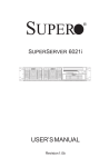
SUPER
SUPER
SUPER
SUPER
SUPER
P4SGA
P4SGL
P4SGR
P4SGE
USER’S MANUAL
Revision 1.1c
®
The information in this User’s Manual has been carefully reviewed and is believed to be
accurate. The vendor assumes no responsibility for any inaccuracies that may be contained
in this document, makes no commitment to update or to keep current the information in this
manual, or to notify any person or organization of the updates. Please Note: For the
most up-to-date version of this manual, please see our web site at
www.supermicro.com.
SUPERMICRO COMPUTER reserves the right to make changes to the product described in
this manual at any time and without notice. This product, including software, if any, and
documentation may not, in whole or in part, be copied, photocopied, reproduced, translated
or reduced to any medium or machine without prior written consent.
IN NO EVENT WILL SUPERMICRO COMPUTER BE LIABLE FOR DIRECT, INDIRECT,
SPECIAL, INCIDENTAL, OR CONSEQUENTIAL DAMAGES ARISING FROM THE USE OR
INABILITY TO USE THIS PRODUCT OR DOCUMENTATION, EVEN IF ADVISED OF THE
POSSIBILITY OF SUCH DAMAGES. IN PARTICULAR, THE VENDOR SHALL NOT HAVE
LIABILITY FOR ANY HARDWARE, SOFTWARE, OR DATA STORED OR USED WITH THE
PRODUCT, INCLUDING THE COSTS OF REPAIRING, REPLACING, INTEGRATING,
INSTALLING OR RECOVERING SUCH HARDWARE, SOFTWARE, OR DATA.
Any disputes arising between manufacturer and customer shall be governed by the laws of
Santa Clara County in the State of California, USA. The State of California, County of Santa
Clara shall be the exclusive venue for the resolution of any such disputes. Supermicro's total
liability for all claims will not exceed the price paid for the hardware product.
Unless you request and receive written permission from SUPER MICRO COMPUTER, you
may not copy any part of this document.
Information in this document is subject to change without notice. Other products and
companies referred to herein are trademarks or registered trademarks of their respective
companies or mark holders.
Copyright © 2003 by SUPER MICRO COMPUTER INC.
All rights reserved.
Printed in the United States of America
Preface
Preface
About This Manual
This manual is written for system integrators, PC technicians and
knowledgeable PC users. It provides information for the installation and use of
the SUPER P4SGA/P4SGL/P4SGR/P4SGE motherboard. The P4SGA/
P4SGL/P4SGR/P4SGE supports single Intel Pentium ® 4 1.5 - 3.06 GHz processors at a system bus speed of 533/400 MHz (3.0 GHz and 400 MHz only for
P4SGL).
Refer to the support section of our web site ( http://
www.supermicro.com/TechSupport.htm) for a listing of supported processors.
Single 478-pin Pentium 4 processors are housed in a 478-pin microPGA (Plastic Grid Array) package. This product is intended to be professionally installed.
Manual Organization
Chapter 1 includes a checklist of what should be included in your mainboard
box, describes the features, specifications and performance of the P4SGA/
P4SGL/P4SGR/P4SGE mainboard and provides detailed information about the
chipset.
Chapter 2 begins with instructions on handling static-sensitive devices. Read
this chapter when installing the processor and DDR memory modules and
when mounting the mainboard in the chassis. Also refer to this chapter to
connect the floppy and hard disk drives, the IDE interfaces, the parallel and
serial ports, the mouse and keyboard and the twisted wires for the power
supply, the reset button, the keylock/power LED and the speaker.
If you encounter any problems, see Chapter 3, which describes troubleshooting procedures for the video, the memory and the setup configuration stored in
CMOS. For quick reference, a general FAQ (Frequently Asked Questions)
section is provided. Instructions are also included for contacting technical
support. In addition, you can visit our web site at www.supermicro.com/
techsupport.htm for more detailed information.
Chapter 4 includes an introduction to BIOS and provides detailed information
on running the CMOS Setup utility.
Appendix A provides AwardBIOS POST Codes.
Appendix B lists AwardBIOS POST Messages.
Appendix C lists AwardBIOS Error Beep Codes.
iii
SUPER P4SGA/P4SGL/P4SGR/P4SGE User’s Manual
Table of Contents
Preface
About This Manual ...................................................................................................... iii
Manual Organization ................................................................................................... iii
Chapter 1: Introduction
1-1
Overview .......................................................................................................... 1-1
Checklist ..................................................................................................... 1-1
Contacting Supermicro ............................................................................. 1-2
SUPER P4SGA/P4SGL Image ............................................................... 1-4
SUPER P4SGR/P4SGE Image ............................................................... 1-5
SUPER P4SGA/P4SGL Layout .............................................................. 1-6
SUPER P4SGA/P4SGL Quick Reference .............................................. 1-7
SUPER P4SGR/P4SGE Layout .............................................................. 1-8
SUPER P4SGR/P4SGE Quick Reference ............................................. 1-9
845G Chipset: System Block Diagram ................................................. 1-10
Motherboard Features ........................................................................... 1-11
1-2
Chipset Overview .......................................................................................... 1-13
1-3
PC Health Monitoring ................................................................................... 1-14
1-4
Power Configuration Settings ...................................................................... 1-15
1-5
Power Supply ................................................................................................ 1-17
1-6
Super I/O ......................................................................................................... 1-18
Chapter 2: Installation
2-1
Static-Sensitive Devices ................................................................................ 2-1
2-2
Processor and Heatsink Installation ............................................................. 2-2
2-3
Mounting the Motherboard in the Chassis .................................................. 2-4
2-4
Installing DDR Memory .................................................................................. 2-5
2-5
I/O Port/Front Control Panel Connector Locations .................................... 2-6
2-6
Connecting Cables ......................................................................................... 2-8
Power Supply Connectors ....................................................................... 2-8
IR Connector .............................................................................................. 2-8
PW_ON Connector ................................................................................... 2-9
Reset Connector ........................................................................................ 2-9
IDE LED ..................................................................................................... 2-9
Power_LED Connector ........................................................................... 2-10
Keylock Connector ................................................................................. 2-10
Speaker Connector ................................................................................ 2-10
Serial Ports ............................................................................................. 2-10
iv
Table of Contents
CD Header .............................................................................................. 2-11
Fan Headers ........................................................................................... 2-11
Chassis Intrusion .................................................................................... 2-11
ATX PS/2 Keyboard/Mouse Ports ........................................................ 2-12
Universal Serial Bus (USB) .................................................................. 2-12
Wake-On-LAN .......................................................................................... 2-12
Wake-On-Ring ......................................................................................... 2-13
AC'97 Output ........................................................................................... 2-13
2-7
Jumper Settings ............................................................................................ 2-14
Explanation of Jumpers ......................................................................... 2-14
CMOS Clear ............................................................................................ 2-14
USB Wake-Up .......................................................................................... 2-15
Watch Dog Enable/Disable .................................................................... 2-15
Front Side Bus Speed ............................................................................ 2-15
Keyboard Wake-Up ................................................................................. 2-16
Speech Output Select ............................................................................. 2-16
LAN1 Enable/Disable .............................................................................. 2-17
LAN2 Enable/Disable .............................................................................. 2-18
SCSI Enable/Disable .............................................................................. 2-18
SCSI Channel A/B Termination Enable/Disable ................................. 2-18
Chassis/Overheat Fan Select ................................................................ 2-18
2-8
Game Port, Parallel Port, Floppy/Hard Drive and AGP Connections .... 2-19
Game Port Connector ............................................................................ 2-19
Parallel Port Connector ......................................................................... 2-19
Ultra160 SCSI Connectors ..................................................................... 2-20
Floppy Connector ................................................................................... 2-20
IDE Connectors ...................................................................................... 2-21
AGP Slot ................................................................................................... 2-21
2-9
Installing Software ........................................................................................ 2-22
SuperO Doctor II ..................................................................................... 2-23
Voice BIOS Editor ................................................................................... 2-24
Chapter 3: Troubleshooting
3-1
Troubleshooting Procedures ......................................................................... 3-1
Before Power On ...................................................................................... 3-1
No Power ................................................................................................... 3-1
No Video .................................................................................................... 3-1
Memory Errors .......................................................................................... 3-2
Losing the System’s Setup Configuration ............................................. 3-2
v
SUPER P4SGA/P4SGL/P4SGR/P4SGE User’s Manual
3-2
Technical Support Procedures ...................................................................... 3-2
3-3
Frequently Asked Questions ......................................................................... 3-3
3-4
Returning Merchandise for Service .............................................................. 3-6
Chapter 4: AwardBIOS
4-1
Introduction ....................................................................................................... 4-1
4-2
Running Setup .................................................................................................. 4-2
4-3
Main BIOS Setup ............................................................................................. 4-2
4-4
Advanced BIOS Setup .................................................................................... 4-6
Main BIOS Setup Menu ........................................................................... 4-3
4-4.1 Advanced BIOS Features ............................................................ 4-6
4-4.2 Advanced Chipset Features ........................................................ 4-9
4-4.3 Integrated Peripherals ................................................................ 4-13
4-4.4 Hardware Monitors ..................................................................... 4-16
4-4.5 Processor & Over-Clock ............................................................ 4-17
4-5
PCI/PnP Configurations ................................................................................ 4-18
4-6
Power .............................................................................................................. 4-20
4-7
Boot ................................................................................................................. 4-23
4-8
Security ........................................................................................................... 4-25
4-9
Exit ................................................................................................................... 4-26
Appendices:
Appendix A: AwardBIOS POST Messages ............................................................ A-1
Appendix B: AwardBIOS POST Codes ................................................................... B-1
Appendix C: AwardBIOS Error Beep Codes .......................................................... C-1
vi
Chapter 1: Introduction
Chapter 1
Introduction
1-1
Overview
Checklist
Congratulations on purchasing your computer motherboard from an acknowledged leader in the industry. Supermicro boards are designed with
the utmost attention to detail to provide you with the highest standards in
quality and performance.
Please check that the following items have all been included with your
motherboard. If anything listed here is damaged or missing, contact your
retailer.
All Included with Retail Box Only
One (1) Supermicro Mainboard
One (1) ATA66/100 ribbon cable for IDE devices
One (1) floppy drive ribbon cable
One (1) serial port (COM) cable
One (1) CPU retention bracket
One (1) USB 4-port cable (retail only)
One (1) I/O shield
One (1) Supermicro CD or diskettes containing drivers and utilities
One (1) User's/BIOS Manual
SCSI Accessories (P4SGR only)
One (1) 68-pin LVD SCSI cable
One (1) set of SCSI driver disketttes
One (1) SCSI manual
1-1
SUPER P4SGA/P4SGL/P4SGR/P4SGE User’s Manual
Contacting Supermicro
Headquarters
Address:
Tel:
Fax:
Email:
Web Site:
SuperMicro Computer, Inc.
980 Rock Ave.
San Jose, CA 95131 U.S.A.
+1 (408) 503-8000
+1 (408) 503-8008
[email protected] (General Information)
[email protected] (Technical Support)
www.supermicro.com
Europe
Address:
Tel:
Fax:
Email:
SuperMicro Computer B.V.
Het Sterrenbeeld 28, 5215 ML
's-Hertogenbosch, The Netherlands
+31 (0) 73-6400390
+31 (0) 73-6416525
[email protected] (General Information)
[email protected] (Technical Support)
[email protected] (Customer Support)
Asia-Pacific
Address:
SuperMicro, Taiwan
D5, 4F, No. 16 Chien-Ba Road
Chung-Ho 235, Taipei Hsien, Taiwan, R.O.C.
Tel:
+886-(2) 8226-3990
Fax:
+886-(2) 8226-3991
Web Site:
www.supermicro.com.tw
Technical Support:
Email:
[email protected]
Tel:
886-2-8226-3990, ext.132 or 139
1-2
Chapter 1: Introduction
Notes
1-3
SUPER P4SGA/P4SGL/P4SGR/P4SGE User’s Manual
SUPER P4SGA/P4SGL
Figure 1-1. SUPER P4SGA/P4SGL Image*
* The P4SGL has the same layout but no 4xAGP slot.
1-4
Chapter 1: Introduction
SUPER P4SGR/P4SGE
Figure 1-2. SUPER P4SGR/P4SGE Image*
* The P4SGE has the same layout but no onboard SCSI.
1-5
SUPER P4SGA/P4SGL/P4SGR/P4SGE User’s Manual
JPWAKE
JPUSB
CPU FAN
J24
J21
+12V Power Connector
ATX Power Connector
Keyboard/
Mouse
Motherboard (P4SGA//P4SGL) Layout*
(not drawn to scale)
J17
COM1
DIMM1
J15
J5
USB0/1
Ethernet Port
GMCH
CHASSIS FAN2
IDE #1
LINE
IN
IDE #2
LINE
OUT
GAME PORT
J7
J6
JP1
MIC
AGP 4x (1.5v)
J1
CHASSIS FAN1
PCI 1
LE2
BATTERY
PCI 2
PCI 3
P4SGA
PCI 4
CD1
®
CD2
ICH4
PCI 5
WOL
PCI 6
JA1
COM2
BIOS
USB4/5 USB2/3
JP3 JWOR1
JBT1
JL1 JOH1
JP2
SUPER
Center/subwoofer / Rear L&R / Rear L&R
VGA
DIMM2
Parallel Port
CPU
478 mPGA
FLOPPY
Figure 1-3.
JF1
JF2
*The P4SGL has the same layout but no 4xAGP slot.
*The P4SGA+ has the same layout - see page 1-11 for differences.
See Chapter 2 for detailed information on jumpers, I/O ports and JF1/JF2
Front Panel connections.
Jumpers not indicated are for test purposes only.
1-6
Chapter 1: Introduction
P4SGA/P4SGL Quick Reference
Jumpers
JBT1
JP1
JP2
JP3
JPUSB
JPWAKE
Description
CMOS Clear
Front Side Bus Speed
Watch Dog Enable
Speech Output Select
USB0/1 Wake Up
Keyboard Wake-Up
Default Setting
See Section 2-7
Pins 1-2 (Auto)
Open (Disabled)
Pins 1-2 (Speaker)
Pins 1-2 (Disabled)
Pins 1-2 (Disabled)
Connectors
CD1
CD2
Chassis Fan1/2
COM1/COM2
CPU Fan
DIMM1/2
Ethernet
Game Port
J1*
J5
J6/J7
J15
J17
J21
J24**
JA1
JF1, JF2
JL1
JOH 1
JWOR1
LE2
LINE IN
LINE OUT
MIC
USB2/USB3
USB4/USB5
WOL
Description
Audio CD Input (large connector)
Audio CD Input (small connector)
Chassis Fan Header
COM1/COM2 Serial Port Connector/Header
CPU Fan Header
Memory (DIMM) Slots
LAN (Ethernet Port)
Game Port
4xAGP
Floppy Disk Drive Connector
IDE #1/#2 Hard Disk Drive Connectors
Parallel Printer Port
PS/2 Keyboard/Mouse
ATX 12V Power Connector (20-pin)
ATX 12V Power Connector (4pin)
SPDIF Connector
Front Control Panel
Chassis Intrusion Header
Overheat LED
Wake-On-Ring Header
5v Standby Warning LED
Audio In Connector
Audio Out (Speaker) Connector
Microphone Input
Universal Serial Bus Port 2/3
Universal Serial Bus Port 4/5
Wake-On-LAN
* P4SGA only
** The 4-pin connector at J24 must be connected to meet the safety
requirements of the ATX 12V specifications.
1-7
SUPER P4SGA/P4SGL/P4SGR/P4SGE User’s Manual
Figure 1-4.
Keyboard/
Mouse
JPWAKE
JPUSB
J12
Motherboard (P4SGR/P4SGE) Layout*
(not drawn to scale)
J21
ATX Power Connector
+12V Power Connector
J17
J24
USB0/1
COM1
Parallel Port
COM2
JF1
CPU
478 mPGA
J15
CPU FAN
GMCH
JOH1
JP1
LAN1
DIMM1
LAN2
JP3
DIMM2
OVERHEAT FAN
VGA
Speaker
CHASSIS FAN1
AGP 4x (1.5v)
IDE #2
ICH4
PCI 4
SUPER
SCSI Channel B
JA2
JPA3
J7
J6
BATTERY
AIC7899
PCI 5
USB4/5
SCSI Channel B
WOL
SCSI Channel A
P4SGR
BIOS
JP2
PCI 3
®
JPL2
JPL1
PCI 2
IDE #1
LE2
PCI 1
USB2/3
JA3
JA1
JBT1 JPA2
JWOR1
CHASSIS FAN2
Speaker
JL1
JPA1
FLOPPY
J5
*The P4SGE has the same layout but no onboard SCSI.
See Chapter 2 for detailed information on jumpers, I/O ports and JF1 Front
Panel connections.
Jumpers not indicated are for test purposes only.
1-8
Chapter 1: Introduction
P4SGR/P4SGE Quick Reference
Jumpers
JBT1
JP1
JP2
JP3
JPA1*
JPA2*
JPA3*
JPL1/JPL2
JPUSB
JPWAKE
Description
CMOS Clear
Front Side Bus Speed
Watch Dog Enable
Fan Select
SCSI CH A Termination
SCSI CH B Termination
SCSI Enable/Disable
LAN1/LAN2 En/Dis
USB0/1 Wake Up
Keyboard Wake-Up
Default Setting
See Section 2-7
Pins 1-2 (Auto)
Open (Disabled)
Open (OH Fan)
Open (Enabled)
Open (Enabled)
Pins 1-2 (Enabled)
Pins 1-2 (Enabled)
Pins 1-2 (Disabled)
Pins 1-2 (Disabled)
Connectors
Chassis Fan1/2
COM1/COM2
CPU Fan
DIMM1/2
J1
J5
J6/J7
J12
J15
J17
J21
J24**
JA1/JA2/JA3*
JF1
JL1
JOH 1
JWOR1
LAN1/LAN2
LE2
Overheat Fan
USB0/1
USB2/3/4/5
WOL
Description
Chassis Fan Header
COM1/COM2 Serial Port Connector/Header
CPU Fan Header
Memory (DIMM) Slots
4xAGP
Floppy Disk Drive Connector
IDE #1/#2 Hard Disk Drive Connectors
Infrared Header
Parallel Printer Port
PS/2 Keyboard/Mouse
ATX 12V Power Connector (20-pin)
ATX 12V Power Connector (4pin)
Ultra160 SCSI Channel A/B/B
Front Control Panel
Chassis Intrusion Header
Overheat LED
Wake-On-Ring Header
Gb Ethernet Ports
5v Standby Warning LED
Overheat (Thermal) Fan
Universal Serial Bus Port 0/1
Universal Serial Bus Header 2/3/4/5
Wake-On-LAN
* P4SGR only
** The 4-pin connector at J24 must be connected to meet the safety
requirements of the ATX 12V specifications.
1-9
SUPER P4SGA/P4SGL/P4SGR/P4SGE User’s Manual
Pentium 4 Processor
(PGA 478)
DDR SDRAM
400/533 MHz System Bus
266 MHz Bus
4xAGP
GMCH
FC-PGA
1.06 GB/s
On chip
VGA
266 MB/s Hub
Flash BIOS
FWH
ICH4
Mb LAN
Port
Audio
CODEC
PCI Slots
133 MB/s PCI Bus
AC'97
Keyboard/Mouse
LPC Bus
USB
Ports (6)
Floppy Drive
USB 2.0
Dual Channel
IDE (PRI/SEC)
LPC I/O
Serial Ports
Parallel Port
UDMA/100
Game Port
Monitor
Figure 1-5. 845G* Chipset:
System Block Diagram
Note: This is a general block diagram and may not exactly
represent the features on your motherboard. See the following pages for the actual specifications of each motherboard.
*The 845GL (for the P4SGL) is the same but does not include support for
AGP and supports a 400 MHz System Bus only.
*The 845GE (for the P4SGR, P4SGE and P4SGA+) is the same but
supports PC2100 and PC2700 (DDR-266/DDR-333) only.
1-10
Chapter 1: Introduction
Motherboard Features
CPU
Latest CPU technology!
• Single Pentium ® 4 478-pin mPGA 1.5 - 3.06 GHz processors at a 533/
400 MHz system bus speed. P4SGL: 400 MHz system bus only.
(P4SGA+: same as P4SGA but also supports hyper-threading.)
Memory
Latest memory technology!
• Two 184-pin DIMM slots for up to 2 GB of non-ECC unbuffered
PC2100/1600 (DDR-266/200) SDRAM (PC2700/2100 for P4SGR/P4SGE/
P4SGA+)
Note: See Section 2-4 for details.
Chipset
Latest Intel chipset technology!
• Intel 845G Chipset - P4SGA
•
Intel 845GL Chipset - P4SGL
• Intel 845GE Chipset - P4SGR/P4SGE/P4SGA+
Expansion Slots
• Six 32-bit, 33 MHz PCI slots (P4SGA/P4SGL/P4SGA+)
• Five 32-bit, 33 MHz PCI slots (P4SGR/P4SGE)
• One 1.5V 4xAGP slot (P4SGA/P4SGR/P4SGE)
BIOS
With the latest voice BIOS technology for POST messaging!*
• 4 Mb Firmware Hub AwardBIOS ® Flash BIOS
• APM 1.2, DMI 2.3, PCI 2.2, ACPI 1.0, Plug and Play (PnP)
PC Health Monitoring
• Nine onboard voltage monitors for CPU core, chipset voltage, +3.3V,
+3.3V standby, +5V, +5V standby, Vbat (battery voltage) and ±12V
• Fan status monitor with firmware/software on/off control
• SuperDoctor II Utility
• Environmental temperature monitoring and control
• Power-up mode control for recovery from AC power loss
• System overheat LED and control
• System resource alert
• Hardware BIOS virus protection
• Auto-switching voltage regulator for the CPU core
*P4SGA/P4SGL/P4SGA+ only
1-11
SUPER P4SGA/P4SGL/P4SGR/P4SGE User’s Manual
ACPI Features
• Microsoft OnNow
• Slow blinking LED for suspend state indicator
• BIOS support for USB keyboard
• Real-time clock wake-up alarm
• Main switch override mechanism
• Internal/external modem ring-on
Onboard I/O
• Dual Ultra DMA 100 IDE Bus Masters
• Adaptec AIC-7899W for dual channel Ultra160 SCSI (P4SGR only)
• 1 floppy port interface (up to 2.88 MB)
• 2 Fast UART 16550A compatible serial ports
• 1 10/100 Mb LAN Ethernet port (works with integrated MAC - P4SGA/
P4SGL/P4SGA+)
• Intel 82540EM Gb Ethernet Controller for dual Gb ports (P4SGR/P4SGE)
• 1 EPP (Enhanced Parallel Port) and ECP (Extended Capabilities Port)
supported parallel port
•
PS/2 mouse and PS/2 keyboard ports
• Integrated high-perfomance "on-chip" Intel Extreme Graphics
• 1 game port with audio (P4SGA/P4SGL/P4SGA+)
channel sound technology!
• Up to 6 USB (Universal Serial Bus) ports
Latest onboard 6-
Latest USB 2.0 technology!
• 1 infrared port
Other
• Wake-on-LAN (WOL)
• Multiple CPU clock frequency ratio selections (set in BIOS)
• AC97' CODEC
• Suspend-to-RAM
• Onboard +5vsb warning LED ("LE2")
CD Utilities
• BIOS flash upgrade utility
• Drivers and software for 845GE/845G/845GL chipset utilities
Dimensions
• P4SGA/P4SGL/P4SGA+: ATX form factor, 12" x 8.7" (305 x 221 mm)
• P4SGR/P4SGE: ATX form factor, 12" x 9.5" (305 x 241 mm)
1-12
Chapter 1: Introduction
1-2
Chipset Overview
Intel’s 845G chipset (P4SGA) is made up of two primary components: the
Graphics Memory Controller Hub (GMCH) and the I/O Controller Hub (ICH4).
The 845GL (P4SGL) and 845GE (P4SGR/P4SGE) chipsets also include these
components, however the 845GL provides no AGP support and only a 400
MHz system bus speed and the 845GE supports faster memory.
Graphics Memory Controller Hub (GMCH)
The GMCH includes the host (CPU) interface, memory interface, ICH4 interface and 4xAGP interface for the 845G/GL/GE chipset. It contains advanced power management logic and supports a single channel of DDR
SDRAM. The AGP 2.0 interface supports 4x data transfers and operates at
a peak bandwidth of 1.6 GB/s.
An external graphics accelerator card is not required due to the integrated
graphics in the 845G/GL/GE chipset. (If the system BIOS detects an external AGP device, it will disable the integrated graphics.) The integrated
graphics controller delivers 3D, 2D and video capabilities, including video
conferencing applications. The controller does not utlilize local memory, but
accesses graphics data located in system memory at speeds matching that
of the SDRAM installed. It also includes a cache controller to avoid frequent
memory fetches of recently accessed texture data.
I/O Controller Hub (ICH4)
The ICH4 is a fourth-generation I/O Controller Hub subsystem that integrates
many of the input/output functions of the chipset, including a two-channel
ATA100 Bus Master IDE controller. The ICH4 also interfaces with the PCI
cards, the AC'97 Audio CODEC and the various communications ports.
Nearly all communications between the GMCH and the ICH4 takes place
over the hub Interface, which is a 66 MHz/266 MB/s bus.
Recovery from AC Power Loss
BIOS provides a setting for you to determine how the system will respond
when AC power is lost and then restored to the system. You can choose
for the system to remain powered off (in which case you must hit the
power switch to turn it back on) or for it to automatically return to a power
on state. See the Power Lost Control setting in the BIOS chapter of this
manual to change this setting. The default setting is Always OFF.
1-13
SUPER P4SGA/P4SGL/P4SGR/P4SGE User’s Manual
1-3
PC Health Monitoring
This section describes the PC health monitoring features of the SUPER
P4SGA/P4SGL/P4SGR/P4SGE. The motherboard has an onboard System
Hardware Monitor chip that supports PC health monitoring.
Nine Onboard Voltage Monitors for the CPU Core, Chipset
Voltage, +3.3V, +3.3V standby, + 5V, +5V standby, Vbat and
± 12V
The onboard voltage monitor will scan these voltages continuously. Once a
voltage becomes unstable, it will give a warning or send an error message
to the screen. Users can adjust the voltage thresholds to define the sensitivity of the voltage monitor.
Fan Status Monitor with Firmware/Software On/Off Control
The PC health monitor can check the RPM status of the cooling fans. The
onboard 3-pin fans are controlled by the power management functions.
Environmental Temperature Control
The P4SGA/P4SGL/P4SGR/P4SGE has a CPU "thermal trip" feature. A thermal control sensor monitors the CPU temperature in real time and will send
a signal to shut down the system whenever the CPU temperature exceeds
a certain threshold. This works to protect the CPU from being damaged by
overheating.
CPU Overheat LED and Control
This feature is available when the user enables the CPU overheat warning
function in the BIOS. This allows the user to define an overheat temperature. When this temperature is exceeded, the CPU thermal trip feature will
activate and shut down the system.
Hardware BIOS Virus Protection
The system BIOS is protected by hardware so that no virus can infect the
BIOS area. The user can only change the BIOS content through the flash
utility provided by Supermicro. This feature can prevent viruses from infecting the BIOS area and destroying valuable data.
1-14
Chapter 1: Introduction
Auto-Switching Voltage Regulator for the CPU Core
The 3-phase-switching voltage regulator for the CPU core can support up to
60A current and auto-sense voltage IDs ranging from 1.1V to 1.85V. This
will allow the regulator to run cooler and thus make the system more stable.
1-4
Power Configuration Settings
This section describes features of your motherboard that deal with power
and power settings.
Microsoft OnNow
The OnNow design initiative is a comprehensive, system-wide approach to
system and device power control. OnNow is a term for a PC that is always
on but appears to be off and responds immediately to user or other requests.
Slow Blinking LED for Suspend-State Indicator
When the CPU goes into a suspend state, the chassis power LED will start
blinking to indicate that the CPU is in suspend mode. When the user presses
any key, the CPU will wake-up and the LED will automatically stop blinking
and remain on.
BIOS Support for USB Keyboard
If the USB keyboard is the only keyboard in the system, it keyboard will
function like a normal keyboard during system boot-up.
Real Time Clock Wake-Up Alarm
Although the PC may be perceived to be off when not in use, it is still
capable of responding to preset wake-up events. In the BIOS, the user can
set a timer to wake-up the system at a predetermined time.
Main Switch Override Mechanism
When an ATX power supply is used, the power button can function as a
system suspend button. When the user depresses the power button, the
system will enter a SoftOff state. The monitor will be suspended and the
1-15
SUPER P4SGA/P4SGL/P4SGR/P4SGE User’s Manual
hard drive will spin down. Depressing the power button again will cause
the whole system to wake-up. During the SoftOff state, the ATX power
supply provides power to keep the required circuitry in the system alive. In
case the system malfunctions and you want to turn off the power, just
depress and hold the power button for 4 seconds. The power will turn off
and no power will be provided to the motherboard.
Wake-On-Ring Header
Wake-up events can be triggered by a device such as the external modem
ringing when the system is in the SoftOff state. Note that external modem
ring-on can only be used with an ATX 2.01 (or above) compliant power
supply.
Wake-On-LAN (WOL)
Wake-On-LAN is defined as the ability of a management application to remotely power up a computer that is powered off. Remote PC setup, updates and asset tracking can occur after hours and on weekends so that
daily LAN traffic is kept to a minimum and users are not interrupted. The
motherboards have a 3-pin header (WOL) to connect to the 3-pin header on
a Network Interface Card (NIC) that has WOL capability. Wake-On-LAN
must be enabled in BIOS. Note that Wake-On-Lan can only be used with an
ATX 2.01 (or above) compliant power supply.
1-16
Chapter 1: Introduction
1-5
Power Supply
As with all computer products, a stable power source is necessary for
proper and reliable operation. It is even more important for processors that
have high CPU clock rates of 1 GHz and faster.
The SUPER P4SGA/P4SGL/P4SGR/P4SGE accommodates 12V ATX power
supplies. Although most power supplies generally meet the specifications
required by the CPU, some are inadequate. You power supply must supply
1 amp of 5V standby voltage.
It is strongly recommended that you use a high quality power supply that
meets 12V ATX power supply Specification 1.1 or above. Additionally, in
areas where noisy power transmission is present, you may choose to install a line filter to shield the computer from noise. It is recommended that
you also install a power surge protector to help avoid problems caused by
power surges.
It also provides two high-speed, 16550 compatible serial communication
ports (UARTs), one of which supports serial infrared communication. Each
UART includes a 16-byte send/receive FIFO, a programmable baud rate
generator, complete modem control capability and a processor interrupt system. Both UARTs provide legacy speed with baud rate of up to 115.2 Kbps
as well as an advanced speed with baud rates of 250 K, 500 K, or 1 Mb/s,
which support higher speed modems.
The Super I/O provides functions that comply with ACPI (Advanced Configuration and Power Interface), which includes support of legacy and ACPI
power management through a SMI or SCI function pin. It also features auto
power management to reduce power consumption.
The IRQs, DMAs and I/O space resources of the Super I/O can be flexibly
adjusted to meet ISA PnP requirements, which suppport ACPI and APM (Advanced Power Management).
1-17
SUPER P4SGA/P4SGL/P4SGR/P4SGE User’s Manual
1-6
Super I/O
The disk drive adapter functions of the Super I/O chip include a floppy disk
drive controller that is compatible with industry standard 82077/765, a data
separator, write pre-compensation circuitry, decode logic, data rate selection, a clock generator, drive interface control logic and interrupt and DMA
logic. The wide range of functions integrated onto the Super I/O greatly
reduces the number of components required for interfacing with floppy disk
drives. The Super I/O supports four 360 K, 720 K, 1.2 M, 1.44 M or 2.88 M
disk drives and data transfer rates of 250 Kb/s, 500 Kb/s or 1 Mb/s.
1-18
Chapter 2: Installation
Chapter 2
Installation
2-1
Static-Sensitive Devices
Electric Static Discharge (ESD) can damage electronic components. To
prevent damage to your system board, it is important to handle it very
carefully. The following measures are generally sufficient to protect your
equipment from ESD.
Precautions
• Use a grounded wrist strap designed to prevent static discharge.
• Touch a grounded metal object before removing the board from the antistatic bag.
• Handle the board by its edges only; do not touch its components, peripheral chips, memory modules or gold contacts.
• When handling chips or modules, avoid touching their pins.
• Put the motherboard and peripherals back into their antistatic bags when
not in use.
• For grounding purposes, make sure your computer chassis provides excellent conductivity between the power supply, the case, the mounting
fasteners and the motherboard.
Unpacking
The motherboard is shipped in antistatic packaging to avoid static damage.
When unpacking the board, make sure the person handling it is static protected.
Installation Procedures
Follow the procedures as listed below for full installation of the motherboard
into a chassis:
1. Install the processor and the heatsink to the motherboard.
2. Install the motherboard in the chassis.
3. Install the memory and add-on cards.
4. Finally, connect the cables and install the drivers.
2-1
SUPER P4SGA/P4SGL/P4SGR/P4SGE User's Manual
2-2
Processor and Heatsink Fan Installation
!
When handling the processor package, avoid placing
direct pressure on the label area of the fan.
IMPORTANT: Always connect the power cord last and always remove it
before adding, removing or changing any hardware components. Make
sure that you install the processor into the CPU socket before you install the
CPU heatsink.
Installation of the Processor and Heatsink
1. Locate the following components, which are included in the shipping
package.
Clips (2)
Bracket (1)
Note: The CPU heatsink fan with clips is included only with the retail versions of the P4SGA/P4SGL/P4SGR/P4SGE. If you buy a boxed Intel Pentium
4 478/Northwood processor, it should include a heatsink, fan and retention
mechanism. If you buy a processor separately, use only a Supermicro or
Intel certified heatsink and fan.
2. Insert the white pegs into the black anchors. Do not force the white pegs all the
way in - about 1/3 of the white pegs should
be inside the black anchors. (These are for
chassis that do not have four CPU retention
holes.)
Bracket in
position
3. Place a retention bracket in the proper position
and secure it by pressing two pegs into the retention holes until you hear a *click*. The clicking
sound indicates that the peg is locked and secured.
4. Secure the other retention bracket into position by repeating Step 3.
2-2
Chapter 2: Installation
5. Lift the lever on the CPU socket.
Socket Lever
6. Install the CPU in the socket. Make sure that
Pin 1 of the CPU is seated on Pin 1 of the socket
(both corners are marked with a triangle).
7. Press the lever down until
you hear it *click* into the
locked position.
Socket lever in
locked position
8. Apply the proper amount of thermal compound to the CPU die.
9. Place the heatsink on top of
the CPU and press firmly downward - do not twist or slide
the heatsink to seat thermal
compound.
10. Secure the heat sink by
locking the retention clips into
their proper position.
Retainer clip
attachment
point
11. Connect the CPU fan cable to
the CPU Fan header on the
motherboard.
2-3
SUPER P4SGA/P4SGL/P4SGR/P4SGE User's Manual
Lever
Pin 1
Processor
(installed)
Pin 1
Figure 2-1. 478-pin mPGA Socket: Empty and with Processor Installed
2-3
Mounting the Motherboard in the Chassis
All motherboards have standard mounting holes to fit different types of
chassis. Make sure the location of all the mounting holes for both the
motherboard and the chassis match. Although a chassis may have both
plastic and metal mounting fasteners, metal ones are highly recommended
because they ground the motherboard to the chassis. Make sure the metal
standoffs click in or are screwed in tightly. Then use a screwdriver to
secure the motherboard onto the motherboard tray.
2-4
Chapter 2: Installation
2-4
Installing DDR Memory
CAUTION
Exercise extreme care when installing or removing memory
modules to prevent any possible damage.
Memory Module Installation (See Figure 2-2)
1.
Insert each DDR memory module vertically into its slot. Pay attention to
the notch along the bottom of the module to prevent inserting the module incorrectly. (See support information below.)
2.
Gently press down on the memory module until it snaps into place.
3.
Two 184-pin memory sockets support up to 2 GB unbuffered non-ECC
DDR type SDRAM (see support information below).
Support
The P4SGA/P4SGL supports both double-sided and single-sided nonregistered, unbuffered PC2100 (DDR-266) or PC1600 (DDR-200)
SDRAM. The P4SGR/P4SGE/P4SGA+ supports both double-sided and
single-sided non-registered, unbuffered PC2700 (DDR-333) or PC2100
(DDR-266) SDRAM. Always populate DIMM1 first.
Figure 2-2.
Side and Top Views of DDR Module Installation into Slot
To Install:
Insert module
vertically and
press down
until it snaps
into place.
Pay attention
to the notch.
To Remove:
Use your thumbs
gently to push
each release tab
outward to
release the DIMM
from the slot.
2-5
SUPER P4SGA/P4SGL/P4SGR/P4SGE User's Manual
2-5
I/O Port/Control Panel Connector Locations
The I/O ports are color coded in conformance with the PC99 specification to
make setting up your system easier. See Figure 2-3 below for the colors
and locations of the various IO ports.
Figure 2-3.
I/O Port Locations and Definitions
P4SGA/P4SGL
Mouse (Green)
Parallel Port (Burgundy)
Game Port (Gold)
LAN Port
Keyboard
COM1 Port (Turquoise)
VGA Port (Blue) USB 0/1 Ports
Line Out / Line In / Mic
(Lime) / (Light Blue) / (Pink)
(Purple)
P4SGR/P4SGE
Mouse (Green)
Keyboard
Parallel Port (Burgundy)
USB 0/1 Ports COM1 Port (Turquoise)
(Purple)
2-6
VGA Port (Blue)
LAN1
LAN2
Chapter 2: Installation
Front Control Panel
JF1/JF2 (P4SGA/P4SGL) and JF1 (P4SGR/P4SGE) contain header pins for
various front control panel connectors. See Figure 2-4 for the pin definitions of the various connectors included speaker. Refer to Section 2-6 for
details.
Figure 2-4.
Front Control Panel Connectors
P4SGA/P4SGL
R eset
Speaker
X
P ower O n
Keylock
X
X
Power_LED
X
IR C onnector
ID E LE D
1
JF1 JF2
1
P4SGR/P4SGE
20
19
NMI
Ground
X
X
Power LED
Vcc
HDD LED
Vcc
NIC1 LED
Vcc
NIC2 LED
Vcc
Overheat LED
Vcc
Power Fail LED
Vcc
Ground
Ground
2
JF1
2-7
1
Reset
Reset Button
Pwr
Power Button
SUPER P4SGA/P4SGL/P4SGR/P4SGE User's Manual
2-6
Connecting Cables
Power Supply Connectors
AT X 20-pin Po wer Connector
Pin Definitions (J21)
The primary power supply connector on the P4SGA/P4SGL/P4SGR/
P4SGE meets the SSI (Superset
ATX) 20-pin specification. Refer
to the table on the right for the pin
definitions of the ATX 20-pin
power connector. You must also
connect the 4-pin J24 power connector to your power supply. Refer to the table below right for the
J24 (12V) connector.
Pin #
11
12
13
14
15
16
17
18
19
20
Definition
+3.3V
-12V
COM
PS_ON
COM
COM
COM
-5V
+5V
+5V
Pin #
1
2
3
4
5
6
7
8
9
10
Definition
+3.3V
+3.3V
CO M
+5V
COM
+5V
CO M
PW -OK
5VSB
+12V
+12V 4-pin PW R
Connector
(J24)
Pins # Definition
1 &2
Ground
3 &4
+12 V
Required
Connection
PW R Supply
Color Definition
Color
Definition
Orange
+3.3V
Black
Com
Red
5V
W hite
Power OK
Yellow
+12V
Purple
5V standby
Brown
-5V
(For reference only)
IR Connector
The infrared connector is located
on pins 1-5 of JF1 on the P4SGA/
P4SGL and on J12 on the P4SGR/
P4SGE. See the tables on the right
for pin definitions. Refer to the
Technical Support section of our
web page for information on the
infrared devices you can connect
to the system.
2-8
Infrared
Pin Definitions
(JF1)
Infrared
Pin Definitions
(J12)
Pin
Number Definition
+5V
1
CIR
2
IRR X
3
Ground
4
IRT X
5
Pin
Number Definition
+5V
1
CIR
2
IRRX
3
Ground
4
IRTX
5
NC
6
Chapter 2: Installation
PW_ON Connector
The PW_ON connector is located
on pins 9 and 10 of JF1 on the
P4SGA/P4SGL (1 and 2 on the
P4SGR/P4SGE). This header
should be connected to the chassis power button, which you may
also configure to put the system
into suspend mode (see the Power
Button Mode setting in BIOS). To
turn off the power when the suspend mode is enabled, depress
the power button for at least 4
seconds. See the table on the
right for pin definitions.
Reset Connector
PW _ON
Pin Definitions
(JF1)
Pin
Number Definition
9
PW _O N
10
Ground
Reset Pin
Definitions
(JF 1)
The reset connector is located on
pins 12 and 13 of JF1 on the
P4SGA/P4SGL (3 and 4 on the
P4SGR/P4SGE). This connector
attaches to the reset switch on
the computer chassis. See the
table on the right for pin definitions.
IDE LED
Pin
Number Definition
Ground
12
Reset
13
IDE LED
Pin Definitions
(JF 2)
The IDE LED is located on pins 1 to
4 of JF2 on the P4SGA/P4SGL (13
and 14 of JF1 on the P4SGR/
P4SGE). This connects to the
hard drive LED to display hard
drive activity. See the table on the
right for pin definitions.
2-9
Pin
Number Definition
+5V
1
HD Active
2
HD Active
3
+5V
4
SUPER P4SGA/P4SGL/P4SGR/P4SGE User's Manual
Power_LED Connector
Power_LED
Pin Definitions (JF2)
The Power LED connector is located on pins 5-7 of JF2 on the
P4SGA/P4SGL (15 and 16 of JF1
on the P4SGR/P4SGE). This connection is used to provide LED indication of power being supplied
to the system. See the table on
the right for pin definitions.
Pin
Number
5
6
7
Keylock Connector
Definition
+5V
Key
Control
Keylock
Pin Definitions
(JF2)
The keylock connector is located
on pins 8 and 9 of JF2 on the
P4SGA/P4SGL. See the table on
the right for pin definitions.
Pin
Number Definition
8
+5V
9
Control
Speaker Connector
Speaker Pin
Definitions (JF2)
The speaker connector is located
on pins 10 to 13 of JF2 on the
P4SGA/P4SGL. See the table on
the right for pin definitions.
Pin
Definition
Number Function
+
R ed wire, Speaker data
10
Key
No connection
11
12
Key
No connection
Speaker data
13
Serial Ports
Serial Port Pin Definitions
(COM1, COM2)
Two serial ports are included on
the motherboard: COM1 is a port
located beside the mouse/keyboard ports and COM2 is a header
located on the motherboard near
PCI slot 6. See the table on the
right for pin definitions.
*NC indicates no connection.
2-10
Pin Number
1
2
3
4
5
Definition
CD
RD
TD
DTR
Ground
Pin Number
6
7
8
9
10
Definition
DSR
RTS
CTS
RI
NC
Note: Pin 10 is included on the header but not on
the port.
Chapter 2: Installation
CD Header (P4SGA/SGL)
There are two 4-pin CD headers
of
different
sizes
on
the
motherboard. These allow you to
use the onboard sound for audio
CD playback. Connect the audio
cable from your CD drive to the
header that fits your cable's connector. Only one CD header can
be use at any one time. See the
tables on the right for pin definitions.
Audio CD Header Pin Definitions
(CD1)
Pin
Number
Definition
1
2
3
4
Left Stereo Signal
Ground
Ground
Right Stereo Signal
Audio CD Header Pin Definitions
(CD2)
Pin
Number
1
2
3
4
Definition
Right Stereo Signal
Ground
Left Stereo Signal
Ground
Fan Headers
There are three fan headers on
the P4SGA/P4SGL, which are
designated CPU Fan, Chassis Fan
1 and Chassis Fan 2. The P4SGR/
P4SGE also has an Overheat Fan.
Connect the fan on your CPU
heatsink to the CPU Fan header.
See the table on the right for pin
definitions.
Fan Header Pin Definitions
(C PU, Chassis and Overheat)
Pin
Number
Definition
1
2
3
Ground (black)
+12V (red)
Tachometer
Caution: These fan headers are DC power.
Chassis Intrusion
The Chassis Intrusion header is
designated JL1. See the board
layout in Chapter 1 for the location
of JL1 and the table on the right
for pin definitions.
Chassis Intrusion
Pin Definitions (JL1)
Pin
Number
Definition
1
Intrusion Input
2
Ground
Overheat LED (JOH1)
Connect an LED to the JOH1
header to provide warning of
chassis overheating. See the
table on the right for pin definitions.
2-11
Overheat LED
Pin Definitions (JOH1)
Pin
Number
1
2
Definition
+5V
OH Active
SUPER P4SGA/P4SGL/P4SGR/P4SGE User's Manual
ATX PS/2 Keyboard and
PS/2 Mouse Ports
PS/2 Keyboard
and Mouse Port
Pin Definitions
(J17)
The ATX PS/2 keyboard and the
PS/2 mouse are located on J17.
See the table on the right for pin
definitions. (The mouse port is
above the keyboard port. See the
table on the right for pin definitions.
Universal Serial Bus (USB)
Two Universal Serial Bus 2.0 connectors (USB0 and USB1) are provided for backpanel access. See
the table on the right (above) for
pin definitions.
The P4SGA/
P4SGL/P4SGR/P4SGE also provides four additional USB 2.0
headers on the motherboard,
which may be used to provide
front side chassis access (cables
not included). These additional
ports are labeled USB2, USB3,
USB4 and USB5. See the tables
on the right (below) for pin definitions.
Pin
Number Definition
Data
1
NC
2
Ground
3
VCC
4
Clock
5
NC
6
USB0/USB1 Port Pin Definitions
(J18/J19)
Pin# Definition
1
+5V
2
P03
P0+
4 Ground
USB2/4
Pin
Number
1
2
3
4
5
Definition
+5V
POPO+
Ground
Key
USB3/5
Pin
Number
1
2
3
4
5
Definition
+5V
POPO+
Ground
Ground
Wake-On-LAN
The Wake-On-LAN header is designated WOL on the motherboard.
See the table on the right for pin
definitions. You must enable the
LAN Wake-Up setting in BIOS to
use this function. (You must also
have a LAN card with a Wake-OnLAN connector and cable to use
this feature.)
2-12
W ake-On-LAN Pin
Definitions (W OL)
Pin
Number
1
2
3
Definition
+5V Standby
Ground
W ake-up
Chapter 2: Installation
Wake-On-Ring
W ake-On-Ring Pin Definitions
(JW OR1)
The Wake-On-Ring header is designated JWOR. This function allows
your computer to receive and be
"awakened" by an incoming call when
in the suspend state. See the table on
the right for pin definitions. You must
also have a WOR card and cable to
use WOR.
Pin
Number
Definition
1
Ground
2
W ake-up
AC'97 Output (P4SGA/P4SGL)
AC'97 provides high quality onboard
audio. The P4SGA/P4SGL features 6channel sound for front L&R, rear
L&R, center and subwoofer speakers. This feature is activated with
the Avanc software (on the CDROM
included with your motherboard).
Sound is then output through the Line
In, Line Out and MIC jacks (see at
right). Activate AC 97 with the "AC
97 Audio" setting in the Advanced
Chipset Features section of BIOS.
2-13
Front L&R / Rear L&R / Center & Subwoofer
SUPER P4SGA/P4SGL/P4SGR/P4SGE User's Manual
2-7
Jumper Settings
Explanation of
Jumpers
To modify the operation of the
motherboard, jumpers can be used
to choose between optional settings. Jumpers create shorts between two pins to change the
function of the connector. Pin 1 is
identified with a square solder pad
on the printed circuit board. See
the motherboard layout pages for
jumper locations.
Connector
Pins
3
2
1
3
2
1
Jumper
Cap
Setting
Pin 1-2 short
No te : On a two-pin jumper,
"Closed" means the jumper is on
both pins and "Open" means the
jumper is either on only one pin or
completely removed.
CMOS Clear
JBT1 is used to clear CMOS. Instead
of pins, this jumper consists of contact pads to prevent accidentally
clearing the contents of CMOS.
To clear CMOS,
1) First unplug the power cord(s) .
2) With the power disconnected, short
the CMOS pads with a metal object
such as a small screwdriver.
3) Remove the screwdriver (or shorting device).
4) Reconnect the power cord(s) and
power on the system.
Note: Do not use the PW_ON connector to clear CMOS.
2-14
Chapter 2: Installation
USB Wake-Up
USB Wake-Up
Jumper Settings
(JPUSB)
Use JPUSB to enable or disable
USB Wake-Up, which allows you
to wakeup the system by depressing a key on the keyboard or
by clicking the mouse when either
is connected to the USB0 or USB1
port. This jumper is used together
with the USB Wake-Up function in
BIOS. Enable both the jumper and
the BIOS setting to allow the system to be woken up. See the table
on the right for jumper settings.
Jumper
Position
1-2
2-3
Definition
Disabled
Enabled
Watch Dog Enable/Disable
JP2 enables and disables the
Watch Dog function. Watch Dog
is a system monitor that will restart the system if a software application freezes operations. This
jumper is used together with the
Watch Dog enable function in
BIOS. Enable both the jumper and
the BIOS setting to use the Watch
Dog feature. See the table on the
right for jumper settings.
Front Side Bus Speed
W atch Dog Enable
Jumper Settings (JP2)
Jumper
Position
Open
Closed
Definition
Disabled
Enabled
Front Side Bus Speed
Jumper Settings (JP1)
JP1 is used to set the system
(front side) bus speed for the processors. It is best to keep this
jumper set to Auto. Note that the
P4SGL only supports 400 MHz
FSB speed. This jumper is used
together with the CPU Clock setting in BIOS. See the table on the
right for jumper settings.
2-15
Jum per
Position
Pins 1-2
Pins 2-3
Open
Definition
Auto
400 M Hz
533 M hz
SUPER P4SGA/P4SGL/P4SGR/P4SGE User's Manual
Keyboard Wake-Up
The JPWAKE jumper is used together with the Keyboard WakeUp function in BIOS. Enable both
the jumper and the BIOS setting to
allow the system to be woken up
by depressing a key on the keyboard. See the table on the right
for jumper settings. Your power
supply must meet ATX specification 2.01 or higher and supply 720
mA of standby power to use this
feature.
Speech Output Select
(P4SGA/P4SGL)
Keyboard W ake-Up
Jumper Settings
(JPW AKE)
Jumper
Position
1-2
2-3
Definition
Disabled
Enabled
Speech Output Select
Jumper Settings (JP3)
The system BIOS has a voice feature that it can use to inform you
of the POST (Power-On-Self-Test)
routine details. You can also program your voice to give the BIOS
certain commands with the software included on the Supermicro
CD that was included with your
motherboard. JP3 is used to direct
the BIOS voice output to either the
Line Out port or via the Speaker
header on JP2. The "Voice Warning Output" setting (in the Advanced BIOS Features section of
BIOS) must be enabled to use this
feature. See the table on the right
for jumper setting pin definitions.
2-16
Jumper
Position
1-2
2-3
Definition
Speaker
Line Out
Chapter 2: Installation
LAN1 Enable/Disable
(P4SGR/P4SGE)
Change the setting of jumper JPL1
to enable or disable the onboard
LAN1 or NIC (Network Interface
Card) on the motherboard. See
the table on the right for jumper
settings. The default setting is
Enabled.
LAN2 Enable/Disable
(P4SGR/P4SGE)
Change the setting of jumper JPL2
to enable or disable the onboard
LAN2 or NIC (Network Interface
Card) on the motherboard. See
the table on the right for jumper
settings. The default setting is
Enabled.
SCSI Enable/Disable
(P4SGR)
LAN1 (NIC)
Enable/Disable
Jumper Settings
(JPL1)
Jumper
Position
Pins 1-2
Pins 2-3
Definition
Enabled
Disabled
LAN2 (NIC)
Enable/Disable
Jumper Settings
(JPL2)
Jumper
Position
Pins 1-2
Pins 2-3
Definition
Enabled
Disabled
SCSI Enable/Disable
Jumper Settings
(JPA3)
The SCSI Termination jumper at
JPA3 allows you to enable or disable the onboard SCSI controller.
The normal (default) position is on
to enable SCSI termination. See
the table on the right for jumper
settings.
2-17
Jumper
Position
Pins 1-2
Pins 2-3
Definition
Enabled
Disabled
SUPER P4SGA/P4SGL/P4SGR/P4SGE User's Manual
SCSI Channel A/B
Termination Enable/Disable
(P4SGR)
Jumpers JPA1 and JPA2 allow you
to enable or disable termination for
the individual SCSI channels.
Jumper JPA1 controls SCSI channel
A and JPA2 controls SCSI channel
B. The normal (default) setting is
open to enable (teminate) both SCSI
channels. If you wish to connect
external SCSI devices, you should
disable
termination
for
the
channnel(s) you will be connecting
them to. See the table on the right
for jumper settings.
Chassis/Overheat Fan
Select (P4SGR/P4SGE)
SCSI Channel T ermination
Enable/Disable
Jumper Settings
(JPA1, JPA2)
Jumper
Position
Open
Closed
Definition
Enabled
Disabled
Chassis/Overheat Fan
Select Jumper Settings
(JP3)
JP3 allows you to select between
use of the Chassis fan and the
Overheat fan. The default position
is open to select the Overheat fan.
The CPU Chassis fan is intended for
use with Supermicro chassis. A
closed jumper setting forces the
chassis fan to always be on. See
the table on the right for jumper settings.
2-18
Jumper
Position
Closed
Open
Definition
Chassis Fan
Overheat Fan
Chapter 2: Installation
2-8
Game Port, Parallel Port, Floppy Drive, Hard Drive
and AGP Connections
Use the following information to connect the floppy and hard disk drive
cables.
• The floppy disk drive cable has seven twisted wires.
• A red mark on a wire typically designates the location of pin 1.
• A single floppy disk drive ribbon cable has 34 wires and two connectors to
provide for two floppy disk drives. The connector with twisted wires always
connects to drive A, and the connector that does not have twisted wires
always connects to drive B.
• The 80-wire ATA100/66 IDE hard disk drive cable that came with your
system has two connectors to support two drives. This special cable
should be used to take advantage of the speed this new technology
offers. The blue connector connects to the onboard IDE connector interface and the other connector(s) to your hard drive(s). Consult the documentation that came with your disk drive for details on actual jumper
locations and settings for the hard disk drive.
Game Port Pin Definitions
(GAME PORT )
Game Port Connector
(P4SGA/P4SGL)
The game port is the gold port on
the I/O backplane. See the table
on the right for pin definitions.
Pin Number Function Pin Number Function
1
+5V fused
2 GP4 (JSBUTO)
3
GP0 (JSX1R)
4
Ground
5
Ground
6
GP1 (JSY1R)
7
GP5 (JSBUT1)
8
+5V fused
9
+5V fused
10
GP6 (JSBUT2)
11
GP2 (JSX2R)
12
MIDI-OUTR
13
GP3 (JSY2R)
14
GP7 (JSBUT3)
15
MIDI-INR
Parallel (Printer) Port Pin Definitio ns
(J15)
Parallel Port Connector
The parallel port is located on J15.
See the table on the right for pin
definitions.
2-19
Pin Number
1
3
5
7
9
11
13
15
17
19
21
23
25
Function Pin Number Function
Strobe2
Auto FeedData Bit 0
4
ErrorData Bit 1
6
InitData Bit 2
8
SLCT INData Bit 3
10
GND
Data Bit 4
12
GND
Data Bit 5
14
GND
Data Bit 6
16
GND
Data Bit 7
18
GND
ACK
20
GND
BUSY
22
GND
PE
24
GND
SLCT
26
NC
SUPER P4SGA/P4SGL/P4SGR/P4SGE User's Manual
68-pin Ultra160 SCSI Connectors (JA1, JA2, JA3)
Ultra160 SCSI
Connectors
(P4SGR)
Refer to the table on
the right for the pin definitions of the Ultra160
SCSI connectors located at JA1, JA2 and
JA3.
Connector
Contact
Number
Signal Names
Connector
Contact
Number
Signal N ames
1
2
3
4
5
6
7
8
9
10
11
12
13
14
15
16
17
18
19
20
21
22
23
24
25
26
27
28
29
30
31
32
33
34
+DB(12)
+DB(13)
+DB(14)
+DB(15)
+DB(P1)
+DB(0)
+DB(1)
+DB(2)
+DB(3)
+DB(4)
+DB(5)
+DB(6)
+DB(7)
+DB(P)
GROUN D
DIFFSENS
TERMPW R
TERMPW R
RESERVED
GROUN D
+ATN
GROUN D
+BSY
+ACK
+RST
+MSG
+SEL
+C/D
+REQ
+I/O
+DB(8)
+DB(9)
+DB(10)
+DB(11)
35
36
37
38
39
40
41
42
43
44
45
46
47
48
49
50
51
52
53
54
55
56
57
58
59
60
61
62
63
64
65
66
67
68
-DB(12)
-DB(13)
-DB(14)
-DB(15)
-DB(P1)
-DB(0)
-DB(1)
-DB(2)
-DB(3)
-DB(4)
-DB(5)
-DB(6)
-DB(7)
-DB(P)
GROU ND
GROU ND
TERMPW R
TERMPW R
RESER VED
GROU ND
-ATN
GROU ND
-BSY
-ACK
-RST
-MSG
-SEL
-C/D
-REQ
-I/O
-DB(8)
-DB(9)
-DB(10)
-DB(11)
F loppy Connector Pin Definitions (JP5)
Floppy Connector
The floppy connector is located
on JP5. See the table on the right
for pin definitions.
Pin Number
1
3
5
7
9
11
13
15
17
19
21
23
25
27
29
31
33
2-20
Function
GND
GND
Key
GND
GND
GND
GND
GND
GND
GND
GND
GND
GND
GND
GND
GND
GND
Pin Number
Function
2
FD HDIN
4
Reserved
6
FD EDIN
8
Index10
Motor Enable
12
Drive Select B14
Drive Select A16
Motor Enable
18
DIR20
STEP22
W rite Data24
W rite Gate26
Track 0028
W rite Protect30
Read Data32
Side 1 Select34
Diskette
Chapter 2: Installation
IDE Connector Pin Definitions
(J6, J7)
Pin Number
1
3
5
7
9
11
13
15
17
19
21
23
25
27
29
31
33
35
37
39
Function
Reset IDE
Host Data 7
Host Data 6
Host Data 5
Host Data 4
Host Data 3
Host Data 2
Host Data 1
Host Data 0
GND
DRQ3
I/O W riteI/O ReadIOCHRDY
DACK3IRQ14
Addr 1
Addr 0
Chip Select 0
Activity
Pin Number
2
4
6
8
10
12
14
16
18
20
22
24
26
28
30
32
34
36
38
40
Function
G ND
Host Data 8
Host Data 9
Host Data 10
Host Data 11
Host Data 12
Host Data 13
Host Data 14
Host Data 15
Key
G ND
G ND
G ND
BALE
G ND
IOC S16G ND
Addr 2
Chip Select 1G ND
IDE Connectors
There are no jumpers to configure the onboard IDE interfaces
J6 and J7. See the table on the
left for pin definitions. You
must use the ATA100/66 cable
included with your system to
benefit from the ATA100/66
technology.
1.5V 4xAGP Slot (P4SGA/P4SGR/P4SGE)
The 4xAGP slot is not included on the P4SGL. You should first disable
the integrated video in BIOS before adding a VGA card to this slot. (See
the "On-Chip VGA" setting in the Advanced Chipset Features section in
BIOS.) The 4xAGP slot is backward compatible with 2xAGP graphics
cards.
To install a VGA card, power down the system and remove the I/O shield
corresponding to the AGP slot. Then, pull back the locking tab on the slot
before inserting your VGA card. After the card is inserted, close the
locking tab if possible (some VGA cards have a notch in the corner of
the board to lock it into place, others do not.) Replace all chassis covers
before restoring power to the system.
Locking Tab
2-21
SUPER P4SGA/P4SGL/P4SGR/P4SGE User's Manual
2-9
Installing Software
After all the hardware has been installed, you must install, first of all, the
operating system, and then, the software drivers. The necessary drivers
are all included on the Supermicro CD that came packaged with your
motherboard. After inserting this CD into your CDROM drive, the display
shown in Figure 2-5 should appear. (If this display does not appear, click
on the My Computer icon and then on the icon representing your CDROM
drive. Finally, double click on the S "Setup" icon.)
Figure 2-5. Driver/Tool Installation Display Screen
Click the icons showing a hand writing on paper to view the readme files
for each item. Click the computer icons to the right of these in order from
top to bottom to install each item one at a time. After installing each
item, you must reboot the system before moving on to the next
item on the list. You should install everything here except for the SUPER
Doctor utility and the LAN/SCSI driver diskettes, which are optional. The
Security and Graphics Drivers support multiple languages. Click the arrows
to pull down a menu of choices. The bottom icon with a CD on it allows you
to view the entire contents of the CD. Note: The memory size reported in
the device manager may be less than expected because some is used by
the onboard graphics. Higher screen resolutions will take up more of this
memory.
2-22